Embed Size (px)
Citation preview

8/8/2019 gate dri
http://slidepdf.com/reader/full/gate-dri 1/10
Hybrid Circuits Simplify IGBT Module Gate Drive
Eric R. MottoPowerex Inc., Youngwood, Pennsylvania, USA
Abstract: This paper will review the typical gate drive requirements for the latest generation of high power
IGBT modules and present simplified implementations of the required circuits using newly developedhybrid integrated circuit (HIC) building blocks. A newly developed circuit that provides short circuit
protection without desaturation detection will also be presented.
I. INTRODUCTION
In high power IGBT module applications it is usually desirable to use completely isolated gate
drive circuits. A typical implementation of this type of gate drive is shown in figure 1. This circuit provides
isolation of logic level control and fault feedback signals using optocouplers and separate isolated powersupplies for each gate driver. There are a number of advantages to this topology including: (1) Stable on
and off drive driving voltages that are independent of the power device switching duty. (2) Capable ofproviding very high output currents for large IGBT modules. (3) Power circuit switching noise and highvoltages are isolated from control circuits. (4)
Local power is available for protection circuitssuch as desaturation detectiont. The maindisadvantages of this type of driver are the
cost, complexity and board space requiredfor all of the isolated power supplies. Inaddition, these circuits can be difficult to
develop due to the severe requirements fornoise immunity and high isolation voltage. To
simplify the design of isolated gate drivePowerex/Mitsubishi has developed severalnew hybrid integrated circuits that supplygate drive, short circuit protection and
isolated gate drive power. This paper willdescribe the characteristics and operation ofthese newly developed hybrid circuits.
II. GENERAL GATE DRIVE REQUIREMENTS FOR HIGH POWER IGBT MODULES
The main components of a typical gate drive circuit are illustrated in the simplified circuit schematicshown in figure 2. The primary function of the gate drive circuit is to convert logic level control signals into the
appropriate voltage and current for efficient, reliable, switching of the IGBT module. An output driver stageconsisting of small power MOSFETs or bipolar transistors performsthe conversion by alternately connecting the IGBT’s gate to the
appropriate on (VON) and off (VOFF) voltages. The driver stagedevices and series gate resistance RG must be selected to providethe appropriate peak current for charging and discharging the
IGBT’s gate. Most gate drive circuits also provide isolation so thatthe logic signals are not connected to the dangerous high voltagepresent in the power circuit. The driver must also be immune to the
severe electromagnetic noise produced by the fast switching, high
Figure 1: Fully Isolated Gate Driver
Isolated DC Power Supply
Optocoupler
Gate Drive
C P U
Control I/O
Isolated DC Power Supply
Optocoupler
Gate Drive
E
C
G
E
IGBTModule
VON
VOFF
+
+
RG
ISOLATION
Input
Figure 2: Basic Gate Drive Circuit

8/8/2019 gate dri
http://slidepdf.com/reader/full/gate-dri 2/10
voltage, high current IGBT power circuit. Careful layout and component selection is critical to avoid problemswith coupled noise. The following sections will review the critical requirements for large IGBT module gatedrive.
A. Turn-On Voltage (V ON )
In order to establish collector to emitter conduction in an IGBT module a positive voltage must beapplied to the gate. The absolute maximum voltage that can safely be applied to the IGBT's gate is usuallyspecified on the device data sheet. For Powerex H-Series and F-Series IGBT modules this voltage is 20V.
Application of voltages greater than 20V may cause breakdown of the gate oxide resulting in permanentdamage to the device. The 20V upper limit must be restricted even further if short circuit survival is required.The short circuit withstand time (tW) of a given device is inversely proportional to the product of applied voltage
and short circuit current. The short circuit current increases with increasing gate voltage thus degrading thewithstand time. Powerex IGBTs are guaranteed to
survive a low impedance short circuit for 10µs with an
applied gate voltage of 15V±10%.The usable lower limit for the on state gate
voltage is decided by the devices transconductance or
gain and acceptable switching losses. Figure 3 shows atypical output characteristics for a Powerex 1200V,
100A F-series IGBT. For this device it can be seen thata gate voltage of about 10V is enough to support thedevices peak current rating (ICM = 2 X IRATED). A gatevoltage of 10V would be sufficient to fully turn the
device on but it may not be sufficient to obtain efficientswitching. If 10 volts were used for VON a long dynamicsaturation (slow turn-on) will result because the gatevoltage takes a long time to reach 10V as it
exponentially charges through the series gateresistance. For optimum performance Powerexrecommends a turn-on gate voltage of 15V±10%. Using
a voltage in this range will ensure that the device staysfully saturated and switches on efficiently while
maintaining good short circuit durability.
B. Turn-Off Voltage
A substantial off bias of at least -5V is recommended for large IGBT modules. Use of an off biasvoltage will reduce turn-off losses and provide additional dv/dt noise immunity. Large IGBT modules generallyrequire a stronger off bias than other power MOS devices for two reasons. First, IGBTs typically operate at
higher voltages resulting in increased dv/dt coupling of switching noise. Secondly, large IGBT modules thatare constructed from parallel chips have internal gate resistors in series with each chip. Even if a lowimpedance short is applied at the modules external terminals, voltage can develop at the gate of the IGBT
chip when miller effect current flows through the internal resistors.For Powerex IGBT modules an off bias in the -5V to -15V range is recommended. Like voltages
greater than +20V, voltages more negative than -20V must be avoided because they may damage the IGBT's
gate.
C. Series Gate Resistance
The external series gate resistance (RG) has a significant effect on the IGBT's dynamic performance.The IGBT is switched on and off by charging and discharging its gate capacitance. A smaller series gate
resistor will charge and discharge the gate capacitance faster resulting in increased switching speed andreduced switching losses. In addition to decreased switching losses a lower series gate resistance also helpsto improve dv/dt noise immunity. Smaller series gate resistors more effectively shunt away miller effect and
dv/dt coupled noise currents that could cause dangerous voltages to appear on the IGBT's gate.
Figure 3: IGBT Module Output Characteristic

8/8/2019 gate dri
http://slidepdf.com/reader/full/gate-dri 3/10
The minimum value of the series gate resistor for turn on is usually limited by the recoverycharacteristics of the free wheel diode. In hard switching inductive load circuits the di/dt stress at free wheeldiode recovery is a function of the series gate resistance. If the di/dt stress becomes too high the free wheel
diode may become "snappy" resulting in undesirable oscillations, high recovery currents, and transientvoltages. Powerex F-Series IGBT modules have a newly developed proton beam irradiated soft recoverydiode that virtually eliminates these effects. A larger series gate resistance may be desirable to help reduce
transient voltage during turn-off switching. Unfortunately, in most cases the series gate resistance must beincreased substantially to have any significant impact on the turn-off fall time. Usually, such an increase inseries gate resistance will result in poor dv/dt noise immunity and excessive switching losses. It is usually
better to reduce transient voltages with improved power circuit layout and/or snubber designs.Giving consideration to all of the above issues, Powerex publishes a recommended range of gate
resistance for all H-Series and F-Series IGBT modules. The lowest value in the recommended range is the
value used in the conditions for switching times on the device data sheet. The maximum value is normally tentimes the minimum.
D. Gate Drive Power
When switching, the IGBT consumes power from the gate drive power supply. The amount of power
consumed is a function of operating frequency, on and off bias voltages and total gate charge. The averagecurrent that must be supplied by the gate drive power supply is given by:
IS = QG x f Where:QG= is total gate chargef = is frequency of operation.
The total gate charge can be obtained frompublished curves. Figure 4 shows a gate charge curve for a600A, 1200V F-Series IGBT module. The total gate charge
for the transition of gate voltage from zero to +15V can beread directly from the curve (6500nC). For the transitionfrom 0 to -15V we extend the QG curve along its initial slope
as shown to obtain an additional 2000nC. For operation ofthis device at 10kHz the required supply current is:
IS = 8500nC x 10kHz = 85mA
The total power that must be supplied by the gate
drive power supply is simply IS X ∆VG. For the CM600HU-24F with ±15V gate drive this power is:
PG = 85mA x 30V = 2.55W
Considering the size of this device (600A, 1200V) this drive power is quite small.
E. Peak Drive Current
Even though the average drive power is small, efficient switching of large IGBT modules requireshigh peak currents. If we assume that the gate drive circuit is infinitely fast and that its output impedance andinductance are negligible, the peak gate current is given by:
IG(PEAK) = ∆VG ÷ RG
For the CM600HU-24F the minimum recommended RG is 1.0 ohm. From the equation above we geta peak drive current for ±15V gate drive of:
IG(PEAK) = 30V ÷ 1.0Ω = 30A
Figure 4: Total Gate Charge Characteristic

8/8/2019 gate dri
http://slidepdf.com/reader/full/gate-dri 4/10
The actual peak current is usually considerably less than this value because the assumptions made
above are not generally true. However, designing the gate drive circuit for this theoretical maximum output
current is usually a good general practice.
III. GATE DRIVE CIRCUIT DESIGN Now that the basic requirements for reliable, efficient gate drive have been reviewed we can turn our
attention to circuit design issues. The layout and component selection for the gate drive are critical to achievethe operating characteristics outlined above.
A. Maintaining dv/dt Noise Immunity
IGBT gate drive circuits are subjected to high common mode dv/dt. The driver circuit layout must
minimize parasitic capacitances between adjacent drive circuits in order to prevent C x dv/dt coupling of noise.The isolating interface for the gate drive signals must be designed with appropriate noise immunity. If a pulsetransformer is used, its interwinding capacitance must be small. If optocouplers are used they must have
isolation that is designed for both high common mode voltage and transient noise immunity. Optocouplers
should have a guaranteed minimum common mode transient noise immunity of 10kV/ µs specified at acommon mode voltage (VCM) of at least 1000V. The layout of the isolating interface must minimize parasiticcapacitance between the primary and secondary. Use of ground plane shield layers can be very helpful incontrolling noise coupled through stray capacitances by the high dv/dt of the power circuit. If twisted pair gatedrive leads are used the pairs should be kept separated from each other. If they must be bundled shielded
cables with the shield tied to emitter potential of the IGBT being driven should be used. In general minimizinggate drive lead length will help to prevent noise coupling. Minimum length wiring also helps to achieve thehigh peak drive currents needed for efficient switching. The best practice is to mount the driver circuit directly
on the IGBT module.
B. Controlling On and Off Gate Voltages
Control of the steady-state on and off gate voltage is easily accomplished through appropriateregulation of the gate drive power supply. However, during switching, and especially during short circuit
operation miller effect currents cause i x R voltage on the series gate resistor and L di/dt voltage on gatedriver parasitic inductance. These voltages can add to the normal on-state gate voltage causing a surgevoltage on the gate. During switching, gate voltage surges must be maintained less than the devices
maximum gate voltage rating (usually 20V). Under short circuitconditions gate voltage surges will cause degradation of short circuitwithstanding capability by allowing higher than normal currents to
flow. In order to control gate voltage surges it is often desirable toimplement gate voltage clamping on the gate side of the series gateresistor. The simplest form of the gate voltage clamping is back-to-
back zener diodes connected from gate to emitter as shown in Figure2. In order for the gate voltage clamping circuit to be effective it mustbe connected as close as possible to the gate and emitter terminals
of the IGBT module. For 15V gate drive 16V to 18V zeners are
typically used. An even more effective clamping circuit is shown in Figure 5. In this circuit the gate voltage isdiode clamped to a local capacitor charged to the turn-on gate voltage. Gate voltage clamping becomes
critical with larger IGBT modules because miller effect currents are more severe. Long gate drive leads alsoaggravate gate voltage surges making gate voltage clamping even more necessary.
Powerex trench gate F-series IGBT modules have gate voltage clamping zeners built into the internal
RTC circuit. This circuit combined with the lower reverse transfer capacitance of the trench IGBT chipeliminates the need for external gate voltage clamping circuits in most applications.
E
C
G
E
IGBTModule
VON
VOFF
+
+
RG
Gate voltage clamp
Figure 5: Gate Voltage Clamp

8/8/2019 gate dri
http://slidepdf.com/reader/full/gate-dri 5/10
C. Isolated Power Supplies
As shown in Figure 2 the gate drive circuit requires VON and VOFF DC power supplies. In most high
power applications it is necessary to provide isolated power supplies that can float as needed to theemitter potential of the IGBT being driven. Isolated power supplies are required for the high side gates insingle and three phase inverter circuits because the emitter potential of the high side IGBT changes when
the low side IGBT is switched. Isolated power supplies are also recommended for low side gate drive inhigh power applications in order to avoid noise caused by L x di/dt voltages induced in the strayinductance of the negative DC bus. The gate drive power
supply should have high voltage insulation designed toreliably withstand the high voltages in the power circuit. It isalso critical that the power supplies have minimum
capacitance between each other and the logic circuits inorder to avoid dv/dt induced noise. A common source ofunwanted capacitance is adjacent or overlaping windings on
the power supplies isolation transformer.In order to simplify the task of generating the isolated
power supplies Powerex has developed a single-in-line
isolated DC to DC converter. The M57145L-01 shown inFigure 6 produces a regulated +15.8V/-8.2V output from an
input of 12V to 18V DC. This new DC to DC converter isdesigned to work in conjuction with Powerex hybrid IC gatedrivers.
IV. SHORT CIRCUIT PROTECTION
Powerex IGBT modules are designed to survive low impedance short circuits for a minimum of
10µs. In many cases it is desirable to implement the short circuit protection in the gate drive circuit in orderto provide the fast response required for protection against severe low impedance short circuits. Typically
this protection has been provided by collector emitter voltage sensing or so called “desaturationdetection”. The operation of the desaturation detector will be explained in detail below. With Powerex F-Series IGBT modules another technique, “RTC detection” can also be used. This new short circuit
protection scheme and its inherent advantages will also bepresented below.
A. Desaturation Detection
Figure 7 shows a block diagram of a typical desaturation
detector. In this circuit, a high voltage fast recovery diode (D1) isconnected to the IGBT’s collector to monitor the collector to emittervoltage. When the IGBT is in the off state, D1 is reverse biased
and the (+) input of the comparator is pulled up to the positive gatedrive power supply which is normally +15V. When the IGBT turnson, the comparators (+) input is pulled down by D1 to the IGBT’s
VCE(sat). The (-) input of the comparator is supplied with a fixed
voltage (VTRIP) which is typically set at about 8V. During normalswitching the comparators output will be high when the IGBT is off
and low when the IGBT is on. If the IGBT turns on into a shortcircuit, the high current will cause the collector-emitter voltage torise above VTRIP even though the gate of the IGBT is being driven
on. This abnormal presence of high VCE when the IGBT issupposed to be on is often called desaturation . Desaturation canbe detected by a logical AND of the driver’s input signal and the
comparator output. When the output of the AND goes high a shortcircuit is indicated. The output of the AND is used to command the
Figure 6: M57145L-01
COMPARE DELAY
tTRIP
GATE
DRIVE
AND
E
C
G
E
H-SeriesIGBT
Module
VTRIP
V+
RG
+
Shut-Down
D1
Input
Figure 7: Desaturation Detector
Figure 8: M57962L

8/8/2019 gate dri
http://slidepdf.com/reader/full/gate-dri 6/10
IGBT to shut down in order to protect it from the shortcircuit. A delay (tTRIP) must be provided after thecomparator output to allow for the normal turn on time
of the IGBT. The tTRIP delay is set so that the IGBTs
Vce has enough time to fall below VTRIP during normalturn on switching. If tTRIP is set too short, erroneous
desaturation detection will occur. The maximum tTRIP delay is limited by the IGBT’s short circuit withstandingcapability. For Powerex H-Series and F-Series IGBT
modules this limit is 10us.Powerex offers several hybrid integrated circuit
gate drivers that implement desaturation detection. The
available drivers are outlined in Table 1. All of thedrivers in table 1 are single in line packaged and haveoutlines similar to the M57962L shown in Figure 8. A
block diagram for the Powerex desaturation detectoroperation is shown in Figure 9. When a desaturation is
detected the hybrid gate driver performs a soft shutdown of the IGBT and starts a timed (t RESET) 1.5ms lock
out. The soft turn-off helps to limitthe transient voltage that may be
generated while interrupting thelarge short circuit current flowing inthe IGBT. During the lock out a fault
feedback signal is asserted and allinput signals are ignored. Normaloperation of the driver will resume
after the lock-out time has expiredand the control input signal returnsto its off state. A waveform showing
the operation of the gate driver witha Powerex CM100DY-24H IGBTmodule is shown in figure 10. A new
desaturation detector, theM57962CL-01, is an improvedversion of the very popular
M57962L. This new driver hasadded provisions to adjust both thetTRIP time and the speed of the slow
shutdown as shown in Figure 11.
Table 1: Powerex Hybrid Gate Drivers With Short CircuitProtection
Type ProtectionScheme
SoftShutdown
OutputCurrent
Comments
M57159L-01 DesaturationDetection
Yes +/-1.5A New – Low Cost
M57959L Desaturation
Detection
Yes +/-2.0A
M57962L DesaturationDetection
Yes +/-5.0A
M57962CL-01 DesaturationDetection
Adjustable +/-5.0A New – Adjustable softshutdown and improvedfault latching circuit
M57160L-01 RTCDetection
Adjustable +/-5.0A New – For use with F-Series IGBT Modules
COMPARE
DELAY
tTRIP AND
ONESHOTtRESET
FAULTLATCH
AND
ISOLATION
GATEDRIVE
Input
VTRIP
V+
Detect
Fault
V+
Gate
Figure 9: Powerex
Desaturation Detector
IC
VCE
VGE
VGE:10V/div, VCE:250V/div, IC:200A/div, t:1.0us/divD.U.T. CM100DY-24H, Vcc=750V, Tj=125C
Figure 10: Operation of Desaturation Detector
Ctrip (nF)
Short Circuit Trip Delay Time vs. Ctrip
ttrip
(µs)
0
4
8
0 4 8
VCC= 15VVEE= -10V
Ta= 25C
ttrip
Slow Shutdown Speed (t1, t2) vs. CS
t1, t2
(µs)
0
20
40
0
CS (µF)
0.04 0.08
VCC= 15VVEE= -10V
Ta= 25C t2
t1
t1 t2
90%
50%
10%VGE
ttripVpin1
V trip
E
C
G
E
IGBTModule
1101314
M57962CL-01
+
+ CTRIP
82µF
D1
30V
18VRG 4.7kΩ
CSPS2501
18V
82µF
15V
10V
+
+
Fault
Input
Figure 11: Operation of the M57962CL-01 Desaturation Detector
8/8/2019 gate dri
http://slidepdf.com/reader/full/gate-dri 7/10
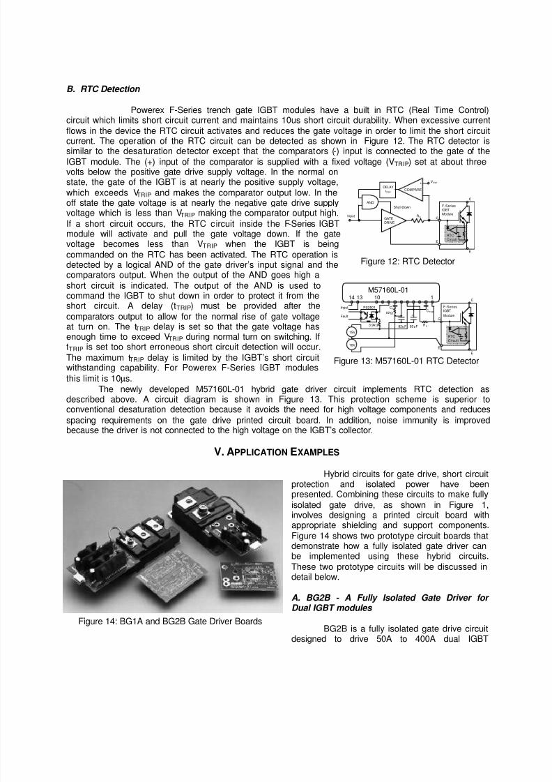
B. RTC Detection
Powerex F-Series trench gate IGBT modules have a built in RTC (Real Time Control)circuit which limits short circuit current and maintains 10us short circuit durability. When excessive current
flows in the device the RTC circuit activates and reduces the gate voltage in order to limit the short circuitcurrent. The operation of the RTC circuit can be detected as shown in Figure 12. The RTC detector issimilar to the desaturation detector except that the comparators (-) input is connected to the gate of the
IGBT module. The (+) input of the comparator is supplied with a fixed voltage (V TRIP) set at about threevolts below the positive gate drive supply voltage. In the normal onstate, the gate of the IGBT is at nearly the positive supply voltage,
which exceeds VTRIP and makes the comparator output low. In theoff state the gate voltage is at nearly the negative gate drive supplyvoltage which is less than VTRIP making the comparator output high.
If a short circuit occurs, the RTC circuit inside the F-Series IGBTmodule will activate and pull the gate voltage down. If the gatevoltage becomes less than VTRIP when the IGBT is being
commanded on the RTC has been activated. The RTC operation isdetected by a logical AND of the gate driver’s input signal and the
comparators output. When the output of the AND goes high ashort circuit is indicated. The output of the AND is used tocommand the IGBT to shut down in order to protect it from theshort circuit. A delay (t TRIP) must be provided after the
comparators output to allow for the normal rise of gate voltageat turn on. The tTRIP delay is set so that the gate voltage hasenough time to exceed VTRIP during normal turn on switching. IftTRIP is set too short erroneous short circuit detection will occur.
The maximum tTRIP delay is limited by the IGBT’s short circuitwithstanding capability. For Powerex F-Series IGBT modules
this limit is 10µs.
The newly developed M57160L-01 hybrid gate driver circuit implements RTC detection asdescribed above. A circuit diagram is shown in Figure 13. This protection scheme is superior to
conventional desaturation detection because it avoids the need for high voltage components and reducesspacing requirements on the gate drive printed circuit board. In addition, noise immunity is improvedbecause the driver is not connected to the high voltage on the IGBT’s collector.
V. APPLICATION EXAMPLES
Hybrid circuits for gate drive, short circuitprotection and isolated power have beenpresented. Combining these circuits to make fully
isolated gate drive, as shown in Figure 1,involves designing a printed circuit board withappropriate shielding and support components.
Figure 14 shows two prototype circuit boards that
demonstrate how a fully isolated gate driver canbe implemented using these hybrid circuits.
These two prototype circuits will be discussed indetail below.
A. BG2B - A Fully Isolated Gate Driver for Dual IGBT modules
BG2B is a fully isolated gate drive circuitdesigned to drive 50A to 400A dual IGBT
VTRIP
RTC
Circuit
C
E
G
+
F-SeriesIGBT
Module
E
COMPARE DELAY
tTRIP
GATEDRIVE
AND
RG
+
Shut-Down
Input
Figure 12: RTC Detector
1101314
M57160L-01
+
+
CTRIP
82µF RG 3.9kΩ
CSPS2501
82µF
15V
10V
+
+
Fault
Input
RTCCircuit
C
E
G
+
F-SeriesIGBT
Module
E
62Ω
Figure 13: M57160L-01 RTC Detector
Figure 14: BG1A and BG2B Gate Driver Boards

8/8/2019 gate dri
http://slidepdf.com/reader/full/gate-dri 8/10
modules. A pair of POWEREX M57159L-01, M57959L-01, M57962L/CL or M57160L-01 supply gate drivedepending on the application requirements. A pair of onboard M57145L-01 regulated DC to DC converterssupply isolated +15.8/-8.2V power for the gate drivers. Control on/off signals are optically isolated using
the hybrid gate drivers built in optocoupler.Optocouplers are also provided to isolate the faultfeedback signal. All isolation is designed for a
minimum 2500VRMS between the input and output.Figure 15 shows the full schematic for the BG2B gatedrive board. The jumpers (J1,J2) allow the board to
accept both desaturation detectors and the RTCdetector M57160-01 by connecting the detect pin (pin1) of the hybrid gate driver to the gate of the IGBT
module. The fault outputs of the two gate drives arecombined in to a single fault signal that will pull low ifeither gate driver detects a short circuit.
Figure 16 shows the circuit board layout forthe BG2B. The driver board has been designed tomount directly to the 0.110” gate and auxiliary emitter
terminals on the IGBT module. A universal holepattern allows the gate driver to fit all Powerex U-
Series and F-Series IGBT modules. Table 2 providesguidance for selecting components to populate theboard. Of particular importance is the selection of theelectrolytic power supply decoupling capacitors C1-C6.
These must be low impedance type in order to get goodpeak gate currents. It is generally advisable to use long life
1101314
13811
M57145L-01
+
+
C
C
DZ3
DZ1
DZ2
RG1
C4
+ R
R
C
OP1
IGBTModul
C
C2E1
G
E1
E2
G2
E21101314
M57959L/M57962L/M57160
13811
M57145L-01
+
+
C
C
D
DZ6
DZ4
DZ5
RG
C8
+ R
C
OP2
D
CN1
+VL
IN2
FO
+VS
GND
IN1
J2
D
D
CN2
J1
M57959L/M57962L/M57160
1
Figure 15: Schematic of BG2B Driver Board
Figure 16: BG2B Printed Circuit Layout
Table2: BG2B Component SelectionGuide
Designation Description Value ExampleType
C1, C2, C5, C6 Power supply decoupling
capacitors. Lowimpedance long life type.
82µF
35V
Panasonic FC
EEUFC1V820
C4, C8 DC to DC converter inputdecoupling capacitor.Low impedance long life
type
150µF
35V
Panasonic FCEEUFC1V151
C3, C7 Optional - Foradjustment of shortcircuit protection triptime.
0 to 10nF50V
muRata RPESeries
R1, R2 Current limit for faultopto
4.7K .25W
R3 Pull up for fault output 4.7K .25W
RG1, RG2 Series gate resistor -See Powerex IGBT
application notes
3Ù to 100Ù
0.5W to 1W
D1, D2, D3, D4 Collector voltagedetection diodes. Vrrmgreater than IGBT Vcesrating.
1A, 1000Vtrr<100ns
MotorolaMUR1100E
DZ1, DZ2, DZ4,DZ5
Gate protection zeners 17V, 0.5W 1N5247
DZ3, DZ6 Detect pin protectionzener
30V, 0.5W 1N5256
OP1, OP2 Opto for fault signal
isolation
NEC PS2501
CN1 MTA100 6 position rightangle header withlocking ramp
AMP640457-6
CN2 1/4” Ring Lug on 2” Wire AMP 34151
J1, J2 Insert when usingM57160L-01 with F-Series IGBT modulesand omit D1–D4 andDZ1-DZ6

8/8/2019 gate dri
http://slidepdf.com/reader/full/gate-dri 9/10
types because of the high temperatures that are often present inpower electronic circuits.
Figure 17 shows a typical interface circuit for the BG2B
gate driver board. All pins on the 6 position MTA-100 connectorare electrically isolated from the IGBT module. +VL is normallyconnected to the 5V logic power supply. When the IN1 or IN2
inputs are pulled low approximately 15ma flows from the +5Vsupply through the optocoupler inside the hybrid gate drivers andthe respective IGBT gate drive goes to the on state. If a short
circuit fault occurs the FO will be pulled low by the opto-transistorand will remain low for a minimum of 1ms. To insure reliable noise free operation an RC filter with a time
constant of approximately 10µs should be connected to the FO output as shown in figure 17. The +Vs pin
must be supplied with 12V to 18V DC to provide powerfor the onboard DC to DC converters. If multiple driverboards are used in a system they can all be powered
from a single 12V to 18V power supply.
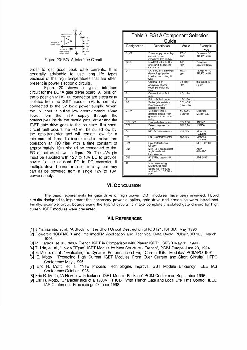
B. BG1A – A Fully Isolated Gate Driver for Large
Single IGBT Modules
BG1A is a fully isolated gate drive circuitdesigned to drive high current single IGBT modules.Gate drive is supplied by a Powerex M57962L/AL or anM57160L-01 hybrid gate driver with a complementary
emitter follower power booster. The circuit can deliver up to20A peak for efficient switching of modules rated up to 1200A.
The onboard M57145L-01 regulated DC to DC convertersupplies isolated power for the hybrid gate driver. With aninput of 12V to 18V DC the converter provides a +15.8/-8.2V
output with 2500VRMS isolation. The control on/off signal isoptically isolated using the hybrid gate drivers built inoptocoupler. An optocoupler is also provided to isolate the
fault feedback signal. All isolation is designed for a minimum
2500VRMS between the input and output.Figure 18 shows the full schematic for the BG1A gate
drive board. The jumper (J1) allows the board to accept bothdesaturation detectors and the RTC detector M57160-01 byconnecting the detect pin (pin 1) of the hybrid gate driver to
the gate of the IGBT module. A complementary emitterfollower output stage boosts the output current of the hybridgate driver to provide efficient drive for IGBT modules with
very large input capacitance. The isolated power supply hasbeen decoupled with both low impedance electrolytics and
1µF satcked film capacitors in order to minimize the
impedance to the IGBT gate.Figure 19 shows the circuit board layout for the
BG1A. The driver board has been designed to mount directlyto the gate and auxiliary emitter screw terminals on largesingle IGBT modules. A universal hole pattern allows the gatedriver to fit all Powerex U-Series and F-Series single IGBT
modules as well as 800A, 1000A and 1200A H-Seriesmodules. Table 3 provides guidance for selecting componentsto populate the board. Of particular importance is the
selection of the electrolytic power supply decouplingcapacitors C1 an C2. These must be low impedance type in
CN1
+VL
IN2
IN1
FO
+VS
GND
+5V+12 to+18V
Open Collector
Buffer/Driver
To logic levelcontrol circuits
RC Filter toremove noiseon fault signal
1
Figure 17: BG2B Interface Circuit
Figure 18: Schematic of BG1A Driver Board
1101314M57962L/M57160
13811
M57145L-
+
+
C
C
C
C
Q
Q
D
D
DZ3
DZ1
DZ2
C
RG
+
R
R
C
CN1
CN2
+VL
I
NC
FO
+VS
GND
IGBTModul
C
E
G
E
OP1 J1
1
Figure 19: BG1A Printed Circuit Layout
8/8/2019 gate dri
http://slidepdf.com/reader/full/gate-dri 10/10
order to get good peak gate currents. It isgenerally advisable to use long life typesbecause of the high temperatures that are often
present in power electronic circuits.Figure 20 shows a typical interface
circuit for the BG1A gate driver board. All pins on
the 6 position MTA-100 connector are electricallyisolated from the IGBT module. +VL is normallyconnected to the 5V logic power supply. When
the IN input is pulled low approximately 15maflows from the +5V supply through theoptocoupler inside the hybrid gate driver and the
IGBT gate drive goes to the on state. If a shortcircuit fault occurs the FO will be pulled low bythe opto-transistor and will remain low for a
minimum of 1ms. To insure reliable noise freeoperation an RC filter with a time constant of
approximately 10µs should be connected to the
FO output as shown in figure 20. The +Vs pinmust be supplied with 12V to 18V DC to providepower for the onboard DC to DC converter. If
multiple driver boards are used in a system theycan all be powered from a single 12V to 18Vpower supply.
VI. CONCLUSION
The basic requirements for gate drive of high power IGBT modules have been reviewed. Hybridcircuits designed to implement the necessary power supplies, gate drive and protection were introduced.Finally, example circuit boards using the hybrid circuits to make completely isolated gate drivers for high
current IGBT modules were presented.
VII. REFERENCES
[1] J Yamashita, et al. "A Study on the Short Circuit Destruction of IGBTs" , ISPSD, May 1993
[2] Powerex "IGBTMOD and IntellimodTM Application and Technical Data Book" PUB# 9DB-100, March1998
[3] M. Harada, et. al., "600v Trench IGBT in Comparison with Planar IGBT", ISPSD May 31, 1994
[4] T. Iida, et. al., "Low VCE(sat) IGBT Module by New Structure - Trench", PCIM Europe June 28, 1994[5] E. Motto, et. al., "Evaluating the Dynamic Performance of High Current IGBT Modules" PCIM/PQ 1994[6] E. Motto "Protecting High Current IGBT Modules From Over Current and Short Circuits" HFPC
Conference May ,1995[7] Eric R. Motto, et. al. “New Process Technologies Improve IGBT Module Efficiency” IEEE IAS
Conference October 1995
[8] Eric R. Motto, “A New Low Inductance IGBT Module Package” PCIM Conference September 1996[9] Eric R. Motto, “Characteristics of a 1200V PT IGBT With Trench Gate and Local Life Time Control” IEEE
IAS Conference Proceedings October 1998
Table 3: BG1A Component SelectionGuide
Designation Description Value ExampleType
C1,C2 Power supply decoupling
capacitors. Lowimpedance long life type.
150µF
35V
Panasonic FC
EEUFC1V151
C3,C4 Low ESR polyester filmor ceramic decouplingcapacitors
1µF50V
PanasonicECQV1H105JL
C5 DC to DC converter inputdecoupling capacitor.Low impedance long lifetype
150µF
35V
Panasonic FCEEUFC1V151
C6 Optional - For
adjustment of shortcircuit protection triptime.
0 to 10nF
50V
muRata RPE
Series
R1 Current limit for faultopto
4.7K .25W
R2 Pull up for fault output 4.7K .25W
RG Series gate resistor -See Powerex IGBTapplication notes
0.5Ù to 33Ù
0.5W to 2W
D1, D2 Collector voltage
detection diodes. Vrrmgreater than IGBT Vcesrating.
1A, 1000V
trr<100ns
Motorola
MUR1100E
DZ1, DZ2 Gate protection zeners 17V, 0.5W 1N5247DZ3 Detect pin protection
zener
30V, 0.5W 1N5256
Q1 NPN Booster transistor 15A, 80V MotorolaD44VH10
Q2 PNP Booster transistor 15A, 80V MotorolaD45VH10
OP1 Opto for fault signalisolation
NEC PS2501
CN1 MTA100 6 position rightangle header withlocking ramp
AMP640457-6
CN2 5/16” Ring Lug on 3.5”wire
AMP 34151
J1 Insert when usingM57160L-01 with F-Series IGBT modulesand omit D1, D2, DZ1-DZ3
CN1
+VL
IN
NC
FO
+VS
GND
+5V+12 to+18V
Open CollectorBuffer/Driver
To logic levelcontrol circuits
RC Filter toremove noiseon fault signal
1
Figure 20: BG1A Interface Circuit