Embed Size (px)
Citation preview
G3R75MT12D1200 V 75 mΩ SiC MOSFET
TM
Silicon Carbide MOSFETN-Channel Enhancement Mode
V = 1200 VR = 75 mΩI = 26 A
Features
• G3R™ Technology with +15 V Gate Drive • Softer R v/s Temperature Dependency • LoRing™ - Electromagnetically Optimized Design • Smaller R and Lower Q • Low Device Capacitances (C , C ) • Superior Cost-Performance Index • Robust Body Diode with Low V and Low Q • 100% Avalanche (UIL) Tested
Package
D = DrainG = GateS = Source
D
S
GRoHS
REACHTO-247-3
Advantages
• Compatible with Commercial Gate Drivers • Low Conduction Losses at all Temperatures • Reduced Ringing • Faster and More Efficient Switching • Lesser Switching Spikes and Lower Losses • Better Power Density and System Efficiency • Ease of Paralleling without Thermal Runaway • Superior Robustness and System Reliability
Applications
• Solar Inverters • EV/HEV Charging • UPS • High Voltage DC-DC Converters • Switched Mode Power Supplies • Motor Drives • Smart Grid Transmission and Distribution • Induction Heating and Welding
Absolute Maximum Ratings (At T = 25°C Unless Otherwise Stated)
Parameter Symbol Conditions Values Unit Note Drain-Source Voltage V V = 0 V, I = 100 µA 1200 V Gate-Source Voltage (Dynamic) V -10 / +20 V Gate-Source Voltage (Static) V Recommended Operation -5 / +15 V
Continuous Forward Current I T = 25°C, V = -5 / +15 V 36
A Fig. 15 T = 100°C, V = -5 / +15 V 26 T = 135°C, V = -5 / +15 V 19
Pulsed Drain Current I t ≤ 3µs, D ≤ 1%, V = 15 V, Note 1 70 A Fig. 14 Power Dissipation P T = 25°C 182 W Fig. 16 Non-Repetitive Avalanche Energy E L = 4.0 mH, I = 10.0 A 199 mJ Operating and Storage Temperature T , T -55 to 175 °C
Thermal/Package Characteristics
Parameter Symbol Conditions Values
Unit Note Min. Typ. Max.
Thermal Resistance, Junction - Case R 0.63 0.82 °C/W Fig. 13 Weight W 6.1 g Mounting Torque T Screws to Heatsink 1.1 Nm
Note 1: Pulse Width t Limited by T
DS
DS(ON)(Typ.)
D (T = 100°C)C
DS(ON)
G(INT) G
OSS RSS
F RR
C
DS(max) GS D
GS(max)
GS(op)
D
C GS
C GS
C GS
D(pulse) P GS
D c
AS AS
j stg
thJC
T
M
P j(max)
Rev 21/May Latest Version at: www.genesicsemi.com/sic-mosfet/G3R75MT12D/G3R75MT12D.pdf Page 1 of 14
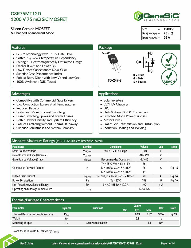
G3R75MT12D1200 V 75 mΩ SiC MOSFET
TM
Electrical Characteristics (At T = 25°C Unless Otherwise Stated)
Parameter Symbol Conditions Values
Unit Note Min. Typ. Max.
Drain-Source Breakdown Voltage V V = 0 V, I = 100 µA 1200 V Zero Gate Voltage Drain Current I V = 1200 V, V = 0 V 1 µA
Gate Source Leakage Current I V = 0 V, V = 20 V 100
nA V = 0 V, V = -10 V -100
Gate Threshold Voltage V V = V , I = 10.0 mA 1.8 2.70
V Fig. 9 V = V , I = 10.0 mA, T = 175°C 2.05
Transconductance g V = 10 V, I = 20 A 9.0
S Fig. 4 V = 10 V, I = 20 A, T = 175°C 10.1
Drain-Source On-State Resistance R V = 15 V, I = 20 A 75 97
mΩ Fig. 5-8 V = 15 V, I = 20 A, T = 175°C 106
Input Capacitance C
V = 800 V, V = 0 V f = 1 MHz, V = 25mV
1545 pF Fig. 11 Output Capacitance C 46
Reverse Transfer Capacitance C 3.8 C Stored Energy E 18 µJ Fig. 12 C Stored Charge Q 68 nC Effective Output Capacitance (EnergyRelated)
C 56 pF Note 2
Effective Output Capacitance (TimeRelated)
C 85
Gate-Source Charge Q V = 800 V, V = -5 / +15 V I = 20 A
Per IEC607478-4
15 nC Fig. 10 Gate-Drain Charge Q 16
Total Gate Charge Q 47 Internal Gate Resistance R f = 1 MHz, V = 25 mV 1.3 Ω Turn-On Switching Energy(Body Diode)
E T = 25°C, V = -5/+15V, R = 8 Ω, L =
80.0 µH, I = 20 A, V = 800 V
217 µJ Fig. 22,26
Turn-Off Switching Energy(Body Diode)
E 52
Turn-On Delay Time t V = 800 V, V = -5/+15V
R = 8 Ω, L = 80.0 µH, I = 20 ATiming relative to V , Inductive load
39
ns Fig. 24 Rise Time t 15 Turn-Off Delay Time t 18 Fall Time t 10
*The chip technology was characterized up to 200 V/ns. The measured dV/dt was limited by measurement test setup and package.Note 2: C , a lumped capacitance that gives same stored energy as C while V is rising from 0 to 800V.
C , a lumped capacitance that gives same charging times as C while V is rising from 0 to 800V.
C
DSS GS D
DSS DS GS
GSSDS GS
DS GS
GS(th)DS GS D
DS GS D j
fsDS D
DS D j
DS(ON)GS D
GS D j
iss
DS GS
AC
oss
rss
oss oss
oss oss
o(er)
o(tr)
gs DS GS
Dgd
g
G(int) AC
Onj GS G(ext)
D DDOff
d(on)DD GS
G(ext) D
DS
r
d(off)
f
o(er) OSS DS
o(tr) OSS DS
Rev 21/May Latest Version at: www.genesicsemi.com/sic-mosfet/G3R75MT12D/G3R75MT12D.pdf Page 2 of 14
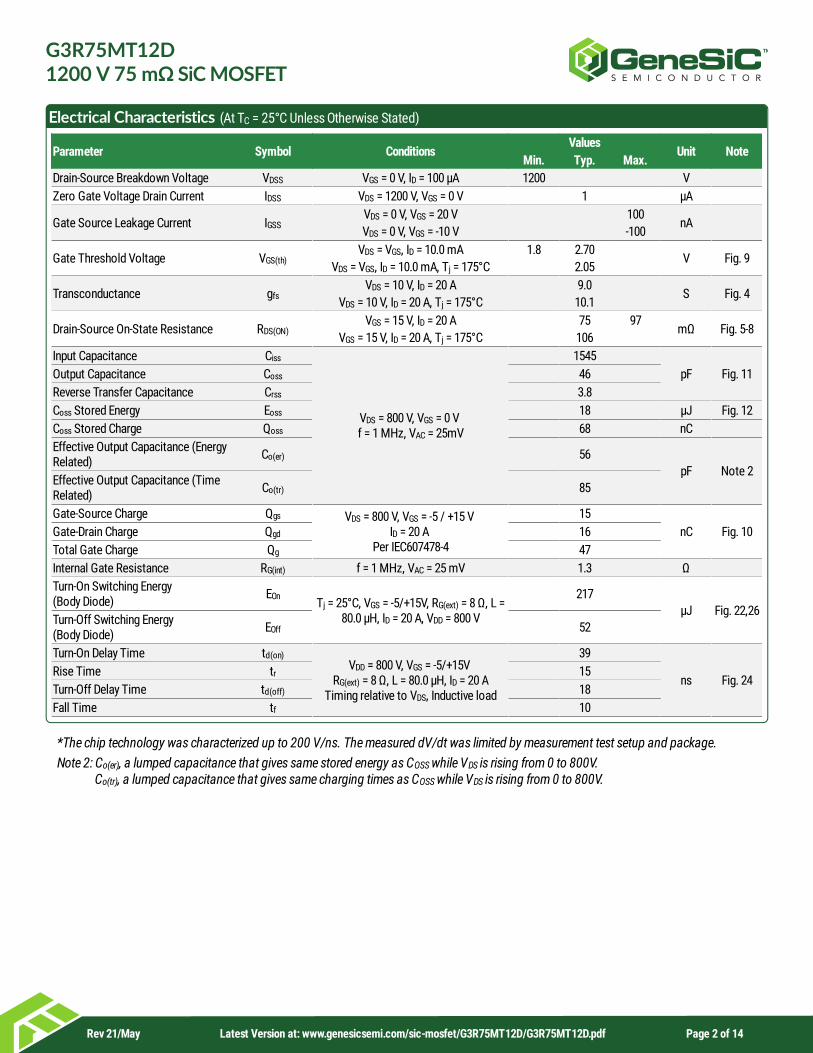
G3R75MT12D1200 V 75 mΩ SiC MOSFET
TM
Reverse Diode Characteristics
Parameter Symbol Conditions Values
Unit Note Min. Typ. Max.
Diode Forward Voltage V V = -5 V, I = 10 A 4.9
V Fig. 17-18 V = -5 V, I = 10 A, T = 175°C 4.4
Continuous Diode Forward Current I V = -5 V, T = 100°C 16 A Diode Pulse Current I V = -5 V, Note 1 64 A Reverse Recovery Time t
V = -5 V, I = 20 A, V = 800 Vdif/dt = 1200 A/µs, T = 25°C
15 ns Reverse Recovery Charge Q 64 nC Peak Reverse Recovery Current I 4 A Reverse Recovery Time t
V = -5 V, I = 20 A, V = 800 Vdif/dt = 1200 A/µs, T = 175°C
23 ns Reverse Recovery Charge Q 160 nC Peak Reverse Recovery Current I 7 A
SDGS SD
GS SD j
S GS c
S(pulse) GS
rrGS SD R
jrr
rrm
rrGS SD R
jrr
rrm
Rev 21/May Latest Version at: www.genesicsemi.com/sic-mosfet/G3R75MT12D/G3R75MT12D.pdf Page 3 of 14
G3R75MT12D1200 V 75 mΩ SiC MOSFET
TM
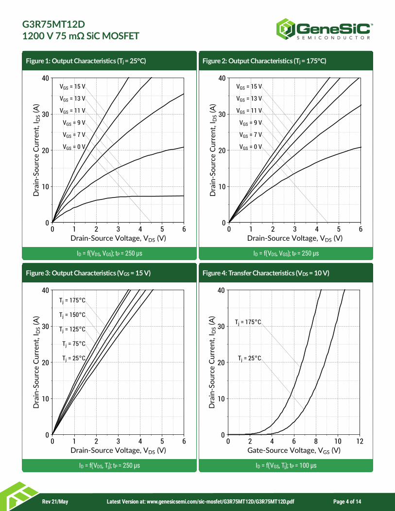
Figure 1: Output Characteristics (T = 25°C)
I = f(V , V ); t = 250 µs
Figure 2: Output Characteristics (T = 175°C)
I = f(V , V ); t = 250 µs
Figure 3: Output Characteristics (V = 15 V)
I = f(V , T); t = 250 µs
Figure 4: Transfer Characteristics (V = 10 V)
I = f(V , T); t = 100 µs
j
D DS GS P
j
D DS GS P
GS
D DS j P
DS
D GS j P
Rev 21/May Latest Version at: www.genesicsemi.com/sic-mosfet/G3R75MT12D/G3R75MT12D.pdf Page 4 of 14
G3R75MT12D1200 V 75 mΩ SiC MOSFET
TM
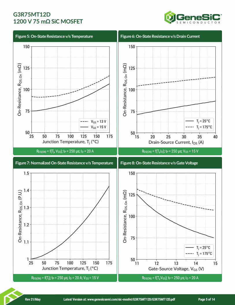
Figure 5: On-State Resistance v/s Temperature
R = f(T, V ); t = 250 µs; I = 20 A
Figure 6: On-State Resistance v/s Drain Current
R = f(T,I ); t = 250 µs; V = 15 V
Figure 7: Normalized On-State Resistance v/s Temperature
R = f(T); t = 250 µs; I = 20 A; V = 15 V
Figure 8: On-State Resistance v/s Gate Voltage
R = f(T,V ); t = 250 µs; I = 20 A
DS(ON) j GS P D DS(ON) j D P GS
DS(ON) j P D GS DS(ON) j GS P D
Rev 21/May Latest Version at: www.genesicsemi.com/sic-mosfet/G3R75MT12D/G3R75MT12D.pdf Page 5 of 14
G3R75MT12D1200 V 75 mΩ SiC MOSFET
TM
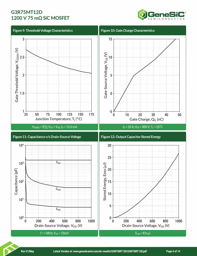
Figure 9: Threshold Voltage Characteristics
V = f(T); V = V ; I = 10.0 mA
Figure 10: Gate Charge Characteristics
I = 20 A; V = 800 V; T = 25°C
Figure 11: Capacitance v/s Drain-Source Voltage
f = 1 MHz; V = 25mV
Figure 12: Output Capacitor Stored Energy
E = f(V )
GS(th) j DS GS D D DS c
AC oss DS
Rev 21/May Latest Version at: www.genesicsemi.com/sic-mosfet/G3R75MT12D/G3R75MT12D.pdf Page 6 of 14
G3R75MT12D1200 V 75 mΩ SiC MOSFET
TM
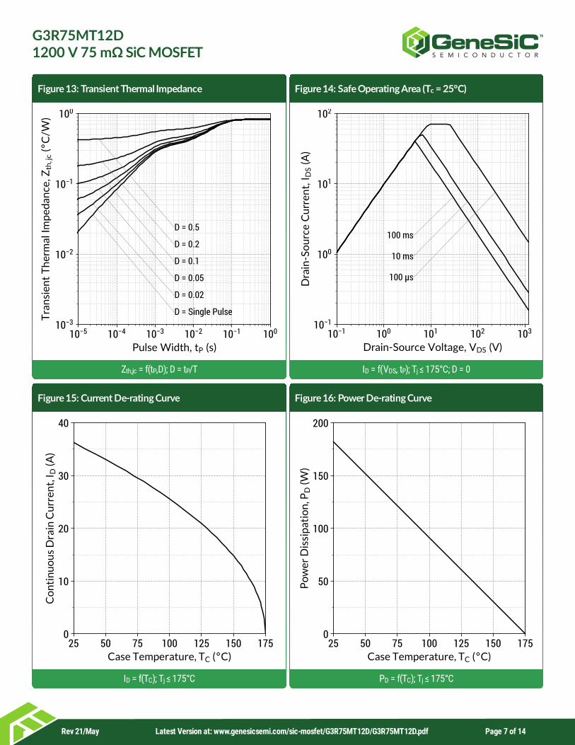
Figure 13: Transient Thermal Impedance
Z = f(t ,D); D = t /T
Figure 14: Safe Operating Area (T = 25°C)
I = f(V , t ); T ≤ 175°C; D = 0
Figure 15: Current De-rating Curve
I = f(T ); T ≤ 175°C
Figure 16: Power De-rating Curve
P = f(T ); T ≤ 175°C
th,jc P P
c
D DS P j
D C j D C j
Rev 21/May Latest Version at: www.genesicsemi.com/sic-mosfet/G3R75MT12D/G3R75MT12D.pdf Page 7 of 14
G3R75MT12D1200 V 75 mΩ SiC MOSFET
TM
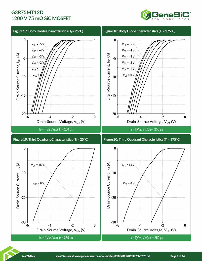
Figure 17: Body Diode Characteristics (T = 25°C)
I = f(V , V ); t = 250 µs
Figure 18: Body Diode Characteristics (T = 175°C)
I = f(V , V ); t = 250 µs
Figure 19: Third Quadrant Characteristics (T = 25°C)
I = f(V , V ); t = 250 µs
Figure 20: Third Quadrant Characteristics (T = 175°C)
I = f(V , V ); t = 250 µs
j
D DS GS P
j
D DS GS P
j
D DS GS P
j
D DS GS P
Rev 21/May Latest Version at: www.genesicsemi.com/sic-mosfet/G3R75MT12D/G3R75MT12D.pdf Page 8 of 14
G3R75MT12D1200 V 75 mΩ SiC MOSFET
TM
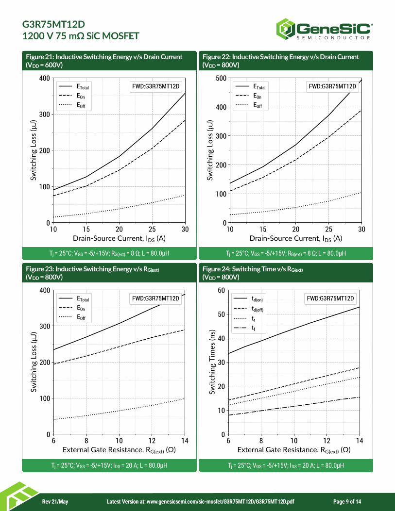
Figure 21: Inductive Switching Energy v/s Drain Current(V = 600V)
T = 25°C; V = -5/+15V; R = 8 Ω; L = 80.0µH
Figure 22: Inductive Switching Energy v/s Drain Current(V = 800V)
T = 25°C; V = -5/+15V; R = 8 Ω; L = 80.0µH
Figure 23: Inductive Switching Energy v/s R(V = 800V)
T = 25°C; V = -5/+15V; I = 20 A; L = 80.0µH
Figure 24: Switching Time v/s R(V = 800V)
T = 25°C; V = -5/+15V; I = 20 A; L = 80.0µH
DD
j GS G(ext)
DD
j GS G(ext)
G(ext)
DD
j GS DS
G(ext)
DD
j GS DS
Rev 21/May Latest Version at: www.genesicsemi.com/sic-mosfet/G3R75MT12D/G3R75MT12D.pdf Page 9 of 14
G3R75MT12D1200 V 75 mΩ SiC MOSFET
TM
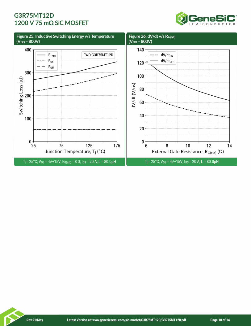
Figure 25: Inductive Switching Energy v/s Temperature(V = 800V)
T = 25°C; V = -5/+15V; R = 8 Ω; I = 20 A; L = 80.0µH
Figure 26: dV/dt v/s R(V = 800V)
T = 25°C; V = -5/+15V; I = 20 A; L = 80.0µH
DD
j GS G(ext) DS
G(ext)
DD
j GS DS
Rev 21/May Latest Version at: www.genesicsemi.com/sic-mosfet/G3R75MT12D/G3R75MT12D.pdf Page 10 of 14
G3R75MT12D1200 V 75 mΩ SiC MOSFET
TM
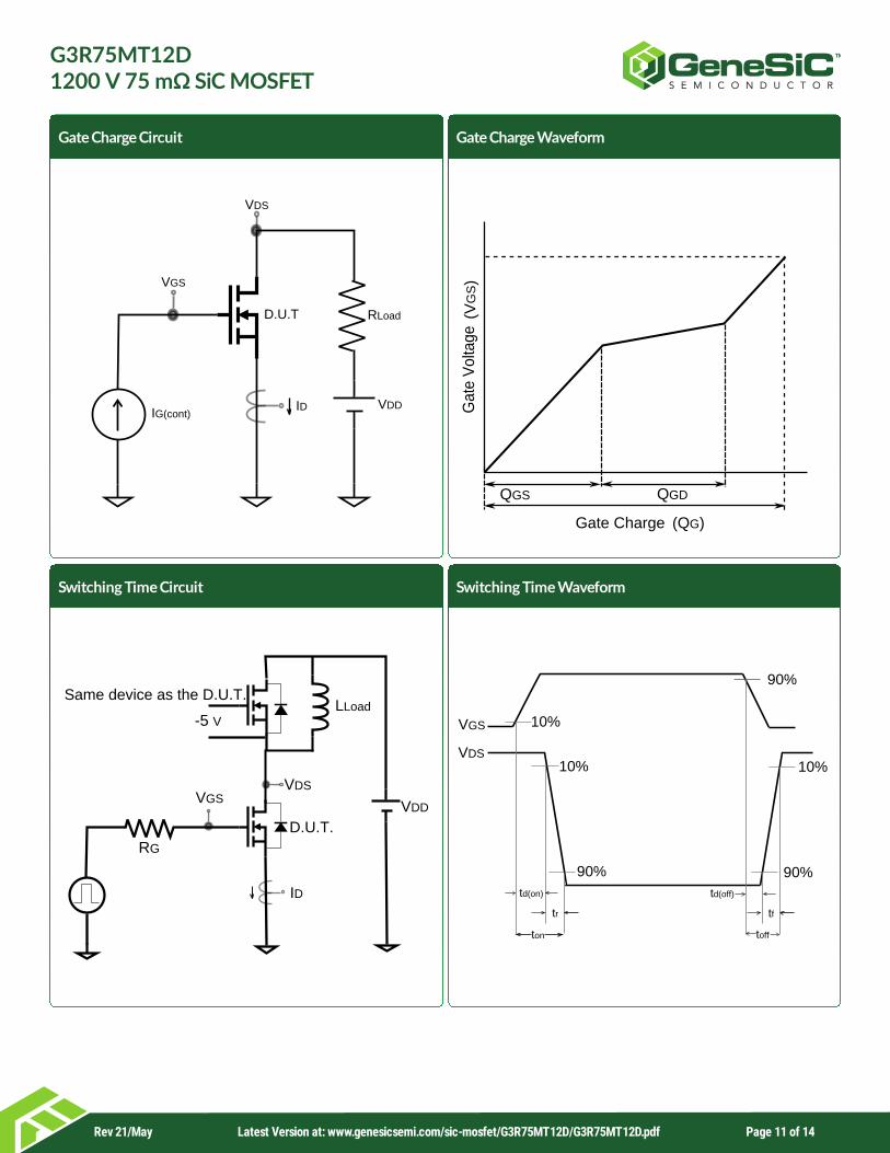
Gate Charge Circuit
VGS
IG(cont) ID VDD
RLoadD.U.T
VDS
Gate Charge Waveform
(VGS)
GateVoltage
QGS QGD
(QG)Gate Charge
Switching Time Circuit
ID
VGS
D.U.T.
VDS
LLoad
VDD
Same device as the D.U.T.
RG
-5 V
Switching Time Waveform
10%
90%
10% 10%
90% 90%td(on)
VGS
VDS
tr
ton
td(off)
tf
toff
Rev 21/May Latest Version at: www.genesicsemi.com/sic-mosfet/G3R75MT12D/G3R75MT12D.pdf Page 11 of 14
G3R75MT12D1200 V 75 mΩ SiC MOSFET
TM
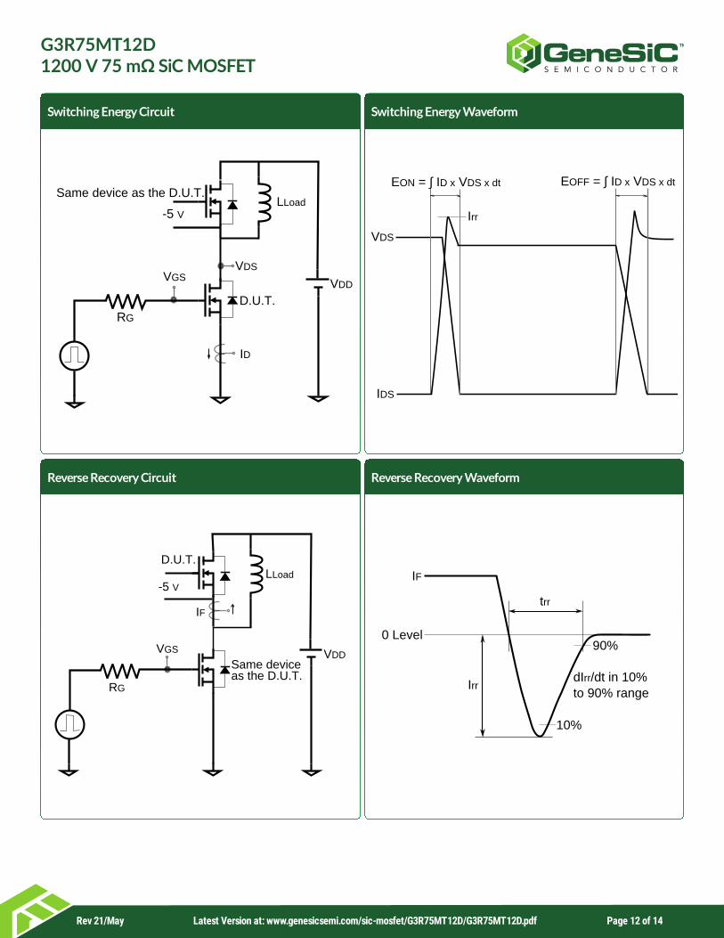
Switching Energy Circuit
ID
VGS
D.U.T.
VDS
LLoad
VDD
Same device as the D.U.T.
RG
-5 V
Switching Energy Waveform
VDS
Irr
EON = ∫ ID x VDS x dt
IDS
EOFF = ∫ ID x VDS x dt
Reverse Recovery Circuit
VGS
D.U.T.LLoad
VDDSame device
RG
IF
as the D.U.T.
-5 V
Reverse Recovery Waveform
trr
Irr
10%
90%
IF
0 Level
dIrr/dt in 10%to 90% range
Rev 21/May Latest Version at: www.genesicsemi.com/sic-mosfet/G3R75MT12D/G3R75MT12D.pdf Page 12 of 14
G3R75MT12D1200 V 75 mΩ SiC MOSFET
TM
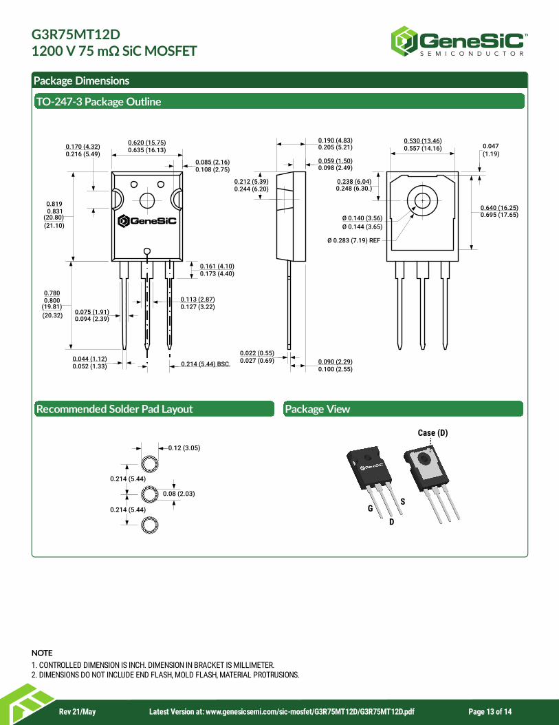
Package Dimensions
TO-247-3 Package Outline
Ø 0.140 (3.56)Ø 0.144 (3.65)
0.075 (1.91)0.094 (2.39)
0.044 (1.12)0.052 (1.33) 0.214 (5.44) BSC.
0.022 (0.55)0.027 (0.69)
0.059 (1.50)0.098 (2.49)
0.190 (4.83)0.205 (5.21)
0.090 (2.29)0.100 (2.55)
0.170 (4.32)0.216 (5.49)
0.8190.831
(21.10)
0.7800.800
(20.32)
0.161 (4.10)0.173 (4.40)
0.212 (5.39)0.244 (6.20)
Ø 0.283 (7.19) REF
0.640 (16.25)0.695 (17.65)
0.530 (13.46)0.557 (14.16) 0.047
0.113 (2.87)0.127 (3.22)
0.238 (6.04)0.248 (6.30.)
0.620 (15.75)0.635 (16.13)
0.085 (2.16)0.108 (2.75)
(1.19)
(20.80)
(19.81)
Recommended Solder Pad Layout
0.12 (3.05)
0.214 (5.44)
0.214 (5.44)
0.08 (2.03)
Package View
G
D
Case (D)
S
NOTE1. CONTROLLED DIMENSION IS INCH. DIMENSION IN BRACKET IS MILLIMETER.2. DIMENSIONS DO NOT INCLUDE END FLASH, MOLD FLASH, MATERIAL PROTRUSIONS.
Rev 21/May Latest Version at: www.genesicsemi.com/sic-mosfet/G3R75MT12D/G3R75MT12D.pdf Page 13 of 14
G3R75MT12D1200 V 75 mΩ SiC MOSFET
TM
ComplianceRoHS Compliance
The levels of RoHS restricted materials in this product are below the maximum concentration values (also referred to as the thresholdlimits) permitted for such substances, or are used in an exempted application, in accordance with EU Directive 2011/65/EC (RoHS 2), asadopted by EU member states on January 2, 2013 and amended on March 31, 2015 by EU Directive 2015/863. RoHS Declarations for thisproduct can be obtained from your GeneSiC representative.
REACH Compliance
REACH substances of high concern (SVHCs) information is available for this product. Since the European Chemical Agency (ECHA) haspublished notice of their intent to frequently revise the SVHC listing for the foreseeable future, please contact a GeneSiC representative toinsure you get the most up-to-date REACH SVHC Declaration. REACH banned substance information (REACH Article 67) is also availableupon request.
DisclaimerGeneSiC Semiconductor, Inc. reserves right to make changes to the product specifications and data in this document without notice.GeneSiC disclaims all and any warranty and liability arising out of use or application of any product. No license, express or implied to anyintellectual property rights is granted by this document.
Unless otherwise expressly indicated, GeneSiC products are not designed, tested or authorized for use in life-saving, medical, aircraftnavigation, communication, air traffic control and weapons systems, nor in applications where their failure may result in death, personalinjury and/or property damage.
Related Links• SPICE Models: https://www.genesicsemi.com/sic-mosfet/G3R75MT12D/G3R75MT12D_SPICE.zip• PLECS Models: https://www.genesicsemi.com/sic-mosfet/G3R75MT12D/G3R75MT12D_PLECS.zip• CAD Models: https://www.genesicsemi.com/sic-mosfet/G3R75MT12D/G3R75MT12D_3D.zip• Gate Driver Reference: https://www.genesicsemi.com/technical-support• Evaluation Boards: https://www.genesicsemi.com/technical-support• Reliability: https://www.genesicsemi.com/reliability• Compliance: https://www.genesicsemi.com/compliance• Quality Manual: https://www.genesicsemi.com/quality
Revision History• Rev 21/May: Updated switching time and switching energy data• Supersedes: Rev 20/Jun, Rev 20/Aug, Rev 21/Jan
www.genesicsemi.com/sic-mosfet/
Rev 21/May Published by GeneSiC Semiconductor, Inc.
Copyright© 2021 GeneSiC Semiconductor Inc. 43670 Trade Center Place Suite 155, Dulles, VA 20166; USA
All Rights Reserved. Page 14 of 14