Embed Size (px)
Citation preview

Future Trend of Materials for Advanced Semiconductor Manufacturing
Nobu KOSHIBA
Representative Director and President
1

• Future Trend of Semiconductor Devices
• Materials for Advanced Semiconductor
Manufacturing
− Lithography Materials
− Planarization and Cleaning Materials
− Packaging Materials
− Extension to Digital Medicine
• Summary
2
Contents

Progresses of SemiconductorYear ’14 ’16 ’18 ’20 ’22 ’24
Tech. node 20nm~14nm 10nm ~ 7nm ~ 5nm ~ 3nm ~ 2nm ~
Gate leng. (PR) 25 nm ~ 20 nm ~ 16 nm ~ 12 nm ~ 10 nm ~ 8 nm ~
Logic
Tech. trend
� 3D architecture
Flash
Tech. trend
� 3D integration
DRAM
Tech. trend
� wider bandwidth
Package
Planar FinFET
MOSFET
Si-Ge / III-V group Fin-FET
Wire
Wire bonding 3D NAND (48)
Band: 2.2Gbps
Wire bonding
Band: 3.2Gbps
Stack: 9 chips
TSVWire lessor optical connect?
non-MOSFET
non-charge
Band: 3.6Gbps
Stack: 13 chips
Band: 4.2Gbps
Stack: 17 chips
3D NAND (64)
3D NAND ( >100)
Emerging memory
WL-CSP
2.1D 2.5D
3D-WLP 3D w/ TSV
3
GAA
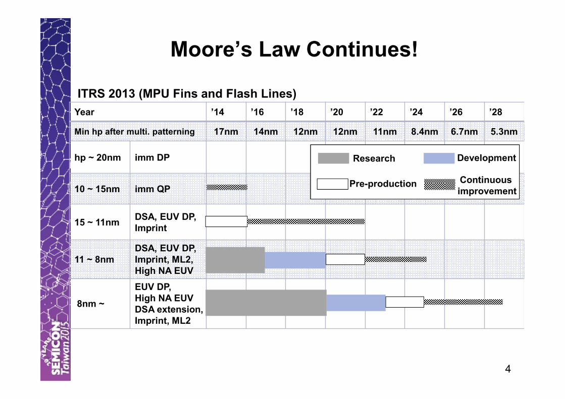
Moore’s Law Continues!
Year ’14 ’16 ’18 ’20 ’22 ’24 ’26 ’28
Min hp after multi. patterning 17nm 14nm 12nm 12nm 11nm 8.4nm 6.7nm 5.3nm
hp ~ 20nm imm DP
10 ~ 15nm imm QP
15 ~ 11nmDSA, EUV DP,
Imprint
11 ~ 8nm
DSA, EUV DP,
Imprint, ML2,
High NA EUV
8nm ~
EUV DP,
High NA EUV
DSA extension,
Imprint, ML2
ITRS 2013 (MPU Fins and Flash Lines)
Research Development
Pre-production Continuous
improvement
4

2007 40 nm LS, ArFi 2008 26 nm LS, ArFi DP 2010 19 nm LS, EUV
Photoresist Scaling
2015 13nm LS, EUV 9.5nm LS, DSA
� Continuous “Materials Innovation” of litho-chemistry extends
resolution limits5

EUV Resist Performance
LS Pattern
Exp. NXE3300B
Chemically Amplified Resist
Best in 2014
15nmLSBest in 2015
15nmLS
LWR: 5.9nm LWR: 5.3nmDose 40% down
New Platform
(Metal Resist)
24nmLS
24nmLS 24nmLS
CDU: 3.5nm CDU: 3.4nmDose 20% down
CH Pattern
Exp. NXE3100
� Chemically amplified photoresists made significant improvements
in photospeed while unconventional platforms appear to become a
viable option. 6

Patterned Area Open Area
190nm
45nm
Photo-Resist• Good LWR/CDU
• High resolution
Spin-on Inorg. ML• Resist compatibility
• High etch selectivity
Spin-on Org. UL• High etch selectivity
• Planarization
• Thermal Stability
Integrated Litho-solution for
Advanced Semiconductor Manufacturing
� Fully optimized and integrated litho-solution in conjunction
with low defect control to meet specific customers’ needs
through “Innovation One-on-One.”
7
+
Defect Control

ITRS 2012 (Yield Enhancement) 8

Comprehensive Supply Chain Control
� No compromise on integrity of raw materials supply in terms
of change control and materials quality profile.
� Semiconductor materials suppliers are the ones to bridge the
gap between semiconductor standards and (petro)chemical
industry’s common sense.
9
Semiconductor
Industry
(Petro)Chemical
Industry
Semiconductor Materials Suppliers

Year ’14 ’16 ’18 ’20 ’22 ’24
Tech. node 20nm~14nm 10nm ~ 7nm ~ 5nm ~ 3nm ~ 2nm ~
Gate leng. (PR) 25 nm ~ 20 nm ~ 16 nm ~ 12 nm ~ 10 nm ~ 8 nm ~
Logic
Tech. trend
� 3D architecture
New Materials
Gate
Metallization
Dielectrics
Zr, Hf
Cu,W
k=2.55
+TaN/Ta,Co
k=2.55-2.4
+Ru
k=2.4-2.2
Ge, In
+Mn
k=2.2-2.0
+Graphen
k<2.0
10
More New Materials to be introduced in Advanced Semiconductor Manufacturing
Planar FinFET
MOSFET
Si-Ge / III-V group Fin-FET
non-MOSFET
non-chargeGAA
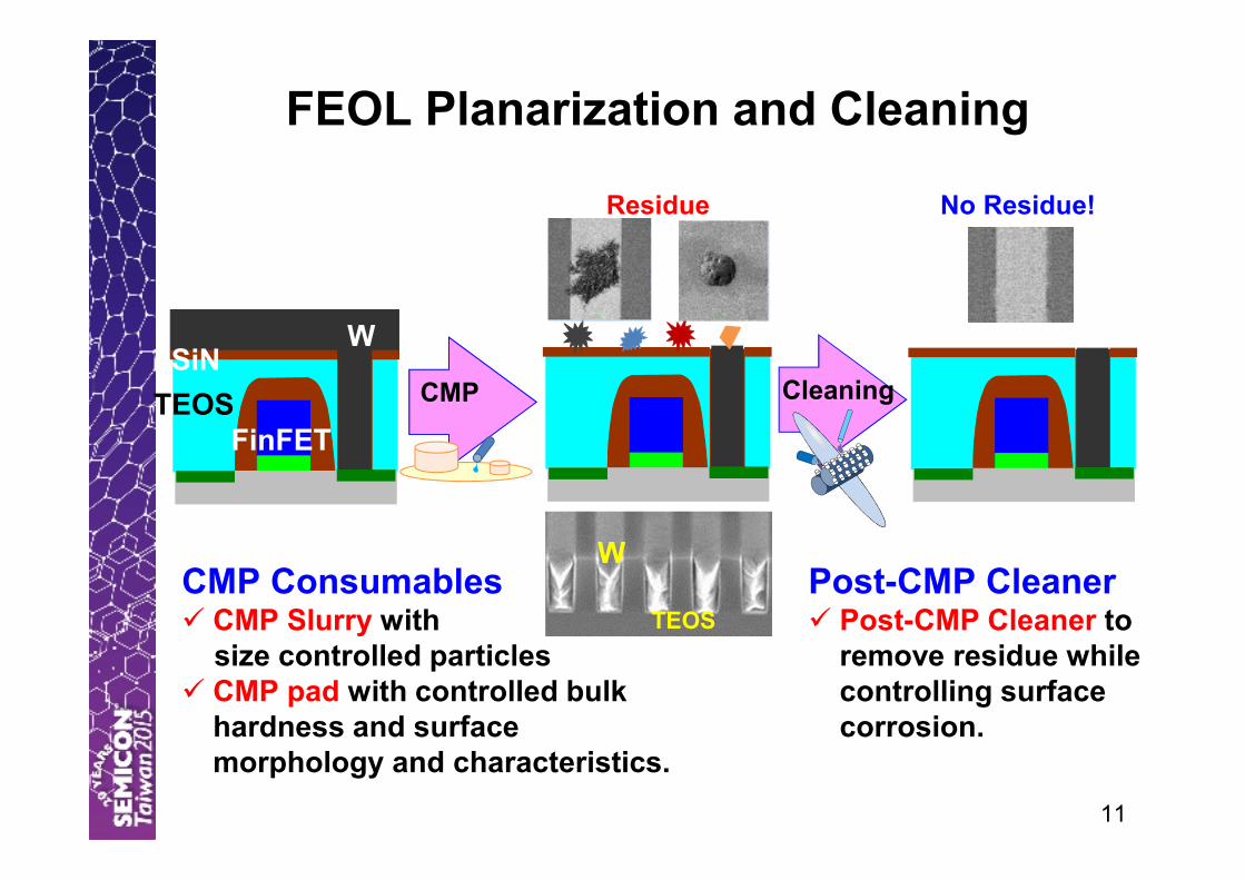
FEOL Planarization and Cleaning
CMP Consumables� CMP Slurry with
size controlled particles
� CMP pad with controlled bulk
hardness and surface
morphology and characteristics.
Post-CMP Cleaner� Post-CMP Cleaner to
remove residue while
controlling surface
corrosion.
CMP Cleaning
W
FinFET
TEOS
SiN
11
W
TEOS
Residue No Residue!

12
Advanced Slurry for III-V Materials
X-sec @ TEM
Applicable to Ge, InP & InGaAs
Extreme CMP
Rms < 0.5nmRms>20nm
Before CMP After CMP
� Good selectivity control and Rms less than 1nm after polish.
� No toxic gas generation during the polish process.
CMP
Surface Roughness Surface Roughness

Cu
NiCo
Cr
Al
Ag
Rh Ir Mo W
Ru
TaNb
Bu
lk r
esis
tivity (
mic
ro O
hm
cm
)
Melting Temperature (deg C)
Wire scaling
New Metallurgy in BEOL
� New metallurgy will be introduced into BEOL process.
13

Year ’14 ’16 ’18 ’20 ’22 ’24
Tech. node 20nm~14nm 10nm ~ 7nm ~ 5nm ~ 3nm ~ 2nm ~
Gate leng. (PR) 25 nm ~ 20 nm ~ 16 nm ~ 12 nm ~ 10 nm ~ 8 nm ~
Package
WL-CSP
2.1D 2.5D
3D-WLP 3D w/ TSV
Plating resist� High aspect for Cu-pillar
� High resolution for RDL
�Wide process margin
Dielectrics� Dielectric properties
� Mechanical strength
� Photo-definable
Temporary bonding for TSV� Satisfy adhesion and de-bonding
properties
� No damage on thinned wafer
Materials for new process� Lift-off
� Spin-on metal (Metal ink)
More than Moore!
14

Thick Resist for Metal Deposition
High Cu Pillar
(for Fan-out WLP)
� Extremely thick
(~200um)
� High photospeed
RDL
(for Fan-out WLP)
� High resolution
(<2um)
General Metal Depo.
(for Sputtering)
� Over-hung profile
� Save process cost
15
Photo-resist
MetalPattern
For Cu Plating
Cu plated Cu sputtered
3.4um 2um80um
Cu plated
For Lift-off

Digital Medicine: Emerging Need for
Bio-Compatible Materials
µ µ µ µ fluidic devicesInjection molding-R2R-...
Si-based devicesSemiconductor
Simple – Cheap- DisposableExpensive, high complexity
Low technological value
Integration of Si
components in plastic
microfluidic cartridge
Hybrid devices
High technological value
Key to success
Personalised Healthcare:
Lab-on-chip
Biggest MARKET share
Mainly chip in LABLimited commercialization
Key challenge = Packaging and Integration16

Implantation
Explantation
Collaboration with U. Ghent : Prof L. Vlaminck & Prof R. Cornelissen
Implantation of 3 copies of 8 different samples for 2 months
•White milk goat
•3 years old
•Anesthetized before operation
Tissue
with sample
in formalin
Si-chip
Material coated
Sample structure
17
How to confirm Bio-compatibility?

30µm
clean bond pad opening
No residues
29.3µm
Microfluidics
channel
Heater element
area
Basic material evaluation showed
•non-cytotoxic
•no unwanted interaction with biochemistry
•optical transparency / low out-gassing
•excellent resolution and patterning profile
18
PA (Photo-definable Adhesive)
for imec’s Cell Sorter
Courtesy of imec

• More and aggressive “Materials Innovation” is required to support advanced semiconductor manufacturing to enable Moore’s Law extension and More-than-Moore.
• “Innovation One-on-One” and “Comprehensive Supply Chain Control” are the keys-for-success to make 10nm advanced manufacturing and beyond commercially successful.
19
Summary