Embed Size (px)
Citation preview

Use of FTDI devices in life support and/or safety applications is entirely at the user’s risk, and the user agrees to defend, indemnify and hold harmless FTDI from any and all damages, claims, suits or expense resulting
from such use.
FT12 Series Evaluation Kit Datasheet Version 1.0
Document Reference No.: FT_000728 Clearance No.: FTDI# 314
Future Technology
Devices International Ltd
Datasheet
FT12 Series Evaluation Kit
Generic USB device development kit
1 Introduction
The FT12 series evaluation kit is used to develop and demonstrate functions of FTDI’s FT120, FT121 and FT122 ICs. The kit consists of a main board and one of the FT120/FT121/FT122 add-on
modules. These modules can provide a generic USB device function to a microcontroller(MCU) with the following interfaces:
- UMFT120DC: 8-bit 8051 interface, up to 3 bi-
directional endpoints
- UMFT121DC: SPI slave interface, up to 8 bi-
directional endpoints
- UMFT122DC: 8-bit 8051 interface, up to 8 bi-directional endpoints
1.1 Features
- Micro-B USB connector to connect to USB host or Charger port
- Allow bus-power or self-power configuration
- LPC1114 Cortex-M0 microcontroller for
easy software development
- Pushbutton and LEDs for HID
application
- In-system firmware upgradable
- On-board prototype area for application development
2 Ordering Information
Part No * Description
UMFT12XEV Main board for evaluating FT120, FT121 and FT122 add-on modules. Fitted
with LPC1114 Cortex-M0 MCU. Firmware upgradable with UART or SWD interface. Note: Board is shipped with firmware to support CDC class devices
pre-loaded
UMFT120DC FT120 add-on module. 8-bit 8051 parallel bus. 3 bi-directional endpoints. I/O level 3.3V (5V tolerant). Compatible to PDIUSBD12.
UMFT121DC FT121 add-on module. SPI slave bus. 8 bi-directional endpoints. I/O level 1.8/2.5/3.3V.
UMFT122DC FT122 add-on module. 8-bit 8051 parallel bus. 8 bi-directional endpoints. I/O level 1.8/2.5/3.3V.
* Note that PCB label may differ
Table 2-1 Ordering information

Copyright © 2012 Future Technology Devices International Limited 2
FT12 Series Evaluation Kit Datasheet Version 1.0
Document Reference No.: FT_000728 Clearance No.: FTDI# 314
Table of Contents
1 Introduction ................................................................................... 1
1.1 Features ........................................................................................................ 1
2 Ordering Information ..................................................................... 1
3 Hardware description ..................................................................... 3
3.1 UMFT12XEV Main Board ................................................................................ 3
3.2 UMFT120DC daughter board.......................................................................... 4
3.3 UMFT121DC daughter board.......................................................................... 6
3.4 UMFT122DC daughter board.......................................................................... 7
3.5 Accessories ................................................................................................... 8
4 Initial Board Set-up ...................................................................... 10
4.1 Installing UMFT12xDC daughter board ........................................................ 10
4.2 Set the jumpers........................................................................................... 10
4.3 Install the driver ......................................................................................... 11
5 Running demo tests ...................................................................... 16
5.1 Serial Loopback test .................................................................................... 16
5.2 USB Charger test ......................................................................................... 16
6 Board Circuit Schematics and BOMs ............................................. 18
6.1 UMFT12XEV Schematic and BOM ................................................................. 18
6.2 UMFT120DC Schematic and BOM ................................................................. 19
6.3 UMFT121DC Schematic and BOM ................................................................. 20
6.4 UMFT122DC Schematic and BOM ................................................................. 21
7 Firmware Upgrade Process ........................................................... 23
7.1 Put LPC1114 microcontroller in ISP mode ................................................... 23
7.2 Connect the TTL-232R-3V3 cable ................................................................ 23
7.3 Upgrade firmware ....................................................................................... 24
8 Environmental Compliances ......................................................... 25
9 Contact Information ..................................................................... 26
Appendix A - List of Figures and Tables ................................................................. 27
Appendix B – Abbreviations and References ......................................................... 29
Appendix C - Revision History ............................................................................... 30

Copyright © 2012 Future Technology Devices International Limited 3
FT12 Series Evaluation Kit Datasheet Version 1.0
Document Reference No.: FT_000728 Clearance No.: FTDI# 314
3 Hardware description
3.1 UMFT12XEV Main Board
The UMFT12XEV board is intended for use as a hardware platform to enable easy evaluation of FTDI’s FT120, FT121 and FT122 series of USB peripheral controllers. The UMFT12XEV boards utilize a NXP Cortex-M0 based microcontroller (LPC1114) to interface to FT12 series with parallel or SPI bus. The LEDs and push buttons can be used to demo the HID keyboard functions. A prototype area is also built on the UMFT12XEV board, allowing user defined application circuit to be added so that application hardware/firmware can be developed and tested on the prototype before porting over to mass
production.
Figure 3-1 shows the PCB layout with main component positions. These components include:
- 14x2 socket for add-on module: insert any of the three daughter boards (UMFT120DC, UMFT121DC, UMFT122DC)
- 3.3V Regulator: It takes 5V input from USB Vbus (bus-power) or DC jack CN4 (self power) and output 3.3V for on-board circuits
- LED(GPIO): 2 LED diodes for GPIO status display. Can be used for HID keyboard status LED
- LED(BCD_DET): This LED indicates if a USB Charger is attached and detected by FT121/FT122
- Push Button(GPIO): 2 push buttons for GPIO control input. Can be used for HID keyboard function keys
- Reset button: hardware reset button
- UART connector: This 6-pin UART connector can be used for in-system firmware download as well as firmware debug port
- SPI0 connector: This 6-pin SPI connector can be used to connect to a SPI slave board
- JTAG/SWD connector: This 8-pin connector is for connecting to LPC-link for firmware download or debug purpose
- LPC1114 Microcontroller: 44-pin LPC1114 Cortex-M0 MCU to control FT12x and other peripherals
- Prototype area: for adding extra application circuits for prototyping purpose

Copyright © 2012 Future Technology Devices International Limited 4
FT12 Series Evaluation Kit Datasheet Version 1.0
Document Reference No.: FT_000728 Clearance No.: FTDI# 314
Figure 3-1 UMFT12XEV main board
3.2 UMFT120DC daughter board
Figure 3-2 UMFT120DC daughter board
PIN No. PIN NAME TYPE DESCRIPTION
1 D0 IO Data bus bit 0.
2 D1 IO Data bus bit 1.
3 D2 IO Data bus bit 2.
4 D3 IO Data bus bit 3.
5 NC - No Connection

Copyright © 2012 Future Technology Devices International Limited 5
FT12 Series Evaluation Kit Datasheet Version 1.0
Document Reference No.: FT_000728 Clearance No.: FTDI# 314
PIN No. PIN NAME TYPE DESCRIPTION
6 GND P Ground
7 D4 IO Data bus bit 4.
8 D5 IO Data bus bit 5.
9 D6 IO Data bus bit 6.
10 D7 IO Data bus bit 7.
11 ALE I Address latch enable for multiplexed address/data bus configuration.
This pin must be pulled Low for non-multiplexed address/data bus configuration.
12 CS_n I Chip select (Active Low).
13 GND P Ground
14 CLKOUT O Programmable output clock.
15 RD_n I Read enable (Active Low).
16 WR_n I Write enable (Active Low).
17 DMREQ O DMA request.
18 DMACK_n I DMA acknowledge (Active Low).
19 EOT_n I End of DMA transfer (Active Low). Also function as Vbus sensing input for self-powered application.
20 GL_n OD USB bus activity indicator (Active Low)
21 A0 I Address bit for non-multiplexed address/data bus configuration.
- A0=1 indicates command phase;
- A0=0 indicates data phase.
This pin must be pulled High for multiplexed address/data bus configuration.
22 SUSPEND I,OD Device suspend (output) and wakeup (input).
23 INT_n OD Interrupt (Active Low).
24 RESET_n I Asynchronous reset (Active Low).
25 NC - No Connection
26 VOUT3V3 P 3.3V regulator output
27 VBUS P 5V VBUS power from USB connector
28 VCC P VCC power supply
Table 3-1 UMFT120DC J1 Pin Out Description

Copyright © 2012 Future Technology Devices International Limited 6
FT12 Series Evaluation Kit Datasheet Version 1.0
Document Reference No.: FT_000728 Clearance No.: FTDI# 314
3.3 UMFT121DC daughter board
Figure 3-3 UMFT121DC daughter board
PIN No. PIN NAME TYPE DESCRIPTION
1 SS_n I SPI slave select input.
2 SCLK I SPI clock input.
3 MISO O 4-wire mode: SPI slave output.
3-wire mode: no function. Leave it un-connected.
4 MOSI I/IO 4-wire mode: SPI salve input
3-wire mode: SPI data input/output
5 VCCIO P IO Supply Voltage; 1.8V, 2.5V or 3.3V
6 GND P Ground
7 NC - No Connection
8 SUSPEND I,OD Device suspend (output) and wakeup (input).
9 INT_n OD Interrupt (Active Low).
10 RESET_n I Asynchronous reset (Active Low).
11 BCD_n OD USB Charger detector output
12 VOUT3V3 P 3.3V regulator output
13 VBUS P 5V VBUS power from USB connector
14 VCC P VCC power supply
Table 3-2 UMFT121DC J1 Pin Out Description

Copyright © 2012 Future Technology Devices International Limited 7
FT12 Series Evaluation Kit Datasheet Version 1.0
Document Reference No.: FT_000728 Clearance No.: FTDI# 314
3.4 UMFT122DC daughter board
Figure 3-4 UMFT122DC daughter board
PIN No. PIN NAME TYPE DESCRIPTION
1 D0 IO Data bus bit 0.
2 D1 IO Data bus bit 1.
3 D2 IO Data bus bit 2.
4 D3 IO Data bus bit 3.
5 VCCIO P IO Supply Voltage; 1.8V, 2.5V or 3.3V
6 GND P Ground
7 D4 IO Data bus bit 4.
8 D5 IO Data bus bit 5.
9 D6 IO Data bus bit 6.
10 D7 IO Data bus bit 7.
11 ALE I Address latch enable for multiplexed address/data bus configuration.
This pin must be pulled Low for non-multiplexed address/data bus configuration.
12 CS_n I Chip select (Active Low).
13 GND P Ground
14 CLKOUT O Programmable output clock.
15 RD_n I Read enable (Active Low).
16 WR_n I Write enable (Active Low).
17 DMREQ O DMA request.
18 DMACK_n I DMA acknowledge (Active Low).
19 EOT_n I End of DMA transfer (Active Low). Also function as Vbus sensing input for self-powered application.
20 GL_n OD USB bus activity indicator (Active Low)
21 A0 I Address bit for non-multiplexed address/data bus configuration.
- A0=1 indicates command phase;
- A0=0 indicates data phase.

Copyright © 2012 Future Technology Devices International Limited 8
FT12 Series Evaluation Kit Datasheet Version 1.0
Document Reference No.: FT_000728 Clearance No.: FTDI# 314
PIN No. PIN NAME TYPE DESCRIPTION
This pin must be pulled High for multiplexed address/data bus configuration.
22 SUSPEND I,OD Device suspend (output) and wakeup (input).
23 INT_n OD Interrupt (Active Low).
24 RESET_n I Asynchronous reset (Active Low).
25 BCD_n OD USB Charger detector output
26 VOUT3V3 P 3.3V regulator output
27 VBUS P 5V VBUS power from USB connector
28 VCC P VCC power supply
Table 3-3 UMFT122DC J1 Pin Out Description
3.5 Accessories
Accessories that might be useful for the FT12x Evaluation kit demo and firmware upgrade/debug:
a) Micro-B to Standard-A USB cable: for connecting the FT12x evaluation kit to PC host or USB charger port
Figure 3-5 Micro-B to Standard-A cable
b) TTL-232R-3V3 USB cable (optional): for firmware upgrade. For more info please refer to http://www.ftdichip.com/Products/Cables/USBTTLSerial.htm. Can be purchased from FTDI online shop ( http://apple.clickandbuild.com/cnb/shop/ftdichip?productID=53&op=catalogue-product_info-null&prodCategoryID=105 ).
Figure 3-6 TTL-232R-3V3 USB cable

Copyright © 2012 Future Technology Devices International Limited 9
FT12 Series Evaluation Kit Datasheet Version 1.0
Document Reference No.: FT_000728 Clearance No.: FTDI# 314
c) LPC-Link JTAG/SWD debugger module (optional): for firmware download and debug. For more info refer to http://ics.nxp.com/lpcxpresso/ .
Figure 3-7 LPC-Link debugger module

Copyright © 2012 Future Technology Devices International Limited 10
FT12 Series Evaluation Kit Datasheet Version 1.0
Document Reference No.: FT_000728 Clearance No.: FTDI# 314
4 Initial Board Set-up
4.1 Installing UMFT12xDC daughter board
Insert the daughter board module (UMFT120DC, UMFT121DC or UMFT122DC) into the UMFT12XEV main board. Pin 1 of daughter board connector J1 shall plug into pin 1 of the socket J2 on the main board. After connection the micro-USB connector on the UMFT12xDC module should be facing outside.
Figure 4-1 Plug the daughter board module to the main board
4.2 Set the jumpers
On the main board JP2, JP3 and JP4 need to be set to the default location as indicated in Table 4-1.
Pin header
Jumper Pin position Comment
JP2 Short pin 1-2 (default) Short pin 2-3
VCC=5V VCC=3.3V
JP3 Short pin 1-2 (default) Short pin 2-3
Bus power Self power, a 5V DC power shall be applied to DC jack CN4
JP4 Short pin 1-2 (default) Short pin 2-3
External 3.3V regulator for on-board circuits FT12x built-in 3.3V regulator for on-board circuits
Table 4-1 Default setting of the jumpers

Copyright © 2012 Future Technology Devices International Limited 11
FT12 Series Evaluation Kit Datasheet Version 1.0
Document Reference No.: FT_000728 Clearance No.: FTDI# 314
Figure 4-2 JP2 default setting
Figure 4-3 JP3 and JP4 default setting
4.3 Install the driver
The LPC1114 on the UMFT12XEV board is pre-loaded with firmware supporting Communication Device Class (CDC class). The major OSs support the CDC protocol on their USB stack to use serial port communication, allowing PC’s to access the CDC device through a virtual COM port (VCP) without developing a new driver.
Linux recognize the CDC device as /dev/ttyACM# (# denotes a number). The driver is loaded automatically when the device is connected.
Mac OS recognize the CDC device as /dev/cu.usbmodem# (# denotes a number). The driver is loaded
automatically when the device is connected.
Windows has a CDC protocol driver (usbser.sys) to generate VCP. However, it requires a “Setting Information (INF)” file at the first connection. The required INF file can be download from FTDI website http://www.ftdichip.com/Products/Modules/DevelopmentModules.htm. Here is an example of driver installation under Windows 7 32-bit system:
Connect the daughter card USB connector to the test PC with the micro-USB-B to Standard-A cable On Windows 7 PC, open control panel->device manager

Copyright © 2012 Future Technology Devices International Limited 12
FT12 Series Evaluation Kit Datasheet Version 1.0
Document Reference No.: FT_000728 Clearance No.: FTDI# 314
Figure 4-4 Device manager window
Right click on “FT12X Evaluation Platform” under “Other devices” category, select “Property”
Figure 4-5 Drive property window

Copyright © 2012 Future Technology Devices International Limited 13
FT12 Series Evaluation Kit Datasheet Version 1.0
Document Reference No.: FT_000728 Clearance No.: FTDI# 314
Click “Update Driver…”
Figure 4-6 Update driver window
Click “Browse my computer for driver software”
Figure 4-7 Update driver window
Click “Let me pick from a list of device drivers on my computer”

Copyright © 2012 Future Technology Devices International Limited 14
FT12 Series Evaluation Kit Datasheet Version 1.0
Document Reference No.: FT_000728 Clearance No.: FTDI# 314
Figure 4-8 Update driver window
Click “Next”
Figure 4-9 Update driver window
Click “Have Disk…”
Copyright © 2012 Future Technology Devices International Limited 15
FT12 Series Evaluation Kit Datasheet Version 1.0
Document Reference No.: FT_000728 Clearance No.: FTDI# 314
Figure 4-10 Install from disk window
Click “Browse…”, select the downloaded “FT12x.inf” file to load “usbser.sys” driver. Click “OK” and
then “”Next”.
The driver installation started. When completed, the below window is displayed. A COM port number (COM25 in this example) will be assigned to the FT12x CDC interface. Write down this port number as it will be required by the serial loopback test utility. Click “Close” to finish the driver installation.
Figure 4-11 Update driver complete window

Copyright © 2012 Future Technology Devices International Limited 16
FT12 Series Evaluation Kit Datasheet Version 1.0
Document Reference No.: FT_000728 Clearance No.: FTDI# 314
5 Running demo tests
The UMFT12XEV is pre-loaded with a default firmware. The firmware can auto-detect the daughter card type, and the LPC1114 MCU can communicate to the FT12 series with either SPI(for FT121) or parallel (for FT120 or FT122) protocol. For bus-powered configuration (default setting), the FT12x evaluation kit will power on when the USB cable is plugged in. LED D4 (red) on the main board will be ON, indicating the 3.3V power is ready. The D2 and D3 LEDs (red) will be flashing, indicating the firmware is up and
running. For UMFT120DC and UMFT122DC, the LED D1 (green) on the daughter card will be tunred ON upon successful enumeration, and blinking when there are USB transactions.
The default firmware supports USB CDC class driver. Upon enumeration a virtual COM port is present on the PC. User can run serial port applications such as serial loopback test, teraterm, hyperterm etc.
5.1 Serial Loopback test
Follow the steps below to run the serial loopback test over the FT12x USB serial port interface.
- Install the serial loopback test utility. Download v1.10 of the serial loopback test utility at http://www.madsencircuits.com/serial_loopback.html .
- Start the loopback test by clicking All Programs -> Serial Loopback Test -> Serial Loopback
Test.
- Select the Serial Port number from the pull-down list. In this example COM25 is selected.
- Click “Start Test” button. The utility will send data to the FT12x USB serial port, receive back from the same serial port, and perform the comparisson of the received data from the sent one. The FT12x Evaluation kit firmware will route all the received data back to the PC internally (the firmware will store the data from bulk OUT endpoint, and send it back when the bulk IN token comes).
Figure 5-1 Serial Loopback Test
5.2 USB Charger test
The FT121 and FT122 supports USB Charger (Wall Charger or Dedicated Charging Port) detection. The USB Charger shall have micro-B plug with its D+/D- pins shorted.
Copyright © 2012 Future Technology Devices International Limited 17
FT12 Series Evaluation Kit Datasheet Version 1.0
Document Reference No.: FT_000728 Clearance No.: FTDI# 314
Follow the steps below to check the USB Charger detection function:
- Connect the USB Charger to the micro-B USB connector of UMFT121DC or UMFT122DC module.
- Plug the USB Charger to the Wall power socket and switch on the power.
- The yellow LED (D1 on the UMFT12XEV main board) will be turned ON. This indicates a
USB wall charger or dedicated charging port is connected.

Copyright © 2012 Future Technology Devices International Limited 18
FT12 Series Evaluation Kit Datasheet Version 1.0
Document Reference No.: FT_000728 Clearance No.: FTDI# 314
6 Board Circuit Schematics and BOMs
6.1 UMFT12XEV Schematic and BOM
Figure 6-1 UMFT12XEV Circuit Schematic

Copyright © 2012 Future Technology Devices International Limited 19
FT12 Series Evaluation Kit Datasheet Version 1.0
Document Reference No.: FT_000728 Clearance No.: FTDI# 314
# Designator Comment Description ManufacturerPartNo Manufacturer 1 CN4 Power Jack Low Voltage Power
Supply Connector PJ-002A CUI Inc
2 XL1, XL2, XL3 Jumper 2.54mm 2.54mm Shorting Jumper
969102-0000-DA 3M
3 R2, R3 0R Resistor RC0603JR-070RL Yageo
4 R10 1k Resistor RC0603JR-071KL Yageo
5 R13 1M Resistor RC0603FR-071ML Yageo
6 R5, R6 4k7 Resistor RC0603FR-074K7L Yageo
7 R7, R11, R12 10K Resistor RC0603FR-0710KL Yageo
8 R4, R8, R9, R14
470R Resistor RC0603FR-07470RL Yageo
9 C4, C7, C11 10nf CAP CER 10000PF 50V 10% X7R 0603
C0603C103K5RACTU Kemet
10 C3, C5, C6, C10
0.1uF Capacitor bipolar 06035C104KAT2A, C0603C104K8RACTU
AVX Corporation, Kemet
11 SW1, SW2, SW3
SW_PB_4PIN Push button momentary switch
FSM4JH TE Connectivity
12 C1, C2 27pf Capacitor bipolar 06035A270JAT2A, 06035C180JAT2A
AVX Corporation
13 C8, C9 4.7uF CAP TANTALUM 4.7UF 6.3V 20% SMD
TAJA475M006RNJ AVX Corporation
14 'JP2, JP3, JP4 'SIP-3 '3 contact jumper 'TSW-103-07-T-S 'Samtec Inc
15 U1 IC_LPC1114_QFP48 LPC1114FBD48/302,1 NXP Semiconductors
16 CN2 Male Header 6-pin CONN HEADER 6POS .100 STR 15AU
68000-206HLF FCI
17 D2, D3, D4 Red Typical LED diode APT2012EC Kingbright Corp
18 D1 Yellow Typical LED diode APT2012SYCK Kingbright Corp
19 J2 Two 14 pin Female Header pitch 2.54mm
Board to Board / Mezzanine Connectors RECEPTACLE 14P
68685-314LF FCI
20 U2 IC_AIC1733 500mA, Low Dropout Linear Regulator with Shutdown
AIC1733-33PV AIC
21 CN3 2X3 Pin Header (Male) CONN HEADER 6POS .100" DUAL TIN
TSW-103-07-T-D Samtec Inc
22 CN1 Male Header 8-pin CONN HEADER 8POS .100" SNGL TIN
TSW-108-07-T-S Samtec Inc
23 Y1 12MHz ECS-120-18-4XEN ECS Inc
Table 6-1 UMFT12XEV BOM list
Note: J1 not mounted.
6.2 UMFT120DC Schematic and BOM

Copyright © 2012 Future Technology Devices International Limited 20
FT12 Series Evaluation Kit Datasheet Version 1.0
Document Reference No.: FT_000728 Clearance No.: FTDI# 314
Figure 6-2 UMFT120DC Circuit Schematic
# Designator Comment Description ManufacturerPartNo Manufacturer
1 U1 FT120T FT120 USB device controller with parallel interface, TSSOP-28
FT120T FTDI Chip
2 CN1 MicroUSB CONN RCPT STD MICRO USB TYPE B
10104110-0001LF FCI
3 R1, R2 27R/1% Resistor RC0603FR-0727RL Yageo
4 R3 0R Resistor RC0603FR-07000RL Yageo
5 R4 470R Resistor RC0603FR-07470RL Yageo
6 C2 10nf CAP CER 10000PF 50V 10% X7R 0603
C0603C103K5RACTU Kemet
7 FB1 600R/0.5A Chip Ferrite Bead 0805 MPZ1608S601A TDK Corporation
8 C5, C6 27pf Capacitor bipolar 06035A270JAT2A AVX Corporation
9 C4 4.7uF Polarized Capacitor TAJA475K016RNJ AVX Corporation
10 C1, C3 0.1uF Capacitor bipolar 06035C104KAT2A AVX Corporation
11 D1 Green Typical LED diode APT2012SGC Kingbright Corp
12 J1 Two 1X14 PIN HEADER, 600mil spacing
'Headers & Wire Housings 14P SR UNSHRD HRD .76 GOLD OVER NI
68000-114HLF FCI
13 Y1 6MHz 6.0MHZ CRYSTAL ECS-60-18-4XEN ECS Inc
Table 6-2 UMFT120DC BOM list
6.3 UMFT121DC Schematic and BOM

Copyright © 2012 Future Technology Devices International Limited 21
FT12 Series Evaluation Kit Datasheet Version 1.0
Document Reference No.: FT_000728 Clearance No.: FTDI# 314
Figure 6-3 UMFT121DC Circuit Schematic
# Designator Comment Description ManufacturerPartNo Manufacturer
1 U1 FT121T FT121 USB device controller with SPI slave, TSSOP-16
FT121T FTDI Chip
2 CN1 MicroUSB CONN RCPT STD MICRO USB TYPE B
10104110-0001LF FCI
3 R3, R4 27R/1% Resistor RC0603FR-0727RL Yageo
4 R2 100k Resistor RC0603JR-07100KL Yageo
5 R1 200k Resistor RC0603JR-07200KL Yageo
6 R5 0R Resistor RC0603FR-07000RL Yageo
7 C3 10nf CAP CER 10000PF 50V 10% X7R 0603
C0603C103K5RACTU Kemet
8 FB1 600R/0.5A Chip Ferrite Bead 0805 MPZ1608S601A TDK Corporation
9 C2 4.7uF Polarized Capacitor TAJA475K016RNJ AVX Corporation
10 C1, C4, C5 0.1uF Capacitor bipolar 06035C104KAT2A AVX Corporation
11 J1 Two 1X7 PIN HEADER, 600mil spacing
'Headers & Wire Housings 7P SR UNSHRD HRD .76 GOLD OVER NI
68000-107HLF FCI
Table 6-3 UMFT121DC BOM list
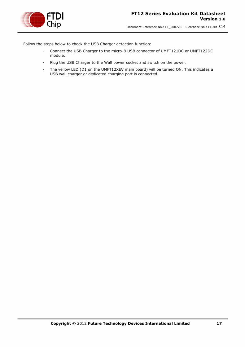
6.4 UMFT122DC Schematic and BOM
Copyright © 2012 Future Technology Devices International Limited 22
FT12 Series Evaluation Kit Datasheet Version 1.0
Document Reference No.: FT_000728 Clearance No.: FTDI# 314
Figure 6-4 UMFT122DC Circuit Schematic
# Designator Comment Description ManufacturerPartNo Manufacturer 1 U1 FT122T Enhanced USB device
controller with parallel interface, TSSOP-28
FT122T FTDI Chip
2 CN1 MicroUSB CONN RCPT STD MICRO USB TYPE B
10104110-0001LF FCI
3 R2, R3 27R/1% Resistor RC0603FR-0727RL Yageo
4 R4 0R Resistor RC0603FR-07000RL Yageo
5 R1 470R Resistor RC0603FR-07470RL Yageo
6 C2 10nf CAP CER 10000PF 50V 10% X7R 0603
C0603C103K5RACTU Kemet
7 FB1 600R/0.5A Chip Ferrite Bead 0805 MPZ1608S601A TDK Corporation
8 C1 4.7uF Polarized Capacitor TAJA475K016RNJ AVX Corporation
9 C3, C4, C5 0.1uF Capacitor bipolar 06035C104KAT2A AVX Corporation
10 D1 Green Typical LED diode APT2012SGC Kingbright Corp
11 J1 Two 1X14 PIN HEADER, 600mil spacing
'Headers & Wire Housings 14P SR UNSHRD HRD .76 GOLD OVER NI
68000-114HLF FCI
Table 6-4 UMFT122DC BOM list

Copyright © 2012 Future Technology Devices International Limited 23
FT12 Series Evaluation Kit Datasheet Version 1.0
Document Reference No.: FT_000728 Clearance No.: FTDI# 314
7 Firmware Upgrade Process
The firmware for the on-board microcontroller LPC1114 can be upgraded through either UART (ISP mode) or JTAG/SWD interface. This section will describe the steps on how to download the firmware through ISP mode. For the usage of JTAG/SWD interface with LPC-Link debug module, please refer to NXP LPCXpresso homepage at http://ics.nxp.com/lpcxpresso/. Note that the LPCXpresso is an integrated development platform for firmware development, debug and download for NXP’s ARM-based LPC
microcontrollers. The LPCXpresso development tool chain can be downloaded from http://lpcxpresso.code-red-tech.com/LPCXpresso/ .
Check the FTDI website for the available pre-compiled firmware for FT12x Evaluation Kit ( http://www.ftdichip.com/Firmware/Precompiled.htm ).
7.1 Put LPC1114 microcontroller in ISP mode
- Use a jumper wire to short pad 38 of J1 to pad 1 or pad 54 of J1. This is to connect the LPC1114 P0_1 pin to GND so that LPC1114 will enter ISP mode after power on or reset.
- Connect the board to the test PC via the micro-USB cable. The USB–A plug shall be inserted in the PC USB port, while the micro-USB-B plug shall be connected to the daughter card USB port. The board will be powered on with the LPC1114 entering ISP mode. Note for self power configuration the daughter card is not required to be present for firmware upgrading. For bus power configuration the daughter card is required as the power comes from the daughter card USB port.
Figure 7-1 Plug in micro USB cable
7.2 Connect the TTL-232R-3V3 cable
- Connect the board to the test PC using a TTL-232R-3V3 cable. Plug the 6-pin socket of the cable
into the CN2 pin header. Please note the direction of the cable, the black wire (GND) should be plugged in to pin 1 of CN2.
- Connect the other end of the TTL-232R-3V3 cable to a USB port of the test PC

Copyright © 2012 Future Technology Devices International Limited 24
FT12 Series Evaluation Kit Datasheet Version 1.0
Document Reference No.: FT_000728 Clearance No.: FTDI# 314
Figure 7-2 Connect TTL-232R-3V3 UART cable
7.3 Upgrade firmware
- Download and install the driver for the FTDI TTL-232R-3V3 cable. Refer to the cable datasheet for details ( http://www.ftdichip.com/Support/Documents/DataSheets/Cables/DS_TTL-232R_CABLES.pdf )
- Download the Flash Magic firmware programming utility from http://www.flashmagictool.com.
- Install the utility on test PC by running “FlashMagic.exe” - Once installation is complete, launch the utility from Start -> All Programs -> Flash Magic ->
Flash Magic. - Configure the tool by the following steps:
o Click “Select Device…”, choose LPC1114/302 from the popup window and click OK o COM port: select the COM port number associated with the TTL-232R-3V3 cable. The
COM port number can be found in the “Device Manager -> Ports (COM & LPT) -> USB
Serial Port (COM3)”. Note on different PC this number can be changed. o Interface: select “FTDI USB-Dongle” from the pull-down list. o Oscillator (MHz): key in ‘12’. o Tick the box “Erase blocks used by Hex File”. o Select Hex File: browse to select the desired firmware binary hex file (ie “LPC1114-
FT12x.hex”).
o Tick the box “Verify after programming” o The tool is configured ready for firmware downloading.
- Click “Start” button and the firmware download will begin. Typically the download takes about 2 minutes. Once completed, a ‘finished’ message will be displayed in the status bar (bottom side),
and the green download progress bar will reach 100%. Note the ‘finished’ message may disappear after a while. If no message is displayed in the status bar after a few minutes, this also indicates that the previous download is completed.
- Power off the board. Remove the ISP jumper wire and then power on the board again. The new firmware will take effect.

Copyright © 2012 Future Technology Devices International Limited 25
FT12 Series Evaluation Kit Datasheet Version 1.0
Document Reference No.: FT_000728 Clearance No.: FTDI# 314
Figure 7-3 Flash Magic configuration
8 Environmental Compliances
The UMFT12XEV main board and UMFT12XDC daughter boards exclusively use lead free components, and are fully compliant with European Union directive 2002/95/EC.

Copyright © 2012 Future Technology Devices International Limited 26
FT12 Series Evaluation Kit Datasheet Version 1.0
Document Reference No.: FT_000728 Clearance No.: FTDI# 314
9 Contact Information
Head Office – Glasgow, UK Future Technology Devices International Limited Unit 1, 2 Seaward Place, Centurion Business Park Glasgow G41 1HH United Kingdom Tel: +44 (0) 141 429 2777 Fax: +44 (0) 141 429 2758 E-mail (Sales) [email protected] E-mail (Support) [email protected] E-mail (General Enquiries) [email protected]
Branch Office – Taipei, Taiwan Future Technology Devices International Limited (Taiwan) 2F, No. 516, Sec. 1, NeiHu Road Taipei 114 Taiwan , R.O.C. Tel: +886 (0) 2 8791 3570 Fax: +886 (0) 2 8791 3576 E-mail (Sales) [email protected] E-mail (Support) [email protected] E-mail (General Enquiries) [email protected]
Branch Office – Hillsboro, Oregon, USA Future Technology Devices International Limited (USA) 7130 SW Fir Loop Tigard, OR 97223 USA Tel: +1 (503) 547 0988 Fax: +1 (503) 547 0987 E-Mail (Sales) [email protected] E-Mail (Support) [email protected] E-Mail (General Enquiries) [email protected]
Branch Office – Shanghai, China Future Technology Devices International Limited (China) Room 1103, No. 666 West Huaihai Road, Shanghai, 200052 China Tel: +86 (0)21 6235 1596 Fax: +86 (0)21 6235 1595 E-mail (Sales) [email protected] E-mail (Support) [email protected] E-mail (General Enquiries) [email protected]
Web Site
http://ftdichip.com
Distributor and Sales Representatives
Please visit the Sales Network page of the FTDI Web site for the contact details of our distributor(s) and sales representative(s) in your country.
System and equipment manufacturers and designers are responsible to ensure that their systems, and any Future Technology Devices International Ltd (FTDI) devices incorporated in their systems, meet all applicable safety, regulatory and system-level performance requirements. All application-related information in this document (including application descriptions, suggested FTDI devices and other materials) is provided for reference only. While FTDI has taken care to assure it is accurate, this information is subject to customer confirmation, and FTDI disclaims all liability for system designs and for any applications assistance provided by FTDI. Use of FTDI devices in life support and/or safety applications is entirely at the user’s risk, and the user agrees to defend, indemnify and hold harmless FTDI from any and all damages, claims, suits or expense resulting from such use. This document is subject to change without notice. No freedom to use patents or other intellectual property rights is implied by the publication of this document. Neither the whole nor any part of the information contained in, or the product described in this document, may be adapted or reproduced in any material or electronic form without the prior written consent of the copyright holder. Future Technology Devices International Ltd, Unit 1, 2 Seaward Place, Centurion Business Park, Glasgow G41 1HH, United Kingdom. Scotland Registered Company Number: SC136640
Copyright © 2012 Future Technology Devices International Limited 27
FT12 Series Evaluation Kit Datasheet Version 1.0
Document Reference No.: FT_000728 Clearance No.: FTDI# 314
Appendix A - List of Figures and Tables
List of Figures
Figure 3-1 UMFT12XEV main board ............................................................................................................... 4
Figure 3-2 UMFT120DC daughter board ........................................................................................................ 4
Figure 3-3 UMFT121DC daughter board ........................................................................................................ 6
Figure 3-4 UMFT122DC daughter board ........................................................................................................ 7
Figure 3-5 Micro-B to Standard-A cable ........................................................................................................ 8
Figure 3-6 TTL-232R-3V3 USB cable .............................................................................................................. 8
Figure 3-7 LPC-Link debugger module ......................................................................................................... 9
Figure 4-1 Plug the daughter board module to the main board................................................................ 10
Figure 4-2 JP2 default setting ...................................................................................................................... 11
Figure 4-3 JP3 and JP4 default setting........................................................................................................ 11
Figure 4-4 Device manager window ............................................................................................................. 12
Figure 4-5 Drive property window ................................................................................................................ 12
Figure 4-6 Update driver window ................................................................................................................. 13
Figure 4-7 Update driver window ................................................................................................................. 13
Figure 4-8 Update driver window ................................................................................................................. 14
Figure 4-9 Update driver window ................................................................................................................. 14
Figure 4-10 Install from disk window ........................................................................................................... 15
Figure 5-1 Serial Loopback Test .................................................................................................................. 16
Figure 6-1 UMFT12XEV Circuit Schematic .................................................................................................. 18
Figure 6-2 UMFT120DC Circuit Schematic .................................................................................................. 20
Figure 6-3 UMFT121DC Circuit Schematic .................................................................................................. 21
Figure 6-4 UMFT122DC Circuit Schematic .................................................................................................. 22
Figure 7-1 Plug in micro USB cable ............................................................................................................. 24
Figure 7-2 Connect TTL-232R-3V3 UART cable .......................................................................................... 24
Figure 7-3 Flash Magic configuration .......................................................................................................... 25
List of Tables
Table 2-1 Ordering information ...................................................................................................................... 1
Table 3-1 UMFT120DC J1 Pin Out Description ............................................................................................. 5
Table 3-2 UMFT121DC J1 Pin Out Description ............................................................................................. 6
Table 3-3 UMFT122DC J1 Pin Out Description ............................................................................................. 8
Table 4-1 Default setting of the jumpers ..................................................................................................... 10
Table 6-1 UMFT12XEV BOM list ................................................................................................................... 19
Table 6-2 UMFT120DC BOM list ................................................................................................................... 20

Copyright © 2012 Future Technology Devices International Limited 28
FT12 Series Evaluation Kit Datasheet Version 1.0
Document Reference No.: FT_000728 Clearance No.: FTDI# 314
Table 6-3 UMFT121DC BOM list ................................................................................................................... 21
Table 6-4 UMFT122DC BOM list ................................................................................................................... 22
Table A-1 Abbreviations................................................................................................................................ 29
Table A-2 References .................................................................................................................................... 29

Copyright © 2012 Future Technology Devices International Limited 29
FT12 Series Evaluation Kit Datasheet Version 1.0
Document Reference No.: FT_000728 Clearance No.: FTDI# 314
Appendix B – Abbreviations and References
Term Description
CDC Communications Device Class
DUT Device Under Test
GPIO General Purpose Input/Output
HID Human Interface Device
ISP In System Program
JTAG Joint Test Action Group
LED Light Emitting Diode
MCU Micro Controller Unit
OS Operating System
PCB Printed Circuit Board
SPI Serial Parallel Interface
SWD Serial Wire Debug
UART Universal Asynchronous Receiver/Transmitter
USB Universal Serial Bus
VCP Virtual COM Port
Table A-1 Abbreviations
Title Description
FT_000646 FT120 IC data sheet
FT_000648 FT121 IC data sheet
FT_000647 FT122 IC data sheet
AN_209 PDIUSBD12 to FT120 Migration Guide
AN_225 FT12x firmware programming guide
TTL-232R-3V3 USB cable
USB to UART converter cable. Refer to http://www.ftdichip.com/Products/Cables/USBTTLSerial.htm
Serial Loopback
test utility
http://www.madsencircuits.com/serial_loopback.html
Flash Magic LPC microcontroller firmware programming tool. Refer to http://www.flashmagictool.com
LPCXpresso LPC microcontroller integrated development platform. Refer to
http://ics.nxp.com/lpcxpresso/ and http://lpcxpresso.code-red-tech.com/LPCXpresso/
Table A-2 References

Copyright © 2012 Future Technology Devices International Limited 30
FT12 Series Evaluation Kit Datasheet Version 1.0
Document Reference No.: FT_000728 Clearance No.: FTDI# 314
Appendix C - Revision History
Document Title: DS_UMFT12xA FT12 Series Evaluation Kit datasheet
Document Reference No.: FT_000728
Clearance No.: FTDI#314
Product Page: http://www.ftdichip.com/Products/Modules/DevelopmentModules.htm
Document Feedback: Send Feedback
Version 1.0 1.0 Created 03/09/2012