Embed Size (px)
Citation preview

Fully Integrated Silicon Terahertz Transceivers for
Sensing and Communication Applications
Jung-Dong Park
Electrical Engineering and Computer SciencesUniversity of California at Berkeley
Technical Report No. UCB/EECS-2013-36
http://www.eecs.berkeley.edu/Pubs/TechRpts/2013/EECS-2013-36.html
May 1, 2013

Copyright © 2013, by the author(s).All rights reserved.
Permission to make digital or hard copies of all or part of this work forpersonal or classroom use is granted without fee provided that copies arenot made or distributed for profit or commercial advantage and that copiesbear this notice and the full citation on the first page. To copy otherwise, torepublish, to post on servers or to redistribute to lists, requires prior specificpermission.

Fully Integrated Silicon Terahertz Transceivers for Sensing and Communication Applications
By
Jung-Dong Park
A dissertation submitted in partial satisfaction of the
requirements for the degree of
Doctor of Philosophy
in
Engineering - Electrical Engineering and Computer Sciences
in the
Graduate Division
of the
University of California, Berkeley
Committee in charge:
Professor Ali M. Niknejad, Chair
Professor Jan M. Rabaey
Professor Paul K. Wright
Spring 2012

Fully Integrated Silicon Terahertz Transceivers for Sensing and Communication Applications
Copyright © 2012
by
Jung-Dong Park

1
Abstract
Fully Integrated Silicon Terahertz Transceivers for Sensing and Communication Applications
by
Jung-Dong Park
Doctor of Philosophy in Engineering – Electrical Engineering and Computer Sciences
University of California, Berkeley
Professor Ali M. Niknejad, Chair
With advancement of the silicon device, we have witnessed revolutionary achievements in RF and millimeter-wave integrated circuit (IC) technology during last decade. Reflecting the impact of the RFICs in its compactness, low-cost, and mass production, the Terahertz Silicon Integrated Circuit (THz-IC) will open a new era in imaging, sensing, spectroscopy, and ultrafast wireless communication. This thesis mainly explores two fully integrated terahertz transceivers for sensing and communication applications in well matured 0.13 µm BiCMOS and 65 nm digital CMOS technology. Since antenna size shrinks quadratically as radiation frequency increases for a given gain, on-chip antennas have great potential in terahertz range by eliminating packaging issues for cost-effective, compact terahertz transceivers. To achieve high radiation efficiency, we investigate the loss mechanisms of several on-chip antennas implemented in conventional (Bi) CMOS technologies. By introducing a compact N-push clamping harmonic generator utilizing the transformer-coupled push-push structure with Coplanar Stripline (CPS), the fundamental signal filtering is effectively achieved by highly rejecting the common-mode input. The designed N-push harmonic generator with proposed architecture is robust to the phase mismatch in driving signals. A 0.38 THz Frequency Modulated Continuous Wave (FMCW) radar transceiver is presented with the ranging and detection of a target in 10 cm. A 0.26 THz fully integrated CMOS transceiver is demonstrated for wireless chip to chip communication. The non-coherent On-Off Keying (OOK) transceiver with dual antenna chains is implemented to overcome the limited device performance in 65 nm CMOS which achieves +5 dBm of the Equivalent Isotropically Radiated Power (EIRP).

i
To my wife for her devoted love,
to my son and daughters for their endless love,
and to my parents for their unbounded love and support.

ii
Contents
List of Figures iv
List of Tables vii
1 Introduction 1
1.1 Terahertz Overview………………………………………………………………………...2
1.1.1 Terahertz Regime………….…………………………………………….……………2
1.1.2 Terahertz Gap.…………………………………………………………...……………2
1.1.3 Terahertz Source in Photonics……….………….……………….……………………3
1.1.4 Terahertz Source in Electronics…………………….………………...………………4
1.2 Terahertz Applications….…………………………………………………………...……10
1.2.1 Terahertz Sensing……..………………………………………………………..……10
1.2.2 Terahertz Short Range Communication…………………………………..…………11
1.3 Atmospheric Attenuation in Terahertz………………………………………...………….12
1.4 Thesis Outline……………………………………………………………………….…....13
2 On-chip Antennas in (Bi) CMOS Technology 14
2.1 Introduction………………………………….……………………………………………14
2.2 Loss Mechanism in On-chip Antenna in Silicon.…...……………………………………15
2.2.1 Loss from Low Resistive Silicon Substrate…...….………….……………………...15
2.2.2 Surface-wave Mode Excitation on Silicon Substrate………………………..……....16
2.3 Wafer-thinning Approach for Dipole and Slot Antennas...………………………………18
2.3.1 Antenna Radiation Efficiency……………………….………………………………18
2.3.2 On-chip Folded Slot Antenna with Thinned Silicon Substrate...…………………....19
2.3.3 100 GHz Folded Slot Antenna Design with Wafer-thinning…………..……………20
2.4 On-chip Antenna with Microstrip Structure……………………………………...………22
2.4.1 Microstrip Rectangular Patch Antenna………...….……………….…..……………22
2.4.2 Microstrip Half-width Leaky-wave Antenna…..……………………………………31
2.5 Conclusion……...…...……...………………………………………………….…………37
3 A 0.38 THz Fully Integrated FMCW Radar Transceiver in BiCMOS 38
3.1 Introduction……………………………...……………………………………….…….…38
3.2 Harmonic Generation with N-Push Circuitry……………………......................................39
3.2.1 Generalized N-push Harmonic generator……...……………………………….……39
3.2.2 BJT Clamping Circuit Analysis..…...…………………………………………….…40
3.3 Terahertz FMCW Transceiver Design…...……………………………………………….48
3.3.1 Terahertz FMCW Transceiver Architecture……...……….…………………...……48

iii
3.3.2 Fundamental Signal Generation………………………………..……………………50
3.3.3 Transmitter Circuit Design…………………………………………..………………53
3.3.4 Receiver Circuit Design………………………………………..……...…….………56
3.4 Passive Elements……………………………………………………………………….....59
3.4.1 Coplanar Stripline (CPS) Characterization………..…………………...……………59
3.4.2 On-chip Patch Antenna Design…………………………………….…..……………63
3.5 Measurement………………………………………………………………...……………65
3.6 Conclusion……………………………………………..…………………...…………….68
4 A 0.26 THz Fully Integrated Wireless Transceiver in CMOS 73
4.1 Introduction………………………………………………………………...……………..73
4.2 Short Range Communication System……………………………………...…………......74
4.2.1 Required Signal to Noise Ratio………………………………………..…….……....74
4.2.2 Multiple Antenna Transceiver with Spatial Diversity……..…………...……………75
4.2.3 Modulation Scheme for Terahertz Short Range Communication……...……............77
4.2.4 Link Budget Analysis…………………………………………..……………………80
4.3 CMOS Terahertz Wireless Transceiver Architecture………………………...…..………82
4.4 Transmitter Circuits…………………………………………………………...………….84
4.4.1 260 GHz Quadrupler……………………………………………………..……….....84
4.4.2 V-band Hybrid…………………………………………………………………….....86
4.4.3 Distributed Non-coherent OOK Modulator in V-band…………………...………....88
4.4.4 V-band D-1 Power Amplifier….….……………………………………...…………..90
4.4.5 PRBS Generator.. ………………………………………………………...…….……93
4.5 Receiver Circuits…………………………………………………..…………...…………94
4.5.1 195 GHz Tripler………………………………………….………………………….94
4.5.2 Demodulator……………………………………………….……………...…….…...97
4.5.3 260 GHz Double Balanced Mixer……….………………….……………....……….99
4.5.4 V-band Wideband IF Amplifier……………………….…….……………...….…..101
4.5.5 V-band Voltage Controlled Oscillator………………….….………….…...………103
4.6 Tx/Rx Dual On-chip Antenna Design ………………………….……………………….104
4.6.1 Half-width Microstrip Leaky-wave Antenna……………….……..……………….104
4.6.2 Tx/Rx Dual Half-width MLWA….…………...…………………………...……….104
4.7 Measurement…………………………………………………………………………….107
4.8 Conclusion………………………………………………………………………………110
5 Conclusion 111
5.1 Thesis Summary…………………………………………………………………………111
5.2 Future Directions………………………………………………………………………112
Bibliography 114

iv
List of Figures
1.1 Unique terahertz region placed in the transition region………...……………………………..2
1.2. Reported THz-emission power output as a function of frequency…………………………...3
1.3. Current gain cut-off frequency (fT) of NMOS, SiGe HBT, and InP HEMT…………...........6
1.4. Maximum oscillation frequency (fmax) of NMOS, SiGe HBT, and InP HEMT……………6
1.5. SEM microphotographs of the device cross-section……………………………………...7
1.6. Flow chart of the terahertz circuit design in CAD case……………………………………..9
1.7. Application examples of terahertz sensing………………………………………………….10
1.8. Application examples of terahertz communication…………………………………………11
1.9. Specific attenuation of the earth’s atmosphere……….……………………………………..12
2.1. The two main loss mechanisms of the on-chip antenna ……………………………………15
2.2. Reported on-chip antennas by reducing resistive loss………………………………………16
2.3. Critical substrate thickness (hc) as a function of frequency permittivity……………………17
2.4. Reported on-chip antennas by suppressing surface-wave excitation mode……………….18
2.5. Structural dimension of the designed folded slot antenna with a meandered stub…………20
2.6. Input impedance of the designed folded slot with a meandered stub……………………….21
2.7. Simulated radiation patterns of the folded slot antenna……………………………………..22
2.8. Geometry of the edge-fed microstrip rectangular patch antenna with inset……………….23
2.9. Calculated radiation efficiency of the rectangular patch antenna……..…………………….28
2.10. Calculated 1/Q factor of the rectangular patch antenna……………………………………28
2.11. Calculated fractional bandwidth of the rectangular patch antenna……………………….29
2.12. Calculated antenna directivity and gain of the rectangular patch antenna……………….29
2.13. Simulated radiation pattern of the designed microstrip edge-fed patch antenna…………30
2.14. Simulated return loss of the single rectangular patch antenna in 50 Ω input impedance….31
2.15. Geometry of the half-width microstrip leaky-wave antenna (MLWA)………………..34
2.16. Equivalent circuit for transmission resonance method (TRM)…………………………….34
2.17. Calculated phase and attenuation constant as a function of the radiation frequency………36
2.18. Simulated radiation pattern of the single half-width MLWA vs. frequency………………37
3.1. Schematic diagram of the N-push harmonic generator..……………………………………39
3.2. Simplified equivalent BJT clamping circuit for an analytical expression…………………41
3.3. Clamped cosinusoidal model for a hard switching BJT ………………………………….41
3.4. Coefficient of expansion (γk(θ)) of the clamped cosinusoidal output current..…………….43
3.5. Comparison of transit emitter current between SPICE and proposed model........................46
3.6. Comparison of harmonic components between SPICE and proposed model………………46
3.7. Principle the homodyne FMCW radar…...………………...……...………………………...49

v
3.8. Block diagram of the designed homodyne FMCW transceiver……………………………49
3.9. Schematic diagram of the THz transceiver………………………………………………….50
3.10. Circuit diagram of (a) Colpitts VCO and (b) driving amplifier...…………………………51
3.11. Simulated S-parameters of the designed single to differential driving amplifier………….51
3.12. Simulated output power for the designed single to differential driving amplifier…………52
3.13. Simulated phase and amplitude mismatch of the designed size reduced hybrid…………52
3.14. Circuit diagram of the Tx quadrupler ……………………………………………………..53
3.15. Comparison of the Tx antenna input impedance w/ and w/o ground center tap.……..……54
3.16. Output waveforms of the quadrupler with (a) designed antenna (b) ideal load……………54
3.17. Output harmonics of the transmitter as a function of I/Q phase mismatch………………55
3.18. Circuit diagram of the 2nd harmonic quadrature LO generator….…………………………56
3.19. Output harmonics of the 2nd harmonic LO generator for I/Q phase mismatch…………….57
3.20. Circuit diagram of the Rx subharmonic double-balanced mixer…………………………..58
3.21. Power conversion loss and NF of the receiver as a function of 2f0 LO input power………58
3.22. Structure of the Coplanar Stripline (CPS)….……………………………………………...59
3.23. Definition of mixed mode Scattering parameters………………………………………….60
3.24. (a) Port assignment for S-parameter extraction (b) Equivalent model for CPS...................61 3.25. Differential-mode Z0 contour of the CPS depending on the width and gap……………....62
3.26. Differential-mode α (dB/mm) contour of the CPS depending on the width and gap……...62
3.27. (a) The structure of the Tx on-chip patch antenna and (b) The radiation pattern…………64
3.28. (a) The structure of the Rx on-chip patch antenna and (b) The radiation pattern………….65
3.29. Microphotograph of the fabricated 0.38 THz FMCW radar transceiver ……..……….66
3.30. Measured phase noise of the stand alone VCO……………………………………………66
3.31. Measurement setup for VCO characterization of the in-situ VCO………………………67
3.32. Measurement setup for the EIRP of the transmitter………………………………………..69
3.33. Comparison between measured EIRP and simulated output power vs. the base bias……..69
3.34. Measured EIRP with calorimeter as a function of the VCO control voltage………………70
3.35 Measured IF output spectrum w/ a target positioned 5 cm distance from TRx……….70
3.36. Measured IF output spectrum with maximum frequency chirp in VCO…………………71
3.37. Measured IF output spectrum w/ and w/o a target 10 cm distance from TRx…………......71
3.38. Measured IF output when the target is misaligned…………...……………………………72
4.1. Terahertz short range communication for wireless chip to chip interconnection ...………...74
4.2. Multiple antenna (a) transmitter (b) receiver for the terahertz wireless link……….……….76
4.3. Schematic diagram of OOK modulation scheme, and its constellation diagram…………79
4.4. Schematic diagram of QPSK modulation scheme, and its constellation diagram…………..80
4.5. Required number of array for a TRx with QPSK modulation scheme……………………...81
4.6. Required number of array for a TRx with coherent OOK modulation scheme………...…...81
4.7. Required number of array for a TRx with non-coherent OOK modulation scheme……..…82

vi
4.8. Block diagram of designed THz wireless transceiver……………………………………..83
4.9. Circuit diagram of the Tx quadrupler with the quadruple-push harmonic structure..……..85
4.10. Output harmonics of the Tx quadrupler as a function of I/Q phase mismatch………….…85
4.11. Simulated quadrupler Pout of harmonic components vs. total Pin……………………….86
4.12. Structure of the meandered hybrid with capacitive load CT……….…………………..…..87
4.13. Simulated S-parameters in dB for the designed size reduced hybrid……………………...87
4.14. Simulated phases of S21 and S31 for the designed size reduced hybrid…………………….88
4.15. Circuit diagram of the Transmitter distributed non-coherent OOK modulator...………….89
4.16. Simulated isolation and thru in dB for the distributed non-coherent OOK modulator.….89
4.17. Simulated non-coherent OOK modulated output signal of the power amplifier……...…90
4.18. Schematic diagram of Class D-1 power amplifier…….……………………………………91
4.19. Drain efficiency as a function of tank capacitance ratio and switch scaling factor………92
4.20. Output power as a function of tank capacitance ratio and switch scaling factor…………..92
4.21. Schematic diagram of the PRBS generator with interleaved architecture…………………93
4.22 Circuit diagrams of the CML components used in the PRBS generator…………………94
4.23. Circuit diagram of the receiver LO tripler with balanced hair pin filters………………….95
4.24. Simulated differential S21 and S11 in dB for the balanced hairpin filter…………………....96
4.25. Simulated tripler Pout of harmonic components depending on the input Pin……………….96
4.26. Circuit diagram of the receiver demodulator with two push-push structures…………….97
4.27. Output voltage of the demodulated signals as a function of the total input power………...98
4.28. Demodulated output voltage waveform with 20 Gb/s OOK modulated input signal……98
4.29. Circuit diagram of the down converting mixer with two push-push structures………….100
4.30. Simulated conversion gain and noise figure as a function of LO driving power………100
4.31. Schematic diagram of the wideband IF amplifier………………………………….……..102
4.32. Simulated output with N-OOK modulated 60 GHz signal with 10 Gb/s data rate……….102
4.33. Circuit diagram of the VCO with a cascade buffer……………………………………….103
4.34. Measured Sweep frequency of Tx and Rx VCO as a function of the control voltage……103
4.35. Structure of the four-elements arrayed Tx/Rx dual leaky-wave antenna…………...……105
4.36. Simulated radiation pattern (Gain) of the designed half-width MLWA vs. frequency….105
4.37. Simulated return loss of the designed half-width MLWA vs. frequency………………...106
4.38. Microphotograph of the 0.26 THz CMOS wireless transceiver…………………………106
4.39. Measurement setup for the EIRP of the transmitter…………………………………….107
4.40. Measured radiation pattern in H-plane at 0.246 THz…………………………………..108
4.41. Measurement setup for the spectrum of the transmitter at fundamental frequency………108
4.42. Measured spectral spacing for the fundamental signal with 14 Gb/s of modulation……..109
4.43. Test setup for the short range wireless communication link……………………………...109
4.44. The measured spectrum of the 6 Gb/s demodulated toggling signal ……………………110

vii
List of Tables
2.1. Reported on-chip antennas in silicon substrate…………………………………………….19
viii
Acknowledgements
This work would not have been possible without the help and influence of many wonderful and talented people. I would first like to express my sincerest gratitude to my advisor Prof. Ali M. Niknejad for his countless help and support. He has always been generous, attentive, available and supportive throughout all the peaks and valleys of my Ph.D. journey. My work in Berkeley has been constructed mainly inspired by his shining perspective, tireless enthusiasm, amazing engineering-intuition, and firm and solid knowledge. I would like to express my sincere thanks to Prof. Jan M. Rabaey and Prof. Paul K. Wright for serving on both my qualifying examination committee and my dissertation committee. I also thank to Prof. Ahmad Bahai for being a part of my qualifying examination committee. I am grateful for all the support and advice of Prof. Elad Alon throughout my research works during Ph.D. course.
My collaboration with Shinwon Kang and Siva V Thyagarajan in designing transceivers was particularly fruitful and enjoyable. Without their contribution, my journey might be more tough and lonely. Especially I am grateful for valuable technical discussions among us. I also give special thanks to Dr. Dick Plambeck for his encouragement and generous support of the terahertz instruments. I thank to seniors at BWRC who have provided so much insight and technical advice: Zhiming Deng, Amin Arbabian, Debopriyo Chowdhury, and Cristian Marcu, and thank to visiting researchers: Jay Wang, Dr. Vason Srini, Stefano Dal Toso, and Gyungtae Moon. I would like to give many thanks to my peer students: Lu Ye, Jiashu Chen, Jun-Chau Chien, Ashkan Borna, Mariam Tabesh, Lingkai Kong, Chintan Thakkar, Yue Lu, Ping-Chen Hwang, Paul Liu, Yida Duan, Han-Phuc Lee, and many BWRC colleagues for their help and technical discussion. I would like to express sincere thanks to Mrs. Ruth Gjerde in Cory Hall for her kindness, and encouragement to me. I am grateful to BWRC staff: Tom, Kevin, Brian, Bira, and Olivia for their kindness and consistency in assisting students.
Many Korean students helped me to keep going forward. I would like to give a special thanks to all the Korean circuit nerds: Ji-Hoon Park, Kyuhyun Noh, Namseog Kim, Kwangmo Jung, and Jaehwa Kwak. The Korean seniors Changhwan Shin, Kanghoon Jeon, Jemin Park gave me invaluable information and encouragement for me to adapt a new life in Berkeley. Many thanks to Min Hee Cho, Se Young Park, Jaeseok Jeon, Seonghwan Kim, Young-Ki Yoon, and Prof. Hyuck Choo for their help. I also give special thanks to Byeong-Gyu Nam and Dan An.
My journey became possible by encouragement, support, and recommendation of Prof. Jin-Koo Rhee who introduced me electronics, Prof. Jong-In Song who taught me research skills and attitudes, Prof. Hyun-Chang Park, Prof. Sam-Dong Kim, Prof. Chee Sun Won, Dr. Wan-Joo Kim, and the Late Prof. Un-Chul Paek who has been a role model as a great researcher and educator in his whole life.
Finally, I would like to express deepest gratitude to my parents for their love and endless support. Without their devotion and sacrifice, I could not be where I am today. I also express my sincere gratitude to my mother-in-law. I would like to special thanks to my truthful siblings, Young-Sun, Bong-Jin, and Ju-Ha for always being there for me. My academic journey must be something like walking though the dessert without my lovely sweeties: Juhyun who has always tried to find four leaf clovers in the village courtyard hoping for my graduation, Hyunjoong who has always shown happiest smile to me, and Seohyun who made our family live together here in Berkeley. Most special thanks have to go to my loving wife, Sunsook Moon who has sacrificed and devoted everything that she had for my academic journey in Berkeley.

1
Chapter 1
Introduction
Terahertz (THz) technology has gained high interests in various applications owing to its unique characteristics. Generally, the terahertz range is widely conceived as 0.3 THz to 3 THz whose wavelength (λ) is between 1 mm to 0.1 mm, a transition region between electronics and photonics [Siegel02]. It has great potential in sensing and communication applications. Terahertz radiation can penetrate dielectric materials without causing any destructive ionization of the material. In the category of sensing applications, the terahertz imager can achieve much higher imaging resolution than millimeter-wave counterpart. Terahertz radiation has been widely used in spectroscopy by using the vibration of molecules for a given terahertz radiation frequency which can produce a unique fingerprint depending on type of dielectric materials. Biomedical spectroscopy [Wallace04] [Pickwell06] [Ajito09], and remote gas sensing [Oh09] are the promising examples of the application. Owing to extremely short wavelength, the terahertz compact range is useful for indoor millimeter-wave radar cross section (RCS) characterization of tanks and aircrafts [Danylov10]. The terahertz spectrum has great potential in ultrafast wireless communication by providing wide bandwidth in the new spectrum regime [Piesiewicz07] [Federici10]. In order to expand the use of the electromagnetic spectrum as such, designing highly efficient compact sources and detectors are essential. However there exist many challenges in achieving compact, reliable sources and detectors in this transition spectrum regime. Enormous research efforts have been directed to bridge this gap with different approaches from high-frequency electronics and photonics [Siegel02] [Tonouchi07] [Williams07].
Until recently fully integrated THz transceiver in silicon has not been considered a promising solution due to the limited device performance and the large propagation losses coupled through a resistive silicon substrate in terahertz range. However, we have witnessed revolutionary achievements in RF and millimeter-wave integrated circuit (IC) technology during last decade with advancement of the nano-scale silicon technology. Considering the impact of the RFICs in its compactness, low-cost, and mass production, the “THz-IC” will open a new era in imaging, sensing, spectroscopy, and ultrafast wireless communication. This thesis explores the realization of the fully integrated terahertz transceivers for sensing and communication applications in BiCMOS and digital CMOS technologies.

2
1.1 Terahertz Overview
1.1.1 Terahertz Regime
The terahertz range generally implies the unique frequency range which lies between the microwaves and infrared in the electromagnetic spectrum as presented in Fig. 1.1. Owing to this loosely defined range, slightly different frequency ranges are considered as terahertz regime in the literatures. Roughly, it ranges between 0.1 THz to 30 THz [Tonouchi07]. In some literatures of photonics society, it is conceived as 0.3 THz to 10 THz [Williams07] while microwave electronics society typically considers the terahertz range as 0.3 THz to 3 THz [Siegel02] which is synonymously termed submillimeter-wave range. In this thesis we mainly explore the lower frequency range of terahertz regime around 0.3 THz.
1.1.2 Terahertz Gap
Placed in a unique position in the electromagnetic spectrum― a transition region between the realm of microwave electronics and photonics, terahertz-wave has unique characteristics in sensing and communication applications. However the technology has not been matured as much as microwave or optical technology. The terahertz radiation is limited to milliwatt range around 2 THz in photonics approach and it is around 0.1 milliwatt range around 0.5 THz in high-frequency electronics approach. While the wavelength of terahertz source limits a high photon energy generation (E=hν) from the photonics, the performance of the electronic THz source and detector is severely limited by active device performance from the approach of high-frequency electronics. Moreover, the measurement instrumentation at terahertz regime is scarce and expensive. When we approach the realization of terahertz source in electronics, the output power is limited by the active device performance ( fT / fmax ). Owing to this reason, current status of THz technology for generating, detecting, and analyzing terahertz radiation is not as advanced as high-frequency electronics or infrared photonics. This technological barrier is generally conceived as the ‘Terahertz gap’ [Sigel02] [Huang08]. Fig. 1.2 shows the output power of the reported signal sources depending on operating frequency which clearly shows the lack of sources in submillimeter-wave range [Tonouchi07].
Figure 1.1. Unique terahertz region placed in a transition region between microwaves and infrared in the electromagnetic spectrum.
MF HF VHF UHF SHF EHF X-rayvisible
100 103
Kilo106
Mega109
Giga1012
Tera1015
Peta1018
Eta1021
Zetta
Electronics Photonics0.3 THz ~ 3 THz
γ-ray

3
Figure 1.2. Reported THz-emission power output as a function of frequency: the terahertz-gap, the lack of strong and reliable THz sources, is evident in submillimeter-wave range [Tonouchi07] © Nature Photonics.
1.1.3 Terahertz Source in Photonics
Many research efforts have been directed to close this terahertz gap in photonics. Quantum cascade laser (QCL) has been considered one of the promising solid-state terahertz source with average optical power levels of much greater than a milliwatt since it was first developed in 1994 [Faist94]. Researchers have demonstrated THz-QCL below 2 THz. Monolithic integration of a terahertz QCL and diode mixer has been also demonstrated to form a terahertz photonic integrated circuit [Wanke10]. However, THz-QCLs are required to be cryogenically cooled whose operating temperature is proportional to operating frequency ω.
Bk
kTω=max (°K) (1.1)
where the proportionality constant k =1~1.9 for low frequency QCLs, and 2 mW of output power at 1.8 THz was achieved in Tmax=155 °K [Kumar11]. From (1.1), the operating temperature of QCL at 1 THz scales only to 86 °K.
Uni-traveling carrier photodiode (UTC-PD) with low wavelength laser diode (LD) is another popular approach to generate terahertz signal around 0.3 THz. High quality terahertz waves can be generated by the photo-mixing of two different wavelength laser diodes which produces the optical beat frequency of the two LDs. The beat frequency is typically tunable upto 1.5 THz [Tounouchi07], and the reported output power of the UTC-PD module in 0.35 THz is around 0.5 mW [Wakatsuki08]. Using high-gain lens antennas, discrete PD, LD, and UTC-PD, a 0.3 THz wireless transceiver module has been reported with 12.5 Gb/s in ASK modulation scheme over 0.5 m link range [Song10].

4
1.1.4 Terahertz Source in Electronics
In microwave and solid-state circuit technology, there are many ways available to generate lower frequency range of the terahertz sources. With advancement of extremely high speed III-V compound semiconductor, a fundamental frequency oscillator is feasible in the lower terahertz range. Owing to the limited device performance of silicon devices, harmonics generated from nonlinear characteristics are used widely in (Bi) CMOS technology. Fundamentally the harmonic output power is limited to 1/k2 for kth harmonic component from a nonlinear resistive device [Page56]. Hence most of the harmonic oscillators and multiplier chains driven by mm-wave oscillator severely suffer from the lack of output power. To generate higher output power, the order of desired harmonic should be minimized which naturally requires high performance device.
1.1.4.1 Active Device Performance
For an electronic active device, the high-frequency performance is evaluated with two important figures of merit (FOMs), one is the current gain cut-off frequency (fT), and the other is the maximum oscillation frequency (fmax) which is the highest frequency that an active device is capable of providing power gain. Therefore fmax represents a critical limitation of amplifier and fundamental-frequency oscillator designs for a given device.
As technology node scales down, the gate length of FET and base width of BJT shrink and these two FOMs improve. While fT is mainly determined by intrinsic parameters of the device, fmax is a strong function of device layout as well as device fT. Hence a careful layout is important to minimize external parasitics associated with routings and interconnections to achieve higher device fmax. The ratio fmax/fT can be used to evaluate optimality of the layout [Heydari08]. The device FOMs, fT and fmax for FET are given by [Gray04] [Lee05]
,22
3
)(2 2 ovg
n
gdgs
mFETT V
LCC
gf
πμ
π≈
+= or a
gL
1∝ (1.2)
))((2max
gdmgdgsdsg
gdgsFET
TFET
CgCCgr
CCff
+++
≈ (1.3)
The quantitative expressions for fT and fmax of BJT are similar to those of FET as follows [Herkx97]
,)(2
1
2
12 T
B
nm
Fje
mBJTT V
WCC
g
CC
gf
πμ
πτπ μπμ
≈+
=
+
+= or b
BW
1∝ (1.4)
μπ Cr
ff
b
BJTTBJT
8max ≈ (1.5)
where a, and b denote scaling factors of gate length and emitter width, respectively.

5
With crude estimations using the quadratic equation of FET and the diffusion equation of HBT for Fτ , we see the fT improves quadratically with device scale-down. In advanced silicon technology, the performance improves almost linearly with the scale-down due to secondary effects like carrier velocity saturation. From (1.3) and (1.5), the Miller parasitics between gate-drain or base-collector (Cgd, Cµ) and the loss at gate or base (rg, rb) mainly affect on the available power gain as well as noise factor of the device.
While fmax is the FOM for the power gain of an amplifier and fundamental oscillation, fT is directly related to the minimum noise factor Fmin given by [Fukui79]
)(1min sgmT
f rrgf
fkF ++≈ (1.6)
where fk is Fukui’s empirical noise factor coefficient which is close to 2 [Fukui79], and can be
physically described as gmfk γ2= with γgm is the gm referenced excess noise factor [Cui07]. As
technology node move forward, Fmin improves with increased gm from the scaling-down of gate length (Lg) and oxide thickness (tox), but it is negatively impacted by increased parasitic components (i.e. Cgs, rg) from the higher fringe capacitances and resistances due to the tighter pitch size.
The FOMs, fT and fmax of a device are estimated by measuring 2-port S-parameters of common source (emitter) device using the vector network analyzer. The magnitude of current gain |h21| is extracted given by
21122211
2121 )1)(1(
2
SSSS
Sh
++−−= (1.7)
Fig. 1.3 and Fig. 1.4 present fT and fmax of NMOS, SiGe HBT, and InP HEMT devices in the 2011 International Technology Roadmap for Semiconductors (ITRS) [ITRS2011]. Here fT and fmax were determined by peak fT measured from |h21|, and unilateral gain U extrapolated from 40 GHz with a 20 dB/dec slope, respectively. The scaling factor a of NMOS is close to 1.5, and b of SiGe BJT is about 1 from the trend reported in the roadmap as shown in the figure.
In terms of manufacturability, the required fT and fmax of the CMOS technology of the roadmap look quite challenging. In the 2011 ITRS report, CMOS with 24 nm of the gate-length (Lg) has been reported to have optimized manufacturable solutions yet. Up until 18 nm CMOS, manufacturable solutions are known which has fT =512 GHz, and fmax =439 GHz.
Another challenge in using CMOS in extremely high-frequency applications is that the intrinsic gain gm/gds of the CMOS decreases with scale-down. From the 250 nm to the 45 nm node, the intrinsic voltage gain gm/gds has decreased from 15 to 5 due to an increased gds. If this trend continues, extrapolation for 10 nm technology leads to an intrinsic gain close to unity. In this case, it would not be possible to design any useful RF amplifier. Another difficulty arises from a fabrication of thin oxide layer. In order to obtain channel control over the gate, an oxide thickness tox of around 1 nm is required for the 10 nm node. Further reduction of tox less than 1 nm is difficult considering gate leakage, flicker noise, and process variation. As process node moves forward, total height of the inter-metal dielectric (IMD) layers also scales down which increases the influence of the substrate losses on the propagation for thinner IMD layers. Hence the attenuation the transmission-line increases and the radiation efficiency of the on-chip antennas are severely degraded which is briefly discussed in Chapter 2.

6
Figure 1.3. Current gain cut-off frequency (fT) of NMOS, SiGe HBT, and InP HEMT in ITRS 2011 [ITRS2011].
Figure 1.4. Maximum oscillation frequency (fmax) of NMOS, SiGe HBT, and InP HEMT in ITRS 2011 [ITRS2011].
2010 2011 2012 2013 2014 2015 2016 2017 2018 2019
200
300
400
500
600
700
800 InP HEMT SiGe BJT (NPN) CMOS (NMOS)
35nm
50nm50nm50nm
70nm70nm
100nm100nm
14nm
15.3nm
17nm
18nm
20nm
22nm
24nm
115nm
85nm90nm90nm95nm100nm105nm110nm
f T (
GH
z)
Year
2010 2011 2012 2013 2014 2015 2016 2017 2018 2019200
300
400
500
600
700
800
900
1000
1100
InP HEMT SiGe BJT (NPN) CMOS (NMOS)
35nm
50nm50nm50nm
70nm70nm
100nm100nm
14nm15.3nm
17nm18nm20nm
22nm24nm
115nm
85nm90nm
90nm95nm
100nm105nm
110nm
f max
(G
Hz)
Year

7
Contrary to CMOS technology which approaches the physical limitation of the technology, SiGe BJT and InP HEMT processes still have a room for better performance in the lower terahertz range owing to the superior material characteristics. For SiGe BiCMOS technology interim solutions are already known by 85 nm SiGe NPN BJT, and its fT is equal to 405 GHz, and fmax is 630 GHz in the 2011 ITRS report. Regarding InP HEMT, one of the promising III-V compound semiconductor, the optimized manufacturable solution already exists up until Lg=50 nm of gate-length which achieves fT=465 GHz, and fmax=1060 GHz [Kim10]. Recently a 30 nm InP HEMT having fT=600 GHz and fmax=1200 GHz has been used to demonstrate amplifiers, mixers, and multipliers operating at 670 GHz [Deal11].
However, the advantage of using silicon technology is clear when we consider the fully integrated system with analog and logic circuits for base band and Digital Signal Processor (DSP) even though high frequency performance of the CMOS and SiGe device is distinctively inferior to the III-V compound devices. Fig. 1.5 shows Scanning Electron Microscope (SEM) microphotographs of the crosssections of 45 nm NMOS [Auth08], 0.13 µm SiGe BJT [Chevalier05], and 30 nm InP HEMT [Deal11]. As can be shown, silicon processes have multiple metal layers for complex interconnection which requires 40 to 50 mask layers which make it possible to integrate analog circuits as well as logic blocks. Moreover cost–effective mass production with high yield is possible owing to massive infrastructure in silicon industry as well as reliable material properties of silicon compared with III-V compound semiconductors. Hence THz-SOC in silicon is very promising in the applications for sensing and communication which requires intensive analog interface and digital logic for signal processing on chip for the cost-effective massive production.
Figure 1.5. SEM microphotographs of the cross-sections of (a) 45 nm CMOS [Auth08] ©Intel 2008, (b) 0.13µm SiGe [Chevalier06], © IEEE 2005, and 30 nm InP HEMT [Deal11] © IEEE 2011.
1.1.4.2 Terahertz Circuits beyond fT and fmax
In order to achieve an amplifier with moderate gain and noise performance, fT and fmax of the used device should be roughly 2~3 times higher than the operating frequency. This is same for an oscillator design to achieve moderate output power and phase noise. Contrary to designing amplifiers and oscillators, mixer and multipliers are not limited by device fmax. Mixers and multipliers can be implementable with any devices exhibiting nonlinear performance. Hence the active device with lower fT and fmax can be still used as a nonlinear passive device which provides rectification with junction diodes in the device though we can not achieve conversion gain with that device. Using a schottky diode in designing mixer and multiplier is also possible

8
choice in THz range, and possible to implement sub-millimeter-wave diodes in CMOS without any extra processes [Sankaran05].
Among many ways of generating terahertz signal in high frequency electronics, the N-push Nth harmonic generator has been widely used in harmonic oscillators [Tang01] [Baeyens03] [Cao06] [Sinnesbichler06] [Cao06] [Seok08], multipliers, and mixers [Huang08] [Park11]. Basically the N-push harmonic generator utilizes N number of coupled clamping devices in parallel driven by 0 to 2π·(N-1)/N phase-shifted fundamental signals. The advantage of this structure is that it can generate the combined output power at Nth even harmonic frequency without any bulky and lossy fundamental signal rejection filter as odd harmonics cancel out owing to the push-push structure. The detailed analysis of N-push harmonic generator is covered in Chapter 3.
Theoretically it has been reported that a short FET has resonance response to electromagnetic radiation at the plasma oscillation frequencies of the two dimensional electrons in the device. This response can be used for detectors, mixers, and multipliers. These devices should operate at much higher frequencies than conventional, transit-time limited devices (FET) since the plasma waves propagate much faster than drift velocities [Dyakonov96M]. In order for this plasma wave mixing happen, the critical frequency of oscillation is extremely high; 7.7 THz for silicon and 3.5 THz for GaAs in 300 °K [Dyakonov96O]. In non-resonant limit where ω0τ<1, it can be considered as the distributed RC network from the nature of the channel of FET [Lisauskas09], a small portion of the channel serves in rectification, and rest of the channel merely serves as a gate-drain capacitance which provides coupling path for self-mixing [Ojefors09]. Owing to the distributed nature of the NMOS channel, 0.3 THz and 1 THz imager in 130 nm CMOS [Schuster11] and, 0.9 THz imager in 65nm digital CMOS technology has been reported with [Sherry12].
1.1.4.3 Terahertz Circuit Design Methodology
In designing circuits at terahertz region, the inductor size should be controlled in pH scale, and the device size is limited by the matching network accuracy and the modeling of the complex interconnection structures with several vias. Distributed matching network with open and short stubs are appealing as values are relatively precisely controllable with transmission-line length.
Dealing with active devices is quite complicated. Even a simple on-wafer s-parameter measurement is not easy due to measurement inaccuracy from extremely small size RF pad, and on-tip calibration errors from “Reflection” reference. Detailed on-wafer measurement procedure and at terahertz region are elsewhere [Samoska11] [Fung12]. Hence the modeling of active device is quite challenging as its measurement error is larger than required accuracy. With advancement of the full-wave 3-D electromagnetic (EM) simulation, we can rely highly on 3-D EM simulation based modeling for the extrinsic parasitic [Liang09]. Considering the total thickness of the inter-metal layers (IMDs) are close to 10 µm, all distributed inductances and capacitances from the interconnection via structures should be considered precisely as well. Two transceivers presented in this thesis utilize harmonic components in generating and down-converting the terahertz signals. All the terahertz circuits are designed with intensive 3-D EM simulations for all structures including vias from top metal to M1.

9
Figure 1.6. Flow chart of the terahertz circuit design in CAD case.
By using Broadband Spice Model Generator in ADSTM, rational fitting models are generated from the extracted S-parameters. Only for small size core active devices without including any metal interconnections, we rely on the post-layout extraction using Calibre xRCTM with intrinsic transistor models provided by design kit. For millimeter-wave amplifiers for driving LO, and amplifying IF signals, the simulation based active device modeling is more relied on the post-layout extraction with a reasonable size of inter-metal connections. However, still all the thick metal layers and related vias are simulated in HFSSTM. In order to achieve robust design from process variation and modeling inaccuracy, wide-band matching networks are designed by using transformer coupled architecture [Simburger99] [Aoki02] [Galbraith07].
1.1.4.4 Silicon Passive Elements in Terahertz
At the terahertz regime the reactive elements for matching networks and resonators become extremely small, and the required inductance is only around 5 to 50 pH even in the lower range of the terahertz region. Considering such a small inductance required for the matching networks, distributed matching network with open and shunt stubs in transmission-line is ideal as transmission lines are inherently scalable in length and are capable of realizing precise values of small reactance. Like millimeter-wave silicon integrated circuits, the coplanar waveguide (CPW) [Wen69], and the microstrip-line (MSTL) [Wheeler65] can be used as the transmission-line in the lower frequency range of the terahertz. For the propagation of the balanced signals which are widely required for push-push architecture, the coplanar strip-line (CPS) can be used providing better signal integrity with a comparable propagation loss compared to CPW and MSTL [Gevorgian01]. A T-line with the quasi-transverse electromagnetic (Quai-TEM) mode can be characterized with the characteristic impedance 0Z and the propagation constant γ=α+jβ. The
quality factor Q=β/(2α) can be used as a figure-of-merit (FOM) for a given transmission line. As wavelength of the propagating terahertz signal is smaller than 1 mm in air and less than 0.5 mm in the transmission-line of the silicon IC, three dimensional structure of the T-line should be thoroughly considered with 3-D electromagnetic simulation as the dispersion effect and fringing fields from the thick metal layer affect on the transmission-line characteristics (Z0 and γ). Analysis and design of CPW, MSTL, and CPS is elsewhere in the literatures [Gupta96] [Simons01]. A design example of the CPS in 0.13 µm SiGe BiCMOS is given in Chapter 3.

10
1.2 Terahertz Applications
1.2.1 Terahertz Sensing
Historically terahertz imaging and spectroscopy have been attractive applications. Because of their shorter wavelength compared with imaging in the gigahertz band, terahertz wave offers better spatial resolution in imaging. Owing to the spectral absorption features, terahertz spectroscopy [Wallace04] [Pickwell06] can be used in agriculture and food products, security in detecting concealed objects and dangerous substances, cancer detection, DNA binding state for label-free analysis, and space instrumentation. Imaging mechanism in terahertz waves have fundamental differences from X-ray imaging in that they are nondestructive as photon energy is low enough that it does not ionize the material under the illumination. In spectroscopy, terahertz radiation can be used to identify specific materials by using the vibration of molecules. In particular, the 1–3 THz band corresponds to the oscillations of hydrogen bonds and other forces between molecules [Ajito09]. This is promising for identifying toxic or explosive substances and also has applications in the spectral analysis of macromolecules such as proteins. Similar to molecular spectroscopy, terahertz remote gas sensing is another spectroscopy application as many gases have characteristic absorption lines in this frequency range [Oh09]. Terahertz compact range is also appealing area in radar engineering. The radar cross section (RCS) of the huge structure at millimeter-wave range can be scaled to small structural model and can be illuminated under the terahertz radiation to estimate the RCS of the large structure at millimeter-wave range [Coulombe99] [Danylov10]. Hence cost effective indoor measurement is possible to characterize aircrafts or ships using the terahertz compact range. While terahertz sensing applications require relatively high terahertz frequency range from 0.5 THz to 2 THz, the required bandwidth of the intermediate frequency (IF) is quite narrow less than several MHz.
Figure 1.7. Application examples of terahertz sensing: (a) Security imaging, (b) Agricultural imaging for water content measurement [Schuster11] © IEEE 2011, (c) Compact range [Danylov10] ©SPIE 2010, (d) Medical diagnostic, (e) Molecular spectroscopy [Ajito09] © NTT, (f) Remote gas sensing [Oh09] © IEEE 2009.
(a) (b) (c)
(d) (e) (f)

11
1.2.2 Terahertz Short Range Communication
During past four decades of advancement of integrated circuits, we have witnessed that the computing power doubles every eighteen months. This trend exactly applies to wireless communication power which increases two folds every eighteen months. It can be predicted that data rates of around 5–10 Gb/s will be required in ten years according to the “Edholm’s law of Bandwidth” [Cherry04]. Because the spectrum bandwidth of the signal is mostly limited by the carrier frequency, we need to expand the use of the electromagnetic spectrum to terahertz range.
Various applications with ultra-fast wireless THz communication are possible in similar ways to current WLNA and WPAN: wireless extensions of broadband access fiber optical networks, ultrafast uploading and downloading of large files to and from a server, campus/auditorium deployments, indoor wireless transmission for the ultra-high definition television, and security communication with virtue of high propagation loss are some of the typical application of terahertz communication [Federici10]. Recently many research groups are exploring the terahertz communication using photonics approach. Using high-gain lens antennas, discrete laser diode (LD), and UTC-PD, more than 10 Gb/s data-link with ASK modulation over 0.5 m link range have been reported at 0.3 THz [Song10].
Different from the sensing application, the terahertz communication transceiver has to achieve broadband modulation and demodulation. Moreover the silicon based active device has extremely limited high frequency performance compared with III-V compound semiconductor. Hence the silicon terahertz wireless transceiver should be approached from system level design. Considering limited device performance in silicon technology, a feasible data-link range must be very limited to several centimeters. We propose terahertz wireless chip to chip communication which requires low latency, high data rate, and reasonable power consumption. The first prototype is demonstrated with spatially combined multiple chain transceiver in a 65 nm digital CMOS technology in Chapter 4. Compared with the inductive-coupling inter-chip link which requires the link range less than 0.1 mm with a precision alignment of chips over the dielectric layers, the ultrafast terahertz wireless link is very attractive in wireless chip to chip inter-connection.
Figure 1.8. Application examples of terahertz communication: (a) Indoor wirless LAN connecting with fiber optical network [Song10] © IEEE 2010, (b) Wireless communication for chip to chip communication.

12
1.3 Atmospheric Attenuation in Terahertz
The attenuation of the THz signals in atmosphere is very high compared with lower frequency range owing to the oscillations of atmospheric gas and water molecules initiated by the electromagnetic waves. Therefore the amount of the attenuation strongly depends on the resonance frequency of the atmospheric molecules. It is clear that the terahertz transceiver for sensors and communication needs to operate at a frequency near an atmospheric window where absorption to due to water vapor is a minimum. These windows are nominally centered near 94, 140, 250, 350, 410, 500, 650, 850, 1035, 1350, and 1500 GHz. With the ITU-R [ITU09] and am models [Scott12] the specific attenuation of the atmosphere at frequency up to 1000 GHz due to dry air and water vapor can be quantitatively estimated depending on specific pressure, humidity, and temperature. Fig. 1.8 presents the attenuation of atmosphere at sea level for typical values of temperature and water vapor density. As shown, there exists two attenuation peaks at 557 GHz and 752 GHz which has atmospheric attenuation larger than 104 dB/km which must be avoided for sensing and communication applications. The atmospheric attenuation is around 2 dB/km at 260 GHz, and 10 dB/km at 360 GHz.
Rain and fog also cause additional attenuation in THz range. Attenuation due to fog increases with density of fog and the propagation frequency. Regarding the attenuation caused by fog additional attenuation is about 7~9 dB/km between 260 GHz and 360 GHz for the vision range 50 m (0.5 g/m3). In rainy atmosphere, terahertz wave experiences a Mie-scattering which results in high attenuation as the size of the rain droplets are similar to the wavelength of the terahertz wave. Additional attenuation caused by 50 mm/h of rain is around 19 dB/km between 260 GHz and 360 GHz. However the atmospheric attenuation in frequency window is negligible for indoor short range sensing and communication applications as the atmospheric attenuation is expected to be less than 0.1 dB in 10 m range.
Figure 1.9. Specific attenuation of the earth’s atmosphere at sea level in the frequency range between 1 and 1000 GHz for an air pressure of 1013 hPa, a temperature of 15 °C and a water vapor density of 7.5 g/m [Schneider12], © IEEE 2012.

13
1.4 Thesis Outline
Under the limited fT and fmax of the silicon device which are even lower than THz transceiver operating frequency, it is unavoidable to utilize harmonics from the device nonlinearity which impinges on several issues such as low output power, low conversion efficiency, filtering, and modeling accuracy in the circuit design and integration. Therefore it becomes critical to research on high gain on-chip antennas with improved radiation efficiency, the harmonic generator with better conversion efficiency and filtering structure, and the optimal terahertz transceiver architectures for silicon technology to achieve desirable system requirement. This thesis explores two innovative THz transceivers for sensing and communication applications. As a terahertz transceiver for sensing application, a fully integrated 0.38 THz FMCW radar sensor has been designed and implemented in 0.13 µm BiCMOS having fT=0.23 THz [Park11]. As the second design example, a 0.26 THz wireless transceiver for wireless chip-to-chip communication is presented in 65 nm digital CMOS having fT=0.16 THz [Park12]. In order to realize the terahertz transceiver for sensing and communication, this thesis covers on-chip antennas, harmonic generators, frequency multipliers, mixers, and millimeter-wave fundamental signal generation circuits, and front-end architectures.
In Chapter 2, we explore various types of on-chip antennas in BiCMOS and CMOS technology. Radiation efficiency and loss mechanisms of the on-chip dipole/slot antennas and microstrip structure antennas are studied for the advanced silicon technologies which have thin IMD multi-layers and lossy silicon substrate. Design and analysis of 100 GHz folded slot antenna with meandered stub, 0.36 THz microstrip rectangular patch antenna, and 0.26 THz half-width microstrip leaky-wave antenna are briefly discussed.
In Chapter 3, we present a 0.38 THz fully integrated FMCW radar transceiver. The coplanar-stripline (CPS) and the transformer coupled architecture have been widely used with N-push clamping harmonic generators to achieve efficient fundamental signal rejection. The clamping circuit is analyzed with a simplified BJT model for an optimal efficiency. Designs of terahertz and millimeter-wave circuits are briefly presented, followed by measurement results of the ranging and detection of the target.
In Chapter 4, a 0.26 THz non-coherent On-Off Keying (OOK) transceiver is presented to explore the feasibility of the terahertz wireless chip to chip communication. In order to overcome the inferior performance of the 65 nm CMOS in THz regime, the transceiver consists of spatially combined two unit-transmitters and unit-receivers which make it robust to the possible Rician fading channel in the size constrained box. System level design is presented with budget analysis for different types of modulation schemes for different range and receiver noise figure conditions. Tx/Rx dual on-chip antennas are implemented with half-width microstrip leaky-wave antenna (MLWA) while obviating the need for an explicit TR switch. Detailed designs of terahertz and millimeter-wave circuits are discussed with measurement results of Tx chip to Rx chip signal transfer.
Finally, a summary of this thesis and future directions are presented in Chapter 5.

14
Chapter 2
On-chip Antennas in (Bi) CMOS Technology
2.1 Introduction
On-chip integrated antenna in silicon technology is promising as radiating frequency approaches the terahertz range. On-chip antenna could be even more cost-effective than a conventional packaging of an external antenna with transceivers considering packaging cost and its compactness at terahertz range. The area consumption of an on-chip antenna with moderate antenna gain can be comparable to an RF pad size when appropriate type of antenna is chosen depending on the radiation frequency. Moreover, fully integrated on-chip antenna in a single chip provides extra design flexibilities by co-designing antenna with transceivers which can achieve broader space coverage, wide-band, and better beam shaping characteristics. The main issue of on-chip antenna in silicon is that the radiation efficiency is severely low [Shamim05] [O05].
Up until 60 GHz range, the size of the on-chip antenna is bulky, and the packaging technology is well matured. Therefore the transceiver with an external antenna having high radiation efficiency is more reasonable choice. Since antenna size is quadratic function of the wavelength of the radiation signal for a given antenna gain, the on-chip antenna has great potential as frequency increases. As radiation frequency approaches terahertz range, the insertion loss and cost from the packaging overwhelms disadvantage of on-chip silicon antenna such as low radiation efficiency, low antenna gain, and bulky size.
In this chapter we investigate several types of on-chip antennas suitable for advanced (Bi) CMOS technology in 100 GHz to 360 GHz range. Firstly we study on the effects of the lossy silicon as an antenna substrate, and secondly we investigate the effects of the thin dielectric layers in BEOL as the antenna substrate in microstrip structure antennas. We design a 100 GHz folded slot antenna with CPW feed and a 360 GHz microstrip rectangular patch antenna with inset. Finally, a 260 GHz half-width microstrip leaky-wave antenna design is discussed, followed by conclusion.

15
Figure 2.1. Two main loss mechanisms of the on-chip antenna in a lossy silicon substrate.
2.2 Loss Mechanism in On-chip Antenna in Silicon
Low radiation efficiency of the on-chip antenna in silicon technology is mainly from the silicon substrate with low resistivity, and high permittivity (ɛr=11.8), which are undesirable characteristics used for antenna substrate. When we use the silicon substrate of a conventional digital CMOS technology as an antenna substrate, there exists two main loss mechanisms as presented in Fig. 2.1. One is the conduction loss owing to the low resistivity of the silicon substrate, and another is the surface-wave mode excitation caused by the thick silicon substrate with a high permittivity [Pozar83]. Those two loss mechanism can be avoided if we can isolate the radiation signal from the lossy silicon substrate. However, there exists another loss mechanism. When we use the dielectric layers of the back end of line (BEOL) process as an antenna substrate, e.g. microstrip patch or microstrip leaky-wave antenna, the very thin dielectric layer compared with λ0 results in larger conduction loss in the metal trace. Moreover, the thin dielectric substrate makes it difficult to radiate energy to the space.
2.2.1 Loss from Low Resistive Silicon Substrate
A digital CMOS process uses a low resistive silicon substrate (~ 10 Ω-cm) to prevent the latch-up of the circuits [Gray04]. In order to mitigate the effect of low resistivity, high resistive (HR) substrate has been investigated [Montusclat06] [Barakat07]. SOI substrate is a good example of the HR substrate which makes it possible to achieve a fully integrated transceiver with on-chip antenna having relatively high radiation efficiency. However the SOI substrate is not a cost effective choice for an on-chip antenna. One interesting way to get a HR substrate using a low resistive silicon substrate is proton implantation method using cyclotron ion source [Chan03].
h
Si-substrate
On-chip Antenna
AirResistive loss Surface-wave mode
Ground plane
Oxide

16
Figure 2.2. Reported on-chip antennas by reducing resistive loss with (a) Proton Implantation Method [Chan03] © IEEE 2003, (b) MEMS antenna with dielectric membrane [Aziz03] © IEEE 2003, (c) MEMS antenna with ‘air’ substrate [Pan06] © IEEE 2006.
However, this method could cause damage to the semiconductor active layers. Another approach to achieve high radiation efficiency is to use MEMS technology. Using MEMS technology, a lossy silicon substrate is substituted with a dielectric membrane to mitigate both conductive loss and surface-wave mode excitation [Aziz03]. One exotic example using MEMS technology is a patch antenna with air substrate which achieves radiation efficiency of 94 percent [Pan06]. However, MEMS technology requires various extra processes other than a conventional CMOS technology which prohibits full integration on chip with CMOS ICs. Moreover, the structural robustness is usually sacrificed with the improved radiation efficiency. Fig. 2.2 shows the reported on-chip antennas in silicon aiming at mitigating the substrate conduction loss.
2.2.2 Surface-wave Mode Excitation on Silicon Substrate
As an active antenna have a wide ground plate with active circuits, the silicon substrate with high permittivity (ɛr=11.8) can be considered as a dielectric slab waveguide mirrored with ground plane at one side (Fig. 2.1). Because of the bouncing of the E-field between the edge of the slab and metal plate, the dominant mode that can be excited in this slab is TM0 which has zero cut-off frequency. Therefore, resistive loss caused by the highly conductive substrate is unavoidable. To reduce the resistive loss in a digital CMOS process, the lossy silicon substrate must be thin enough to tolerate the loss. When the substrate is thick enough to excite higher order mode, the surface-wave mode becomes another loss mechanism. From the cut-off frequency of higher modes of the dielectric slab waveguide with metal plate, the critical thickness (hc) that starts to excite the first higher order mode (TE1) is given by [Balanis89]
14 −=
rh
cf
ch
ε (2.1)
where c is the speed of light, fh is the highest operating frequency of the antenna, and ɛr=11.8 for silicon substrate. Parts of the excited surface-wave mode energy are dissipated as a heat, and rest radiates through the edge of the substrate that increases side-lobes. As the silicon substrate gets thicker, the E-field is confined to the high dielectric substrate which produces asymmetric antenna radiation pattern and it worsen radiation efficiency. Fig. 2.3 shows critical substrate thickness as a function of operating frequency. Considering the general thickness of the substrate
(a) (b) (c)

17
is around 380 µm without special die-thinning, an extra wafer-thinning process is necessary to achieve reasonable radiation efficiency for whole terahertz frequency range. Comparing with one of the most commonly used antenna substrate RT/duroid 5880 (ɛr=2.2), the critical thickness of the silicon substrate should be 1/3 of that for RT/duroid 5880.
In order to mitigate the surface-wave excitation, substrate dielectric lens is widely used in millimeter-wave applications where the substrate is thick enough to cause multimode surface-wave excitation [Raman96] [Babakhani06] [Shireen07]. The dielectric lens confines the electric field which prohibits surface-wave excitation. Moreover it can achieve much higher gain of antenna by confining field to a certain direction. The main disadvantage of using a dielectric lens is large lens size as well as process difficulty in its fabrication. In order to improve the fabrication difficulty for the substrate lens, a superstrate dielectric layer over the on-chip antenna has been reported [Bahl82] [Ahamdi07]. Another type of antenna which avoids the surface-wave excitation is a dielectric resonator antenna [Bijumon07]. For this type of antenna, most of the electric fields are confined within a high dielectric resonator that the conduction loss is mitigated. However, this type of antenna has critical limitation in fabrication as it requires an extra-post process and a precise alignment of the dielectric resonator. Moreover those reported methods require bulky structure which contradicts with aim of using an integrated on-chip antenna. Fig. 2.4 shows the reported on-chip antennas in silicon aiming at mitigating the surface-wave mode excitation.
Figure 2.3. Critical substrate thickness (hc) as a function of the radiation frequency depending on substrate permittivity.
50 100 150 200 250 300 350 400 450 5000
200
400
600
800
1000
1200
1400
hcrit
=63μm fh=360 GHz h
crit=87μm f
h=260 GHz
fh=60GHz for h
crit=377μm with ε
r=11.8
Su
bst
rate
Th
ickn
ess
(μm
)
Frequency (GHz)
εr=2.2
εr=11.8

18
Figure 2.4. Reported on-chip antennas by suppressing surface-wave excitation mode with (a) Dielectric (Si) lens on top of the silicon on-chip antenna [Shireen07] © IEEE 2007, (b) On-chip antenna with superstrate dielectric layer [Ahamdi07] © IEEE 2007, (c) Dielectric resonator antenna [Bijumon07] © IEEE 2007.
2.3 Wafer-thinning Approach for Dipole and Slot Antennas
2.3.1 Antenna Radiation Efficiency
The input impedance of an antenna is computed from Zin=V/I(0)=RA+jXA, where I(0) is the current value at the input terminals. In terms of resistances, antenna radiation efficiency can be expressed as [Lee97]
dcswsp
sp
dcswsp
sp
in
sprad QQQQ
Q
PPPP
P
P
Pe
/1/1/1/1
/1
+++=
+++== (2.2)
where Pin is the antenna input power, Psp is the space-wave radiated power, Qsp is the quality factor for Psp, Psw is the excited surface-wave power, and Qsw is the quality factor for that, Pc is the conduction loss in metal trace and Qc is its quality factor, and Pd is power dissipation from dielectric loss tangent, and Qd is the quality factor for that. We substitute the power dissipation in terms of equivalent resistance ratio.
ohmrrrs
rr
A
rrrad RRR
R
R
Re
++≈= (2.3)
where RA=Rrs+Rrr+Rohm is real part of antenna input impedance, and Rrr is radiation resonant resistance since Rrs, and Rrr are directly proportional to the power coupled into the substrate as guided modes and to the power radiated in space, respectively [Alexopoulos83]. In order to improve radiation efficiency, both Rohm and Rrs have to be minimized. Based on this expression, high resistive (HR) silicon substrate technology is categorized to the group of reducing Rohm, and substrate/superstrate dielectric lens technology belongs to the group of reducing Rrs. The MEMS technology and wafer-thinning technology reduces both Rohm and Rrs. Therefore wafer-thinning approach could be a good candidate for the on-chip antenna on a lossy silicon substrate without modifying antenna structures. Table 2.1 summarizes several different approaches to improve the radiation efficiency. It should be noticed that the radiation frequency is the design criteria in making decision for the feasibility of on-chip antenna.

19
Table 2.1. Reported on-chip antennas in silicon substrate.
It shows that the two main factors causing low radiation efficiency could be mitigated by applying the wafer-thinning technology which has been widely studied for demanding requests in RFID, and advanced multichip packaging (MCP) [Sandireddy07]. This approach takes advantage of the native antenna design which is cost effective and easy for integration with transceivers in a single chip. Moreover, wafer-thinning is required for an advanced packaging technology to improve the insertion loss due to bond-wires even for the transceiver with external antenna. It should be noted that less than 50 µm of substrate thickness is required for even the lower frequency range of the terahertz dipole or slot antenna. Hence the wafer-thinning is more effective for the frequency range less than 200 GHz whose critical thickness is thicker than 100 µm considering yield and cost.
2.3.2 On-chip Folded Slot Antenna with Thinned Silicon Substrate
In on-chip antenna arrays, slot antenna is more practical than printed dipole antenna because slots couple to the dominant TM0 mode along the perpendicular direction to their axis (broadside), which can alleviate the complexity of the required feed network. Moreover, many slots can be integrated in the same ground plane, which can be easily integrated with planar structure amplifiers with CPW transmission-line.
The folded slot antenna is one of the popular types of on-chip antennas which can be easily fed by CPW [Ding98] [Eldek02] [Chen03]. Usually, the circumference of the folded-slot is designed to be approximately equal to one guided wavelength (λg) [Weller95]. It can be fed with a CPW allowing for easy integration of three-terminal devices or MMIC’s for microwave amplification and reception. Basically, folded antenna has the characteristic of a broad bandwidth of frequency and a radiation pattern with maximum radiation at the broadside. From
Advantages Disadvantages
Native Antennas
- Low cost / Easy fabrication- Best for full integration-Wafer-thinning
- Low radiation efficiency- Limited antenna gain - Main-lobe distortion due to
surface-wave modes Technology Mechanism
HR substrate(a) - Very good for full integration
- Moderate radiation efficiency- SOI substrate- Mainlobe distortion
MEMS (a), (b) - High radiation efficiency - Bad structural robustness- Bad for full integration
Substrate
Dielectric Lens(b)
- Widely used in mmW- Applicable to various types of antennas
- High directivity- High radiation efficiency
- High cost - Large lens size- Difficult in fabrication- Extra process
Super-strate Dielectric Lens
(b) - Moderate radiation efficiency- Good for full integration
- Extra process- Not yet widely used
(a) : Reducing high conductive substrate loss(b) : Reducing surface-wave mode excitation
Mod
ifie
d A
nten
nas

20
Babinet’s principle [Kraus], the input impedance of complementary antennas can be calculated by
Ω≈= 5004
2
dipoleslot Z
Zη
(2.4)
Where η is the free space intrinsic impedance (~376.7 Ω) In order to reduce the Zslot to realize an appropriate matching network, the multiple stubs can be included inside of the slot which is a complementary of the N-element dipole antenna (Zin,N = N2Zdipole). Therefore, the input impedance of the N-element slot antenna is reduced by,
2, N
ZZ slot
Nin = (2.5)
Therefore when N=2, around 100 Ω of the input impedance could be realized. Further reduction of the antenna impedance is performed by controlling the stub size.
2.3.3 100 GHz Folded Slot Antenna Design with Wafer-thinning
As a design example, a folded slot antenna with wafer thinned silicon substrate is presented for a wideband radiometry application. To apply on-chip antenna element for an antenna array, a compact unit element is essential to avoid grating lobes while scanning the main beam. Moreover the antenna must provide wide bandwidth for the passive imaging application. Considering the radiation pattern whose main-lobe direction must be broadside to the planar on-chip antenna, we design a CPW-fed folded slot antenna that is easy to integrate with active circuits which forms active antenna element.
Different from dipole type antennas, slot antenna utilizes the peripheral ground plates from the planar active circuits, which is ideal for active antenna array. We start from a folded slot antenna whose single stub reduces antenna input impedance and provides wider bandwidth [Chen03].
Figure 2.5. Structural dimension of the designed folded slot antenna with a meandered stub (Ws=30 μm, Ls1=Ls2=85 μm, G1=G2=9 μm, G3=26 μm, Wslot=612 μm, Lslot=108 μm, Wgnd=1000 μm, Lgnd=1000 μm, and Wcpw=10 μm, Scpw=5 μm). (E-plane: z-y, H-plane: z-x)

21
In this design we assume that all the active circuits (PA and LNA) are designed in a 50 Ω system. In order to achieve 50 Ω of input impedance, we introduce a meandered stub that provides long enough stub size and desired distance of the gap between slots. The peripheral length of the slot must be equal to the guided wave-length (λg). We choose Wslot=612 μm, and Lslot=108 μm considering arrayed distance which must be less than the half of the wave-length in free space (λ0/2). From (2.1), the desired thickness should be at least less than 198 μm when fh=115 GHz. We choose the thickness of silicon substrate to 100 µm considering the robustness of the thinned wafer. Fig. 2.5 presents the structural dimension of the designed folded slot antenna with a meandered stub for a compact size. It is worthwhile to note that the gap between ground plate and the meandered stub (G1, G1, G3) is the design knob in controlling the reactance of the antenna input impedance. The antenna utilizes the top-most aluminum (AP) layer whose thickness is 1.2 μm, and height is 5.1 μm from the lossy silicon substrate. The AP layer has more relaxed metal density rule in layout, and better quality factor in performance. The antenna design was performed with 3-D EM simulation (HFSS). In HFSS, a finite ground plane of a size of 1 mm × 1 mm is used. The input impedance (Zin) of the designed antenna is shown in Fig. 2.6. The antenna was controlled mainly by the gap between slot and stub and the stub width. The antenna impedance (Zin) is 47.8+j3.34 Ω at 100 GHz. The SWR 2:1 bandwidth is 30 GHz in 50 Ω system. As shown in Fig. 2.7, the radiation pattern of the designed folded slot antenna is close to omni-directional in H-plane (x-z plane), and bidirectional to broadside in E-plane (y-z plane) within the bandwidth. Therefore the designed antenna element can be also applied to the intra-chip communications with end-fire array configuration. The realized maximum antenna gain is 0.79 dBi with 49.6% of the radiation efficiency. When the substrate thickness is 250 μm, the radiation efficiency of the antenna drops to 37%.
Figure 2.6. Input impedance of the designed folded slot with a meandered stub on a 100 μm thickness of the lossy silicon substrate (σ=10 S/m). VSWR 2:1 Bandwidth = 28 GHz in 50 ohm system.
60 70 80 90 100 110 120 130 1400
20
40
60
80
ImZ
in
(Ohm
)
Frequency (GHz)
60 70 80 90 100 110 120 130 1400
20
40
60
80
100
3.34 ohm
Re
Zin
(O
hm)
Frequency (GHz)
47.8 ohm

22
Figure 2.7. Simulated radiation patterns of the designed folded slot with a meandered stub on a 100 μm thickness of the lossy silicon substrate (σ=10 S/m).
2.4 On-Chip Antenna with Microstrip Structure
The on-chip microstrip structure antenna with ground plane has several advantages over dipole or slot antenna in terahertz regime. In terms of the radiation pattern, the dipole, and slot antennas have bidirectional radiation pattern distorted by the silicon substrate with high dielectric constant. If the desired main-lobe is broadside, the other main beam in opposite direction is wasting energy. Considering the two main losses for on-chip antenna, one of the most efficient ways to improve the radiation efficiency is to isolate the radiation signal from the lossy silicon substrate. Microstrip structure is ideal as it has large ground plate at the bottom of the signal trace which efficienty isolates the lossy silicon from the terahertz signal. In this section, we will briefly examine two microstrip structure antennas.
2.4.1 Microstrip Rectangular Patch Antenna
Microstrip patch antenna is a good candidate as the terahertz integrated antenna as radiation frequency is high enough that the thin IMD layers can be used as the antenna substrate. Fig. 2.8 shows the geometry of the edge-fed microstrip patch antenna with inset. Top most aluminum (AP) layer is used for the metal patch and M1 and M2 are used for the ground plane. This type of antenna belongs to standing wave antennas. Because of the ground plane, applied voltage at the input induces strong E-field between patch and ground which is independent of the z-axis. Owing to the open boundary at the edge of the patch, the strength of this E-field varies in x-direction. Therefore dominant mode of microstrip patch antenna is TM10 which has broadside radiation pattern. The width W of the metal patch is related to the input impedance as well as
-25
-20
-15
-10
-5
0
0
30
60
90
120
150180
210
240
270
300
330
-25
-20
-15
-10
-5
0
E-plane at 115GHz
H-plane at 115GHz
E-plane at 100GHz
H-plane at 100GHz
E-plane at 85GHz
H-plane at 85GHz

23
antenna radiation pattern. An approximate optimal width Wopt of the patch which leads to a good radiation efficiency is given by [Bahl80]
1
2
2 +=
rropt f
cW
ε (2.6)
The length L of the patch is designed to resonate at the operating frequency to obtain real input impedance. The fringing fields act to extend the effective length of the patch which depends on ɛreff, w, and h. Therefore 3-D EM simulation is necessary to adjust the length L. Considering edge effect (2∆L) the length L of a half wavelength patch is approximately calculated by [Hammerstad75].
+−
++
−=Δ−≈8.0)258.0(
264.0)3.0(412.02
22
h
Wh
W
hf
cLLL
reff
reff
reffr
e
ε
ε
ε (2.7)
where dλ is the effective wavelength in the dielectric layers in BEOL. cf is the operating center
frequency, c is the speed of light in free space. The ɛreff is the effective dielectric constant of the MSTL with width W and height h, given by [Balanis89]
1/,1212
1
2
12/1
>
+−++=
−
hWW
hrrreff
εεε (2.8)
In order to feed signal to the edge-fed microstrip rectangular patch antenna, the microstrip transmission line (MSTL) is used. The characteristic impedance of the MSTL with width Wmstl
and height h can be empirically calculated as [Balanis89]
>
+++
<
+
=1/ ,
444.1ln667.0393.1
120
1/ ,4
8ln
60
hW
h
W
h
W
hWh
W
W
h
Zmstl
mstlmstlreff
mstlmstl
mstlreff
Cmstl
ε
πε
(2.9)
Figure 2.8. Geometry of the edge-fed microstrip rectangular patch antenna with inset.
lΔ
x
yzmstlL
L
W
h
mstlWwΔ

24
Therefore we can choose the length of the inset lΔ to get desired input impedance for a given Wopt. In designing on-chip patch antenna, ɛreff of the dielectric layers used in BEOL process is close to 4. An approximate expression for the input impedance for TM10 mode of a resonance edge-fed patch antenna with inset is given by [Lee97]
Δ
+
+
=
Δ=
L
l
h
L
Wpc
eh
Rl
h
W
L
L
lZZ
r
r
HEDrad
sd
AA
π
λεελ
πη
λπηπ 2
0
1
)(
0
0
00
20 cos
3
161
4
cos (2.10)
It should be noted that those equations are valid only for the substrate thickness upto
03.00 ≈λε hr . Moreover this equation does not consider any discontinuity effects. Therefore
the length ∆l of inset should be optimized with 3-D EM simulation. Another interesting fact is that ZA =0 at the center of the patch (∆l=L/2) as the E-field is crossing zero at this point at resonant frequency.
2.4.1.1 Analysis of On-chip Patch Antenna Parameters
Total quality factor of the rectangular patch antenna is expressed as
spHEDradcdswspcd QeQQQQQQQ )(
11111111 ++=+++= (2.11)
with
ddd lQ δtan== (2.12)
=
0
0
λπη h
RQ
sc
(2.13)
=
hW
L
pcQ r
sp0
116
3 λε (2.14)
where ddl δtan= is the loss tangent of the substrate (dielectric layers in BEOL), and sRσ
ωμ2
=
is the surface resistance of the patch. The surface-wave excitation of the patch antenna can be modeled as infinitesimal horizontal electric dipole (HED) case. Then, radiation efficiency accounting only for the surface-wave excitation is given by [Lee97]
)()(
)()()(
HEDswHEDsp
HEDspHEDradswrad PP
Pee
+=≈ (2.15)
where space-wave radiation power ( )( HEDspP ), and surface-wave power ( )( HEDswP ) for the HED
are
( ) ( )122
020
)( 801
chkP HEDsp πλ
= (2.16)

25
( )
−=
3
133
020
)(
1160
1
rHEDsw chkP
επ
λ (2.17)
From sw
sp
sp
sw
P
P
Q
Q = , following relation holds
spHEDradswsp QeQQ )(
111 =+ (2.18)
In terms of the standing wave ratio (SWR) and the quality factor Q, the bandwidth BW of an antenna is given by [Derneryd78]
SWRQ
SWRBW
1−= (2.19)
Therefore the empirical expression for the impedance bandwidth BW of the patch antenna with SWR=2:1 is given by [Lee97]
+
+=
0
1
)(
0
0 3
161
2
1
λελ
πηh
L
Wpc
eh
RlBW
rHEDrad
sd (2.20)
with a power ratio p defined as the ratio of the actual power radiated into space by the patch, to the power radiated to space by the equivalent unit strength dipole [Lee97].
( ) ( ) ( ) ( ) ( ) ( )20
20
2220
2404
22
20
2
705560
32
101 ee LkWk
caLk
cWkaaWk
ap ++
+++= (2.21)
21
5/211
rr
cεε
+−= (2.22)
where c2=-0.0914153, a2=-0.16605, and a4=0.00761.
From (2.2), the radiation efficiency of the patch antenna is
++
=
++
=
hW
L
pch
Rle
e
QQQe
Qe
rsdHEDrad
HEDrad
cdspHEDrad
sprad
0
1
0
0)(
)(
)( 16
31
111
1
λελπη
(2.23)
where )( HEDre is the radiation efficiency of a horizontal electric dipole (HED) on top of the
substrate, given by
( ) ( )
( ) ( ) ( )
−+
=+
=3
133
020
122
020
122
020
)()(
)()(
1160
180
1
801
r
HEDswHEDsp
HEDspHEDr
chkchk
chk
PP
Pe
επ
λπ
λ
πλ
(2.24)

26
The gain of the rectangular microstrip antenna can be approximated in closed form for a thin substrate (k0h<<1) given by
( )( ) ( )
≈
+
==
1122
1
12
1
3
tan
tan3
pce
hkhk
hk
pceDeG rad
r
rradrad ε
ε (2.25)
where rrkk εμ01 = . Therefore when substrate thickness is very thin compared with wavelength,
the directivity becomes independent of the thickness while the radiation efficiency gets degraded. It should be noted that those equations are valid only for the substrate thickness upto
1.00 ≈λε hr .
The far-field radiation pattern of the rectangular patch antenna is given as [Jackson90]
−
= 22
22
2cos
2
2sin
2),,(),,(
Lk
Lk
Wk
Wk
WLrErE
x
x
y
y
iHEXi ππφθφθ (2.26)
where ),,( φθrEiHEX is for a horizontal electric dipole in the x direction, sitting on top of the
substrate, θ=i or φ , φθ cossin0kkx = , φθ cossin0kkx = .
( ) φθφθφ sin),,( 0 FErE iHEX −= (2.27)
( ) φθφθθ sin),,( 0GErE iHEX = (2.28)
where rjke
r
jE 0
40
0−
−
=πωμ (2.29)
( ) ( )( )( )( ) θθθ
θθsec)(tan
tan2
0
0
jNhNk
hNkF
−= (2.30)
( ) ( )( )( )( ) θ
θεθ
θθθcos
)(tan
costan2
0
0
NjhNk
hNkG
r−= (2.31)
( ) θεθ 2sin−= rN (2.32)
From the equations for the radiation pattern, we can see that the antenna substrate with lower dielectric constant will increase directivity since it will increase the patch size (antenna aperture).
It is worthwhile to notice that finite ground plane causes edge diffraction which creates the ripples in the forward direction in the radiation pattern, and the increased backward side-lobe radiation [Huang83] [Jackson90]. Therefore the ground plane should be essentially wide enough for microstrip structure antenna to function properly.

27
2.4.1.2 Analysis of On-chip Rectangular Patch Antenna in (Bi) CMOS
Based on the design and analysis equations listed in section, we investigate radiation efficiency, antenna gain, as well as input bandwidth as a function of operating center frequency fr depending on the substrate thickness h to estimate the performance of patch antenna. For various nodes of silicon technology, the equivalent dielectric constant does not change much because largest portion of the dielectric layers is silicon oxide. An equivalent dielectric constant ɛreq (≈4.5~4.0) is used for multiple dielectric layers based on the series capacitance approximation [Yoon00]. However, available substrate thickness varies a lot depending on process node. Therefore we can estimate the trend of the performance changes for different technology nodes represented by the dielectric layer thickness. As a generic SiGe BiCMOS, and nanometer CMOS technology, we choose ɛreq =4.5 in this calculation. h=12 μm is selected as an approximate substrate thickness for a typical 0.13 µm BiCMOS technology, and h=5.8 μm is chosen which is an approximate dielectric substrate thickness of typical 65 nm digital CMOS technology. Based on the structural dimension of W=270 μm and L=193 μm for a 360 GHz rectangular patch antenna, the width and length of the patch antenna are scaled with respect to λ0 to exclude other effects other than substrate thickness. For h=12 μm, analysis equations for radiation efficiency and antenna gain are valid up to 1.1 THz, and it is valid up to 2.3 THz for h=5.8 μm case.
Fig. 2.9 presents calculated patch antenna radiation efficiency as a function of radiating frequency. Calculated values show that h=12 μm case can achieve more than twice better radiation efficiency than that for h=5.8 μm case at radiation frequency below 300 GHz. This is mainly because the thicker substrate has less conduction loss in metal trace from (2.13), and the space-wave radiation power is directly proportional to the substrate thickness given in (2.14) when hk0 <<1. This is clear when we plot 1/Q curve for each Q-factors as functions of frequency
as shown in Fig. 2.10.
At radiation frequency below 400 GHz, the thinner substrate has larger 1/QT than that of thicker one. Hence the thinner substrate has slightly larger fractional bandwidth as presented in the Fig. 2.11. It shows that the fractional bandwidth of the microstrip patch antenna is less than 5 % in the frequency less than 1 THz. Therefore generic rectangular patch antenna is not appropriate for wideband application like a short range communication at low sub-millimeter-wave range. For example, when radiation frequency is 0.26 THz, achievable bandwidth is less than 6.5 GHz for a generic CMOS technology, and it is only 5.2 GHz for a SiGe BiCMOS process with thicker dielectric layers.
The structure of the rectangular patch antenna can be considered as two slot antennas whose physical slot size is Ap=hW with W scales with λ0. Therefore the directivity is almost constant when h is very thin. When h is considered thick enough, the directivity slightly increases with frequency. Fig. 2.12 shows that the antenna gain gradually improves owing the increase of the space-wave radiation power as frequency goes higher as shown in (2.14), (2.23) and (2.25). It also shows that the surface-wave mode power is kept relatively small ( hk0 <1) even radiation
frequency around 1 THz which results in higher radiation efficiency with on-chip microstrip rectangular patch antenna in (Bi) CMOS technology. When radiation frequency is higher than 700 GHz, the radiation efficiency is not improved as the power loss from the surface-wave mode excitation start to increase fast for the BiCMOS case.

28
Figure 2.9. Calculated radiation efficiency of the rectangular patch antenna as a function of the radiation frequency depending on the substrate thickness.
Figure 2.10. Calculated 1/Q factor of the rectangular patch antenna as a function of the radiation frequency depending on the substrate thickness.
0 100 200 300 400 500 600 700 800 900 10000
10
20
30
40
50
60
70
80
90
erad
=55.6 % for h=12μm
erad
=17.0 % for h=5.8μm
Ra
dia
tion
Eff
icie
ncy
(%
)
Frequency (GHz)
h=12μm h=5.8μm
0 100 200 300 400 500 600 700 800 900 10000.00
0.02
0.04
0.06
0.08
0.10
0.12
0.14 1/Q
T for h=12μm
1/QT for h=5.8μm
1/Qc for h=12μm
1/Qc for h=5.8μm
1/Qsp
for h=12μm
1/Qsp
for h=5.8μm
1/Qsw
for h=12μm
1/Qsw
for h=5.8μm
1/Q
-fa
cto
r
Frequency (GHz)

29
Figure 2.11. Calculated fractional bandwidth of the rectangular patch antenna as a function of radiation frequency depending on the substrate thickness.
Figure 2.12. Calculated antenna directivity and gain of the rectangular patch antenna as a function of the radiation frequency depending on the substrate thickness.
0 100 200 300 400 500 600 700 800 900 10000.0
2.5
5.0
7.5
10.0
12.5
15.0
BW=6.47 (2.49%) GHz for h=5.8μm
BW=7.82 (2.17%) GHz for h=12μm
h=12μm h=5.8μm
Fra
ctio
na
l Ba
nd
wid
th (
%)
Frequency (GHz)
0 100 200 300 400 500 600 700 800 900 1000-25
-20
-15
-10
-5
0
5
10
G=3.75 dBi for h=12μm
G=-1.47 dBi for h=5.8μm
D=6.23 dBi for h=5.8μm and h=12μm
Directivity h=12μm h=5.8μm
Gain h=12μm h=5.8μmA
nte
nn
a D
ire
ctiv
ity a
nd
Ga
in (
dB
i)
Frequency (GHz)

30
2.4.1.3 360 GHz Microstrip Patch Antenna Design in BiCMOS
We design a 0.36 THz edge-fed rectangular microstrip patch antenna with inset structure in 0.13 µm SiGe BiCMOS process. The on-chip antenna utilizes the top-most aluminum layer with its height is about 12 μm from M2. The aluminum layer has relaxed metal density rules in layout and also makes it possible to realize thicker substrate. The on-chip patch antenna design was performed with a 3-D EM simulator (HFSS). BEOL process in 0.13 µm SiGe process has seven copper metal layers consisting of four thin metal layers (M1 to M4) and two thick metal layers (M5, M6) and one aluminum (AP) layer.
Considering the energy radiation from the antenna, the electric field at vertical direction must be non-negligible. Therefore, accurate modeling of the complex dielectric stacks from the Damascene process on the silicon substrate is essential. We calculated the equivalent dielectric constants, which consider the stacked layer as a serial of series capacitances from individual dielectric layers. This approximation is valid when the electrical field crosses the dielectric boundary [Yoon00]. For 3-D EM simulation, we simplified the complex dielectric stacks into five equivalent dielectric layers, each of which is calculated based on series capacitance approximation. Owing to several non-ideal conditions such as a finite ground plane, dielectric multi-layers in substrate, and the fringing and discontinuity effects at edge feeding structure, the initial antenna dimensions from the analytical equations were updated with 3-D EM simulation (HFSS). The Structural dimension of the single patch antenna with MSTL T-line feed has W=270 μm, L=193 μm, ∆W=45 μm, ∆l =32 μm, Lmstl= 100 μm, Wmstl= 5 μm of the structure of Fig. 2.8.
Figure 2.13. Simulated antenna radiation pattern of the designed microstrip edge-fed patch antenna in HFSSTM.

31
Figure 2.14. Simulated return loss of the single rectangular patch antenna in 50 Ω input impedance.
For the designed single microstrip edge-fed patch antenna with inset structure, the simulated radiation efficiency is 51 %, and maximum antenna gain is 3.68 dBi with broadside radiation pattern as shown in Fig. 2.13. While the calculated antenna gain is 3.75 dBi, and the calculated radiation efficiency is 55.6 % which corresponds quite well each other. Fig. 2.14 shows the return loss of the designed single patch antenna in the 50 Ω impedance. SWR 2:1 fractional bandwidth is about 2 % which is slightly lower than calculated value (2.17 %). The designed single patch antenna is used as an antenna unit cell of the Tx and Rx on-chip antennas of the fully integrated THz FMCW radar transceiver in Chapter 3.
2.4.2 Microstrip Half-width Leaky-wave Antenna
As discussed in section 2.4.1, the microstrip patch antenna has a narrow bandwidth as the realizable dielectric substrate for the antenna is generally limited to 10 µm in nanoscale CMOS technologies. Especially when operating frequency is less than 300 GHz, realizable fractional bandwidth is only around 2 %. Considering modeling inaccuracy in such a high frequency range and process variation, it is difficult to guarantee well matched condition at desired terahertz center frequency. Moreover the patch antenna cannot be used for an ultrafast wireless communication. The other critical issue is the realization of a high gain patch antenna is only possible with array of patches which necessitate lossy power combiners which cause significant signal losses. Hence the larger number of array does not even guarantee the higher antenna gain. Fundamentally this issue is unavoidable as the patch antenna belongs to standing-wave antenna
340 345 350 355 360 365 370 375 380-22
-20
-18
-16
-14
-12
-10
-8
-6
-4
-2
Re
turn
Los
s (d
B)
Frequency (GHz)

32
whose aperture size is fixed for a given radiation frequency. The directivity of the single rectangular patch antenna is around 6 dBi with antenna substrate with dielectric layers in BEOL.
Two critical issues in standing-wave antenna such as limited bandwidth and limited antenna gain can be avoided by using a traveling-wave type antenna. In this section, on-chip microstrip half-width leaky-wave antenna (MLWA) is investigated to achieve wide bandwidth and high antenna gain without power combiners. We design a half-width microstrip leaky-wave antenna which has a ground plane below the signal line, so that the substrate effect is minimized in radiation efficiency degradation. By using 1st higher mode (EH1) which is radiation mode, it has slightly better radiation efficiency than the patch antenna. Owing to its traveling-wave characteristic, the bandwidth is greater than patch antenna. Moreover, high antenna gain can be more easily achievable by using longer transmission-line within certain boundary. Therefore we can obtain larger antenna aperture by increase the length of the single leaky-wave antenna which results in a higher antenna gain for the unit-element.
The first leaky-wave antenna was introduced by W. Menzel [Menzel79], and among several structural variations, the half width leaky-wave antenna is promising structure which consumes half of the full width leaky-wave antenna [Zelinski07]. Figure 2.15 shows the half-width leaky-wave antenna which is used for the unitcell in 0.26 THz Tx/Rx dual antenna design. By placing a metallic wall (short to ground) attached to one side of edge, the microstrip-line with λg/4 width excites the 1st higher mode (EH1) as the radiation mode. There are several advantages of the half-width MLWA over the full width MLWA other than size reduction. The EH0 mode is suppressed owing to the shorted edge. It can achieve purer guided mode than full-width MLWA which also provides smaller mutual coupling. It also has potentially less interaction in an array environment.
2.4.2.1 Leaky-wave Radiation Mode
The leaky-wave radiation mode is bounded by a lower cutoff frequency (fcL) at which frequency α=β, and an upper cutoff frequency (fcU) at which β=k0 [Oliner86]. The frequency below the radiation mode is considered as the reactive mode owing to its evanescent property. The cut-off frequency of the radiation mode is given by
reff
cw
cf
ε2= (2.33)
with the effective width is calculated by [Wheeler65]
292.0
22ln
2 ceff h
we
h
whw
λππ
<
++= (2.34)
From cavity model, the real part of the propagation constant β is approximated by
22Tz kkk −=≈β (2.35)
where the wave number 00 μεμεω rrk = , kT is the wave-vector component in transverse
direction which is expressed as
22 β−= kkT (2.36)
When k >β, kT becomes real value which means the frequency is in the leaky mode region.

33
Specifically there are two wave leak mechanisms depending on the frequency. One is the radiation mode (k>k0>β), the other is the surface-wave region (k>β>k0) where the mode becomes a surface-wave which propagates through the dielectric substrate without any radiation. Derived from the lossless waveguide mode, radiation mode range from the lossless waveguide model (k0>β>0) can be roughly approximated as [Lee97B]
c
r
rc fff
>>−1εε
(2.37)
It should be noted that the operation region of the leaky-wave antenna can be solely controlled by the width w after the permittivity of the dielectric layer is decided. From (2.34) we can estimate the width of the MLWA roughly.
2.4.2.2 Transverse Resonance Method (TRM)
The Transverse Resonance Method (TRM) is used to estimate the width (w) of the MLWA more accurately. The structure shown in Fig. 2.15 can be modeled as a dielectric-filled parallel plate
waveguide of impedance 000 εεμ rZ = with propagation constant 22zT kkk −= which is in
the direction perpendicular to the wave propagation. The transmission-line has a metal wall attached to one side of the edge which is modeled by a short circuit at x=0, and the other end (+w/2) by open radiating edge with impedance Zeg which is calculated using the Transverse Resonance Method (TRM) [Chang81] [Kuester82]. Throughout the y-axis, the transverse resonance condition should be fulfilled given as
1=Γ⋅Γ os (2.38)
where sΓ denotes the reflection coefficient looking to the metallic short circuit seen at x=+w/2,
and oΓ is the reflection coefficient looking to the open edge seen at x=+w/2.
Fig. 2.16 shows the equivalent transmission-line circuit in transverse direction. From the equivalent circuit, the reflection coefficient sΓ can be calculated by
wjks
Te−−=Γ (2.39)
The reflection coefficient oΓ due to the mismatch between Z0 and Zeg is unity with a phase shift χ
given as
χj
eg
ego e
ZZ
ZZ=
+−
=Γ0
0 (2.40)
where )exp( χj is calculated by [Michael10]
ejfj eju
jue −
−+=
1
1χ (2.41)
where γ =0.5772 is Euler’s constant, and Q is given by

34
Figure 2.15. Geometry of the half-width microstrip leaky-wave antenna (MLWA).
Figure 2.16. Equivalent circuit for transmission resonance method (TRM).
with u and fe is defined as
( )[ ]
+−+−−= Qkkjhhk
k
ku z
r
rz
T
z 21ln1
tanh 220 γ
εε
π (2.42)
( )
−+−= πεπ
2ln22 Qghk
fr
Te
(2.43)
h 0εεr
maxθ
l
z
x
y
0
0μ
2w+0
oΓsΓ
0 2w+
0Z Tk egZ
x
y

35
∞
=
+−=
1
)ln(1
1
m
m
r
r mQεε
(2.44)
It should be noted that the expressions described are valid only for the electrically thin substrate that satisfies kh 1<< which is generally true for dielectric layers of the BEOL in silicon technology. By substituting (2.39) and (2.40) to the transverse resonance condition (2.37), which gives
0=+− πχ nwkT , ,2 ,1 ,0 ±±=n (2.45)
For the EH1 mode, we choose n=1. Then kT can be expressed in terms of χ given by
wkT
πχ += (2.46)
Therefore we can find the complex axial propagation constant of the first order higher mode
(EH1) where the propagation constant γ=jkz=α+jβ from αβ jkkk Tz −=−= 22. As presented in
(2.40)-(2.45), kz is expressed in a recursive form that converges very fast with calculation of the iterative loop.
The characteristic impedance Zow of the MLWA can be approximately estimated with the characteristic impedance of the EH1 mode of the mircrostrip-transmission line (MSTL) at the feeding point [Sheen00].
=
effeffzow w
x
wk
hkZZ 020
0 sin8π
(2.47)
where x0 is the distance between x=0 (the center for full-width MLWA) and the antenna feeding point (x0=w/4). It should be noted that the (2.46) is rough estimation that the input impedance should be extracted with 3-D EM simulation in design.
When we choose the termination load ZL different from the characteristic impedance of the MLWA, the input impedance of the MLWA is calculated from the impedance transform equation of the transmission-line given by
( )( )lZZ
lZZZZ
Lw
wLwin γ
γtanh
tanh
0
00 +
+= (2.48)
where l is the length of the MLWA which determines the aperture size of the antenna.
The mainbeam direction can be estimated by
= −
0
1cosk
βθ (2.49)
Therefore mainbeam direction is varying with radiation frequency. Because of this reason, the beam width of the leaky-wave antenna limits operatable frequency range. The physical size of on-chip antenna is quite limited with moderate antenna gain. Hence the antenna gain doesn’t change abruptly which can cover the required spatial region of the link.

36
2.4.2.3 260 GHz On-chip Half-width Leaky-wave Antenna in CMOS
Let us consider an on-chip antenna which can achieve wide-bandwidth in sub-THz range. From the calculation in section 2.4.1, it is expected that the bandwidth of the patch antenna is less than 2.5% for h=5.8µm case. We choose a microstrip leaky-wave antenna at 260 GHz. The equivalent dielectric constant ɛreq =4 is used for the substrate with multiple dielectric layers. Generally the length is chosen such that about 90 percent of the input power to be leaked away until it reaches to the terminal [Oliner86]. The structural dimension of the half-width microstrip leaky-wave antenna is W=150 μm, L=1250 μm, and the signal is fed at the center of the half-width which is equivalent to 1/4 point in full-width case. From (2.37), calculated frequency range of the leaky-wave mode is 237 GHz to 275 GHz. Fig. 2.17 presents the normalized attenuation constant (α/k0) and phase constant (β/k0) normalized by k0=ω/c calculated with transverse resonance method (TRM). When we estimate the frequency range with fcL where frequency α=β, and fcU at which β=k0, it ranges from 247 GHz to 290 GHz.
Fig. 2.18 presents designed far-field radiation pattern (directivity) of the single MLWA as a function of the radiation frequency. The port impedance in HFSS was set to 15 Ω. As shown in the radiation pattern, the mismatch in termination load increases the sidelobe toward the mirrored direction in z-axis from the main beam.
Figure 2.17. Calculated phase and attenuation constant as a function of the radiation frequency.
200 210 220 230 240 250 260 270 280 290 3000.0
0.2
0.4
0.6
0.8
1.0
1.2
1.4
Surface-wave mode
Pha
se C
onst
ant
(β/k
0)
Att
enua
tion
Con
stan
t (α
/k0)
Input Power (mW)
α/k0
Radiation mode
0.0
0.2
0.4
0.6
0.8
1.0
1.2
1.4
β/k0

37
Figure 2.18. Simulated radiation pattern (directivity) of the single half-width MLWA as a function of the radiation frequency.
2.5 Conclusion
We have investigated the feasibility of on-chip antennas in advanced (Bi) CMOS technology. There are three main causes of degrading radiation efficiency of on-chip antenna from the lossy silicon substrate and thin inter-metal dielectric (IMD) layers in BEOL process. The lossy substrate causes large resistive loss, and the high permittivity of silicon substrate results in surface-wave mode excitation. When a microstrip structure antenna with ground plane is used to eliminate the effects of the silicon substrate and the undesired large side-lobe, high conduction loss the in metal traces and the limited small space-wave power due to the thin dielectric layer limits the radiation efficiency in the frequency lower than 300 GHz. Three different types of antennas presented in this chapter can be applicable to arrayed imaging sensor, radar sensors with narrow operating bandwidth, and Gb/s wireless transceivers with moderate radiation efficiency.
-25-20-15-10-505
100
30
60
90
120
150
180
210
240
270
300
330
-25-20-15-10-505
10
-25-20-15-10-505
100
30
60
90
120
150
180
210
240
270
300
330
-25-20-15-10-505
10
-25-20-15-10-505
100
30
60
90
120
150
180
210
240
270
300
330
-25-20-15-10-505
10
-25-20-15-10-505
100
30
60
90
120
150
180
210
240
270
300
330
-25-20-15-10-505
10
260GHz
270GHz
245GHz
250GHz

38
Chapter 3
3.1 Introduction
In this chapter, we explore the feasibility of a fully integrated terahertz transceiver in silicon technology whose cut-off frequency (fT) and maximum oscillation frequency (fmax) is less than the operating terahertz range. Because of the performance of the silicon based device, a terahertz signal beyond fmax should be generated from the harmonics of nonlinear resistance or nonlinear reactance. Ideally, lossless nonlinear reactive element can provide a power gain of one, since they can have power dissipation only at desired kth harmonic frequency [Manley56]. However, active devices such as BJT and CMOS are mainly considered as a nonlinear conductor or trans-conductor with several junction diodes. Theoretically, it has been shown that the efficiency of generating a kth harmonic power is limited by 1/k2 [Page56]. Therefore it is essential to find an efficient way to combine harmonics efficiently to generate required output power at terahertz range. Practically, a strong fundamental signal at the output should be effectively rejected to prevent undesired intermodulation signals. The push-push structure has been widely used since its introduction in [Bender83], especially for high frequency oscillators [Tang01] [Baeyens03] [Cao06] [Sinnesbichler06] [Cao06] [Seok08] [Momeni11], and has gained its attention in terahertz frequency multipliers [Huang08] [Park11]. Its simplicity in generating high harmonic frequency with fundamental signal rejection at output is one reason for its popularity.
The N-push harmonic generator utilizes N number of coupled clamping devices in parallel driven by 0 to 2π·(N-1)/N phase-shifted fundamental signals. We derive an optimal biasing condition to maximize a specific harmonic element. Detailed derivation of the analysis on the N-push clamping circuit is given in section 3.2. In section 3.3, a homodyne FMCW radar transceiver architecture, followed by the detailed circuit design for the transmitter and the receiver of the terahertz integrated transceiver are covered in detail. In the next section, the characterization of Coplanar Stripline (CPS) is presented, widely used in transmitting balanced signal effectively, and on-chip antenna design is discussed in detail. In section 3.5 we present the measurement results followed by the conclusion in 3.6.
A 0.38 THz Fully Integrated BiCMOS FMCW Radar Transceiver

39
3.2 Harmonic Generation with N-Push Circuitry
3.2.1 Generalized N-push Harmonic generator
N-push harmonic generator consists of N number of clamping device whose inputs are phase-shifted by φ=2πn/N as shown in Fig. 3.1. The input voltage signal (VGT) can be express by
=
−=
N
nGnGT N
ntVV
1
2cos πω (3.1)
By using the time shifting property of the Fourier series, the phase-shifted N inputs generates the total current component (ITk) at kω0 given by
≠==
== =
−
,0
,2,1,0,,
1
2
Nk
mmNkNIeII Ek
N
n
N
nkj
EkTk
π (3.2)
where IEk are the Fourier series coefficients of the output current of the single clamping device.
Figure 3.1. Schematic diagram of the N-push harmonic generator using N number of clamping circuits having equally spaced phase-shifted inputs.
πφ 22
2 N=
πφ 21
1 N=
πφ 23
2 N=
πφ 2=N
••
•
••
•
1i
2i
3i
Ni
Ti
1Gv
2Gv
3Gv
GNv
Phase Shifting Clamping
iv
N-PushHarmonic Generator
GTv tjk
kTkT eIi 0ω
∞
−∞=
=

40
Therefore the desired Nth harmonics are constructively added, but undesired harmonic elements lower than Nth harmonic are eliminated owing to the equally spaced phase-shift of the Fourier series. The advantage of the N-push harmonic generator is that it does not require a bulky and lossy fundamental signal rejection filter, and input signals can be selectively frequency multiplied by controlling the phase of the respective input signals.
3.2.2 BJT Clamping Circuit Analysis
The bipolar junction transistor (BJT) is a highly nonlinear device whose current is an exponential function of the base-emitter junction voltage. Moreover, there are various nonlinear elements such as junction capacitances, and varying current gain as a function of operation condition. Considering the highly nonlinear characteristic from those elements, a clamping BJT circuit with a strong driving signal should be investigated with dedicated transient and Harmonic Balanced (HB) simulations[Maas88] with well characterized large signal device models (such as HiCUM). However it is also important to make a simplified analysis to gain intuition for the harmonic generator design trade-offs. Fig. 3.2 presents a simplified large signal equivalent circuit used in the analysis of BJT clamping circuit. We assume the base-collector junction is reverse biased while the switching action happens at the base-emitter junction. We further assume that the series resistances are the dominant parasitic components.
When the driving LO generator is conjugately matched to the base input impedance at the fundamental frequency ( f0), VG is expressed in terms of the driving input power (Pin), and the real part of the input impedance (Rin) for a given driving input power level.
inGmatG PRLV 8= (3.3)
Considering the series parasitic components (RB, RE) around the base-emitter diode, there exists a strong series feedback on the BJT whose base-emitter junction current can be approximated as follows
( )T
BiFG
T
bias
V
tiRtV
V
V
satBi eeIti ηω
η)(cos 0
)(−
= (3.4)
with Isat as the effective base saturation current, η is the effective junction ideality factor, which is close one. Vbias is dc forward bias base-emitter voltage, VT is the thermal voltage, and RF is the total series feedback resistance. For matched impedance conditions, it is given by
( )EeffBEeffBGF RRRRRR )1(2)1( ββ ++=+++= (3.5)
where βeff is the effective base to collector current gain. Using the Lambert-W function, Eq. (3.4) can be solved as
( )
=
+−
T
FG
V
IRtV
T
F
F
TBi e
V
RIW
R
Vti η
ω
ηη max0 1)cos(
max)( (3.6)
The Lambert-W function is defined as a principal solution for w in z=wew [Blondeau02]. The peak amplitude (Imax) of the clamped iBi(t) is set to

41
Figure 3.2. Simplified equivalent BJT clamping circuit for an analytical expression.
Figure 3.3. Clamped cosinusoidal model for a hard switching BJT device as a function of a conduction angle (θ).
biasV
GV
GR
GL
BR
bigL
ER
Bieff iβbC jeC
BTi
BiiBexi
LZ
b c
e

42
=
+
T
biasG
V
VV
T
Fsat
F
T eV
RIW
R
VI η
ηη
max (3.7)
As we are interested in the switching action of the base junction diode, we consider that the input voltage from the fundamental local oscillator (LO) is strong enough to fully turn on the base-emitter diode. In this case, the resulting base current from the switching action of the BJT for the sinusoidal input voltage can be approximated as a clamped sinusoidal current as a function of a conduction angle (θ). As presented in Fig. 3.3, the clamped sinusoidal base current can be expressed as
( )
+>−<+≤≤−−−
= , ,0
,)cos(1)(
00
00max
θωθωθωθω
tt
ttIIti p
B (3.8)
By neglecting turn-on resistance of the BJT diode, the peak amplitude of the sinusoidal base current (Ip) is calculated by
EeffBG
G
F
Gp RRR
V
R
VI
)1( β+++== (3.9)
The clamped cosinusoidal signal approximation results in an error less than 10% only around the on-off transition region for a driving signal voltage (VG>0.7), validating our clamping sinusoidal model. By taking a Fourier series on a generic clamped cosinusoidal current model, the dc component is given by
( ) ( ) ppdcBi III θγθθθπ 0)( cossin1 =−= (3.10)
The fundamental component is expressed as
( ) ppBi III θγθθπ 1)1( 2
2sin1 =
−= (3.11)
The kth harmonic component of the base current can be expressed as a function of θ given by [Grebennikov07]
( ) pkpkBi Ikk
kkkII θγθθθθ
π=
−−=
)1(
)cos()sin()cos()sin(22)( (3.12)
With γk(θ) are the coefficients of expansion of the clamped cosinusoidal current, iBi(t) is expressed in the cosine function,
( ) ( ) ( )∞
=
+=1
00 cos
2)(
kpk
pBi tkI
Iti ωθγ
θγ (3.13)
As shown in Fig. 3.3, the conduction angle (θ) can be expressed as
−=
−=
+−− T
biasG
V
VV
T
Fsat
G
T
p
eV
RIW
V
V
I
I η
ηηθ 1cos1cos 1max1 (3.14)

43
Figure 3.4. Coefficient of expansion (γk(θ)) of the clamped cosinusoidal output current as a function of the conduction angle (θ).
Now let us take into account the effect of the base-emitter capacitance (Cπ) in parallel with the switching junction. Different from FETs, the base-emitter (BE) capacitor of the BJT consists of the base charging capacitor (Cb) as well as the junction capacitor (Cje). The base current (iBT(t)) is given by
dt
tdCtv
dt
tdvtC
dt
tdititi je
bebe
jeBi
FeffBiBT
)()(
)()(
)()()( +++= τβ (3.15)
where vbe(t) is the intrinsic voltage applied to the internal base-emitter junction. To derive an analytical solution, we assume that the voltage drop due to the current from the BE capacitor (Cπ=Cje+Cb) is negligible. This approximation is acceptable for an RF device which has small Cπ. Then vbe(t) is approximated as
)()cos()()cos()( 00 tiRtVtiRtVtv BiFGBTFGbe −≈−= ωω (3.16)
Therefore, the base current (ibex(t)) caused by Cπ is given by
( )dt
tdCtvtVtC
dt
tditCRti je
beGjeBi
jeFFeffBex
)()()sin()(
)()()( 00 +−−≈ ωωτβ (3.17)
with τF as the base transit time. The classic model for the junction depletion capacitance is expressed as
z
D
j
jj
V
V
CC
−
=
1
0 (3.18)
0 20 40 60 80 100 120 140 160 1800.00
0.05
0.10
0.15
0.20
0.25
γ5(θ)
γ3(θ)
γ6(θ)
γ4(θ)
γ2(θ)
γk(θ)
Conduction Angle (θ)

44
where Cj0 is zero-bias depletion capacitance, z is the grading coefficient. Specifically, Cje consists of intrinsic BE depletion capacitance (Cjei) and the peripheral BE depletion capacitance (Cjep). From HiCUM2 model, both depletion capacitances are modeled to keep constant Cjei and Cjep by introducing a model parameter ajei and ajep in high forward bias condition [Schroter01]. It is interesting to note that even though Cjei is the stronger nonlinear capacitance than Cjep as zjei is several times larger than zjep, Cjep is about two orders bigger in high speed heterojunction bipolar transistors (HBT’s). Moreover, the peripheral BE-junction grading coefficient (zep) is close to 0.15 which can make it possible to approximate the effective BE depletion capacitance (Cje(eff)) to the average value of approximated Cjep given by
−+≈
− jepz
DEp
bejep
jepeffje V
Va
CC
)min(1
20
)( (3.19)
where min(Vbe) is the minimum applied voltage to the BE junction capacitor, VDEp is the built in voltage of the peripheral BE junction. From (3.17), iBex(t) is expressed by
( ) ( )tVCtSCR
ti GeffjeeffjeF
FeffBex 0)()(0 sin)( ω
τβω
+
−−≈ (3.20)
where S(t) represents harmonic components from the clamping action of the BJT. For the hard switching condition, S(t) can be modeled by a continuous-time periodic rectangular wave as follows:
( )
( )
<<<
≈
+
=+−
+−
,0
,1
1
)(00
00
1)cos(
max
1)cos(
max
max0
max0
πωθθω
η
η
ηω
ηω
t
t
eV
RIW
eV
RIW
tS
T
FG
T
FG
V
IRtV
T
F
V
IRtV
T
F
(3.21)
The Fourier coefficient of the S(t)sin(ω0t) in sine form is kγk(θ). Therefore iBex(t) can be approximated by the Fourier series of the sine function as follows:
( ) ( ) ( ) ( )∞
=
−−−≈1
0)(00)(0 sinsin)(k
keffjeFFeffpPFeffjeBex tkkCRItIRCti ωθγτβωωω (3.22)
It should be noticed that (3.22) is valid only when it meets the conditions of (3.16), or a small Cπ. By letting βeff equal to mcβ(ω0)≈mcωT/ω0, where mc is a correction constant which is slightly less than 1. The total kth harmonic base current component from the clamping action of the intrinsic diode and Cπ is given by
( ) ( ) 2,1 2)(0
2)( >−+= kCRmkII effjeFFTcpkkBT ωτωθγ (3.23)
From (3.13), (3.14) and (3.20), we can achieve an optimal efficiency in producing a specific harmonic component expressed by the conduction angle (θ). Fig. 3.4 shows harmonic components as a function of θ. It is interesting to note that the kth harmonic component becomes relatively large when the turn-on duration of the clamping device is set to a multiple number of the period of the desired harmonic frequency, given by nT/k. Therefore there exists (k−1) number

45
of harmonic peaks as a function of θ for kth harmonic component. The optimal conduction angle (θopt) for a given kth harmonic is given by
=
+
=
= oddkk
k
evenk
opt ,12
2 ,
2 ππ
θ (3.24)
where [·] is the nearest integer function which gives closest integer less than a given number in [·]. We see that ideally the half-wave rectifying condition with 2θopt=π generates the largest even harmonic current components in the clamped sinusoidal model of the diode clamping circuit, which gives Imax=Ip. In the same way, optimal biasing condition can be derived from (3.14) and (3.24). From the definition of the Lambert-W function, the optimal base bias condition (Vbias(opt)) is calculated by
=
+
−
=
=
+
−
,12
cos1ln
,ln
12
cos )(
oddkk
kRI
eVV
evenkRI
VV
V
Fsat
k
kV
V
GT
Fsat
GT
optbias T
G
πη
η
πη (3.25)
This switching action in base-emitter junction is not affected by the current gain cut-off frequency (fT) of the device. For this clamping circuit, the rectification is performed in the base-emitter junction diode which is not limited by the device fT. However, the kth harmonic component from the collector current is degraded by β(kω0)≈ωT/kω0 from the roll-off characteristic of the current gain [Gray04]. Because the device is under the hard switching mode, the device ωT could be significantly lower than the optimal ωT that can be achievable in small signal conditions. Therefore it is better approach to use the emitter current composed of the abundant harmonics from base-emitter diode current and the collector current. Hence we utilize base-emitter current as a source of desired harmonic component. The harmonic component of the emitter current from the clamping sinusoidal model as a function of θ is given by
( ) ( ) ( ) ( ) 2,111 2)(0
2)()( 00
>−++=+≈ kCRmkIII effjeFFTcpkkkBTkkE ωτωθγββ ωω (3.26)
Fig. 3.5 compares the emitter currents from SPICE transient simulation with HiCUM2 model from the foundry and the calculated results from (3.6) and (3.20). We simulate that +5 dBm signal drives a 0.13µm SiGe HBT with 2 µm double emitters. Fig. 3.6 shows a comparison of the harmonic components between the SPICE Harmonic Balance (HB) simulation with HiCUM2 model and the results from (3.23). The simulation and the calculation from derived equations match well in the time domain as well as in the frequency domain for a given switching condition.

46
Figure 3.5. Comparison of transit emitter current between SPICE transient simulation with HiCUM2 model and proposed analytical method for a 0.13µm SiGe HBT with LE=2 µm double emitters.
Figure 3.6. Comparison of harmonic components between SPICE Harmonic Balance (HB) simulation with HiCUM2 model and proposed analytical method for a 0.13µm SiGe HBT with LE=2 µm double emitters.
0 5 10 15 20 25 30-8
-6
-4
-2
0
2
4
6
8
10
12
14
Em
itter
Cur
rent
(m
A)
Time (psec)
Spice Simulation w/ HICUM Model Proposed Analytical Method
0.0 0.1 0.2 0.3 0.4 0.5 0.6 0.7 0.8 0.9 1.00.0
0.5
1.0
1.5
2.0
2.5
Em
itter
Cur
rent
(m
A)
Base-Emitter Bias Votage (V)
Proposed Analytical Method
2nd Harmonic 3rd Harmonic 4th Harmonic 5th Harmonic

47
The output impedance of the kth harmonic generator at the emitter is given by
pEST
BG
Eout Cjkk
CjkRkZ
RZ0
0
00 1
||1
1)(
ωω
ωω
ωπ
+
+++≈ (3.27)
The kth harmonic output power of the designed harmonic generator is calculated to be
)(
2
)()( Re8
1koutkEkavs ZIP = (3.28)
where Rout(k)=ReZout is given by
( )( )
( ) ( ) 2244222
2
)1(2)1(1
)1(1
000
00
gpESkpESpES
GEkBGpESpES
k
EkBGk
LCkCCC
CLRRRCk
C
C
RRR
ωβββ
ββ
πωπ
ωπ
ω
ωω
+
++−++++
++
++++
(3.29)
where CpES is the parasitic capacitance due to the impedance mismatch at the output. When CpES is non-negligible compared with Cπ, the effective output resistance decreases as frequency increases with higher k. Hence the residual reactance from a mistuned output matching network degrades the output power significantly. Assuming that CpES<<Cπ, then ReZout can be approximated to RG+RB+(1+βkω0)RE≈RF. For the N-push circuitry consisting of N number of clamping devices, the output current is scaled up by N, but Zout is scaled down by N which results in N times improvement of the output power as the clamping circuit is working as a kth harmonic current generator. When RE is small compared with RB or RG, the harmonic output power is approximated by
( ) ( )[ ] 2,18
)1( 2)(0
222
2)( 0
≥−++≈ kCRkR
NVP effjeFFTk
F
Gkkavs ωτωθγβ ω (3.30)
where PTin =NVG2/8RF is the total driving power input to the Nth harmonic generator. Therefore
the conversion gain of the Nth harmonic generator is given by
( ) ( )[ ] 2,1)1( )(0222)(
0≥−++≈= kCRk
P
PC effjeFFTkk
Tin
kavsk ωτωθγβ ω (3.31)
It is worthwhile to note that there is a discrepancy in conversion loss calculation in [Huang08], which does not take in to account the output impedance reduction caused by the multiple clamping circuits connected in parallel which are considered as ideal current sources.

48
3.3 Terahertz FMCW Transceiver Design
3.3.1 Terahertz FMCW Transceiver Architecture
In order to demonstrate the feasibility of using the N-push clamping harmonic generator in terahertz range, we designed a homodyne transceiver for FMCW radar utilizing the quadruple-push clamping circuitry [Park11]. Fig. 3.7 presents basic concept of the FMCW radar [Skolnik01]. The frequency of the transmitter signal chirps linearly according to the modulation signal. The echo signal has the time delay due to the round-trip propagation of the transmitter signal. By mixing the Tx and Rx signals, the round-trip time delay of the reflected wave is mapped to the frequency difference of two signals as a beat frequency. From the linear relationship between time delay (τ) and the frequency chirp rate (BW/Tm), the beat frequency can be calculated as a function of sweep bandwidth (BW) given by
VCOm
mbeat B
c
RfBW
Tf ⋅⋅== 4
42τ (3.32)
where fm is the modulation frequency, BW=4·BVCO is the expended sweep bandwidth of the transmitting signal owing to the Tx quadrupler, and R is the range to the target. Therefore the operation of the transceiver can be verified by measuring the beat signals for a given range.
Fig. 3.8 shows a schematic diagram of the FMCW radar transceiver. Using the same source to transmit and receive a signal, the down converted IF signal is relatively robust to the frequency shift of the signal generator. This homodyne architecture also reduces the effect of the source’s phase noise because the noise of the received signal is correlated to the transmitted signal [Goldman84]. The phase noise correlation factor 2
rxK for received target signal is given by
== BW
TfK
mbeatrx
2222 2
sin4)(sin4πττπ (3.33)
As shown in (3.33) the phase noise effect is very strong function of detection range. In short range less than 1 m, the phase noise effect is negligible. The phase noise effect due to the transmitter leakage is also negligible as the delay of the leakage path is even much smaller than the round trip delay of the radiated wave (τ=2R/c). Therefore this terahertz FMCW radar architecture is not constrained by phase noise of the signal source, and this homodyne architecture is suitable for testing functionality of the designed terahertz circuits.
The transmitter consists of Tx on-chip patch antenna and a quadrupler with a quadruple-push clamping circuit. The receiver uses a subharmonic mixer, an IF buffer, and two frequency doublers with λl/4 delay transmission-line to generate balanced I and Q LO signals for the subharmonic mixer. As the strength of the output harmonic signal of the N-push clamping circuit is proportional to the input power level in the hard switching condition, it is important to provide strong enough power to drive the N-push clamping circuit.

49
Figure 3.7. Principle of the homodyne FMCW radar.
Figure 3.8. Block diagram of the designed homodyne FMCW transceiver.
As presented in Fig. 3.9-(a), the W-band balanced signal (0°, 180°) is generated with a differential voltage-controlled oscillator (VCO). The branch-line hybrid takes a single VCO output and produces I and Q output signals. The single-to-differential driving amplifier amplifies the hybrid outputs to generate the quadrature signal (I:0°, 180° and Q:90°, 270°). The balanced I and Q quadrature signals drive the quadruple-push clamping circuitry. For the transmitter, transformer coupled architecture is used to combine the balanced IQ signals to the input of the clamping circuits. As a transmitter, an on-chip patch antenna radiates the generated 4th harmonic outputs as shown in Fig. 3.9-(b). A direct terahertz LO signal for driving a mixer is not yet available in silicon technology. Instead, we designed a double balanced subharmonic mixer which requires a 2nd harmonic quadrature LO signal as presented in Fig. 3.9-(c). The 2nd harmonic quadrature LO generator consists of two differential frequency doublers and a λl/4 CPS delay line. Each frequency doubler is designed with two push-push pairs combined with a 1:1 overlay transformer for the balanced outputs. The down converted IF signal is amplified by a differential IF buffer to drive an external instrument.
c
R2=τ
04f
beatf
mf1
244 0
VCOBf ×±
20VCOB
f ±
mf
beatf
R

50
Figure 3.9. Schematic diagram of the terahertz transceiver consisting of (a) W-band balanced I and Q signal generator, (b) the transmitter with a frequency quadrupler, and (c) the homodyne receiver with subharmonic mixer and 2nd harmonic LO generator.
3.3.2 Fundamental Signal Generation
The VCO and the hybrid were contributed by Shinwon Kang, and the DA was originally designed by Stefano Dal Toso. The Colpitts oscillator architecture is chosen for its wide tuning range and its low phase noise. Furthermore, the cascode topology does not require an additional buffer stage. The branch-line hybrid takes a single VCO output and produces I and Q output signals. The single-to-differential amplifier amplifies the hybrid outputs to generate the quadrature signal (I:0°, 180° and Q:90°, 270°). Fig. 3.10 shows the circuit diagrams of the VCO and the driving amplifier. The driving amplifier followed by the hybrid uses the differential cascode topology with an overlay balun at the output-stage to provide the balanced output signal (Fig. 3.10-(b)). Fig. 3.11 shows the simulated S-parameters. The balanced gain is 10 dB, and Psat
is +6 dBm from HB simulation as shown in Fig. 3.12.

51
Figure 3.10. Circuit diagram of (a) Colpitts VCO with cascade topology, and (b) single-to-differential driving amplifier.
Figure 3.11. Simulated S-parameters of the designed single to differential driving amplifier.
50 60 70 80 90 100 110 120 130-60
-50
-40
-30
-20
-10
0
10
20
S11
S12
S21
S22
S-p
aram
eter
s (d
B)
Frequency (GHz)

52
Figure 3.12. Simulated output power for the designed single to differential driving amplifier.
Figure3.13. Simulated phase and amplitude mismatch of the designed size reduced hybrid.
-40 -35 -30 -25 -20 -15 -10 -5 0 5 10-35
-30
-25
-20
-15
-10
-5
0
5
10
Out
put P
ower
(dB
m)
Input Power (dBm)
65 70 75 80 85 90 95 100 105 110 115
50
60
70
80
90
100
110
120
130
140
Am
plitu
de M
ism
atch
(dB
)
Pha
se M
ism
atch
(de
g)
Frequency (GHz)
-4
-3
-2
-1
0
1
2
3
4

53
A quadrature hybrid is designed to generate I and Q signals in the transmitter. The hybrid is made of four Micro-Strip Transmission Line (MSTL) segments and four MIM capacitors in order to reduce the length of the MSTL with W=3 µm. The designed hybrid occupies 115 µm×210 µm. For the capacitive loading, four 46 fF of MIM capacitors are attached at each edge of the branchlines. Design equations of the capacitive loaded size reduced hybrid are (4.31) and (4.32) in Chapter 4. Fig. 3.13 shows the amplitude mismatch and phase mismatch for the I and Q signal in the designed hybrid. The insertion loss is around 1.3 dB with less than 0.3 dB of magnitude mismatch between I and Q, phase mismatch is ±0.5° between 85 GHz and 95 GHz.
3.3.3 Transmitter Circuit Design
The transmitter quadrupler is designed using a quadruple-push clamping circuit consisting of two push-push building blocks which consists of a 1:1 overlay transformer, CPS and an emitter-coupled push-push pair. Two push-push building blocks are driven by the balanced I and Q input signals throughout coplanar stripline (CPS) and a 1:1 stacked transformer. Fig. 3.14 presents the circuit diagram of the quadrupler. We choose an emitter coupled pair to utilize base-emitter currents to maximize the harmonic currents considering very low current gain where the desired harmonic frequency is much higher than the operating fT of the device. The emitter size of the BJT are same for Q1 to Q4 with LE=2×1.6 µm. The fundamental balanced I and Q driving signals are coupled through the compact transformer coupled architecture for the dc biasing and the matching network [Simburger99] [Aoki02] [Galbraith07] with 21 dB of return loss with Z0=100 Ω. The CPS (W1=W2=4 µm, G=7 µm) with Z0=100 Ω between the transformer and the push-push pair provides a resonant inductance (LG) combined with the transformer for the matching network. In simulation, the HiCUM2 model [Schroter01] from the foundry is used with the Harmonic-Balance (HB) simulation. Design of generic frequency multiplier with impedance matching in harmonic frequency with CAD is elsewhere [Klymyshyn03].
Figure 3.14. Circuit diagram of the Tx quadrupler with emitter coupled quadruple-push harmonic structure.

54
Figure 3.15. Comparison of the transmitter antenna input impedance with and without ground center tap.
Figure 3.16. Output waveforms of the quadrupler with (a) designed antenna, and (b) ideal load which has a frequency selective impedance which is short circuit except the matched load at the desired harmonic.
0 100 200 300 400 500 6000
200
400
600
800
1000
1200
1400
1600
1800
2000
57Ω8.5Ω2.7Ω
Tx
An
ten
na
In
pu
t R
esi
sta
nce
(Ω
)
Frequency (GHz)
w/ center tap wo/ center tap
25Ω
0 2 4 6 8 10 12 14 16 18 20 22-100
-80
-60
-40
-20
0
20
40
60
80
100
Vou
t (m
V)
Time (psec)
Tx Antenna Ideal Load

55
An ideal load of a frequency multiplier or frequency conversion circuit should provide full rejection (short) of unwanted harmonics and provide optimal impedance (conjugated matching) at the desired harmonic. As shown in Fig. 3.14, the on-chip patch antenna with ground center tap provides the dc current path as well as the desired small load impedance at W-band. However the antenna input impedance at resonant frequency (4·f0) has very few changes as the minimum electric-field exists at the center of the patch for the desired 4th harmonic shown in Fig. 3.15. Fig. 3.16 compares two output voltage waveforms of the transmitter having Tx antenna as a load and the ideal load which is short for the undesired harmonics and optimal impedance at the desired 4th harmonic. In the HB simulation, -14.0 dBm of output power is generated from the two differential I and Q inputs, each of which is driven by +5.5 dBm of differential input power, which shows 22.5 dB of conversion loss.
Owing to the quadruple-push clamping structure, a strong fundamental signal is cancelled out at the output load, and there are only n·4th (n=0, 1, 2, ···) harmonic elements left at output. Now let us consider the effects of phase mismatch on the performance of the quadruple-push clamping circuit. All the odd harmonics are highly eliminated because the quadrupled-push clamping circuit used in the transmitter consists of two push-push circuits. Therefore strongest fundamental signals can be easily eliminated if we drive the emitter coupled push-push circuits with differential signals. The transformer coupled architecture with the CPS has very high common-mode to differential-mode rejection. Therefore the phase characteristic in the balanced signal 0°, 180° is well preserved in our proposed circuit. Fig. 3.17 shows the simulated 4th, 3rd, 2nd harmonics and the fundamental component as a function of the I and Q imbalance. Within ±10° of phase error, the quadrupled output signal degrades only 0.8 dB.
Figure 3.17. Output harmonics of the transmitter as a function of I/Q phase mismatch.
-60 -50 -40 -30 -20 -10 0 10 20 30 40 50 60-80
-70
-60
-50
-40
-30
-20
-10
Out
put P
ower
(dB
m)
I/QPhase Error (degree)
4th Harmonic 1st Harmonic 2nd Harmonic 3rd Harmonic

56
3.3.4 Receiver Circuit Design
In order to drive the double balanced harmonic mixer which requires balanced I and Q LO driving signals, a frequency doubler was designed with an emitter coupled structure (Fig. 3.18). Because the 2nd harmonic frequency is reasonably low enough, we choose the common-emitter structure. Each frequency doubler consists of two push-push pairs driven by I:0°, 180° and Q:90°, 270° that generates differential 2nd harmonic output through the output transformer. The quadrature signal is created using a λl/4 delay line implemented with CPS line with a loss of 0.3 dB. With four basic building block shown in Fig. 3.14, the transformer coupled architecture is used for the dc biasing and the matching network between the LO input of the subharmonic mixer and differential output of the frequency doubler with 28 fF of MIM capacitor in parallel for the matching purpose. The size of the BJT are same for Q1 to Q8 with LE=2×1.6 µm. With two +5.5 dBm of balanced LO driving signal which drive two frequency doublers, the conversion loss of the 2nd harmonic quadrature LO generator is 7.2 dB including loss of the input and output transformers, and it provides about -2 dBm of balanced 2nd harmonic I and Q signals to the mixer LO ports. Fig. 3.19 shows the simulated 4th, 3rd, 2nd harmonics and the fundamental component as a function of I and Q imbalance, only 0.3 dB of the 2nd harmonic LO generator power is reduced within ±10° of phase error.
Figure 3.18. Circuit diagram of the 2nd harmonic quadrature LO generator.
LO0˚(fo)
Mixerbias
VDD
Mixerbias
VDD
Out0˚ Out180˚ Out90˚ Out270˚
Bias Bias
LO180˚(fo)
LO90˚(fo)
LO270˚(fo)
LO0˚(fo)
LO180˚(fo)
LO90˚(fo)
LO270˚(fo)
λ/4 CPS at 2fo
Q1
Q2
Q3
Q4
Q5
Q6
Q7
Q8

57
Figure 3.19. Output harmonics of the 2nd harmonic LO generator as a function of I/Q phase mismatch.
As a homodyne down-converter, we designed a double balanced subharmonic mixer as shown in Fig. 3.20. From the system perspective, LO to RF isolation is one of the critical issues in a homodyne transceiver, which desensitize the receiver. The subharmonic mixer naturally achieves better LO to RF isolation. Throughout the common base devices, both RF+ and RF- input signals from the on-chip patch antenna are fed into two emitter-coupled pairs.
For RF+, the quadruple-push structures are driven by 2nd harmonic quadrature LO signals from the quadrature frequency generator. The four basic building blocks consisting of an emitter coupled pair, a 1:1 transformer, and CPS are driven by the balanced I(0°, 180°), which generates frequency doubled components with positive polarity which generate IF+. Likewise, the IF- is generated by the pair driven by the Q(90°, 270°). RF- is mixed with the quadrature LO signals in the same way. The differential IF signals are fed into the cascode IF buffer having 15 dB of power gain and NF=4.8 dB to drive external instruments for the measurement purpose. In simulation, the receiver has 7.3 dB of conversion power loss for a differential 100 Ω load, and a noise figure of 27.4 dB. The differential RF input impedance is 83.5+j3.94 Ω when the subharmonic mixer is driven by -2 dBm of LO power. Fig. 3.21 shows the conversion power gain and noise figure of the receiver as a function of the LO driving power level which clearly shows that the strong enough LO driving power is essential.
-60 -50 -40 -30 -20 -10 0 10 20 30 40 50 60-50
-40
-30
-20
-10
02f
0 LO
Out
put P
ower
(dB
m)
I/QPhase Error (degree)
2th Harmonic 1st Harmonic 3nd Harmonic 4rd Harmonic

58
Figure 3.20. Circuit diagram of the Rx subharmonic double balanced mixer with the quadruple-push harmonic structure.
Figure 3.21. Power conversion loss and noise figure of the down conversion receiver as a function of 2·f0 LO input power.
RF-
VDD
VDD
IF-
IF+
RF+
Bias Bias
LO270˚(2fo)
LO90˚(2fo)
LO270˚(2fo)
LO0˚(2fo)
LO180˚(2fo)
LO90˚(2fo)BiasLO0˚(2fo)
LO180˚(2fo)
λ/4 MSTL at 4fo
Q1 Q2
Q3
Q4
Q5
Q6
Q7
Q8
Q9
Q10
P
-8 -7 -6 -5 -4 -3 -2 -1 0 1 20
5
10
15
20
25
30
Rec
eive
r N
oise
Fig
ure(
dB)
Rec
eive
r C
onve
rsio
n Lo
ss (
dB)
2f0 LO Input Power (dBm)
20
22
24
26
28
30
32
34
36
38
40

59
3.4 Passive Elements
3.4.1 Coplanar Stripline (CPS) Characterization
In this terahertz integrated transceiver design, the coplanar-stripline (CPS) is widely used to route balanced signals to N-push clamping circuitry, providing better signal integrity and higher common mode rejection with a comparable propagation loss compared to CPW and MSTL counterparts [Gevorgian01]. The structure of the CPS is shown in Fig. 3.22. The synthesis equation of CPS is given in [Gupta96] which could be used as an initial design. However, the 3-D EM simulation is unavoidable as the dispersion effect from the thickness of the dielectric layers and fringing fields from the thick metal layer affect on the of the Z0 and γ of the transmission-line. Owing to the nature of the balanced structure of the CPS, there exists even and odd mode excitations. Therefore mixed mode scattering parameters should be used to fully characterize the CPS T-line. From extracted four port S-parameters defined as shown in Fig. 3.23, we calculate four mixed mode S-parameters for the CPS given by
( )
( )
( )
( )4434433322
4232413112
2414231321
2212211111
2
12
12
12
1
SSSSS
SSSSS
SSSSS
SSSSS
DD
DD
DD
DD
+−−=
+−−=
+−−=
+−−=
(3.34)
( )
( )
( )
( )4434433322
4232413112
2414231321
2212211111
2
12
12
12
1
SSSSS
SSSSS
SSSSS
SSSSS
CC
CC
CC
CC
+++=
+++=
+++=
+++=
(3.35)
( )
( )
( )
( )4434433322
4232413112
2414231321
2212211111
2
12
12
12
1
SSSSS
SSSSS
SSSSS
SSSSS
DC
DC
DC
DC
−−+=
−−+=
−−+=
−−+=
(3.36)
( )
( )
( )
( )4434433322
4232413112
2414231321
2212211111
2
12
12
12
1
SSSSS
SSSSS
SSSSS
SSSSS
CD
CD
CD
CD
−+−=
−+−=
−+−=
−+−=
(3.37)
Figure 3.22. Structure of the coplanar stripline (CPS). Four ports are assigned as shown for the mixed mode S-parameter extraction.

60
Figure 3.23. Definition of mixed mode Scattering parameters : (a) Differential to Differential mode (SDD) (b) Common to Common mode (SCC) (c) Differential to Common mode (SDC) (d)Common to Differential mode (SCD); a is the normalized incident voltage wave, and b denotes the normalized scattered voltage wave.
The extracted mixed mode S-parameters can be converted into the equivalent ABCD parameters as follows
21
21122211
2
)1)(1(
S
SSSSA
+−+= (3.38)
21
211222110 2
)1)(1(
S
SSSSZB
−++= (3.39)
21
21122211
0 2
)1)(1(1
S
SSSS
ZC
−−−= (3.40)
21
21122211
2
)1)(1(
S
SSSSD
++−= (3.41)
Among four possible combinations of the signal excitation, the differential to differential mode S-parameter is the desired odd mode for balanced signal propagation. The common to common mode S-parameter is even mode characteristic. If SC2C1 is close to 1, it results in undesirable common mode signal shifts that changes biasing point of the N-push pairs due to ground and supply loop currents. The common to differential mode S-parameter denotes noise susceptibility from outside sources especially from ground and supplies. Finally the differential to common mode S-parameter measures the interference or noise emission to outside ground or supplies. Both common to differential and differential to common mode parameters are caused by imbalance between two signal traces with respect to ground reference. Therefore the ground plane around the CPS should be well controlled in routing design. The respective S-parameters are converted into four different mode ABCD parameters. Then we approximate each propagation mode as a TEM-mode in a transmission-line as shown in Fig. 3.24. From the
Da Db
Da
Cb Ca
Db
CaCb

61
transmission-line equivalent model, the characteristic impedance (Z0), the phase constant (β), and attenuation constant (α) of the T-line equivalent circuit are extracted from the ABCD parameters for DD, CC, CD, DC cases, each of which is given by
C
BZ =0 (3.42)
( )l
Aj
1cos−
=+= βαγ (3.43)
As a figure-of-merit, the quality factor (Q=β/2α) of the designed T-lines is calculated.
Throughout the TEM mode approximation, the lumped element equivalent circuit values can be calculated as
( )γ0Re ZR = (3.44)
( )ω
γ0Im ZL = (3.45)
=γ
0ReZ
G (3.46)
ωγ
=
0ImZ
C (3.47)
Our aim is to deliver balanced signals with minimum insertion loss and carries the highest common mode rejection. Hence we are mainly interested in the differential mode transmission. Ideally CPS has infinite common mode rejection ratio as one line works as the other line’s return path. Therefore the inductance L is infinite in common mode as the common mode ground is placed at infinite distance. However the ground plane around the CPS decreases the CM impedance. We control the ground plane placed 30 µm apart from the signal trace lines.
Figure 3.24. (a) Port assignment for S-parameter extraction (b) Lumped element equivalent model for the CPS.
lRΔ lLΔlCΔlGΔ),( tzv ),( tlzv Δ+
),( tzi ),( tlzi Δ+
lΔ
0Z βαγ j+=),( tzv ),( tzzv Δ+l

62
Figure 3.25. Differential-mode (DM) characteristic impedance (Z0) contour of the CPS depending on the width and gap dimension.
Figure 3.26. Differential-mode (DM) attenuation contour of the CPS depending on the width and gap dimension.

63
The dielectric layer of the CPS are quite complex which consists of tens number of different type of dielectric layers due to the damascene process in the BEOL of the advanced CMOS technology. Considering non-negligible effects of the thick signal trace and the complex dielectric layers on the electric field distribution, the symmetric CPS structure was analyzed with 3-D EM simulator HFSS. The complex dielectric stacks from the BEOL process were simplified into five equivalent dielectric layers, each of which is calculated based on series capacitance approximation. To implement the CPS, the top metal (M7) with 3 µm of thickness is used. Fig. 3.25 presents the differential mode (DM) characteristic impedance of the CPS as a function of the structural dimension at 180 GHz. Fig. 3.26 shows the attenuation constant (dB/mm). For 4 µm<G<14 µm, 4 µm<W<12 µm, Z0 ranges from 75 Ω to 145 Ω with attenuation less than 1 dB/mm. When G is less than 2 µm, the attenuation starts to drop drastically. It should be noted that DM to CM or CM to DM mode excitation can be suppressed by making each distance between peripheral ground and traces exactly same.
3.4.2 On-chip Patch Antenna Design
For a given antenna gain, the propagation loss is inversely proportional to the wavelength (λ0) squared due to aperture loss. Therefore, we see that the detection range (R) of a radar transceiver gets worse as frequency goes higher. Moreover, the achievable noise factor (F) of the receiver as well as output power (PTx) of the transmitter is getting worse with higher frequency. However when the received signal power from the radar equation [Skolnik01] in terms of the antenna aperture, it is given by
( ) 20
443
20
44 λπσ
πλσ
R
AeAe
BTk
P
R
GG
BTk
P
N
S RxTxTxTx
nSB
TxRxTx
nSB
Tx
Rx
==
(3.48)
where σ is the radar cross-section, R is the detection range, λ0 is the wave-length of the radiating wave, kBTSBn is the system noise power, GTx and GRx are the antenna gains, eTx and eRx are the antenna radiation efficiencies, ATx and ARx are the physical aperture areas for Tx and Rx respectively. As shown in (3.48), the SNR at the receiver exhibits quadratic increase as frequency get higher when we fix the size of the antenna aperture. Therefore, it infers the size of terahertz antenna could shrink considerably for a given gain. High gain antenna with high radiation efficiency is essential to achieve a desired signal to noise ratio (SNR) for a terahertz transceiver which has low output power and receiver sensitivity. However, a conventional on-chip dipole antenna in a conventional lossy silicon substrate has been reported very poor radiation efficiency, around 10-15% [Shamim05] [O05].
As we discussed in Chapter 2, there are two main loss mechanisms in the on-hip antenna element on the lossy silicon substrate. One is caused by the resistive loss in the silicon substrate [O05] [Zhang09], and another is the surface-wave mode excitation caused by the multimode excitation from relatively thick substrate with high dielectric constant (εr=11.8) [Alexopoulos83] [Babakhani06]. Based on our analysis in Chapter 2, on-chip patch antennas are used to achieve high radiation efficiency (erad). The ground plane implemented with Metal1 (M1) and M2 isolates the signals from the lossy silicon substrate. Therefore it also prevents surface-wave excitation caused by the high permittivity of the silicon substrate. The on-chip antenna utilizes the top-most aluminum layer and its height is about 12 μm from M2. The aluminum layer has

64
relaxed metal density rules in layout and also provides better quality factor in performance. The on-chip patch antenna design was performed with a 3-D EM simulatior (HFSS). Each patch is placed in opposite excitation direction for the balanced RF input. The patch has a GND center tap for dc path which also provides the desired input impedances for fundamental signal suppression as well as the impedance matching to 4th harmonic output impedance as presented in Fig. 3.15. Because the minimum electric-field exists at the center of the patch for the desired 4th harmonic, the effect of the tap is negligible. The Rx antenna has 6.6 dBi of gain (Gant) with erad of 44% at 0.36 THz in HFSS simulation. The Tx antenna has two patches placed in opposite directions. The signals are combined in phase with a λl/2 delay line at 4th harmonics, which aligns to the same antenna direction as the Rx antenna. The λl/2 delay line rejects power combining of the residual 1st and 2nd harmonics. The implemented on-chip patch antenna uses thin dielectric layers between M2 and aluminum (AP) layer which results in a narrow bandwidth. The input bandwidth is 7.2 GHz with VSWR=2:1. The Tx antenna has 6.3 dBi of gain with ηrad of 46 % at 0.36 THz in HFSS simulation. The structure and radiation pattern of the Tx and Rx on-chip antennas are presented in Fig. 3.27 and Fig. 3.28, respectively.
Figure 3.27. (a) The structure of the transmitter on-chip patch antenna and (b) The radiation pattern of the transmitter antenna.
-25-20-15-10-505
100
30
60
90
120
150
180
210
240
270
300
330
-25-20-15-10-505
10
E-plane
H-plane

65
Figure 3.28. (a) The structure of the receiver on-chip patch antenna and (b) The radiation pattern of the receiver antenna.
3.5 Measurement
The designed terahertz homodyne FMCW radar transceiver was implemented with STMicroelectronics 0.13 µm SiGe B9MW process with an optimal fT=230 GHz. The fabricated chip measures 2.2×1.9 mm2 as shown in Fig. 3.29. From the on-chip probe measurement of a stand-alone VCO, the VCO has the phase noise of -124.5 dBc/Hz at 10 MHz offset, 8.3% tuning range, and +3 dBm (single-ended) output power with f0=92.7 GHz. Fig. 3.30 presents the measured phase noise of the stand alone VCO. The in-situ VCO in the transceiver was characterized using a W-band horn antenna, a down-converter, and a spectrum analyzer as shown in Fig. 3.31. For the down converter, W-band LO signal was generated from an external frequency multiplier with an external microwave signal generator. WR-10 standard horn antenna is used to gather the radiated W-band fundamental signal from the chip on board. The VCO sweep bandwidth (BVCO) used in the transceiver is about 3.65 GHz considering the VCO sweep linearity [Park06].
-25-20-15-10-505
100
30
60
90
120
150
180
210
240
270
300
330
-25-20-15-10-505
10
E-plane
H-plane

66
Figure 3.29. Microphotograph of the fabricated fully integrated 0.38 THz FMCW radar transceiver (Dimension: 2.2×1.9mm2).
Figure 3.30. Measured phase noise of the stand alone VCO.

67
Figure 3.31. Measurement setup for the characterization of the in-situ VCO.
The transmitting frequency ranges from 0.367 THz to 0.382 THz. The measured Equivalent Isotropically Radiated Power (EIRP) ranges about -14 dBm to -11 dBm depending on the base bias voltage which is maximized in the base bias voltage range of 0.65 V~0.75 V. The measurement error is about 0.5 dB from the calorimeter and the WR-2.2 to WR-10 transition loss which is not calibrated in our measurement. Using the Erickson calorimeter (PM-1B), WR-2.2 horn antenna, and WR-2.2 to WR-10 transition as presented in Fig. 3.32, the EIRP is measured as a function of base bias voltage and compared with simulation results after normalizing both of them with maximum value of each other (Fig. 3.33), and the VCO tuning voltage (Fig. 3.34). Different from the simulation results we could not find clear changes in the EIRP (outptut power) as a function of the base bias voltage which indicates there must be other nonlinear components involved in which would not taken into account in the device model of the design kit. As given in (3.28), the frequency shift of the W-band VCO degrades the output power significantly. Due to the thin dielectric layers of the on-chip patch antenna, it has 7.2 GHz of bandwidth. The EIRP is mainly degraded by the fundamental frequency shift in VCO.
The implemented terahertz receiver which has large noise figure are estimated from the noise floor of the IF output and the receiver gain. The designed receiver is simulated to have 27 dB of noise figure with 7.3 dB of conversion loss. As antenna is covered with an absorber, the antenna temperature is equal to the ambient temperature. Therefore the noise figure of the lossy receiver is approximated by
Signal Generator
W-band External Down-converter
WR-10 STD Horn Antenna
X6
LNA
LORF
RF
Spectrum AnalyzerChip-On-Board
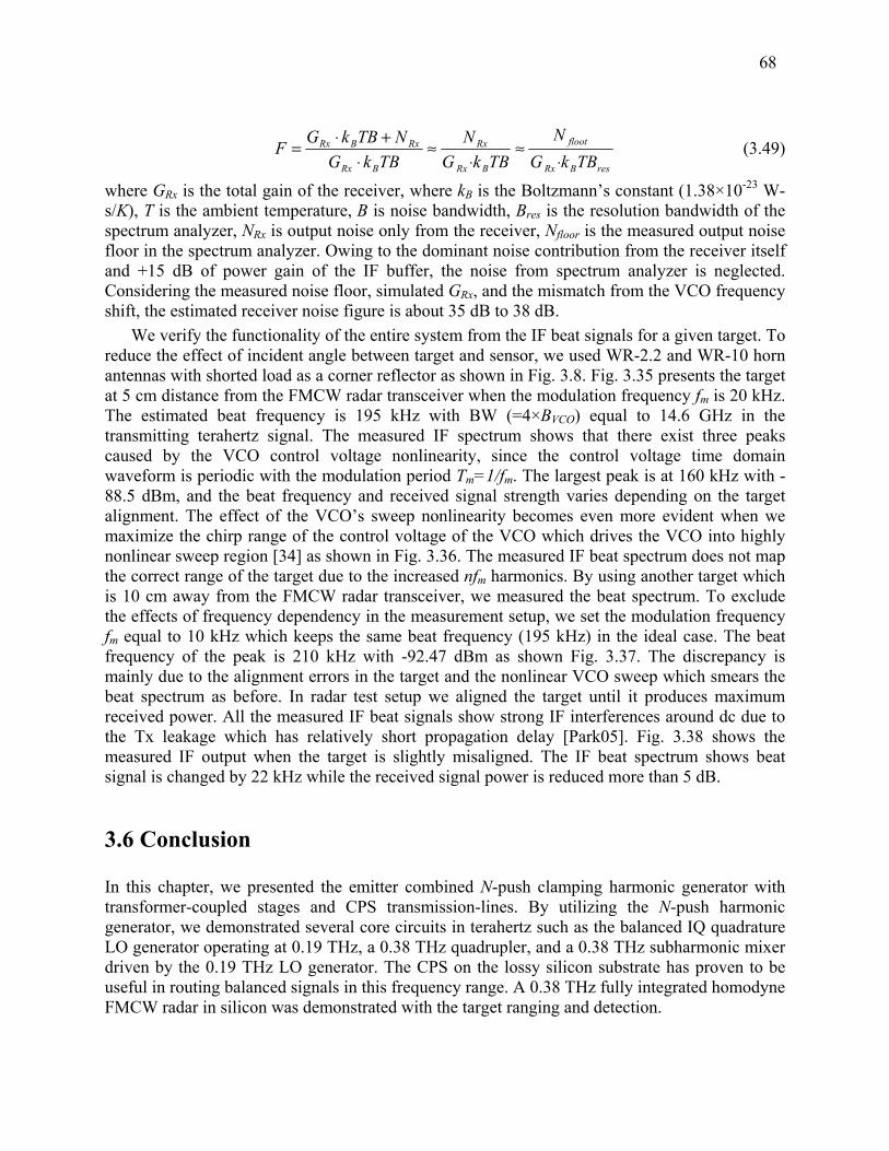
68
resBRx
floot
BRx
Rx
BRx
RxBRx
TBkG
N
TBkG
N
TBkG
NTBkGF
⋅≈
⋅≈
⋅+⋅= (3.49)
where GRx is the total gain of the receiver, where kB is the Boltzmann’s constant (1.38×10⁻²³ W-s/K), T is the ambient temperature, B is noise bandwidth, Bres is the resolution bandwidth of the spectrum analyzer, NRx is output noise only from the receiver, Nfloor is the measured output noise floor in the spectrum analyzer. Owing to the dominant noise contribution from the receiver itself and +15 dB of power gain of the IF buffer, the noise from spectrum analyzer is neglected. Considering the measured noise floor, simulated GRx, and the mismatch from the VCO frequency shift, the estimated receiver noise figure is about 35 dB to 38 dB.
We verify the functionality of the entire system from the IF beat signals for a given target. To reduce the effect of incident angle between target and sensor, we used WR-2.2 and WR-10 horn antennas with shorted load as a corner reflector as shown in Fig. 3.8. Fig. 3.35 presents the target at 5 cm distance from the FMCW radar transceiver when the modulation frequency fm is 20 kHz. The estimated beat frequency is 195 kHz with BW (=4×BVCO) equal to 14.6 GHz in the transmitting terahertz signal. The measured IF spectrum shows that there exist three peaks caused by the VCO control voltage nonlinearity, since the control voltage time domain waveform is periodic with the modulation period Tm=1/fm. The largest peak is at 160 kHz with -88.5 dBm, and the beat frequency and received signal strength varies depending on the target alignment. The effect of the VCO’s sweep nonlinearity becomes even more evident when we maximize the chirp range of the control voltage of the VCO which drives the VCO into highly nonlinear sweep region [34] as shown in Fig. 3.36. The measured IF beat spectrum does not map the correct range of the target due to the increased nfm harmonics. By using another target which is 10 cm away from the FMCW radar transceiver, we measured the beat spectrum. To exclude the effects of frequency dependency in the measurement setup, we set the modulation frequency fm equal to 10 kHz which keeps the same beat frequency (195 kHz) in the ideal case. The beat frequency of the peak is 210 kHz with -92.47 dBm as shown Fig. 3.37. The discrepancy is mainly due to the alignment errors in the target and the nonlinear VCO sweep which smears the beat spectrum as before. In radar test setup we aligned the target until it produces maximum received power. All the measured IF beat signals show strong IF interferences around dc due to the Tx leakage which has relatively short propagation delay [Park05]. Fig. 3.38 shows the measured IF output when the target is slightly misaligned. The IF beat spectrum shows beat signal is changed by 22 kHz while the received signal power is reduced more than 5 dB.
3.6 Conclusion
In this chapter, we presented the emitter combined N-push clamping harmonic generator with transformer-coupled stages and CPS transmission-lines. By utilizing the N-push harmonic generator, we demonstrated several core circuits in terahertz such as the balanced IQ quadrature LO generator operating at 0.19 THz, a 0.38 THz quadrupler, and a 0.38 THz subharmonic mixer driven by the 0.19 THz LO generator. The CPS on the lossy silicon substrate has proven to be useful in routing balanced signals in this frequency range. A 0.38 THz fully integrated homodyne FMCW radar in silicon was demonstrated with the target ranging and detection.

69
Figure 3.32. Measurement setup for the EIRP of the transmitter.
Figure 3.33. Comparison between measured EIRP and simulated output power as a function of the base bias voltage (Both are individually normalized to the maximum value).
Calorimeter Sensor
Erickson Calorimeter(PM-1B)
Chip-On-Board
WR-2.2 to WR-10Transition
WR-2.2 VDI-Diagonal Horn Antenna
Chip-On-Board
0.2 0.4 0.6 0.8 1.0 1.2-10
-9
-8
-7
-6
-5
-4
-3
-2
-1
0
1 Measured N.EIRP Simulation N.Pout
No
rma
lize
d E
IRP
an
d P
ou
t (dB
)
Base Bias Voltage (V)

70
Figure 3.34. Measured EIRP with calorimeter as a function of the VCO tuning voltage.
Figure 3.35. Measured IF output spectrum with a target positioned at normal direction at 5 cm distance from the terahertz FMCW transceiver with fm=20 kHz.
0.0 0.5 1.0 1.5 2.0 2.5 3.0-15.0
-14.5
-14.0
-13.5
-13.0
-12.5
-12.0
-11.5
-11.0
-10.5
-10.0
Mea
sure
d E
IRP
(dB
m)
VCO Tuning Voltage (V)
Meas1 Meas2
IF interference due to Tx leakage
IF signal from the target
nfm harmonics from VCO nonlinearity

71
Figure 3.36. Measured IF output spectrum with the same condition used in Fig. 3.35 with wider frequency chirp in VCO which comes to have highly nonlinear sweep characteristic.
Figure 3.37. Measured IF output with and without a target 10 cm away from the homodye FMCW radar transceiver.
Increased nfm harmonics
IF Interference due to Tx leakage
IF interference due to Tx leakage
IF signal with the corner reflector
IF signal without the target

72
Figure 3.38. Measured IF output when the target is misaligned. Ohterwise the measurement condition is the same with that in Fig. 3.37.
IF interference due to Tx leakage
IF signal with the tilted target
IF signal without the target

73
Chapter 4
A 0.26 THz Fully Integrated CMOS Wireless Transceiver
4.1 Introduction
In this chapter, a short range wireless transceiver at 0.26 THz is presented for chip-to-chip communication. While wired networks become exponentially complex as the network nodes increase, the wireless counterpart can be easily manageable without routing complexity in wired network in a limited area by the virtue of the flexibility of the wireless link. To serve this functionality, such a link, or wireless bus, it should have low latency, high data rate, and reasonable power consumption. This wireless bus can fulfill many roles, especially routing between chips when a physical interconnection is difficult as presented in Fig. 4.1. The terahertz frequencies are interesting in these applications to enable high data rates without incurring a large area penalty. As discussed in Chapter 1, the atmospheric terahertz transmission window with a center frequency around 0.25 THz offers about 100 GHz of bandwidth which is useful for wireless communication. At this frequency range, the dimensions of on-chip antennas become comparable to a few pads, and antenna inefficiency is comparable to signal loss through the pads and the package, making a fully integrated solution the preferred choice. However, realization of fully integrated terahertz transceivers is challenging because the performance of CMOS devices is severely limited at these frequencies. Moreover the Gb/s communication necesscites wideband IF circuits. This chapter demonstrates a terahertz wireless OOK transceiver operating beyond the device cut-off frequency (fT) and maximum oscillation frequency (fmax) by utilizing frequency multipliers and spatial power combining with a leaky-wave on-chip antenna array.
System level design is given in section 4.2. Dual antenna wireless transceiver architecture is discussed in section 4.3, followed by the detailed circuit design for the transmitter and the receiver of the terahertz integrated transceiver are covered in section 4.4 and section 4.5, respectively. In the next section, the dual Tx/Rx on-chip half-width microstrip leaky-wave antenna (MLWA) design is discussed in detail. In section 4.7 the measurement results are presented followed by the conclusion in 4.8.

74
Figure 4.1. Terahertz short range communication for wireless chip to chip interconnection.
4.2 Short Range Communication System
The terahertz communication link has its unique characteristic compared with RF/mm-wave wireless communication link. Due to the large propagation loss of the terahertz signal and relatively low power available from currently available terahertz sources, the communication is usually requires high gain antennas and the system is limited to the line-of-sight link in a short range. In this context terahertz wireless link is suitable for a security communication due to its high attenuation characteristic in atmosphere. This short range wireless transceiver aims at providing a reliable chip to chip communication in a size constrained box or module which would cause multipath fading channel and signal interferences with other wireless transceivers. Therefore the terahertz transceiver should be robust to possible channel fading. Moreover for the transceiver implemented in silicon, the transmitter power and receiver sensitivity is extremely limited. Therefore system level design should be carefully directed to achieve desirable data-link performance.
4.2.1 Required Signal to Noise Ratio
To achieve desired performance, the required signal to noise ratio (SNR) should be met for a given modulation scheme. Based on transmitted power, the aperture size of the transmitter and receiver, and receiver noise figure, we can estimate the received power from the Friss equation assuming non-fading channel calculated by
( ) sa
Rx
la
RxTxTxRx LL
GEIRP
dL
GGPP
⋅==
20/4 λπ
(4.1)
where La is the atmospheric path loss, ( )20/4 λπ ls dL = is the free space path loss, dl is the
communication link range, λ0 is the wavelength of the transmitted signal, PTx is the transmitted power, EIRP=GTxPTx is the effective radiated power, GTx and GRx are the antenna gains for transmitter and receiver, respectively. The atmospheric path loss is negligible in a short range communication. The performance of the digital communication system is specified by the energy per bit to noise power spectral density ratio ( 0Nbε ). The required receiving signal power for a
specific data rate Rb (b/s) is calculated by [Proakis08]

75
⋅⋅=
00)( N
NRP bbreqRx
ε (4.2)
with 0Nbε is determined by the channel and modulation scheme for a given system requirement.
The equivalent input noise energy is given by
SYSBTkN =0 (4.3)
where kB is the Boltzmann’s constant (1.38×10⁻²³ W-s/K), T0 = 290 °K, and TSYS is the equivalent noise temperature of the system which is
RxASYS TTT += (4.4)
where TRx is the equivalent noise temperature of the receiver, and the noise temperature of the receiver antenna is
pradblkradA TTT )1( ηη −+= (4.5)
with ηrad is the radiation efficiency of the antenna, Tp is its physical temperature, and Tblk is the equivalent brightness temperature of the background which can be calculated by [Pozar05]
( ) ( )
( )
= =
= == π
φ
π
θ
π
φ
π
θ
φθθφθ
φθθφθφθ
2
0 0
2
0 0
sin,
sin,,
ddD
ddDT
TB
blk (4.6)
where TB(θ, ϕ) is the distribution of the background temperature, and D(θ, ϕ) is the directivity of the antenna. In short range data-link Tblk can be approximated by Tblk ≈ Tp which results in TA ≈ Tp. The equivalent noise temperature of the receiver is expressed in terms of the noise figure of the receiver.
( ) 01 TFT RxRx −= (4.7)
When TA ≈ Tp, N0 is calculated by
( )( ) 000 1 TFkTFTkTkN RxBRxpBSYSB ≈−+≈= (4.8)
4.2.2 Multiple Antenna Transceiver with Spatial Diversity
Realization of the fully integrated terahertz transceivers is challenging because fT and fmax of the CMOS devices are considerably lower than operating frequency. Because fmax of NMOS device is less than operating frequency, the terahertz signal should be generated with harmonics which makes it difficult to achieve strong enough output power with low conversion efficiency. In order to overcome the performance limitation of the device, multiple antenna transceiver shown in Fig. 4.2 is a good candidate to meet the required SNR which also provides spatial diversity for a possible multipath channel fading in the box. When we consider multiple antenna transmitters spatially combined with each transmitter unit having GUTx of antenna gain, and PUTx of transmitting power, the total EIRP can be calculated as

76
Figure 4.2. Multiple antenna (a) transmitter (b) receiver for the terahertz wireless link.
UUTxUTx EIRPnNPGnEIRP 2=⋅⋅= (4.9)
where n is the number of the arrayed unit chain. The noise factor of the unit receiver chain Fu is given by
UO
UO
UI
UI
U
NS
NS
F = (4.10)
When multiple antenna receiver chains are combined together for the non-fading Gaussian channel, the receiver noise factor F of the M-array transceiver is not changed because noise and signals from each channel are added in the parallel which does not change the signal to noise ratio.
U
UO
UO
UI
UI
F
NSn
NSn
F =
= (4.11)
However, the effective total antenna gain is increased by n which gives
URxarrayRx GnG = (4.12)
Therefore the signal strength of the multiple antenna transceiver gets improved by n3 where the receiver antenna gain improvement is nGURx, and the increased transmitter power is n2EIRPU. Hence the output SNRout of the multiple antenna transceiver is given by
Uoutout SNRnSNR ⋅= 3
(4.13)
From (4.2) and (4.13), the required number of array for the multiple antenna transceiver for the Gaussian channel is calculated by
( ) ( )3
0
02
3)(
2/4/4
⋅
⋅=
⋅=
NGEIRP
NMRdL
GEIRP
MPdLn b
URxU
ba
URxU
reqRxareq
ελπλπ (4.14)
where M is the link margin for the capacity of the communication link.
The transceiver with multiple receiver chains with separate antennas provides spatial diversity gain for fading channels [Proakis08]. The multiple chain transceiver is robust to fading without expanding the bandwidth of the transmitted signal. Hence this multiple receivers become quite appealing strategy to fight against a possible channel fading for reliable chip to chip communication in the box. Considering a strong line of sight signal and multi-path interference,
(a) (b)

77
the area constrained box must be a Rician fading channel. However there is not any information on fading coefficients for receiver as well as transmitter which can be considered as non-coherent Rician fading channel and its effect is studied for M-PSK [Gursoy05].
4.2.3 Modulation Scheme for a terahertz Short Range Communication
The required SNR is a strong function of the modulation scheme. Given a communication range of cm’s, the limited device performance of 65 nm GP CMOS at terahertz frequencies, it is critical to choose an optimal modulation scheme to achieve desired pJ/bit energy efficiency in a short range line-of-sight wireless link. In this section two feasible modulation schemes are considered for terahertz short range communication based on energy efficiency and transceiver complexity.
4.2.3.1 On-Off Keying (OOK)
In a short range date link, OOK modulation scheme has several advantages. Accordingly ‘1’ and ‘0’ are represented by two different transmitting power levels. Therefore OOK modulation is considered as one of the simplest modulation scheme as shown in Fig. 4.3. Because information is directly carried as the amplitude change of the transmitted signal, it provides robustness to carrier frequency shift as well as simple front-end elements. However, it has low bandwidth efficiency and requires relatively high SNR as it is heavily affected by noise and interferences.
4.2.3.1.1 Coherent OOK Receiver In OOK, the signal format is
( )tnTtpnAtx Cn
b ω∞
−∞=
−= cos)(][)( (4.15)
where p(t)=Π(t/Tb) and A[n]∈0, AC.
Let us consider noise level of the coherent OOK case. The received signal and noise passes through a bandpass filter before being down converted to baseband. Therefore the initial white noise becomes a colored bandpass process. For the bandpass process, the detected in-phase and quadrature noise components have following power spectral densities (PSDs)
<++−
== otherwise 0
),()()()( LPFCNCN
NN
ffffGffGfGfG
Qi (4.16)
When f is less than the low-pass filter cut-off frequency fLPF, SYSBNN TkNfGfGQi
=== 0)()( .
In coherent OOK, energy per bit (ɛb) is given by
( ) TAdttA C
T
CCb
b 2
0
22
4
1cos
2
1 == ωε (4.17)
with difference signal energy of the OOK 0, AC, Ed=ɛb/2. By using the optimum threshold setting with matched-filter reception, the bit error rate Pb for binary signaling corrupted by white Gaussian noise is given by

78
=
==
002 NQ
N
EQPP bd
eb
ε (With matched filter) (4.18)
where Marcum Q-function (Q(x)) is defined as
( ) duexQx
u
∞ −
≡ 2
2
2
1
π (4.19)
4.2.3.1.2 Non-Coherent OOK receiver
The OOK receiver can be implementable without any phase synchronization in non-coherent detection scheme though better SNR is required. Depending on the carrier signal status on an AWGN channel, the probability distribution function (PDF) is different. When ‘1’ is transmitted with constant carrier component Ac, the PDF is the Rician given by
≥
+−== otherwise 0
0 ,2
exp)|( 202
22
21
xxA
IAxx
AHxpCC
C σσσ
(4.20)
Where I0 (·) is the modified Bessel function of the first kind with order zero, σ2 is the variance of the noise. For ‘0’ carrier component, the PDF is the Rayleigh function.
0,2
exp)0|(2
2
20 ≥
−== x
xxHxp
σσ (4.21)
For reasonably large SNR (AC>>σ), the Rician function simplifies to the Gaussian distribution with variance σ2, and mean equal to AC given by
( )0,
2exp
2)|(
2
2
21 ≥
−−== xAx
A
xAHxp C
CCy σσπ
(4.22)
Practically high SNR is assumed which results in the threshold is approximately at the half way and the error rate is the average of ‘0’ and ‘1’ reception probabilities
( )0|1|2
1eee PPP += (4.23)
−=
−==
∞
02
2
2/
00| 4exp
8exp)|(
N
AdyHypP bC
A
e
C
εσ (4.24)
Where BN02 =σ , bTrB /22 => ,
bCb TA2
4
1=ε .
( )
=≈=
∞ 0
2/
11| 22/)|(
NQAQdyHypP b
C
A
e
C εσ (4.25)
Therefore, the bit error rate for non-coherent OOK receiver can be calculated as
NNN
QN
PP bbbb
eb >>
−≈
+
−≈= εεεε
,4
exp2
1
24exp
2
1
000
(4.26)

79
Figure 4.3. Schematic diagram of OOK modulation scheme, and its constellation diagram.
It should be noted that (4.26) holds only when 0Nb >>ε .
4.2.3.2 Quadrature phase-shift keying (QPSK)
While OOK modulation provides simple transceiver structure with reasonably reliable link in short range communication, it is vulnerable to jamming or interference signals. Compared with OOK modulation scheme, M-ary phase shift keying (M-PSK) modulates the phase of the carrier to deliver signals which is robust to the interference. QPSK uses four points on the constellation diagram, equi-spaced around a circle. With four phases, QPSK can encode two bits per symbol.
Compared with binary phase-shift keying (BPSK), it can achieve the same data rate of BPSK with half of bandwidth for the same BER. In other way, it achieves twice of the data rate of BPSK with same bandwidth. In this case QPSK requires twice of the transmitting power to maintain the same BER (ɛb/N0) in BPSK case. Therefore QPSK provides twice the spectral efficiency with exactly the same energy efficiency compared with BPSK.
Fig. 4.4 shows the schematic diagram of the QPSK modulation scheme. QPSK can be considered as two BPSK structures (I/Q channels) in parallel, which is easily implementable in integrated circuit which makes QPSK a good candidate. The symbol error probability Pe for the QPSK is given by
−
=
00
2
2
11
22
NQ
NQP bb
e
εε (4.27)
When ɛb/N0 is practically large enough, Pe can be simplified as
≈
0
22
NQP b
e
ε (4.28)
When Gray code is used in the mapping, the equivalent bit error probability for M-ary PSK is well approximated by [Proakis05]
=≈
02
2
log NQ
M
PP be
b
ε (4.29)
This bit error probability of QPSK is the same with BPSK case but, QPSK requires only half of the bandwidth that is required for BPSK.
Data
OutChannel
Data
(0) (+1)BPF

80
Figure 4.4. Schematic diagram of QPSK modulation scheme, and its constellation diagram.
4.2.4 Link Budget Analysis
Based on the design equations for a given modulation scheme, we can estimate required number of array nreq as a function of 0Nbε , data rate Rb, and the equivalent receiver noise N0 calculated
from the receiver noise figure. We draw the equivalent contours of the required number of array elements as a function of the data-link range d in x-axis, and receiver noise figure in y-axis. The number on top of the contour denotes nreq for a given modulation scheme. In those calculations, we assume each array element has -1 dBm of output power, and +2 dBi of the antenna gain based on the designed components and aiming data rate is 20 Gb/s with BER equal to 10-10 with M =+4 dB of link margin considering possible Rician fading channel in the box communication.
Fig. 4.5 presents the required number of array with QPSK. The calculated nreq ranges from 1 to 6 as a function of the link range from 10 mm to 100 mm when NFrx is equal to 20 dB. It should be noted that the M-PSK modulation used in terahertz should meet quite strict phase noise requirement as the output is generated by the frequency multiplier as the phase scales with multiplier factor. Therefore the effect of phase scale should be also considered in baseband processing. Fig. 4.6 shows nreq for coherent OOK modulation. All the condition is same with that of QPSK. When NFrx is equal to 20 dB, nreq ranges from 1 to 8 as a function of the link range from 10 mm to 100 mm. Fig. 4.7 presents nreq for non-coherent OOK modulation. The resulting nreq is almost same for coherent and non-coherent OOK in the range within 20 mm. In terms of power consumption per unit channel, the unit cell of the non-coherent transceiver consumes less power since it does not require a Phase-Locked Loop (PLL). From the contour, we see that nreq =2 for N-OOK modulation scheme when receiver noise figure is better than 20 dB in 15 mm range. The choice of this simple modulation scheme provides enhanced robustness to carrier frequency shift as well as simple front-end and baseband structure. Therefore we choose the non-coherent OOK modulation scheme in this design considering design simplicity and its channel as non-coherent Rician fading channel [Gursoy05].
Based on our analysis, the feasible chip to chip wireless link range is within 50 mm. Compared with the inductive-coupling inter-chip link which requires the link range less than 0.1 mm with a precision alignment of chips over the dielectric layers [Niitsu10], the ultrafast THz wireless link for chip to chip inter-connection has much better flexibility than the reported magnetic coupling inter-chip link.
tCωcos

81
Figure 4.5. Required number of array depending on link range and receiver noise figure for a transceiver with QPSK modulation scheme having -1 dBm of unit output power, and +2 dBi of the unit antenna gain when the desired data rate is 20 Gb/s with BER equal to 10-10 with +4 dB of link margin.
Figure 4.6. Required number of array depending on link range and receiver noise figure for a transceiver with coherent OOK modulation scheme having -1 dBm of unit output power, and +2 dBi of the unit antenna gain when the desired data rate is 20 Gb/s with BER equal to 10-10 with +4 dB of link margin.

82
Figure 4.7. Required number of array depending on link range and receiver noise figure for a transceiver with non-coherent OOK modulation scheme having -1 dBm of unit output power, and +2 dBi of the unit antenna gain when the desired data rate is 20 Gb/s with BER equal to 10-10 with +4 dB of link margin.
4.3 CMOS Terahertz Wireless Transceiver Architecture
In short-range terahertz wireless communication transceiver, it is important to make the front-end structure as simple as possible considering power consumption as we discussed the trade-off between nreq and modulation scheme in section 4.2.4. Although the QPSK modulation scheme requires less number of array elements nreq in the range from 10 mm to 100 mm, it has several disadvantages in this application. Firstly the phase noise requirement of the fundamental signal source is quite stringent as it scales up with the multiplier factor. Secondly, baseband signal processing is required to consider the expansion of the output signal spectrum from the multiplier, while the non-coherent OOK modulation scheme can modulate the output by switching ‘On’ and ‘Off’ directly to the terahertz output. However it is quite undesirable to put an electrical switch at the output considering a large insertion loss in the signal path. Moreover the parasitic capacitances make it impractical to get high enough isolation.
Fig. 4.8 presents the architecture of the designed CMOS terahertz wireless transceiver. Each color box denotes operating frequency for a given block. In transmitter, we use a frequency quadrupler implemented with the quadruple push clamping circuit. We switch the quadrature input of the quadrupler at 65 GHz. Then the output signal of the quadrupler has the same rate of switching speed at 260 GHz. Because we are aiming at data rate (Rb) upto 20 Gb/s which changes the ‘On’ and ‘Off’ status within roughly three periods of the 65 GHz signal, the switching action should be well controlled considering the transient signal ringing caused by the resonant matching networks. The non-coherent OOK modulator is implemented in a distributed

83
fashion to overcome transient signal ringing caused by the resonant matching networks in the Tx chain. A 65 GHz balanced signal (0°, 180°) is generated from the Tx VCO with a differential cascode buffer. Two branch-line hybrids take each of the differential outputs of the Tx VCO and produce the balanced I/Q output signals for respective Tx quadrupler chain. The balanced signals are routed with the coplanar strip-line (CPS) providing better signal integrity and higher common mode rejection with a comparable propagation loss compared to CPW and MSTL counterparts [Gevorgian01].
The receiver consists of two separate channels. Because the fT and fmax of the 65 nm CMOS devices are quite below than 260 GHz, it is impossible to implement a Low Noise Amplifier in the receiver front-end. Therefore it is essential to minimize the NF of the down converting mixer. A double-balanced passive mixer is used for down conversion to achieve high LO to IF isolation. To minimize the noise figure (NF) of the mixer, a strong LO signal is necessary. Two 3rd
harmonic balanced LO signals with +0 dBm power are generated from two triplers biased in class-C. As the switching pair generates a strong fundamental signal, a hair-pin filter is implemented to reject a strong fundamental signal from the tripler output. The triplers are driven by a V-band LO chain consisting of a class-D-1 PA, a hybrid, and Rx VCO. The down-converted IF signals from the two respective mixers are amplified by a wide-band IF driving amplifier utilizing loosely coupled IF transformers to achieve pole-separation. The amplified 65 GHz balanced IF signals are demodulated with a quadruple push structure with RC lowpass filter output load. With this structure, the 65 GHz signal rejection filter is not necessary and the IF signals from two receiving channels are combined in current domain. The output voltage at the low pass filter load is input to the IF buffer to drive external instrument for measurement purpose.
Figure 4.8. Block diagram of designed terahertz CMOS wireless transceiver.
Qu
adru
pler
Qu
adru
pler
Tx VCO
Distributed OOK Modulator
Hybrid
Hybrid
Distributed OOK Modulator
X 3
IF out
Rx VCO
delay line
X 3
195GHz20Gb/s 65GHz 260GHz
+9 dBm
0 dBm -2 dBm
DA
Q180o
Q0o
I0o
I180o
+13 dBm+7 dBm
-1 dBm
-1 dBm
EIRPmax=+6.8 dBm
+13 dBmPA
+4 dBm
+13 dBm
0 dBm
450V/W 10 mVpp
-38 dBm
-38 dBm
-48 dBm-22 dBm
-22 dBm

84
4.4 Transmitter Circuits
In the transceiver circuit design, all the terahertz circuits are designed based on the 3-D EM simulation with the interconnection via structures from top metal to M1, and the transistor models provided by design kit with post-layout extraction using Calibre xRCTM. The rational fitting models are extracted with S-parameters from HFSSTM by using Spice Model Generator in ADS. The simulations are used for the metal stacks and interconnect structures. For millimeter-wave power amplifier and IF amplifiers, two thick metal layers (M8, M9) and related vias are simulated in HFSSTM, and device structures are more relied on the transistor model with post-layout extraction with Calibre-xRCTM.
4.4.1 260 GHz Quadrupler
The transmitter quadrupler is designed using a quadrature-push clamping circuit consisting of two drain-coupled NMOS pairs driven by the balanced IQ quadrature input signals. Different from the BJT case, the hard switching MOS is considered as a resistive switch controlled by gate voltage. The gate bias is provided by the center tap of the transformer. Fig. 4.9 shows the circuit diagram of the quadrupler. Owing to the quadruple push clamping structure, odd harmonics are cancelled out including the strong fundamental driving signals. Therefore bulky and lossy fundamental signal rejection circuit is not necessary. Only n·4th (n=0, 1, 2, ···) harmonic elements are delivered at output load. The line inductance of the VDD is included in the matching network. The series inductor LgM is chosen considering the routing of the balanced I/Q quadrature signals with CPS T-line. The series inductor with the routing length lR of the CPS with Z0=92 Ω (W=8 µm, G=6 µm) simplifies the impedance matching network considering the series inductance from the physical routing of the CPS. The gate dc bias is fed from the center tap of the output transformer in the power amplifier (PA).
The width of the NMOS determines the drain and gate capacitance size as well. Therefore the matching networks are directly affected by the device size. The size must be chosen to achieve desired bandwidth with the trade-off between maximum deliverable output power and the conversion efficiency. When we consider the device as a switch on resistor Ron and capacitor CDS in parallel, the drain to source on-resistance Ron is scaled down by 1/W, and the drain-source capacitance is scaled up by W. Hence ideally the larger device the better output power as well as efficiency. However the devices size is limited by the size of the parasitic capacitances at the drain node which results in narrow band matching network that is sensitive to model inaccuracy and process variation. Moreover, the gate input impedance increases with the device size which can induce higher gate voltage for a given driving power. In this design, the width of M1, M2, M3, and M4 is chosen to be 20 µm. As the load is the spatially combined two half width MLWA with one of the edges shorted to ground, we designed the output matching network with the coupled line having length lc. The coupled line with 2 dB of insertion loss serves as a dc blocker. With two Pin =+13 dBm input signals applied to I and Q push-push pairs, the 2nd harmonic becomes larger than 4th harmonic when the phase mismatch is larger than 10° as presented in Fig. 4.10. Fig. 4.11 shows the output power of the designed quadrupler as a function of total input driving power. When +16 dBm of total input power is driving the quadrupler, the output power is -0.3 dBm at 260 GHz.

85
Figure 4.9. Circuit diagram of the transmitter quadrupler with the quadruple-push harmonic structure.
Figure 4.10. Output harmonics of the transmitter quadrupler as a function of I/Q phase mismatch.
I180°
Arrayedtwo MLWA s
I0°
VDD
MSTL coupled-line at 4th harmonic
gML
gML
gML
gML
M1 M2 M3 M4
Φ
2nd Switch CPS
Q270°
Q90°
Φ
2nd SwitchCPS
Pout
-60 -50 -40 -30 -20 -10 0 10 20 30 40 50 60-50
-40
-30
-20
-10
0
10
20
Qua
d. P
ush
Out
put P
ower
(dB
m)
I/Q Phase Mismatch (degree)
4th Harmonic
1st Harmonic
2nd Harmonic
3rd Harmonic

86
Figure 4.11. Simulated quadrupler output power (Pout) of harmonic components depending on the total input driving power.
4.4.2 V-band Hybrid A quadrature hybrid is designed to generate I and Q signals in the transmitter and split the power in the LO chain of the receiver. There are several approaches to reduce the size of the hybrid, one way is to use the branchline hybrid with capacitive loads [Hirota90], and the other is to implement it with lumped capacitors and transformers [Frye03]. The latter is reported that the size of the hybrid with lumped components can be further reduced than the former [Tabesh11] in 60 GHz. However the branchline hybrid can be used as a part of the routing transmission-line (T-line) which saves areas for the external routing T-line to the lumped hybrid. Fig. 4.12-(c) shows the designed size-reduced MSTL branchline hybrid. The pitch of two output ports is designed to be fit to the input of each channel. The designed size of the hybrid occupies 115×210 µm2 though it serves as a part of the routing T-line. The capacitance loaded T-line is shown in Fig. 4.12-(b). Compared with the desired θ0=π/2 T-line with Z0 in Fig. 4.12-(a), the physical length l= θM/ω of the capacitance loaded T-line can be reduced given by
== −
M
lM
Z
Zl 01sin
4
λω
θ (4.30)
0
cos
ZC M
P ωθ= (4.31)
In the normal branchline hybrid with port impedance Z0, the required characteristic impedance of the horizontal branch T-line is 2/0Z , and that of vertical branch T-line is Z0. To make the
width same for horizontal and vertical T-line to avoid discontinuity of the junction, the length of
-6 -4 -2 0 2 4 6 8 10 12 14 16 18 20 22 24 26-55
-50
-45
-40
-35
-30
-25
-20
-15
-10
-5
0
5
Ou
tpu
t Po
we
r (d
Bm
)
Total Input Power (dBm)
4th Harmonic Fundamental
2nd Harmonic
3rd Harmonic

87
vertical branch is chosen longer. The required capacitance load CT is given by the sum of CH from the horizontal size reduction and CV from the vertical size reduction. Fig. 4.13 presents the S-parameters extracted with HFSS simulation. The insertion loss is around 2 dB with less than 0.4 dB of amplitude mismatch between I and Q, phase mismatch is less than 2° between 60 GHz and 70 GHz as given in Fig. 4.14.
Figure 4.12. (a) Desired θ0=π/2 T-line with Z0, (b) Equivalent size reduced T-line (θM) with ZM , and (c) Structure of the meandered hybrid with capacitive load CT.
Figure 4.13. Simulated S-parameters in dB for the designed size reduced hybrid.
MZ
TC
TC TC
VHT CCC +=
0Z
PC PC
Mθ
20
πθ =
40 45 50 55 60 65 70 75 80-35
-30
-25
-20
-15
-10
-5
0
S-p
ara
me
ters
(d
B)
Frequency (GHz)
S11
S21
S31
S22
S33
S32

88
Figure 4.14. Simulated phases of S21 and S31 for the designed size reduced hybrid.
4.4.3 Distributed Non-coherent OOK Modulator in V-band
In order to achieve non-coherent modulation, we switch off )0( =Φ the quadrature input of the quadrupler when desired bit is ‘0’, and switch on )1( =Φ when it is ‘1’. Therefore output of the quadrupler preserves the modulation spectrum at terahertz radiation frequency. Considering the drain efficiency of the power amplifier (PA), the D-1 PA tank has moderate quality factor around 3, which causes a transient signal ringing that limits the modulation data rate of the transmitter. As we are aiming at data rate Rb upto 20 Gb/s which changes the ‘On’ and ‘Off’ status about three periods of the 65 GHz fundamental signal, a single series-switch between DA and PA is not enough to provide fast settling of the damping signal. By introducing 2nd parallel switch between PA and the quadrupler inputs, we can relief the signal ringing from the On/Off transition even more. Fig. 4.15 presents the structure of the distributed OOK modulator. The dummy load masks the switching action propagation to the preceding stages.
From HB simulation, the isolation between ‘On’ and ‘Off’ of the distributed OOK modulator is larger than 45 dB with insertion loss less than 7 dB including single to differential input balun as shown in Fig. 4.16. Fig. 4.17 presents the modulated signal with Rb=20 Gb/s in transient simulation. As shown in the figure, the input clock signal from the distributed routing itself (Mod. Output) suffers from the pulse distortion due to the limited bandwidth throughout the routing trace. There is small ripple at the beginning of the transition. This distributed OOK modulator was designed together with Siva V Thyagarajan.
40 45 50 55 60 65 70 75 80
-120
-100
-80
-60
-40
I and
Q A
mpl
itude
Mis
mat
ch (
deg)
I and
Q P
hase
Mis
mat
ch (
deg)
Frequency (GHz)
-5
-4
-3
-2
-1
0
1
2
3
4
5

89
Figure 4.15. Circuit diagram of the Transmitter distributed non-coherent OOK modulator.
Figure 4.16. Simulated isolation and thru in dB for the designed distributed non-coherent OOK modulator.
4×
40 50 60 70 80-20
-15
-10
-5
0
Isol
atio
n (d
B)
Th
ru (
dB
)
Total Input Power (dBm)
-60
-55
-50
-45
-40

90
Figure 4.17. Simulated non-coherent OOK modulated output signal of the power amplifier.
4.4.4 V-band D-1 Power Amplifier
As discussed in section 4.4.1, higher EIRP requires larger output power from preceding stages. High drain efficiency necessitates use of switching power amplifiers. In switched amplifier like Class D and E amplifiers, the transistor is considered as a switch rather than voltage controlled current source. With ideal switches, it can achieve 100 % drain efficiency. Class D-1 PA has only one parallel LC tank that can be conveniently absorbed into the output transformer network, and the drain capacitance can be used as a part of the resonator. In a Class D-1 PA, the current through the transistor is a square wave, whereas the output voltage is sinusoidal due to the parallel resonant network. A high loaded quality factor QL=ωRLCtank is desirable to achieve high drain efficiency. With the lower QL, the higher order odd harmonic currents dissipate through the parallel RL which results in degradation of the drain efficiency (ηd). When we consider the harmonic leakage as the only loss in the switched amplifier, ηd is given by [Hung05]
∞
= ⋅++⋅
++
=
122 ))12((1
1
)12(
11
1
n L
d
Qnn
η (4.32)
0 1 2 3 4 5
0.0
0.5
1.0P
RB
S
0 1 2 3 4 5-0.6-0.30.00.30.6
Mod
. O
utpu
t (V
)
0 1 2 3 4 5-1.5
0.0
1.5
SW
.Out
put
(V)
T ime (nsec)

91
Therefore it is desirable to get as high Ctank as possible in the ideal case. However, practically the size of the device is limited by the corresponding transformer efficiency used in the tank. The transformer efficiency ηxfm is given by [Aoki02]
2
22
2
///
/
nRQ
L
Q
L
kL
nRQL
nR
Ls
p
p
p
p
Lsp
Lxfm
++⋅
+=
ωωω
ωη (4.33)
where inductor Lp and quality factor Qp are for the primary, Ls and Qs are for the secondary inductor, coupling factor k and truns ratio n. Fig. 4.18 shows the circuit diagram of the Class D-1 power amplifier. The drain capacitances are used as a part of the resonator. The size W=140 µm of the differential switches (M1 and M2) is chosen to provide optimal drain efficiency and power added efficiency as a function of tank capacitance ratio and switch scaling factor as shown in Fig. 4.19 and Fig. 4.20 where tank capacitance ratio is actual tank capacitance to nominal tank capacitance which is required to resonate tank inductance from designed low loss transformer. And switch scaling factor is the switch size in microns divided by 2 µm. i.e. the total switch size is the switch scaling factor multiplied by 2 µm width device.
Class A driver stage is used to control driving amplitude for an optimal switching input power. Simulated output power is +13 dBm when driving input power is +7 dBm for the hard switching. The drain efficiency is 29 % and the power added efficiency is 26 %. The loss is mainly caused by the moderate quality factor Q in the tank circuit. This class D-1 PA was contributed by Siva V Thyagarajan.
Figure 4.18. Schematic diagram of Class D-1 power amplifier.
BV
DDV

92
Figure 4.19. Drain efficiency as a function of tank capacitance ratio and switch scaling factor.
Figure 4.20. Output power as a function of tank capacitance ratio and switch scaling factor.

93
4.4.5 PRBS Generator
High-speed pseudo random binary sequence (PRBS) generator is integrated into the terahertz wireless transceiver to measure the bit error rate (BER) performance up to 20 Gb/s. An external equipment for data stream in this data rate is hard to achieve due to large amount of losses at interconnections. Even for an on-chip PRBS generator, signal distributing higher than 10 Gb/s stream on-chip is quite lossy, and it requires use of repeaters to preserve the rectangular waveform. Owing to its high data rates, current mode logic (CML) type latches and buffers are used.
As shown in Fig. 4.21, interleaved linear feedback shift register and multiplexing architecture is used with 7 consecutive latches for generating PRBS (27-1) with clock frequency 10 GHz. This architecture produces a sequence of length 127 according to the characteristic polynomial x7+x6+1 [Weiss06]. Fig. 4.22 shows the circuit diagrams of the CML components. Implemented with the distributed OOK modulator, high speed data distribution was another limiting factor for high speed data modulation. The residual delay from the CMOS repeater should be minimized to track switching signal synchronization. The circuit was designed to have less than fan-out of 2 to achieve the speed requirement. In order to prevent CML-to-CMOS metastability, a 46 kΩ resistor is connected between input and output of the first CMOS inverter.
The spectral line of the PRBS output has sinc2( f ) envelope having spectral null at m·Rb Hz, m=1, 2, 3 ⋅⋅⋅ . Owing to the pseudo random characteristic which repeats with 2x-1 bits, we can expect the periodic spectral line spacing ∆f Hz given by
12 −=Δ
xbR
f (4.34)
where Rb is the generated data rate, x is the indicates the length of the interleaved latch used to create the pattern interleaved latch. The PRBS generator block was contributed by Shinwon Kang.
Figure 4.21. Schematic diagram of the PRBS generator with interleaved architecture.
Ωk 64

94
Figure 4.22 circuit diagrams of the CML components used in the PRBS generator.
4.5 Receiver Circuits
4.5.1 195 GHz Tripler
A strong 3rd harmonic LO signal (fLO=195 GHz) is necessary to minimize noise figure of the down converter mixer as given in Fig. 4.23 In order to generate a strong odd harmonic, pseudo-differential pair is used which rejects the even harmonics. However, there exists a strong fundamental signal which can leak through the double balanced mixer. In order to reject the undesired fundamental signal, each output is connected to the microstrip T-line (MSTL) hair-pin band pass filter which blocks dc path. By folding the parallel coupled 2/lλ wavelength resonator
into “U” shape, the hairpin resonator is obtained. The differential output from two hairpin filter
Ω500 Ω500
μ3 μ3
μ9
μ6 μ6
μ9
μ19
Φ Φ
μ9
μ19
Φ
Ω500 Ω500
μ4
μ9Φ
μ4 μ4 μ4
Ω500 Ω500
μ8
μ19
μ8
μ9
μ19
Ω500 Ω500
μ4
μ9
μ4 μ4 μ4

95
is routed through Z0=87 Ω (at 195 GHz) CPS T-line (W=8 µm, G=6 µm) to the LO port of the mixer. Fig. 4.24 shows the frequency response of the hair pin filter from HFSS simulation. The insertion loss is less than 2 dB, and the fundamental signal is rejected by -10 dB. When the input driving signal at f0 is strong enough, M1 and M2 are switching abruptly which results in a rectangular voltage waveform at drain nodes which produces abundant odd harmonics while even harmonics are cancelled out.
In order to achieve better conversion efficiency to 3rd harmonic, the output impedance of the fundamental signal should be low enough while the differential output impedance looking into the switching pair at the 3rd harmonic should be matched to the input impedance of the hair-pin filter. The output matching network consisting of a series line-inductor with high Z0 CPS1 and LdM provide matched impedance to the hair-pin filter. The LdM is implemented with a loop inductor connected in parallel, and the center tap is connected to the VDD.
Fig. 4.25 presents output power for each harmonic component. As input power increases, the devices are acting close to ideal switches which produce the output voltage closer to rectangular waveform. Therefore the odd harmonics get increased more with stronger input power as shown. In this design with M1=M2=20 µm, it shows that the output power of the third harmonic saturates around +13 dBm of the driving input power.
Figure 4.23. Circuit diagram of the receiver LO tripler with balanced hair pin filters.
gML
dML dML
DDV
03ffp =
gML MC

96
Figure 4.24. Simulated differential S21 and S11 in dB for the balanced hairpin filter.
Figure 4.25. Simulated tripler output power of harmonic components depending on the input driving power.
50 100 150 200 250 300 350-35
-30
-25
-20
-15
-10
-5
0
S-p
ara
me
ters
(d
B)
Frequency (GHz)
S21
S11
-4 -2 0 2 4 6 8 10 12 14 16 18 20-90
-80
-70
-60
-50
-40
-30
-20
-10
0
10
Ou
tpu
t P
ow
er
(dB
m)
Total Input Power (dBm)
Fundamental
2nd Harmonic
3rd Harmonic
4th Harmonic

97
4.5.2 Demodulator
High speed square-law detector is used for the receiver demodulator whose demodulated output voltage is proportional to the input power. The square-law detector was designed using two push-push clamping NMOS pairs driven by down converted balanced signals from two channels as presented in Fig. 4.26. The width of M1 to M4 was chosen to W=20 µm considering the matching network for the gate input driving stage. Rbias=245 Ω provides gate bias of the following IF buffer for an external measurement. The demodulated IF currents from two channels are combined in current domain and produce a desired square-law output voltage. The push-push structure rejects undesired fundamental signals at output. Therefore a bulky fundamental signal rejection circuit is not necessary. Fig. 4.27 shows peak output voltage of the demodulated signal as a function of input power. The designed demodulator has 849 V/W to 740 V/W of responsivities depending on the total input power from the two differential inputs. Undesired super harmonic components caused by the push-push structure are filtered out with with Cout. The demodulated signal is amplified by the external driving buffer. Rbias is chosen to provide the gate bias of the cascode buffer for external measurement. All the NMOS devices (M1 to M4) are biased at the device threshold voltage to maximize conversion efficiency. For the input matching purpose, the series inductor LgM is chosen considering the routing inductance of the balanced signals with 92 Ω CPS T-line (W=8 µm, G=6 µm). With the series inductor having the routing length lR of the CPS, the parallel 54 fF of MOM capacitor is used to provide impedance matching between output of the IF amplifier and the input of the demodulator. The dc gate bias is fed from the center tap of the output transformer in the wideband IF amplifier. Fig. 4.28 shows the demodulated output waveform when 20 Gb/s OOK modulated input signal is applied.
Figure 4.26. Circuit diagram of the receiver demodulator with two push-push structures.
DDV
gML
gML
gML
gML
M1 M2 M3 M4CPS CPS
Out
I0°
I180°
Q0°
Q180°
MCMC
biasR outC

98
Figure 4.27. Output voltage of the demodulated signals and fundamental signal leakage from the square law demodulator as a function of the total input power.
Figure 4.28. Demodulated output voltage waveform with 20 Gb/s OOK modulated input signal.
0.00 0.04 0.08 0.12 0.16 0.20-0.02
0.00
0.02
0.04
0.06
0.08
0.10
0.12
0.14
0.16
Out
put
Vol
tage
(V
pp)
Total Input Power (mW)
Output voltage of demodulated signal Output voltage at fundamental frequency
0.0 0.5 1.0 1.5 2.00.30
0.35
0.40
0.45
0.50
0.55
0.60
0.65
0.70
Vol
tage
(V
)
Time (nsec)
Demod. Output IF Input

99
4.5.3 260 GHz Double Balanced Mixer
Without any low noise amplifier (LNA) in the receiver, the noise figure of the mixer is critical factor in the receiver performance. For a passive mixer, switching action of the device is directly related to conversion loss and noise figure. In our design, the cut-off frequency fT =160 GHz of 65 nm NMOS is much lower than RF input frequency. However modulation of the transconductance of the NMOS is still possible owing to the distributed nature of the FET channel which is known as Dyakonov-Shur plasmonic mixing in the non-resonant limit [Dyakonov96M] [Lisauskas09]. Only small portion of the channel serves in rectification, and rest of the channel merely works as the extra gate-drain capacitance. Hence the NMOS with fT less than switching LO frequency is considered as the NMOS having an effective gate length (Lgeff) much shorter than physical gate length (Lg) with an effective gate-drain capacitance larger than that at the frequency lower than device fT which could severely degrade the LO to IF isolation. To prevent this adverse effect, we choose the double balanced passive mixer to get high LO to IF isolation.
Fig. 4.29 presents the designed double balanced mixer. To drive two switching pairs (M1, M2) and (M3, M4), a strong LO driving power is essential. Because the harmonic power quadratically decreases with harmonic order, the heterodyne receiver having 65 GHz IF center frequency is chosen with 195 GHz LO frequency. This hetrodyne IF prevents effect of 1/f noise of the passive mixer. From designed frequency multipliers, the conversion efficiency of the tripler is about 6 dB better than that of the quadrupler. In this receiver +0 dBm of 195 GHz differential LO signal drives the designed double balanced mixer, and an overlay transformer is used to couple the balanced LO signal into the gates of the switching devices.
The double balanced mixer has differential input ports (RF+ and RF-). In combing the received RF signal, each source of the two source coupled pair is connected to the arrayed two MWLA while one of the source has λl/2 line to achieve differential signal combining of the receiving signals from two MLWA antennas. The drains are connected to the transformer to achieve impedance matching at differential IF port. It is essential to minimize the NF of the down converting mixer which determines the entire receiver noise figure. Fig. 4.30 presents the conversion loss and noise figure of the double balanced mixer as a function of the LO driving power. When the balanced LO driving power is +0 dBm at 3·f0, the designed double balanced mixer can achieve about 9.5 dB of conversion gain and 14.5 dB of noise figure. This double balanced mixer was designed together with Shinwon Kang.

100
Figure 4.29. Circuit diagram of the down converting mixer with two push-push structures.
Figure 4.30. Simulated conversion gain and noise figure as a function of LO driving power.

101
4.5.4 V-band Wideband IF Amplifier
Since the terahertz receiver does not have a low noise amplifier at the front-end due to the limitation of the CMOS performance, the IF amplifier needs to provide high power gain with high bandwidth with moderate noise figure. Fig. 4.31 presents the designed IF amplifier. The first stage of the IF amplifier uses inductive degeneration structure to achieve low noise matching [Andreani01]. Four consecutive stage cascode amplifiers provide the required gain. With data rate upto 20 Gb/s, the bandwidth of the IF amplifier should be wide enough. To achieve flat band response, each inter-stage is loosely coupled through a double-tuned transformer as shown in Fig. 4.31. The double-tuned magnetically coupled circuit has bandpass transfer function with four poles and a single zero at the origin. Low-coupling coefficient transformers allow pole separation to achieve high bandwidth [Nelson32] [Vecchi11]. The voltage gain of an interstage amplifier (vno/ vni) is given by [Smith97]
)())(1( 012
23
342/1
212
21
asasasasCCk
skgA m
nv ++++−= ωω (4.35)
where
11
1
1
CL=ω (4.36)
22
2
1
CL=ω (4.37)
2
22
21
0 1 ka
−= ωω
(4.38)
)1()1( 21
122
22
221
1 kQkQa
−+
−= ωωωω
(4.39)
2
2
1
13 QQ
aωω += (4.40)
with the quality factors for primary (Q1) and secondary (Q2) inductors are given by
1111
11
2||
L
gR
L
RQ ds
p
ωω== (4.41)
2222
22
||
L
RR
L
RQ Ls
ωω== (4.42)
For the maximally flat response, the coupling coefficient is chosen to Q1 , with 21 QQQ == . The simulated available power gain is 27 dB with 13.5 dB of 3 dB bandwidth, the NF is about 7 dB at 60 GHz with input impedance of 100 ohm. Fig. 4.32 shows the simulated output signal waveform with OOK modulated 60 GHz signal with 10 Gb/s data rate. This IF amplifier was designed together with Siva V Thyagarajan.

102
Figure 4.31. Schematic diagram of the wideband IF amplifier with loosely coupled transformer interstage matching circuits.
Figure 4.32. Simulated output signal waveform with non-coherent OOK modulated 60 GHz signal with 10 Gb/s data rate.
low k
Demodulator
Out+
Out-
2 3 4 5
In+
Out+
Low k
1C 2C 2R1R
A double-tuned magnetically coupled circuit
Si
Si
2nov+
2nov−
2niv+2niv−
0 2 4 6 8 10 12 14
0.0
0.5
1.0
PR
BS
0 2 4 6 8 10 12 14-3-2-10123
Inp
ut
(mV
)
0 2 4 6 8 10 12 14-40-30-20-10
010203040
Ou
tpu
t (m
V)
Time (nsec)

103
4.5.5 V-band Voltage Controlled Oscillator
For the V-band fundamental signal generation, a cross-coupled LC voltage controlled oscillator with cascade output is used [Berney06] [Grebennikov07]. The cascade buffer isolates the LC tank from external load which reduces pulling effect of the VCO as shown in the circuit diagram in Fig. 4.33. Simulated output power is -3 to -2.2 dBm, and the tuning bandwidth is about 6.5 GHz with center frequency at 62 GHz. Fig. 4.34 shows the measured in situ frequency tuning characteristic of the VCO with the setup presented in Fig. 4.41. The measured center frequency is 65 GHz with 5.5 GHz of the tuning bandwidth. This VCO was contributed by Shinwon Kang.
Figure 4.33. Circuit diagram of the VCO with a cascade buffer.
Figure 4.34. Measured Sweep frequency of Tx and Rx VCO as a function of the control voltage.
DDV
-0.25 0.00 0.25 0.50 0.75 1.00 1.25 1.50 1.7561
62
63
64
65
66
67
68 Tx VCO Rx VCO
VC
O fr
eque
ncy
(GH
z)
Control Voltage (V)

104
4.6 Tx/Rx Dual On-chip Antenna Design
In Chapter 2, we discussed that microstrip structure antenna is appealing for integrated on-chip antenna as the ground plane of the antenna can isolate lossy silicon substrate from the signal. In a patch antenna, the bandwidth, efficiency, and gain are limited due to thin IMD height and the standing-wave antenna nature. To overcome those issues, we designed a half width microsrtip leakwave antenna (MLWA). In this section, we design Tx/Rx dual half-width MLWA with wide bandwidth for the Gb/s wireless transceiver by using designed MLWA in Chapter 2.
4.6.1 Half-width Microstrip Leaky-wave Antenna
In order to improve the antenna bandwidth for an ultrafast communications, our approach is to implement a traveling-wave type antenna which are characterized by the matched terminations. In this design, we use a half-width Microstrip Leaky-Wave Antenna (MLWA) which has a ground plane below the signal line, so that the substrate effect is minimized in radiation efficiency degradation. By using 1st higher mode (EH1) which is radiation mode, it has slightly better radiation efficiency than the patch antenna as shown in Fig. 2.9. Owing to its traveling-wave characteristic, the bandwidth is higher than that of the patch antenna. Moreover, high antenna gain can be more easily achievable by using longer transmission-line in a certain boundary. Therefore we can achieve larger aperture which results in higher antenna gain in unit-element. We use the designed half-width leaky-wave antenna in Chapter 2 as the antenna unit element. By placing a metal wall attached to one side of edge, the microstrip-line with λg/4 width excites the 1st higher mode (EH1) as the radiation mode.
4.6.2 Tx/Rx Dual Half-width MLWA
Considering the functionality of the termination which prevents the standing-wave in the transmission-line, the termination can be considered as another input port with impedance matching. We design a half-wave MLWA which simultaneously serves as Tx and Rx dual antenna whose termination is matched to the input impedance of the off-state counterparts. It should be noted that the impedance of the termination seen from the antenna side must provide low enough reflection coefficient. Fig. 4.35 presents the Tx/Rx dual MLWA array structure with four leaky-wave antenna unit elements. There are four MLWA units (A, B, C, D). The antenna unit pair (A, B) and (C, D) serves as two separate antenna elements for TRx_unit1 and TRx_unit2, respectively, each of them are separated by d=λ0/2 (625 µm) to achieve low enough correlation coefficient for the higher spatial diversity gain. The designed antenna achieves comparable radiation efficiency with a patch antenna while achieving 5-6 times wider frequency bandwidth. As the Tx and Rx share the MLWA array, it relieves aperture size restriction due to the chip area constraint, while obviating the need for an explicit TR switch. By arraying four elements, we achieve 4.9 dBi of gain with more than 30 GHz of BW and 26.3% of radiation efficiency at 240 GHz in HFSS. The radiation efficiency decreases as radiation pattern changes to end-fire as frequency goes higher. The simulated radiation pattern is shown in Fig. 4.36. The transmitter and receiver input impedances of the dual MLWA array are shown in Fig. 4.37.

105
Figure 4.35. Structure of the four-elements arrayed Tx/Rx dual leaky-wave antenna.
Figure 4.36. Simulated radiation pattern (Gain) of the designed half-width microstrip leaky-wave antenna array as a function of the radiation frequency.
l=12
50
m
reqε
-25-20-15-10-505
100
30
60
90
120
150
180
210
240
270
300
330
-25-20-15-10-505
10
-25-20-15-10-505
100
30
60
90
120
150
180
210
240
270
300
330
-25-20-15-10-505
10
-25-20-15-10-505
100
30
60
90
120
150
180
210
240
270
300
330
-25-20-15-10-505
10
-25-20-15-10-505
100
30
60
90
120
150
180
210
240
270
300
330
-25-20-15-10-505
10
260GHz
270GHz
245GHz
250GHz

106
Figure 4.37. Simulated return loss of the designed half-width microstrip leaky-wave antenna array as a function of the radiation frequency.
Figure 4.38. Microphotograph of the fabricated fully integrated 0.26 THz CMOS wireless transceiver in TSMC 65 nm digital CMOS process (Dimension: 4.0×1.5 mm2).
220 240 260 280 300-25
-20
-15
-10
-5
0
Ret
urn
Loss
(dB
)
Frequency (GHz)
S11 of Tx Antenna with Tx off
S11 of Rx Antenna with Rx off
Tx/Rx dual AntennaLO PA/ DA/VCO
1st I-PA/ DA/Mod.
Transmitter
Mixer/IFAMP-I
1st Q-PA/ DA/Mod.
2nd I-PA/ DA/Mod.
2nd Q-PA/DA/Mod. Mixer/IFAMP-Q
LO PA/ DA-I
LO PA/ DA-QVCO/DA/Hybrid
X4
X4
Demod.
Filter/X3
Filter/X3
Receiver

107
4.7 Measurement
The 65 nm GP test-chip integrating the proposed transceiver measures 4×1.5mm2 as shown in Fig. 4.38. Using a calorimeter, WR-3.4 horn antenna, and a waveguide transition, we measured +5 dBm of EIRP at 260 GHz. The measurement setup is presented in Fig. 4.39. We measure the radiation pattern of the transceiver by measuring the EIRP as a function of the angle in H-plane. When we compare the measured and simulated antenna pattern, it is clear that the 3rd harmonic affected the radiation pattern measurement since the waveguide cutoff is at fc =174 GHz as shown in Fig. 4.40. We measured the weakly radiating V-band fundamental signal while the transceiver was operating as presented in Fig. 4.41. The in-situ VCO in the transceiver was characterized using a V-band horn antenna, a down-converter, and a spectrum analyzer. For the down converter, V-band LO signal was generated from an external frequency multiplier with an external microwave signal generator. Fig. 4.42 shows the spectrum of the in-situ modulated V-band signal at 14 Gb/s. A wireless data-link was verified over a 40 mm range with the setup as shown in Fig. 4.43, and the spectrum of the 6 Gb/s demodulated toggling signal is shown in the Fig. 4.44. The terahertz link was disrupted by a thin absorber and the link was totally lost as shown in the measured spectrum.
Figure 4.39. Measurement setup for the Equivalent Isotropically Radiated Power (EIRP) of the transmitter.

108
Figure 4.40. Measured Radiation Pattern in H-plane at 0.246 THz.
Figure 4.41. Measurement setup for the spectrum of the transmitter at fundamental frequency.
-30-25-20-15-10-505
100
30
60
90
120
150
180
210
240
270
300
330
-30-25-20-15-10-505
10
H-plane
Measured PRX
(rescaled to GMAX
of H-plane)

109
Figure 4.42. Measured spectral spacing at the fundamental signal with modulation frequency of 14 Gb/s.
Figure 4.43. Test setup for the short range wireless communication link.

110
Figure 4.44. The measured spectrum of the 6 Gb/s demodulated toggling signal with and without blocking the terahertz channel by using a thin absorber.
4.8 Conclusion
A 0.26 THz fully integrated non-coherent OOK transceiver is presented in 65 nm CMOS. The spatially combined dual transceiver architecture with Tx/Rx dual antenna demonstrates +5 dBm of EIRP at fr=0.246 THz and terahertz link with 10 Gb/s toggling signal transfer at 40 mm distance showing the feasibility of terahertz systems operating beyond the cut-off frequency in a digital CMOS technology.
Demodulated Signal
THz Link blocked w/an Absorber

111
Chapter 5
Conclusion
5.1 Thesis Summary
Originating from the unique characteristics of terahertz radiation positioned between photonics and microwave electronics, the terahertz has shown enormous possibility in sensing and communications. Low-cost portable sensors for security imaging and bio-medical applications will improve our quality of life. Ultra wide-bandwidth available in the lower terahertz region can expand our limited spectrum resources. Recently terahertz microelectronics has been spotlighted as emerging technology with advancement of silicon integrated circuit technology. In order to explore the feasibility of terahertz integrated circuits in silicon technology, we have implemented two terahertz transceivers for the FMCW radar sensor and the short range wireless link in well matured conventional 0.13 µm BiCMOS and 65 nm digital CMOS technology, respectively.
While silicon technology is promising solution for low-cost terahertz applications integrated with analog interface circuits and complex baseband logic blocks on chip, the advanced silicon process is very challenging to be used in terahertz applications considering its limited active and passive device performance compared with III-V compound semiconductor or photonic devices. This thesis mainly dealt with how to overcome these limitations.
We have seen that high gain on-chip antenna is the key-role component which can cover up the weak output power in the terahertz transmitter and the low sensitivity in the terahertz receiver. In the nanoscale digital silicon process which has the conductive substrate and the thin inter-metal dielectric (IMD) layers, there are three main loss mechanisms which degrade radiation efficiency. The lossy substrate causes large resistive loss, and the high permittivity of silicon substrate results in the surface-wave mode excitation. To eliminate lossy signal coupling with the silicon substrate, we studied microstrip antennas which have a wide ground plane at the bottom. The two microstrip on-chip antennas were briefly analyzed for two generic silicon processes. For this type of antenna, the thin IMD layers limit the space-wave power radiation when radiating frequency is lower than 300 GHz. In terahertz range, patch antenna can provides relatively high radatiaion efficiency but the bandwidth is very narrow due to the thin IMD layers. A half-width leaky wave antenna was investigated to overcome the limited bandwidth and low radiation efficiency at THz range, but the spatial beam coverage should be taken into account.

112
With limited active device performance, optimal harmonic generation is essential. We implemented a fully integrated terahertz transceiver with N-push clamping circuits with transformer coupled architecture whose driving balanced signals are routed through the coplanar stripline (CPS). The N-push clamping circuit is briefly analyzed with a simplified BJT model for an optimal efficiency. In the hard switching condition, optimal bias condition was derived. The CPS was characterized depending on geometry parameters with 3-D EM simulations. Tx and Rx on-chip rectangular patch antennas with GTx=6.3 dBi and GRx=6.6 dBi were implemented based on the analysis in Chapter 2. Utilizing a push-push pair, a 1:1 overlay transformer, and CPS as the basic building block for the harmonic generation, one can effectively eliminate the fundamental signal, all the even-harmonic generators and subharmonic mixer are designed and integrated with on-chip rectangular patch antenna. Implemented with 0.13 µm SiGe BiCMOS process with device fT=0.23 THz, a 0.38 THz fully integrated homodyne FMCW radar was demonstrated with ranging and detection of a corner reflector target at 10 cm.
A terahertz short range wireless link for the chip to chip communication was presented. A fully integrated non-coherent OOK transceiver is demonstrated in 65 nm digital CMOS process. In order to overcome the inferior performance of the 65 nm CMOS in terahertz regime, the terahertz transceiver utilized spatially combined dual transceiver architecture which is robust to the possible Rician fading channel in the area constrained box. Aiming at short range wireless link, system level design was presented with link budget analysis as a function of the link range and receiver noise figure for non-coherent OOK, coherent OOK, and QPSK modulation schemes. Tx/Rx dual on-chip antenna was presented by using the half-width MLWA while obviating the need for an explicit TR switch. The implemented dual chain transceiver demonstrated +5 dBm of EIRP at fr=0.246 THz and terahertz link with 10 Gb/s toggling signal transfer at 40 mm distance.
5.2 Future Directions
While we have demonstrated the feasibility of the silicon terahertz transceivers with two design examples with well-matured BiCMOS and CMOS technologies, there exists a tremendous amount of research efforts to be dedicated for better performance in on-chip antenna, circuit, transceiver, and system level design at terahertz regime.
In Chapter 2, we have shown that the microstrip structure can achieve the radiation efficiency larger than 50 % in terahertz regime. However the microstrip rectangular patch antenna has narrow bandwidth due to the thin IMD layers of the nano CMOS technology which limits its usage in narrow band applications. Although the MLWA can achieve much wider bandwidth than the patch antenna, the dependence of the main beam direction on the radiation frequency constrains the operating frequency range as well as the achievable antenna gain. A wideband patch antenna can be achievable with E-shape patch antenna [Yang01] by compromising between frequency bandwidth and radiation efficiency when the radiation frequency increases.
In Chapter 3, we discussed that a harmonic generator utilizing nonlinear resistance has the limited conversion efficiency with 1/k2 for kth harmonic component. The harmonic generation with nonlinear reactance can achieve higher conversion efficiency; theoretically zero conversion loss if there is no parasitic resistance. The varactor diode can be a good source of nonlinear reactance. The conversion efficiency will be a strong function of the quality factor Q of the

113
varactor. For the terahertz FMCW radar transceiver, more than 20 GHz of FM sweep is achievable which can achieve 3.75 mm of range resolution for an ideal case. To fully utilize such a wide FM sweep bandwidth, VCO linearization is essential. There are several reported FM chirp linearization methods suitable for integrated circuits [Mitomo10] [Lee10] but have their limitations in achieving a wideband linear FM sweep. Delay-line based compensation can be applied to the correction of the wide sweep bandwidth [Vossiek96]. By picking up the frequency variation ratio using a reference delay line and a mixer, the IF beat signal can be signal processed to correct the phase noise and sweep nonlinearity of the source.
In Chapter 4, we used non-coherent OOK modulation considering the simplicity of the transceiver, power efficiency, and partly because of the lack of an available terahertz channel model for the short range terahertz data-link in the box. As a future work, characterization of the channel in the area constrained box is essential for the coherent modulation scheme such as M- PSK which has better spectral efficiency with less required SNR compared with the non-coherent OOK scheme. For the ultrafast communication, the transceiver requires wideband IF amplifiers. The designed double-tuned transformer coupled IF amplifier in the prototype transceiver mainly limited the achievable data rate. In order to achieve a wider IF bandwidth, a distributed amplifier can be a good choice. However the tradeoff between the gain and power consumption should be optimized in system level design since the distributed amplifier consumes relatively large amount of dc current.

114
Bibliography
[Ahamdi07] M. R. N. Ahamdi et al., “On-chip antennas for 24, 60, and 77 GHz single package transceivers on low resistivity silicon substrate,” IEEE Antennas and Propagation International Symposium, June 2007, pp. 5059-5062.
[Ajito09] Katsuhiro Ajito et al., “Terahertz Spectroscopy Technology for Molecular Networks,” NTT Technical Review, Vol.7, No.3, pp. 1-5, Mar. 2009.
[Alexopoulos83] N. Alexopoulos et al., “Substrate Optimization for Integrated Circuit Antennas,” IEEE Transactions on Microwave Theory and Techniques, Vol. MTT-31, No.7, July 1983.
[Andreani01] Pietro Andreani, and Henrik Sjöland, “Noise Optimization of an Inductively Degenerated CMOS Low Noise Amplifier,” IEEE Transactions on Circuits and Systems. II, Vol. 48, No. 9, pp. 835-841, Sept. 2001.
[Aoki02] I. Aoki et al., “Distributed active transformer-a new power combining and impedance-transformation technique,” Transactions on Microwave Theory and Techniques, Vol. 50, No. 1, Jan. 2002.
[Auth08] Chris Auth et al., “45nm High-k+Metal Gate Strain-Enhanced Transistors,” Intel Technology Journal, Vol. 12, pp. 77-85, June 2008.
[Aziz03] Abdel-Aziz et al., “Design, implementation and measurement of 26.6 GHz patch antenna using MEMS technology,” IEEE Antennas and Propagation Society International Symposium, June 2003, pp. 399-402.
[Babakhani06] A. Babakhani et al., “A 77-GHz Phased-Array Transceiver With On-Chip Antennas in Silicon: Receiver and Antennas,” IEEE Journal of Solid-State Circuits, Vol. 41, pp. 2895-2806, Dec. 2006.
[Baeyens03] Y. Baeyens and Y. K. Chen, “A monolithic integrated 150-GHz SiGe HBT push–push VCO with simultaneous differential V-band output,” in Proc. IEEE MTT-S Technical Digest, 2003, pp. 877–880.
[Bahl80] I. J. Bahl, and P.Bhartia, Microstrip Antennas, Artech House, Dedham, MA, 1980.

115
[Bahl82] I.J. Bahl, and P.Bhartia, and S.S. Stuchly, “Design of Microstrip Antennas Covered with a Dielectric Layer,” IEEE Transactions on Antenna and Propagation, Vol. AP-30, No. 2, July 1990.
[Balanis89] C.A.Balanis, Advanced Engineering Electromagnetics, John Wiley & Sons, New York, 1989.
[Barakat07] M.H. Barakat, “On the design of 60 GHz integrated antennas on 0.13 _m SOI technology,” IEEE International SOI Conference, .San Diego, 2007.
D.K. Barton and S.A Leonov, Radar Technology Encyclopedia, Artech House, 1997.
[Bender83] J. R. Bender et al., “Push–push design extends bipolar frequency range,” Microwaves RF, pp. 91–98, Oct. 1983.
[Berny06] A. D. Berny, R. G.Meyer, and A. Niknejad, “Analysis and design of wideband LC VCOs,” EECS, UCB, Berkeley, CA, Tech. Rep. UCB/EECS-2006-50, May 2006.
[Bijumon07] P.V. Bijumon et al., “Integrated Dielectric Resonator Antennas for System On-Chip Applications,” IEEE – ICM, Dec. 2007.
[Blondeau02] F. Chapeau-Blondeau and A. Monir, “Numerical evaluation of the Lambert W function and application to generation of generalized Gaussian noise with exponent 1/2,” IEEE Transactions on Signal Processing, Vol. 50, pp. 2160-2165, Sept. 2002.
[Cao06] C. Cao, E. Seok, and K. O, “192 GHz push-push VCO in 0.13 m CMOS,” Electronic Letters, Vol. 42, No. 4, pp. 208-210, Feb. 2006.
[Chan03] K. T. Chan et al., “Integrated Antennas on Si With Over 100 GHz Performance, Fabricated Using an Optimized Proton Implantation Process,” IEEE Microwave and Wireless Component Letters, Vol. 13, No. 11, Nov. 2003, pp. 487-489.
[Chen03] Horng-Dean Chen, “Broadband CPW-Fed Square Slot Antennas With a Widened Tuning Stub,” IEEE Transactions on Antennas and Propagation, Vol. 51, No.8,pp.1982-1986, Aug. 2003
[Cherry04] Steven Cherry, “Edholm's law of bandwidth,” IEEE Spectrum, pp. 58-60, July 2004.
[Chevalier05] Chevalier et al., “230-GHz Self-Aligned SiGeC HBT for Optical and Millimeter-Wave Applications,” ,” IEEE Journal of Solid-State Circuits, Vol. 40, No. 10, pp. 2025-2034, Oct. 2005.
[Chowdhury11] D. Chowdhury et al., “A Fully-Integrated Efficient CMOS Inverse Class-D Power Amplifier for Digital Polar Transmitters,” in Proc. IEEE Radio Frequency Integrated Circuits (RFIC) Symposium, June 2011.
[Coulombe99] M. J. Coulombe et al., “A 524 GHz polarimetric compact range for scale model RCS Measurements,” in Proc. Antenna Measurement Technique Association, Monterey, CA, Oct. 1999.
[Crowe05] T. W. Crowe et al., “Opening the terahertz window with integrated diode circuits,” IEEE Journal of Solid-State Circuits, Vol. 40, pp. 2104-2110, Oct.

116
2005.
[Cui07] Yan Cui et al. “On the Excess Noise Factors and Noise Parameter Equations for RF CMOS,” in Proc. Topical Meeting on Silicon Monolithic Integrated Circuits in RF Systems, 2007, pp. 40-43.
[Danylov10] Andriy A. Danylov et al., “Coherent imaging at 2.4 THz with a CW quantum cascade laser transmitter,” Terahertz Technology and Applications III, Proceedings of SPIE Vol. 7601, Jan. 2010.
[Deal11] William Deal et al., “THz Monolithic Integrated Circuits Using InP High Electron Mobility Transistors,” IEEE Transactions on Terahertz Science and Technology, Vol. 1, No. 1, pp. 25-32, Sept. 2011.
[Derneryd78] A.G. Derneryd, “The circular microstrip antenna element,” in Proc., International Conference of Antennas and Propagation (IEE), Part 1, Nov. 1978, pp. 307-310.
[Dietrich01] C. B. Dietrich et al., “Spatial, Polarization, and Pattern Diversity for Wireless Handheld Terminals,” IEEE Transactions on Antennas and Propagation, Vol. 49, No. 9, pp. 1271-1281, Sept. 2001.
[Ding98] X. Ding and A. F. Jacob, “CPW-fed slot antenna with wide radiating apertures,” IEE Proceedings of Microwave Antennas Propagation, Vol. 145, pp. 104-108, 1998.
[Dyakonov96M] M. I. Dyakonov and M. S. Shur, “Detection, Mixing, and frequency Multiplication of Terahertz Radiation by Two-Dimensional Electronic Fluid,” IEEE Transactions of Electron Devices, Vol. 43, No. 3, pp. 380-387, March 1996.
[Dyakonov96O] M. I. Dyakonov and M. S. Shur, “Plasma Wave Electronics: Novel Terahertz Devices using Two Dimensional Electron Fluid,” IEEE Transactions of Electron Devices, Vol. 43, No. 10, pp. 1640-1645, Oct. 1996.
[Eldek02] A.A Eldek, A. Z. Elsherbeni, C. E. Smith, and K.-F. Lee, “Wideband rectangular slot antenna for personal wireless communication systems,” IEEE Antennas and Propagation Magazine, Vol. 44, No. 5, pp. 146-155, Oct. 2002.
[Faist94] Jerome Faist et al., “Quantum Cascade Laser,” Science, Vol. 264, No. pp.553-556, Apr. 1994.
[Federici10] John Federici and Lothar Moeller, “Review of terahertz and subterahertz wireless communications,” Journal of Applied Physics, Vol.107, 2010.
[Fukui79] Hatsuaki Fukui, Design of Microwave GaAs MESFET’s for Broad-Band Low-Noise Amplifiers,” IEEE Transactions on Microwave Theory and Techniques, Vol. MTT-27, No. 7, pp. 643-650, July 1979.
[Fung12] Andy Fung et al., “On-Wafer S-Parameter Measurements in the 325–508 GHz Band,” IEEE Transactions on Terahertz Science and Technology, Vol. 2, No. 2, pp. 186-192, Mar. 2012.
[Galbraith07] C. J. Galbraith, T. M. Hancock, G. M. Rebeiz, “A Low-Loss Double-Tuned

117
Transformer,” IEEE Microwave and Wireless Components Letters, Vol. 17, No. 11, Nov. 2007.
[Gevorgian01] S. Gevorgian and H. Berg, “Line capacitance and impedance of coplanarstrip waveguides on substrates with multiple dielectric layers,” in Proc. 31st European Microwave Conference, 2001.
[Goldman84] Stan Goldman, “Oscillator Phase Noise Proves Important to Pulse Doppler Radar Systems,” Microwave System News, Vol. 14 No. 2, pp. 88-100, Feb. 1984.
[Gray04] Gray, Hurst, Lewis, and Meyer, Analysis and Design of Analog Integrated Circuits 4th Ed., John Wily and Sons, 2004.
[Grebennikov07] A. Grebennikov, RF and Microwave Transistor Oscillator Design, New York : Wiley, 2007.
[Gupta96] K.C.Gupta et al., Microstrip Lines and Slotlines 2nd Ed., Artech House, 1996.
[Gursoy05] M. C. Gursoy, H. V. Poor, and S.Verdu, “The Noncoherent Rician Fading Channel.Part I: Structure of the Capacity-Achieving Input,” IEEE Transactions on Wireless Communications, Vol. 4, No. 5, Sept. 2005.
[Herkx97] G.A.M. Herkx, “The Relevance of fT and fmax for the Speed of a Bipolar CE Amplifier Stage,” IEEE Transactions on Electron Devices, Vol. 44, No. 5 pp. 775-781, May 1997.
[Heydari08] B. Heydari, M.Bohsali, E.Adabi, A.M. Niknejad “mm-Wave Devices and Circuit blocks up to 104GHz in 90nm CMOS,” IEEE Journal of Solid State Circuits, Vol. 42, pp. 2893-2903, 2008.
[Hmmerstad75] E.O. Hammerstad, “Equations for Microstrip Circuit Design,” in Proc. 5th European Microwave Conference, pp. 268-272, Sept. 1975.
[Huang83] John Huang, “Finite Ground Plane Effect on the Microstrip Antenna Radiation Patterns,” IEEE Transactions on Antenna and Propagation, Vol. AP-31, pp. 649-653, July 1983.
[Huang08] D. Huang et al., “Terahertz CMOS frequency generator using linear superposition technique,” IEEE Journal of Solid-State Circuits, Vol. 43, No. 12, pp. 2730-2738, Dec. 2008.
[Hung05] T. P. Hung et al., “Design of high-efficiency current-mode class-d amplifiers for wireless handsets,” IEEE Transactions on Microwave Theory and Techniques, vol. 53, Jan. 2005.
[Hunsche98] S. Hunsche and M. C. Nuss, “Terahertz ‘T-ray’ tomography,” in Proc. SPIE International Millimeter Submillimeter Waves Applicattion IV Conference, San Diego, CA, July 1998, pp. 426-433.
[ITRS11] International Technology Roadmap for Semiconductor (ITRS) 2011 Ed., [online] Available: http://www.itrs.net/Links/2011ITRS/Home2011. htm
[ITU09] Attenuation by Atmospheric Gases, ITU Rec. ITU-R pp. 676-8, ITU, Oct. 2009.
[Jacobsen96] R. H. Jacobsen, D. M. Mittleman, and M. C. Nuss, “Chemical recognition

118
of gases and gas mixtures with terahertz waves,” Optical Letters, Vol. 21, No. 24, pp. 2011-2013, Dec. 1996.
[Klymyshyn03] D. M. Klymyshyn, and Zhen Ma, “Active Frequency Multiplier Design using CAD,” IEEE Transactions on Microwave Theory Techniques, Vol. 51, No. 4, pp. 1377–1385, April 2003.
[Kumar11] Sushil Kumar et al, “A 1.8-THz quantum cascade laser operating significantly above the temperature of ħω/kB,” Nature Physics, Vol. 7, pp.166-171, Feb. 2011.
[Lee97] Kai Fong Lee, Wei Chen, Advances in Microstrip and Printed Antennas, John Wiley & Sons, New York, 1997.
[Lee97B] C. S. Lee and V. Nalbandian, “Planar leaky-wave microstrip antenna,” in Proc. IEEE AP-S Int. Symp. Dig., 1997, pp. 1126–1129.
[Lee10] J. Lee, Y.-A. Li, M.-H. Hung, and S.-J. Huang, “A Fully-Integrated 77-GHz FMCW Radar Transceiver in 65-nm CMOS Technology,” IEEE Journal of Solid-State Circuits, Vol. 45, No. 12, Dec. 2010.
[Liang09] Liang and B. Razavi, “Systematic Transistor and Inductor Modeling for Millimeter-Wave Design,” IEEE Journal of Solid State Circuits, Vol. 44, No. 2, pp. 450-457, Feb. 2009.
[Lisauskas09] Alvydas Lisauskas et al., “Rational design of high-responsivity detectors of terahertz radiation based on distributed self-mixing in silicon field-effect transistors,” Journal of Applied Physics, Vol.105, 2009.
[Maas88] S. A. Maas, Nonlinear Microwave Circuits, Artech House, 1988.
[Manley56] J.M. Manley and H.E. Rowe, “Some general properties of nonlinear elements. Part I. General energy relations,” Proceedings of IRE, Vol. 44, pp. 904-913, July 1956.
[Menzel79] W. Menzel, "A New Traveling-Wave Antenna in Microstrip,” in Proc. 8th Microwave Conference (1978) , 1979.
[Mitomo10] T. Mitomo, “A 77 GHz 90 nm CMOS Transceiver for FMCW Radar Applications,” IEEE Journal of Solid-State Circuits, Vol. 45, No. 4, pp. 928-937, April 2010.
[Momeni11] O. Momeni and E. Afshari, “High power terahertz and millimeter-wave oscillator design: A systematic approach,” IEEE Journal of Solid-State Circuits, Vol. 46, No. 3, pp. 583–597, Mar. 2011.
[Montusclat06] S. Montusclat et al., “ Silicon full integrated LNA, filter and antenna system beyond 40 GHz for MMW wireless communication links in advanced CMOS technologies,” in Proc. IEEE Radio Frequency Integrated Circuits (RFIC) Symposium, June 2006, pp. 11-13.
[Nelson32] J. R. Nelson, “A theoretical comparison of coupled amplifiers with staggered circuits,” Proceedings of IRE., Vol. 20, No. 7, pp. 1203-1220, July 1932.
[Niitsu10] K.Niitsu et al., “Modeling and Experimental Verification of Misalignment Tolerance in Inductive-Coupling Inter-Chip Link for Low-Power 3-D

119
System Integration,” IEEE Transactions on Very Large Scale Integration (VLSI) Systems, Vol. 18, No. 8, Aug. 2010.
[O05] K. K. O et al., “On-chip antennas in silicon ICs and their applications,” IEEE Transactions on Electron Devices, Vol. 52, No. 7, pp. 1312-1323, July 2005.
[Oh09] Kyung-Hwan Oh et al., “High-sweeping-speed optically synchronized dual-channel terahertz-signal generator for driving a superconducting tunneling mixer and its application to active gas sensing,” Optics Express, Vol. 17, No. 21, Oct. 2009.
[Ojefors09] Erik Öjefors et al., “A 0.65 THz Focal-Plane Array in a Quarter-Micron CMOS Process Technology,” IEEE Journal of Solid-State Circuits, Vol. 44, pp. 1968-1976, July 2009.
[Page56] C. H. Page, “Frequency conversion with positive nonlinear transistors,” Journal of National Bureau of Standards, Vol. 56, pp. 179-182, April 1956.
[Pan06] Bo Pan et al., “Analysis and characterization of a high-performance Ka-band Surface Micro-machined Elevated Patch Antenna,” IEEE Antenna and Wireless Propagation Letters, Vol. 5, 2006, pp. 511-514.
[Park05] Jung-Dong Park and Wan-Joo Kim, “An efficient method for decreasing the problems of transmitter leakages on low-cost homodyne FMCW radar with a single-antenna configuration,” Microwave and Optical Technology Letters, vol. 46, No. 5, pp. 512-515, Sep. 2005.
[Park06] Jung-Dong Park, Wan Joo Kim, “An Efficient Method of Eliminating the Range Ambiguity for a Low-Cost FMCW Radar Using VCO Tuning Characteristics,” IEEE Tranactions on Microwave. Theory Techniques, vol. 54, no. 10, pp. 3623-3629, Oct. 2006.
[Park11] Jung-Dong Park, Shinwon Kang, and Ali M. Niknejad, “A 0.38THz Fully Integrated Transceiver Utilizing Quadruple Push-Push Circuitry,” in Proc. IEEE Symposium on VLSI Circuits Technical Digest, June 2011, pp. 22-23.
[Park12] Jung-Dong Park et al., “A 260 GHz Fully Integrated CMOS Transceiver for Wireless Chip-to-Chip Communication,” in Proc. IEEE Symposium on VLSI Circuits Technical Digest, June 2012.
[Pickwell06] E Pickwell and V.P. Wallace. “Biomedical applications of terahertz technology,” Journal of Physics D : Applied Physics, Vol 39, pp. R301-R310, 2006.
[Piesiewicz07] R. Piesiewicz et al., “Short-Range Ultra-Broadband Terahertz Communications: Concepts and Perspectives,” IEEE Antennas and Propagation Magazine, Vol. 49, pp. 24-39, Dec. 2007.
[Pozar83] D.M. Pozar, “ Considerations for Millimeter Wave Printed Antennas,” IEEE Transactions on Antennas and Propagation, Vol. 31, No. 5, Sept. 1983.
[Pozar05] D.M. Pozar, Microwave Engineering, 3rd Ed., John Wily and Sons, 2005.
[Raman96] Sanjay Raman et al., “Single-and Dual-Polarized Millimeter- Wave Slot-ring Antennas,” IEEE Transactions on Antennas and Propagation, Vol. 44,

120
No. 11, Nov. 1996, pp. 1438-1444.
[Samoska11] L. Samoska et al., “On-wafer measurements of S-MMIC amplifiers from 400–500GHz,” in Proc. IEEE MTT-S International Digest, June 2011, pp. 1–4.
[Sandireddy07] S.Sandireddy et al., “Advanced Wafer Thinning Technologies to Enable Multichip Packages,” 2005 IEEE WMED, pp. 24-27, April, 2007.
[Sankaran05] S. Sankaran, and K. K. O, “Schottky Barrier Diodes for mm-Wave and Detection in a Foundry CMOS Process,” IEEE Electron Device Letters, Vol. 26, No. 7, pp. 492-494, July 2005.
[Schroter01] M. Schroter, (2001) HICUM, A Scalable Physics-Based Compact Bipolar Transistor Model.
[Online]Available:http://www.iee.et.tudresden.de/iee/eb/forsch/Models/
[Schuster11] Franz Schuster et al., “A Broadband THz Imager in a Low-Cost CMOS Technology,” in Proc. 2011 IEEE International Solid State Circuit Conference (ISSCC) Technical Digest, Feb. 2011, pp. 42-43.
[Scott12] P. Scott, “The am Atmospheric model, submillimeter array,” Techniques Memo #152 [Online]. Available: https://www.cfa.harvard.edu/~spaine/am/
[Seok08] E. Seok and K. K. O, “A 410 GHz CMOS push-push oscillator with an on-chip patch antenna,” in Proc. 2008 IEEE International Solid State Circuit Conference (ISSCC) Technical Digest , Feb. 2008, pp. 472–473.
[Sheen01] D. Sheen, D. McMakin, and T. E. Hall, “Three-dimensional millimeterwave imaging for concealed weapon detection,” IEEE Transactions on Microwave Theory Techniques, Vol. 49, No. 9, pp. 1581–1592, Sept. 2001.
[Siegel02] P. H. Siegel, “Terahertz technology,” IEEE Transactions on Microwave Theory Techniques, Vol. 50, No.3, pp. 910–928, Mar. 2002.
[Simburger99] W.Simbűrger et al., “A monolithic transformer coupled 5-w silicon power amplifier with 59% PAE at 0.9 GHz,” IEEE Journal of Solid State Circuits, Vol. 34, No. 12, pp. 1881-1892, 1999.
[Sinnesbichler03] F. X. Sinnesbichler, “Hybrid millimeter-wave push-push oscillators using silicon-germanium HBT’s,” IEEE Transactions on Microwave Theory Techniques, Vol. 51, pp. 422–430, Feb. 2003.
[Skolnik01] M. I. Skolnik, Introduction to Radar Systems, New York: McGraw Hill, 2001.
[Shamim05] Atif Shamim, et al, “24 GHz Differential Integrated Antennas in 10 Ω-cm Bulk Silicon,” IEEE Antennas and Propagation Society International Symposium, July 2005, pp. 536-539.
[Sherry12] Hani Sherry et al., “A 1kpixel CMOS Camera Chip for 25fps Real-Time THz Imaging Applications,” in Proc., 2012 IEEE International Solid State Circuits Conference (ISSCC) Technical Digest, Feb. 2012.
[Shireen07] Shireen et al., “Lens coupled bow-tie antenna for millimeter wave operations,” 2007 IEEE Antennas and Propagation Society International Symposium, June 2007, pp. 5055-5058.
121
[Smith97] Jack R Smith, Modern Communication Circuits 2nd Ed., McGraw-Hill, 1997.
[Song10] Ho.-Jin. Song et al., “Terahertz wireless communication link at 300 GHz,” in Proc. International Topical Meeting Microwave and Photonics (MWP), 2010, pp. 42-45.
[Sungjae05] Sungjae Lee et al, “Record RF Performance of Sub-46 nm Lgate NFETs in Microprocessor SOI CMOS Technologies,” in Proc. IEEE Electron Devices Meeting (IDEM) Technical Digest, 2005.
[Tabesh11] M. Tabesh, A. Arbabian, and A.M. Niknejad, "60GHz low-loss compact phase shifters using a transformer-based hybrid in 65nm CMOS", in Proc. Custom Integrated Circuit Conference (CICC) Technical Digest, Aug. 2011, pp. 1-4.
[Tonouchi07] M. Tonouchi, “Cutting-edge terahertz technology,” Nature Photonics, Vol. 1, pp. 97-105, Feb. 2007.
[Vecchi11] Federico Vecchi et al., “A Wideband Receiver for Multi-Gbit/s Communications in 65 nm CMOS,” IEEE Journal of Solid State Circuits, Vol. 49, pp. 551-561, March 2011.
[Voissek96] M.Vossiek et al., “Novel FMCW radar system concept with adaptive compensation of phase errors,” in Proc. 26th EuMC, Sept. 1996, pp. 135-139.
[Wakatsuki08] A. Wakatsuki et al, “High-power and Broadband Sub-terahertz Wave Generation Using a J-band Photomixer Module with Rectangular-waveguide Output Port,” in Proc. International Conference on Infrared, Millimeter-wave, and Terahertz Waves (IRMMW-THz), 2008, pp. 1-2.
[Wallace04] V. P. Wallace et al., "Terahertz pulsed imaging of basal cell carcinoma ex vivo and in vivo," British Journal of Dermatology, Vol. 151, pp. 424-432, 2004.
[Wang01] Y.-L. Tang and H. Wang, “Triple-push oscillator approach: Theory and experiments,” IEEE Journal of Solid-State Circuits, Vol. 36, No. 10, pp. 1472–1479, Oct. 2001.
[Wanke10] Michael C. Wanke, “Monolithically integrated solid-state terahertz transceivers,” Nature Photonics, Vol. 4, pp. 565-569, Aug. 2010.
[Weller95] T. Weller et al, “Single and double folded-slot antennas on semi-infinite substrates” IEEE Transactions on on Antennas and Propagation, Vol. 43, No. 12, pp. 1423-1428, Dec. 1995.
[Wen69] Cheng P. Wen, “Coplanar Waveguide : A Surface Strip Transmission Line Suitable for Nonreciprocal Gyromagnetic Device Applications,” IEEE Transactions on Microwave Theory Techniques, Vol. 17, No. 12, pp. 1087-1090, Dec. 1969.
[Wheeler65] H. A. Wheeler, “Transmission-Line Properties of Parallel Strips Separated by a Dielectric Sheet,” IEEE Transactions on Microwave Theory and Techniques, Vol. 13, No. 2, pp. 172-185, March 1965.

122
[Yang01] F. Yang, X.-X. Zhang, X. Ye, and Y. Rahmat-Samii, “Wide-Band E-Shaped Patch Antennas for Wireless Communications,” IEEE Transactions on Antennas and Propagation, Vol. 49, No. 7, July 2001.
[Yoon00] Y. J. Yoon and B. Kim, “A new formula for effective dielectric constant in multi-dielectric layer microstrip structure,” in Proc. IEEE 9th Topical Meeting on Electrical Performance of Electronic Packaging, Oct. 2000, pp. 163–167.
[Zelinski07] G. M. Zelinski et al., “Half-width leaky wave antennas,” IET Microwave Antennas and Propagation, Vol. 1, No. 2, pp. 341-348, April 2007.
[Zhang] Y. P. Zhang and Duixian Liu, “Antenna-on-Chip and Antenna-in-Package Solutions to Highly Integrated Millimeter-Wave Devices for Wireless Communications,” IEEE Transactions on Antenna and Propagation, Vol. 57, pp. 2830-2841, Oct. 2009.


![Multiband Transceivers - [Chapter 6] Multi-mode and Multi-band Transceivers](https://img.dokumen.tips/doc/110x75/55cd229ebb61ebba378b468a/multiband-transceivers-chapter-6-multi-mode-and-multi-band-transceivers.jpg)
