Embed Size (px)
Citation preview

FlexTech Trends
News from the world of flexible, printed electronics, and displays
Volume 2, Fall 2008

FlexTech Trends December 2008
2
FlexTech Trends
Table of Contents
Notes from the President… by Michael Ciesinski 4
FlexTech Alliance adds new features to Conference 5
News from the FlexTech Alliance compiled by Veritas et Visus 6
Soligie and Blue Spark collaborate on flexible batteries HP unveils flexible displays made by the SAIL process CDT and Semprius announce agreement GE scientists develop battery-free wireless sensors Sencera demonstrates 7% efficient thin-film PV Fraunhofer ISE makes solar cells with Optomec And much more…
The FlexTech 2009 Open Solicitation 16
Special Section: 2009 Flexible Electronics & Displays Conference & Exhibition 18
• 2009 Flexible Electronics & Displays Conference Overview 19 • Business & Investment Summit Agenda 21 • Short Course Series Agenda 22 • Preliminary Technical Conference Agenda 23
Remaking old technologies for the new world of printed electronics 29
Interview with Jeff Parker from Emerson & Cuming
Flexible Displays to Expand in 2009 by Jennifer Colegrove 35
iNEMI: Printed Electronics and Nanotechnology by Alan Rae 38
Advances in Materials at Polyera by Antonio Facchetti 40
Liquid Crystals and more from EMD Chemicals by Bob Miller 46
The Next Step in the Growth of an Industry by J. Kevin Cammack 48
Frequently asked questions about FlexTech Alliance 50
How to join the FlexTech Alliance 52
84 W Santa Clara St, Ste 790, San Jose, CA, 95113 US.A Phone +408.993.8111 [email protected] © 2008 FlexTech Alliance, All Rights Reserved Worldwide. All registered trademarks are the property of their respective owners.

FlexTech Trends December 2008
3
Flexible Displays and Electronics Report
Are flexible displays finally ready for mass adoption?
The 300+-page Flexible Displays and Electronics Report contains detailed data and unparalleled analysis on the readiness of various flexible display technologies and their commercial opportunities.
In this new report, DisplaySearch and the FlexTech Alliance forecasts that flexible display revenue will increase from $85M in 2008 at a compounded annual growth rate of 58% to $8.2B in 2018. In addition to market forecasts by technology and application, this comprehensive report covers:
Market readiness of core technologies, suppliers, and manufacturers
Market drivers impacting the growth of flexible displays and electronics
Analysis of electrophoretic, electrochromic, OLED, RFID, flexible substrates, active matrix backplanes and more
Product roadmaps and capacity by technologies and applications
Contact us today for more information on the Flexible Displays and Electronics Report and how you can get a complimentary copy of the 85-page Flex Tech Alliance (with assistance from cintelliq) report “Flexible Electronics: Government Investment and R&D Programs in the U.S. and European Union”.
Read the table of contents:
Flexible Displays and Electronics Report
Flexible Electronics: Government Investment and R&D Programs in the U.S. and European Union
Key Questions Answered
What market drivers are fueling the growth of flexible displays and electronics? How will the popularity of flexible displays impact traditional LCD sales? What are the strengths and weaknesses of the various flexible display technologies? When are major advancements in flexible display technology projected to hit? What companies are best prepared to leverage the growth of this emerging
technology?
FlexTech Trends December 2008
4
Notes from the President…
by Michael Ciesinski
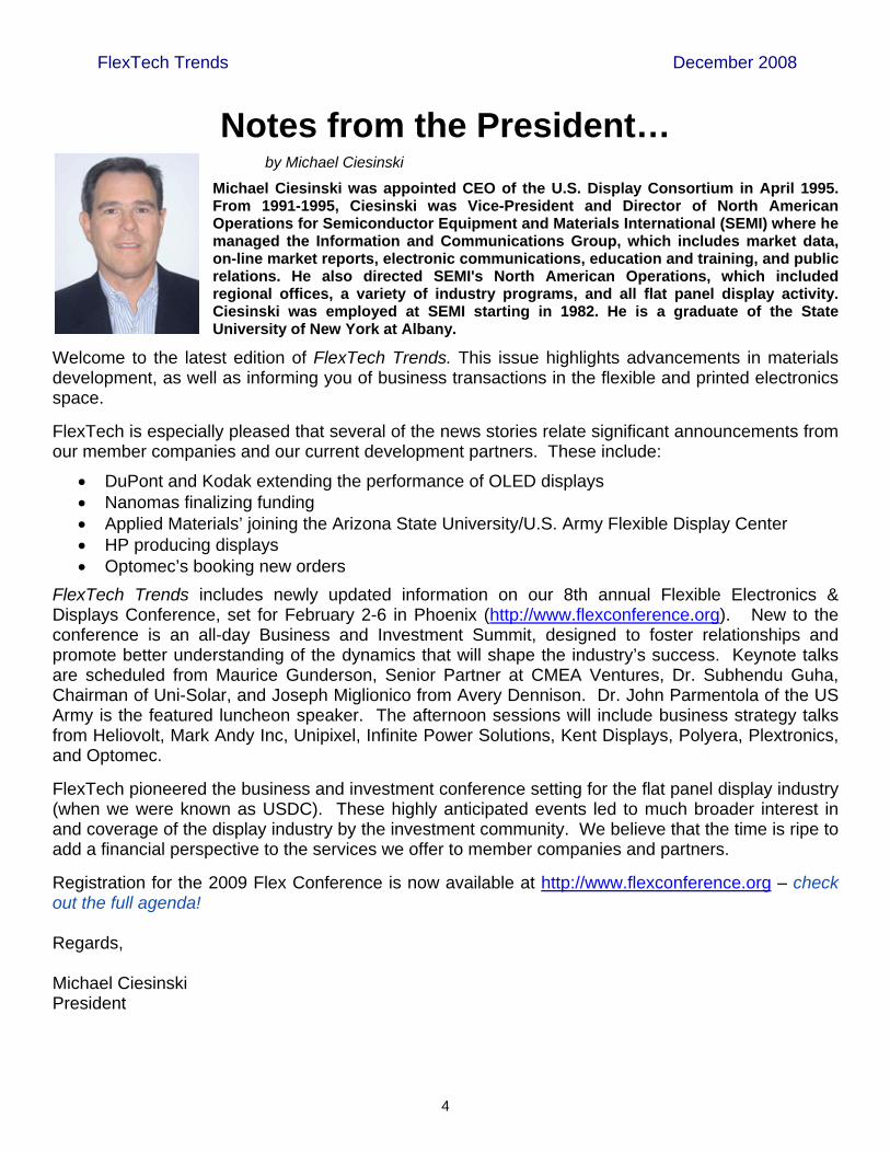
Michael Ciesinski was appointed CEO of the U.S. Display Consortium in April 1995. From 1991-1995, Ciesinski was Vice-President and Director of North American Operations for Semiconductor Equipment and Materials International (SEMI) where he managed the Information and Communications Group, which includes market data, on-line market reports, electronic communications, education and training, and public relations. He also directed SEMI's North American Operations, which included regional offices, a variety of industry programs, and all flat panel display activity. Ciesinski was employed at SEMI starting in 1982. He is a graduate of the State University of New York at Albany.
Welcome to the latest edition of FlexTech Trends. This issue highlights advancements in materials development, as well as informing you of business transactions in the flexible and printed electronics space.
FlexTech is especially pleased that several of the news stories relate significant announcements from our member companies and our current development partners. These include:
DuPont and Kodak extending the performance of OLED displays Nanomas finalizing funding Applied Materials’ joining the Arizona State University/U.S. Army Flexible Display Center HP producing displays Optomec’s booking new orders
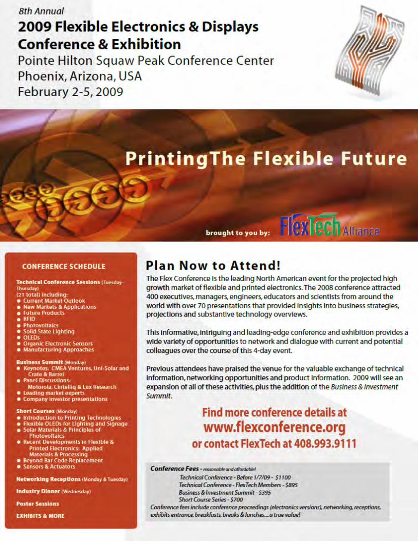
FlexTech Trends includes newly updated information on our 8th annual Flexible Electronics & Displays Conference, set for February 2-6 in Phoenix (http://www.flexconference.org). New to the conference is an all-day Business and Investment Summit, designed to foster relationships and promote better understanding of the dynamics that will shape the industry’s success. Keynote talks are scheduled from Maurice Gunderson, Senior Partner at CMEA Ventures, Dr. Subhendu Guha, Chairman of Uni-Solar, and Joseph Miglionico from Avery Dennison. Dr. John Parmentola of the US Army is the featured luncheon speaker. The afternoon sessions will include business strategy talks from Heliovolt, Mark Andy Inc, Unipixel, Infinite Power Solutions, Kent Displays, Polyera, Plextronics, and Optomec.
FlexTech pioneered the business and investment conference setting for the flat panel display industry (when we were known as USDC). These highly anticipated events led to much broader interest in and coverage of the display industry by the investment community. We believe that the time is ripe to add a financial perspective to the services we offer to member companies and partners.
Registration for the 2009 Flex Conference is now available at http://www.flexconference.org – check out the full agenda! Regards, Michael Ciesinski President

FlexTech Trends December 2008
5
FlexTech Alliance adds new features to Conference
8th annual Flexible Electronics and Displays Conference
The 8th annual Flexible Electronics and Displays Conference will be held February 2-6, 2009 in Phoenix, Arizona. Kicking off the three-day technical conference, Dr. Mark Pinto, senior vice president at Applied Materials, will deliver the keynote address. Dr. Pinto is General Manager of Applied's Energy and Environmental Solutions group and the company's Chief Technology Officer. The event has several new features which provides additional value and which is expected to draw additional attendance:
"Bridging the Information Gap" is the theme of the all-new Business and Investment Summit, scheduled for Monday, February 2nd. The summit will connect innovators and manufacturers of flexible, printed electronics and displays with investors and consumer product developers. Keynote talks include CMEA Ventures and Uni-Solar; along with feature a panel on "Where's the Beef? -- Real Opportunities in Flexible, Printed Electronics," which will showcase discussions by Motorola, cintelliq and Lux Research. Afternoon sessions will include business strategy talks from Infinite Power Solutions, Plextronics, Unipixel and Heliovolt.
By popular demand, the Monday short course has been expanded to a full day Short Course Series with six offerings. Attendees can mix and match morning and afternoon sessions. The courses cover topics in printing technologies, flexible and printed electronics, flexible OLEDs, solar and photovoltaic applications, RFIDs and sensor technology. Instructors include representatives from Alien Technology, Clemson University, Cornell University, Holst Centre, Merck and North Dakota State University.
One of the key goals of the 2009 Flex Conference is to disseminate the most current information on new and developing technologies in flexible, printed electronics and displays. As such, the addition of a new Late Breaking Results Poster Track is an opportunity for industry, academia and R&D institutions to present their work over all three days of the conference in an expanded venue. Plus, current data can be submitted as late as January 5th, to accommodate the most up-to-date developments.
Another all-new event is the FLEXI Awards. The FlexTech Industry Awards 2009, sponsored by the FlexTech Alliance, are open to all organizations in the flexible, printed electronics, and displays industries. Three awards will be given out at a premier dinner during the Flex Conference, on Wednesday, February 4th. The award categories are: “Research and Development”, “Most Innovative Product”, and Technology Leadership in Education”. Nominations for the FlexTech Industry Awards 2009 must be submitted via e-mail to [email protected] no later than January 9. Details can be downloaded here: http://www.flextech.org/documents/FLEXI_Cat.doc
For more information, or to register for the 8th annual Flexible Electronics and Displays Conference, visit http://www.flexconference.org. Sponsorship packages are still available.

FlexTech Trends December 2008
6
News from the FlexTech Alliance
excerpted from Veritas et Visus newsletters
Centre for Organic Photonics and Electronics opens in Australia The Centre for Organic Photonics and Electronics recently opened at the University of Queensland. The Centre is a joint initiative between the School of Molecular & Microbial Sciences and the School of Physical Sciences (Physics Discipline) includes integrated programs in experimental and theoretical condensed matter physics as well as synthetic chemistry, and is affiliated with the Faculty of Biological and Chemical Sciences and the Faculty of Engineering, Physical Sciences and Architecture at the University of Queensland. Condensed Matter research will be significantly enhanced by the University creating a new Centre for Organic Photonics and Electronics, based in the Chemistry building, within the School of Molecular and Microbial Sciences. This initiative is a result of the award of an Australian Research Council Federation Fellowship to Professor Paul Burn. The ceremony was held on the Podium of the Chemistry building, attended by senior members of UQ's executive, as well as State Government delegates, guest speakers and academic and research staff from several Australian universities. http://www.physics.uq.edu.au/cope/index.html
From left to right: Dr Shih-Chun Lo, Prof David Siddle, Dr Ben Powell, Prof Paul Burn, Prof Ross McKenzie, Prof Paul Greenfield, Prof Andrew Holmes and Assoc Prof Paul Meredith
Hodogaya promotes its transport materials for the Novaled PIN OLED structures Hodogaya Chemical Co. and Novaled, have agreed to offer hole transport materials for Novaled PIN OLED structures. Hodogaya has exclusively developed specific hole transport materials for Novaled fitting very well with the Novaled PIN OLED structures. As a first result Novaled is enhancing its material offer with an additional hole transport material called NHT18. The new NHT18 has a similar behavior in OLEDs like NPB, but provides additional advantages to OLED manufacturers. For example, the Tg of NHT18 is above 130°C and thus gives a high temperature stability in OLED devices. The current efficiency in today’s fluorescent blue emitting PIN OLEDs is 10% higher. http://www.hodogaya.co.jp http://www.novaled.com
Soligie and Blue Spark collaborate to develop market applications for printed flexible batteries Soligie and Blue Spark Technologies announced that they have entered into an agreement for the joint market development of Blue Spark's thin battery technology and Soligie's printed electronics capabilities. The companies anticipate that this agreement will lead to a manufacturing collaboration for roll-to-roll volume production of Blue Spark batteries. Printed electronics are increasingly utilized in product innovations including interactive product labels with iconic displays, smart medical patches, functional electronic devices, sensors, and radio frequency (RF)-enabled tags. http://www.soligie.com http://www.bluesparktechnologies.com

FlexTech Trends December 2008
7
OASYS selected for US Army’s Thermal Weapon Sight Remote Viewer Program OASYS Technology, an electro-optical solutions provider, and eMagin Corporation announced that OASYS has been selected by the United States Army to provide 20,000 units of the Remote Eyepiece Display-Imager (RED-I) head mounted display system for the Thermal Weapon Sight (TWS) Remote Viewer program. The RED-I system is equipped with eMagin OLED-XL microdisplays. The IDIQ contract awarded to OASYS exceeds $26 million with multi-year production rate deliveries scheduled to begin in the second quarter of 2009. The new RED-I product features instant-on startup at temperatures down to –40 deg C, extended battery life, and is compatible with both new and legacy TWS systems. The HMD attaches directly to standard-issue military helmets or protective eyewear, is thin enough to fit behind the blast visor of the cupola protective ensemble, and is backwards compatible with previous versions of the system. The thermal weapon sights are used with a variety of weapons to provide identification of targets as well as to see through smoke and fog. http://www.oasys-technology.com http://www.emagin.com
Applied Materials joins Flexible Display Center at Arizona State University The Flexible Display Center (FDC) at Arizona State University announced that Applied Materials, Inc., through its Display Business Group AKT, has become an Associate Member, joining the ranks of other world-class providers of technology, materials and process equipment who are collaborating with the FDC to develop advanced flexible electronic displays. Headquartered in Santa Clara, California, Applied is a leading supplier of systems, processes and services to the flat panel display manufacturing industry, focusing on applications that serve the TFT-LCD market. http://www.appliedmaterials.com http://www.flexdisplay.asu.edu
Signet Solar begins customer shipments of solar PV panels Signet Solar, a global manufacturer of thin film silicon photovoltaic (PV) modules, announced the production and shipment of the first megawatt of panels from its manufacturing facility in Mochau, Germany. The shipment comes only a month after Signet became the first licensee of Applied Materials’ SunFab production line to start high volume manufacturing ramp of the large-area thin film modules. Initial customer shipments are being delivered to Hanover-based alfasolar Vertriebsgesellschaft. In addition to alfasolar, Signet customers include several major photovoltaic system integrators such as Phönix Solar, Soleg, Goldbeck Solar, and SolarMarkt. Signet’s Mochau facility is now qualified for full production capacity of 20MW per year. In order to meet existing customer commitments of over $400 million, Signet has plans to expand its installed production capacity up to 130MW by the end of 2009. http://www.signetsolar.com
HP unveils flexible displays fabricated by the SAIL process Researchers have created flexible displays by using the self-aligned imprint lithography (SAIL) technology, invented by HP Labs, which enables the fabrication of thin film transistor (TFT) arrays on flexible plastic in what HP claims is a low cost and “roll to roll” manufacturing process. Potential uses for the new flexible displays, according to HP and the Flexible Display Center (FDC), are in electronic paper and future electronic devices that could use the extra battery life, such as smart phones and notebook computers. SAIL allows thin film transistors to be fabricated onto a flexible plastic material. This is then manufactured in a roll-to-roll process unlike the current sheet-to-sheet process for manufacturing displays. According to the Palo Alto, California-based company, the self-assembly process that patterns the thin film substrate material has been developed without using traditional lithography. The process is immune to minor distortions caused by variations in manufacturing, which are mainly due to its natural self-aligned nature. HP and the (FDC) at Arizona State University have developed the first prototype of low cost, flexible electronic displays that could be used for electronic paper and signage. The affordable solution is capable of rendering a full motion video, while its manufacturing process allows it to provide something that is called “sticky pixels”, which basically enables the pixels of the device to retain their state after the voltage has been removed. http://www.hpl.hp.com
Rockwell Collins completes SEOS acquisition Rockwell Collins completed its acquisition of SEOS, a leading global supplier of highly realistic visual display solutions for commercial and military full flight simulators. SEOS will operate under the Rockwell Collins name and will become part of the Simulation and Training Solutions organization. The acquisition is projected to be slightly accretive to Rockwell Collins' fiscal year 2009 earnings. Terms of the agreement were not disclosed. http://www.rockwellcollins.com

FlexTech Trends December 2008
8
DisplaySearch reports worldwide OLED revenues up 60% Y/Y in Q3’08 In its latest Q4’08 Quarterly OLED Shipment and Forecast Report, DisplaySearch reported that the worldwide OLED display revenue in Q308 was $141 million, down 11% Q/Q but up 60% Y/Y. Chi Mei EL, the #2 supplier of AMOLED displays, posted record high shipments in Q3’08, while the leading AMOLED supplier Samsung SDI, which will merge with Samsung Electronics’ small/medium business to form Samsung Mobile Display in January, experienced lower shipments Q/Q. As a result, AMOLED shipments increased only slightly compared to Q2’08, reaching 1.7 million units. After a strong Q2, PMOLED shipments were affected by reductions in mobile phone sub-display orders, so shipments fell 22% Q/Q. However, most of the shipment reduction was in monochrome PMOLED, while area color and full color PMOLED gained popularity. This led to an increase in average selling price for OLEDs in Q3’08. RiTDisplay passed Samsung SDI to take the lead in total OLED shipments with 36% market share. Samsung SDI is #2 in shipments, but still the leader in total OLED revenues thanks to its AMOLED shipments. TDK passed Pioneer to become #3 in shipments at 17%, while Pioneer fell to the #4 position at 12%; Univision was #5. The top five suppliers accounted for over 95% of total OLED shipments in Q3’08, as shown in the following table. Given the challenging economic climate and pressure from LCDs, DisplaySearch has revised its total OLED forecast for 2008 to 2015 downward from the previous forecast. However, there are new AMOLED applications, and several categories will gain momentum in 2009 and beyond. http://www.displaysearch.com
CDT and Semprius announce agreement to develop new OLED backplane technology Semprius announced that it has entered a joint development agreement with Cambridge Display Technology (CDT) to develop new technology for the manufacture of OLED backplanes for flat panel displays. The goal of the two-year collaboration is to apply Semprius’ patented semiconductor printing technology to improve performance of backplanes, which hold the electronic components that drive display screens for computers, televisions and a host of other devices. CDT, a wholly- owned subsidiary of Sumitomo Chemical, is a leader in the research and commercialization of polymer OLEDs and their application in displays. Semprius’ micro-transfer printing process allows transfer printing of high-performance semiconductors onto virtually any surface, including glass, flexible and rigid plastic, metal and other semiconductor materials. Semprius will focus on using its patented process to transfer single crystal silicon semiconductors onto the backplane, thereby increasing overall display performance. http://www.cdtltd.co.uk http://www.semprius.com
DuPont Displays showcases OLED displays and direct bonding adhesive for LCDs DuPont Displays showcased the latest generation of its active-matrix OLED displays and DuPont Vertak DBA2000 direct bonding adhesive at FPD International in Yokohama, Japan, October 29-31. For OLED displays, DuPont Displays has developed solution printed OLED technology that is designed to lower AMOLED manufacturing costs. DuPont’s proprietary technology includes a set of solution-based OLED materials that can be printed and coated at high speed using an innovative process. Fabrication of AMOLED displays by solution process reduces material consumption and lowers equipment costs compared to incumbent vapor deposition processes. These advantages result in significant cost benefits over both LCD and the incumbent OLED technology. 4.3-inch WQVGA AMOLED prototype displays were exhibited. The prototypes were printed on Chi Mei backplanes using a Dainippon Screen nozzle printer. Also on the show floor were DuPont Vertak DBA2000 direct bonding adhesives for evaluation. Vertak DBA2000 is a reworkable direct bonding adhesive that increases display ruggedization and sunlight readability and is a next-generation adhesive based on the performance characteristics of Vertak DBA1000. The optically clear Vertak bonding adhesives combine the benefits of alternative adhesives like silicone and epoxy, and are highly resistant to yellowing, delamination and bubble formations. Now, Vertak DBA2000 adhesive enables the separation of LCD touch screens and other substrates from bonded cover plates within minutes, and then allows the components to be immediately rebonded. http://www.DuPont.com
Rank Supplier Q3�08 Market
Share 1 RiTDisplay 36% 2 Samsung SDI 26% 3 TDK 17% 4 Pioneer 12% 5 Univision 4.4%
Others 4.6% Total 100.0%
Top Five OLED Suppliers and Share in Q3’08

FlexTech Trends December 2008
9
Add-Vision awarded Core Technologies Grant by DOE for $1.56 million Add-Vision announced that it has been selected by the National Energy Technology Laboratory (NETL) for a three year research and development project entitled “Low Cost, High Efficiency Polymer OLEDs based on Stable p-i-n Device Architecture”. The research project represents a collaborative research between Add-Vision, Dr. Qibing Pei’s research team at the University of California, Los Angeles (UCLA), and Dr. Sue Carter’s research team at the University of California, Santa Cruz (UCSC). Under the project, the research teams will design and synthesize advanced materials to enable a next-generation polymer OLED technology, one that is high efficiency, long-lived, and manufacturable using low cost processing assuring adoption into solid state lighting (SSL) applications. NETL will fund up to $1.56 million of the $2.2 million research project, with yearly funding based on successful delivery of milestones. http://www.add-vision.com
Ohio State University orders AIXTRON system for solar cell development AIXTRON announced an order for a Close Coupled Showerhead (CCS) MOCVD reactor from the Ohio State University in Columbus, Ohio, USA, received in the third quarter 2008. The CCS tool in the 3x2-inch wafer configuration is planned to be delivered to the Ohio State University Institute for Materials Research (IMR) and the Wright Center for Photovoltaics Innovation and Commercialization (PVIC), a state funded center to promote research collaboration and commercialization in photovoltaics. http://www.aixtron.com
New Kodak material boosts OLED performance and energy efficiency Eastman Kodak announced the introduction of a highly efficient OLED material that will enable low-power, full-color displays with outstanding lifetimes. The new material, trademarked Kodak OLED Material EK-GD403, utilizes green dopant technology to deliver a new level of OLED display performance and reliability. Green dopants are materials that control color output and boost efficiency. OLED Material EK-GD403, used in combination with Kodak OLED Material EK-BH109, provides low-voltage green OLEDs with luminous efficiencies greater than 31cd/A and lifetimes in excess of 65,000 hours (from an initial luminance of 1,000cd/m2) and results in an external quantum efficiency of 8.7%. http://www.kodak.com/go/displays
Department of Defense awards Endicott Interconnect Technologies $12M R&D contract Endicott Interconnect Technologies (EI) announced that it has been awarded a $12 million R&D contract by the US Department of Defense to continue development of electronic packaging technologies including printed circuit boards and organic substrates for a super computer application. This contract supports the exploration and development of advanced high-speed electronic packaging technologies; specifically, system development, printed circuit board and substrate design along with the evaluation of alternative material sets. Existing facilities have been expanded and modified to accommodate new equipment, which has been purchased to support this work and EI anticipates additional hiring needs. http://www.endicottinterconnect.com
Orbotech completes acquisition of Photon Dynamics Orbotech announced that it has successfully consummated the acquisition of Photon Dynamics, a provider of test and repair systems for the LCD FPD industry. Under the terms of the agreement, Orbotech is paying $15.60 per share in cash for all of the issued and outstanding shares of Photon Dynamics’ common stock, resulting in an aggregate purchase price of approximately $290 million. The acquisition was financed through a combination of internally-generated funds and external-source financing. This transaction will be immediately accretive to Orbotech on a cash basis, and the company expects, as a result of its completion, to record additional FPD revenues of approximately $45-50 million during the remainder of 2008. However, particularly given the prevailing, considerable worldwide economic uncertainty and its potential effect on the electronics industry, the company is currently unable to estimate reliably revenues in subsequent quarters. While the combined level of backlog in FPD systems for the company and Photon Dynamics is at an all-time high and Orbotech believes that it will remain firm, the company recognizes the potential for materially adverse trends in future orders, including deferrals. In addition, as a result of this acquisition, Orbotech expects to realize operational synergies of approximately $15-20 million in 2009. http://www.orbotech.com
FlexTech Trends December 2008
10
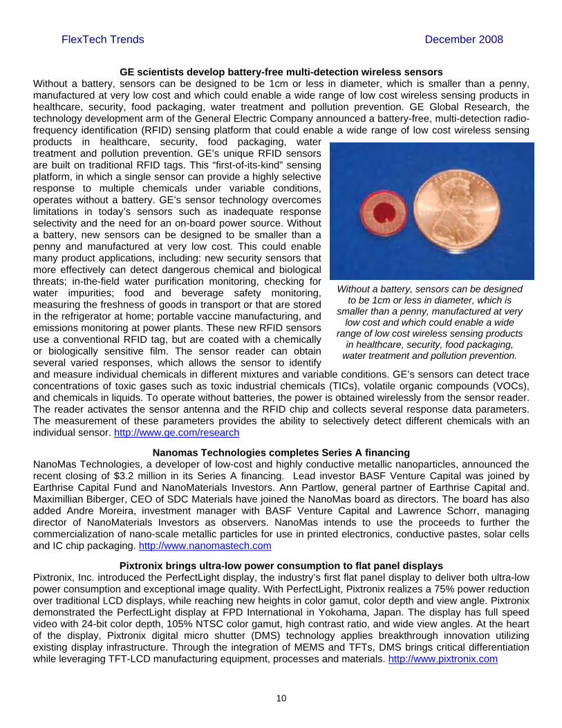
GE scientists develop battery-free multi-detection wireless sensors Without a battery, sensors can be designed to be 1cm or less in diameter, which is smaller than a penny, manufactured at very low cost and which could enable a wide range of low cost wireless sensing products in healthcare, security, food packaging, water treatment and pollution prevention. GE Global Research, the technology development arm of the General Electric Company announced a battery-free, multi-detection radio-frequency identification (RFID) sensing platform that could enable a wide range of low cost wireless sensing products in healthcare, security, food packaging, water treatment and pollution prevention. GE’s unique RFID sensors are built on traditional RFID tags. This “first-of-its-kind” sensing platform, in which a single sensor can provide a highly selective response to multiple chemicals under variable conditions, operates without a battery. GE’s sensor technology overcomes limitations in today’s sensors such as inadequate response selectivity and the need for an on-board power source. Without a battery, new sensors can be designed to be smaller than a penny and manufactured at very low cost. This could enable many product applications, including: new security sensors that more effectively can detect dangerous chemical and biological threats; in-the-field water purification monitoring, checking for water impurities; food and beverage safety monitoring, measuring the freshness of goods in transport or that are stored in the refrigerator at home; portable vaccine manufacturing, and emissions monitoring at power plants. These new RFID sensors use a conventional RFID tag, but are coated with a chemically or biologically sensitive film. The sensor reader can obtain several varied responses, which allows the sensor to identify and measure individual chemicals in different mixtures and variable conditions. GE’s sensors can detect trace concentrations of toxic gases such as toxic industrial chemicals (TICs), volatile organic compounds (VOCs), and chemicals in liquids. To operate without batteries, the power is obtained wirelessly from the sensor reader. The reader activates the sensor antenna and the RFID chip and collects several response data parameters. The measurement of these parameters provides the ability to selectively detect different chemicals with an individual sensor. http://www.ge.com/research
Nanomas Technologies completes Series A financing NanoMas Technologies, a developer of low-cost and highly conductive metallic nanoparticles, announced the recent closing of $3.2 million in its Series A financing. Lead investor BASF Venture Capital was joined by Earthrise Capital Fund and NanoMaterials Investors. Ann Partlow, general partner of Earthrise Capital and. Maximillian Biberger, CEO of SDC Materials have joined the NanoMas board as directors. The board has also added Andre Moreira, investment manager with BASF Venture Capital and Lawrence Schorr, managing director of NanoMaterials Investors as observers. NanoMas intends to use the proceeds to further the commercialization of nano-scale metallic particles for use in printed electronics, conductive pastes, solar cells and IC chip packaging. http://www.nanomastech.com
Pixtronix brings ultra-low power consumption to flat panel displays Pixtronix, Inc. introduced the PerfectLight display, the industry’s first flat panel display to deliver both ultra-low power consumption and exceptional image quality. With PerfectLight, Pixtronix realizes a 75% power reduction over traditional LCD displays, while reaching new heights in color gamut, color depth and view angle. Pixtronix demonstrated the PerfectLight display at FPD International in Yokohama, Japan. The display has full speed video with 24-bit color depth, 105% NTSC color gamut, high contrast ratio, and wide view angles. At the heart of the display, Pixtronix digital micro shutter (DMS) technology applies breakthrough innovation utilizing existing display infrastructure. Through the integration of MEMS and TFTs, DMS brings critical differentiation while leveraging TFT-LCD manufacturing equipment, processes and materials. http://www.pixtronix.com
Without a battery, sensors can be designed to be 1cm or less in diameter, which is
smaller than a penny, manufactured at very low cost and which could enable a wide
range of low cost wireless sensing products in healthcare, security, food packaging,
water treatment and pollution prevention.

FlexTech Trends December 2008
11
NanoGram Corporation and Tokyo Electron enter thin-film photovoltaics JDA NanoGram Corporation, a developer and manufacturer of products and solutions for optical, electronic and energy applications, announced that it has extended its relationship with Tokyo Electron Ltd. from strategic investor to technology and market development partner by entering into a joint development agreement. The JDA will focus on developing advanced thin film deposition tools based on NanoGram’s patented laser reactive deposition (LRD) process for silicon. The platform will be targeted for the rapidly growing thin film photovoltaics market, which is expected to grow to 40% of the entire PV market by 2012 according to the Prometheus Institute. NanoGram’s LRD process has a distinct rate advantage with the capability to deposit amorphous and microcrystalline silicon significantly faster than conventional CVD processes. The development work is also expected to be complementary to NanoGram’s breakthrough low-cost multi-crystalline SilFoil PV module business. This announcement comes on the heels of NanoGram’s receipt of the Energy Innovator Award from the US Department of Energy’s Office of Energy Efficiency and Renewable Energy for its SilFoil multi-crystalline photovoltaic product. The company is planning five megawatts of capacity to be on line by end of 2009. http://www.nanogram.com http://www.tel.com
ESI and Zygo announce agreement to merge Electro Scientific Industries and Zygo Corporation announced that they have entered into a definitive agreement under which the companies will merge in an all stock transaction. This merger combines two photonics-based technology leaders, possessing complementary technologies and strong brand names: ESI is a leading provider of world-class photonic micro-engineering solutions, while Zygo is a leader in the field of high-precision metrology solutions and optical systems. Revenues for the combined company for calendar year 2007 were approximately $458 million. http://www.zygo.com http://www.esi.com
NIST clarifies electrical and optical behavior of nanotubes Using highly uniform samples of carbon nanotubes – sorted by centrifuge for length – materials scientists at the National Institute of Standards and Technology (NIST) have made some of the most precise measurements yet of the concentrations at which delicate mats of nanotubes become transparent, conducting sheets. Their recent experiments point up the importance of using relatively homogeneous – not overly short, but uniform in length – nanotubes for making high performance conducting films. Relatively small concentrations of nanotubes can change a normally insulating polymer film to a transparent electrical conductor. Potential applications range from transparent electrical shielding materials to futuristic flexible video displays, thin-film chemical sensors and other foldable electronics. One key design parameter for conductive films is the so-called “percolation threshold” – essentially the concentration at which random two or three-dimensional networks of nanotubes first become electrically conducting.
To test theories on how both the conductance and optical properties of such nanotube-infused films depend on the length of the tubes, the NIST team made samples of “buckypaper” by mixing nanotubes in water and draining the water away through nanoscale filters to leave behind a delicate nanotube mat. The highly refined, length-sorted nanotube samples were produced by an efficient technique developed earlier by the NIST group. The NIST measurements validated one theory: buckypaper made of length-sorted carbon nanotubes closely follows the percolation theory for ideal two-dimensional sheets, with concentration threshold for conductivity getting lower as the tubes get longer. A sheet of 820 nanometer long nanotubes becomes conducting at an amazingly low 18 nanograms per square centimeter, the lowest yet reported. http://www.nist.gov
Buckypaper: SEM image demonstrates a pseudo 2D network of carbon nanotubes deposited like paper fibers in a thin, sparse sheet.
The nanotubes here have an average length 820nm and make a continuous, electrically conducting network overall in spite of obvious
gaps. On a macroscale this material would be nearly transparent. Color
added for clarity.

FlexTech Trends December 2008
12
NIST develops better organic semiconductors for printable electronics Researchers from the National Institute of Standards and Technology (NIST) and Seoul National University (SNU) have learned how to tweak a new class of polymer-based semiconductors to better control the location and alignment of the components of the blend. Their recent results – how to move the top to the bottom – could enable the design of practical, large-scale manufacturing techniques for a wide range of printable, flexible electronic displays and other devices. Small organic molecules have been developed with key electrical parameters close to the benchmark set by amorphous silicon semiconductors, but they are very difficult to deposit in a stable, uniform film – a key manufacturing requirement. Larger molecule polymer semiconductors, on the other hand, make excellent thin films but have at best limited semiconductor properties. A patent from British researchers in 2005 offered a promising compromise: blend the small semiconductor molecules in with the polymer. Tests showed that actual devices, field effect transistors, made with the blend only worked well in a so-called “top-gated” structure. The critical active part of the film was on the top, and the switching part of the device (the “gate”) had to be layered on top of that, a process difficult or impossible to do on a large scale without destroying the fragile film.
Working at NIST’s Center for Neutron Research, the SNU/NIST research team used a neutron imaging technique that allowed them to observe, with nanometer resolution, how the distribution of small organic semiconductor molecules embedded in polymer films changed with depth – the films are less than 100 nanometers thick. In the thin films originally described by the patent, the bulk of the semiconductor molecules end up at the top of the film, as suspected. However, when the SNU/NIST research team substituted a polymer with significantly higher molecular mass, something interesting happened. The organic semiconductor small molecules distributed themselves evenly at the top and bottom of the film. Having an active region of the film on the bottom is key for large-scale manufacturing because it means the rest of the device – gate, source, drain – can be laid down first and the delicate film layer added last. In addition, they report, the optimized blend of polymer and organic semiconductor actually has better performance characteristics than the organic semiconductor on its own. http://www.nist.gov
SFC and Universal Display Corporation enter into strategic business agreement Universal Display Corporation and SFC, a Korean manufacturer of OLED materials, announced that the companies have entered into a strategic business agreement to develop and commercialize highly-efficient phosphorescent OLED material systems. Based on Universal Display’s proprietary PHOLED technology, Universal Display will support SFC’s development and marketing of phosphorescent hosts and other non-emitter materials that are matched to Universal Display’s phosphorescent OLED emitter materials. The companies will market and sell their respective materials that result from the SFC collaboration. As part of the arrangement, SFC will transfer certain existing phosphorescent emitter materials to Universal Display, including manufacturing and sales of these materials. http://www.universaldisplay.com http://www.sfc-dye.com
Plextronics awarded $1.2 million in government funding for flexible printed electronics Plextronics, a technology company that specializes in printed solar, lighting and other electronics, announced that it has secured $1.2 million in funding as part of the 2009 Defense Appropriations Bill Continuing Resolution (H.R. 2638) that was signed into law on September 30. The award is a new contract for the company to develop flexible and light-weight printed electronics for the United States military, including products and applications such as flexible solar panels for tent tops, solar-powered foldable blankets and helmet-mounted panels, printed lighting, flexible displays and printed circuitry. http://www.plextronics.com
Restacking organic semiconductors: an improved formulation for a polymer blend semiconductor causes key semiconducting
molecules to migrate to the bottom of the active layer, allowing chip designers to replace top-gated structures (a) with more easily
manufactured bottom-gate, bottom-contact devices (b).

FlexTech Trends December 2008
13
IMEC and Plextronics collaborate on high-efficiency reproducible organic solar cells IMEC, Europe’s leading independent nanoelectronics research institute and Plextronics signed an agreement to collaborate on state-of-the-art materials and inks for organic solar cells. With this collaboration, IMEC aims to develop a reproducible process for high-efficiency organic solar cells using Plextronics’ Plexcore branded materials and inks, which have demonstrated world-record efficiencies as high as 5.9%, according to recent testing at the National Renewable Energy Laboratory (NREL) in Colorado. IMEC aims to develop organic multi-junction solar cells with efficiency of 10% by 2012. The company’s focus is also on up-scaling of the process to achieve a large-area industrial manufacturing technology with an average efficiency of 7% (+/- 0.5%) and solar cell lifetime of five years. To realize these goals, high-quality, highly reproducible commercial materials are essential. In the first phase, IMEC will investigate Plexcore OS, which is a regio-regular poly-3-hexylthiophene (P3HT) polymer with a high absorption coefficient close to the maximum photon flux in the solar spectrum and high mobility. Plexcore OS materials will be processed using spin coating and validated on film morphology, carrier mobility and reproducibility. Solar cells will be processed on different substrates using spin-coated films of the material. Future research will include evaluation of other Plexcore materials and inks, using deposition techniques such as screen and inkjet printing and spray coating on large-area substrates. http://www.imec.be http://www.plextronics.com
Nano-C awarded fundamental patents for carbon nanotube and fullerene manufacturing
Nano-C, a developer of nanostructured carbon materials, announced that it has been issued US Patent Nos. 7,335,344 and 7,396,520 by the Department of Commerce’s United States Patent and Trademark Office. These newly issued patents cover the manufacture of Nano-C’s core products, carbon nanotubes and fullerenes. “The fundamental competitive advantage of our technology covered by these patents enables us to offer an array of unique carbon nanotubes and fullerene products, tailored to specific applications,” commented Viktor Vejins, president and CEO at Nano-C. “These technologies provide the needed scalability to meet the growing demands we see in organic photovoltaic (OPV) and electronics applications, including transparent conducting films for use in a variety of display, touch-screen and traditional solar applications.” http://www.nano-c.com
Sencera demonstrates 7% efficient thin-film silicon solar cells Sencera, a developer of photovoltaic modules and thin film solar panel systems, has successfully deposited single-junction silicon solar cells with 7% sunlight to electricity conversion efficiencies under standard test conditions. The company achieved the result utilizing a repeatable, fully automated process on the Viper, its proprietary plasma enhanced chemical vapor deposition (PECVD) manufacturing platform. Cell performance was independently measured and confirmed by the University of Delaware’s Institute of Energy Conversion, designated a University Center of Excellence for Photovoltaic Research and Education by the Department of Energy and The National Renewable Energy Laboratory (NREL). Sencera’s 7% conversion efficiency milestone triggered an additional $5.2 million equity investment by The Quercus Trust and Michael Draper of Equinox Securities, Sencera’s largest investor. According to Britt Weaver, Sencera’s CFO, “Proceeds will be utilized to further accelerate the development of second generation tandem amorphous/microcrystalline solar cells with expected conversion efficiencies greater than 10%. Sencera is also in the process of raising additional capital in order to fully fund its first 35-megawatt module factory in Charlotte, North Carolina.” http://www.sencera.com
Optomec reports new orders for aerosol jet solar lab printing system Optomec announced that the company has received significant orders for its aerosol jet solar lab system since its introduction earlier this year. The solar lab system is a process development platform that enables customers to define and develop improved collector line patterns for current and next generation high-efficiency solar cells by printing much finer collector lines than is currently possible with traditional screen-printing methods. These narrower, high integrity collector lines have higher conductivity and a lower shadowing effect, thereby increasing photovoltaic cell efficiency (>1%). Additionally, the non-contact deposition process used by aerosol jet is ideal for printing on thinner wafers. The system is commonly used as a precursor before moving to a full production aerosol jet print line solution provided in partnership with Manz Automation. http://www.optomec.com
FlexTech Trends December 2008
14
Fraunhofer ISE produces solar cells exceeding 20% efficiency printed by Optomec The Fraunhofer Institute for Solar Energy Systems (ISE) has continued progress in producing high efficiency solar cells using aerosol jet printing equipment developed by Optomec. The aerosol jet printed solar cells achieved efficiencies of over 20% when combined with light induced plating (LIP) and annealing, versus an average efficiency for screen-printed mono-crystalline front junction silicon solar cells in the range of 16–18%. Because the process is non-contact, Optomec’s aerosol jet system can print on thinner wafers and with less breakage than screen-printing. The Fraunhofer study states:
“So far, the front side metallization holds the main potential for a further increase in cell efficiency. The main targets are the reduction of the metalized area to reduce shading losses, a low contact resistivity to a lowly doped emitter, and a high line conductivity to transport the current as loss-free as possible out of the cell. The cells fabricated in this work combine the advantages of a new advanced front side metallization with an already established rear contact process, which are both industrially feasible. The front side grid was aerosol jet printed and light induced plated achieving line widths below 45 micron. On solar cells with an 110V/sq emitter record cell efficiencies of 20.3% were measured. In fact in a recent work, Fraunhofer ISE has found that the optical width of an aerosol jet printed and plated contact embedded in a module is only 43% of its geometrical width further reducing fill factor and providing increased cell/module efficiencies.”
For volume production applications, Optomec has developed a high throughput 40-nozzle aerosol jet deposition head that prints a solar cell every 2.5 to 3 seconds. Additionally, the non-contact nature of the aerosol jet system enables high yield printing on thinner photovoltaic wafers. http://www.ise.fhg.de
FlexTech Alliance awards contract to Akron Polymer Systems to develop flexible optical substrates The FlexTech Alliance awarded a contract to Akron Polymer Systems (APS) to develop transparent polymer films for flexible display technologies. The goal of this project is to develop polymer materials that can potentially replace the glass substrates now used in LCDs, as well as other display technologies. In order to successfully replace glass, a polymer that can deliver optical, thermal, chemical, and mechanical properties is necessary. “We are pleased be part of the technology that will enable the military to have flexible, lightweight and rugged information displays,” stated Dr. Frank Harris, APS’ chief operating officer. “There is also exciting commercial potential for these polymers in applications such as flexible solar cells and flexible electronics.” http://www.flextech.org http://www.akronpolysys.com
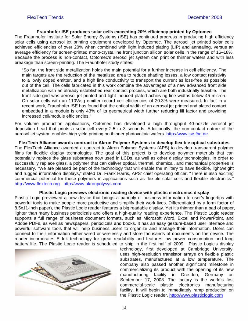
Plastic Logic previews electronic-reading device with plastic electronics display Plastic Logic previewed a new device that brings a panoply of business information to user’s fingertips with powerful tools to make people more productive and simplify their work lives. Differentiated by a form factor of 8.5x11-inch paper), the Plastic Logic reader features a big readable display. Yet it’s thinner than a pad of paper, lighter than many business periodicals and offers a high-quality reading experience. The Plastic Logic reader supports a full range of business document formats, such as Microsoft Word, Excel and PowerPoint, and Adobe PDFs, as well as newspapers, periodicals and books. It has an easy gesture-based user interface and powerful software tools that will help business users to organize and manage their information. Users can connect to their information either wired or wirelessly and store thousands of documents on the device. The reader incorporates E Ink technology for great readability and features low power consumption and long battery life. The Plastic Logic reader is scheduled to ship in the first half of 2009. Plastic Logic’s display
technology, first developed at Cambridge University, uses high-resolution transistor arrays on flexible plastic substrates, manufactured at a low temperature. The company also passed another significant milestone in commercializing its product with the opening of its new manufacturing facility in Dresden, Germany on September 17, 2008. The factory is the world’s first commercial-scale plastic electronics manufacturing facility. It will begin to immediately ramp production on the Plastic Logic reader. http://www.plasticlogic.com

FlexTech Trends December 2008
15
DuPont Microcircuit Materials launches new silver conductive ink for printed electronics DuPont Microcircuit Materials (MCM) announced the introduction of a new silver conductive ink formulated for use in printed electronics. DuPont 5064 silver conductive ink is a polymer thick film technology developed with a unique combination of silver powder and resin that provides superior conductivity, cost-effectively, it is claimed. It also allows for single pass printing, which improves productivity in a range of printing processes. Its adhesion to various substrates makes it suitable for several key applications, particularly RFID antennae, due to its performance in ultra high frequency and high frequency ranges. DuPont 5064 silver conductive ink may also be used for applications including membrane touch switches, biosensors, and interconnection circuitry. http://mcm.dupont.com
US Department of Energy investigates novel graphene applications Results of research at the Department of Energy’s Advanced Light Source (ALS), from DOE’s Lawrence Berkeley National Laboratory and the University of California at San Diego (UCSD) point to novel practical applications such as tunable optical modulators for communications and other nanoscale electronics. Graphene is the two-dimensional crystalline form of carbon: a single layer of carbon atoms arranged in hexagons, like a sheet of chicken wire with an atom at each nexus. The familiar pencil-lead form of carbon, graphite, consists of layers of carbon atoms tightly bonded in the plane but only loosely bonded between planes; because the layers move easily over one another, graphite is a good lubricant. These graphite layers are in fact graphene, although they had never been observed in isolation before 2004, at the University of Manchester. Once demonstrated, research immediately took off, inspired by the material's unexpected electronic properties. As a crystal, 2D graphene is quite dissimilar from 3D materials such as silicon, the Berkeley Lab said in a statement. “In semiconductors and other materials, charge carriers (electrons and oppositely charged ‘holes’) interact with the periodic field of the atomic lattice to form quasi-particles (excitations that act like actual particles). But quasi-particles in graphene do not look anything like an ordinary semiconductor’s. One interesting consequence of this unique band structure is that the electrons in graphene move ballistically – without collisions – over great distances, even at room temperature. As a result, the ability of the electrons in graphene to conduct electrical current is 10 to 100 times more than those in a normal semiconductor like silicon at room temperature. This makes graphene a very promising candidate for future electronic applications. http://www.lbl.gov
Flexible Display Center develops high temperature process for ultra-thin, rugged plastic displays The Flexible Display Center at Arizona State University developed a new process for manufacturing high-performance flexible displays on transparent plastic. FDC researchers, working with industrial partners DuPont Teijin Films and E Ink Corp., have developed a method for making high-performance amorphous silicon thin film transistors on planarized Teonex PEN films. The FDC team integrated 3.8-inch 320x240 pixel arrays of these transistors with Vizplex-100 imaging layer film from E Ink to fabricate glass-free high-performance flexible electrophoretic displays that are only 375 micrometers thick. The displays are quite rugged and readily withstand severe vibration and impact tests performed at industry partner General Dynamics’ labs. For video highlights of these tests go to http://flexdisplay.asu.edu/Flex-display-test_revB.wmv. The FDC thin film transistors are produced using the highest semiconductor and gate-dielectric deposition temperatures reported for a process on Teonex PEN. The higher temperatures permit the fabrication of transistors with higher on-off ratio, better sub-threshold slope, and – most importantly – greater bias-stress stability. These performance characteristics translate directly into higher pixel densities for enhanced display resolution and an enlarged number of gray levels.
Graphene is a two-dimensional crystal consisting of a single layer of carbon atoms arranged hexagonally. The energy bands of 2D graphene are smooth-sided cones, which
meet at the Dirac point.

FlexTech Trends December 2008
16
The FlexTech 2009 Open Solicitation
The FlexTech Alliance’s mission is to develop and organize the U.S. manufacturing expertise to expand the infrastructure required to support world-class manufacturing capability for displays and flexible, printed electronics. The FlexTech Alliance will oversee and administer funds provided by the U.S. Government through the Army Research Laboratory (ARL) for this purpose.
The specific mission includes development of the manufacturing equipment, materials, components, and processes required for more cost-effective fabrication of current and next generation flexible electronics and display products. A special emphasis is on the developments necessary to enable displays to be fabricated on flexible substrates as part of the Army’s Flexible Display Initiative. An emphasis is also being placed on developments directed at enabling web-based (roll-to-roll) manufacturing of displays and other electronic components.
Projects selected on flexible display materials, process technology and batch processing tools will be evaluated and may be integrated into the work plan for the Army R&D Center for Flexible Displays, located at the Arizona State University, as a part of the Army Flexible Display Initiative. Projects related to development of roll-to-roll manufacturing tools will be evaluated and may be integrated into the prototype production facility of the Center for Advanced Microelectronics Manufacturing [CAMM], which is directed by the State University of New York at Binghamton, and located in the facilities of Endicott Interconnect Technologies.
Proposal Process: To achieve the objectives on supplier quality and insertion into manufacturing, FlexTech Alliance is actively seeking proposals for the design, development and delivery of new or substantially improved process technology and manufacturing equipment, materials and components supply used in the fabrication of electronic displays and printed flexible electronics. This is an open solicitation, such that detailed objectives and end point specifications/requirements for a specific manufacturing process or material have not been predefined.
Applicants may submit a proposal on any topic related to enhancement in capability and/or cost for display or flexible, printed electronics manufacturing as cited above. The section labeled “Priority Proposal Topics” provides a list of topics for which FlexTech Alliance member companies have expressed interest. This list is not all-inclusive, but is meant as a guide on topics viewed as priority needs for the industry by the FlexTech Alliance Technical Council members.
In soliciting these proposals, FlexTech Alliance plans to grant and administer funding which must be matched (50% minimum) with funds in the form of cash and in-kind contributions provided by the grant recipients to cover the total project cost. If all other criteria are equal, preference will be given to proposals with a higher percentage of cost share. It should be noted that historically, cost share for the funded development programs has averaged over 65% industry funding. Project Teams of skilled technical resources from the FlexTech Alliance consortium member companies will be identified to provide project oversight and direction, as well as support for the process integration and evaluation at one or more of the consortium members’ manufacturing facilities, the Army Flexible Displays Center at ASU, or the CAMM at Binghamton University. These Project Teams typically will be comprised of 2 to 4 experts from the consortium companies and members from the successful individual supplier or supplier team.

FlexTech Trends December 2008
17
Priority Proposal Topics: Pre-proposals and complete proposals will be accepted on all topics related to materials, equipment, and technology development for flexible, printed electronics and display manufacturing. As a guide, a selection of topics for which the FlexTech Alliance Technical Council members have expressed specific interest is listed below. Responses do not need to be restricted to topics on this list:
Priority topics in Materials: UV curable hybrid organic/inorganic dielectrics UV curable hybrid organic/inorganic conductive inks Flexible transparent conductive films Low T/High K gate dielectric materials & process Cost-effective, novel packaging for flexible displays/lighting/photovoltaics, including
atmospheric deposited barriers and edge adhesives/sealants Novel organic semiconductor materials and manufacturing processes Printable Anti-reflective coatings Materials registry for inks and printing processes Projection displays: LCOS inorganic alignment layers, optical films
Priority topics in Equipment: Web-based defect inspection tool & process for flexible electronics Mask-less lithography Non-contact cleaning processes and tools for flexible electronics Array testing of OLED backplanes Patterned conductor repair Device design and process workflow for printed electronics Barrier testing standards for comparison of materials/coatings
Priority topics in Technology Development: Electronic textiles Flexible touch screens and actuators Improved materials & process for chips on flex Medical applications for printed and flexible electronics Combined sensors and displays using printed electronics Novel applications of flexible and printed electronics for DoD and/or commercial applications
2009 RFP Schedule: The schedule of activities for the FlexTech Alliance 2009 RFP is as follows:
11/21/08 Solicitation of pre-proposals issued 01/16/09 Pre-Proposals Due 02/02/09 Selection for full proposals (notification within 1 week of selection) 03/13/09 Full Proposals Due 03/25/09 Final Selection by FlexTech Alliance Technical Council To August 2009 Presentation to FlexTech Alliance Governing Board for approval
To submit a complete proposal and to receive a grant from FlexTech, the company or companies must be supporting members of the FPD industry and FlexTech through a FlexTech Membership or as a member of one of the USDC User Groups. This requirement does not need to be met in order to submit the initial pre-proposal. However, if the pre-proposal generates interest and the submitter chooses, upon FlexTech request, to prepare and submit a complete proposal, then the requirement for membership must be met before the proposal can be evaluated and given consideration for funding.
Further details about submitting a proposal for the 2009 FlexTech Alliance Open Solicitation are available at: http://flextech.org/about/program-rfps.aspx

FlexTech Trends December 2008
18
Special Section
Flexible Electronics and Displays 2009
The 8th annual Flexible Electronics & Displays Conference 2009 is significantly expanded to include topics in the emerging field of flexible, printed and organic electronics including equipment for high-throughput manufacturing of electronic printing processes and technologies, flexible displays, photovoltaics, solid-state lighting and organic light-emitting diodes (OLEDs), radio-frequency identification (RFID), and smart sensors.
The Flex Conference will be held February 2-5, 2009 at the Pointe Hilton Squaw Peak Resort in Phoenix, Arizona. This conference has evolved to become the leading North American event for the projected high growth market of flexible and printed electronics. The 2008 conference attracted 400 executives, managers, engineers, educators and scientists from around the world with over 70 presentations that provided insights into business strategies, projections and substantive technology overviews. Another key reason for the growth of the Flex Conference is the variety of opportunities to network and dialogue with current and potential colleagues throughout the event.
In 2009, the conference will include four distinct tracks: 1) Business, Markets, Applied and Developmental Research; 2) Fundamental Research; 3) Late Breaking Results, an opportunity to present the most up-to-date results through posters; and 4) Student Research Posters, with a competition for best posters.
2009 Flexible Electronics & Displays Conference Overview page 19 Business & Investment Summit Agenda page 21 Short Course Series Agenda page 22 Preliminary Technical Conference Agenda page 23
FlexTech Trends December 2008
19

FlexTech Trends December 2008
20
FlexTech Trends December 2008
21
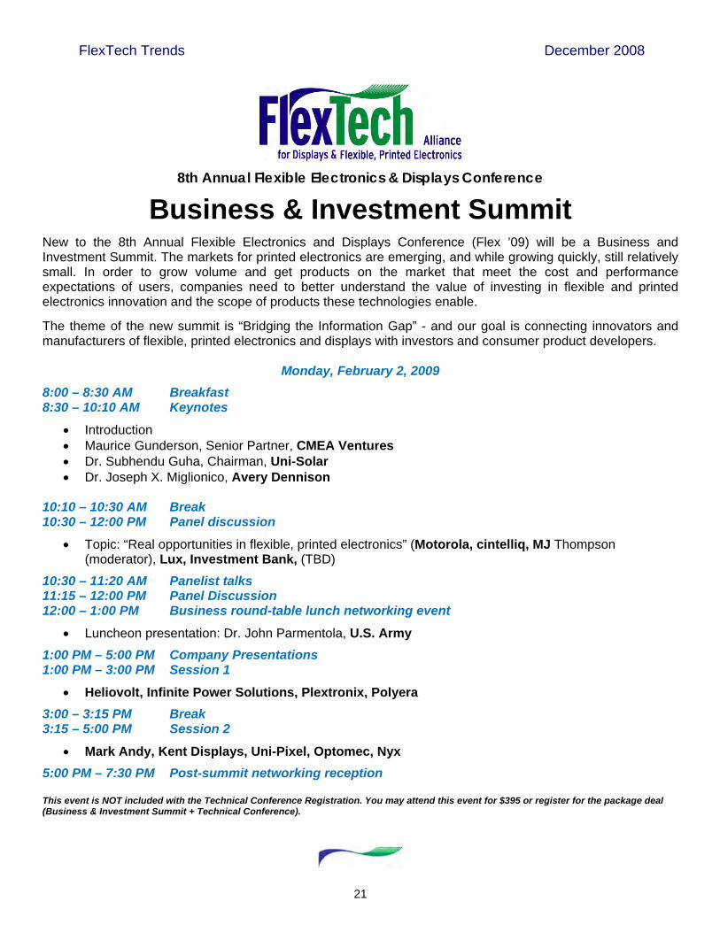
8th Annual Flexible Electronics & Displays Conference
Business & Investment Summit
New to the 8th Annual Flexible Electronics and Displays Conference (Flex ’09) will be a Business and Investment Summit. The markets for printed electronics are emerging, and while growing quickly, still relatively small. In order to grow volume and get products on the market that meet the cost and performance expectations of users, companies need to better understand the value of investing in flexible and printed electronics innovation and the scope of products these technologies enable.
The theme of the new summit is “Bridging the Information Gap” - and our goal is connecting innovators and manufacturers of flexible, printed electronics and displays with investors and consumer product developers.
Monday, February 2, 2009
8:00 – 8:30 AM Breakfast 8:30 – 10:10 AM Keynotes
Introduction Maurice Gunderson, Senior Partner, CMEA Ventures Dr. Subhendu Guha, Chairman, Uni-Solar Dr. Joseph X. Miglionico, Avery Dennison
10:10 – 10:30 AM Break 10:30 – 12:00 PM Panel discussion
Topic: “Real opportunities in flexible, printed electronics” (Motorola, cintelliq, MJ Thompson (moderator), Lux, Investment Bank, (TBD)
10:30 – 11:20 AM Panelist talks 11:15 – 12:00 PM Panel Discussion 12:00 – 1:00 PM Business round-table lunch networking event
Luncheon presentation: Dr. John Parmentola, U.S. Army
1:00 PM – 5:00 PM Company Presentations 1:00 PM – 3:00 PM Session 1
Heliovolt, Infinite Power Solutions, Plextronix, Polyera
3:00 – 3:15 PM Break 3:15 – 5:00 PM Session 2
Mark Andy, Kent Displays, Uni-Pixel, Optomec, Nyx
5:00 PM – 7:30 PM Post-summit networking reception This event is NOT included with the Technical Conference Registration. You may attend this event for $395 or register for the package deal (Business & Investment Summit + Technical Conference).
FlexTech Trends December 2008
22
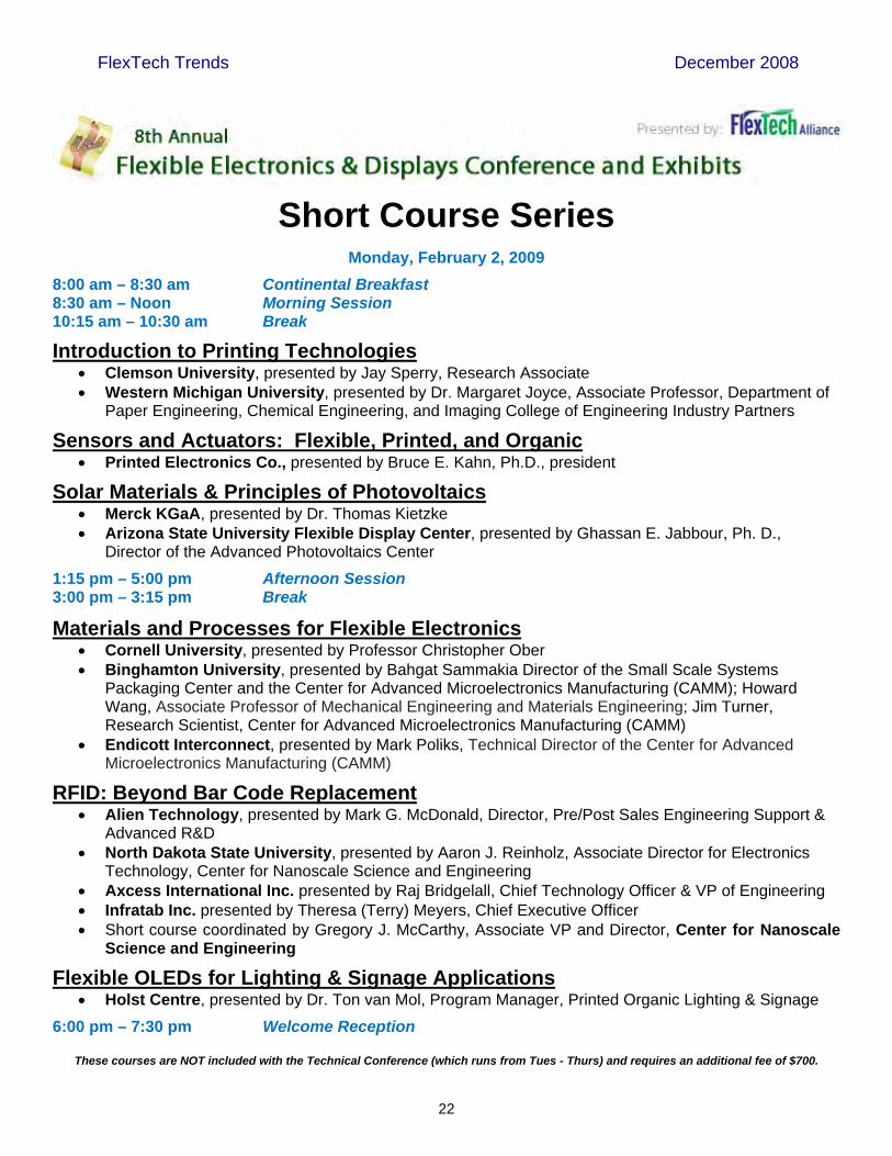
Short Course Series
Monday, February 2, 2009
8:00 am – 8:30 am Continental Breakfast 8:30 am – Noon Morning Session 10:15 am – 10:30 am Break
Introduction to Printing Technologies Clemson University, presented by Jay Sperry, Research Associate Western Michigan University, presented by Dr. Margaret Joyce, Associate Professor, Department of
Paper Engineering, Chemical Engineering, and Imaging College of Engineering Industry Partners
Sensors and Actuators: Flexible, Printed, and Organic Printed Electronics Co., presented by Bruce E. Kahn, Ph.D., president
Solar Materials & Principles of Photovoltaics Merck KGaA, presented by Dr. Thomas Kietzke Arizona State University Flexible Display Center, presented by Ghassan E. Jabbour, Ph. D.,
Director of the Advanced Photovoltaics Center
1:15 pm – 5:00 pm Afternoon Session 3:00 pm – 3:15 pm Break
Materials and Processes for Flexible Electronics Cornell University, presented by Professor Christopher Ober Binghamton University, presented by Bahgat Sammakia Director of the Small Scale Systems
Packaging Center and the Center for Advanced Microelectronics Manufacturing (CAMM); Howard Wang, Associate Professor of Mechanical Engineering and Materials Engineering; Jim Turner, Research Scientist, Center for Advanced Microelectronics Manufacturing (CAMM)
Endicott Interconnect, presented by Mark Poliks, Technical Director of the Center for Advanced Microelectronics Manufacturing (CAMM)
RFID: Beyond Bar Code Replacement Alien Technology, presented by Mark G. McDonald, Director, Pre/Post Sales Engineering Support &
Advanced R&D North Dakota State University, presented by Aaron J. Reinholz, Associate Director for Electronics
Technology, Center for Nanoscale Science and Engineering Axcess International Inc. presented by Raj Bridgelall, Chief Technology Officer & VP of Engineering Infratab Inc. presented by Theresa (Terry) Meyers, Chief Executive Officer Short course coordinated by Gregory J. McCarthy, Associate VP and Director, Center for Nanoscale
Science and Engineering
Flexible OLEDs for Lighting & Signage Applications Holst Centre, presented by Dr. Ton van Mol, Program Manager, Printed Organic Lighting & Signage
6:00 pm – 7:30 pm Welcome Reception
These courses are NOT included with the Technical Conference (which runs from Tues - Thurs) and requires an additional fee of $700.
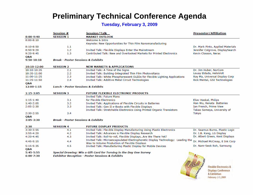
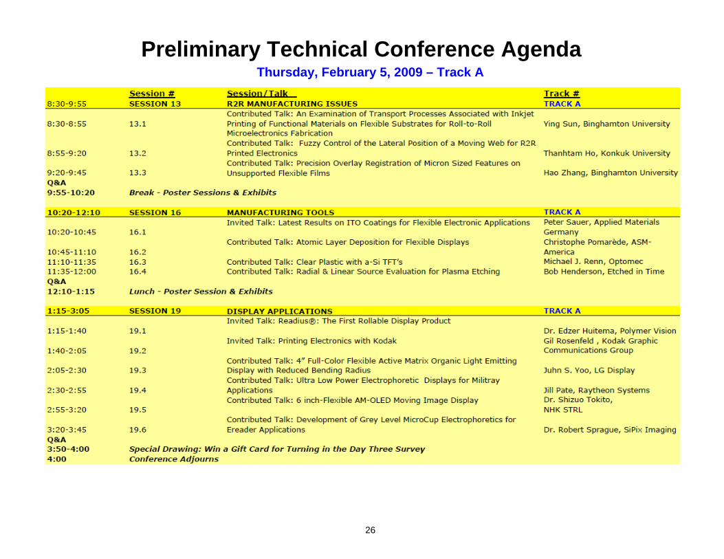
Preliminary Technical Conference Agenda
Tuesday, February 3, 2009

FlexTech Trends December 2008
24
Wednesday, February 4, 2009 – Track A
Preliminary Technical Conference Agenda
FlexTech Trends December 2008
25
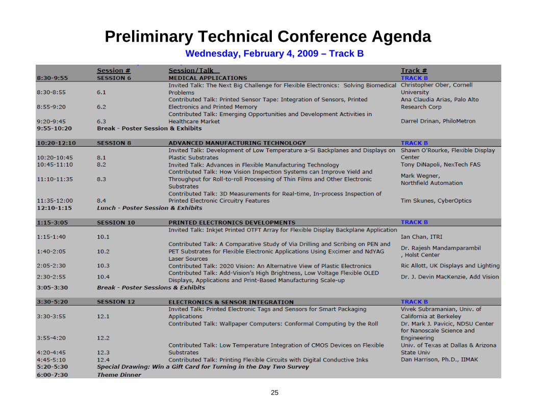
Wednesday, February 4, 2009 – Track B
Preliminary Technical Conference Agenda
FlexTech Trends December 2008
26
Thursday, February 5, 2009 – Track A
Preliminary Technical Conference Agenda

FlexTech Trends December 2008
27
Thursday, February 5, 2009 – Track B
Preliminary Technical Conference Agenda

FlexTech Trends December 2008
28
Thursday, February 5, 2009 – Track C
Preliminary Technical Conference Agenda

Remaking old technologies for the new world of printed electronics
Interview with Jeff Parker from Emerson & Cuming
Jeffrey Michael Parker graduated from the University of Michigan with a Bachelors degree in Chemistry, presently has over twenty years in the field of advanced materials and coating chemistries focusing on electronic applications. Holds patents in the area of designed performance materials for applications in capacitors, batteries, sensors and fuel cells. Has experience at Emerson & Cuming including sister companies for the past nine years with a focus on high speed or web processing applications for printed electronics covering medical, consumer electronic, printed photovoltaic, display and security printing applications. Have worked on a global scale supporting company efforts for printed electronic applications. Presently a member of the SGIA Membrane Switch Council, American Chemical Society, ASTM Membrane Switch Council and presently participating in the FlexTech Alliance initiative to further the development of printed electronics.
Emerson & Cuming, Acheson Colloids, National Starch, Akzo Nobel, ICI, and Henkel – all recently jumbled operations a bit. Can you sort out for us what all happened and the resulting ongoing business that is now being conducted in the area of functional electronic materials? Last year, ICI announced intentions to sell 100% of the company's interest to Akzo Nobel. Akzo Nobel in turn announced that after the sale, they would sell the Electronic Material and Adhesive divisions of National Starch to Henkel. As of April 1, 2008, Henkel in addition to their legacy companies, now owns Abelstik, Emerson and Cuming, and Acheson Colloids. In 2008, the electronic materials group of Acheson Colloids merged with Emerson and Cuming. This included manufacture of conductive or functional inks used in printed electronic applications. Presently Henkel is now one of the largest producers of electronic assembly materials in the world.
So your group, now part of Henkel’s adhesives technology business, is focused on the materials that build-up electronic structures on substrate platforms. What all does this include? The materials that are marketed by Emerson and Cuming include printed inks for electronic applications. The product line includes conductive ink, such as conductive silver, carbon, nickel, silver coated copper and antimony tin oxide. In addition, there are also dielectric products used for applications where insulation is needed for multilayer circuitry, barrier coatings to prevent moisture permeation or for capacitive applications. We also have printed pressure sensitive adhesives that can be used in additive manufacture processes to reduce waste cost and improve process throughput. Emerson & Cuming also has a complete line of conductive and non-conductive adhesives, for assembly of electronic components to flexible and rigid substrates. We also have a series of products aimed at increasing the adhesion strength of components that are used in a wide range of devices such as cellular phones and PCs. These materials are used for underfill, edge-bonding, and encapsulating electronic components typically used to protect components found on circuit boards that are used in challenging environments where vibration and shock would cause failure without application of these materials.
Do you have a particular focus on providing solutions for flexible substrates versus rigid substrates? My focus is aimed at printed flexible electronic applications that are web based or considered to be high speed applications that are recognized in terms of 50 fpm and higher as opposed to sheet fed operations which can be much slower. The solutions or products that we promote for web based printed electronic applications cover a variety of material sets to cover several media types such as solvent- based, Ultraviolet cure and water-based applications. With these products we hope to be able to support most printers with existing equipment print our products successfully.

FlexTech Trends December 2008
30
Please describe your efforts in the membrane switch industry. I recently joined the membrane switch council for the intent of representing our company and our products. The council is now in the process of changing the name to include a wider scope that more accurately depicts the new and emerging markets that we are now beginning to address. One of my tasks was to initiate interest in web based applications by introducing an equipment manufacturer to present at next year's symposium. With this exposure, we hope to show our audience that the traditional method of flat screen printing is not the only approach that can be used to successfully manufacture printed electronic devices.
Membrane switches have generally been excluded from symposia related to flexible electronics, but perhaps this long-standing industry can provide some insights into what might expect as the newer markets emerge. In what ways do you agree or disagree? In my opinion, the knowledge and experience from membrane switch producers can be very useful to emerging printed electronics markets. This stems from the existing knowledge base for the application of materials, test methods and the performance targets that are used for the present membrane switch markets. These three key areas are inherent in the existing experience base and critical to the success of membrane switch manufacturing today. In addition, membrane switch producers have long since been involved in the development of ASTM standards with respect to setting targets and defining test methods. These attributes provide solutions that have enabled materials and processes to meet present targets and can provide support to address shortfalls for future markets.
In your considerations about the market for touch-screens, do you include membrane switches? Will capacitive touch technologies displace membrane switches in the near future? Our products have been widely used for touch screen applications. Present and emerging technology for capacitive touch screens will continue to use our existing products and follow-on generations that we will develop to reduce manufacturing costs and add value to future display products.
In terms of materials related to the touch-screen market, what things are particularly interesting to you? Capacitive applications are attractive due to the robust level of performance that this type of touch screen can possess using our existing materials. With improved performance and increased durability, capacitive switches may prove to open up additional markets for touch screen devices.
Currently you are able to print ITO for non-transparent applications. Do you foresee a day when ITO will be printable as a transparent conductor? What about alternative technologies to ITO? Presently we do not have any printable ITO inks. Printing transparent ITO is difficult to achieve due to the nature of present day particulate technology. Transparent ITO used in applications today is typically sputtered using a thin film processes, which is several orders of magnitude thinner than typical polymer thick films technology can provide. For this reason, printed ITO is only translucent and not transparent due to the particulate nature and the thicknesses achieved. Unless there is a dramatic advance in the technology of ITO materials for polymer thick film applications, it will not approach the transparency and overall performance of sputtered ITO. Alternative technologies to sputtered ITO are beginning to provide similar performance and in time it is my belief that they will eventually displace sputtered ITO as a clear conductive material.
From what markets are you currently deriving most of your revenues? We are heavily involved in consumer electronics which is the source of the majority of our revenue in printed electronics. We also have success in medical, security, display and printed photovoltaic markets as well.
How do you foresee that will change over the next 3-5 years? We see emerging markets such as medical, printed security, and supporting component applications that could grow in the near future. There has been great advancement in the area of printed transistors that would serve essentially any market that would benefit from the reduced cost of printed logic.
Smart cards have seen limited success in Europe; is cost the biggest issue for a more widespread adoption, or are there still some technical limitations that are slowing adoption? Smart cards are used in a variety of applications around the world from subway passes and debit cards in Asia and phone cards in South America to name a few. Adoption of the technology has, in my opinion, been slow in North America, possibly due to security reasons or a failure to embrace new forms of an electronic monetary system. From a
FlexTech Trends December 2008
31
technical aspect, there are countries that have initiated and successfully implemented electronic debit applications for a number of years to the point where it is a necessary function of their daily lives.
Are your customers primarily the printers/converters, or are you selling to device makers directly? In other words, are you getting demand requirements directly from the companies selling the final product or are you one or two steps earlier in the supply chain? Our customers are typically the printers/converters. We do work with end users for the purpose of cooperative development beginning with the design phase. We are finding that this type of arrangement serves to minimize issues later in the manufacturing process.
How do you identify, for example, the composition of an ink that needs to be developed? Do you identify a need and fulfill it on your side, or do you develop new formulations based on requirements from a client? We actually participate in both activities. We tend to be a market driven company so we address the needs of various markets by formulating inks that can provide specific characteristics as well as the type and level of performance needed. We also recognize unique opportunities as well, so we can work towards individual company targets to achieve their end goals.
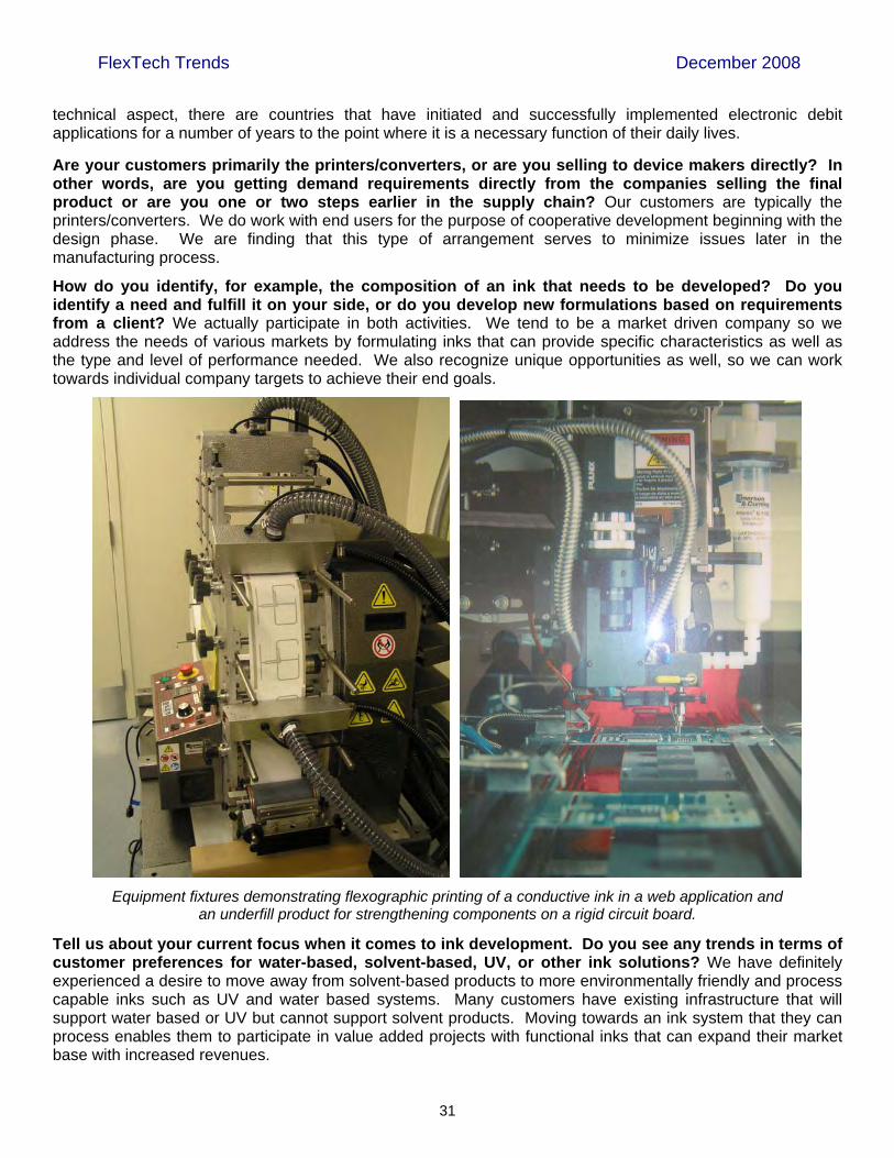
Equipment fixtures demonstrating flexographic printing of a conductive ink in a web application and an underfill product for strengthening components on a rigid circuit board.
Tell us about your current focus when it comes to ink development. Do you see any trends in terms of customer preferences for water-based, solvent-based, UV, or other ink solutions? We have definitely experienced a desire to move away from solvent-based products to more environmentally friendly and process capable inks such as UV and water based systems. Many customers have existing infrastructure that will support water based or UV but cannot support solvent products. Moving towards an ink system that they can process enables them to participate in value added projects with functional inks that can expand their market base with increased revenues.

FlexTech Trends December 2008
32
In terms of printing, it seems your experience is primarily based on analog technologies. Do you see an increase in demand for digital printing solutions and what are you doing in this regard? While it is true that our present focus deals with analog applications, we are looking into digital methods of applying functional inks for printed electronic applications. Again there is a reason that we presently focus on traditional applications processes and that is primarily due to the equipment available at existing and potential customers. Moving towards digital printing requires a significant amount of capital if the change is made purely for printed electronic applications. There will typically need to be great deal of justification to move towards digital and away from technologies that are familiar and available in their facilities.
In terms of flexible electronics, do you see a day when an entire circuit board can be printed? That day is almost here. There are products that enable an entire board to be printed with respect to the traces, resistors and capacitors given enough real estate on the board itself. The logic can be printed, however it is typically much slower than would be commercially viable and would require additional space on the board then presently used for populated components. The real answer that you are looking for is when can we simply place a substrate into some type of printing equipment and have a complete finished board as a result. In my opinion, the ability to produce basic circuit boards that are completely printed with logic may be in the near future. This capability is very attractive because it will change the scope of printed electronics by reducing cost, increasing access on a global scale and enabling advanced technology to improve life in areas that we would have never thought possible just a few years ago.
What’s your guess about when Emerson & Cuming will be printing transistors in a roll-to-roll process? That is a difficult question to address due to the changing technologies that are emerging. Digital printing may change the way we go to market with processes that fit applications. We may need to be cautiously optimistic in the way we think about products and their uses. I would like to see processes that enable roll to roll production in three to five years.
Do you see opportunities in the area of flexible electronics and functional printing processes to develop a manufacturing base in the United States, or do you expect production will shift to Asian sources? There are many opportunities for flexible electronics to flourish in the North America. On a global scale there are many companies that have existing equipment and experience to take on functional printing processes, in addition, the proximity of the manufacturing facility to the developing company is a definite bonus. It is often difficult to design, develop and scale up in a different region for each step in the process for several reasons. The difference in time zones, language and cultural barriers and level of available experience would not make it impossible but would certainly add to the amount of challenges and barriers in shifting to Asian sources. On another note, the cost contributions from labor are minimized when moving towards a high speed applications. This makes a move to a lower cost labor market less attractive when the stringent demands printed electronics are taken into consideration.
What do you hope to gain from your involvement with the FlexTech Alliance? We hope to develop visibility for ourselves as a capable and enabling company through our products, application and customer support. There is also a strong desire to develop relationships that can foster future developments for R&D and for generating commercial success.
Actual photos of a landing pad for an RFID antenna printed with a flexographic water-based ink.

FlexTech Trends December 2008
33

FlexTech Trends December 2008
34

FlexTech Trends December 2008
35
Flexible Displays to Expand in 2009
by Jennifer Colegrove
Jennifer K. Colegrove is Director of Display Technologies at DisplaySearch. She is responsible for reports and consulting projects on display technologies, including flexible displays, OLED, bi-stable displays (e-paper) and low temp polysilicon (LTPS). Before joining DisplaySearch, Dr. Colegrove was a senior analyst at iSuppli and led the emerging display technology services, including touch screen, flexible display, bi-stable displays, LCD, FED, micro displays and OLED. Prior to iSuppli, Dr. Colegrove was a senior display engineer at Intel, performing due diligence for Intel Capital, the venture capital arm of Intel. She was responsible for display technologies from LCD to OLED to bi-stable displays and reviewed all display-related patent applications as a member of the Intel Mobile IP committee. She has also worked in several start-up companies, including dpiX (a Xerox spin-off), Digilens, Silicon Bandwidth and Crystal Research. Jennifer Kong Colegrove has a Ph.D. from Liquid Crystal Institute at Kent State University, Ohio. She received both Master’s and Bachelor’s degrees with honors from Beijing University in Beijing, China.
The age of flexible displays has begun. The light weight, thinness, ruggedness and bendable/rollable form factors have made flexible display increasingly attractive. From segmented electrophoretic displays built on plastic substrates, to high information active matrix displays built on metal foil, plastic, or ultra-thin glass, flexible displays are now penetrating into many applications.
Market forecast: As stated in the recently published Flexible Displays and Electronics Report by DisplaySearch and the FlexTech Alliance, the flexible display market will expand in 2009, and will enjoy significant growth in terms of sales and shipments through 2018:
DisplaySearch forecasts that flexible display revenue will increase from $85 million in 2008 to $8.2 billion in 2018, for a CAGR of 58%. Flexible displays are very complicated with many variable components. The display substrates can be plastic, metal foil, ultra-thin glass, fabric or even paper. The display media can be electrophoretic, electrochromic, bi-stable liquid crystal, conventional liquid crystal, OLED, electroluminescent, or other materials.
Products: Some flexible display products currently in the market include electronic shelf labels and card displays using electrophoretic displays from E Ink and SiPix; card displays made with electrochromic displays from Aveso; wearable displays and advertisement displays made from electroluminescent displays from Wuhan Orient and Shenzhen Guanxing. Flexible active matrix displays will likely enter the market in 2009: the rollable e-book/mobile phone from Polymer Vision is expected to go into production by the end of 2008. Plastic e-newspaper/reader device from Plastic Logic are expected by early 2009.
Flexible display revenue forecast 2008~2018: Source: DisplaySearch Flexible Displays and Electronics Report 2008

FlexTech Trends December 2008
36
Prototypes: At FPD International held in October in Yokohama, LG Display demonstrated a 4-inch flexible AMOLED with stainless steel substrate. It has a thickness of 0.25 mm and a resolution of 320x240 pixels. The phosphorescent OLED materials used in it are from UDC. LG Display has been collaborating with UDC for several years. Samsung Mobile Display (a joint venture of SDI and SEC) demonstrated a flexible AMOLED measuring 6.5 inch in this year’s FPD International. .This might be the second-largest flexible AMOLED ever demonstrated; Sony demonstrated an 11-inch flexible AMOLED at CEATEC 2008. The Samsung flexible AMOLED is built on plastic substrates using LTPS thin film transistors with a resolution of 480x272 pixels.
Another prototype by Samsung Mobile Display is an ultra-thin glass substrate AMOLED, which can be considered as a flexible display. It measures 4-inches in diagonal with 480xRGBx272 resolution, 200 nits brightness, 100K:1 contrast ratio and 100% NTSC color gamut. Samsung indicated that it is made from regular glass substrate which is thinned using the company’s proprietary technique. Toppan Forms and SiPix have collaborated on flexible electrophoretic displays. Their demonstrations included a flexible display
rolled up to a tube shape, card displays and point of purchase/point of sale displays. E Ink demonstrated a flexible display in a curved shape used in a watch featuring a modern design.
Flexible electrophoretic display demonstrators from Toppan Forms, SiPix, and E Ink
Flexible AMOLED display showed by LG Display
On the left is a flexible AMOLED display demonstrated by Samsung, on the right is the thinnest AMOLED, also from
Samsung Mobile Display.

FlexTech Trends December 2008
37
Roll-to-Roll: Simple segmented/passive matrix flexible displays could be built in roll-to-roll facilities. Several roll-to-roll production lines are already built or are being installed, including SiPix, Kent Displays, and Bridgestone.
Active matrix flexible display backplanes are typically produced using batch methods, such as those from Polymer Vision, Prime View International and Plastic Logic. However, some companies are developing roll-to-roll technologies for active matrix as well, such as HP.
Flexible display technology is in rapid development, capacity is being built, and shows great potential for benefits to end-products. In the next couple of years, flexible displays will be seen not only in existing applications but also in new and innovative applications. It has broken the glass ceiling, and now only the sky is the limit.
2009 Flexible Electronics & Displays Conference
Join industry and technology leaders on February 2-5, 2009 in Phoenix, Arizona for FlexTech Alliance’s 8th Annual Flexible Electronics & Displays Conference – the most comprehensive and longest running industry event. Flexible, printed and organic electronics are poised to significantly impact major industries including displays, energy, sensors and medical devices, creating a market in excess of $10B by 2012. Capital equipment and materials investment is expected to show similar growth. If you’re looking to profit from this industry, it’s vital that you attend the 8th Annual Flexible Electronics & Displays Conference.
Join industry and technology leaders from Applied Materials, CMEA Ventures, Heliovolt, Soligie, UC Berkeley, Cornell University and more than 90 other firms and academic institutions to obtain key insights into trends, plans and specific developments in flexible, printed electronics and displays markets and technologies.
Flexible Electronics and Displays 2009 packs an exciting and fact-filled conference with the information you need to succeed in this rapidly growing industry, with over 100 presentations by cutting edge business leaders and technologists, as well as short courses, exhibits, and networking events. There will be 21 conference tracks, including hot topics such as Current Market Outlooks, New Markets and Applications, Future Products, RFID, Photovoltaics, Solid State Lighting & OLEDs, Organic Sensors, and Manufacturing Approaches
New this year! Due to popular demand we’ve added an extra day incorporating a Business & Investment Summit, and expanded the short courses taught by academic and industry leaders. The goal of the Business & Investment Summit is to “Bridge the Information Gap" by connecting innovators and manufacturers of flexible, printed electronics and displays with investors and consumer product developers. The short courses will focus on the emerging field of flexible and printed electronics manufacturing, including photovoltaics, solid state lighting, OLEDs, RFID, sensors, and flexible display applications.
Special Discount for FlexTech Members! For Technical Conference Only (Tues - Thurs), we are offering the special rate of $895! Please use the code "ftdiscount" during registration to receive this rate!
If you are going to attend the Business Summit and the Technical Conference (Monday - Thursday), we are offering an additional $50 off ($895 rate + $50 off the Business Summit). Please use code "ftconfbiz" to receive the discount!
Pointe Hilton Squaw Peak February 2-5, 2009 7677 North 16th Street Phoenix, AZ 85020

FlexTech Trends December 2008
38
iNEMI: Printed Electronics and Nanotechnology
by Alan Rae
Alan Rae is VP of Technology at NanoDynamics Inc. Previously, with Cookson Group plc between 1979 and 2004 he was instrumental in ensuring the success of startup and developed businesses including structural ceramics, flame retardants, refractories, electronic ceramics and wafer plating systems. From 1999 to 2004 he was VP of Technology for Cookson Electronics, deeply involved in developing business opportunities for materials systems and equipment in silicon wafer fabrication, packaging, circuit board manufacture, circuit board assembly and recycling. He is Director of Research for iNEMI Inc. (the International Electronics Manufacturing Initiative), a member and past Chair of the JISSO North America Committee (facilitating electronics business worldwide by harmonizing technology roadmaps and standards), a past member of the Industrial Advisory Board of SMTA (the Surface Mount Technology Association) and a member of the editorial Board of the Bulletin of the American Ceramic Society. He is a member of the ANSI-Accredited US TAG to ISO TC229 (Nanotechnologies) and is the ISO TC229 Task Group Leader for "Nanotechnologies and Sustainability". Dr. Rae holds a Bachelor's Degree from the University of Aberdeen and a Ph.D. and M.B.A. from the University of Newcastle upon Tyne. He is a member of the Royal Society of Chemistry and a Chartered Chemist.
The collection of synthesis tools collectively known as “nanotechnology” allows us to create a range of materials which present many opportunities to reshape the electronics industry from top to bottom. Printed electronics especially can benefit from the use of these new materials. Nanotechnology can offer us:
• Uniform particles – metal, oxide, ceramics, composite • Reactive particles – particularly metals • Unusual optical, thermal and electronic properties for phosphors, heat pipes, and percolation based
conductors. • Nano-structured materials – tubes, balls, hooks, novel textured surfaces. • Self-assembly – liquid-based, vapor based or even by diffusion in the solid state.
iNEMI is an industry-led consortium of approximately 70 electronics manufacturers, suppliers and related organizations. The iNEMI roadmap (http://www.inemi.org) is a biennial comprehensive survey that reviews the key issues affecting the electronics supply chain. Gaps in the technology or infrastructure that could adversely affect iNEMI members worldwide are identified, and the NEMI Research Committee was formed in 2004 to prioritize and disposition the gaps identified in the roadmap process, and identify companies, universities and government laboratories that can address them for the mutual good.
The use of printing or dispensing techniques for solder paste, adhesives and underfills is well established in electronics packaging, displays and assembly but many new printed applications are evolving. Including traditional and novel materials systems, the “Printed Electronics” Technology Working Group (TWG) has evolved in 2008 into the “Large Area Flexible Electronics” TWG to reflect the evolution and breadth of these business opportunities. As can be seen below in the categories described in the 2007 roadmap there are many permutations and combinations of industries, applications, functionality and printing technology, with lateral resolutions and deposition thicknesses as low as 10 microns and 0.01 microns respectively.
Critical barriers to the development of large area flexible electronics identified in 2007 roadmap included the following needs:
In-line quality control measurement equipment. Higher performance solution processable semiconducting inks. The availability of a hybrid printing/manufacturing platform utilizing a range of different printing
techniques. Simulation tools to bridge the gap between microelectronics and graphics design software. Increased customer “pull”.
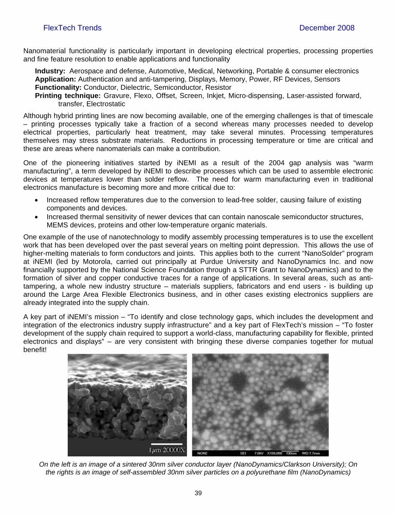
FlexTech Trends December 2008
39
Nanomaterial functionality is particularly important in developing electrical properties, processing properties and fine feature resolution to enable applications and functionality
Industry: Aerospace and defense, Automotive, Medical, Networking, Portable & consumer electronics Application: Authentication and anti-tampering, Displays, Memory, Power, RF Devices, Sensors Functionality: Conductor, Dielectric, Semiconductor, Resistor Printing technique: Gravure, Flexo, Offset, Screen, Inkjet, Micro-dispensing, Laser-assisted forward,
transfer, Electrostatic
Although hybrid printing lines are now becoming available, one of the emerging challenges is that of timescale – printing processes typically take a fraction of a second whereas many processes needed to develop electrical properties, particularly heat treatment, may take several minutes. Processing temperatures themselves may stress substrate materials. Reductions in processing temperature or time are critical and these are areas where nanomaterials can make a contribution.
One of the pioneering initiatives started by iNEMI as a result of the 2004 gap analysis was “warm manufacturing”, a term developed by iNEMI to describe processes which can be used to assemble electronic devices at temperatures lower than solder reflow. The need for warm manufacturing even in traditional electronics manufacture is becoming more and more critical due to:
Increased reflow temperatures due to the conversion to lead-free solder, causing failure of existing components and devices.
Increased thermal sensitivity of newer devices that can contain nanoscale semiconductor structures, MEMS devices, proteins and other low-temperature organic materials.
One example of the use of nanotechnology to modify assembly processing temperatures is to use the excellent work that has been developed over the past several years on melting point depression. This allows the use of higher-melting materials to form conductors and joints. This applies both to the current “NanoSolder” program at iNEMI (led by Motorola, carried out principally at Purdue University and NanoDynamics Inc. and now financially supported by the National Science Foundation through a STTR Grant to NanoDynamics) and to the formation of silver and copper conductive traces for a range of applications. In several areas, such as anti-tampering, a whole new industry structure – materials suppliers, fabricators and end users - is building up around the Large Area Flexible Electronics business, and in other cases existing electronics suppliers are already integrated into the supply chain.
A key part of iNEMI’s mission – “To identify and close technology gaps, which includes the development and integration of the electronics industry supply infrastructure” and a key part of FlexTech’s mission – “To foster development of the supply chain required to support a world-class, manufacturing capability for flexible, printed electronics and displays” – are very consistent with bringing these diverse companies together for mutual benefit!
On the left is an image of a sintered 30nm silver conductor layer (NanoDynamics/Clarkson University); On the rights is an image of self-assembled 30nm silver particles on a polyurethane film (NanoDynamics)
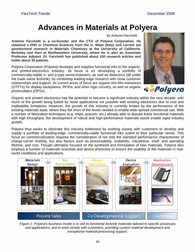
FlexTech Trends December 2008
40
Advances in Materials at Polyera
by Antonio Facchetti
Antonio Facchetti is a co-founder and the CTO of Polyera Corporation. He obtained a PhD in Chemical Sciences from the U. Milan (Italy) and carried out postdoctoral research in Materials Chemistry at the University of California-Berkeley and then at Northwestern University, where he is also an Associate Professor Adjunct. Dr. Facchetti has published about 150 research articles and holds about 30 patents.
Polyera Corporation (Polyera) develops and supplies functional inks to the organic- and printed-electronics industry. Its focus is on developing a portfolio of commercially-viable n- and p-type semiconductors, as well as dielectrics (all under the trade name ActivInk), by combining leading-edge research with close customer relationships and support. Its current areas of focus are organic thin-film-transistors (OTFTs) for display backplanes, RFIDs, and other logic circuitry, as well as organic photovoltaics (OPVs).
Organic and printed electronics has the potential to become a significant industry within the next decade, with much of the growth being fueled by novel applications not possible with existing electronics due to cost and malleability limitations. However, the growth of this industry is currently limited by the performance of the existing materials base, where they fall short of the levels needed to enable wide-spread commercial use. With a number of fabrication techniques (e.g. inkjet, gravure, etc.) already able to deposit these functional materials with high throughput, the development of robust and high-performance materials would enable rapid industry growth.
Polyera thus seeks to eliminate this industry bottleneck by working closely with customers to develop and supply a portfolio of leading-edge, commercially-viable functional inks suited to their particular needs. This focus on commercialization requires the consideration of not only the standard performance characteristic of charge-carrier mobility, but also factors such as processability, scalability, robustness, shelf- and operating lifetime, and cost. Though ultimately focused on the synthesis and formulation of new materials, Polyera also employs a number of materials scientists and device physicists to ensure the usability of the materials in real-world conditions and applications.
Figure 1: Polyera’s business model is to sell its functional ActivInk materials tailored to specific processes and applications, and to work closely with customers, providing custom material development and
exceptional material-processing support.
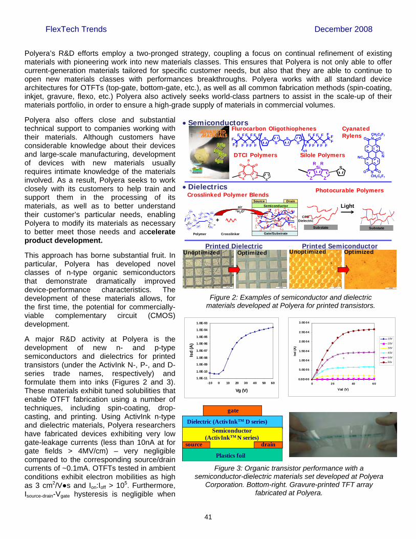
FlexTech Trends December 2008
41
Polyera’s R&D efforts employ a two-pronged strategy, coupling a focus on continual refinement of existing materials with pioneering work into new materials classes. This ensures that Polyera is not only able to offer current-generation materials tailored for specific customer needs, but also that they are able to continue to open new materials classes with performances breakthroughs. Polyera works with all standard device architectures for OTFTs (top-gate, bottom-gate, etc.), as well as all common fabrication methods (spin-coating, inkjet, gravure, flexo, etc.) Polyera also actively seeks world-class partners to assist in the scale-up of their materials portfolio, in order to ensure a high-grade supply of materials in commercial volumes.
Polyera also offers close and substantial technical support to companies working with their materials. Although customers have considerable knowledge about their devices and large-scale manufacturing, development of devices with new materials usually requires intimate knowledge of the materials involved. As a result, Polyera seeks to work closely with its customers to help train and support them in the processing of its materials, as well as to better understand their customer’s particular needs, enabling Polyera to modify its materials as necessary to better meet those needs and accelerate product development.
This approach has borne substantial fruit. In particular, Polyera has developed novel classes of n-type organic semiconductors that demonstrate dramatically improved device-performance characteristics. The development of these materials allows, for the first time, the potential for commercially-viable complementary circuit (CMOS) development.
A major R&D activity at Polyera is the development of new n- and p-type semiconductors and dielectrics for printed transistors (under the ActivInk N-, P-, and D-series trade names, respectively) and formulate them into inks (Figures 2 and 3). These materials exhibit tuned solubilities that enable OTFT fabrication using a number of techniques, including spin-coating, drop-casting, and printing. Using ActivInk n-type and dielectric materials, Polyera researchers have fabricated devices exhibiting very low gate-leakage currents (less than 10nA at for gate fields > 4MV/cm) – very negligible compared to the corresponding source/drain currents of ~0.1mA. OTFTs tested in ambient conditions exhibit electron mobilities as high as 3 cm2/V●s and Ion:Ioff > 105. Furthermore, Isource-drain-Vgate hysteresis is negligible when
Figure 2: Examples of semiconductor and dielectric materials developed at Polyera for printed transistors.
Semiconductors
Dielectrics
+
Polymer
CPBDielectric
“H2O”air
Crosslinker
Source Drain
Semiconductor
Gate/Substrate
Printed Dielectric Printed SemiconductorUnoptimized OptimizedUnoptimized Optimized
Flurocarbon Oligothiophenes CyanatedRylens
Crosslinked Polymer BlendsPhotocurable Polymers
Silole Polymers
SiR R
ZZ
S
SS
SS
F F
F F
F F
F F
F FF
F F
F
FF
F F
F F
F F
F F
F Fn/4
N
N
OO
OOCH2C3F7
CH2C3F7
CNNC
N
S
OO
R
S S
DTCI Polymers
Light
Substate Substate
drain
Plastics foil
Dielectric (ActivInkTM D series)
Semiconductor(ActivInkTM N series)
source
gate
1.0E-11
1.0E-10
1.0E-09
1.0E-08
1.0E-07
1.0E-06
1.0E-05
1.0E-04
1.0E-03
-10 0 10 20 30 40 50 60
Vg (V)
Isd
(A
)
0.0E+00
5.0E-05
1.0E-04
1.5E-04
2.0E-04
2.5E-04
3.0E-04
0 20 40 60
Vsd (V)
Isd
(A
)
10V
20V
30V
40V
50V
60v
c
Figure 3: Organic transistor performance with a semiconductor-dielectric materials set developed at Polyera
Corporation. Bottom-right. Gravure-printed TFT array fabricated at Polyera.

FlexTech Trends December 2008
42
the OTFTs are tested for different Vgate scan rates (1V/s - 50V/s) demonstrating excellent insulator-semiconductor interfacial properties.
Collaboration with the University of Greningen (The Netherlands), researchers demonstrated the realization of bottom-contact, bottom-gate field-effect transistors (OFETs) with only ~ 3 m channels based on spin-coated films of ActivInk N1100 (N,N’-1H,1H-perfluorobutyl-dicyanoperylenedicarboxiimide; PDI-F-CN2). ActivInk N1100 combines excellent semiconductor properties with good solution-processability. After deposition of the spin-coated films, high mobility values are obtained after a low-temperature thermal treatment that induces high crystalline organization of the molecules in the film. To rationalize the electrical characteristic variations upon annealing, the semiconductor film morphologies were investigated by atomic force microscopy (AFM) and confocal laser microscopy (CLM). Interestingly, the AFM images demonstrate that the pristine semiconductor film morphology is characterized by rough protruding features (RMS roughness of ~ 30 nm). After thermal annealing, the ActivInk N1100 film is smooth and uniform, exhibiting small rounded protrusions (RMS roughness ~ 1.5 nm). The film roughness is comparable with that of the substrate, an indication of highly crystalline organization. The difference in the ActivInk N1100 film optical micrographs and in the photoluminescence images obtained by confocal laser microscopy provides further demonstration of the enhanced order of the annealed films. From the wide-field micrographs of Figure 4, the pristine film is inhomogeneous. When excited at 514 nm it exhibits an intense photoluminescence emission.
This is due to poor film crystallinity, or small microcrystalline domains oriented randomly with respect to the substrate. However, after film thermal annealing the wide-field micrograph acquired under the same conditions appear completely different, with the film surface becoming smooth and transparent to the impinging light. In addition, when measured in the same conditions of the no-thermally treated sample, the photoluminescence emission intensity from the zone within the device channel is strongly reduced, an indication of the greatly improved molecular order (Figure. 4d). This data suggest an edge-on orientation of the ActivInk N1100 molecules, which causes a weaker coupling between the transition dipole moment of the molecules of the film and the electric field of the impinging laser beam, resulting in a reduced absorption of the light and consequently in a weaker photoluminescence emission. The edge-on molecular orientation on the dielectric surface is fundamental to achieve efficient OFET charge transport.
Another key area of development at Polyera is in supplying materials for circuit applications. Very successful projects have involved the fabrication of bottom-gate complementary circuits in collaboration with OrganicID (USA) and the first demonstration of solution-processed top-gate transistors and complementary circuits carried out with PolyIC (Germany). In these projects, researchers first fabricated several transistor structures to demonstrate the potential of ActivInk N1200 ((N,N’-dioctyl-dicyanoperylenedicarboxiimide; PDI-8CN2). The devices fabricated with solution-processed ActivInk N1200 combined with solution-processed ActivInk D1400 (a photo-crosslinkable polymer) exhibit mobilities as high as ~ 0.1 cm2/Vs with an average mobility of ~ 0.05 cm2/Vs, and Ion:Ioff ratios are ~ 104.
Figure 4: Output voltage of a field-effect transistor based on solution-processed ActivInk N0500. Wide-field micrographs of the spin-coated PDI-FCN2: b) directly after the deposition d)
after the annealing process at 110°C in a vacuum oven for one hour. Confocal fluorescence images of the spin-coated PDI-FCN2: c) directly after the deposition e) after the annealing
process at 110°C in a vacuum oven for one hour.
a b c
d e

FlexTech Trends December 2008
43
In collaboration with OrganicID, Polyera fabricated the first bottom-gate inkjet-printed CMOS circuits operating in ambient. Five-stage complementary ring oscillators and complementary pass transistor logic based D flip-flops were fabricated with ActivInk N1200 solution-deposited n-channel FETs and P3HT solution-deposited p-channel FETs. These CMOS circuits, consisting of both p-channel and n-channel transistors, are an ideal configuration for organic semiconductors, offering low static power dissipation, crucial for the portable, often battery operated applications envisioned for organic electronics, and the superior noise margins which relax the requirement for large Ion/Ioff ratios. The channel width (W) and channel length (L) of the individual transistors were 2000 µm and 7.5μm, respectively. Discrete OFETs for CMOS circuits were characterized in vacuum and in air. The saturation region mobility of these OFETs is ~10-2 cm2/Vs.
A ring oscillator, often used in clock generation circuits, was fabricated by connecting an odd number of inverters in a loop. The ring oscillator operating frequency is a measure of the maximum speed at which digital
circuits can be operated, and the maximum switching frequency of a single transistor is a function of the mobility, terminal voltages, and channel length as well as parasitic capacitances. Figure 5 shows the output characteristics of a five-stage ring oscillator with a 100 V supply and a channel length of 7.5μm. Frequencies of 3.2 kHz and 2.2 kHz are achieved in vacuum and in ambient atmosphere at room temperature, respectively. A conventional organic CMOS master-slave D flip flop was also characterized. The D flip flop is a critical part of sequential logic circuits. An edge-triggered D flip flop is usually composed of two level sensitive latches and each latch consists of two CMOS transmission gates and two inverters. All D flip flop electrical characterizations were carried out in ambient at room temperature. Measured characteristics for the pass transistor logic-based D flip-flop at clock frequencies of 500 Hz and 1.6 kHz at a supply voltage of 100 V are shown in Figure 6. Speed is limited by one transmission gate and one inverter delay after the clock converts from logic 0 to 1. Output Q begins to degrade at 1.6 kHz, however, it is still controlled by the clock signal. These results represent the first organic CMOS circuits
Figure 6A: Characteristics of ActivInk N1200 solution-processed bottom contact OTFT. Figure 6B: Ring oscillator based on PDI-8CN2 (n-channel FETs) and poly(3-hexyl)thiophene (P3HT, p-
channel FETs) solutions. The supply voltage was 100 V. (W / L = 2,000 μm / 7.5 μm) and the oscillation frequency of 3.2 kHz Figure 6C: Schematic diagram of conventional D flip-flop
operating at 500 Hz (top) and 1.6 kHz (bottom).
B.
N-OFET
Ring Oscillator
C. D Flip FlopA.
Figure 5A: Schematic of a five stage complementary ring oscillator without buffer stage. Figure 5B: Oscillation of 34 kHz in a ring
oscillator with Vsupply =100 V.

FlexTech Trends December 2008
44
based solely on solution-deposited active semiconductors, and represent a major step forward in developing printed organic electronic circuits with high switching speeds, low noise margins, and low power dissipation.
With PolyIC, Polyera demonstrated top-gate TFTs and the first solution-processed top-gate organic CMOS circuits on poly(ethyleneterephtalate) (PET) operating in ambient (Figure 7). By combining an odd number of complementary inverters, researchers fabricated the first top-gate CMOS ring oscillators with different numbers of stages. For instance Figure 7 shows a picture of a 7 stage ring oscillator consisting of 7 n-TFTs and 7 p-TFTs. In these devices, the output signal is measured via another inverter (1 n-TFT + 1 p-TFT). Using this setup, a negative supply voltage is necessary. The circuit starts oscillating, when a negative DC supply voltage |VBsupB| > 10 V is applied. Figure 7 shows the signal of a 9 stage ring oscillator measured at -12V supply voltage. The oscillation frequency of this device is 75 Hz. The levels of the ring oscillator nearly correspond to GND and VBsupB, respectively. This is again a clear feature of CMOS technology. To investigate the long term stability of these top-gate TFTs, the ring oscillator was tested after storage for more than 9 months in aerated dark containers. Negligible variation in signal amplitude (~ +3%) and minimal frequency changes (~ -15%, red line) are recorded demonstrating the good stability of these ambient-fabricated and unencapsulated devices.
Recently, Polyera has been collaborating with IMEC (Belgium) to use electron-transporting materials (ActivInk
N0700; α, ω-diperfluorohexyl-quaterthiophene) for the fabrication of OLED with remote metallic electrodes. This light-emitting device, shown in Figure 8, is a light-emitting diode in which the electron-transporting layer is implemented as the accumulation channel of an electron-conducting organic thin-film transistor (OTFT). Thanks to the high field-effect mobility that can be achieved in an electron accumulation channel, electrons can be transported over several micrometers. Furthermore, similar to the case of light-emitting transistors, the current density can be significantly high in these OLEDs. As the light-emission zone of the OLED is not covered by metal, the device can be used for top-emission or even as a waveguide.
ActivInkTM D0700ActivInkTM D0700a b c
Figure 8a: Schematic cross-section of the organic light-emitting diode with field-effect-assisted electron transport. Figure 8b: Normalized absorption spectrum of a thin film of ActivInk D0700 (blue
curve) and photoluminescence spectrum of Alq3:DCM2 (red curve). Figure 8c: The external quantum efficiency as a function of the current.
This high current density, combined with reduced optical absorption losses due to the remote metallic cathode, may be beneficial to high-brightness OLEDs, and potentially useful as a concept for organic laser structures.
Figure 7: Schematic representation of a top-gate bottom-contact transistor (top) and optical image of the seven-stage
ring oscillator fabricated on plastic.
FlexTech Trends December 2008
45
The maximum external quantum efficiency achieved by these OLEDs with a remote cathode was however rather low (0.02%). The use of a high-mobility, wide-bandgap electron-conducting semiconductor material such as ActivInk N0700 used in combination with Alq3:DCM2 as the host-guest fluorescent system allows high electron-current densities combined with a much improved quantum efficiency. The measured maximum external quantum efficiency of these devices is 0.25%, which is more than 10 times larger than the value we obtained for devices employing other electron-transporting material.
References
2. a) Facchetti, A. Nature Mater. 2008, 7, 839. b) de Boer, B; Facchetti, A Polymer Reviews 2008, 48, 423. c) Facchetti, A. Angew. Chem. Int. Ed. 2007, 46, 1367. d) Facchetti, A. Materials Today 2007, 10, 28.
2. a) Jones, B. A.; Facchetti, A.; Wasielewski, M. R.; Marks, T. J. J. Am. Chem. Soc. 2007, 129, 15259. b) Wang, Z.; Facchetti, A.; Marks, T. J. J. Am. Chem. Soc. 2007, 129, 13362. c) Jones, B. A.; Facchetti, A.; Marks, T. J.; Wasielewski, M. R. Chem. Mater. 2007, 19, 2703. d) Yoo, B.; Jung, T.; Basu, D.; Dodabalapur, A.; Jones, B. A.; Facchetti, A.; Wasielewski, M Appl. Phys. Lett., 2006, 88, 082104. e) Jones, B. A. Anhis, M. J. Yoon, M.-H. Facchetti,. A. Marks, T. J. Wasielewski M. R. Angew. Chem. Int. Ed. 2004, 43, 6363.
3. Yan, H.; Zheng, Y.; Blache, R.; Newman, C.; Lu, S.; Woerle, J.; Facchetti, A. Adv. Mater. 2008, 20, 3393. 4. Schols, S.; McClatchey, C.; Rolin, C.; Bode, D.; Genoe, J.; Heremans, P.; Facchetti. A. Adv. Func. Mater.
2008, 18, 3645.
Flexible Displays and Electronics Report
Are flexible displays finally ready for mass adoption?
The 300+-page Flexible Displays and Electronics Report contains detailed data and unparalleled analysis on the readiness of various flexible display technologies and their commercial opportunities.
In this new report, DisplaySearch and the FlexTech Alliance forecasts that flexible display revenue will increase from $85M in 2008 at a compounded annual growth rate of 58% to $8.2B in 2018. In addition to market forecasts by technology and application, this comprehensive report covers:
Market readiness of core technologies, suppliers, and manufacturers
Market drivers impacting the growth of flexible displays and electronics
Analysis of electrophoretic, electrochromic, OLED, RFID, flexible substrates, active matrix backplanes and more
Product roadmaps and capacity by technologies and applications
Contact us today for more information on the Flexible Displays and Electronics Report and how you can get a complimentary copy of the 85-page Flex Tech Alliance (with assistance from cintelliq) report “Flexible Electronics: Government Investment and R&D Programs in the U.S. and European Union”.

FlexTech Trends December 2008
46
Liquid Crystals and more from EMD Chemicals An affiliate of Merck KGaA, Darmstadt, Germany
by Bob Miller
Bob Miller is the Business Manager of Organic Electronics and Photovoltaics for EMD Chemicals, the North American specialty chemicals affiliate of Merck KGaA, Darmstadt, Germany. Mr. Miller is responsible for pursuing new business opportunities in the printable electronic, photovoltaic and touch panel industries, and developing working relationships with customers and technology development partners. Mr. Miller joined EMD Chemicals in Central Product Management in 2002, responsible for management of the Pigments Division product portfolio, moved to Corporate Business Development in 2005 and assumed his current role in the Liquid Crystals Division in 2007. Bob has a Masters of Business Administration from Fordham University of New York as well as a BS in Chemistry from CUNY and an MS in Polymer Chemistry.
Sharper, faster, larger and, above all, ubiquitous – that is a brief description of the global success story of LC displays. Whether it is a cell phone, a smart phone or a wireless notebook computer, today we can be connected to each other anywhere we go in the world at anytime. A key enabling technology behind this global access to information is liquid crystals: high-tech materials having unique characteristics that enable lightweight, portable, energy-saving electronic displays. This technological development has changed and enhanced our lives forever in ways we are still discovering.
In the very same spirit of discovery, we are advancing developments in the field of organic electronics. We believe that large-area, continuous-printing-process-based manufacturing is going to open up a host of new and exciting applications. A key element for this to happen is again a high-tech material class, the soluble organic semiconductor. To take display applications as an example, we anticipate the use of conventional printing processes for fabricating transistor arrays for backplanes for driving standard rigid LCDs. These materials also enable other emerging technologies. Their use in flexible displays offer product designers the potential to change how, when and where we have the capability to access information in either static or dynamic, black and white or color, and still or video formats.
We also believe that this same high throughput, low cost process will be the basis of competitive, on and off grid, printable photovoltaics. This technology also has the potential to enable an alternative to fossil-fuel-based energy. To that end, we have and continue to invest heavily in research and development in these areas at our research centers around the globe. For example, at the Advanced Technology Centre in Chilworth, UK, we are extending our building to accommodate and expand our research efforts in the aforementioned PV and flexible display applications. Our previous research investments there have resulted in the development of unique organic semiconductor materials for which Merck KGaA has been recognized.

FlexTech Trends December 2008
47
Merck/EMD offers a product range of organic semiconductor, dielectric and ancillary materials, marketed under the lisicon trade name, to enable solution printing of the integrated circuitry that will underpin these applications. These innovative materials are based on conjugated aromatic molecules with delocalized electronic systems, designed to exhibit optimum charge transport properties for transistors or light absorption and conversion properties for photovoltaics. We incorporate these materials into ready-to-use ink formulations, specifically designed for a range of coating or printing processes. Synthesis of these specialty materials is carried out under the high-purity conditions required to achieve reproducible high performance electrical characteristics.
In addition to the activities to commercialize our lisicon organic electronics materials, there is a significant R&D commitment for the advancement of inorganic solutions, mainly focused on printable radio frequency identification (RFID) chips. An interdisciplinary research group has been working on this in the MerckLab at the Technical University of Darmstadt (TUD), a well-known center of printing knowledge. The goal of the project is to reduce the manufacturing costs of the RFID chips. Researchers there are exploring the use of mass production processes -- in particular, conventional printing methods to place the chips directly onto product packaging. In this laboratory, vanishingly small quantities of dispersed or soluble inorganic-based formulations can be tested for their printing characteristics. Various printing methods – such as offset printing, screen printing and ink jet printing – are available in this laboratory. The scientists’ contacts with renowned manufacturers of printing machines ensure that the team is always working with state-of-the-art know-how and equipment in this process.
At our research labs in Atsugi, Japan, Merck researchers are working on third-generation photovoltaics, such as dye-sensitized solar cells (DSSC) and nanotechnology for electronics and solid-state lighting applications. Our experts in Asia collaborate closely with university scientists. The high scientific competence of our colleagues in Japan, for example, has been recognized by, among others, the Japanese Ministry of Economy, Trade and Industry (METI). Several years ago, Merck was the only non-Japanese company to participate in various joint research projects.
And now in the US, Merck is actively investing in R&D. In 2008, EMD opened its Advanced Technology Lab in Cambridge, MA. This laboratory’s mission is to develop the materials platform for the next generation of electronics. The focus is on new inorganic materials platforms with concentration in optoelectronic applications such as printable electronics, photovoltaics and displays. The location of the site was chosen to tap into the considerable local innovation infrastructure as well as the wider US technical community.
To successfully advance the science and move the materials and technology towards commercialization, we engage in selected, intensive, collaborative relationships with our business partners. These contractual-based partnerships allow both parties to secure their respective intellectual property developments while at the same time allowing open sharing of information and results in an iterative feedback process. Schematically, this is represented below.
These continued investments in R&D have paid off in the past and will pay off in the future. It has allowed Merck/EMD to be the leading company in new high-tech materials for electronics manufacturing purposes, well positioned to be the partner of choice when it comes to innovative material concepts for next-generation electronics. We embrace the opportunity that the development of new materials technology presents to us to offer solutions to problems and provide tools for creating entirely new products that improve and enrich the quality of all of our lives.

FlexTech Trends December 2008
48
The Next Steps in the Growth of an Industry
by J. Kevin Cammack
Dr. Kevin Cammack joined FlexTech in January, 2008 as Director of Technical Marketing and Corporate Development, where he is responsible for technical and market reporting and analysis; management of project contracts; and outreach activities to the financial and entrepreneurial communities. Kevin is a graduate of Stanford Graduate School of Business, earned his Ph.D. in organic chemistry from the University of California, Berkeley and his BS (Phi Beta Kappa) from the University of Florida.
This quarter’s issue is really about innovative firms overcoming fundamental challenges in materials. As the flexible and printed electronics industry moves forward, materials and process development will continue to be at the heart of new growth – the emerging products that drive that growth will all require advances in some area related to materials properties. The pioneering work by Emerson and Cuming, Polyera and EMD highlighted in this issue are great examples of materials development driving the industry to where it is today.
The flexible and printed electronics industry is at a critical point in its growth. 2008 saw the emergence of multiple flexible display products, including Polymer Vision’s Readius and E-Ink’s amazing collaboration with Esquire to incorporate an E-Ink digital display into the cover of their October issue.
In other areas, notably photovoltaics, transitional technologies went from essentially interesting ideas to volume production and mainstream acceptance. First Solar, with their high volume, continuous thin-film Cadmium Telluride solar manufacturing technology, for example, went from being off the radar in 2006 to the fifth largest manufacturer of solar cells in the world in 2007 [Solar Buzz].
Both Applied Materials and Oerlikon have adapted display technology for the creation of high throughput amorphous Silicon solar cells, and started shipping turnkey production lines this year. The first products off an Applied Materials SunFab line are expected sometime in Q4 of this year. These high throughput sheet-fed tools are precursors to the continuous roll-to-roll production tools of the future.
All of this activity points to the next major milestone that must be met for sustainable high-volume production of printed electronics – standardization of production toolsets and materials. This fall, the FlexTech Alliance held two workshops – The Inks and Materials Technology Working Group meeting at Western Michigan University (co-sponsored by Emerson and Cuming) and the Quarterly Workshop on Photovoltaics at HP labs in Palo Alto, California. In both workshops, industry participants drove the agenda, and overwhelmingly indicated a need for a standardization of materials benchmarking, and a materials registry database as a precursor to the development production processes.
FlexTech is working towards that goal with its most recent RFP. This hurdle is easily overcome if everyone pulls together, but a show stopper if not. As a neutral player representing multiple parts of the value chain, FlexTech is in a unique position to navigate these waters, but we need your support and participation to do it.
Investing In the Flexible Future: Of course, success in flexible and printed electronics requires more than just innovative materials development. The entire value chain needs to be built, from scratch. This means developing multiple industries at the same time – the products are too complex for any one firm to vertically integrate across the entire ecosystem. Industry leaders such as E-Ink and Plastic Logic have learned this the hard way – by trying it. Ultimately both firms scaled back their grand visions to focus on their core competencies.
Figure 1: The October issue of Esquire, with E Ink cover

FlexTech Trends December 2008
49
Building an entire manufacturing ecosystem from scratch is an expensive investment, with tremendous gains for society. Unfortunately the complexity of the process and the nature of the problems that need to be solved to start production means that the innovator who creates something of general interest to the industry either must jealously guard his interests and restrict his intellectual property or make it widely available and give away most of the value. This is a situation where government investment can create huge benefit to the common good by reducing the risks individual firms take, and by creating a public license for the intellectual property generated from the investment.
The government that invests strongly in this work ends up with a flourishing growth industry, while countries that don’t invest end up spending huge amounts of capital to catch up. There is an opportunity today for the US to leverage our leadership in technology development to become global leaders in the potentially multi-billion dollar flexible and printed electronics industry. And yet… The US is not keeping up with investment in this area. The EU has taken the leadership role, and by all appearances intends to keep it.
Both the European Union (EU) and the United States (US) governments have been investing in the flexible and printed electronics industry since 2001, including significant commitments for funding through the end of 2013. The combined total commitment of government funds to flexible and printed electronics is just over $1 Billion over the period 2001 – 2013. Of this total, the EU commitment is $719M, almost 2.5 times the commitment of $327M by the US government.
The apparent disparity in funding for flexible and printed electronics between the EU and the US is far larger than the overview in Figure 3 suggests. Programs specifically aimed at flexible and printed electronics are more common in the EU – $507M (€332M) in the EU versus $200M in the US. Printed electronics provides one of the few opportunities for the US to recapture electronics manufacturing that has flown to Asia over the last 20 years. If the US is to maintain the leadership provided by our innovation, government investment is critical to get the industry past barriers that are impossible for any one company to monetize – things like standardization of benchmarks, development of a materials registry, and the development of common toolsets for both design and production.
FlexTech is committed to changing this dynamic and forging the printed electronics ecosystem in the US. By bringing together public and private interests in the industry FlexTech is working on turning the tide and making the US a leader once again. However, this takes commitment from more than just FlexTech – it requires effort from everyone in the ecosystem. If you are an industry such as federal, state or local government, print shops, chemical/materials manufacturing, capital equipment, consumer products, computer hardware or other high tech area, and even investing in these areas, I strongly encourage your organization to join FlexTech today and help make flexible and printed electronics a reality.
Figure 2: AKT SunFab amorphous-Silicon production line and solar cells that come off the line
Figure 1: Government Investment in Flexible and Printed Electronics

FlexTech Trends December 2008
50
FFrreeqquueennttllyy aasskkeedd qquueessttiioonnss aabboouutt FFlleexxTTeecchh AAlllliiaannccee
Why the FlexTech Alliance? Industry analysts predict that the flexible and printed electronics industry will be a $50B market by 2017. The flat panel display market, while maturing, will still grow 25% in 2008. The FlexTech Alliance will offer North American companies and institutions engaged in flexible, printed electronics and displays the most comprehensive membership program, including:
Networking & collaboration opportunities with potential partners and customers Regular updates on technology trends and industry developments through reports available on-line
at http://www.flextech.org Pre-competitive R&D funding opportunities Industry advocacy at the federal and state level
Why did USDC decide to go in this direction? Several years ago, USDC initiated a shift in its R&D funding strategy to enable flexible substrates and tooling for flexible displays and roll-to-roll (R2R) processing. Soon after this shift took place, it became apparent that displays were not the only market for USDC member companies and their supply chain. As a result, USDC created the Flexible, Printed and Organic Electronics Initiative, which was launched in December 2006.
The FPOE Initiative has made significant progress and accomplished a number of goals over the last 18 months. It has grown to 50+ organizations; expanded the tech sessions and added an academic track to the annual Flexible Electronics and Displays Conference. It has also organized a number of critical events to facilitate collaboration and advance the growth, success and development of solutions for flexible, printed electronics and displays from R&D to commercialization. These activities included:
Three technical roadmapping workshops Two advocacy days in Washington, DC An investment community briefing A symposium for industry R&D managers, academic researchers, and federal program managers
Based on the substantial support for the FPOE Initiative, the USDC Board decided to broaden the original consortium mission to include flexible, printed electronics, as well as the display industry in North America. USDC changed its name to the FlexTech Alliance and will now emphasize and deliver services nationally and via regional chapters to fully utilize expertise in key areas.
What type of organization is the FlexTech Alliance? The FlexTech Alliance is a not-for-profit industry association, membership-driven, and serving the common interests of the flexible, printed electronics and display industries in North America.
What is the FlexTech Alliance Mission?
The FlexTech Alliance will advance the growth, profitability and success throughout the manufacturing and distribution chain of flexible, printed electronics and displays
The organization will facilitate collaboration between and among industry, academia, and research organizations to share practical experience and develop solutions for advancing flexible, printed electronics and displays from R&D to commercialization
The FlexTech Alliance will also foster development of the supply chain required to support a world-class, manufacturing capability for flexible, printed electronics and displays

FlexTech Trends December 2008
51
Will displays still be a part of FlexTech’s focus and R&D program? Absolutely! The FlexTech Alliance will retain USDC’s commitment to displays, including:
Supply chain development R&D program with the U.S. Army Research Lab Support for emerging display technology – OLEDs, MEMS, Electrophoretic, Flexible, and others Partnership with ASU’s Flexible Display Center Recent launch of the 3D@Home Consortium – http://www.3dathome.org
Who is eligible to join the FlexTech Alliance? Public and private companies, academic institutions, banks and venture capital firms, research institutions, government R&D agencies, and economic development organizations
Are non-U.S. based companies eligible to join the FlexTech Alliance? The FlexTech Alliance welcomes all companies who have established an R&D and/or manufacturing presence in North America.
How does the FlexTech Alliance work with existing USDC members? Existing USDC members are automatically FlexTech members up to their annual renewal date.
What services and benefits will be offered by the FlexTech Alliance to its members?
Automatic invitations and announcements on the Flexible Electronics and Displays Conference, technical workshops, short courses, investment summits, tutorials, and other focused industry events
Market analyses & assessments, surveys, forecasts, benchmarking, and case studies Technical roadmapping forums Development projects & product demonstrators Advocacy with federal and state government, investment community, and media Information portal, blog – http://www.flextech.org Start-up company support Regional events & networking/connections
What does the FlexTech Alliance offer that’s new? Each of the above services and benefits will be greatly expanded to support flexible, printed electronics, as well as displays.
The FlexTech Alliance will also enhance the content and available industry reports and market analysis on its web site, which will now have a blog for real time information flow and feedback. Other new areas for the FlexTech Alliance are start-up company support and regional chapters to fully utilize expertise in key areas. And the FlexTech Alliance will develop new services that will meet the needs and requirements its member companies and institutions.
What are the primary markets that the FlexTech Alliance will address?
RFID Photovoltaics OLED/Lighting Sensors Medical & Healthcare Displays Materials and manufacturing
Where can I get more information? Visit the FlexTech Alliance website – http://www.flextech.org

FlexTech Trends December 2008
52
How to Join the FlexTech Alliance
Simply fill out the form below and fax to (408) 993-8111, scan and e-mail to [email protected], or postal mail it to the FlexTech offices at 84 W. Santa Clara St, Suite 630, San Jose, CA 95113.
Membership Application FlexTech is a membership-driven organization serving the common interests of the flexible, printed electronics and displays industries in North America. Our mission is to advance the growth, profitability and success of our member companies and organizations. 1. Company/Organization Name: ___________________________________________
Under which letter of the alphabet would you like your company listing to appear (e.g. L-3 Communications Corporation appears under “L”): ________________________________
Subsidiary or Division of (or group designation if applicable): ___________________________
____________________________________________________________________________
Mailing Street Address (If FedEx address is different, please provide as well): _____________
____________________________________________________________________________
City/State/Zip/Country: _________________________________________________________
Phone: ________________________________ Fax: _________________________________
2. URL or Company Homepage: ____________________________________________
3. Type of Company or Organization: ____Corporate ____Rep Org ____Manufacturing
____ Sales ____ R&D ____ Academic Institution ____ Venture Capital ____ Investment Bank
____ Services ____ Consulting ____ Government
4. Please provide a 2-3 sentence description of your company/organization:
______________________________________________________________________________________________________________________________________________________________________. ______________________________________________________________________________________________________________________________________________________________________.
______________________________________________________________________________________________________________________________________________________________________.
______________________________________________________________________________________________________________________________________________________________________.
______________________________________________________________________________________________________________________________________________________________________.
5. Year established: ____________________
FlexTech Trends December 2008
53
6. Ownership: ____ Privately-Owned ____ Publicly-Owned ____________ Stock Symbol
____ Subsidiary of another firm ____ N/A
7. Member Parent Company Name (if applicable): ______________________________
_________________________________________________________________________
City/State/Zip/Country: __________________________________________________________
8. Number of Employees in Company or Organization:
_________________________________________________
9. Primary Contact (This individual will serve as the primary point of contact for all FlexTech correspondence, communications, invoices and RFPs)
Name (Mr., Ms., Dr., other): _____________________________________________________
Position/Job Title/Department: ___________________________________________________
Street Address (if different from above): ____________________________________________
City/State/Zip/Country: _________________________________________________________
Email: _______________________________ Phone: ________________________________
Mobile: ______________________________ Fax: ___________________________________
10. Technical Contact (For notices of workshops, conferences and other technical forums) Name (Mr., Ms., Dr., other): _____________________________________________________
Position/Job Title/Department: ___________________________________________________
Street Address (if different from above): ____________________________________________
City/State/Zip/Country: _________________________________________________________
Email: _______________________________ Phone: _________________________________
Mobile: ______________________________ Fax: ___________________________________
11. Marketing/Communications/PR Contact (For notices of industry events, marketing/pr opportunities, website updates, etc.)
Name (Mr., Ms., Dr., other): ______________________________________________________
Position/Job Title/Department:
____________________________________________________
Street Address (if different from above): ____________________________________________
City/State/Zip/Country: _________________________________________________________
Email: _______________________________ Phone: _________________________________
Mobile: ______________________________ Fax: ___________________________________

FlexTech Trends December 2008
54
12. Subsidiaries (Please list all subsidiary companies which you are including in your membership):
Company Name: ______________________________________________________________
Mailing Street Address (If FedEx address is different, please provide as well): ______________
____________________________________________________________________________
City/State/Zip/Country: _________________________________________________________
Phone: ___________________________________ Fax: ______________________________
13. Annual Dues – FlexTech Alliance annual dues are based on the total # of employees in the company or organization. Please find your membership class and dues on the chart below.
Membership Class: _____________ Dues: ____________
Membership Class # of Employees Dues Amount

FlexTech Trends December 2008
55
What membership category are you joining? (check one):
____ Regular membership – no additional dues
____ Premier membership – This membership is available to manufacturers, developers and customers of the supply chain and requires an additional $5,000 in dues. The membership includes Technical Council Membership and the company is eligible for nomination to the FlexTech Alliance Governing Board. This membership also requires a separate Participation Agreement. A FlexTech staff member will contact you upon submission of this Membership Application.
Membership dues are collected annually and are not refundable if cancellation occurs prior to the next renewal date. Checks should be made payable to FlexTech Alliance, in U.S. currency and drawn on a U.S financial institution.
Mail payment to: FlexTech Alliance 84 West Santa Clara Street Suite 790 San Jose, CA 95113
Credit Card Payment is acceptable. Please provide the following information:
____ VISA ____ MasterCard ____ AMEX Card Number: ___________________________
Name on Card: ______________________________________
Expiration Date: ____________________ Security Code: _______________
Complete Billing Address: _______________________________________________________
____________________________________________________________________________
14. Primary Contact Signature Required:
Name: ______________________________________________________________________
Signature: ___________________________________________________________________
Please mail this original application to: FlexTech Alliance 84 West Santa Clara Street Suite 790 San Jose, CA 95113