Embed Size (px)
Citation preview
DL7MAJ, Jan. 10th, June 13
th, 2011
1 (16)
FS-4 Wizard for Drake Synthesizer FS-4
The FS-4 is nice, but has some small disadvantages when operated with a C-line:
1. The FS-4 can be connected only to the R-4 or T-4 but not simultaneously to both.
2. „The FS-4 should be unplugged ... if operation is desired from internal crystal control
because the cable capacity can cause oscillations in the receiver or transmitter“ /1/.
3. Furthermore i observed that the level of the FS-4 at higher bands – e.g. beyond 21MHz –
is lower than the internal crystal oscillator.
The FS-4 Wizard, consisting of
1. FS-4 Adapter
2. Buffer Amplifier
solves these three problems.
Note: Some older versions of the R-4´s and maybe also of the T-4´s have a different wiring of
the XTAL-oscillator. For more details see addendum.
The Principle:
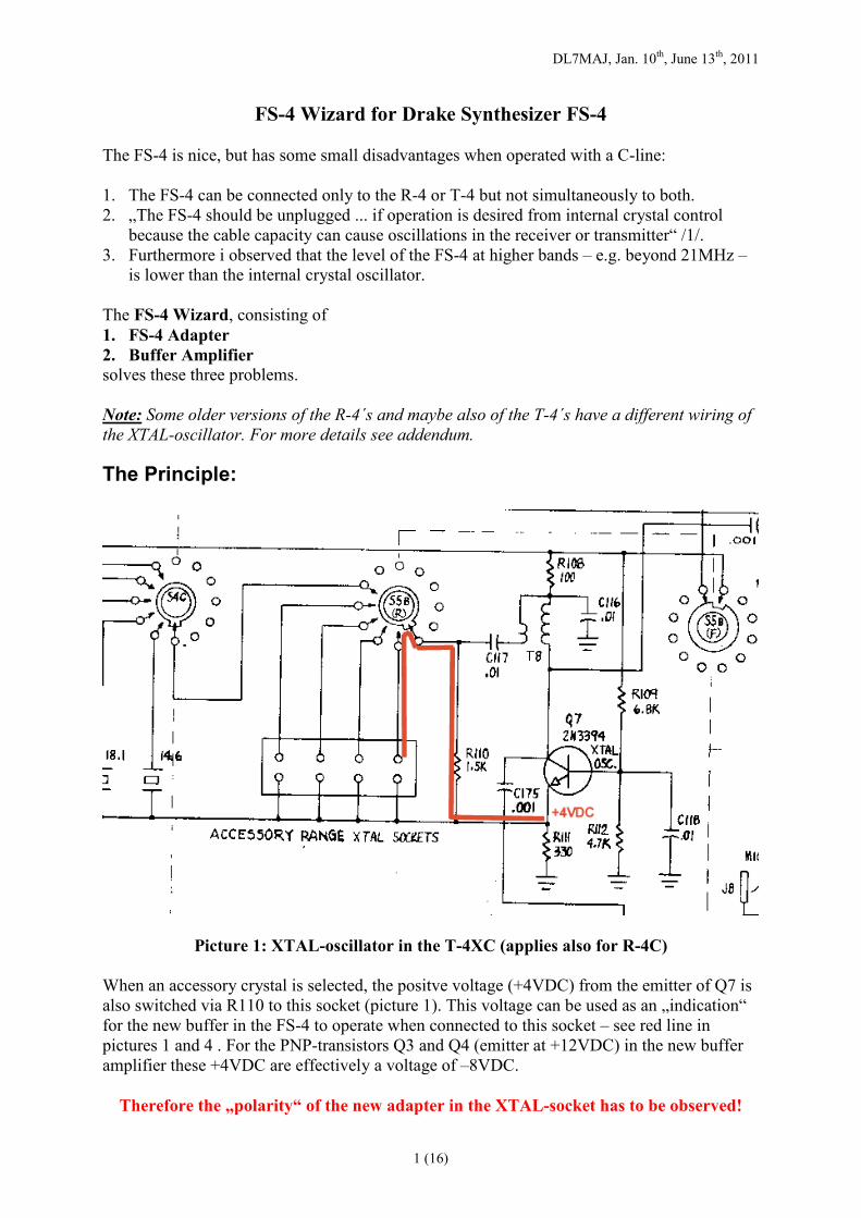
Picture 1: XTAL-oscillator in the T-4XC (applies also for R-4C)
When an accessory crystal is selected, the positve voltage (+4VDC) from the emitter of Q7 is
also switched via R110 to this socket (picture 1). This voltage can be used as an „indication“
for the new buffer in the FS-4 to operate when connected to this socket – see red line in
pictures 1 and 4 . For the PNP-transistors Q3 and Q4 (emitter at +12VDC) in the new buffer
amplifier these +4VDC are effectively a voltage of –8VDC.
Therefore the „polarity“ of the new adapter in the XTAL-socket has to be observed!

DL7MAJ, Jan. 10th, June 13
th, 2011
2 (16)
The Circuit:
1. The FS-4 Adapter
The FS-4-Adapter isolates the capacity of the coax cable from the crystal socket, so this
adapter with the cable may be left plugged in even when the FS-4 is not used!
Additionally it transfers the DC-voltage via the 100kOhm resistor from the emitter of Q7 to
the FS-4 Buffer (picture 2). OBSERVE POLARITY IN THE XTAL-SOCKET!
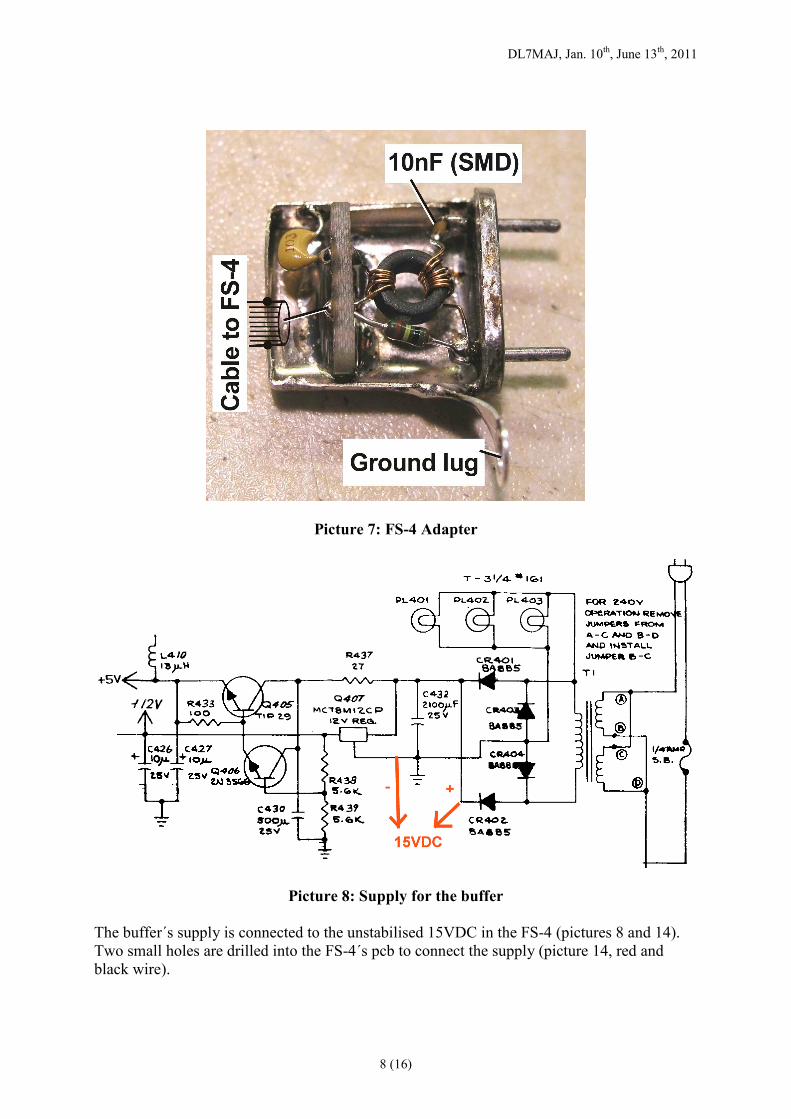
Picture 2: FS-4 Adapter
T1 is a step-up transformer to increase the voltage. Both windings are on the opposite side of
the core to minimize the capacitive coupling between. Via the resistor (100kOhms) the DC-
voltage is fed to the buffer; the two caps (one is SMD) isolate this DC against ground; see
also picture 7. I used the case of an old crystal.
2. The Buffer Amplifier
The buffer amplifier (picture 3) has two identical „channels“; the function is described for
channel „1“: The signal from the FS-4 (JP1) is separated by R1/R2 and R21/R22 from
channel 2 and fed to amplifier Q1. C1 and C2 are dimensioned for more amplification at
higher frequencies (see topic 3 above). Q2 is an emitter follower to get an low impedance
output at JP2. Q3 and Q4 get conductive when the above mentioned DC-level is fed to the
circuit via the FS4-adapter and R9/R11. LED1 indicates the „ON“-status of this output ; the
complete DC-path is shown in picture 4. The 15VDC are taken directly from the FS-4 (see
pictures 8 and 14) and stabilised by IC1.
Channel 2 (Q5/6/7/8) operates in the same way (picture 3).

DL7MAJ, Jan. 10th, June 13
th, 2011
3 (16)
Picture 3: Schematic of the buffer amplifier

DL7MAJ, Jan. 10th, June 13
th, 2011
4 (16)
Picture 4: DC-path from the emitter of Q7 (T-4XC) to the buffer amplifier (Q3/Q4)

DL7MAJ, Jan. 10th, June 13
th, 2011
5 (16)
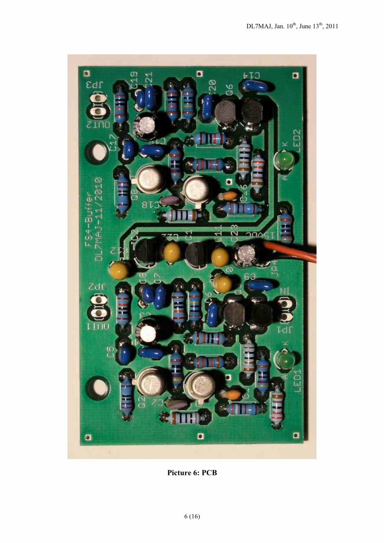
Picture 5: Layout of the buffer amplifier (74mm x 44mm)
3. Technical Data
Frequency: 11MHz to 41MHz
Gain: between JP1 and JP2 or JP3 (FS4-adapter connected)
At 11MHz: app. 1,0 / at 41MHz: app. 1,2
Supply Voltage >14VDC
Current consumption:Both channels „ON“ and both LEDs lighting: 95mA
One channel „ON“ and one LED lighting: 50mA
Both channels „OFF“ and no LEDs lighting: 5mA
Dimension: 74mm x 44mm
DL7MAJ, Jan. 10th, June 13
th, 2011
6 (16)
Picture 6: PCB

DL7MAJ, Jan. 10th, June 13
th, 2011
7 (16)
Part Value Part Value
C1 27p Q1 2N2222A
C2 100p Q2 2N2222A
C3 10u/25V Q3 BC557
C4 100n Q4 BC557
C5 1n Q5 BC557
C6 100n Q6 BC557
C7 100n Q7 2N2222A
C8 1n Q8 2N2222A
C9 100n R1 470R
C10 0,47u/25V R2 2k2
C11 0,47u/25V R3 3k9
C12 0,47u/25V R4 100R
C13 10u/25V R5 12k
C14 100n R6 470R
C15 100n R7 10k
C16 27p R8 1M
C17 1n R9 10k
C18 100p R10 270R
C19 1n R11 10k
C20 100n R12 1k
C21 100n R13 470R
C22 0,47u/25V R14 12k
C23 10u/25V R15 270R
IC1 78L12 R16 10k
IC2 78L12 R17 1M
LED1 10mA R18 10k
LED2 10mA R19 100R
R20 10kLED1 and 2 are only for indication during tests R21 470RThey can be removed – and also R12 and R23 R22 2k2
R23 1k
R24 3k9
List 1: Partslist
Picture 5,6 and list 1 show the layout and partslist.
Installation and no alignment
The buffer may be installed inside the FS-4 (pictures 14 and 15). Input, output and DC-supply
are wired on shortest ways. Only one additional hole has to be drilled on the rear side of the
FS-4 (picture 16). No alignment is necessary; also the FS-4 requires no realignment.
DL7MAJ, Jan. 10th, June 13
th, 2011
8 (16)
Picture 7: FS-4 Adapter
Picture 8: Supply for the buffer
The buffer´s supply is connected to the unstabilised 15VDC in the FS-4 (pictures 8 and 14).
Two small holes are drilled into the FS-4´s pcb to connect the supply (picture 14, red and
black wire).

DL7MAJ, Jan. 10th, June 13
th, 2011
9 (16)
Picture 9: FS-4 Adapter in the T-4XC
Picture 10: FS-4 Adapter and cabling in the T-4XC
Pictures 9 and 10 show the adapter in the T-4XC at XTAL-position 4 and the cabling.
Picture 11 shows the connection at the rear side of the T-4XC.

DL7MAJ, Jan. 10th, June 13
th, 2011
10 (16)
Picture 11: FS-4 connection at the rear side of T-4XC
Picture 12 and 13 show the other adapter at the R-4C in XTAL-position 15.
Picture 12: FS-4 Adapter at the R-4C
DL7MAJ, Jan. 10th, June 13
th, 2011
11 (16)
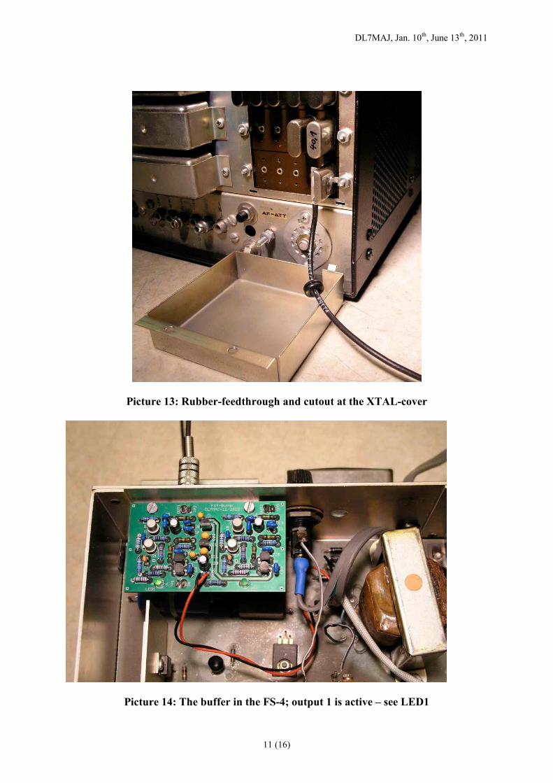
Picture 13: Rubber-feedthrough and cutout at the XTAL-cover
Picture 14: The buffer in the FS-4; output 1 is active – see LED1

DL7MAJ, Jan. 10th, June 13
th, 2011
12 (16)
Picture 15: Installation of the buffer in the FS-4
The buffer is installed with a small aluminum-profile, the two nuts are fixed with glue - see
picture 15.
Picture 16: Rear side of the FS-4, R-4C and T-4XC with cabling

DL7MAJ, Jan. 10th, June 13
th, 2011
13 (16)
HF-Isolation
When the buffer is automatically switched off, it´s output should be „zero“.
In reality there is a small capacitive coupling through the buffer and the adapter, so the output
is not absolutely zero. I measured a damping of >55 dB with my T-4XC at 10m
(29,000MHz).
Method:
1. 100% output with FS-4 operative, i.e. 48dBm (picture 17).
2. Then selecting an empty XTAL-socket in the T-4XC, so that the output should be „zero“.
No change in the T-4XC-settings! The capacitive coupling caused –7dBm output.
Note: In both pictures, the reference line (top) has +10dBm; the power attenuator had 40dB.
In practice, this would only be a problem when operating with XTAL-control in the same
band as the FS-4 operates – but this operation makes no sense.
In split operation, all selective circuits within the C-Line prevent any unwanted output or
spurii.
The only exception may be split operation within the 10m-Band. In this case, the FS-4 should
control the TX.
Picture 17: T-4XC output with FS-4 ON, tuned at 29,000MHz

DL7MAJ, Jan. 10th, June 13
th, 2011
14 (16)
Picture 18: T-4XC output with FS-4 ON, but other XTAL selected
Use of two buffers
If you have more than two 4-Line rigs (congrats!!), you can use a second buffer connected in
parallel to the first buffer; so you have totally four outputs. The input impedance of the buffer
amplifier is high enough not to overload the output of the FS-4.
This configuration should be made outside the FS-4 due to the small space inside the FS-4.

DL7MAJ, Jan. 10th, June 13
th, 2011
15 (16)
Addendum
Göran, SM7DLK reported a problem with his R-4B and his solution (picture 18).
Picture 18: XTAL-Oscillator in the R-4B
The resistor R113 (1k5) is not wired to S1 but to S5E. Therefore this resistor is active only in
the NORM-operation of the crystals. When operating the accessory crystals – or the FS-4- this
resistor is not active and therefore it can´t activate the buffer amplifier in the FS-4 wizard as
described in picture 4 (R110). Göran proposes to cut one side of R113 from S5E and add a
new resistor to S1 (wiper) as shown in picture 18 to 21 – mni tnx!
Picture 19: R-4B, cut resistor

DL7MAJ, Jan. 10th, June 13
th, 2011
16 (16)
Picture 20: R-4B, new resistor
Picture 21: T-4XB, cut resistor
Note:
I don´t know, which rigs from the 4-Line have a need for this modification. When the buffer
amplifier is not switched on/off as expected, a check of the wiring is proposed.
/1/ Instruction Manual Drake Model FS-4
If you want to contact the author:
Stefan Steger, DL7MAJ, eMail: [email protected]
Homepage: www.dl7maj.de