Embed Size (px)
Citation preview

Frontend Electronics in SOI at
FERMILAB
MAMBO III
Monolithic Active Pixel Matrix
with Binary Counters
Farah Khalid
Alpana Shenai
Gregory Deptuch
Raymond Yarema1

Presentation OutlineOverview of SOI technology
Implications of designing in SOI
Previous Work: MAMBO II
Design
Results
MAMBO III development
Goals
Schematic
Layout
ZyCube 3D Integration
MAMBO IV: Future work
2

OVERVIEW OF SOI
PROCESSES
3

Overview of SOI technologyCMOS BULK Fully / Partially depleted
4
• Substrate provides common body
potential in bulk CMOS processes (these
can be separated by well)
• Sub threshold slope n= 1.2- 1.4
• Suffers from junction capacitances and
leakages of these junctions
• Bulk may have fixed body potential thus
no threshold voltgae variation in any
dynamic states
•Bulk is sensitive to SEU but immune to TID
• For partially depleted the channel inversion
does not consume the entire body
• Sub threshold slope : 1.0
• Almost no jucntion capaciatnces
• Body potential may vary with bias
conditions as they change on all electrodes
and with transients (!), so threshold voltage
may be fluctuating thus some people may
see it as a source of extra noise
•SOI is immune to SEU but sensitive to TID

IMPLICATIONS OF DESIGNING
IN FD SOI
5

SOI Technology advantagesHigh Resistivity (Sensor) + Low Resistivity
(CMOS)
No more Latch Up (no parasitic bipolar
transistor)
Reduction of diffusion capacitance.
Source/Drain diffusion areas coupled to
BOX (εr = 4.1) instead of Si (εr = 12)
Cascoding possible due to reduced body
effect (essential for increasing gain)
Significantly reduced leakage currents6

Digital Design Advantages
Floating Body transistors speeding up
(kink effect)
Normal Voltage Kink
Increased slope of I-V plot as Vgate rises
High Voltage Kink
Elevated I-V slope during stress
Improved, higher slope for gm
Lower node capacitance,
faster switching
7

Analogue Design Issues
SOI is a 5 terminal device
Depending on the bias, transistors may
operate with fully depleted bulk or
undepleted bulk (or in between these two
conditions)
Imprecise modeling information
Noise parameters
Montecarlo parameters for process and
mismatch
Analogue Design fine tuned experimentally
during tests8

Floating body effects Threshold Variability
Body voltage alters device
threshold via Body Effect.
Body voltage is
equilibrium of rapid AC
(coupling) and slower DC
(charging/discharging)
mechanisms.
Transient body voltages
substantially differ from its
steady-state value.
9
[Kerry Bernstein, SOI Circuit Design
Considerations, EECS VLSI Seminar
Series, University of Michigan, 1 April,
2002]

Bipolar effect
If the body voltage floats up to (Vsource+Vdiode):
Junction Diode to the device’s source becomes fwd-biased
Body thinks it’s the base of an active bipolar device.
Momentary current flows from body (base) to source (emitter)
until the body-source voltage discharges below Vdiode.
Simultaneously, bipolar current flows from drain (collector) to
source (emitter).
Bipolar Gain b ranges from ~0.1 to ~5.0.10
Impact Ionisation
Junction leakage
I
βI
Sample and Hold Circuitsa transistor switch may lead to discharging of a storage
capacitance of a S/H circuit if the voltage on the
opposite side of the switch changes in such way that
the parasitic npn bipolar transistor gets switched ON
[Kerry Bernstein, SOI Circuit Design Considerations, EECS
VLSI Seminar Series, University of Michigan, 1 April, 2002]11

Self-heating effects SiO2 insulates thermally as well as electrically
(SOI MOSFET is isolated laterally by oxide, below by BOX, above
by field oxide)
Thermal conductivity of SiO2 is 100 times worse than Si
SOI circuit may have local hot spots
E.g. of the self heating problems
are current mirrors, commonly used in DACs and ADCsif one have a common branch where input current is injected and a secondary branches
with output current the power dissipation depends on voltage of drain terminals of the
branch transistors, if power changes occur close to the primary tranistor its vgs volatge
may change thus causing changes of currents in all branches!
the variations may go up to even 10%,
difficulty of achieving high resolutions DAC or ADCs in SOI
is reported12
Physically close in the layout
I
VG
VD

Matching Potentially poorer matching in SOI processes comparing
to bulk counterparts
Mismatch due to process variation
Mismatch due to dynamic bias conditions (heat, transients)
Thin layers of Si suffer from variation of thicknesses
Oxide everywhere on Si, build up of stress (changing with
temperature), straining or compressing the Si locally
affecting the carrier mobility
Oxides are conducting flow of contaminating ions, ions
may accumulate in certain areas, under Si islands
changing local electrical conditions
13

Body tie resistance variation
14
Quality of bulk contact
depends strongly on the
biasing in FDSOI and PDSOI,
if strong gate bias is present
bulk is pratically not existing
thus the resistance is very
high
The path of biasing of bulk is
usually pinched – naturally
high resitance

H – gate transistors
H-gate or half h-gate are not OK, source inserted contact would be prefered.
Poor quality of transistor bulk contacts,
even using so called H-gate transistors;
due to charge accumulation in oxide
bulk is floating
The biasing of bulk in H-gate is not well
controlled by any means available in the
design; with receiving TID dose the
quality of body contact may gradually
deteriorate

H – gate transistors
Box charging
Bulk contacts are in MΩ instead of kΩ due to
temporarily charged bulk
Especially in NMOS the positive charge in BOX
may completely cut bulk biasing under the
extension of the H-gate gate
16
Source- tie transistor, an alternative to
the H-gate transistor
• Decreased Overall size for
same W/L
• Decreased parasitic, gate to
drain capacitance
• Asymmetrical structure

Bibliography & further reading…. Kerry Bernstein, SOI Circuit Design Considerations, EECS VLSI Seminar Series,
University of Michigan, 1 April, 2002
K. Bernstein and N.J. Rohrer, SOI Circuit Design Concepts, Kluwer Academic
Publishers; ISBN: 0792377621, February, 2000
Proceedings, 1999 IEEE International Solid-State Circuits Conference, Session 25,
pp. 424-439
C F Edwards, W Redman-White, B M Tenbroek, M S L Lee and M J Uren, “The
Effect of Body Contact Series Resistance on SOI CMOS Amplifier stages”, IEEE
Trans on Electron Devices, Vol 44, No 12, pp. 2290-2294, Dec 1997
B M Tenbroek, W Redman-White, M S L Lee, R J T Bunyan, and M J Uren, "Impact
of self-heating and thermal coupling on analog circuits in SOI CMOS" IEEE Journal of
Solid State Circuits, Vol 33, No 5, pp1037-1046, May 1998
17

PREVIOUS WORK
18

Possible applications
E.g.
X-ray autoradiography
Fluorescence X-ray spectroscopy
Low energy applications up to 12kEv
19

Ch
Design details of pixel imaging detector „MAMBO”
MAMBO = Monolithic Active Pixel Matrix with Binary Counters
• each pixel:
integrating CSA w/ p-z network,
shaping filter CR-RC2 with
tp=200ns; gain=~200 mV/e- for
small Q, multiple diodes/pixel,
ripple counter reconfigurable
into shift register
• compact design excluding use of physical resistors
Cc=28 fF, Cfs=3.3 fF, Rfs=50 MW, Gm=5.8 mS, Ch=30 fF,
MAMBO II architecture
MAMBO2: PREVIOUS WORK….
20

Design details of pixel imaging detector „MAMBO”
47m
m
47 mm MAMBO II pixel layout
Single pixel test structure is a fully functional
ciruit allowing monitoring: shaper output,
discriminator output, counter output
Multiple p-taps (used as signal electrodes) present per
pixel for reduction of shifts of threshold voltages.
Partial success: adjustment of bias voltages and
currents (referred to VGS) up to several tens of mV still
required for Vback from the range from 0 to 10V.
MAMBO II chip layout
single pixel
test
structrue
13 diodes
in parallel
connection
94×94
pixels
array
8×10 20×20 mm2 3T pixel matrices for
x-talk and test charge collection tests
MAMBO2: PREVIOUS WORK….
21

Achievements, observations and investigations
MAMBO II single pixel test
Monitoring of the shaper and discriminator outputs (transient signals )
55Fe 109Cd
22

• the OKI process offers enhancements: through BOX contacts and diode and ohmic
implants in the substrate material for the first time in a commercial approach!
L
J
K• matrices using 3T-type pixels can succesfully be built (NMOS/PMOS switches may
be used); – some progress but not too much beyond bulk MAPS.
• mutual influence of CMOS circuitry and the detector is affecting designs of more
advanced circuits for imaging.
credo: strength of the SOI monolithic active pixel technology is integration of
whole processing circuitry directly into ‘the focal plane’
• FD-SOI represents challenges for precise analog circuits, one would prefer different
flavor!
• the properties of the substrate material and how it is depleted is far from being
understood. The depletion may depend on transient and statically hold voltage states
in the CMOS circuitry!
• observed high sensitivity to irradiation; overnight exposure under 100 mCi 109Cd
under full operation causes ~100 mV voltage levels shifts.
• the process must be enhanced.
The first priorities are to separate substrate and CMOS circuitry
Conclusions
23
• monolithic detector structures can operate depleted for the first time succesfully!
J
L

MAMBO III
24

GoalsR&D
Detector and electronics on different layers (to avoid coupling)
Diodes with PPLUS with BPW to reduce leakage
Diode of the same size as the pixel to obtain parallel electric field in active volume, and avoid potential pockets
Shielding on detector layer
Possibility of changing gated diode voltage to enhance performance of the diode
Explore 3D IC technology with ZyCube
25

3D : MAMBO 3
Tier 1 contains only diodes and shielding metal MAMBO 3
bottom
ASIC
MAMBO 3
top ASIC
26

Top ASIC: PIXEL Design
PREAMP SHAPER BLR WINDOW
COMPARATOR
4b DAC H
4b DAC L
DDL Logic
COUNTER/
SHIFT
REGISTER
12b
ANALOG
BUFFER
DIGITAL
BUFFER
VthH
VthL Baseline
PREVIOUS
PIXEL
NEXT
PIXEL
Test
Output
Configuration Register -DAC setup (8bits) -Test setup (3bits)
NEXT
PIXEL
PREVIOUS
PIXEL
27

Preamplifier
Cfs=5fF, Gm=6.5µS, Rfs=28MΩ, Cc=35fF, Ch=25fF
• Protection diode at Input
• Regulated Cascode: to increase gain
•Leakage current compensation
• 1.7fF I/P test capacitance
28
DMOS
nvt
lvt

Shaper and Baseline Restorer
BASELINE RESTORER29
• Current scaled down by 4 in the shaper, transistors scaled to maintain equal DC
volatges in the inputs, this is essentail for matching preamplifier and shaper circuits.
• High value feedback resitsance achieved with an active transistor with constant vgs.
• AC coupling to baseline restorer.

Analog Test Buffer
SOURCE FOLLOWER
SOURCE FOLLOWER
•Source
Followers
using Zero Vt
DMOS
transistor
• Single Stage
amplifier
•Disconnected
during normal
mode of
operation
•10 µA current
30
Spying all pixels one by one and gather statistical information
on the performance of pixels directly in vivo, in the matrix, this
was not available in Mambo II.
We will be able to gather staitstical information about offsets for
this process
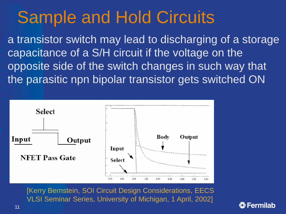
Comparator
• Hysteresis Comparator
• Connected to Vref during normal operation
OR
•Connected to baseline for trimming
OR
•Connected to gnd! When disabled
31

Window Comparator
VthL – Lower
Threshold
VthH –Upper
Threshold
VthL < Signals < VthH
is recorded as HIT
Comparators are
independently
trimmed to cancel
offsets
32

Double Discriminator Logic
• Output of the Lower Threshold
comparator behaves as a clock
• Output of the Upper Threshold
comparator behaves as a Reset
• When both comparators fire the
hit is not counted
33

Current Steering DAC (4 bits)
M = 1 M = 2 M = 4 M = 8
• Binary weighted current mirrors
• Switches are also binary weighted
• Current can be steered either to positive or negative output
34

DAC Layout
4 3 4 3 4
4 2 1 2 4
4 3 4 3 4
Conventional symmetrical common
centroid geometry for current mirrors
Helps to average out global errors
Matching is critical for monotonic
performance
35

Trimming DACs
Offset distribution after digital compensation
Offset distribution before compensation
•Gaussian distribution
•Depends on component matching
• Uniform distribution
• Residual offset depends on DAC resolution
Matching is expected to be worse for SOI, Data corresponds to a typical bulk CMOS
36

Configuration RegisterSerial In Parallel Load
(4b x 2) for DAC settings
3 bit test setup
Test Control block used as decoder to control switches for test
FlipFlop2Q
CD
FlipFlop1Q
CD
FlipFlop11Q
CD
Latch2Q
CD
Latch11Q
CD
Latch1Q
CD
Serial Clk
Parallel Load
Setup
000 Normal Operation
001 Analogue Output for test calibration
010 Test Input, counter connected
011 Calibrate DAC L
100 Calibrate DAC H
101 xx
110 xx
111 Pixel Disabled37

Counter /Shift Register
12 bit ripple counter
Count switch disconnects counter from comparator while shifting
CK_READ is external clock used for shifting data
Shift switch applied shifting clock
38
s1 and s2 are non-
overlapping clocks
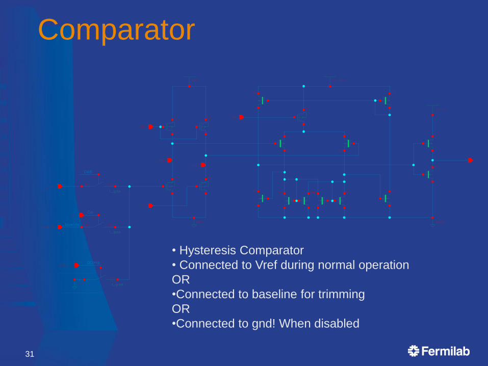
Simulation result
PREAMP INPUT
PREAMP OUTPUT
SHAPER OUTPUT
Comparator : Lower Threshold
Comparator : Upper Threshold
DDL Output
39

LAYOUT
40

MAMBO3: top pixel
• 100µ x 100µm
•Transistor count ~ 950
Co
nfi
gu
rati
on
Re
gis
ter
DACs
Test
Control
Logic
Double
Discriminator
Logic
Comparators
Shaper
Preamplifier
Analogue
Buffer
Co
un
ter / S
hift R
eg
iste
r
Dig
ital B
uffe
r
41

Upper Chip
• 5mm x 5mm
• 1936 pixel matrix (44
x44)
• Each column has
additional buffering of
analog and digital
signals
• Pads with back metal
opening
• Alignment markers
on all 4 corners
42

Lower chip: Diode Pixel
DIODE
100µ x
100µ43

Lower Chip
• 5mm x 5mm
• 1936 pixel matrix (44 x44)
• 4 guard rings around the
matrix
• No bond Pads contains only
micro bump pads, aligned
with the top chip.
• Alignment markers on all 4
corners
44

Chip connectionMICROBUMP (5µmx5µm)
-Diode connection per
pixel
-Dummy connections
-guard rings
-diode shielding (gnd!)
-gate control45

Protection
Shielding per pixel using back metal
• After handle wafer is
removed the bodies of
transistors and sensitive
nodes are exposed to
electrical coupling from
external environment
•Backplane connected to
Analogue Ground per pixel
•Peripheral digital logic
connected to Digital ground
plane exposed transistor
46
BMetal
Slot in BMetal

INTEGRATION
47

ZyCube 3D Integration process
48

3D Model
49
3D Model: Diode
50

MAMBO IV: FUTURE WORK
51

Back to 2D Availability of nested
well option
BNW layer inside a
deeper BPW implant
Isolation of diode and
electronics
Increased parasitic
junction capacitance
(currently undetermined)
52
BPW
BNW
MAMBO IV
53

MAMBO IV
54


![Frontend Electronics in SOI at FERMILAB MAMBO III · [Kerry Bernstein, SOI Circuit Design Considerations, EECS VLSI Seminar Series, University of Michigan, 1 April, 2002] Bipolar](https://img.dokumen.tips/doc/110x75/5e4afee93496154c4941c14f/frontend-electronics-in-soi-at-fermilab-mambo-iii-kerry-bernstein-soi-circuit.jpg)