Embed Size (px)
Citation preview
Nuclear Instruments and Methods in Physics Research A 567 (2006) 264–267
Front-end electronics for PWO-based PHOS calorimeter of ALICE
Hans Mullera,�, Dmitry Budnikovd, Mikhail Ippolitovc, Qingxia Lie, Vladislav Mankoc,Rui Pimentaa, Dieter Rohrichf, Iouri Sibiryakc, Bernhard Skaalib, Alexandre Vinogradovc
aCERN, Division PH, Geneva, SwitzerlandbDepartment of Physics, University of Oslo, Norway
cKurchatov Institute, Moscow, RussiadRFNC VNIIEF, Sarov, Russia
eHuazhong University of Science and Technology, Wuhan, PR ChinafDepartment of Physics, University of Bergen, Norway
Available online 12 June 2006
Abstract
The electromagnetic Photon Spectrometer (PHOS) of ALICE consists of five modules with 56� 64 PWO crystals, operated at �25 1C.
Glued to each crystal are APD diodes which amplify a lightyield of 4.4 photoelectrons/MeV, followed by charge-sensitive pre-amplifiers
with a charge conversion gain of ca. 1V/pC. We describe our new 32-channel shaper/digitizer and readout electronics for gain-
programmable photodiodes. These Front-End Electronics (FEE) cards are installed below the crystals in an isolated warm volume in
geometrical correspondence to 2� 16 crystal rows per card. With a total detector capacitance of 100 pF and a noise level of 3MeV, the
FEEs cover a 14 bit dynamic range from 5MeV to 80GeV. The low noise level is achieved by operating the APDs and preamplifiers at
low temperature and by applying a relatively long shaping time of 1ms. The offline timing resolution, obtained via a Gamma-2 fit is less
than 2 ns. The second-order, dual-gain shapers produce semi-Gaussian output for 10 bit ADCs with embedded multi-event buffers. A
Readout Control Unit (RCU) masters data readout with address-mapped access to the event-buffers and controls registers via a custom
bus which interconnects up to 14 FEE cards. Programmable bias voltage controllers on the FEE cards allow for very precise gain
adjustment of each individual APD. Being co-designed with the TRU trigger cards, each FEE card generates eight fast signal sums (2� 2
crystals) as input to the TRU. FPGA-based algorithms generate level-0 and level-1 trigger decisions at 40MHz and allow PHOS also to
operate in self-triggered mode. Inside each PHOS module there are 112 FEE and 8 TRU cards which dissipate ca. 1 kW heat which is
extracted via a water cooling system.
r 2006 Elsevier B.V. All rights reserved.
PACS: 42.66.Lc; 85.60.Dw; 85.60.Gz; 29.40.Vj
Keywords: Electromagnetic calorimeter; PWO; APD; FEE electronics; RMS noise; Shaping time; Energy resolution; Timing resolution; Fast-OR;
Embedded electronics packaging; Trigger-electronics; APD gain calibration
1. PHOS calorimeter
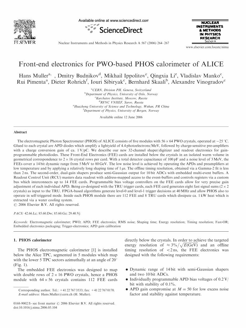
The PHOS electromagnetic calorimeter [1] is installedbelow the Alice TPC, segmented in 5 modules which mapwith the lower 5 TPC sectors azimuthally at an angle of 201(Fig. 1).
The embedded FEE electronics was designed to mapwith double rows of 2� 16 PWO crystals, hence a PHOSmodule with 64� 56 crystals contains 112 FEE cards
directly below the crystals. In order to achieve the targetedenergy resolution of � 3%
� ffiffiffiffiffiffiffiffiffiffiffiffiffiffiffiffiffiEðGeVÞ
pand an offline
timing resolution of o2 ns, the FEE electronics wasdesigned with the following requirements:
� Dynamic range of 14 bit with semi-Gaussian shapersand two 10 bit ADCs.� Individually programmable APD bias voltages of 0.2V/
bit with stability of 0.1%.� APD gain compromise at M ¼ 50 for low excess noise
factor and stability against temperature.
ARTICLE IN PRESS
www.elsevier.com/locate/nima
0168-9002/$ - see front matter r 2006 Elsevier B.V. All rights reserved.
doi:10.1016/j.nima.2006.05.104
�Corresponding author. Tel.: +4122 767 3533; fax: +41 22 767 0170.
E-mail address: [email protected] (H. Muller).
� Detector dark noise of 3MeV (700 electrons) perchannel, resulting in a 3� 3 shower noise term of ca.9MeV.� Dual gain shapers of gain ratio 1/16 for a 14 bit dynamic
range between 5MeV and 80GeV.� Second-order Bessel filter for linear transfer character-
istics, low noise and Gamma-2 pulse-shape of the form
V2ndðtÞ ¼4QA2
Cf
� �t
tp
� �2e�2t=tp .
� Analogue sum output of 2� 2 cells in the range8MeV–33GeV for the TRU trigger module.
2. PHOS electronics
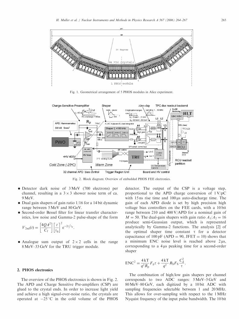
The overview of the PHOS electronics is shown in Fig. 2.The APD and Charge Sensitive Pre-amplifiers (CSP) areglued to the crystal ends. In order to increase light yieldand achieve a high signal-over-noise ratio, the crystals areoperated at �25 1C in the cold volume of the PHOS
detector. The output of the CSP is a voltage step,proportional to the APD charge conversion of 1V/pCwith 15 ns rise time and 100 ms auto-discharge time. Thegain of each APD diode is set by high precision highvoltage bias controllers on the FEE cards, with a 10 bitrange between 210 and 400V/APD for a nominal gain ofM ¼ 50. The dual-gain shapers with gain ratio A1/A2 ¼ 16produce semi-Gaussian output, which is representedanalytically by Gamma-2 functions. The analysis [2] ofthe optimal shaper time constant t for a detectorcapacitance of 100 pF (APD ¼ 90, JFET ¼ 10) shows thata minimum ENC noise level is reached above 2 ms,corresponding to a 4 ms peaking time for a second-ordershaper
ENC2¼
4 kT
q2RpFptþ
4 kT
q2RSFS
C2d
t.
The combination of high/low gain shapers per channelcorresponds to two ADC ranges: 5MeV–5GeV and80MeV–80GeV, each digitized by a 10bit ADC withsampling frequencies selectable between 1 and 20MHz.This allows for over-sampling with respect to the 1MHzNyquist frequency of the input pulse bandwidth. The 10bit
ARTICLE IN PRESS
Fig. 1. Geometrical arrangement of 5 PHOS modules in Alice experiment.
Fig. 2. Block diagram: Overview of embedded PHOS FEE electronics.
H. Muller et al. / Nuclear Instruments and Methods in Physics Research A 567 (2006) 264–267 265
digitizers are Altro-16 chips [3] with 16 channels of ADC’sfollowed by Multi-event Buffers (MEB). The latter allowsfor pipelined event buffering and block readout undercontrol of two external trigger signals. The common readoutbus of the FEE and TRU cards is mastered by an externalReadout Control Unit (RCU) which reads events from allMEBs whenever a level-0 and level-2 trigger sequence isreceived. From the event-buffer on the RCU, events aretransferred via the 200Mbit/s optical data link to the Localand Global Data Concentrators (LDC/GDC) of the DAQsystem and to the High level trigger farm (HLT).
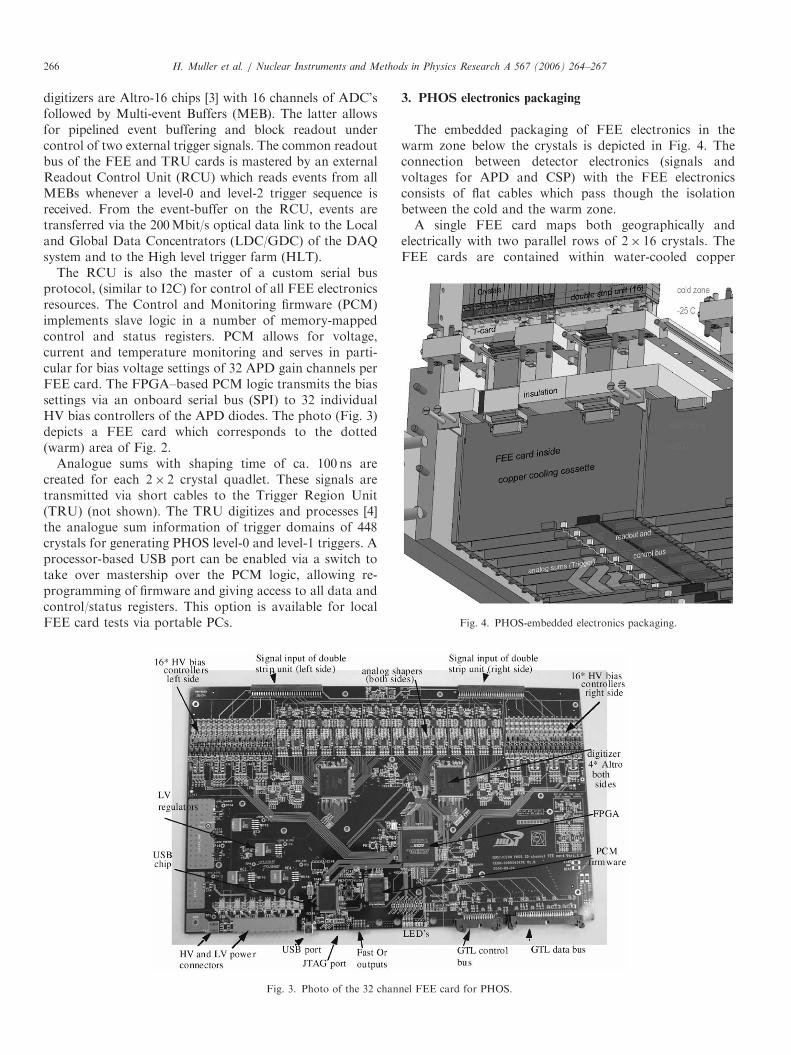
The RCU is also the master of a custom serial busprotocol, (similar to I2C) for control of all FEE electronicsresources. The Control and Monitoring firmware (PCM)implements slave logic in a number of memory-mappedcontrol and status registers. PCM allows for voltage,current and temperature monitoring and serves in parti-cular for bias voltage settings of 32 APD gain channels perFEE card. The FPGA–based PCM logic transmits the biassettings via an onboard serial bus (SPI) to 32 individualHV bias controllers of the APD diodes. The photo (Fig. 3)depicts a FEE card which corresponds to the dotted(warm) area of Fig. 2.
Analogue sums with shaping time of ca. 100 ns arecreated for each 2� 2 crystal quadlet. These signals aretransmitted via short cables to the Trigger Region Unit(TRU) (not shown). The TRU digitizes and processes [4]the analogue sum information of trigger domains of 448crystals for generating PHOS level-0 and level-1 triggers. Aprocessor-based USB port can be enabled via a switch totake over mastership over the PCM logic, allowing re-programming of firmware and giving access to all data andcontrol/status registers. This option is available for localFEE card tests via portable PCs.
3. PHOS electronics packaging
The embedded packaging of FEE electronics in thewarm zone below the crystals is depicted in Fig. 4. Theconnection between detector electronics (signals andvoltages for APD and CSP) with the FEE electronicsconsists of flat cables which pass though the isolationbetween the cold and the warm zone.A single FEE card maps both geographically and
electrically with two parallel rows of 2� 16 crystals. TheFEE cards are contained within water-cooled copper
ARTICLE IN PRESS
Fig. 3. Photo of the 32 channel FEE card for PHOS.
Fig. 4. PHOS-embedded electronics packaging.
H. Muller et al. / Nuclear Instruments and Methods in Physics Research A 567 (2006) 264–267266
cassettes which are open to the bottom for connectingpower, readout and control buses and analogue sums forthe TRU cards which are inserted in the middle between2� 7 FEE cards.
4. Results
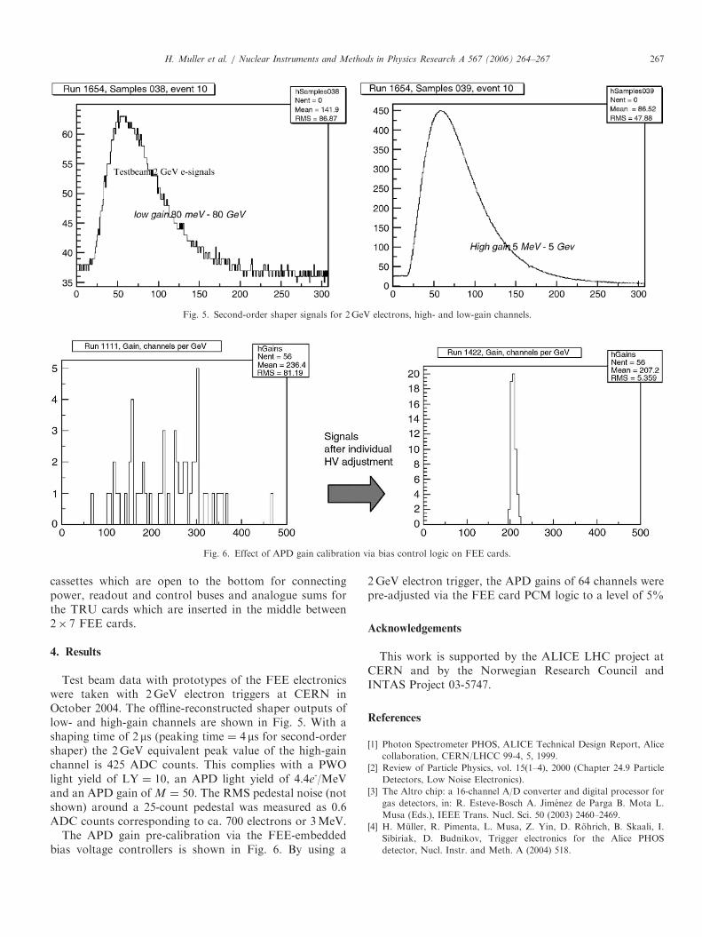
Test beam data with prototypes of the FEE electronicswere taken with 2GeV electron triggers at CERN inOctober 2004. The offline-reconstructed shaper outputs oflow- and high-gain channels are shown in Fig. 5. With ashaping time of 2 ms (peaking time ¼ 4 ms for second-ordershaper) the 2GeV equivalent peak value of the high-gainchannel is 425 ADC counts. This complies with a PWOlight yield of LY ¼ 10, an APD light yield of 4.4e-/MeVand an APD gain of M ¼ 50. The RMS pedestal noise (notshown) around a 25-count pedestal was measured as 0.6ADC counts corresponding to ca. 700 electrons or 3MeV.
The APD gain pre-calibration via the FEE-embeddedbias voltage controllers is shown in Fig. 6. By using a
2GeV electron trigger, the APD gains of 64 channels werepre-adjusted via the FEE card PCM logic to a level of 5%
Acknowledgements
This work is supported by the ALICE LHC project atCERN and by the Norwegian Research Council andINTAS Project 03-5747.
References
[1] Photon Spectrometer PHOS, ALICE Technical Design Report, Alice
collaboration, CERN/LHCC 99-4, 5, 1999.
[2] Review of Particle Physics, vol. 15(1–4), 2000 (Chapter 24.9 Particle
Detectors, Low Noise Electronics).
[3] The Altro chip: a 16-channel A/D converter and digital processor for
gas detectors, in: R. Esteve-Bosch A. Jimenez de Parga B. Mota L.
Musa (Eds.), IEEE Trans. Nucl. Sci. 50 (2003) 2460–2469.
[4] H. Muller, R. Pimenta, L. Musa, Z. Yin, D. Rohrich, B. Skaali, I.
Sibiriak, D. Budnikov, Trigger electronics for the Alice PHOS
detector, Nucl. Instr. and Meth. A (2004) 518.
ARTICLE IN PRESS
Fig. 5. Second-order shaper signals for 2GeV electrons, high- and low-gain channels.
Fig. 6. Effect of APD gain calibration via bias control logic on FEE cards.
H. Muller et al. / Nuclear Instruments and Methods in Physics Research A 567 (2006) 264–267 267