Embed Size (px)
Citation preview

Appears in the Proceedings of the 49th Annual IEEE/ACM International Symposium on Microarchitecture, 2016
From High-Level Deep Neural Models to FPGAsHardik Sharma Jongse Park Divya Mahajan Emmanuel Amaro
Joon Kyung Kim Chenkai Shao Asit Mishra† Hadi EsmaeilzadehAlternative Computing Technologies (ACT) Lab
School of Computer Science, Georgia Institute of Technology †Intel Corporation{hsharma, jspark, divya mahajan, amaro, jkkim, cshao}@gatech.edu [email protected] [email protected]
ABSTRACTDeep Neural Networks (DNNs) are compute-intensive learningmodels with growing applicability in a wide range of domains.FPGAs are an attractive choice for DNNs since they offer aprogrammable substrate for acceleration and are becomingavailable across different market segments. However, obtainingboth performance and energy efficiency with FPGAs is alaborious task even for expert hardware designers. Furthermore,the large memory footprint of DNNs, coupled with the FPGAs’limited on-chip storage makes DNN acceleration using FPGAsmore challenging. This work tackles these challenges bydevising DNNWEAVER, a framework that automaticallygenerates a synthesizable accelerator for a given (DNN, FPGA)pair from a high-level specification in Caffe [1]. To achieve largebenefits while preserving automation, DNNWEAVER generatesaccelerators using hand-optimized design templates. First,DNNWEAVER translates a given high-level DNN specification toits novel ISA that represents a macro dataflow graph of the DNN.The DNNWEAVER compiler is equipped with our optimizationalgorithm that tiles, schedules, and batches DNN operations tomaximize data reuse and best utilize target FPGA’s memory andother resources. The final result is a custom synthesizable accel-erator that best matches the needs of the DNN while providinghigh performance and efficiency gains for the target FPGA.
We use DNNWEAVER to generate accelerators for a set ofeight different DNN models and three different FPGAs, Xil-
inx Zynq, Altera Stratix V, and Altera Arria 10. We use hardwaremeasurements to compare the generated accelerators to both mul-ticore CPUs (ARM Cortex A15 and Xeon E3) and many-core GPUs(Tegra K1, GTX 650Ti, and Tesla K40). In comparison, the gen-erated accelerators deliver superior performance and efficiencywithout requiring the programmers to participate in the arduoustask of hardware design.
1 IntroductionDeep Neural Networks (DNNs) are rapidly gaining tractionin a wide range of applications such as vision, robotics, videoanalytics, speech recognition, natural language processing,targeted advertising, and web search [2–9]. Although DNNsoffer great prediction accuracy, they require a significant amountof computing power. With diminishing benefits from technologyscaling [10, 11], the research community is increasingly turningto specialized accelerators for deep networks [12–15] and otherworkloads [16–22]. Even though ASICs provide significantgains in performance and efficiency for DNNs [12, 13, 23–26],they may not cope with the ever-evolving DNN models.Furthermore, ASICs and customized cores come at the priceof high non-recurring engineering costs over long design periods.Since FPGAs represent an intermediate point between theefficiency of ASICs and the programmability of general purposeprocessors, they are an attractive alternative for accelerating
DNNs. Nonetheless, FPGAs still require extensive hardwaredesign expertise and long design cycles. In fact, several researchworks [14, 15, 27, 28] have made extensive efforts to provideFPGA accelerators for specific DNN models, or parts of DNNcomputation, targeted for a particular FPGA platform.
Using FPGAs as an acceleration platform for DNNs is chal-lenging as they offer a limited preset on-chip memory and oftenpossess limited off-chip bandwidth, both of which are critical forhigh performance. This restriction is particularly limiting for FP-GAs since ASIC designs can circumvent this issue by optimallyallocating die area to on-chip memory for a single or set of targetDNNs. The FPGA’s memory and bandwidth limitations arefurther exacerbated for DNNs due to their high memory footprint,as well as high variability in the number of operations and modelsizes for different DNN models (Section 7.1). A rigid acceleratorarchitecture for DNNs may not fully utilize the FPGA’s limitedresources for every DNN model. It is thus essential co-optimizeboth the accelerator architecture and the corresponding executionschedule to overcome the FPGA’s limited on-chip memory foreach DNN model. This work seeks to provide such a solutionby developing DNNWEAVER, a framework that generatessynthesizable accelerators for a variety of FPGA platforms,while completely disengaging the programmers from hardwaredesign. DNNWEAVER provides a comprehensive and automatedsolution to make FPGAs available to a broader community ofDNN application developers who use a wide range of DNNmodels and often lack any hardware design expertise.
This paper makes the following contributions to enable FPGAacceleration for a variety of DNNs:(1) We develop a novel macro dataflow Instruction SetArchitecture (ISA) for DNN accelerators. The ISA enablesDNNWEAVER to expose a high-level programming interface.The programming interface is the same as Berkeley Caffe [1].
(2) Instead of just designing an accelerator for DNNs, wedevelop hand-optimized template designs that are scalableand highly customizable. The templates constitute a clusteredhierarchical architecture that is contracted or expanded byDNNWEAVER to generate an accelerator that matches theneeds of the DNN and the available resources on the FPGA.
(3) We provide a heuristic algorithm to co-optimize both theaccelerator architecture and the corresponding executionschedule to minimize off-chip memory accesses and maximizeperformance. This algorithm strikes a balance between paralleloperations and data reuse by slicing the computation and config-uring the accelerator to best match the constraints of the FPGA.
Matching computation slice with the configuration of theaccelerator is a unique challenge that needs to be addressed tocreate a framework that can generate highly efficient FPGAaccelerators for DNNs. The aforementioned contributions enableDNNWEAVER to exploit the reconfigurability of the FPGAswhile managing the large memory footprint of DNNs in the
Xeon E3Tegra K1
GTX 650Ti
Tesla K40
Stratix V
Arria 10
0⨉
40⨉
80⨉
120⨉
160⨉
0 20 40 60 80 100 120 140
Spee
dup
/ AR
M A
15
Power (Watt)
FPGA CPU GPU
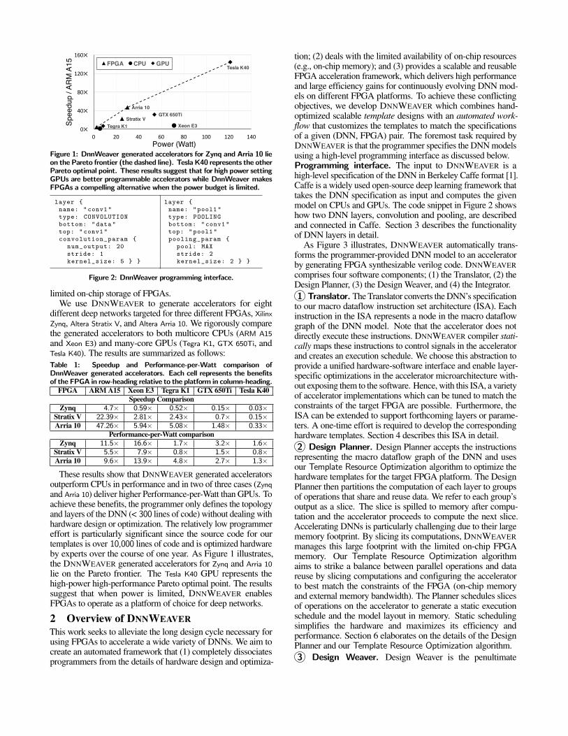
Figure 1: DnnWeaver generated accelerators for Zynq and Arria 10 lieon the Pareto frontier (the dashed line). Tesla K40 represents the otherPareto optimal point. These results suggest that for high power settingGPUs are better programmable accelerators while DnnWeaver makesFPGAs a compelling alternative when the power budget is limited.
layer {name: "conv1"type: CONVOLUTIONbottom: "data"top: "conv1"convolution_param {
num_output: 20stride: 1kernel_size: 5 } }
layer {name: "pool1"type: POOLINGbottom: "conv1"top: "pool1"pooling_param {
pool: MAXstride: 2kernel_size: 2 } }
Figure 2: DnnWeaver programming interface.
limited on-chip storage of FPGAs.We use DNNWEAVER to generate accelerators for eight
different deep networks targeted for three different FPGAs, XilinxZynq, Altera Stratix V, and Altera Arria 10. We rigorously comparethe generated accelerators to both multicore CPUs (ARM A15
and Xeon E3) and many-core GPUs (Tegra K1, GTX 650Ti, andTesla K40). The results are summarized as follows:Table 1: Speedup and Performance-per-Watt comparison ofDnnWeaver generated accelerators. Each cell represents the benefitsof the FPGA in row-heading relative to the platform in column-heading.
FPGA ARM A15 Xeon E3 Tegra K1 GTX 650Ti Tesla K40Speedup Comparison
Zynq 4.7× 0.59× 0.52× 0.15× 0.03×Stratix V 22.39× 2.81× 2.43× 0.7× 0.15×Arria 10 47.26× 5.94× 5.08× 1.48× 0.33×
Performance-per-Watt comparisonZynq 11.5× 16.6× 1.7× 3.2× 1.6×
Stratix V 5.5× 7.9× 0.8× 1.5× 0.8×Arria 10 9.6× 13.9× 4.8× 2.7× 1.3×
These results show that DNNWEAVER generated acceleratorsoutperform CPUs in performance and in two of three cases (Zynqand Arria 10) deliver higher Performance-per-Watt than GPUs. Toachieve these benefits, the programmer only defines the topologyand layers of the DNN (< 300 lines of code) without dealing withhardware design or optimization. The relatively low programmereffort is particularly significant since the source code for ourtemplates is over 10,000 lines of code and is optimized hardwareby experts over the course of one year. As Figure 1 illustrates,the DNNWEAVER generated accelerators for Zynq and Arria 10
lie on the Pareto frontier. The Tesla K40 GPU represents thehigh-power high-performance Pareto optimal point. The resultssuggest that when power is limited, DNNWEAVER enablesFPGAs to operate as a platform of choice for deep networks.
2 Overview of DNNWEAVERThis work seeks to alleviate the long design cycle necessary forusing FPGAs to accelerate a wide variety of DNNs. We aim tocreate an automated framework that (1) completely dissociatesprogrammers from the details of hardware design and optimiza-
tion; (2) deals with the limited availability of on-chip resources(e.g., on-chip memory); and (3) provides a scalable and reusableFPGA acceleration framework, which delivers high performanceand large efficiency gains for continuously evolving DNN mod-els on different FPGA platforms. To achieve these conflictingobjectives, we develop DNNWEAVER which combines hand-optimized scalable template designs with an automated work-flow that customizes the templates to match the specificationsof a given (DNN, FPGA) pair. The foremost task required byDNNWEAVER is that the programmer specifies the DNN modelsusing a high-level programming interface as discussed below.Programming interface. The input to DNNWEAVER is ahigh-level specification of the DNN in Berkeley Caffe format [1].Caffe is a widely used open-source deep learning framework thattakes the DNN specification as input and computes the givenmodel on CPUs and GPUs. The code snippet in Figure 2 showshow two DNN layers, convolution and pooling, are describedand connected in Caffe. Section 3 describes the functionalityof DNN layers in detail.
As Figure 3 illustrates, DNNWEAVER automatically trans-forms the programmer-provided DNN model to an acceleratorby generating FPGA synthesizable verilog code. DNNWEAVERcomprises four software components; (1) the Translator, (2) theDesign Planner, (3) the Design Weaver, and (4) the Integrator.1 Translator. The Translator converts the DNN’s specification
to our macro dataflow instruction set architecture (ISA). Eachinstruction in the ISA represents a node in the macro dataflowgraph of the DNN model. Note that the accelerator does notdirectly execute these instructions. DNNWEAVER compiler stati-cally maps these instructions to control signals in the acceleratorand creates an execution schedule. We choose this abstraction toprovide a unified hardware-software interface and enable layer-specific optimizations in the accelerator microarchitecture with-out exposing them to the software. Hence, with this ISA, a varietyof accelerator implementations which can be tuned to match theconstraints of the target FPGA are possible. Furthermore, theISA can be extended to support forthcoming layers or parame-ters. A one-time effort is required to develop the correspondinghardware templates. Section 4 describes this ISA in detail.2 Design Planner. Design Planner accepts the instructions
representing the macro dataflow graph of the DNN and usesour Template Resource Optimization algorithm to optimize thehardware templates for the target FPGA platform. The DesignPlanner then partitions the computation of each layer to groupsof operations that share and reuse data. We refer to each group’soutput as a slice. The slice is spilled to memory after compu-tation and the accelerator proceeds to compute the next slice.Accelerating DNNs is particularly challenging due to their largememory footprint. By slicing its computations, DNNWEAVERmanages this large footprint with the limited on-chip FPGAmemory. Our Template Resource Optimization algorithmaims to strike a balance between parallel operations and datareuse by slicing computations and configuring the acceleratorto best match the constraints of the FPGA (on-chip memoryand external memory bandwidth). The Planner schedules slicesof operations on the accelerator to generate a static executionschedule and the model layout in memory. Static schedulingsimplifies the hardware and maximizes its efficiency andperformance. Section 6 elaborates on the details of the DesignPlanner and our Template Resource Optimization algorithm.3 Design Weaver. Design Weaver is the penultimate

Design Planner
High-LevelDNN
SpecificationTranslator
Macro Dataflow Graph
Design Weaver
Accelerator Core Design Integrator Synthesizable
Accelerator
FPGA
MemoryBerkeley Caffe Weaver ISA
Hand-Optimized Templates
VerilogWeaver ParametersFPGA
Specification
Verilog
Verilog21 3 4
Memory Interface
DNN Model Layout
Execution Schedule
Resource Allocation
Figure 3: Overview of DNNWEAVER which takes as input high-level specification of a DNN and the target FPGA and generates the accelerator designas synthesizable Verilog along with the accelerator execution schedule and the layout of the DNN model in the memory.
component of DNNWEAVER which takes as input the resourceallocation and the execution schedule determined by the plannerto generate the accelerator core. The Design Weaver uses aseries of hand-optimized design templates and customizesthem in accordance to the resource allocation and hardwareorganization provided by the planner. These templates providea highly customizable, modular, and scalable implementation forthe Design Weaver that automatically specializes the templatesto accommodate a variety of DNN that are translated to ourmacro dataflow ISA. Furthermore, the Design Weaver convertsthe planner-provided execution schedule into state machines andmicrocodes, embedded within the hardware modules. Section 5details the template designs and Section 6 discusses how theDesign Weaver specializes the templates.4 Integrator. The last component of DNNWEAVER is
the Integrator, which adds the memory interface code to theaccelerator code. As different FPGAs use different interfaces tothe external DRAM, the Integrator contains a library of DRAMinterfaces and adds the appropriate code for each target FPGA.DNNWEAVER currently includes the DRAM interface for threeseries of FPGAs (Xilinx’s Zynq, and Altera’s Stratix V and Arria
10) from the two major vendors. After the integration, the finalVerilog code is ready to be synthesized on the target FPGA toaccelerate the specified DNN.
3 Background: Deep Neural NetworksThe advent of deep learning, or more precisely, deep structuredlearning, can be traced back to Convolutional Neural Net-works [29]. Convolutional Neural Networks are commonly useddeep learning models, and hence are the focus of our work. Asfollows, a typical DNN consists of several back-to-back layersthat represent increasingly abstract representations of the input.Convolution layer. A convolution operation generates itsoutput by sliding a window of parameters referred to as filtersor kernels, over its inputs. A convolution layer is a set of theseconvolution operations that combine multiple input features andkernels to generate a single or multiple output feature maps. Theinitial layers of DNN are generally these convolution layers.Pooling layer. A pooling layer down-samples its input toreduce its size. This layer subsamples each window of the inputfeature maps to a single pooled output, which is usually theaverage, maximum, or minimum of the features in the window.Inner product layer. This layer computes the inner productof an input vector and a weight matrix. Before computingthis inner product, the previous layer output that might bemultidimensional is arranged as a single dimensional vector.Activation layer. An activation layer is a dimensionalitypreserving operation that applies an element-wise transferfunction on its input feature map. Typical transfer functions arenon-linear, (e.g., sigmoid , tanh), or piece-wise linear functions(e.g., rectified linear, absolute value).Normalization layer. A normalization layer performs localinhibition by sliding a window over its input feature map. The
Bits 63–60 59–56 55–32 31 30–24 23–17 16 15–10 9–4 3–0input Opcode=0 1conv Opcode=1pool Opcode=2norm Opcode=3ip Opcode=4act Opcode=5fanout Opcode=6 #Destinationsoutput Opcode=7 0
Functio
n DestinationInstructionID
#ofDimensions
Windo
w
Width
Windo
w
Height
Windo
w
Strid
e
Fixed-Po
int/FloatingPo
int
ValueBitw
idth
Fractio
nBits/E
xpon
ent
Bits Usethe
NextW
ord
Reserved0
#ofNeurons
(a) IWORD1Bits 63–48 47-32 31–16 15–0
inputconvpoolnormipactfanoutoutput
NotUsed
ReservedWindowWidth WindowHeight
WindowStride
#ofNeurons
LengthofDimension0 LengthofDimension1
(b) IWORD2 (Optional)Figure 4: Instructions of the macro dataflow ISA.
normalization operation first produces the square-sum of theelements in the sliding window and then applies a non-linearfunction to the square-sum, which is multiplied with the inputelement being normalized to generate the output.
The programmer specifies the DNN using the layers describedabove. DNNWEAVER then converts this specification into amacro dataflow ISA that implements the operations of theselayers as an abstraction for hardware acceleration. The detailsof this ISA are discussed in the next section.
4 Instruction Set Architecture DesignDNNWEAVER provides a macro dataflow ISA to (1) abstractaway the details of accelerator design from the software; (2)enable layer-specific optimizations; (3) facilitate portabilityacross different FPGA platforms; and (4) allow static executionscheduling at compile time. We chose a dataflow architecture toalleviate the von Neumann overhead of general-purpose architec-tures such as instruction fetch, decode, etc. The accelerator is notexpected to execute these instructions. The compiler staticallytranslates these instructions to microcodes and state machines.This dataflow architecture does not have explicit registers, whichenables DNNWEAVER to impose significantly fewer restrictionson the accelerator architecture and allows portability acrossdifferent FPGAs. Using an explicit dataflow architecture alsoallows DNNWEAVER to perform static optimizations at compiletime and avoid data dependencies (e.g., register renaming) atruntime. Additionally, the coarse-grained nature of the ISAenables the microarchitecture to incorporate layer-specificoptimizations without exposing them through the software stack.
Figure 4 shows the eight instructions of our ISA. Theseinstructions are variable-sized and are designed to be ableto express a large variety of deep neural networks. Theseinstructions are further translated to state machines andmicrocodes at compile time. We use 64-bits to encode eachword of the instruction. Since the ISA is a dataflow architecture,

each instruction is assigned a unique 24-bit static ID andnone of the instructions include source operands. Instead, apart of instruction opcode encodes the unique static ID of thedestination instruction that will receive the results. Below, wediscuss each instruction type in our macro dataflow architecture.Instruction input. The input instruction reads a DNN input(e.g., an entire image) from memory and sends it to another in-struction for processing. As Figure 4(a) shows, bits 63–60 in theIWORD1 contain the opcode, which in this case is 0. Bits 59–56are the function bits and are not used for this instruction. Bits55–32 contain the unique ID of the destination instruction thatwill consume the inputs. Bit 31 indicates whether the generatedvalues by this instruction are fixed-point or floating point. Bits30–24 specify the total bit width of the generated values (e.g.,32). The bits 23–17 encode the number of fraction bits or theexponent, if the generated values are fixed point or floating point,respectively. Bit 16 indicates whether the next 64-bit word is partof the instruction. Bits 15–0 encode the number of dimensionsin the DNN input (e.g., two for an input image.) The nextinstruction word, IWORD2, specifies the size of each dimensionas presented in Figure 4(b). If the number of dimensionsexceeds two, then more words are added to specify the size ofdimensions. After specifying the size of all the dimensions, thenext 64-bit value contains the address of the input in the memory.Instruction conv. This instruction type performs the con-volution operation by sliding a window over its inputs. Thedimensions of the window and the sliding stride are encodedin bits 15-0, with six bits for the width and the height of thewindow, and four bits for the sliding stride. If these bits arenot enough for specifying the window dimensions, bit 16 isset to 1 and IWORD2 is used to specify the structure of thewindow. The other fields in the IWORD1 are similar to the inputinstruction. After the IWORDs, an array of immediate valuesis used to specify the weights for the convolution operation.Instruction pool. This instruction performs pooling on its in-puts. Similar to conv, the structure of the pooling window and itsstride is either specified in bits 15–0 or in IWORD2. The func-tion field specifies the pooling type, such as max, min, or average.Instruction norm. This instruction performs normalization andits window specification is similar to previous two instructions.The parameters are listed as immediate values after the IWORDs.Instruction ip. This instruction corresponds to an inner productlayer. Bits 15–0 specify the number of neurons in this layer,up to a maximum of 65536. For a larger number of neurons,IWORD2 is used. The immediate value after the IWORD is theaddress of the inner product weights in the memory.Instruction act. This instruction corresponds to an activationlayer and takes only one IWORD. The function field encodesthe type of the activation function (e.g., sigmoid).Instruction fanout. Since our ISA is dataflow and each instruc-tion only encodes one destination, we provide a fanout instruc-tion. This instruction is single IWORD and the bits 55–32 encodethe number of destinations. The following immediate values afterthe IWORD encode the ID of the destination instructions.Instruction output. The output instruction does not have adestination instruction. It writes the outputs of the DNN to thememory address specified in the immediate values.
As discussed above, the instructions are translated to statemachine and microcodes at compile time. Translation fromCaffe to this ISA is straightforward since the instructions matchthe DNN layers. The Design Planner uses this ISA to customizethe pre-designed templates and generate a static schedule for
…
>
Ac%va%
onLookup
f(x) ×
Buffe
r ₀
…
Conv
Weight
Buffe
rPUm-₁
PE₀
PEn-₁
Buffe
r n-₁
Normaliza
%on
Pooling
>
Ac%va%
onLookup
f(x) ×
Buffe
r ₀
…
Conv
Weight
Buffe
rPU₀
PE₀
PEn-₁
Buffe
r n-₁
Normaliza
%on
Pooling
MemoryInterface
DataBuffer
Figure 5: Overview of a clustered hierarchical template design. Thetemplate accelerator is divided into Processing Units (PUs) that arecomprised of multiple smaller Processing Engines (PEs).
the operations within this macro dataflow, that is best suited fora given (DNN, target FPGA) pair. The next section discussesthe hand-optimized template.
5 Template Accelerator ArchitectureThe template designs are highly customizable and scalable. Thescalable architecture enables the Design Planner to shrink or ex-pand the accelerator based on the requirements of the DNN andthe resource constrains of the target FPGA. Templates are also de-signed to be general. That is, the templates include exchangeablecomponents that realize different layers of DNNs. If a DNN doesnot require a certain layer (e.g., normalization), the correspondingcomponent is excluded to free resources for other layers.5.1 Overall OrganizationFigure 5 illustrates the template architecture that providesthese necessary characteristics. As depicted, the templatearchitecture is clustered with two levels of hierarchy; a collectionof self-contained Processing Units (PUs) that comprise a setof smaller Processing Engines (PEs). The PEs and the buffersin the template PU architecture provide compute capabilitiesfor convolution and inner product layers. The customizablenormalization, pooling, and activation modules provide supportfor the other possible layers in DNNs. This clustered architectureprovides scalability via modularity and by making the datatraffic local to PUs and utilizing a unified bussing fabric acrossthem. These features allow the Design Weaver to generate aconcrete accelerator with any number of PUs and PEs-per-PU.Furthermore, the Design Weaver tunes the parameters of thehardware modules; all of which are extensively parameterized.Specializing the design for a target FPGA. Each FPGA of-fers a certain number of hard blocks including DSP slices (ALUs)and Block RAMs (on-chip SRAM units, called BRAMs). Usingthese hard blocks is essential for exploiting the compute capa-bilities of the FPGA and achieving reasonably high frequency.Thus, the template architecture in Figure 5 maps the PU Buffersto the BRAMs and the ALUs to the DSP slices. The availabilityof these resources determines the maximum possible numberof PEs and PUs for a given FPGA. However, as described inSection 6, the Design Planner determines the composition of thePU based on the size of the feature maps produced by the con-volution/pooling/normalization/inner product layers to maximizeresource utilization and the overall computation throughput. Thenext resource is the available off-chip bandwidth which deter-mines the parameters of the Data Buffer that is connected tothe memory interface as shown in Figure 5. The Design Plannerperforms static data marshaling and determines the layout of the

Accumulate
FIFO
ALU
PEi
Bufferi
PEioutput
ForwardoutputtoPEi-1
Forwardinputfrom
PEi₊1
ConvWeights
Inputdata
InnerProductWeights
Figure 6: Processing Engine PEi.
C010 C0
11 C012 C0
13
FIFO
P000 P0
01 P002 P0
03
Convolu*onoutputfromPEs
max (C000, C
001)
P000
Pooledoutput
>
Figure 7: Pooling operations tocompute P0
00.
PE0 PE1 PE2 PE3
Innerproductweights Inputdata
W00 W01 W02 W03 X0Cycle0
W10 W11 W12 W13 X1Cycle1W20 W21 W22 W23 X2Cycle2
W30 W32 W32 W33 X3Cycle3
Y0 Y1 Y2 Y3OutputNeurons
Figure 8: Execution of the Inner Productlayer using MACC operations in PEs.
C¹size8x8
InputFeatureMap Convolu6onLayer Poolinglayer InnerProductlayer
10x10Input
C⁰size8x8
P⁰size4x4
P¹size4x4
size32
Weight⁰3x3
Weight¹3x3
size8
… …
Figure 9: DNN example. Input elements are indexed as Xi, j.
DNN weights and parameters to streamline transfer of param-eters from the memory in contiguous chunks; maximizing thebandwidth utilization. The Design Planner also generates a staticschedule for the Data Buffer to fetch data from the external mem-ory and feed the PUs through the inter-PU bus. Static schedulingavoids contention on the bus and alleviates the need for PUs toperform complex handshaking. This approach, in turn, improvesthe scalability and efficiency of the template architecture.Processing engines. PEs are the basic compute units that per-form convolution, inner product, and parts of normalization. Asshown in Figure 6, each PE contains a hard ALU that supportsMultiply, and Multiply-Add operations. Neighboring PEs have aunidirectional link that forwards input data from a PE with higherindex (PEi+1) to the adjacent PE with lower index (PEi). This for-warding link is used to reuse data across the adjacent PEs to min-imize data transfer from memory. As depicted in Figure 5, eachPE in a PU is associated with a dedicated buffer that feeds innerproduct weights and input data to the PE. Inner product weightstypically require larger storage. These weights are streamed inthe dedicated buffers that are mapped to the hard BRAM blocks.
Below, we use a running example (Figure 9) to demonstratethe operations and scheduling of different DNN layers.5.2 Accelerating Layers of DNNThe first layer of the DNN in Figure 9 contains convolution ker-nels with a window size of 3×3 that produce two 8×8 outputs.Each convolution output is sub-sampled with a 2×2max-poolingoperation. Outputs from the pooling layer are arranged in a 1×32vector, as the input to the inner product layer. The inner productlayer has eight output neurons and requires a weight matrixof size 32×8. The example accelerator contains one PU withfour PEs. For the running example, we assume that the modelparameters are contained within the FPGA’s on-chip storage.In Section 6, we relax this assumption and account for externalmemory accesses required when the data cannot fit on-chip.
X21 X22 X31 X32 X41 X42X40X30X20
X11 X12 X21 X22 X31 X32X10 X30X20
X11 X12 X21 X22X01 X02X00 X10 X20
Inpu
t Vec
tors
Out
put E
lem
ents
W01 W0
2 W04 W0
5 W07 W0
8W06W0
3W00
W( ) =W( ) =W( ) =
000C
100C
200C
W=Figure 10: Convolution operations. Xi0, Xi1, and Xi2 are input elementsin the ith row of the input feature map.
5.2.1 Convolution LayerAs shown in Figure 9, the first layer convolves the input usingtwo set of weights (Weight0 and Weight1) and produces twooutput feature maps (C0 and C1). The convolution operation canbe expressed as a vector dot product between input elements andcorresponding weights. The following operations are performedto generate the {0,0}th element of output feature map C0.
C000=Input00 . Weight0
Input00=[X00,X01,X02,X10,X11,X12,X20,X21,X22]
Weight0=[W00 ,W
01 ,W
02 ,W
03 ,W
04 ,W
05 ,W
06 ,W
07 ,W
08 ]
Dedicated buffer for convolution weights. To produceeach output element in C0, we require Weight0. We minimizethe overhead of accessing weights from the memory by usinga convolution weight buffer in the PU that stores all the requiredweights and is shared across the PEs of the PU.Parallelism across output elements. Convolution operationswithin an output feature map have no data dependencies on eachother, and can be executed in parallel (e.g. C0
01, C000, etc.). These
parallel calculations are performed by the PEs within a PU.Saving partial results to minimize data communication.As shown in Figure 10, the convolution operations that generatethe three outputs C0
00, C010, and C0
20 require accesses to the sameinputs three times. These input elements {X20, X21, X22} arehighlighted in gray in Figure 10. To reduce these redundantaccesses, the PEs read the input row by row and generate partialresults. The PEs then store the partial results in a local FIFOas depicted in Figure 6. When the PEs read the next set of theinput elements, they also dequeue the partial results from theprevious row and calculate the next set of partial results.Data forwarding. Figure 11 shows another optimization that re-duces remote data transfer through re-use. Convolution windowsthat produce adjacent outputs share input elements. Therefore,PEs computing adjacent output elements use partially shared data.We add a dedicated unidirectional link between adjacent PEs toforward these shared input elements. The arrows in Figure 11show this data forwarding to re-use data for convolution. Theunique data read accesses for each PE are highlighted in gray.

X01 X02X00
X02 X03X01
PE0
PE1
X03 X04X02
X04 X05X03
PE2
PE3
X11 X12X10
X12 X13X11
X13 X14X12
X14 X15X13
Cycle 1 20 7 86
W01 W0
2W00Weight W0
4 W05W0
3
.. 11109
X11 X12X10
X12 X13X11
X13 X14X12
X14 X15X13
W01 W0
2W00
Figure 11: Convolution operation execution pattern.
Reusing data across convolution kernels. Using thesequence of operations in Figure 11, the four PEs compute fouradjacent output elements using the first kernel (Weight0).5.2.2 Pooling LayerThe example uses a window of size 2×2 and a stride of twofor max pooling. The input feature map for the pooling layer isdivided into 16 non-overlapping windows of size 2×2, each cor-responding to an output element. As Figure 7 illustrates, to com-pute pooling output element P0
00, the unit require C000,C
001,C
010,C
011.
Since the convolution layer produces adjacent elements in a row,the unit first compute max(C0
00, C001) for the first row and push
it to the FIFO. When the second row is available, the FIFO ispopped and we compute max(max(C0
00, C001), C0
10, C011).
Hiding latency. To hide execution latency, the pooling moduleoverlaps its operations with the convolution operations in PEs.Since the kernel size for convolution in the previous layer is 3×3,the four PEs in the PU generate four output elements every ninecycles. As shown in Figure 7, the convolved output elements aresent to the shared pooling module with a single 3:1 comparator.5.2.3 Inner Product layerInner product layer can be expressed as a vector-matrix multipli-cation. In the running example, the pooling layer produces twooutputs, P0 and P1 of size 4×4 each or 32 elements in total. P0
and P1 are flattened and concatenated to generate a 1×32 inputvector that is multiplied with the weight matrix of size 32×8to generate the output vector of size 1×8, shown in Figure 9.Parallelism across output elements. In inner product layer,each output neuron Yj is generated as Yj=∑iXi∗Wi j, where Xisare the inputs to the layer and Wi js are the weights. To exploitthe parallelism between output computations, each outputneuron Yj is assigned and computed on a single PE using aseries of multiply-accumulate operations. With four PEs, the PUsimultaneously calculates outputs Yj in groups of four startingfrom {Y0, Y1, Y2, Y3} as shown in Figure 8.5.2.4 Normalization and ActivationAs Figure 5 depicts, a part of normalization (sum of squares)uses the convolution hardware and the other part (scaling) isimplemented as a separate unit. The activation transfer functionsare implemented using lookup tables in each PU.
The Design Planner exploits the FPGA’s reconfigurability bycustomizing the described template architecture for the targetFPGA and DNN model as discussed in the following section.
6 Design PlannerThe template architecture described in the previous section servesas a scalable template for the accelerator’s microarchitecture.DNNWEAVER takes advantage of the FPGA’s reconfigurabilityusing Template Resource Optimization, a heuristic searchalgorithm, that co-optimizes both the accelerator architecture
and the corresponding execution schedule to minimize off-chipaccesses and maximize performance. The two key factorsaffecting performance are: (1) the allocation of compute andmemory resources to the various components in the templatearchitecture, which determines the degrees of parallelism in theaccelerator; and (2) the schedule of operations on the accelerator,which determines the required external memory accesses. Thisalgorithm aims to strike a balance between parallel operationsand data reuse and configuring the accelerator to best match theconstraints of the FPGA (on-chip memory and memory interfacebandwidth). As the memory requirement of DNNs is typicallymuch higher than the on-chip storage available on FPGAs, wedivide the output feature map of each layer into slices. A sliceis a portion of the output feature map that is spilled to memoryafter computation. Template Resource Optimization maximizesperformance by varying (1) PEs-per-PU and (2) slice dimensions.Below, we discuss the two variables in further detail.Variable (1) Number of PEs-per-PU. The templatearchitecture exposes two levels of parallelism: (1) parallelismbetween PEs in a PU that generate adjacent output elements,and (2) parallelism between PUs generating independent outputfeature maps. Due to a fixed number of resources on the FPGA,increasing the number of PEs-per-PU would decrease thetotal number of PUs and vice versa. Our Template ResourceOptimization algorithm aims to find a PEs-per-PU configurationthat strikes a balance between the two degrees of parallelismand provides the best performance for the (DNN, FPGA) pair.Variable (2) Output slice. The next variable is the slice ofthe output feature map that is computed within each epoch ofthe PU execution. This slice is the fraction of the output featuremap that fits in the on-chip storage of the PU. The amount of thisstorage depends on the number of PEs1 in each PU. The slicingdictates the number of external memory accesses and determinesthe degree of reuse in the computation. Convolution-like layersoperate on overlapping input elements. Reusing these overlap-ping elements can only happen within a slice but not across slices.Therefore, the slice determines the degree of data reuse. The al-gorithm first tries to fit a row of the output in the on-chip memoryof the PU. The stride is based on the number of PEs-per-PU tomatch the outputs with the PEs. If extra storage is still available,it tries to store more output rows. With this approach, the DesignPlanner picks a slice that maximizes data reuse and minimizesexternal memory accesses for each PU. By doing so, all theoutput slice computations can be done with local informationin the PU. Another aspect of this approach is that the next layercan start operating on the slice before spilling it to memory. Thisoptimization further reduces the off-chip memory accesses.Template Resource Optimization search algorithm.Algorithm 1 illustrates our heuristic search which solves thefollowing optimization objective:
arg min executionCycles = ∑l
f (nPEperPU , sliceSizel)
subject to 1 ≤nPEperPU ≤FPGA.max_PEssliceSizel ≤min(BRAM×nPEperPU , outputsize)
Here, nPEperPU is the number of PEs-per-PU and sliceSizelis the dimensions of the slice in layer l, FPGA.max_PEs is themaximum PEs that can the accommodated on the FPGA, andoutputsize is size of a single channel in the output feature map.1Note that each PE is assigned a BRAM.

Algorithm 1: Template Resource Optimization search.Inputs :D: DNN Macro Dataflow Graph
F: FPGA ConstraintsOutput :nPEperPU: number of PEs per PU
sliceSizel: Slice dimension in each layerarg min :eec: execution_cyclesFunction findSliceSize(pe, F)
Initialize widthr = pe Initialize heightc = 1while (widthr × heightc ≤min (F.BRAM× pe, outputsize) do
widthr = widthr + peendwhile (widthr × heightc ≤min (F.BRAM× pe, outputsize) do
heightc = heightc + 1endreturn widthr, heightc
endInitialize eec = ∞; Initialize l = D.numLayersInitialize nPEperPU = 1; Initialize ∀ sliceSizel in l = φ
for pe in range (1,F.maxPE) doInitialize ∀ ssl in l = φ
for ∀ l in l dossl = findSliceSize(pe, F)
endcycles = g(D, F, pe, ssl)if (cycles < eec) then
eec = cyclesnPEperPU = pe∀ l in L sliceSizel = ssl
endend
The algorithm takes in as input the DNN macro dataflow graph(D) and the constraints of the FPGA platform (F). The FPGAconstraints (F) provide the maximum number of PEs and thecapacity of the BRAM in each PE. The algorithm finally outputsthe nPEperPU and the sliceSizel by taking the following steps:(1) Initialize. Initialize the number nPEperPU and sliceSizel(for each layer). Initialize the estimated2 execution cycles (eec)to ∞. The eec is an estimation of the number of cycles toexecute a particular DNN with an organization that complieswith nPEperPU and sliceSize.(2) Increment nPEperPU. Vary the nPEperPU iterativelystarting from 1 to the maximum number of PEs that can besynthesized on the FPGA platform.(3) Calculate sliceSizel. For the current choice of thenPEperPU, calculate the dimensions of the slice that fits in thePU. This calculation is done for each layer of the DNN.(4) Estimate execution cycles. Estimate the execution cyclesgiven the current choices of nPEperPU and sliceSizel.(5) Reiterate or terminate. If the cycles is less than eec, recordthe choices. Terminate if nPEperPU has reached the maximumvalue, otherwise reiterate from step (2).
Figure 12 illustrates the result of search for Altera’s Arria10FPGA for AlexNet [30] and Overfeat [31]. We use Xeon E3 as thebaseline to better visualize the trends. Performance for a layer ina DNN is highest when the output feature map size is a multipleof PEs-per-PU. Thus, the PEs-per-PU configuration that achievesbest performance varies for the layers in a DNN, resulting in mul-tiple peaks as shown in Figure 12. The peak performance occursat 14 PEs-per-PU for AlexNet and 12 PEs-per-PU for Overfeat.The sliceSizels are different for each point of the graph.2We have built a mathematical model g to estimate the execution cycles.
5 10 15 20 25 30 35 40
PEs-per-PU
0.0
0.5
1.0
1.5
2.0
2.5
3.0
3.5
4.0
4.5
Spe
edup
over
Xeo
nE
3ba
selin
e
Overfeat AlexNet
Figure 12: Design space exploration for optimizing resource allocation.
Table 2: FPGA Platform Details.XilinxZynqZC702 AlteraStratixVSGSD5 AlteraArria10GX115
53KLUTs 172KLUTs 427KLUTS106KFlip-Flops 690KFlip-Flops 1708KFlip-Flops
PeakFrequency 250MHz 800MHz 800MHzBRAM 630KB 5035KB 6782KB
MACCCount 220 1590 1518EvaluationKitPrice $895 $6,995 $4495
Technology TSMC28nm TSMC28nm TSMC20nm
FPGACapacity
Table 3: Benchmark DNNs and their input datasets. The model sizeprovides the size inMega Bytes of the weights required for the network.
Network Dataset DomainModelSize(MegaBytes)
Multiply-AccumulateOperations
CIFAR-10Full CIFAR-10 ObjectRecognition 0.17MB 12,390,400LeNet MNIST HandwrittenDigitRecognition 0.82MB 2,293,000NiN ImageNet Objectdetectionandclassification 14.50MB 1,105,996,320DjinnASR Kaldi Speech-to-textdecoder 48.40MB 25,366,528AlexNet ImageNet Objectdetectionandclassification 116.26MB 736,332,416VGG-CNN-S ImageNet Objectdetectionandclassification 196.26MB 2,666,222,720Overfeat ImageNet Objectdetectionandclassification 278.30MB 2,797,535,776VGG-16 ImageNet Objectdetectionandclassification 323.87MB 16,361,995,456
Table 4: Evaluated CPUs and GPUs.
ARMCortexA15 4+1 2.300 2(shared) 5 28 $191IntelXeonE3-1246v3 4 3.600 16 84 22 $290TegraK1GPU 192 0.852 2(shared) 5 28 $191NVIDIAGTX650Ti 768 0.928 1 110 28 $150TeslaK40 2880 0.875 12 235 28 $2,599
CostPlatform CoresClockfreq(GHz)
Memory(GB)
TDP(W)
Technology(nm)
7 EvaluationTo evaluate the effectiveness of DNNWEAVER, we use threeoff-the-shelf FPGA platforms, Xilinx Zynq ZC702, Altera Stratix
V GS D5, and Altera Arria 10 GX-AX115. Table 2 summarizestheir specifications. Henceforth, we refer to DNNWEAVERgenerated accelerator for Zynq, Stratix V, and Arria 10 as DW-Zynq,DW-Stratix, and DW-Arria, respectively.7.1 Methodology7.1.1 Benchmark DNNs and Their Input DatasetsTable 3 shows our benchmark DNN models, their inputdatasets, size of model parameters, and the number of multiply-accumulate operations required. The selected DNNs are used forvarious applications ranging from handwritten digit recognition,object recognition, to speech-to-text decoders. Among these,CIFAR-10 Full targets object detection in the CIFAR-10 thumbnaildataset [32]. LeNet targets the MNIST handwritten digit recog-nition dataset [33]. The DjiNN ASR network is a DNN speech-to-text decoder obtained from the DjiNN and Tonic benchmarksuite [7]. NiN [34], AlexNet [30], Overfeat [31], VGG-CNN-S [35],and VGG-16 [35] target the ILSVRC ImageNet dataset [36].7.1.2 CPU and GPU ExecutionTable 4 lists the five evaluated CPU and GPU platforms.Runtime measurements. We compare the execution timeof DNNWEAVER generated accelerators to the execution time

on CPUs and GPUs using Berkeley Caffe. The CPU and GPUbaselines are compiled with GCC 4.8 and NVCC 6.5, respectively.We obtain the baseline timings by using the timing feature ofCaffe. For Arria 10 and Stratix V, we synthesize the acceleratorusing Qaurtus II v14.1 tool and use a cycle estimator to measureperformance for the synthesized accelerator. Across all otherplatforms, we run each DNN 100 times and use the average.Multi-threaded vectorized CPU execution. We use Open-BLAS for the BLAS backend required by Caffe to produce CPU-specific optimized binaries. Hence, we used Haswell-specificoptimization for the Xeon E3 CPU, and the A15 optimization forthe ARM A15 processor (Jetson TK1). The Haswell version ofOpenBLAS uses AVX2 and Fused Multiply-Add (FMA) instruc-tions whereas the A15 version uses the NEON SIMD engine.When evaluating the Xeon E3 CPU we used 4 threads, as we em-pirically found that this provided the best performance – enablingSMT affected the performance negatively. For the ARM A15 CPUwe used 4 threads as well since it does not have SMT support.Optimized GPU execution with cuDNN. For fastest GPUexecution, Caffe can be configured to use the NVIDIA cuDNNlibrary. We use the latest cuDNNv5 for GTX 650Ti and Tesla K40,and cuDNNv2 for Tegra K1, separately compiled for each GPUwith architecture-specific compiler optimization. Tegra K1 doesnot support newer versions of cuDNN.FPGA platforms details. In the Zynq board, the interfacebetween DRAM and programmable logic is a standard AXIbus. In the Arria 10 and Stratix V boards, we used Altera’s Avaloninterface IP for interfacing the DRAM with the programmablelogic. We implement a custom controller on the programmablelogic to interface with the main memory. We synthesize thehardware with 64-bit Vivado v2015.1 for the Zynq board andQaurtus II v14.1 for the Stratix V and Arria 10 boards. We use thesynthesis tools to generate the area utilization numbers presentedin Table 5. The frequency of operation of the accelerator on theZynq board is 150 MHz and the frequency of operation on theStratix V and Arria 10 FPGAs is 200 MHz.Power measurements using vendor libraries. We employa variety of strategies in order to gather power measurementsfor most tested platforms. We use the NVIDIA ManagementLibrary (NVML) to obtain the average power of Tesla K40. Giventhat GTX 650Ti does not support the NVML library, and sincethe GTX 650Ti and Tesla K40 share the same microarchitecture,we make a conservative estimation of the GTX 650Ti power byscaling the Tesla K40 measurements using the two chips’ TDPs.For each DNN, we calculated the ratio of measured power inTesla K40 over its TDP. We multiply this ratio with the GTX 650Ti
TDP and use the 95% of this number.We utilize the Intel Running Average Power Limit (RAPL)
energy consumption counters available in the Linux kernel forpower measurements on the Xeon E3.Power measurements in hardware. The ARM A15 CPU andthe Tegra K1 GPU are a part of the Jetson TK1 developmentboard. Jetson TK1 does not provide software means to gatherpower readings. Therefore, we use the Keysight E3649AProgrammable DC Power Supply to get the power consumptionof the Jetson TK1 board. To do so, we subtract the idle averagepower 3.12W from the power reading we obtain duringbenchmark execution. For Arria 10 and Stratix V, we use the TDPas a measure of power consumed during execution. Finally, weuse a GPIO to USB adapter to read the power directly from thepower controllers in the Zynq board.
7.2 Comparison to High Level SynthesisAs an alternative to DNNWEAVER, HLS can also generatehardware implementations for DNNs, where the programmeruses HLS’s C-like syntax to express layers of the DNN model.Although HLS provides a high level abstraction to programmers,optimizing the hardware implementation for a DNN model ona target FPGA requires expertise in both hardware design andthe specific programming tool used for HLS. In our experiments,two Masters students with moderate amount of experience inhardware design spent one month to optimize a Vivado HLSimplementation of the LeNet Benchmark for the Xilinx Zynq
ZC702 FPGA. The resulting implementation ran at 100 MHzand provided a slow-down of 19.7× compared to DNNWEAVERgenerated accelerator for the same FPGA platform. The benefitsof the template approach is more evident when considering arecent work [14] that uses commercial HLS tool and yet spendssignificant effort to implement the convolution layers of justone DNN, AlexNet. Moreover, another recent work [37] showsthat using dataflow templates as an intermediate compilationtarget for high-level synthesis of C/C++ programs delivers 9×higher performance than the state-of-the-art HLS tools. Recallthat for none of the FPGA acceleration, DNNWEAVER requiresanything beyond just expressing the DNN in Caffe format.7.3 Experimental Results7.3.1 Performance Comparison with CPUsSpeedup compared to Xeon E3. Figure 13a illustrates theperformance benefits when the DW-Zynq, DW-Stratix, andDW-Arria are used to compute the models under evaluation. Theperformance of Xeon E3 for the eight DNN models using Caffe’sframework is used as a baseline for comparison. The averagespeedup for DW-Zynq, DW-Stratix, and DW-Arria is 0.59×, 2.81×,and 5.94×, respectively; thus, DW-Arria provides 10× morespeedup than DW-Zynq. Among the evaluated models, Cifar-10Full sees the highest speedup of (2.9×, 13.8×, and 30.9×)while Overfeat shows the lowest speedup of (0.2×, 1.0×, and2.2×) over DW-Zynq, DW-Stratix, and DW-Arria, respectively. Thesignificant gap in performance benefits comes from the disparityin the model topology, some layers are more favorable to theDNNWEAVER generated accelerators than the others. We willfurther discuss the difference in per-layer computation efficiencylater in Section 7.3.3.Speedup compared to ARM A15. Figure 13a also showsthe performance comparison with a low-end processor, ARM
A15. ARM A15 exhibits an 8× slowdown with respect to Xeon
E3. Compared to the low-end ARM A15 processor, DW-Zynq,DW-Stratix, and DW-Arria provide 4.7×, 22.39×, and 47.26×speedup respectively. As expected, the low power ARM A15,which is not intended for high performance computing issignificantly outperformed by the Xeon E3 server class processor.
These results demonstrate the performance benefits providedby DNNWEAVER generated accelerators over both low-end andhigh-end CPUs, as well as their scalability over various FPGAs.7.3.2 Performance Comparison with GPUsSpeedup compared to GTX 650Ti. We compare our accelera-tors with GPU platforms including GTX 650Ti, Tegra K1, and Tesla
K40 in Figure 13b. The baseline is GTX 650Ti, a middle-tier GPU.DW-Zynq and DW-Stratix provide 6.60× and 1.4× slowdown com-pared to GTX 650Ti, while DW-Arria shows a 1.48× speedup. TeslaK40 provides a speedup of 4.5× over the baseline. For the threeFPGAs, (DW-Zynq, DW-Stratix, and DW-Arria), maximum speedup
0×2×4×6×8×
10×12×14×16×
Spe
edup
/Xeo
nE
3
Cifar10full LeNet NiN
DjinnASR AlexNet VGG-CNN-S Overfeat VGG-16 Gmean
0.3
0.1
0.1
0.2
0.1
0.1
0.1
0.1
0.1
2.9
1.2
0.3 0.7
0.5
0.7
0.2
0.2 0.6
13
5.8
1.4
3.6
2.2 3.
3
1.0
1.3 2.
8
30
12
2.5
8.0
4.2
7.3
2.2 2.
9
5.9
ARM A15DW-Zynq
DW-StratixDW-Arria
(a) Speedup and comparison with CPUs (baseline=Xeon E3)
0×1×2×3×4×5×6×7×8×
Spe
edup
/GTX
650
Ti
Cifar10full LeNet NiN
DjinnASR AlexNet VGG-CNN-S Overfeat VGG-16 Gmean
0.5
0.3
0.2
0.2
0.3
0.3
0.1
0.1
0.2
2.9
2.0
4.5
3.7
4.7
7.2
10
5.3
4.5
0.4
0.2
0.1
0.1
0.1
0.2
0.2
0.1
0.1
1.7
1.1
0.4
0.5
0.4 0.
8 1.0
0.5 0.7
3.8
2.5
0.8 1.
0
0.7
1.7 2.
0
1.2 1.5
Tegra K1Tesla K40DW-Zynq
DW-StratixDW-Arria
(b) Speedup and comparison with GPUs (baseline=GTX 650Ti).Figure 13: Speedup of DnnWeaver generated accelerators in comparison to a range of CPU and GPU platforms.
0%
20%
40%
60%
80%
100%
Bre
akdo
wn
Cifar10full
Xeo
nE3
Tes
laK
40
LeNet
Xeo
nE3
Tes
laK
40
NiN
Xeo
nE3
Tes
laK
40
DjinnASR
Xeo
nE3
Tes
laK
40
AlexNet
Xeo
nE3
Tes
laK
40
VGG-CNN-S
Xeo
nE3
Tes
laK
40
Overfeat
Xeo
nE3
Tes
laK
40
VGG-16
Xeo
nE3
Tes
laK
40
Average
Xeo
nE3
Tes
laK
40
Conv+Pool IP+Act Norm
Figure 14: Runtime breakdown across the DNN layers for Xeon E3and Tesla K40. (Conv: Convolution, Pool: Pooling, IP: Inner Product,Act: Activation, Norm: Normalization).
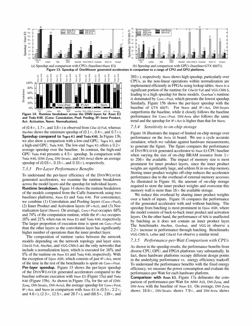
of (0.4×, 1.7×, and 3.8×) is observed from Cifar-10 Full, whereasAlexNet shows the minimum speedup of (0.1×, 0.4×, and 0.7×).Speedup compared to Tegra K1 and Tesla K40. In Figure 13b,we also show a comparison with a low-end GPU, Tegra K1, anda high-end GPU, Tesla K40. The low-end Tegra K1 offers a 0.2×average speedup over the baseline. In contrast, the high-endGPU Tesla K40 presents a 4.5× speedup. In comparison withTesla K40, (DW-Zynq, DW-Stratix, and DW-Arria) show an averagespeedup of (0.03×, 0.15×, and 0.33×), respectively.7.3.3 Per-Layer Performance BenefitsTo understand the per-layer efficiency of the DNNWEAVERgenerated accelerators, we examine the runtime breakdownacross the model layers and the speedup for individual layers.Runtime breakdown. Figure 14 shows the runtime breakdownof the models computed from the Caffe framework using twobaselines platforms, Xeon E3 and Tesla K40. For convenience,we combine (1) Convolution and Pooling layers (Conv+Pool),(2) Inner Product and Activation layers (IP+Act), and (3) Nor-malization layer (Norm). On average, Conv+Pool occupies 68%and 74% of the computation runtime, while the IP+Act occupies16% and 21% when run on Xeon E3 and Tesla K40, respectively.The larger proportion of execution time is spent on Conv+Pool
than the other layers as the convolution layer has significantlyhigher number of operations than the inner product layer.
The composition of runtime varies between the networkmodels depending on the network topology and layer sizes.Cifar10 Full, AlexNet, and VGG-CNN-S are the only networks thatinclude a normalization layer, which is executed for 16% and5% of the runtime on Xeon E3 and Tesla K40, respectively. Withthe exception of Djinn ASR, which consists of just IP+Act, mostof the time in the rest of the benchmarks is spent on Conv+Pool.Per-layer speedup. Figure 15 shows the per-layer speedupof the DNNWEAVER generated accelerators compared to thebaseline software execution with Xeon E3 (Figure 15a) and Tesla
K40 (Figure 15b). As shown in Figure 15a, for the set of (DW-
Zynq, DW-Stratix, DW-Arria), the average speedup for Conv+Pool,IP+Act, and Norm in comparison with Xeon E3 is (0.5×, 2.2×,and 4.6×), (2.3×, 12.5×, and 28.7×), and (68.5×, 139×, and
393×), respectively. Norm shows high speedup, particularly overCPUs, as the non-linear operations within normalization areimplemented efficiently in FPGAs using lookup tables. Norm is asignificant portion of the runtime for Cifar10 Full and VGG-CNN-S,leading to a high speedup for these models. Overfeat’s runtimeis dominated by Conv+Pool, which presents the lowest speedup.Similarly, Figure 15b shows the per-layer speedup with thebaseline of GTX 650Ti. For Norm and IP+Act, DW-Stratix
outperforms the baseline, while it closely follows the baselineperformance for Conv+Pool. DW-Arria also follows the sametrend and the speedup for IP+Act is higher than that for Norm.7.3.4 Sensitivity to on-chip storageFigure 16 illustrates the impact of limited on-chip storage overperformance on the Arria 10 board. We use a cycle accuratesimulator, which we validate against hardware measurements,to generate the figure. The figure compares the performanceof DNNWEAVER generated accelerator to Xeon E3 CPU baselinewhen varying the size of on-chip BRAM resource from 1×to 256× the available. The impact of memory size is mostprominent for inner product layers, since the inner productweights are significantly large, and seldom fit in on-chip memory.Storing inner product weights off-chip reduces the acceleratorperformance due to the overhead of external memory accesses.As illustrated in Figure 16, the amount of on-chip storagerequired to store the inner product weights and overcome thismemory wall is more than 16× the available storage.
We reduce this overhead by sharing inner product weightsover a batch of inputs. Figure 16 compares the performanceof the generated accelerator with and without batching. Thespeedup from batching is most prominent in Djinn ASR, wherethe model consists of back-to-back inner product and activationlayers. On the other hand, the performance of NiN is unaffectedby batching as it does not contain an inner product layer.The benchmarks AlexNet, Overfeat, and VGG-16 observe a2.2× increase in performance through batching. BenchmarksVGG-CNN-S, LeNet and Cifar10 Full observe a similar trend.7.3.5 Performance-per-Watt Comparison with CPUsAs shown in the speedup results, the performance benefits fromdiverse CPU, GPU, and FPGA platforms vary substantially. Infact, these hardware platforms occupy different design pointsin the underlying performance vs. energy efficiency tradeoff.To understand the performance benefits with the fixed energyefficiency, we measure the power consumption and evaluate theperformance-per-Watt for each hardware platform.Comparison with Xeon E3. Figure 17a delineates the com-parison of performance-per-Watt for ARM A15, DW-Zynq, andDW-Arria with the baseline of Xeon E3. On average, DW-Zynq
shows 16.6×, DW-Stratix shows 7.9×, and DW-Arria shows

1.6
158.
8
176.
5
1.4
87
0.3 0.
7
0.5
0.2
30.2
0.2 0.
3
60.3
0.2 0.
3
0.3 0.
6
0.5
2.3
68.5
7.7
747.
1
830.
3
6.7
409.
3
1.4 3.
6
2.3
1.4
40.2
1.2 2.
2
80.4
1 1.4
1.3 3 2.
2
12.5
139
17.4
1680
.9
15.1
921
2.5
8.2
4.3
3.2
137.
5
2.6 5.
1
236.
9
2.1 3.
2
2.9 7 4.
6
28.7
393.
3
0⨉
2⨉
40⨉
800⨉Co
nv+P
ool
IP+A
ct
Norm
Conv
+Poo
l
IP+A
ct
Conv
+Poo
l
IP+A
ct
Conv
+Poo
l
IP+A
ct
Norm
Conv
+Poo
l
IP+A
ct
Norm
Conv
+Poo
l
IP+A
ct
Conv
+Poo
l
IP+A
ct
Conv
+Poo
l
IP+A
ct
Norm
Cifar10 Full LeNet NiN Djinn ASR
AlexNet VGG-CNN-S Overfeat VGG-16 Geomean
Spee
dup
/ Xeo
n E3
(log
)DW-Zynq DW-Stratix DW-Arria
(a) Speedup for each DNN layer with the baseline of Xeon E3.
0.1
26.3
29
15.3
17
0.1
0.1
0.1
0.3
0.3
0.1
1.1
0.3
0.1
1.6
0.1
1.7
0.2
2.7
1.3
0.7
123.
8
136.
3
72.1
79.9
0.4 0.5
0.3
1.7
0.3 0.
6
8.3
0.4 0.
7
8
0.5
8.3
1
14.5
2.6
1.5
278.
6
306.
6
162.
2
179.
7
0.8 1
0.6
3.9
1.2
1.3
19.2
1.1 1.4
18.5
1.1
19.2
2.2
33.1
7.3
0⨉
2⨉
40⨉
800⨉
Conv
+Poo
l
IP+A
ct
Norm
Conv
+Poo
l
IP+A
ct
Conv
+Poo
l
IP+A
ct
Conv
+Poo
l
IP+A
ct
Norm
Conv
+Poo
l
IP+A
ct
Norm
Conv
+Poo
l
IP+A
ct
Conv
+Poo
l
IP+A
ct
Conv
+Poo
l
IP+A
ct
Norm
Cifar10 Full LeNet NiN Djinn ASR
AlexNet VGG-CNN-S Overfeat VGG-16 Geomean
Spee
dup
/ GTX
650
Ti (l
og )
DW-Zynq DW-Stratix DW-Arria
(b) Speedup for each DNN layer with the baseline of GTX 650Ti.Figure 15: Per-layer speedup when accelerated with DW-Zynq and DW-Arria.
NiN Djinn ASR
Memory0⇥
2⇥
4⇥
6⇥
8⇥
10⇥
Spe
edup
/Xeo
nE
3
1⇥ 4⇥ 16⇥ 64⇥ 256⇥
0.2
0.2
7.9
7.9
7.9
7.7
7.7
7.7
7.7
7.7
w/o batchingw/ batching
AlexNet
Memory0⇥
2⇥
4⇥
6⇥
8⇥
10⇥
Spe
edup
/Xeo
nE
31⇥ 4⇥ 16⇥ 64⇥ 256⇥
1.5
1.5
1.5
4.3
4.3
4.3
4.3
4.3
4.3
4.3
w/o batchingw/ batching
Overfeat
Memory0⇥
2⇥
4⇥
6⇥
8⇥
10⇥
Spe
edup
/Xeo
nE
3
1⇥ 4⇥ 16⇥ 64⇥ 256⇥
0.8
0.8
0.8
2.2
2.2
2.2
2.2
2.2
2.2
2.2
w/o batchingw/ batching
VGG-16
Memory0⇥
2⇥
4⇥
6⇥
8⇥
10⇥
Spe
edup
/Xeo
nE
3
1⇥ 4⇥ 16⇥ 64⇥ 256⇥
2.1
2.1
2.1 2.
9
2.9
2.9
2.9
2.9
2.9
2.9
w/o batchingw/ batching
Memory0⇥
2⇥
4⇥
6⇥
8⇥
10⇥
Spe
edup
/Xeo
nE
3
1⇥ 4⇥ 16⇥ 64⇥ 256⇥
2.5
2.5
2.5
2.5
2.5
2.5
2.5
2.5
2.5
2.5
w/o batchingw/ batching
Figure 16: Speedup over Xeon E3 when varying the available on-chip storage. We use a validated cycle-accurate simulator to generate these results.
0×
10×
20×
30×
40×
50×
Perfo
rman
cepe
rWat
t
Cifar10full LeNet NiN
DjinnASR AlexNet VGG-CNN-S Overfeat VGG-16 Gmean
3.3
2.3
1.4
1.7
1.1
0.9
1.0
1.0
1.4
74
38
11
21
10
13
7.5 8.3
16
34
17
4.5
11
5.0 6.4
3.6
4.2 7.
9
64
33
6.7
20
7.8 11
6.3 8.0
13ARM A15DW-Zynq
DW-StratixDW-Arria
(a) CPU Performance-per-Watt Comparison (Baseline=Xeon E3)
0×
1×
2×
3×
4×
5×
Perfo
rman
cepe
rWat
t
Cifar10full LeNet NiN
DjinnASR AlexNet VGG-CNN-S Overfeat VGG-16 Gmean
2.5
1.2
1.8
1.3
2.0 2.
3
0.5 0.
9
1.4
1.3
0.9
2.0
1.7 2.
1
3.2
4.5
2.4
2.0
6
3.2
2.7
2.0
1.9
3.8
5
2.5
3.2
3.1
1.5
1.1
1.1
0.9
1.8
2.7
1.3 1.
5
5
2.8
1.6 2.
0
1.4
3.4
4.7
2.5 2.
7
Tegra K1Tesla K40DW-Zynq
DW-StratixDW-Arria
(b) GPU Performance-per-Watt Comparison (Baseline=GTX 650Ti)Figure 17: Performance-per-Watt of the DnnWeaver generated accelerators in comparison to a range of CPU and GPU platforms.
13.9× higher performance-per-Watt than the baseline. Note thatalthough DW-Stratix provides about 10× higher speedup, theincreased power consumption by DW-Stratix (2W vs. 25W) leadsto the lower performance-per-Watt than DW-Zynq. However,DW-Arria provides higher performance that DW-Stratix, withouta commensurate increase in power consumption, leading tohigher performance-per-Watt. This trend is observed for all theevaluated DNN models.Comparison with ARM A15. Low-end processors such as ARM
A15 are commonly used in mobile devices and are known to havehigh energy-efficiency. We also compare the ARM A15 processorwith our accelerators and Xeon E3. The ARM A15 processor shows1.4× higher performance-per-Watt compared to Xeon E3. Whencompared with ARM A15, DW-Zynq, DW-Stratix, and DW-Arria
show 11.5×, 5.5×, and 9.6× higher performance-per-Watt,which demonstrates the energy efficiency of the DNNWEAVERgenerated accelerators.7.3.6 Performance-per-Watt Comparison with GPUsComparison with GTX 650Ti. Figure 17b shows theperformance-per-Watt in comparison of Tegra K1, Tesla K40,DW-Zynq, and DW-Arria with the baseline, GTX 650Ti. Thepair of (DW-Zynq, DW-Stratix, and DW-Arria) provides (3.2×,1.5×, and 2.7×) higher performance-per-Watt than the baseline.Although DW-Arria outperforms DW-Zynq with the speedupof 10× shown in Figure 13b, DW-Zynq offers a 1.2× higherperformance-per-Watt compared to DW-Arria.Comparison with Tegra K1 and Tesla K40. Figure 17b alsocompares the performance-per-Watt of Tegra K1 and Tesla K40
with the baseline. On average, Tegra K1 and Tesla K40 have 1.4×
and 2.0× higher performance-per-Watt than GTX 650Ti.7.3.7 Area and FPGA UtilizationTable 6 shows the framework determined number of PUsand the number of PEs-per-PU for DW-Zynq, DW-Stratix, andDW-Arria. The resource utilization in DW-Stratix is limited bythe LUTs available on chip, and the resource utilization inDW-Zynq is bounded by the number of BRAM blocks availableon-chip. Table 5 shows the resource utilization to generate theDNNWEAVER accelerators for each DNN model.
8 Related WorkThere have been several proposed and realized hardwaredesigns that accelerate machine learning algorithms andDNNs. However, this work differs from other efforts in thatDNNWEAVER is not an accelerator, but an accelerator generator.Our work produces an optimized design for a given (DNN,FPGA) pair. Furthermore, DNNWEAVER provides a novel ISAto unify DNN accelerators across different FPGA platforms.In this section we discuss the most related work in the area ofFPGA implementations and ASIC accelerators for DNNs.FPGA implementations for machine learning. Tabla [22]provides an FPGA accelerator generator for the training phase ofstatistical machine learning algorithms. However, DNNWEAVERfocuses on inference with DNNs. In addition, Tabla usesstochastic gradient descent as the abstraction between hardwareand software, and has no notion of ISA or Deep NeuralNetworks. Tabla provides its own mathematical language, whileDNNWEAVER uses Berkeley Caffe for model specification.
The work by Chen, et al. [14] focuses on using an analytical

Table 5: Resource utilization on the three FPGA platforms for each benchmark DNN.
Utilization Utilization Utilization Utilization Utilization Utilization Utilization Utilization Utilization UtilizationCifar-10 Full 61.44% 98.57% 30.77% 61.82% 85.29% 95.33% 46.90% 37.74% 84.99% 84.92% 45.85% 94.86%Djinn ASR 42.43% 100.00% 18.25% 63.64% 53.98% 85.80% 28.12% 36.23% 68.96% 94.36% 39.27% 98.81%
LeNet 47.57% 100.00% 21.90% 61.82% 66.53% 80.44% 32.83% 33.96% 84.99% 84.92% 45.85% 94.86%VGG_CNN_S 62.22% 97.14% 29.73% 61.82% 88.07% 78.50% 50.81% 37.04% 84.64% 89.64% 47.59% 88.54%
VGG_16 65.92% 100.00% 31.23% 63.64% 87.65% 78.20% 50.68% 37.42% 84.64% 89.64% 47.59% 88.54%AlexNet 64.56% 100.00% 30.78% 63.64% 86.70% 77.16% 50.04% 37.23% 82.19% 86.69% 46.24% 88.54%
NiN 68.59% 100.00% 34.62% 63.64% 86.70% 77.16% 50.04% 37.23% 84.64% 89.64% 47.59% 88.54%Overfeat 61.52% 94.29% 29.28% 60.00% 84.68% 75.07% 48.79% 36.98% 85.57% 86.25% 48.19% 88.93%
Flip-Flops (Total: 1708800)
DSP Slices (Total: 1518)
Utilization Utilization
Xilinx Zynq ZC702
LUTs(Total: 53200)
Flip-Flops (Total: 106400)
LUTs(Total:
Altera Arria 10 GX115
LUTs(Total:
BRAM (Bytes)(Total: 5035KB)
Flip-Flops (Total: 690000)
DSP Slices (Total: 1590)
BRAM (Bytes)(Total: 6782KB)Benchmark
DNN
Altera Stratix V SGSD5
BRAM (Bytes)(Total: 630KB)
DSP Slices (Total : 220)
Table 6: Total number of PUs and the number of PEs per PU built onthe three FPGA platforms for each benchmark DNN.
Benchmark # of PUs # of PEs # of PUs # of PEs # of PUs # of PEs Cifar10 full 8 17 8 60 8 135Djinn ASR 7 20 23 24 23 54MNIST LeNet 8 17 8 60 8 135VGG_CNN_S 17 8 17 31 19 64VGG_16 10 14 15 35 19 64AlexNet 14 10 14 37 14 84NiN 7 20 14 37 19 64Overfeat 12 11 12 42 13 90
Altera Arria 10 GX115Xilinx Zynq ZC702 Altera Stratix V SGSD5
design scheme based on the roofline model to find the fastestdesign for a particular DNN for FPGA acceleration. However,their design does not support some DNN layers such as poolingand normalization. The work by Farabet, et al. [15, 28] developsan FPGA accelerator for a specific DNN. Gokhale, et al. [27]propose a mobile co-processor for DNNs and evaluate iton a Zynq board. Chakradhar, et al. [38] present a VLIWco-processor for DNNs and emulate it on a Virtex 5 FPGA.They propose a special switch that allows to dynamically groupthe convolution engines in different ways. The design has alow-level VLIW ISA but the paper does not include any detailsabout its design. Unlike DNNWEAVER, they do not generateVerilog code for FPGA accelerators. The works by Qiu et al.and Suda et al. [39, 40] present implementations of acceleratorsfor particular DNN models. Neither of these works supportgeneration of accelerators for arbitrary DNN topologies.
DNNWEAVER makes FPGAs accessible to the machinelearning community by automatically generating an optimizedaccelerator from high level DNN specifications. On the otherhand, previous works come short of providing at least one ofthe following features: optimized accelerator generation, ISAsupport, a workflow starting from high level abstractions.ASIC accelerators for DNNs. Recent research efforts presentlow-power deep learning ASICs. For example, (Da)Diannao[12, 13] provide DNN accelerators with a low-level fine-grainedISA, yet they do not define an ISA to unify DNN accelerators.In contrast, DNNWEAVER uses a ISA for deep neural networks(DNN) representing high-level operations (layers) that providesthe flexibility necessary to optimize the accelerator microar-chitecture for the FPGA platform and DNN model. Sim, etal. [24] showcase a DNN ASIC for IoT devices. However, thearticle doesn’t make a reference to classification layer support.Qadeer, et al. [25] propose Convolution Engine which reducesthe number of operations required in convolution layers. Conti,et al. [26] develop convolution cores designed to integrate with ashared-memory cluster of RISC processors. PuDianNao [20] isan ASIC accelerator for machine learning algorithms but lacksdeep convolutional networks support.
All of these previous efforts require ASIC design, not FPGArealization, which is the focus of our work.Concurrent submissions. Hardware implementation forDNNs is a thriving and active area of research. The follow-ing efforts have been published concurrently to our work. Wang,
et al. [41] use a library of fixed-function blocks to accelerateDNNs on Xilinx Z7020 and Z7045 FPGAs. Unlike the PEs inDNNWEAVER, the architecture in their work lack explicit datasharing. Liu, et al. [42] propose an ISA for neural networks op-timized for high code density over vector and matrix operations.Chen, et al. [23, 43] develop an ASIC design with a 2D spatial ar-ray of PEs for Convolutional Neural Networks. Song, et al. [44]propose an ASIC implementation with adaptive data-level par-allelism for DNN accelerators. EIE [45], Minerva [46], and Cn-vlutin [47] propose ASIC accelerators that use operation pruningand quantization in DNNs for power and performance benefits.
9 ConclusionDeep Neural Networks are gaining increasing applicability andare amongst the most important workloads that can significantlybenefit from acceleration. However, DNNs are in a state of fluxand new disruptive advances require hardware solutions thatcan adapt to these changes. DNNWEAVER is an initial step inproviding such solutions that support a wide variety of DNNmodels and can be further extended for more advanced models.While GPUs serve as an attractive platform for DNNs, our resultsshows that FPGAs can be a Pareto optimal choice when poweris constraining. Nonetheless, reducing the programmer involve-ment in hardware design is imperative to the adoption of FPGAsin this domain. To this end, DNNWEAVER converts high-levelspecification of DNNs into highly efficient accelerators that op-erate within a limited power budget and on-chip memory of theFPGA. The conversion is made possible by a novel dataflow ISAand a heuristic search algorithm that generates high performanceaccelerator by customizing the hand-optimized template designsfor a given (DNN, FPGA) pair. DNNWEAVER takes an effectivestep in making FPGAs available to a broader community ofDNN developers who often do not possess hardware designexpertise. Community engagement and contribution are vital forproviding a general platform for DNN acceleration. To facilitatesuch engagement, DNNWEAVER has been made publiclyavailable at http://act-lab.org/artifacts/dnnweaver.
10 AcknowledgementsWe thank the anonymous reviewers for their insightful commentsand feedback. We thank Bradley Thwaites, Manan Chugh,Sushant Kumar Singh, and Payal Bagga. This work wassupported in part by NSF awards CCF #1553192 and CNS#1526211, Semiconductor Research Corporation contract #2015-TS-2636, and gifts from Google, Qualcomm, and Microsoft.
References[1] Yangqing Jia, Evan Shelhamer, Jeff Donahue, Sergey Karayev, Jonathan
Long, Ross Girshick, Sergio Guadarrama, and Trevor Darrell. Caffe:Convolutional architecture for fast feature embedding. arXiv preprintarXiv:1408.5093, 2014.
[2] Johann Hauswald, Michael A. Laurenzano, Yunqi Zhang, Cheng Li,Austin Rovinski, Arjun Khurana, Ron Dreslinski, Trevor Mudge, ViniciusPetrucci, Lingjia Tang, and Jason Mars. Sirius: An open end-to-end voice
and vision personal assistant and its implications for future warehousescale computers. In ASPLOS, 2015.
[3] Alex Graves, A-R Mohamed, and Geoffrey Hinton. Speech recognitionwith deep recurrent neural networks. In ICASSP, 2013.
[4] Yann LeCun, Bernhard Boser, John S Denker, Donnie Henderson,Richard E Howard, Wayne Hubbard, and Lawrence D Jackel. Backprop-agation applied to handwritten zip code recognition. Neural computation,1(4):541–551, 1989.
[5] Geoffrey Hinton, Simon Osindero, and Yee-Whye Teh. A fast learning al-gorithm for deep belief nets. Neural computation, 18(7):1527–1554, 2006.
[6] Alex Krizhevsky, Ilya Sutskever, and Geoffrey E Hinton. Imagenetclassification with deep convolutional neural networks. In NIPS, 2012.
[7] Johann Hauswald, Yiping Kang, Michael A Laurenzano, Quan Chen,Cheng Li, Trevor Mudge, Ronald G Dreslinski, Jason Mars, and LingjiaTang. Djinn and tonic: Dnn as a service and its implications for futurewarehouse scale computers. 2015.
[8] Ren Wu, Shengen Yan, Yi Shan, Qingqing Dang, and Gang Sun. Deep im-age: Scaling up image recognition. arXiv preprint arXiv:1501.02876, 2015.
[9] Adam Coates, Adam Coates, Brody Huval, Tao Wang, David J. Wu, andAndrew Y." Ng. Deep learning with cots hpc systems.
[10] Hadi Esmaeilzadeh, Emily Blem, Renee St. Amant, KarthikeyanSankaralingam, and Doug Burger. Dark silicon and the end of multicorescaling. In ISCA, 2011.
[11] N. Hardavellas, M. Ferdman, B. Falsafi, and A. Ailamaki. Toward darksilicon in servers. IEEE Micro, 31(4):6–15, July–Aug. 2011.
[12] Tianshi Chen, Zidong Du, Ninghui Sun, Jia Wang, Chengyong Wu, YunjiChen, and Olivier Temam. Diannao: A small-footprint high-throughputaccelerator for ubiquitous machine-learning. In ASPLOS, 2014.
[13] Yunji Chen, Tao Luo, Shaoli Liu, Shijin Zhang, Liqiang He, Jia Wang,Ling Li, Tianshi Chen, Zhiwei Xu, Ninghui Sun, et al. Dadiannao: Amachine-learning supercomputer. In MICRO, 2014.
[14] Chen Zhang, Peng Li, Guangyu Sun, Yijin Guan, Bingjun Xiao, and JasonCong. Optimizing fpga-based accelerator design for deep convolutionalneural networks. In FPGA, 2015.
[15] Clément Farabet, Berin Martini, Benoit Corda, Polina Akselrod, EugenioCulurciello, and Yann LeCun. Neuflow: A runtime reconfigurabledataflow processor for vision. In CVPRW, 2011.
[16] Ganesh Venkatesh, Jack Sampson, Nathan Goulding, Saturnino Gar-cia, Vladyslav Bryksin, Jose Lugo-Martinez, Steven Swanson, andMichael Bedford Taylor. Conservation cores: Reducing the energy ofmature computations. In ASPLOS, 2010.
[17] Venkatraman Govindaraju, Chen-Han Ho, and Karthikeyan Sankaralingam.Dynamically specialized datapaths for energy efficient computing. InHPCA, 2011.
[18] Shantanu Gupta, Shuguang Feng, Amin Ansari, Scott Mahlke, and DavidAugust. Bundled execution of recurring traces for energy-efficient generalpurpose processing. In MICRO, 2011.
[19] Andrew Putnam, Adrian Caulfield, Eric Chung, Derek Chiou, KyprosConstantinides, John Demme, Hadi Esmaeilzadeh, Jeremy Fowers, GopiPrashanth, Jan Gray, Michael Haselman, Scott Hauck, Stephen Heil, AmirHormati, Joo-Young Kim, Sitaram Lanka, James R. Larus, Eric Peterson,Aaron Smith, Jason Thong, Phillip Yi Xiao, and Doug Burger. A reconfig-urable fabric for accelerating large-scale datacenter services. In ISCA, 2014.
[20] Daofu Liu, Tianshi Chen, Shaoli Liu, Jinhong Zhou, Shengyuan Zhou,Olivier Teman, Xiaobing Feng, Xuehai Zhou, and Yunji Chen. Pudiannao:A polyvalent machine learning accelerator. In ASPLOS, 2015.
[21] Zidong Du, Robert Fasthuber, Tianshi Chen, Paolo Ienne, Ling Li, TaoLuo, Xiaobing Feng, Yunji Chen, and Olivier Temam. Shidiannao: shiftingvision processing closer to the sensor. In ISCA, 2015.
[22] Divya Mahajan, Jongse Park, Emmanuel Amaro, Hardik Sharma, AmirYazdanbakhsh, Joon Kyung Kim, and Hadi Esmaeilzadeh. Tabla: Aunified template-based framework for accelerating statistical machinelearning. In HPCA, pages 14–26. IEEE, 2016.
[23] Yu-Hsin Chen, Tushar Krishna, Joel S. Emer, and Vivienne Sze. 14.5 eye-riss: An energy-efficient reconfigurable accelerator for deep convolutionalneural networks. In ISSCC, 2016.
[24] J. Sim, J. S. Park, M. Kim, D. Bae, Y. Choi, and L. S. Kim. 14.6 a1.42tops/w deep convolutional neural network recognition processor forintelligent ioe systems. In ISSCC, 2016.
[25] Wajahat Qadeer, Rehan Hameed, Ofer Shacham, Preethi Venkatesan,
Christos Kozyrakis, and Mark A Horowitz. Convolution engine: balancingefficiency & flexibility in specialized computing. In ACM SIGARCHComputer Architecture News, volume 41, pages 24–35. ACM, 2013.
[26] Francesco Conti and Luca Benini. A ultra-low-energy convolution enginefor fast brain-inspired vision in multicore clusters. In DATE, 2015.
[27] Vinayak Gokhale, Jonghoon Jin, Aysegul Dundar, Berin Martini, andEugenio Culurciello. A 240 g-ops/s mobile coprocessor for deep neuralnetworks. In CVPRW, 2014.
[28] Clément Farabet, Berin Martini, Polina Akselrod, Selçuk Talay, YannLeCun, and Eugenio Culurciello. Hardware accelerated convolutionalneural networks for synthetic vision systems. In ISCAS, 2010.
[29] Yann LeCun, Léon Bottou, Yoshua Bengio, and Patrick Haffner. Gradient-based learning applied to document recognition. Proceedings of the IEEE,86(11):2278–2324, 1998.
[30] Alex Krizhevsky. One weird trick for parallelizing convolutional neuralnetworks. arXiv preprint arXiv:1404.5997, 2014.
[31] Pierre Sermanet, David Eigen, Xiang Zhang, Michaël Mathieu, RobFergus, and Yann LeCun. Overfeat: Integrated recognition, localizationand detection using convolutional networks. CoRR, abs/1312.6229, 2013.
[32] Alex Krizhevsky and Geoffrey Hinton. Learning multiple layers of featuresfrom tiny images. Computer Science Department, University of Toronto,Tech. Rep, 1(4):7, 2009.
[33] Yann LeCun and Corinna Cortes. MNIST handwritten digit database, 2010.[34] Min Lin, Qiang Chen, and Shuicheng Yan. Network in network. CoRR,
abs/1312.4400, 2013.[35] K. Chatfield, K. Simonyan, A. Vedaldi, and A. Zisserman. Return of
the devil in the details: Delving deep into convolutional nets. In BritishMachine Vision Conference, 2014.
[36] Olga Russakovsky, Jia Deng, Hao Su, Jonathan Krause, Sanjeev Satheesh,Sean Ma, Zhiheng Huang, Andrej Karpathy, Aditya Khosla, MichaelBernstein, Alexander C. Berg, and Li Fei-Fei. ImageNet Large ScaleVisual Recognition Challenge. IJCV, 115(3):211–252, 2015.
[37] Shaoyi Cheng and John Wawrzynek. High level synthesis with a dataflowarchitectural template. CoRR, abs/1606.06451, 2016.
[38] Srimat Chakradhar, Murugan Sankaradas, Venkata Jakkula, and SrihariCadambi. A dynamically configurable coprocessor for convolutionalneural networks. In ACM SIGARCH Computer Architecture News,volume 38, pages 247–257. ACM, 2010.
[39] Naveen Suda, Vikas Chandra, Ganesh Dasika, Abinash Mohanty, YufeiMa, Sarma Vrudhula, Jae-sun Seo, and Yu Cao. Throughput-optimizedopencl-based fpga accelerator for large-scale convolutional neural networks.In FPGA, 2016.
[40] Jiantao Qiu, Jie Wang, Song Yao, Kaiyuan Guo, Boxun Li, Erjin Zhou,Jincheng Yu, Tianqi Tang, Ningyi Xu, Sen Song, et al. Going deeper withembedded fpga platform for convolutional neural network. In FPGA, 2016.
[41] Ying Wang, Jie Xu, Yinhe Han, Huawei Li, and Xiaowei Li. Deepburning:Automatic generation of fpga-based learning accelerators for the neuralnetwork family. In Proceedings of the 53rd Annual Design Automation Con-ference, DAC ’16, pages 110:1–110:6, New York, NY, USA, 2016. ACM.
[42] Shaoli Liu, Zidong Du, Jinhua Tao, Dong Han, Tao Luo, Yuan Xie, YunjiChen, and Tianshi Chen. Cambricon: An instruction set architecture forneural networks. In ISCA, 2016.
[43] Yu-Hsin Chen, Joel Emer, and Vivienne Sze. Eyeriss: A spatial architecturefor energy-efficient dataflow for convolutional neural networks. 2016.
[44] Lili Song, Ying Wang, Yinhe Han, Xin Zhao, Bosheng Liu, and XiaoweiLi. C-brain: A deep learning accelerator that tames the diversity of cnnsthrough adaptive data-level parallelization. In Proceedings of the 53rdAnnual Design Automation Conference, DAC ’16, pages 123:1–123:6,New York, NY, USA, 2016. ACM.
[45] Song Han, Xingyu Liu, Huizi Mao, Jing Pu, Ardavan Pedram, Mark A.Horowitz, and William J. Dally. EIE: efficient inference engine oncompressed deep neural network. CoRR, abs/1602.01528, 2016.
[46] Brandon Reagen, Paul Whatmough, Robert Adolf, Saketh Rama,Hyunkwang Lee, Sae Kyu Lee, Jose Miguel Hernandez-Lobato, Gu-YeonWei, and David Brooks. Minerva: Enabling low-power, highly-accuratedeep neural network accelerators. In ISCA, 2016.
[47] Jorge Albericio, Patrick Judd, Tayler Hetherington, Tor Aamodt, Natalie En-right Jerger, and Andreas Moshovos. Cnvlutin: Ineffectual-neuron-freedeep neural network computing. In ISCA, 2016.


![A Common Framework for Interactive Texture Transfer...The neural doodle reported in [8] using convo-lutional neural networks fails to reproduce clear and high-quality images with low-level](https://img.dokumen.tips/doc/110x75/611dc841c689be2b342b9e84/a-common-framework-for-interactive-texture-transfer-the-neural-doodle-reported.jpg)