Embed Size (px)
Citation preview

© September 25, 2014 Dr. Lynn Fuller, Professor
Rochester Institute of Technology
Microelectronic Engineering
Frequency Response
Page 1
ROCHESTER INSTITUTE OF TECHNOLOGY MICROELECTRONIC ENGINEERING
9-25-14 Frequency_Response.ppt
Frequency Response of the CE Amplifier
Dr. Lynn Fuller Webpage: http://people.rit.edu/lffeee/
Microelectronic Engineering Rochester Institute of Technology
82 Lomb Memorial Drive Rochester, NY 14623-5604
Tel (585) 475-2035
Email: [email protected] MicroE webpage: http://www.microe.rit.edu
© September 25, 2014 Dr. Lynn Fuller, Professor
Rochester Institute of Technology
Microelectronic Engineering
Frequency Response
Page 2
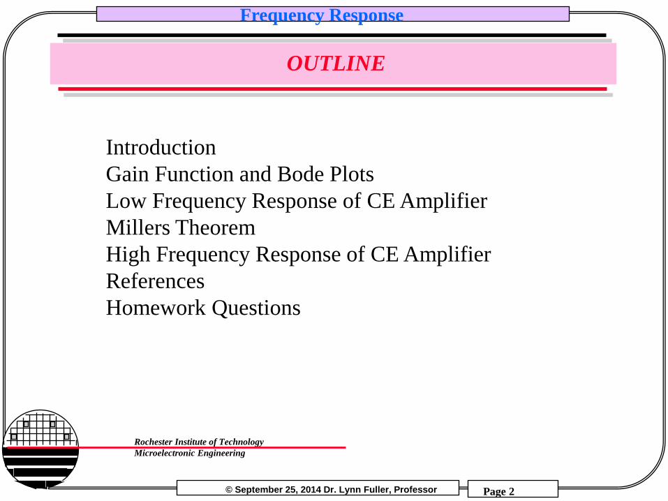
OUTLINE
Introduction
Gain Function and Bode Plots
Low Frequency Response of CE Amplifier
Millers Theorem
High Frequency Response of CE Amplifier
References
Homework Questions

© September 25, 2014 Dr. Lynn Fuller, Professor
Rochester Institute of Technology
Microelectronic Engineering
Frequency Response
Page 3
INTRODUCTION
We will be interested in the voltage gain of an electronic circuit as a function of frequency.
Vout Vin Av = Vout/Vin
Decibel: the gain of some network can be expressed in logarithmic units. When this is done the overall gain of cascaded networks can be found by simple addition of the individual network gains. The decibel is defined as: Ap = 10 log (Po/Pin) dB where Ap is the power gain in decibels Po is the power out and Pin is the power in The decibel has also been used as a unit for voltage gain. Po = Vout2/RL and Pin = Vin2/Rin and if Rin=RL Ap = 20 log (Vout/Vin) dB
© September 25, 2014 Dr. Lynn Fuller, Professor
Rochester Institute of Technology
Microelectronic Engineering
Frequency Response
Page 4
INTRODUCTION
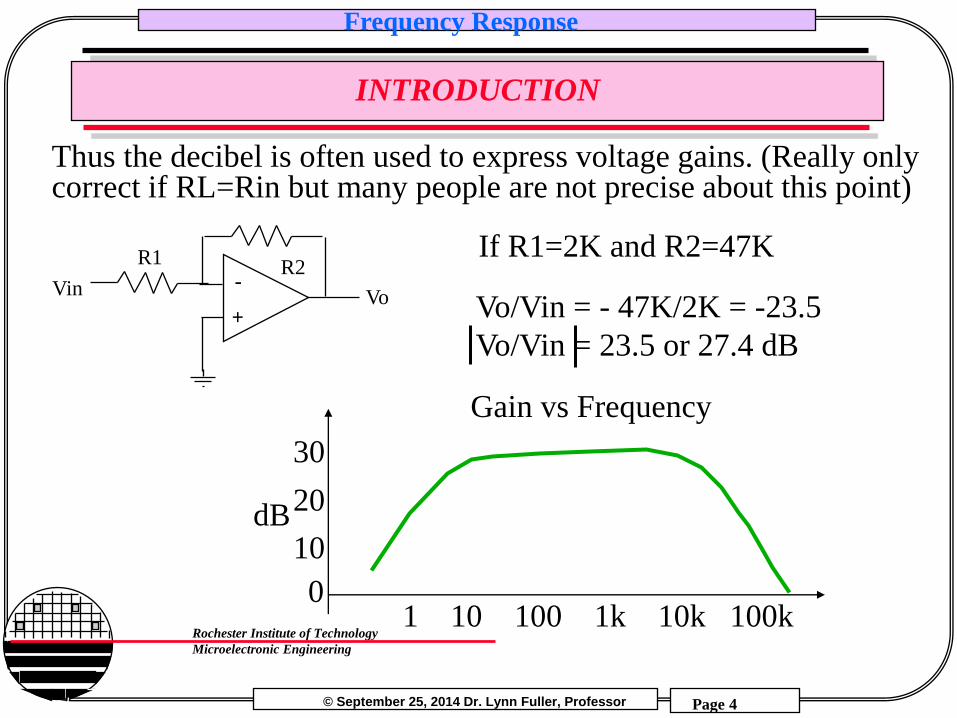
Thus the decibel is often used to express voltage gains. (Really only correct if RL=Rin but many people are not precise about this point)
-
+ Vo Vin
R2 R1 If R1=2K and R2=47K
Vo/Vin = - 47K/2K = -23.5
Vo/Vin = 23.5 or 27.4 dB
1 10 100 1k 10k 100k
Gain vs Frequency
0
10
20
30
dB

© September 25, 2014 Dr. Lynn Fuller, Professor
Rochester Institute of Technology
Microelectronic Engineering
Frequency Response
Page 5
THE GAIN FUNCTION
The gain function, A(s): an expression for Vo/Vin which is found in a straight forward manor from the ac equivalent circuit.
Vo/Vin = A(s) or in particular s=jw thus A(jw)
a0 + a1 s + a2 s2 + a3 s3 …. b0 + b1 s + b2 s2 + b3 s3 ….
A(s) =
K (s-z1)(s-z2)(s-z3)… (s-p1)(s-p2)(s-p3)…
A(s) =
Where z1, z2, z3 are zeros, p1, p2, p3 are poles
K (jw-z1)(jw-z2)(jw-z3)… (jw-p1)(jw-p2)(jw-p3)…
A(jw) =
A0 (jw/w1)N(jw/w3+1)(jw/w5+1)… (jw/w2+1)(jw/w4+1)(jw/w6+1)…
A(jw) =

© September 25, 2014 Dr. Lynn Fuller, Professor
Rochester Institute of Technology
Microelectronic Engineering
Frequency Response
Page 6
GOALS
1. Obtain the gain function from the ac equivalent circuit.
2. Predict the frequency response of the gain function.
3. Use graphical techniques to sketch the frequency response
3. Introduce a new model for transistors at high frequencies.
5. Analyze and predict the frequency response of a common
emitter amplifier stage
© September 25, 2014 Dr. Lynn Fuller, Professor
Rochester Institute of Technology
Microelectronic Engineering
Frequency Response
Page 7
GRAPHICAL TECHNIQUES AND BODE PLOTS
Vo = Vin 1/sC
R + 1/sC
Vo/Vin = 1/jwC
R + 1/jwC 1
jwRC + 1 =
1
jw/w1+ 1 =
Where w1 = 1/RC and f1 = 1 / 2 p RC
Vin + -
R
C Vout
Bode Plot: a plot of the gain function versus frequency (w or f). Note: both magnitude and phase are a function of frequency. The Bode Plot plots this information separately.
Gain Function:
w
w
Vo/V
s (d
B)
Log10 scale
Log10 scale Phas
e (D
egre
es)

© September 25, 2014 Dr. Lynn Fuller, Professor
Rochester Institute of Technology
Microelectronic Engineering
Frequency Response
Page 8
CONTINUE PREVIOUS EXAMPLE 1
Av = Vo/Vin = jw/w1 + 1
1
At low w Vo/Vin = 1 0° Vo/Vin dB = 0 dB and ; Q = 0°
At high w Vo/Vin = 1/(jw/w1) -90°
Vo/Vin dB = w1/w dB and Q = -90°
Note: at w = 10 w1 Vo/Vin dB = -20 dB
Note: at w = 100 w1 Vo/Vin dB = -40 dB
Thus we see at high frequencies the gain decreases by -20 dB / decade

© September 25, 2014 Dr. Lynn Fuller, Professor
Rochester Institute of Technology
Microelectronic Engineering
Frequency Response
Page 9
CONTINUE EXAMPLE 1
w
w
Vo/V
s (d
B)
Log10 scale
Phas
e (D
egre
es)
w1
-45
-90
0dB -3dB
-20dB

© September 25, 2014 Dr. Lynn Fuller, Professor
Rochester Institute of Technology
Microelectronic Engineering
Frequency Response
Page 10
EXAMPLE 2
Vin + -
R C Vout
Obtain the gain function for the network shown. Sketch the magnitude part of the Bode Plot.
© September 25, 2014 Dr. Lynn Fuller, Professor
Rochester Institute of Technology
Microelectronic Engineering
Frequency Response
Page 11
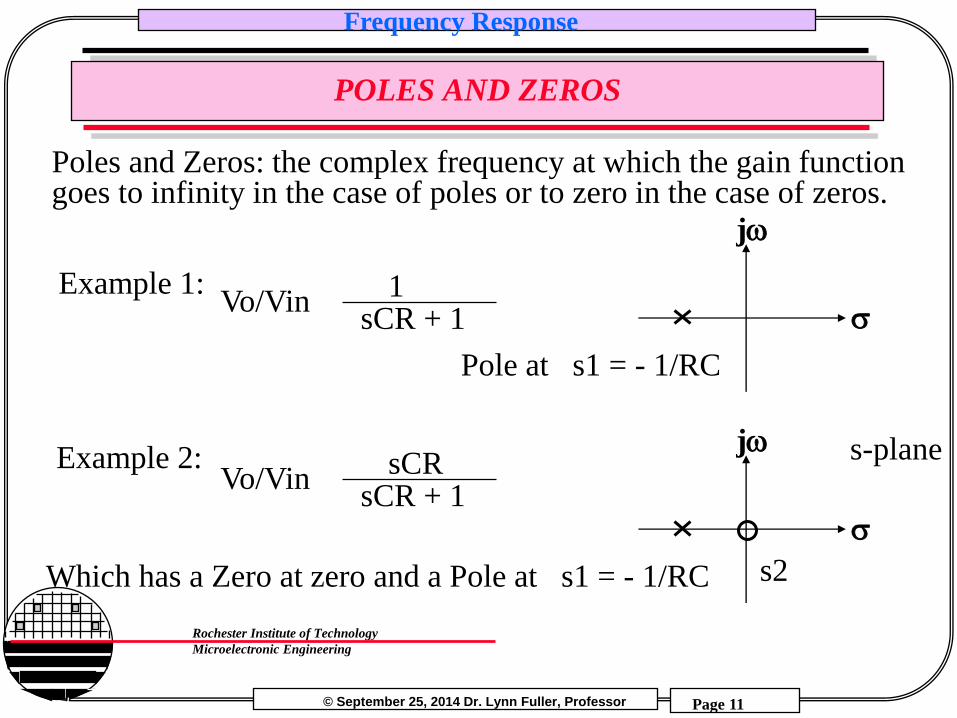
POLES AND ZEROS
Poles and Zeros: the complex frequency at which the gain function goes to infinity in the case of poles or to zero in the case of zeros.
Vo/Vin 1
sCR + 1 Example 1:
Example 2:
jw
s
Pole at s1 = - 1/RC
Vo/Vin sCR
sCR + 1
jw
s
Which has a Zero at zero and a Pole at s1 = - 1/RC
s-plane
s2

© September 25, 2014 Dr. Lynn Fuller, Professor
Rochester Institute of Technology
Microelectronic Engineering
Frequency Response
Page 12
CORNER FREQUENCY
Vo/Vin = 1
jwCR + 1 Example 1:
Example 2:
Has a corner at w1 = 1/RC or f = 1/2pRC
Vo/Vin = jwCR
jwCR + 1
Has a corner w1 = 1/RC
Corner frequencies: that frequency (f or w) at which the real and imaginary parts of one term of the gain function are equal/
© September 25, 2014 Dr. Lynn Fuller, Professor
Rochester Institute of Technology
Microelectronic Engineering
Frequency Response
Page 13
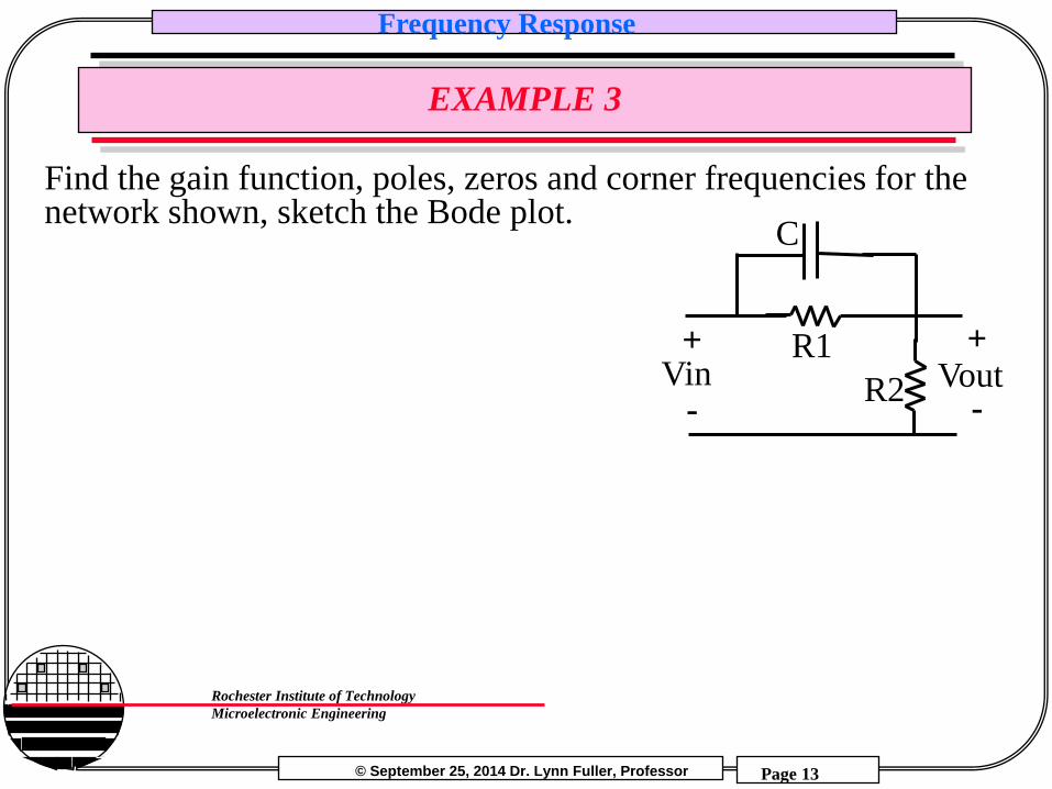
EXAMPLE 3
Find the gain function, poles, zeros and corner frequencies for the network shown, sketch the Bode plot.
Vin R1
C
Vout R2
+
-
+
-

© September 25, 2014 Dr. Lynn Fuller, Professor
Rochester Institute of Technology
Microelectronic Engineering
Frequency Response
Page 14
LOW FREQUENCY MODEL OF CE AMPLIFIER
Effect of the Coupling Capacitor, Cc assume Ce, and Cc2 act like a short. Obtain the gain function from the ac equivalent circuit:
Vcc
Rc
vs +
-
R1
vo
Re R2
RL
Rs +
-
Cc
Ce
Cc2
Rs
RL
ro gmvbe
or
bib rp vbe
+
-
vo
+
-
vs +
- Rc
Rth Cc
vo = -gm vbe Ry
Ry = ro//Rc//RL
vbe =
Rx = Rth//rp
(Rs+1/sCc + Rx) vs Rx
vo/vs = -gm Rx Ry
(Rs+1/sCc + Rx)
s = jw
© September 25, 2014 Dr. Lynn Fuller, Professor
Rochester Institute of Technology
Microelectronic Engineering
Frequency Response
Page 15
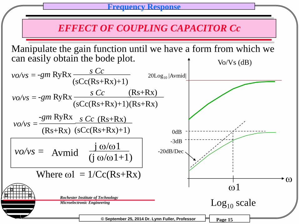
EFFECT OF COUPLING CAPACITOR Cc
Manipulate the gain function until we have a form from which we can easily obtain the bode plot.
vo/vs = s Cc
(sCc(Rs+Rx)+1) -gm RyRx
vo/vs = s Cc
(sCc(Rs+Rx)+1) -gm RyRx
(Rs+Rx)
(Rs+Rx)
vo/vs = s Cc
(sCc(Rs+Rx)+1)
-gm RyRx
(Rs+Rx)
(Rs+Rx)
vo/vs = j w/w1
(j w/w1+1) Avmid
Where w1 = 1/Cc(Rs+Rx) w
Vo/Vs (dB)
Log10 scale
w1
0dB
-3dB
-20dB/Dec
20Log10 |Avmid|
© September 25, 2014 Dr. Lynn Fuller, Professor
Rochester Institute of Technology
Microelectronic Engineering
Frequency Response
Page 16
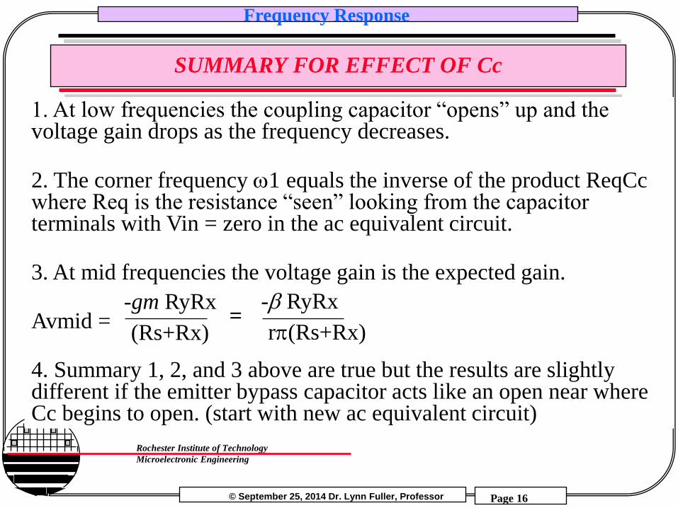
SUMMARY FOR EFFECT OF Cc
1. At low frequencies the coupling capacitor “opens” up and the voltage gain drops as the frequency decreases. 2. The corner frequency w1 equals the inverse of the product ReqCc where Req is the resistance “seen” looking from the capacitor terminals with Vin = zero in the ac equivalent circuit. 3. At mid frequencies the voltage gain is the expected gain. Avmid = 4. Summary 1, 2, and 3 above are true but the results are slightly different if the emitter bypass capacitor acts like an open near where Cc begins to open. (start with new ac equivalent circuit)
-gm RyRx
(Rs+Rx)
-b RyRx
rp(Rs+Rx) =

© September 25, 2014 Dr. Lynn Fuller, Professor
Rochester Institute of Technology
Microelectronic Engineering
Frequency Response
Page 17
EFFECT OF Ce ON FREQUENCY RESPONSE
The ac equivalent circuit of the CE amplifier on page 14 above is shown. Here we assume Cc is a short (note: it is possible that Cc acts like an open rather than a short)
Rs
RL
ro gmvbe
or
bib rp vbe
+
-
vo
+
-
vs +
- Rc
Rth
Let Rs = 0 and RL = ro = infinity to simplify the algebra
Ce Re

© September 25, 2014 Dr. Lynn Fuller, Professor
Rochester Institute of Technology
Microelectronic Engineering
Frequency Response
Page 18
EFFECT OF Ce ON FREQUENCY RESPONSE
vo = - b ib Rc vs = ib rp + (b+1) ib Re//(1/sCe)
vo/vs = -b Rc 1
rp + (b+1) Re//(1/sCe)
The gain function:
Manipulate the gain function:
vo/vs = -b Rc 1
rp + (b+1) Re/sCe Re + 1/sCe
= -b Rc 1
rp + (b+1) Re sCeRe + 1

© September 25, 2014 Dr. Lynn Fuller, Professor
Rochester Institute of Technology
Microelectronic Engineering
Frequency Response
Page 19
EFECT OF Ce ON FREQUENCY RESPONSE
vo/vs = = -b Rc rp + (b+1) Re (sCeRe + 1)
sCeRe + 1
= -b Rc + (b+1) Re sCeRe rp + rp
sCeRe + 1
rp + (b+1) Re -b Rc sCeRe + 1
sCeRe rp rp + (b+1) Re
+ 1
=
rp + (b+1) Re -b Rc (jw/we + 1)
(jw/we1 + 1)
Where: we = 1/Ce Re
we1 = 1/(Ce Re//(rp/(b+1)))
vo/vs =
k=Avlow Note: we1 is always > we
Note: Avmid = Avlow we1/we

© September 25, 2014 Dr. Lynn Fuller, Professor
Rochester Institute of Technology
Microelectronic Engineering
Frequency Response
Page 20
EFFECT OF Ce ON FREQUENCY RESPONSE
w
Vo/Vs (dB)
Log10 scale
we=/CeRe we1=1/CeReq
Avmid
Avlow
© September 25, 2014 Dr. Lynn Fuller, Professor
Rochester Institute of Technology
Microelectronic Engineering
Frequency Response
Page 21
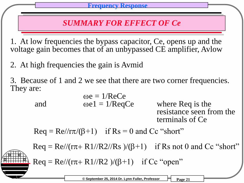
SUMMARY FOR EFFECT OF Ce
1. At low frequencies the bypass capacitor, Ce, opens up and the voltage gain becomes that of an unbypassed CE amplifier, Avlow 2. At high frequencies the gain is Avmid 3. Because of 1 and 2 we see that there are two corner frequencies. They are: we = 1/ReCe and we1 = 1/ReqCe where Req is the resistance seen from the terminals of Ce
Req = Re//rp/(b+1) if Rs = 0 and Cc “short”
Req = Re//(rp+ R1//R2//Rs )/(b+1) if Rs not 0 and Cc “short”
Req = Re//(rp+ R1//R2 )/(b+1) if Cc “open”

© September 25, 2014 Dr. Lynn Fuller, Professor
Rochester Institute of Technology
Microelectronic Engineering
Frequency Response
Page 22
COMPLETE CE AMPLIFIER LOW FREQUENCY RESPONSE
Vcc
Rc
vs +
-
R1
vo
Re R2
RL
Rs +
-
Cc
Ce
Cc2
Rs = 2K R1 = 40K R2 = 10K RC = 4K Re = 1K RL = 2K
vo/vs = K (jw/w1) (jw/w2) (jw/w3+1)
(jw/w1+1) (jw/w2+1) (jw/w4+1)
Find k, w1, w2, w3, w4
b = 100 Vcc = 20 Cc = Ce = Cc2 = 10µf
© September 25, 2014 Dr. Lynn Fuller, Professor
Rochester Institute of Technology
Microelectronic Engineering
Frequency Response
Page 23
EXAMPLE: SOLUTION
DC analysis:
Avmid = Voltage gain including RS and RL assume all C’s shorts
© September 25, 2014 Dr. Lynn Fuller, Professor
Rochester Institute of Technology
Microelectronic Engineering
Frequency Response
Page 24
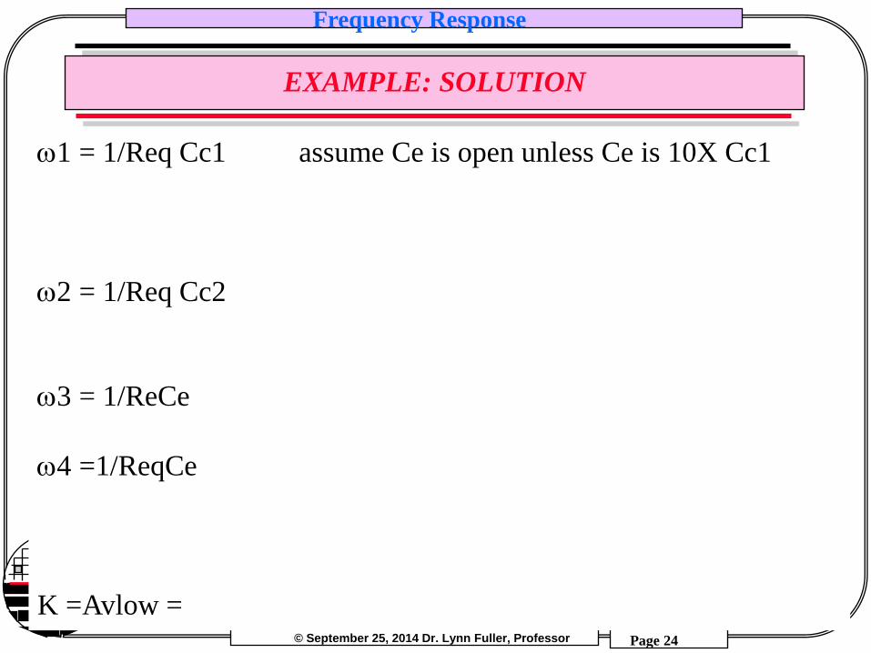
EXAMPLE: SOLUTION
w1 = 1/Req Cc1 assume Ce is open unless Ce is 10X Cc1
w2 = 1/Req Cc2
w3 = 1/ReCe
w4 =1/ReqCe
K =Avlow =

© September 25, 2014 Dr. Lynn Fuller, Professor
Rochester Institute of Technology
Microelectronic Engineering
Frequency Response
Page 25
HIGH FREQUENCY BJT TRANSISTOR MODEL
Rbb’ is the series base resistance rp is the base emitter small signal junction resistance Cb’e is the base emitter junction capacitance Cb’c is the base collector junction capacitance CD is the diffusion capacitance, represents the change in charge stored in the base caused by a change in base emitter voltage ro is the small signal output resistance = VA/IC b is the short circuit common emitter current gain
b ib rp
Rbb’
Cb’e
CD
Cb’c c b b’
e
ro ib

© September 25, 2014 Dr. Lynn Fuller, Professor
Rochester Institute of Technology
Microelectronic Engineering
Frequency Response
Page 26
MILLERS THEOREM
To predict the high frequency response of a common emitter amplifier we want to do some quick calculations. We would like to simplify the model given on the previous page. We can do this with the aid of Miller’s theorem. The resulting model is approximate and might not give good results above the upper corner frequency where the voltage gain begins to fall off.
Millers Theorem: Consider a linear network with N nodes. An impedance, Z, between any two nodes, N1 and N2, can be removed and another impedance Z1 placed from N1 to reference and impedance Z2 placed from N2 to reference. If Z1 = Z/(1-K) and Z2 = ZK/(K-1) where K=V2/V1, then the nodal equations will not be changed and the resulting circuit will yield equivalent node voltages, V1, V2, etc.

© September 25, 2014 Dr. Lynn Fuller, Professor
Rochester Institute of Technology
Microelectronic Engineering
Frequency Response
Page 27
MILLERS THEOREM
N1 N2 N2 N1
Z
Z1 Z2 Ref Ref
Z1 = Z/(1-K) Z2 = Z (K/(K-1))
where K=V2/V1
V1 V2 V1 V2
at N1 term (V1-V2)/Z at N1 term V1/Z1 = V1/(Z/(1-K))
= V1/(Z/(1-V2/V1))
= (V1-V2)/Z

© September 25, 2014 Dr. Lynn Fuller, Professor
Rochester Institute of Technology
Microelectronic Engineering
Frequency Response
Page 28
HIGH FREQUENCY MODEL OF CE AMPLIFIER
b ib rp
Rbb’
Cb’e
CD Cm’
c b b’
e
ro ib
Cm
From: Z1 = Z/(1-K) we have 1/sCm = 1/sCb’c 1-V2/V1
V2 = -b ib ro and V1 = ib rp
Therefore: Cm = Cb’c (1- - b ro/rp)
and : Cm’ = ~ Cb’c
From: Z2 = Z (K/(K-1)) Voltage gain

© September 25, 2014 Dr. Lynn Fuller, Professor
Rochester Institute of Technology
Microelectronic Engineering
Frequency Response
Page 29
EXAMPLE: HIGH FREQUENCY CE AMPLIFIER
Vcc
Rc
vs +
-
Rb
Iin
b ib rp vs +
- RB
Rbb’
CT iin
ib
RS
b = 100 rp = 1K, Rb’b = 0 Cb’c = 20pf Cb’e + CD = 20pf + 1000pf
RL
RL
Let CT = Cb’e + CD + Cm
and Cm = Cb’c(1- - b RL/rp)
To find the gain function: vo = - b ib Rc//RL ib = Vb’e/rp Vb’e = vs (RB//rp//(1/sCT)
RS + (RB//rp//(1/sCT)
Next pg
Rc

© September 25, 2014 Dr. Lynn Fuller, Professor
Rochester Institute of Technology
Microelectronic Engineering
Frequency Response
Page 30
EXAMPLE: HIGH FREQUENCY CE AMPLIFIER
vo/vs = - b Rc//RL
RS + (RB//rp//(1/sCT) rp
(RB//rp//(1/sCT) The gain function:
Manipulate the gain function: Let RB//rp = R
vo/vs = - b Rc//RL
rp
R(1/sCT)
R+ (1/sCT) R(1/sCT)
R+ (1/sCT) RS +
vo/vs = - b RL
rp
R
sCT R+ 1
R
s CT R+ 1 RS +
vo/vs = - b RL
rp R
(s CT R+ 1) RS + R
vo/vs = - b Rc//RL
rp R
s CT R RS (RS + R) 1
(RS + R) +1

© September 25, 2014 Dr. Lynn Fuller, Professor
Rochester Institute of Technology
Microelectronic Engineering
Frequency Response
Page 31
EXAMPLE: HIGH FREQUENCY CE AMPLIFIER
vo/vs = - b Rc//RL
rp R
jw CT R RS (RS + R) 1
(RS + R) +1
wh = 1/ CT (R//RS) Avmid
w
Vo/Vs (dB)
Log10 scale wh
20Log10 (Avmid)

© September 25, 2014 Dr. Lynn Fuller, Professor
Rochester Institute of Technology
Microelectronic Engineering
Frequency Response
Page 32
SUMMARY: HIGH FREQUENCY RESPONSE OF CE AMP
1. At high frequencies the internal capacitances in the transistor causes the voltage gain to decrease 2. At mid frequencies the gain is Avmid = 3. The corner frequency is wh = 1/ (Req CT) where CT = Cb’e + CD + Cm and Req = the equivalent resistance as “seen” from the terminals of the capacitor CT. (vs = zero) 4. There is a second corner due to the miller capacitance Cm’. Since wh occurs first we are not normally interested in the corner due to Cm’
- b Rc//RL
rp R
(RS + R)
© September 25, 2014 Dr. Lynn Fuller, Professor
Rochester Institute of Technology
Microelectronic Engineering
Frequency Response
Page 33
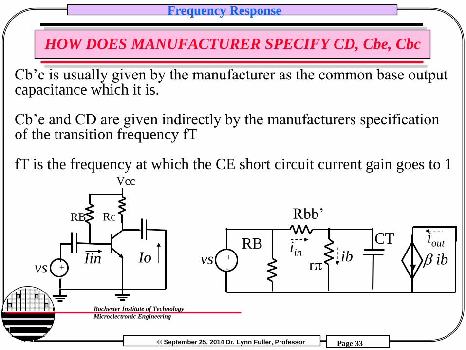
HOW DOES MANUFACTURER SPECIFY CD, Cbe, Cbc
Cb’c is usually given by the manufacturer as the common base output capacitance which it is. Cb’e and CD are given indirectly by the manufacturers specification of the transition frequency fT fT is the frequency at which the CE short circuit current gain goes to 1
Vcc
Rc
vs +
-
RB
Iin Io b ib rp vs +
-
RB
Rbb’
CT iin
iout ib

© September 25, 2014 Dr. Lynn Fuller, Professor
Rochester Institute of Technology
Microelectronic Engineering
Frequency Response
Page 34
2N3904
Rb = 10 ohms
© September 25, 2014 Dr. Lynn Fuller, Professor
Rochester Institute of Technology
Microelectronic Engineering
Frequency Response
Page 35
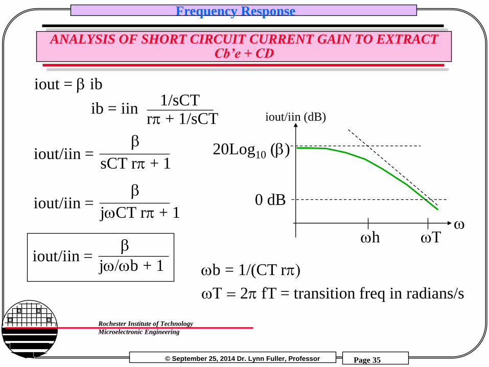
ANALYSIS OF SHORT CIRCUIT CURRENT GAIN TO EXTRACT Cb’e + CD
iout = b ib
ib = iin 1/sCT
rp + 1/sCT
iout/iin = b
sCT rp + 1
iout/iin = b
jwCT rp + 1
wb = 1/(CT rp)
w
iout/iin (dB)
wh
20Log10 (b)
0 dB
wT
wT = 2p fT = transition freq in radians/s
iout/iin = b
jw/wb + 1

© September 25, 2014 Dr. Lynn Fuller, Professor
Rochester Institute of Technology
Microelectronic Engineering
Frequency Response
Page 36
ANALYSIS OF SHORT CIRCUIT CURRENT GAIN TO EXTRACT Cb’e + CD
at wT, iout/in = 1 = ~ b
jw/wb
2 p fT = b
CT rp
So CT = b
2 p fT rp = Cb’e + CD + Cm
and Cm = Cb’c since Av = zero
Cb’e + CD = b
2 p fT rp - Cb’c
Finally
© September 25, 2014 Dr. Lynn Fuller, Professor
Rochester Institute of Technology
Microelectronic Engineering
Frequency Response
Page 37
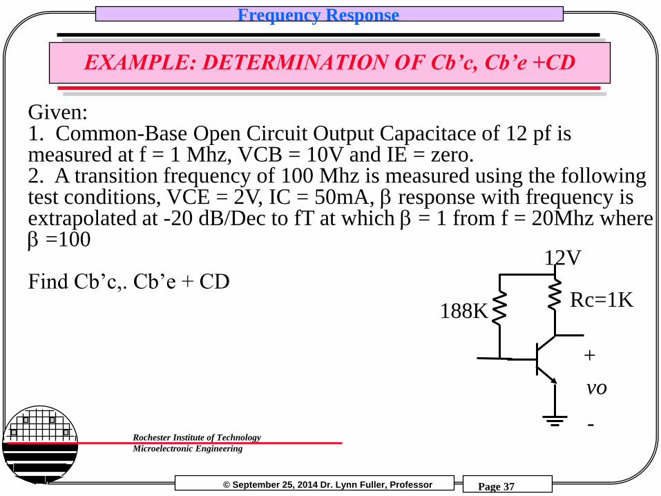
EXAMPLE: DETERMINATION OF Cb’c, Cb’e +CD
Given: 1. Common-Base Open Circuit Output Capacitace of 12 pf is measured at f = 1 Mhz, VCB = 10V and IE = zero. 2. A transition frequency of 100 Mhz is measured using the following test conditions, VCE = 2V, IC = 50mA, b response with frequency is extrapolated at -20 dB/Dec to fT at which b = 1 from f = 20Mhz where b =100 Find Cb’c,. Cb’e + CD
12V
Rc=1K 188K
vo
+
-

© September 25, 2014 Dr. Lynn Fuller, Professor
Rochester Institute of Technology
Microelectronic Engineering
Frequency Response
Page 38
SOLUTION TO EXAMPLE ON PREVIOUS PAGE

© September 25, 2014 Dr. Lynn Fuller, Professor
Rochester Institute of Technology
Microelectronic Engineering
Frequency Response
Page 39
ANOTHER EXAMPLE
Vcc
Rc
vs +
-
R1
vo
Rs +
-
Cc
Vcc = 15 Rs = 100 R1 = 150K RC = 500
Find rp, Cm, CT and wh
b = 100 VA = infinity Rb’b = 100 Cb’c = 20pf at Vcb = 5 fT = 100 Mhz
© September 25, 2014 Dr. Lynn Fuller, Professor
Rochester Institute of Technology
Microelectronic Engineering
Frequency Response
Page 40
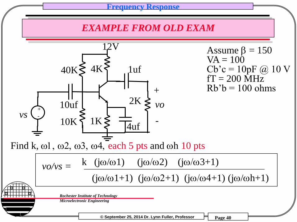
EXAMPLE FROM OLD EXAM
Find k, w1, w2, w3, w4, each 5 pts and wh 10 pts
Assume b = 150 VA = 100 Cb’c = 10pF @ 10 V fT = 200 MHz Rb’b = 100 ohms
vo/vs = k (jw/w1) (jw/w2) (jw/w3+1)
(jw/w1+1) (jw/w2+1) (jw/w4+1) (jw/wh+1)
12V
4K
vs +
-
40K
vo
1K 10K
2K +
-
10uf
4uf
1uf
© September 25, 2014 Dr. Lynn Fuller, Professor
Rochester Institute of Technology
Microelectronic Engineering
Frequency Response
Page 41
REFERENCES
1. Sedra and Smith, chapter 5.
2. Device Electronics for Integrated Circuits, 2nd Edition, Kamins
and Muller, John Wiley and Sons, 1986.
3. The Bipolar Junction Transistor, 2nd Edition, Gerald Neudeck,
Addison-Wesley, 1989.
4. Data sheets for 2N3904
© September 25, 2014 Dr. Lynn Fuller, Professor
Rochester Institute of Technology
Microelectronic Engineering
Frequency Response
Page 42
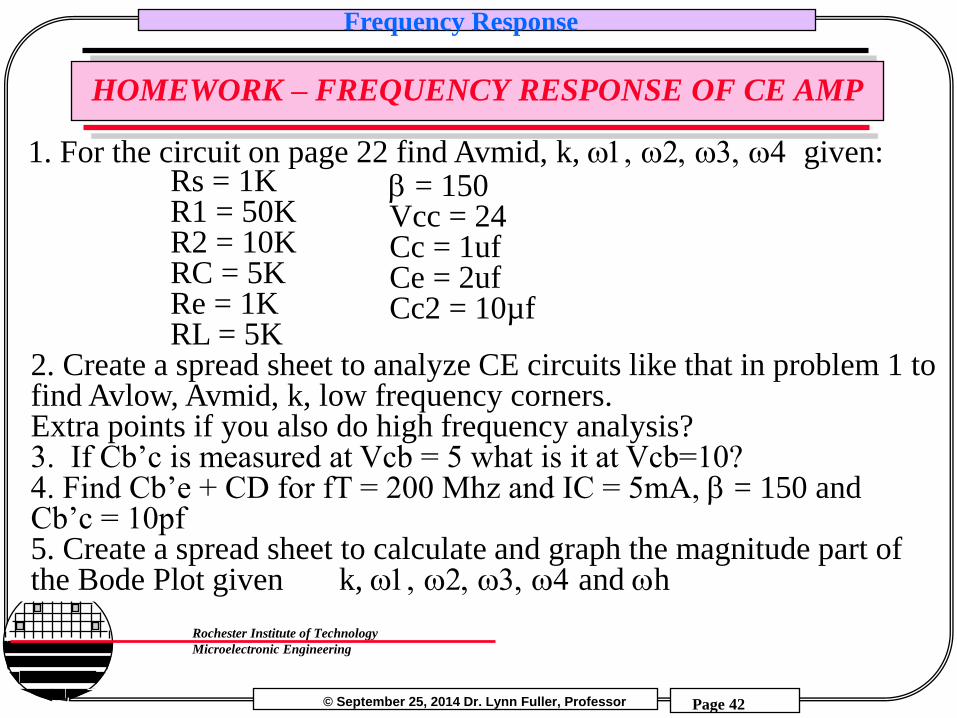
HOMEWORK – FREQUENCY RESPONSE OF CE AMP
1. For the circuit on page 22 find Avmid, k, w1, w2, w3, w4 given: Rs = 1K R1 = 50K R2 = 10K RC = 5K Re = 1K RL = 5K
b = 150 Vcc = 24 Cc = 1uf Ce = 2uf Cc2 = 10µf
2. Create a spread sheet to analyze CE circuits like that in problem 1 to find Avlow, Avmid, k, low frequency corners. Extra points if you also do high frequency analysis? 3. If Cb’c is measured at Vcb = 5 what is it at Vcb=10? 4. Find Cb’e + CD for fT = 200 Mhz and IC = 5mA, b = 150 and Cb’c = 10pf 5. Create a spread sheet to calculate and graph the magnitude part of the Bode Plot given k, w1, w2, w3, w4 and wh
© September 25, 2014 Dr. Lynn Fuller, Professor
Rochester Institute of Technology
Microelectronic Engineering
Frequency Response
Page 43
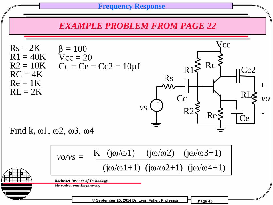
EXAMPLE PROBLEM FROM PAGE 22
Vcc
Rc
vs +
-
R1
vo
Re R2
RL
Rs +
-
Cc
Ce
Cc2
Rs = 2K R1 = 40K R2 = 10K RC = 4K Re = 1K RL = 2K
vo/vs = K (jw/w1) (jw/w2) (jw/w3+1)
(jw/w1+1) (jw/w2+1) (jw/w4+1)
Find k, w1, w2, w3, w4
b = 100 Vcc = 20 Cc = Ce = Cc2 = 10µf

© September 25, 2014 Dr. Lynn Fuller, Professor
Rochester Institute of Technology
Microelectronic Engineering
Frequency Response
Page 44
EXAMPLE pg 22: SOLUTION
DC analysis: Rth = R1//R2 = (10)(40)/(10+40) = 8K
Vth= Vcc R2/(R1+R2) = 20 (10)/(10+40) = 4V
KVL: IB Rth +0.7 +(B+1)IB Re – Vth = 0
IB = 4 - 0.7 / (Rth +101K) = 30.3uA
IC = B IB = 100 (30.3uA) = 3.03 mA
gm = IC/VT = 3.03/0.026 = 117 mS
rp = Vt/IB = 0.026/30.3uA = 858 ohms
ro = VA/IC = assume large
Avmid = Voltage gain including RS and RL assume all C’s shorts
Vo = gm Rc//RL Vin
Vin = Vs Rin/(Rin + Rs)
Vo/Vs = Vo/Vin x Vin/Vs = -(gmRC//RL ){Rin/(Rin+Rs)}
Vo/Vs = -117m (4K//2K) (Rth//rp)/((Rth//rp)+2K)
= - 43.6

© September 25, 2014 Dr. Lynn Fuller, Professor
Rochester Institute of Technology
Microelectronic Engineering
Frequency Response
Page 45
EXAMPLE pg 22: SOLUTION(continued)
w1 = 1/Req Cc1 assume Ce is open unless it is 10X Cc1
Req = Rs+Rth// (rp +(B+1)Re) = 2K+ 8K // (0.858K +101K)
= 9.42K
w1 = 1/ (9.42K 10 uF) = 10.6 r/s or 1.69 Hz
w2 = 1/Req Cc2
Req = RL + Rc = 6K
w2 = 1 / (6K 10uF) = 16.7 r/s or 2.65 Hz
w3 = 1/ReCe = 1/(1K 10uF) = 100 r/s or 15.9 Hz
w4 =1/ReqCe
Req = Re//((rp+Rth//Rs)/(B+1)) = 1K//((0.858K+8K//2K)/101)
= 24.3 ohms
w4 = 1/(24.3 10uF) = 4214 r/s or 671 Hz
K =Avlow = Avmid w3/w4 = -42 (100/4214) = -0.99

© September 25, 2014 Dr. Lynn Fuller, Professor
Rochester Institute of Technology
Microelectronic Engineering
Frequency Response
Page 46
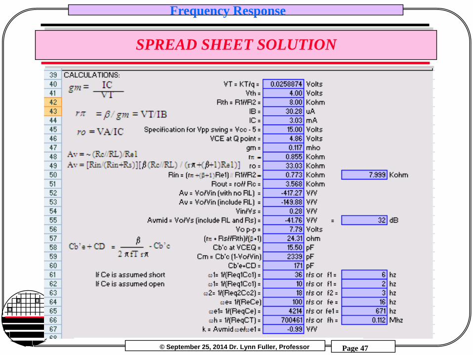
SPREAD SHEET SOLUTION
© September 25, 2014 Dr. Lynn Fuller, Professor
Rochester Institute of Technology
Microelectronic Engineering
Frequency Response
Page 47
SPREAD SHEET SOLUTION

© September 25, 2014 Dr. Lynn Fuller, Professor
Rochester Institute of Technology
Microelectronic Engineering
Frequency Response
Page 48
LTSPICE SOLUTION
32dB
700Hz

© September 25, 2014 Dr. Lynn Fuller, Professor
Rochester Institute of Technology
Microelectronic Engineering
Frequency Response
Page 49
SOLUTION
Given: 1. Common-Base Open Circuit Output Capacitace of 12 pf is measured at f = 1 Mhz, VCB = 10V and IE = zero. 2. A transition frequency of 100 Mhz is measured using the following test conditions, VCE = 2V, IC = 50mA, b response with frequency is extrapolated at -20 dB/Dec to fT at which b = 1 from f = 20Mhz where b =100 Find Cb’c,. Cb’e + CD First do DC analysis to find IC and VCB KVL IB 188K + 0.7 = 12 = 0 IB = (12-0.7)/188K = 60uA IC = Beta IB = 100 60uA = 6mA VCB = 12-Rc 6mA – 0.7 = 5.3 volts
12V
Rc=1K 188K
vo
+
-

© September 25, 2014 Dr. Lynn Fuller, Professor
Rochester Institute of Technology
Microelectronic Engineering
Frequency Response
Page 50
SOLUTION TO EXAMPLE ON PREVIOUS PAGE
Cb’e + CD = b
2 p fT rp - Cb’c
Find rp = 0.026/IB = 0.026/0.060 mA = 433 ohms Find Cb’c at the VCB of 5.3 volts = 12pF = 16.5 pF 10 volts
5.3 volts
Beta = 100 and fT = 100 MEG
Cb’e + CD = 368 pF – 16.5 pF = 352 pF

© September 25, 2014 Dr. Lynn Fuller, Professor
Rochester Institute of Technology
Microelectronic Engineering
Frequency Response
Page 51
SOLUTION
Vcc
Rc
vs +
-
R1
vo
Rs +
-
Cc
Vcc = 15 Rs = 100 R1 = 150K RC = 500
Find rp, Cm, CT and wh
b = 100 VA = infinity Rb’b = 100 Cb’c = 20pf at Vcb = 5 fT = 100 Mhz
First do DC analysis to find IC and VCB KVL IB 150K + 0.7 = 15 = 0 IB = (15-0.7)/150K = 95.3uA IC = Beta IB = 100 95.3uA = 9.53mA VCB = 15-Rc 9.53mA – 0.7 = 9.54 volts
© September 25, 2014 Dr. Lynn Fuller, Professor
Rochester Institute of Technology
Microelectronic Engineering
Frequency Response
Page 52
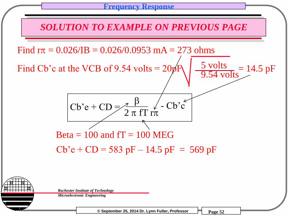
SOLUTION TO EXAMPLE ON PREVIOUS PAGE
Cb’e + CD = b
2 p fT rp - Cb’c
Find rp = 0.026/IB = 0.026/0.0953 mA = 273 ohms Find Cb’c at the VCB of 9.54 volts = 20pF = 14.5 pF 5 volts
9.54 volts
Beta = 100 and fT = 100 MEG
Cb’e + CD = 583 pF – 14.5 pF = 569 pF

© September 25, 2014 Dr. Lynn Fuller, Professor
Rochester Institute of Technology
Microelectronic Engineering
Frequency Response
Page 53
SOLUTION TO EXAMPLE ON PREVIOUS PAGE
Voltage gain Vo / Vb’e at mid frequencies is used for miller capacitance Calculations. Vo = -B ib RC//RL//ro = -100 ib 500 ib = Vb’e / rp = Vb’e / 273
Vo / Vb’e = -183
Cm = Cb’c (1- - 183) = 14.5 pF x 184 = 2668 pF CT = Cb’e + CD + Cm = 569 pF + 2668 pF = 3237 pF wh = 1 / Req CT Req = ((RS // Rth ) + Rbb’ ) // rp = 199.9 // 273 = 115 wh = 1 / Req CT = 1 / (115 x 3237 pF) = 2.69M r/s = 0.428 MHz

© September 25, 2014 Dr. Lynn Fuller, Professor
Rochester Institute of Technology
Microelectronic Engineering
Frequency Response
Page 54
COMPARE TO SPREAD SHEET