Embed Size (px)
Citation preview
PHYSICAL REVIEW B 95, 035203 (2017)
Frequency-dependent dielectric function of semiconductors with application to physisorption
Fan Zheng,1 Jianmin Tao,2,* and Andrew M. Rappe1
1The Makineni Theoretical Laboratories, Department of Chemistry, University of Pennsylvania, Philadelphia, Pennsylvania 19104-6323, USA2Department of Physics, Temple University, Philadelphia, Pennsylvania 19122-1801, USA
(Received 11 July 2016; published 11 January 2017)
The dielectric function is one of the most important quantities that describes the electrical and optical propertiesof solids. Accurate modeling of the frequency-dependent dielectric function has great significance in the studyof the long-range van der Waals (vdW) interaction for solids and adsorption. In this work we calculate thefrequency-dependent dielectric functions of semiconductors and insulators using the GW method with andwithout exciton effects, as well as efficient semilocal density functional theory (DFT), and compare thesecalculations with a model frequency-dependent dielectric function. We find that for semiconductors with moderateband gaps, the model dielectric functions, GW values, and DFT calculations all agree well with each other.However, for insulators with strong exciton effects, the model dielectric functions have a better agreement withaccurate GW values than the DFT calculations, particularly in high-frequency region. To understand this, werepeat the DFT calculations with scissors correction, by shifting the DFT Kohn-Sham energy levels to match theexperimental band gap. We find that scissors correction only moderately improves the DFT dielectric functionin the low-frequency region. Based on the dielectric functions calculated with different methods, we make acomparative study by applying these dielectric functions to calculate the vdW coefficients (C3 and C5) foradsorption of rare-gas atoms on a variety of surfaces. We find that the vdW coefficients obtained with the nearlyfree electron gas-based model dielectric function agree quite well with those obtained from the GW dielectricfunction, in particular for adsorption on semiconductors, leading to an overall error of less than 7% for C3 and5% for C5. This demonstrates the reliability of the model dielectric function for the study of physisorption.
DOI: 10.1103/PhysRevB.95.035203
I. INTRODUCTION
The frequency-dependent dielectric response function, asthe linear-order response to electric field, plays a centralrole in the study of the electrical and optical propertiesof solids. It is related to many properties of materials. Inparticular, the static dielectric function has been used in theconstruction of density functional approximations [1,2] forthe exchange-correlation energy. The frequency-dependentdielectric function provides important screening for the vander Waals (vdW) interaction in solids, because it has beenused as an ingredient in the calculation of vdW interactionsfor physisorption and layered materials [3], which has beenone of the most interesting topics in condensed matter physics.However, calculation of this quantity presents a great challengeto semilocal density functional theory (DFT) [4–6], the mostpopular electronic structure method. A fundamental reason isthat, while DFT can describe the ground-state properties well,it tends to underestimate excitation energies and the band gap,due to the absence of electronic nonlocality. For example,the widely used local spin-density approximation (LSDA)and the generalized-gradient approximation (GGA) lack theelectron-hole interaction information for excitons and thediscontinuity of energy derivative with respect to the number ofelectrons [7–10]. The GW approximation [11] for the electronself-energy provides a highly accurate method for describingthe single-particle spectra of electrons and holes. It yieldsaccurate fundamental band gaps of solids [12,13]. Based on theGW approximation, the Bethe-Salpeter equation (BSE) can besolved to capture electron-hole interactions [14,15]. Therefore,
*[email protected]; http://www.sas.upenn.edu/∼jianmint/
GW+BSE has been widely used to calculate optical spectraand light absorption, and the results are used as references forother methods [16–18]. However, as a cost of high accuracy,this method is computationally demanding, and thus it is notpractical for large systems. As such, accurate modeling of thedielectric functions of semiconductors and insulators with asimple analytic function of frequency is highly desired.
Many model dielectric functions have been proposed [19–23]. Most of them have been devoted to the static limit, whilethe study of the frequency-dependent dielectric function isquite limited. Based on a picture of the nearly free electron gas,Penn derived a simple model dielectric function. This modelwas modified by Breckenridge, Shaw, and Sher to satisfy theKramers-Kronig relation [24]. The modified Penn model hasbeen used to calculate the vdW coefficient C3 for the adsorp-tion of atoms on surfaces [25] and the dielectric screeningeffect for the vdW interaction in solids [26]. In particular, Taoand Rappe [27] have recently applied the frequency-dependentmodel dielectric function and a simple yet accurate modeldynamic multipole polarizability to calculate the leading-orderas well as higher-order vdW coefficients C3 and C5 for atomson a variety of solid surfaces. The results are consistentlyaccurate.
To have a better understanding of this model dielectricfunction, in the present work we perform GW quasiparticlecalculations and solve the BSE, aiming to provide a robustreference for benchmarking the model frequency-dependentdielectric function. To achieve this goal, we compare themodel dielectric functions with the high-level GW calculationsfor several typical semiconductors and insulators: silicon,diamond, GaAs, LiF, NaF, and MgO. As an interestingcomparison, we also calculate the dielectric function withthe GGA exchange-correlation functional [4]. Based on these
2469-9950/2017/95(3)/035203(8) 035203-1 ©2017 American Physical Society

FAN ZHENG, JIANMIN TAO, AND ANDREW M. RAPPE PHYSICAL REVIEW B 95, 035203 (2017)
dielelctric calculations, the vdW coefficients on the varioussurfaces are also calculated and compared to reference values.To have a better understanding of the performance of DFT, werepeat our DFT dielectric function calculation after shifting theKohn-Sham eigenenergies to match experimental band gaps(scissors correction) [28].
II. COMPUTATIONAL DETAILS
A. Model dielectric function
The Penn model is perhaps the most widely used modeldielectric function for semiconductors. It was derived fromthe nearly free electron gas. However, this model violates theKramers-Kronig relation [19]. To fix this problem, Brecken-ridge, Shaw, and Sher [24] proposed a modification, in whichthe imaginary part takes the expression
ε2(ω) = πω2p
[ωg − �
(ω2 − ω2
g
)1/2]2/[2ω3
(ω2 − ω2
g
)1/2].
(1)
Here ω is a real frequency within the range ωg � ω �4εF
√1 + �2 [25,27], ωp = √
4πn, εF = (3π2n)2/3/2 is theFermi energy, and n is the average valence electron densityof the bulk solid. � = ωg/4εF , and ωg is the effective energygap, which can be determined from optical dielectric constantε1(0) by solving the Penn’s model:
ε1(0) = 1 + (ω2
p/ω2g
)(1 − �). (2)
Here we use this expression to calculate ωg from theexperimental static dielectric constant for diamond, LiF, NaF,and MgO. [In Ref. [27] the ab initio values of ε1(0), ratherthan experimental values, were used. Since the two sets ofvalues are very close to each other, it does not make anoticeable difference.] For other materials, ε1(0) values aretaken from the literature [24,29]. The real part of the dielectricfunction can be obtained from the Kramers-Kronig relationε1(ω) = 1 + 1
πP
∫ +∞−∞ dω′ε2(ω′)/(ω′ − ω). The result is given
by [26]
ε1(iu) = 1 + ω2p
u2
⎡⎣ (1 − �2)y
P− ω2
g − (ω2
g + u2)�2
2u√
ω2g + u2
lnI+I−
⎤⎦
+ 2ω2p�
u2
{ωg
u
[tan−1
(ωgP
u
)− tan−1
(ωg
u
)]
+ 1
P− 1
}, (3)
where I± = [(1 + y2)(1 + u2/ω2g)]1/2 ± uy/ωg , y = 1/�,
and P = (1 + y2)1/2. Vidali and Cole [25] found that thismodel dielectric function agrees well with experimental valuesof GaAs [30–33].
B. DFT calculations
The DFT calculation of the dielectric function for solidswas performed with the plane-wave density functional theory(DFT) package QUANTUM ESPRESSO [34], with the GGAexchange-correlation functional [4]. The norm-conserving,designed nonlocal pseudopotentials were generated with the
OPIUM package [35,36]. With the single-particle approxima-tion, the imaginary part of the dielectric response function inthe long-wavelength limit can be expressed as
ε2,j (ω) = π
2ε0
e2
m2(2π )4�ω2
∑c,v
∫BZ
dk|〈c,k|pj |v,k〉|2
× δ(ωc,k − ωv,k − ω). (4)
In this equation, c and v represent the conduction andvalence bands with eigenenergy �ωn, and k is the Blochwave vector. In Cartesian coordinates, j indicates x, y, orz. In practice, the real part of the dielectric function ε1(iu),expressed in terms of the imaginary frequency iu, can beobtained from the imaginary part via the Kramers-Kronigrelation. Here, in order to avoid the pole structure whenintegrating over the real frequency, the imaginary frequency isused.
It is well known that semilocal DFT tends to underestimatethe band gaps of semiconductors and insulators. To understandthe role of band gap, we repeated the DFT calculation,replacing the Kohn-Sham HOMO-LUMO energy gap with theexperimental [28] or calculated band gap from high-level (e.g.,GW or GW+BSE) methods [37]. This scissors correctionwill allow us to study the band gap effect on the dielectricfunction [38] by
ωmn = ωGGAmn + �ω, (5)
where ωmn is the energy difference between bands m and n, and�ω is the scissor correction for reproducing the experimentalband gap. In this work, this correction is applied to theinsulators via the rigid shifting of the imaginary part of thedielectric functions.
C. GW and BSE calculations
The GW calculations including electron-electron screeningare carried out using the BerkeleyGW package [39–41]. In theGW approximation, the quasiparticle energy is given by
EQPnk = EMF
nk + 〈ψn,k|�(E) − VXC|ψn,k〉, (6)
where � is the self-energy and ψnk is a mean-field wavefunction. VXC is the exchange-correlation potential obtainedfrom the GGA or LDA functional. The mean-field part ofthe DFT electronic structure calculations was performed withQUANTUM ESPRESSO. First, the static dielectric matrix ε(q; 0)within the random-phase approximation (RPA) is calculated.Then, the generalized plasmon pole and static Coulomb holeand screened exchange approximation (COHSEX) were usedto evaluate the self-energy �. In order to have accuratequasiparticle energies, the convergence of band energies witha number of empty bands in the dielectric matrix and Coulombhole (COH) self-energy evaluations and the convergenceversus plane-wave cutoff were carefully tested [42]. WhileGW can yield the self-energy precisely for charged excitationsand reveal the fundamental band gap, neutral excitation (suchas optical absorption) requires consideration of the electron-hole interaction. Due to the significance of this interaction indetermining the optical response, the BSE was solved to revealthe effect of excitons on light absorption. This is particularlyimportant for ionic solids, such as LiF, NaF, and MgO, with
035203-2
FREQUENCY-DEPENDENT DIELECTRIC FUNCTION OF . . . PHYSICAL REVIEW B 95, 035203 (2017)
strongly bound excitons. To perform BSE calculations, theelectron-hole kernel terms evaluated on a coarse k point gridwere interpolated onto a dense grid. By diagonalizing thekernel matrix, exciton eigenvalues S and eigenfunctions |S〉were solved and used in the calculation of the optical dielectricfunction [40]:
ε2(ω) = 16π2e2
ω2
∑S
|e · 〈0|v|S〉|2δ(ω − ωS), (7)
where S is the exciton state with exciton energy ωS , e is thedirection of the light polarization, and v is the velocity operator.The dielectric function with imaginary frequency dependencecan be easily obtained.
D. vdW coefficients
The vdW interaction is crucial for adsorption of atomsor molecules on solid surfaces, while adsorption on solidsis fundamentally important in probing the surface structuresand properties of bulk solids (e.g., atomic or molecular beamscattering) as well as catalysis and hydrogen storage (e.g.,surface adsorption on fullerenes, nanotubes, and graphene). Inthe process of physisorption, the instantaneous multipole dueto the electronic charge fluctuations of a solid will interact withthe dipole, quadrupole, and octupole moments of adsorbedatoms or molecules, giving rise to vdW attraction. However,semilocal DFT often fails to describe this process, becausethe long-range vdW interaction is missing in semilocal DFT.Many attempts [26,43–56] have been made to capture thislong-range part, such as nonlocal vdW-DF functional [43]and density functional dispersion correction [57,58]. It hasbeen shown that with a proper dispersion correction, theperformance of ordinary DFT methods can be significantlyimproved [27]. This combined DFT+vdW method has beenwidely used in electronic structure calculations of moleculesand solids [54,59–62].
The vdW coefficients for adsorption on solid surfaces werecalculated in terms of the dielectric function and the dynamicmultipole polarizability. The dynamic multipole polarizabilitywas computed from a simple yet accurate model describedin Refs. [53,54]. The electronic charge density was obtainedfrom Hartree-Fock calculations using GAMESS [63,64]. Withthe imaginary frequency-dependent dielectric function and theatomic polarizabilities, the vdW coefficients C3 and C5 werecalculated from [27,65,66]
C2l+1 = 1
4π
∫ ∞
0duαl(iu)
ε1(iu) − 1
ε1(iu) + 1, (8)
where l = 1 describes the interaction of the instantaneousdipole moment of an atom with the surface, while l = 2describes the interaction of the quadrupole moment of theatom with the surface. ε1 is the real part of the dielectricfunction of the bulk solid, and αl(iu) is the dynamic multipolepolarizability.
III. RESULTS AND DISCUSSION
A. Dielectric function
The experimental values of the frequency-dependent di-electric function are not directly available in the literature, but
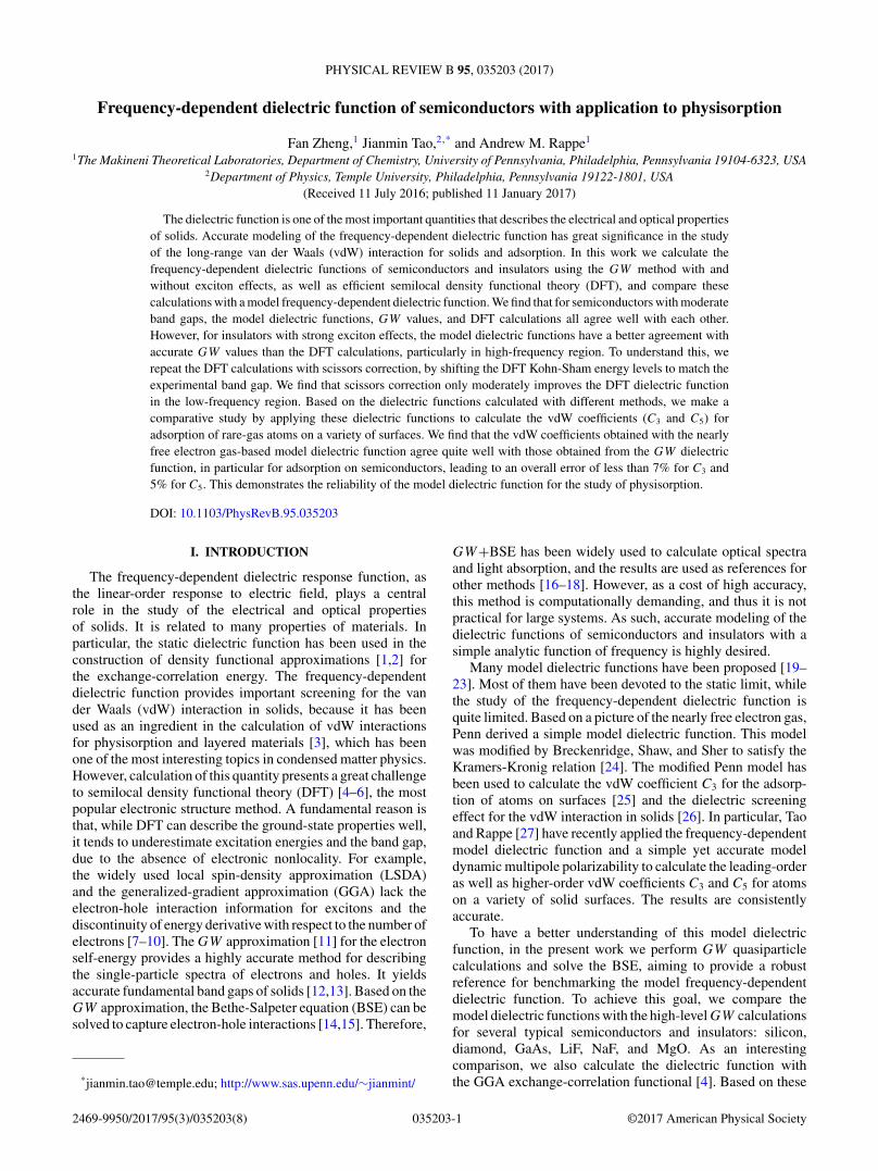
TABLE I. Experimental band gaps (fundamental), DFT scissorsband gap corrections (�corr = Eexpt
g − EDFTg ), effective energy gaps
(ωg) of the model dielectric function, and dielectric constants (ε0) ofthe model dielectric function, DFT, and GW+BSE. Here the effectiveband gaps of C, LiF, NaF, and MgO are computed via Eq. (2). Thisequation yields the effective band gaps of 4.9 and 4.6 eV for Si andGaAs, respectively, which are close to the values from the references.
Si GaAs C LiF NaF MgO
Eexptg (eV) 1.17a 1.52a 5.48a 14.20a 11.70b 7.83a
�corr (eV) 0.49 1.12 1.21 5.20 5.58 3.27
ωg (eV) 4.8c 4.3a 13.0d 23.3d 20.5d 15.5d
εexpt0 12.0a 11.3a 5.9a 1.9a 1.7e 3.0a
εmodel0 9.8 8.9 4.4 1.6 1.5 2.3
εDFT0 15.4 11.0 6.6 2.5 2.3 4.1
εDFT+sci.0 13.6 8.1 5.7 2.1 1.9 3.5
εGW0 11.5 10.7 5.1 1.8 1.6 2.6
εGW+BSE0 12.7 11.0 5.7 1.9 1.7 2.9
aReference [29].bReference [71].cReference [24].dObtained from Eq. (2).eReference [22].
they can be extracted from experimental optical data [25]. Onthe other hand, comparison of the calculated static dielectricfunction to experiment is indicative of the accuracy of thecalculated frequency dependence.
Table I shows the calculated and experimental staticdielectric functions of several semiconductors and insulators.The effective energy gaps derived from the static dielectricfunctions are also listed in Table I. From Table I we can observethat the GW+BSE static dielectric functions agree verywell with experiments for all the materials considered, whilethe GW values have better agreement with experiments forsemiconductors than for insulators, due to the strong excitoneffect in insulators [67]. Table I also shows that DFT tendsto overestimate the static dielectric function, in particular forinsulators. This overestimate was also observed in the adiabaticlocal density approximation within the time-dependent DFTformalism [68–70]. However, as shown in Table I, a scissorscorrection cannot cure this overestimate tendency problem. Weattribute this problem to the lack of electronic nonlocality ofsemilocal DFT. The frequency-dependent dielectric functionfor each material is discussed below.
B. Silicon
Figure 1 shows [ε1(iu) − 1]/[ε1(iu) + 1] of Si semicon-ductor calculated with the DFT-GGA, DFT+scissor correc-tion, GW,GW+BSE, and the model dielectric function ofEq. (3). The DFT calculated band gap is 0.62 eV, whichsignificantly underestimates the experimental band gap by0.55 eV. The experimental static dielectric constant is 11.7,which is reproduced by GW+BSE calculations (Table I).From Fig. 1, DFT gives quite accurate description of opticalresponse in terms of (ε1 − 1)/(ε1 + 1), although it givesslightly higher dielectric constant than GW+BSE at zerofrequency. At low frequencies, the model dielectric function
035203-3

FAN ZHENG, JIANMIN TAO, AND ANDREW M. RAPPE PHYSICAL REVIEW B 95, 035203 (2017)
FIG. 1. [ε1(iu) − 1]/[ε1(iu) + 1] of silicon with respect to fre-quency u (in hartree) calculated from DFT, DFT+scissors correction,GW, GW+BSE, and model dielectric function.
underestimates the GW value. This underestimate is due tothe error in the effective energy gap ωg [24], which is slightlyoverestimated. Nevertheless, the model dielectric functionagrees with GW+BSE results quite well, particularly in thehigh-frequency region.
C. GaAs
Figure 2 shows the computed dielectric functions of GaAs.GW and GW+BSE show very similar dielectric functions,indicating the weak exciton effect in GaAs [72], and strongdielectric screening effect. DFT and model dielectric functionsslightly underestimate GW+BSE values, which is because ofthe higher absorption calculated with GW and GW+BSE thanthat with DFT. In general, similar to silicon, all the methodsyield dielectric functions close to each other, in particular inthe high-frequency region. This similarity is largely due tothe fact that both semiconductors have similar band gaps anddielectric constants, as shown in Table I.
FIG. 2. [ε1(iu) − 1]/[ε1(iu) + 1] of GaAs with respect to fre-quency u (in hartree) calculated from DFT, DFT+scissors correction,GW, GW+BSE, and model dielectric function.
FIG. 3. [ε1(iu) − 1]/[ε1(iu) + 1] of diamond with respect to fre-quency u (in hartree) calculated from DFT, DFT+scissors correction,GW,GW+BSE, and model dielectric function.
D. Diamond
The dielectric function of diamond is shown in Fig. 3.Diamond shares similar geometric and electronic structureswith silicon, but with much larger band gap. In this case,the overestimation of dielectric function from DFT and theunderestimation from model dielectric function are morepronounced than those for silicon at low frequencies. Thisdifference is mainly due to the discrepancy between the Pennmodel effective band gap (slightly overestimated) and theGW or GW+BSE value. However, as energy increases tothe high-energy region, this discrepancy vanishes, matchingthe model dielectric function to GW+BSE results very well.
E. LiF
LiF is a prototypical material with strong exciton effecton its optical absorption [73]. As shown in Fig. 4, at lowenergies, GW+BSE including electron-hole interaction yieldsa higher value compared to the dielectric function withoutelectron-hole interaction, which corresponds to the exciton
FIG. 4. [ε1(iu) − 1]/[ε1(iu) + 1] of LiF with respect to fre-quency u (in hartree) calculated from DFT, DFT+scissors correction,GW,GW+BSE, and model dielectric function.
035203-4
FREQUENCY-DEPENDENT DIELECTRIC FUNCTION OF . . . PHYSICAL REVIEW B 95, 035203 (2017)
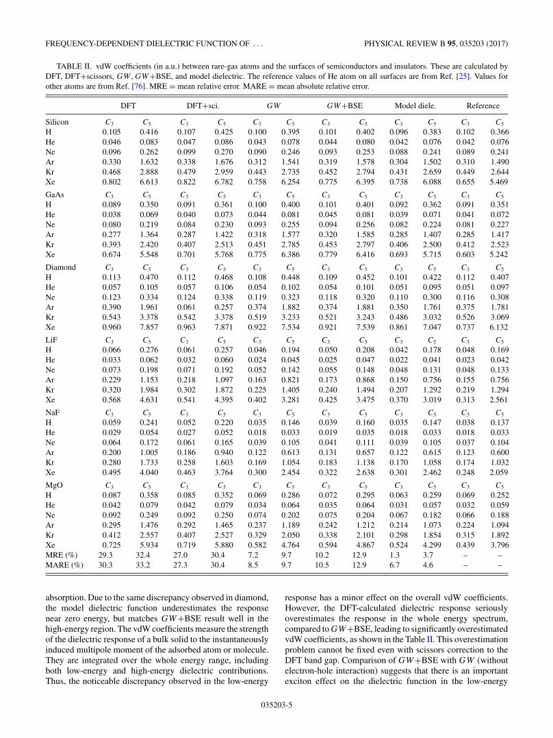
TABLE II. vdW coefficients (in a.u.) between rare-gas atoms and the surfaces of semiconductors and insulators. These are calculated byDFT, DFT+scissors, GW,GW+BSE, and model dielectric. The reference values of He atom on all surfaces are from Ref. [25]. Values forother atoms are from Ref. [76]. MRE = mean relative error. MARE = mean absolute relative error.
DFT DFT+sci. GW GW+BSE Model diele. Reference
Silicon C3 C5 C3 C5 C3 C5 C3 C5 C3 C5 C3 C5
H 0.105 0.416 0.107 0.425 0.100 0.395 0.101 0.402 0.096 0.383 0.102 0.366He 0.046 0.083 0.047 0.086 0.043 0.078 0.044 0.080 0.042 0.076 0.042 0.076Ne 0.096 0.262 0.099 0.270 0.090 0.246 0.093 0.253 0.088 0.241 0.089 0.241Ar 0.330 1.632 0.338 1.676 0.312 1.541 0.319 1.578 0.304 1.502 0.310 1.490Kr 0.468 2.888 0.479 2.959 0.443 2.735 0.452 2.794 0.431 2.659 0.449 2.644Xe 0.802 6.613 0.822 6.782 0.758 6.254 0.775 6.395 0.738 6.088 0.655 5.469
GaAs C3 C5 C3 C5 C3 C5 C3 C5 C3 C5 C3 C5
H 0.089 0.350 0.091 0.361 0.100 0.400 0.101 0.401 0.092 0.362 0.091 0.351He 0.038 0.069 0.040 0.073 0.044 0.081 0.045 0.081 0.039 0.071 0.041 0.072Ne 0.080 0.219 0.084 0.230 0.093 0.255 0.094 0.256 0.082 0.224 0.081 0.227Ar 0.277 1.364 0.287 1.422 0.318 1.577 0.320 1.585 0.285 1.407 0.285 1.417Kr 0.393 2.420 0.407 2.513 0.451 2.785 0.453 2.797 0.406 2.500 0.412 2.523Xe 0.674 5.548 0.701 5.768 0.775 6.386 0.779 6.416 0.693 5.715 0.603 5.242
Diamond C3 C5 C3 C5 C3 C5 C3 C5 C3 C5 C3 C5
H 0.113 0.470 0.112 0.468 0.108 0.448 0.109 0.452 0.101 0.422 0.112 0.407He 0.057 0.105 0.057 0.106 0.054 0.102 0.054 0.101 0.051 0.095 0.051 0.097Ne 0.123 0.334 0.124 0.338 0.119 0.323 0.118 0.320 0.110 0.300 0.116 0.308Ar 0.390 1.961 0.061 0.257 0.374 1.882 0.374 1.881 0.350 1.761 0.375 1.781Kr 0.543 3.378 0.542 3.378 0.519 3.233 0.521 3.243 0.486 3.032 0.526 3.069Xe 0.960 7.857 0.963 7.871 0.922 7.534 0.921 7.539 0.861 7.047 0.737 6.132
LiF C3 C5 C3 C5 C3 C5 C3 C5 C3 C5 C3 C5
H 0.066 0.276 0.061 0.257 0.046 0.194 0.050 0.208 0.042 0.178 0.048 0.169He 0.033 0.062 0.032 0.060 0.024 0.045 0.025 0.047 0.022 0.041 0.023 0.042Ne 0.073 0.198 0.071 0.192 0.052 0.142 0.055 0.148 0.048 0.131 0.048 0.133Ar 0.229 1.153 0.218 1.097 0.163 0.821 0.173 0.868 0.150 0.756 0.155 0.756Kr 0.320 1.984 0.302 1.872 0.225 1.405 0.240 1.494 0.207 1.292 0.219 1.294Xe 0.568 4.631 0.541 4.395 0.402 3.281 0.425 3.475 0.370 3.019 0.313 2.561
NaF C3 C5 C3 C5 C3 C5 C3 C5 C3 C5 C3 C5
H 0.059 0.241 0.052 0.220 0.035 0.146 0.039 0.160 0.035 0.147 0.038 0.137He 0.029 0.054 0.027 0.052 0.018 0.033 0.019 0.035 0.018 0.033 0.018 0.033Ne 0.064 0.172 0.061 0.165 0.039 0.105 0.041 0.111 0.039 0.105 0.037 0.104Ar 0.200 1.005 0.186 0.940 0.122 0.613 0.131 0.657 0.122 0.615 0.123 0.600Kr 0.280 1.733 0.258 1.603 0.169 1.054 0.183 1.138 0.170 1.058 0.174 1.032Xe 0.495 4.040 0.463 3.764 0.300 2.454 0.322 2.638 0.301 2.462 0.248 2.059
MgO C3 C5 C3 C5 C3 C5 C3 C5 C3 C5 C3 C5
H 0.087 0.358 0.085 0.352 0.069 0.286 0.072 0.295 0.063 0.259 0.069 0.252He 0.042 0.079 0.042 0.079 0.034 0.064 0.035 0.064 0.031 0.057 0.032 0.059Ne 0.092 0.249 0.092 0.250 0.074 0.202 0.075 0.204 0.067 0.182 0.066 0.188Ar 0.295 1.476 0.292 1.465 0.237 1.189 0.242 1.212 0.214 1.073 0.224 1.094Kr 0.412 2.557 0.407 2.527 0.329 2.050 0.338 2.101 0.298 1.854 0.315 1.892Xe 0.725 5.934 0.719 5.880 0.582 4.764 0.594 4.867 0.524 4.299 0.439 3.796MRE (%) 29.3 32.4 27.0 30.4 7.2 9.7 10.2 12.9 1.3 3.7 – –MARE (%) 30.3 33.2 27.3 30.4 8.5 9.7 10.5 12.9 6.7 4.6 – –
absorption. Due to the same discrepancy observed in diamond,the model dielectric function underestimates the responsenear zero energy, but matches GW+BSE result well in thehigh-energy region. The vdW coefficients measure the strengthof the dielectric response of a bulk solid to the instantaneouslyinduced multipole moment of the adsorbed atom or molecule.They are integrated over the whole energy range, includingboth low-energy and high-energy dielectric contributions.Thus, the noticeable discrepancy observed in the low-energy
response has a minor effect on the overall vdW coefficients.However, the DFT-calculated dielectric response seriouslyoverestimates the response in the whole energy spectrum,compared to GW+BSE, leading to significantly overestimatedvdW coefficients, as shown in the Table II. This overestimationproblem cannot be fixed even with scissors correction to theDFT band gap. Comparison of GW+BSE with GW (withoutelectron-hole interaction) suggests that there is an importantexciton effect on the dielectric function in the low-energy
035203-5

FAN ZHENG, JIANMIN TAO, AND ANDREW M. RAPPE PHYSICAL REVIEW B 95, 035203 (2017)
FIG. 5. [ε1(iu) − 1]/[ε1(iu) + 1] of NaF with respect to fre-quency u (in hartree) calculated from DFT, DFT+scissors correction,GW, GW+BSE, and model dielectric function.
range. However, semilocal DFT cannot fully capture thisexciton effect. As a result, semilocal DFT tends to overestimatethe dielectric function, although it slightly underestimates thedielectric function for semiconductors.
F. NaF
NaF is another prototypical material with strong excitoneffects. Figure 5 shows the comparison of the dielectricfunction evaluated with all the methods discussed above.From Fig. 5 we observe that the model dielectric functionstill underestimates the response near zero frequency, but withoverall good quality matching of GW+BSE results. However,semilocal DFT and scissors-corrected semilocal DFT stronglyoverestimate the dielectric function magnitude for the wholefrequency range, reflecting the inadequacy of semilocal DFT,as observed in other ionic solids.
G. MgO
As a support for variety of catalytic reactions [74,75],MgO has attracted great attention in recent years. Accuratecalculation of the dielectric function for the vdW interactionis significantly important for the prediction of the correctchemical reaction path and energy barrier. As shown inFig. 6, MgO also shows strong exciton effect, leading toobvious but less pronounced deviation of the DFT curve fromthe GW+BSE calculation, compared to other ionic solidsconsidered here. On the other hand, the model dielectricfunction agrees with GW+BSE values rather well.
H. vdW coefficients for adsorption on surfaces of solids
The vdW coefficients C3 and C5 can be calculated fromEq. (8) with the model dynamic multipole polarizability givenby [54]
αl(iu) = 2l + 1
4πdl
∫ Rl
0dr4πr2 r2l−2d4
l ω2l
d4l ω2
l + u2, (9)
where Rl is the effective vdW radius and dl is a parameterintroduced to satisfy the exact zero- and high-frequency limits.
FIG. 6. [ε1(iu) − 1[/[ε1(iu) + 1] of MgO with respect to fre-quency u (in hartree) calculated from DFT, DFT+scissors correction,GW,GW+BSE, and model dielectric function.
Numerical tests show that the model can generate vdWcoefficients for diverse atom pairs in excellent agreementwith accurate reference values, with mean absolute relativeerror of only 3% [54]. To benchmark our model dielectricfunction for adsorption, we calculate the vdW coefficients withseveral dielectric functions obtained from GW,GW+BSE,and DFT-GGA methods, and compare them to the vdWcoefficients obtained from the model dielectric function andaccurate reference values. The results are shown in Table II.
From Table II we observe that the vdW coefficientscalculated from the model dielectric function are close tothe reference values. They agree quite well with the GW
and GW+BSE values, with mean absolute relative deviationsof 2% for C3 and 5% C5 from those calculated with theGW dielectric function, and 4% for C3 and 8% for C5
from those evaluated with the GW+BSE dielectric function,respectively. The strong exciton observed in ionic solids LiF,NaF, and MgO has some effect on the vdW coefficients.But this effect is relatively small for the vdW coefficientsevaluated with GW and GW+BSE dielectric function, asthe dielectric enhancement by excitons only appears withinsmall frequency range. The model dielectric function can alsoaccount for excitons via the static dielectric function part.The vdW coefficients evaluated from the model dielectricfunction agree reasonably well with these two ab initio values,even for materials with strong exciton effect, as found inthe ionic solids considered here. However, we find that theDFT-GGA significantly overestimates vdW coefficients by30% for C3 and 33% for C5, due to the overestimation of thedielectric functions in the whole frequency range. Moreover,scissors correction to the DFT dielectric function shows littleimprovement of vdW coefficient. The detailed vdW results canbe found from Table II.
IV. CONCLUSION
In summary, we have calculated the frequency-dependentdielectric function of semiconductors and insulators with theDFT-GGA, GW , and GW+BSE methods. Based on thesecalculations, we study the accuracy of the modified Penn
035203-6
FREQUENCY-DEPENDENT DIELECTRIC FUNCTION OF . . . PHYSICAL REVIEW B 95, 035203 (2017)
model by comparing the model dielectric function to the highlyaccurate GW and GW+BSE methods. We find that the modeldielectric function agrees quite well with these two methods,in particular for small energy-gap semiconductors. However,a noticeable discrepancy arises for larger band gap materials.A similar trend has been also observed with the DFT-GGAdielectric function, which shows even greater disagreementwith the GW and GW+BSE methods, compared to the modeldielectric function. To have a better understanding of theDFT-GGA method, we adjust the GGA band gap up to theexperimental value (scissors correction). We find that thisadjustment does improve the agreement of DFT-GGA withthe benchmark methods, but the improvement is not nearlyenough. Then we calculate the vdW coefficients C3 and C5 foratoms on the surface of semiconductors and insulators withthe model dynamic multipole polarizability and the dielectricfunctions obtained from the modified Penn model, DFT-GGA,GW , and GW+BSE methods. The results show that, exceptfor the vdW coefficients obtained with the DFT-GGA dielectricfunction, they all agree well with each other. The deviationsof the vdW coefficients obtained with the model dielectric
function from those obtained with the GW+BSE dielectricfunction are 4% for C3 and 8% for C5, respectively. Thedeviation is even smaller between the vdW coefficients ob-tained from the model dielectric function and the GW method.However, these deviations become significantly larger for theDFT-GGA (C3: 29%, C5: 29%) or scissor-corrected (C3: 24%,C5: 24%) dielectric function, suggesting the significance ofelectronic nonlocality that is missing in semilocal DFT. Thissignificantly affects the performance of semilocal DFT for thedielectric function of ionic solids with strong exciton effect.
ACKNOWLEDGMENTS
F.Z. acknowledges support from NSF under Grant No.DMR-1124696. J.T. acknowledges support from NSF underGrant No. CHE-1640584 and the Office of Naval Researchunder Grant No. N00014-14-1-0761. A.M.R. was supportedby the Department of Energy Office of Basic Energy Sciences,under Grant No. DE-FG02-07ER15920. Computational sup-port was provided by the HPCMO and the NERSC.
[1] M. A. L. Marques, J. Vidal, M. J. T. Oliveira, L. Reining, and S.Botti, Phys. Rev. B 83, 035119 (2011).
[2] J. H. Skone, M. Govoni, and G. Galli, Phys. Rev. B 89, 195112(2014).
[3] A. K. Geim and I. V. Grigorieva, Nature (London) 499, 419(2013).
[4] J. P. Perdew, K. Burke, and M. Ernzerhof, Phys. Rev. Lett. 77,3865 (1996).
[5] J. Tao, J. P. Perdew, V. N. Staroverov, and G. E. Scuseria, Phys.Rev. Lett. 91, 146401 (2003).
[6] J. Tao and Y. Mo, Phys. Rev. Lett. 117, 073001 (2016).[7] J. P. Perdew and M. Levy, Phys. Rev. Lett. 51, 1884 (1983).[8] L. J. Sham and M. Schluter, Phys. Rev. Lett. 51, 1888 (1983).[9] J. Janak, Phys. Rev. B 18, 7165 (1978).
[10] J. P. Perdew, R. G. Parr, M. Levy, and J. L. Balduz Jr, Phys. Rev.Lett. 49, 1691 (1982).
[11] L. Hedin, Phys. Rev. 139, A796 (1965).[12] X. Zhu and S. G. Louie, Phys. Rev. B 43, 14142 (1991).[13] G. Onida, L. Reining, and A. Rubio, Rev. Mod. Phys. 74, 601
(2002).[14] G. Onida, L. Reining, R. W. Godby, R. Del Sole, and W.
Andreoni, Phys. Rev. Lett. 75, 818 (1995).[15] M. Rohlfing and S. G. Louie, Phys. Rev. Lett. 81, 2312 (1998).[16] A. Schleife, C. Rodl, F. Fuchs, J. Furthmuller, and F. Bechstedt,
Phys. Rev. B 80, 035112 (2009).[17] H. C. Hsueh, G. Y. Guo, and S. G. Louie, Phys. Rev. B 84,
085404 (2011).[18] D. Y. Qiu, F. H. da Jornada, and S. G. Louie, Phys. Rev. Lett.
111, 216805 (2013).[19] D. R. Penn, Phys. Rev. 128, 2093 (1962).[20] D. R. Penn, Phys. Rev. B 35, 482 (1987).[21] Z. H. Levine and S. G. Louie, Phys. Rev. B 25, 6310 (1982).[22] M. Lines, Phys. Rev. B 41, 3372 (1990).[23] C. C. Kim, J. W. Garland, H. Abad, and P. M. Raccah, Phys.
Rev. B 45, 11749 (1992).
[24] R. A. Breckenridge, R. W. Shaw Jr, and A. Sher, Phys. Rev. B10, 2483 (1974).
[25] G. Vidali and M. W. Cole, Surf. Sci. Lett. 107, L374 (1981).[26] J. Tao, J. Yang, and A. M. Rappe, J. Chem. Phys. 142, 164302
(2015).[27] J. Tao and A. M. Rappe, Phys. Rev. Lett. 112, 106101 (2014).[28] Z. H. Levine and D. C. Allan, Phys. Rev. Lett. 63, 1719
(1989).[29] J. A. Van Vechten, Phys. Rev. 182, 891 (1969).[30] H. R. Philipp and H. Ehrenreich, Phys. Rev. Lett. 8, 92 (1962).[31] H. R. Philipp and H. Ehrenreich, Phys. Rev. 129, 1550 (1963).[32] M. D. Sturge, Phys. Rev. 127, 768 (1962).[33] R. Willardsen and A. Beer, Semiconductors and Semimetals
(Academic, New York, 1981), Vol. 3.[34] P. Giannozzi, S. Baroni, N. Bonini, M. Calandra, R. Car, C.
Cavazzoni, D. Ceresoli, G. L. Chiarotti, M. Cococcioni, I.Dabo, A. D. Corso, S. de Gironcoli, S. Fabris, G. Fratesi, R.Gebauer, U. Gerstmann, C. Gougoussis, A. Kokalj, M. Lazzeri,L. Martin-Samos, N. Marzari, F. Mauri, R. Mazzarello, S.Paolini, A. Pasquarello, L. Paulatto, C. Sbraccia, S. Scandolo,G. Sclauzero, A. P. Seitsonen, A. Smogunov, P. Umari, and R.M. Wentzcovitch, J. Phys. Condens. Matter 21, 395502 (2009).
[35] A. M. Rappe, K. M. Rabe, E. Kaxiras, and J. D. Joannopoulos,Phys. Rev. B 41, 1227 (1990).
[36] N. J. Ramer and A. M. Rappe, Phys. Rev. B 59, 12471 (1999).[37] M. Shishkin and G. Kresse, Phys. Rev. B 75, 235102 (2007).[38] F. Nastos, B. Olejnik, K. Schwarz, and J. E. Sipe, Phys. Rev. B
72, 045223 (2005).[39] M. S. Hybertsen and S. G. Louie, Phys. Rev. B 34, 5390 (1986).[40] M. Rohlfing and S. G. Louie, Phys. Rev. B 62, 4927 (2000).[41] J. Deslippe, G. Samsonidze, D. A. Strubbe, M. Jain, M. L.
Cohen, and S. G. Louie, Comput. Phys. Commun. 183, 1269(2012).
[42] B. D. Malone and M. L. Cohen, J. Phys. Condens. Matter 25,105503 (2013).
035203-7

FAN ZHENG, JIANMIN TAO, AND ANDREW M. RAPPE PHYSICAL REVIEW B 95, 035203 (2017)
[43] M. Dion, H. Rydberg, E. Schroder, D. C. Langreth, and B. I.Lundqvist, Phys. Rev. Lett. 92, 246401 (2004).
[44] J. Granatier, P. Lazar, M. Otyepka, and P. Hobza, J. Chem.Theory. Comput. 7, 3743 (2011).
[45] J. Klimes, D. R. Bowler, and A. Michaelides, Phys. Rev. B 83,195131 (2011).
[46] P. Lazic, Z. Crljen, R. Brako, and B. Gumhalter, Phys. Rev. B72, 245407 (2005).
[47] D.-L. Chen, W. Al-Saidi, and J. K. Johnson, J. Phys. Condens.Matter 24, 424211 (2012).
[48] S. Grimme, J. Comput. Chem. 25, 1463 (2004).[49] A. D. Becke and E. R. Johnson, J. Chem. Phys. 127, 154108
(2007).[50] A. Tkatchenko and M. Scheffler, Phys. Rev. Lett. 102, 073005
(2009).[51] P. L. Silvestrelli, Phys. Rev. Lett. 100, 053002 (2008).[52] A. Tkatchenko, A. Ambrosetti, and R. A. DiStasio Jr, J. Chem.
Phys. 138, 074106 (2013).[53] J. Tao, J. P. Perdew, and A. Ruzsinszky, Phys. Rev. B 81, 233102
(2010).[54] J. Tao, J. P. Perdew, and A. Ruzsinszky, Proc. Natl. Acad. Sci.
USA 109, 18 (2012).[55] J. Tao and J. P. Perdew, J. Chem. Phys. 141, 141101 (2014).[56] J. Tao and A. M. Rappe, J. Chem. Phys. 144, 031102 (2016).[57] S. Grimme, J. Antony, S. Ehrlich, and H. Krieg, J. Chem. Phys.
132, 154104 (2010).[58] S. Grimme, J. Comput. Chem. 27, 1787 (2006).[59] V. G. Ruiz, W. Liu, E. Zojer, M. Scheffler, and A. Tkatchenko,
Phys. Rev. Lett. 108, 146103 (2012).[60] J. Ma, A. Michaelides, D. Alfe, L. Schimka, G. Kresse, and E.
Wang, Phys. Rev. B 84, 033402 (2011).[61] H. Fang, P. Kamakoti, J. Zang, S. Cundy, C. Paur, P. I.
Ravikovitch, and D. S. Sholl, J. Phys. Chem. C 116, 10692(2012).
[62] T. Sirtl, J. Jelic, J. Meyer, K. Das, W. M. Heckl, W. Moritz, J.Rundgren, M. Schmittel, K. Reuter, and M. Lackinger, Phys.Chem. Chem. Phys. 15, 11054 (2013).
[63] M. W. Schmidt, K. K. Baldridge, J. A. Boatz, S. T. Elbert, M. S.Gordon, J. H. Jensen, S. Koseki, N. Matsunaga, K. A. Nguyen,S. J. Su, T. L. Windus, M. Dupuis, and J. A. Montgomery, J.Comput. Chem. 14, 1347 (1993).
[64] C. Dykstra, G. Frenking, K. Kim, and G. Scuseria, Theory andApplications of Computational Chemistry: The First Forty Years(Elsevier, Amsterdam, 2011).
[65] D. Dalvit, P. Milonni, D. Roberts, and F. d. Rosa, CasimirPhysics (Springer, Berlin, 2011).
[66] E. Zaremba and W. Kohn, Phys. Rev. B 13, 2270 (1976).[67] Z.-h. Yang, F. Sottile, and C. A. Ullrich, Phys. Rev. B 92, 035202
(2015).[68] W. G. Aulbur, L. Jonsson, and J. W. Wilkins, Solid State Physics
(Elsevier, Amsterdam, 1999), pp. 1–218.[69] M. van Faassen, P. L. de Boeij, R. van Leeuwen, J. A. Berger,
and J. G. Snijders, Phys. Rev. Lett. 88, 186401 (2002).[70] M. van Faassen, P. L. de Boeij, R. van Leeuwen, J. A. Berger,
and J. G. Snijders, J. Chem. Phys. 118, 1044 (2003).[71] R. Poole, J. Jenkin, J. Liesegang, and R. Leckey, Phys. Rev. B
11, 5179 (1975).[72] S. B. Nam, D. C. Reynolds, C. W. Litton, R. J. Almassy, T. C.
Collins, and C. M. Wolfe, Phys. Rev. B 13, 761 (1976).[73] P. Abbamonte, T. Graber, J. P. Reed, S. Smadici, C.-L. Yeh, A.
Shukla, J.-P. Rueff, and W. Ku, Proc. Natl. Acad. Sci. USA 105,12159 (2008).
[74] C. Zhang, B. Yoon, and U. Landman, J. Am. Chem. Soc. 129,2228 (2007).
[75] B. Yoon, H. Hakkinen, U. Landman, A. S. Worz, J. M.Antonietti, S. Abbet, K. Judai, and U. Heiz, Science 307, 403(2005).
[76] G. Vidali and M. W. Cole, Surf. Sci. 110, 10 (1981).
035203-8