Embed Size (px)
Citation preview

1
Free-standingFree-standingFree-standingFree-standing GrapheneGrapheneGrapheneGraphene bybybyby ScanningScanningScanningScanning TransmissionTransmissionTransmissionTransmission ElectronElectronElectronElectronMicroscopyMicroscopyMicroscopyMicroscopy
F. Song 1, 2, Z.Y. Li 1 *, Z.W. Wang 1, L. He 2, M. Han 2 and G.H. Wang 2
1 Nanoscale Physics Research Laboratory, School of Physics and Astronomy, University of
Birmingham, Birmingham B15 2TT, UK
2 National Laboratory of Solid State Microstructures, Nanjing University, Nanjing 210093, China
AbstractAbstractAbstractAbstract
Free-standing graphene sheets have been imaged by scanning transmission electron microscopy
(STEM). We show that the discrete numbers of graphene layers enable an accurate calibration of
STEM intensity to be performed over an extended thickness and with single atomic layer sensitivity.
We have applied this calibration to carbon nanoparticles with complex structure. This leads to the
direct and accurate measurement of the electron mean free path. Here, we demonstrate potentials
using graphene sheets as a novel mass standard in the STEM-based mass spectrometry.
KEYWORDSKEYWORDSKEYWORDSKEYWORDS: graphene, carbon nanoparticles, Scanning Transmission Electron Microscopy
* Corresponding author. [email protected]

2
1.1.1.1. IntroductionIntroductionIntroductionIntroduction
Scanning transmission electron microscopy (STEM) has become an indispensable tool in
many fields of science community, including physics, materials, biology and nanotechnology [1-6].
For example, in structural biology, the ability of STEM in three-dimensional mass mapping of large
protein assemblies often provides invaluable input in structural model building [7]. There are two
approaches using STEM to obtain accurate mass mapping, absolute and relative measurements. The
former involves an extensive calibration of the operational parameters of the microscope that is
very difficult to carry out accurately and requires additional hardware to be fit into the microscope,
hence the approach has only been taken up by a few dedicated groups worldwide until now [8-10].
A simpler approach is the measurement of electron scattering cross section using a mass standard
[5]. A common mass standard used in structural biology is a hollow cylindrical shaped tobacco
mosaic virus (TMV). They are about 300 nm in length and about 18 nm in diameter with an inner
channel of ~4 nm. The problem for TMV mass standard is not only its poor accuracy, but also mass
loss due to radiation damage or mass gain due to filling of central cavity [5]. These drawbacks
could affect the precision of mass measurements. Recently, size-selected gold clusters have been
applied to serve as a convenient mass standard for nanoparticles [11]. This has opened an
alternative avenue for a quick and easy way of weighing nanoparticles on supports and gaining
insight into their fine structure and shapes. In principle, this method could be extended to include all
elements. However, practically this is difficult for light elements, since STEM intensity is
proportional to , where Z is atomic number of the elements and α is in the range of 1.5-1.9
Za
depending on the detector collection angle, sample thickness, and the Debye-Waller factor of the
atomic species [1,12,13]. As a result, the light elements would have a much weaker image contrast
than that of heavy elements.
In this study, we propose an alternative mass standard using free-standing graphene [14,15]
sheets for light element mass measurements in STEM. We show that the discrete numbers of
graphene layers enable an accurate calibration of STEM intensity to be performed. As an example

3
of applications, we have applied the calibrated STEM intensity from graphene layers to gain insight
of carbon nanoparticles of complex structure.
2.2.2.2. MaterialsMaterialsMaterialsMaterials andandandand MethodsMethodsMethodsMethods
2.12.12.12.1 PreparationPreparationPreparationPreparation andandandand transfertransfertransfertransfer ofofofof graphenegraphenegraphenegraphene flakesflakesflakesflakes
To prepare thin graphene sheets, we used the established procedures of micromechanical
patterning followed by repetitive cleavage of a highly-ordered-pyrolytic-graphite (HOPG) [14,16].
Patterned HOPG flakes were first pressed on a glass slide with a photo resistive spun of 0.5 µm
thickness. After heating the sample at 110°C for 30 minutes, the visible flakes were removed. The
remaining HOPG on the glass slide was peeled by a scotch tape for more than 40 times, and the
remainders were then transferred to an acetone bath. The solution containing graphene flakes was
drop casting on a holey Formvar filmed grid (XXBR customized TEM support). Once the acetone
was evaporated, the graphene flakes would be held on the grid. To achieve a large density of the
captured graphene flakes (10-100 pieces/cm-2), the procedure was repeated over 10 times.
2.22.22.22.2 CarbonCarbonCarbonCarbon nanoparticlesnanoparticlesnanoparticlesnanoparticles
The carbon nanoparticles were prepared by plasma sputtering. In a radiofrequency
sputtering chamber, 20 sccm of Ar was introduced with the final pressure of 18 Pa. The net input
power was 400 W for a microcrystalline graphite target of 2 inches in diameter. The carbon
particles were deposited on a Formvar filmed grid through a small nozzle, through which a
differential pumping (20 Pa - 10-3 Pa) was applied. The Ar pressure can be adjusted to control the
morphology of carbon nanoparticles [17,18].
3.3.3.3. ResultsResultsResultsResults andandandand DiscussionDiscussionDiscussionDiscussion
FigureFigureFigureFigure 1111 displays a representative overview, by STEM imaging, of the graphene sheets,
highlighted by light blue shade. The image was taken in a 200 KV Tecnai F20 STEM fitted with a
high angle annular dark field (HAADF) detector. Here, large areas with uniformed STEM contrast

4
strongly suggest the uniform thickness of graphene flakes prepared in this study. The variation of
the intensity between the uniform areas gives clear indication that the graphene sheets in that region
are folded or stacked together.
To establish direct correlation between the STEM intensity with the number of layers in
graphene sheets, we apply an independent layer counting method by utilizing dark lines in bright
field TEM images at the edge of graphene sheets. It has been demonstrated previously by several
groups that edges and folding of a few layers (1, 2 and 4) of freely suspending graphene sheets are
dominated by corresponding numbers of dark lines in TEM images [19-23]. The validity of this
method has been cross-checked using Raman spectrum [19, 24, 25], nanobeam electron diffraction
[21] and electron energy loss spectroscopy [22, 23]. To quantify the layer thickness of our
graphene sheets, we searched over a large area of the sample for the freely suspending graphene
sheets (for example, the area indicated by the arrows in Fig. 1). FigFigFigFigureureureure 2222 (a,(a,(a,(a, b)b)b)b) displays two typical
examples of such edges with thickness of 3 and 10 layers, respectively, in high-resolution bright
field imaging. Care needs to be taken to discern Fresnel fringes from the graphene edges. One may
see the image in Fig. 2(a) is in focus and presents rather poor contrast. This guarantees the accurate
layer counting of the sample. On the contratry, the image in Fig.2(b) is a bit underfocus, leading to
quite better contrast. Crossing of the two defocused fringes introduces the error of 1 layer. The
STEM images taken from the corresponding edge area are shown in Fig.Fig.Fig.Fig. 2222 (c,(c,(c,(c, d)d)d)d). The line profiles
in Fig.Fig.Fig.Fig. 2222 (e,(e,(e,(e, f)f)f)f) across the step-edges (marked by dashed line in the STEM images) show clearly
step-wise intensity variation between vacuum and the graphene sheets.
FigureFigureFigureFigure 3(a)3(a)3(a)3(a) displays the HAADF intensity as a function of graphene layer number. A
monotonic relationship is apparent. Here, to obtain the HAADF intensity values, we examined a
relative clean area (with uniform contrast) over at least 100×100 pixels and we then plotted the
histogram of the pixel intensity distribution for that particular layer thickness. An example for a 4
layers thick area is shown in inset of Fig.Fig.Fig.Fig. 3(a)3(a)3(a)3(a). The mean value of the histogram and the standard
deviation for each individual layer thickness is shown in FigureFigureFigureFigure 3333. The error bars here include

5
contributions from both contamination and the background dark counts. It is inherently difficult to
avoid contamination completely in obtaining HAADF-STEM images. The Birmingham Tecnai
microscope is equipped with a dedicated cryo-capsule around the specimen area. This has been
shown to reduce contamination building-up rate substantially. However, sometimes during
prolonged scanning over the interested area by the focused electron beam, the gradual built-up
contamination layer would leave a visible mark when zooming out of the scanned area. If this was
the case, the data would be discounted and a new area would be studied. A close inspection of FigFigFigFig....
3333 (a)(a)(a)(a) shows that HAADF-STEM intensity fits reasonably well into a linear function through the
origin for graphene thickness up to 9 layers.
The resultant linear relation suggests that the multiple scattering is negligible in this ultra-
thin film region. This would simplify greatly the subsequent data analysis procedures, as simple
kinematical scattering models would be applicable [26]. To see how far the single scattering model
can be extended to, we have purposely searched for thick graphene sheets to image. The results are
presented in FigFigFigFig.... 3(b)3(b)3(b)3(b) together with that of thin layers shown in Fig.Fig.Fig.Fig. 3(a)3(a)3(a)3(a). It is interesting to
observe that the linear relation of the HAADF intensity persists to an exceptional large number of
layers at around 50. This value extends the range that has been reported experimentally in the
literature for the thickest graphene thin film (35 layers) [18, 22, 23], and is roughly 3 folds larger
than the linear regime found in size-selected gold clusters in terms of atomic column depth (~15
atom height) in shell structure model [11]. The latter may be attributed to the weak electron
scattering of the carbon atoms compared with gold.
The effect of camera length on the HAADF-STEM intensity has also been investigated. No
intensity reversal was observed when the camera length changes between 150-520 mm, which
corresponds to the detector’s minimum inner acceptance angle, θ, of 48-14 mrad. In the present
study, the camera length of 285 mm (θ = 25 mrad) was used to ensure that most electrons detected
are from incoherent thermal diffuse scattering while at the same time to maximize the signal to
noise ratio. Using the single electron scattering approximation [26], the electron cross-section can

6
be directly deduced from fitting the HAADF intensity-thickness relation with an exponential
function, , where d is the layer thickness, and A and ζ are fitting parameters. FigFigFigFig.... 3(b3(b3(b3(b))))
I = A 1− e−ζd( )shows a good fit over the entire investigated thickness up to 100 layers. Using the book value of
graphite layer spacing of 0.34 nm [27], we obtain the cross section and the electron mean free path
being nm2 and nm, respectively. The values are in line with what have
7.6 ±0.6( )×10−5
120 ± 9
been reported in literature for amorphous carbon and diamond [28].
The HAADF intensity vs. thickness relation in FigFigFigFig.... 3333 can be served as a carbon mass
calibration for HAADF-STEM imaging. The uncertainty of weighing the nanoobjects originates
from the interaction volume between the beam and the mass standard . The Tecnai F20 machines
provide the focused electron beam with the diameter of 0.4nm presently with the interaction
volume of 42.7*Layers Å3[11]. Considering the minimum counting uncertainty of 0.6 layers and
the bulk graphite density [28], the atomic balance achieves the optimum precision of nearly 3
carbon atoms. Here we demonstrate this application in studying carbon nanoparticles with complex
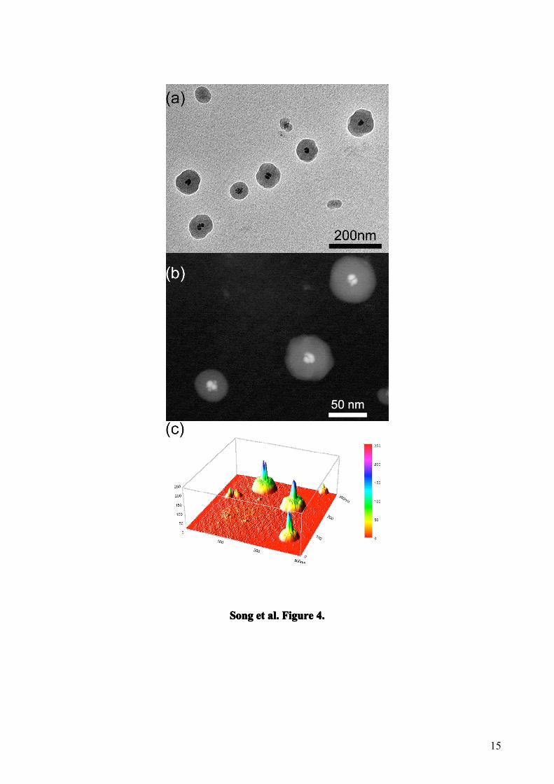
morphology. FigureFigureFigureFigure 4444 shows a typical bright field TEM image (a) and STEM image (b) of the
carbon nanoparticles produced by plasma sputtering. The images were taken using 200 KV Tecnai
F20 at Nanjing University with the comparable setting-up as for the graphene study in Birmingham.
These particles have overall spherical shape. However, STEM reveals high intensity at the centre,
though energy-dispersive X-ray spectroscopy confirms that no foreign atoms are present within the
core while electron energy loss spectroscopy (EELS) shows both the core and the shell have similar
graphite-like chemical bonding (see supplementary materials for details). Nanobeam electron
diffraction confirms that the particles are amorphous. To characterize these inhomogenous
nanoparticles, we apply the calibration curve in FigFigFigFig.... 3333. Here, the image in Fig.Fig.Fig.Fig. 4444 (b)(b)(b)(b) may be
viewed as a quasi- 3D mass density mapping of the nanoparticles, shown in Fig.Fig.Fig.Fig. 4(c)4(c)4(c)4(c) in false colour.
It is apparent that all of these particles have complicated core-shell structures, in which the core is
formed by dense nuclear seeds that are surrounded by a porous shell. The densities of the core and
shell can be obtained as g/cm3 and g/cm3, respectively. The former is close to
2.3± 0.3
0.45 ± 0.06

7
the book value of graphite density, 2.09-2.23 g/cm3 [29]. The revelation of this complex structure
of carbon nanoparticles may provide foundation for developing applications for energy storage,
such as enhancement of hydrogen adsorption (two order of magnitude higher) in vacuum condition
as compared with that of graphite. The result will be reported in a separated publication.
4.4.4.4. ConclusionsConclusionsConclusionsConclusions
In summary, we have demonstrated potentials using graphene sheets for mass standard for
light element materials in STEM based mass spectrometry. By applying this mass standard to the
carbon nanoparticles with complicated core-shell inhomogeneous morphology, we show that the
core is graphite-like carbon whiles the shell has a porous structure. Previous attempts using
conventional electron microscopy based elemental techniques such as EDX and EELS have failed
in distinguishing such a core-shell structure of the carbon nanoparticles. The advance shown in the
present study is made possible today partly due to our recent work in exploring potential in
quantification STEM analysis [2, 11] and partly due to the recent surge of interests in graphene in
the scientific community, which makes this material routinely available through various physical
and chemical preparation routes. It is envisaged that the current proposal of using graphene for
mass standard would be interesting not only for the materials scientists who work on light elements,
but also potentially for biologists as an alternative to the commonly used tobacco virus as mass
standard, in particularly for their structural investigations of low molecular weight biological
materials. As compared to our previous progress using the coarse mass standards of carbon
nanoclusters (in reference [12]) , this alternative standards has many advantages. For example, they
have nearly perfect 2D crystalline structure, their thickness can be well controlled and accurately
measured. Therefore an improved data uncertainty can be expected. They are more robust.
Potentially they can also replace the commonly used amorphous carbon thin film as the ultrathin
and quantitative TEM/STEM supports.

8
AcknowledgementsAcknowledgementsAcknowledgementsAcknowledgements
We thank Dr. Mi Yeon Song for her helpful assistance in preparing graphene samples. We
acknowledge UK Engineering and Physical Sciences Research Council for supporting this project.
The work in China is supported by the National Natural Science Foundation of China (Grant
numbers: 90606002, 10674056, and 10775070) and the National Key Projects for Basic Research
of China (Grant numbers: 2009CB930501, 2010CB923401). Supporting Information is available
online from Wiley InterScience or from the author.

9
ReferenceReferenceReferenceReference
[1] O.L. Krivanek, M.F. Chisholm, V. Nicolosi, T.J. Pennycook, G.J. Corbin, N. Dellby, M.F.
Murfitt, C.S. Own, Z.S. Szilagyi, M.P. Oxley, S. T. Pantelides, S.J. Pennycook, Nature 464 (2010)
571.
[2] Z. Y. Li, N. P. Young, M. Di Vece, S. Palomba, R. E. Palmer, A. L. Bleloch, B. C. Curley, R. L.
Johnston, J. Jiang, J. Yuan, Nature 451 (2008) 46.
[3] A. Y. Borisevich, A. R. Lupini, S. J. Pennycook, Proc. Natl. Acad. Sci. U.S.A. 103 (2006) 3044.
[4] P. R. Buseck, R. E. Dunin-Borkowski, B. Devouard, R. B. Frankel, M. R. McCartney, P. A.
Midgley, W. M. Posfai, Proc. Natl. Acad. Sci. U.S.A. 98 (2001) 13490.
[5] S. A. Muller, A. Engel, Micron 32 (2001) 21.
[6] J. S. Wall and J. F. Hainfeld, Ann. Rev. Biophys. Biophys. Chem. 15 (1986) 355.
[7] A. K. Paravastu, R. D. Leapman, W.-M. Yau, R. Tycko, Proc. Natl. Acad. Sci. U.S.A. 105
(2008) 18349.
[8] A. Singhal, J. C. Yang, J. M. Gibson, Ultramicroscopy 67 (1997) 191.
[9] J. M. Lebeau, S. D. Finflay, L. J. Allen, S. Stemmer, Phys. Rev. Lett. 100 (2008) 206101.
[10] J. M. LeBeau, S. Stemmer, Ultramicroscopy 108 (2008) 1653.
[11] N. P. Young, Z. Y. Li, Y. Chen, S. Palomba, M. D. Vece, R. E. Palmer, Phys. Rev. Lett. 101
(2008) 246103.
[12] P. Hartel, H. Rose, C. Dinges, Ultramicroscopy 63 (1996) 93.
[13] Y. M. Zhu, H. Inada, L. Wu, J. Wall, D. Su, Hitachie M News 3 (2009) 2.
[14] K. S. Novoselov, Proc. Natl. Acad. Sci. U.S.A. 102 (2005) 10451.
[15] A. K. Geim, K. S. Novoselov, Nature Materials 6 (2007) 183.
[16] J. C. Meyer, C. O. Girit, M. F. Crommie, A. Zettl, Nature 454 (2008) 319.
[17] M. Han, C. Xu, D. Zhu, L. Yang, J. Zhang, Y. Chen, D. K., F. Song, G. Wang, Adv. Mater. 19
(2007) 2979.
10
[18] F. Q. Song, X. F. Wang, R. Powles, L. B. He, N. A. Marks, S. F. Zhao, J. G. Wan, Z. W. Liu, J.
F. Zhou, S. P. Ringer, M. Han, G. H. Wang, Appl. Phys. Lett. 96 (2010) 033103.
[19] A. C. Ferrari, J. C. Meyer, V. Scardaci, C. Casiraghi, M. Lazzeri, F. Mauri, S. Piscanes, D.
Jiang, K. S. Novoselov, S. Roth, A. K. Geim, Phys. Rev. Lett. 97 (2006) 187401.
[20] Z. Liu, K. Suenaga, P. J. F. Harris, S. Iijima, Phys. Rev. Lett. 102 (2009) 015501
[21] J. C. Meyer, A. K. Geim, M. I. Katsnelson, K. S. Novoselov, T. J. Booth and S. Roth, Nature
446 (2007) 60.
[22] T. Eberlein, U. Bangert, R. R. Nair, R. Jones, M. Gass, A. L. Bleloch, K. S. Novoselov, A.
Geim and P. R. Briddon, Phys. Rev. B 77 (2008) 233406.
[23] M. Gass, U. Bangert, A. Bleloch, P. Wang, R. Nair, A. Geim, Nature Nanotech. 3 (2008) 676.
[24] Z. H. Ni, H. M. Wang, J. Kasim, H. M. Fan, T. Yu, Y. H. Wu, Y. P. Feng, Z. X. Shen, Nano
Letters 7 (2007) 2758.
[25] D. Graf, F. Molitor, K. Ensslin, C. Stampfer, A. Jungen, C. Hierold, L. Wirtz, Nano Letters 7
(2007) 238.
[26] I. Angert, C. Burmester, C. Dinges, H. Rose and R. R. Schroder, Ultramicroscopy 63 (1996)
181.
[27] A. B. Yen, B. E. Schwickert, Appl. Phys. Lett. 84 (2004) 4702.
[28] K. Iakoubovskii, K. Mitsuishi, Phys. Rev. B 77 (2008) 104102.
[29] H. H. Hsieh, Y. K. Chang, W. F. Pong, M.-H. Tsai, F. Z. Chien, P. K. Tseng, I. N. Lin, H. F.
Cheng, Appl. Phys. Lett. 75 (1999) 2229.

11
FigureFigureFigureFigure CaptionCaptionCaptionCaptionssss
FigureFigureFigureFigure 1111 HAADF-STEM image showing an overview of graphene flakes supported by holey
Formvar film covered Cu grids. The graphene are highlighted by blue shades. The bright patches on
the right side of the images are contamination left on the samples during preparation and handling
of the specimen. The arrows indicate areas where the graphene freely are suspended on the holey
film.
FigureFigureFigureFigure 2.2.2.2. GrapheneGrapheneGrapheneGraphene thicknessthicknessthicknessthickness analysis.analysis.analysis.analysis. (a, b) High-resolution TEM images of the folded graphene
edge, where the dark lines indicate the number of layers of 3 and 10 for two cases. (c, d) The
HAADF-STEM images of the corresponding areas. (e, f) The intensity line profiles averaged over a
few pixels, taken from the positions indicated in (c) and (d).
FigureFigureFigureFigure 3.3.3.3. TheTheTheThe calibrationcalibrationcalibrationcalibration curve.curve.curve.curve. (a) The HAADF intensities are plotted against the layer number
up to 9. The data and the error bars are taken from the mean value and the corresponding standard
deviation from the selected layer numbers of graphene. The linear fitting is a guide for eyes. The
inset shows an intensity histogram for a suspended 4-layer graphene. (b) An extended range of
intensity-thickness relation is fitted by the single scattering approximation (solid line):
. The linear fitting in (a) is shown here in dashed line as a comparison.
I = A 1− e−ξd( )
FigureFigureFigureFigure 4.4.4.4. ComplexComplexComplexComplex inhomogenousinhomogenousinhomogenousinhomogenous structurestructurestructurestructure ofofofof carboncarboncarboncarbon nanoparticles.nanoparticles.nanoparticles.nanoparticles. (a) TEM image of carbon
nanoparticles prepared by plasma sputtering. (b) HAADF-STEM image of the carbon particles (not
the same area as in (a) but from the same specimen). (c) The 3D view of mass mapping of
nanoparticles

12
SongSongSongSong etetetet al.al.al.al. FigureFigureFigureFigure 1111

13
SongSongSongSong etetetet al.al.al.al. FigureFigureFigureFigure 2.2.2.2.

14
SongSongSongSong etetetet al.al.al.al. FigureFigureFigureFigure 3333....
15
SongSongSongSong etetetet al.al.al.al. FigureFigureFigureFigure 4444....