Embed Size (px)
Citation preview
FPGA Message Passing
Cluster Architectures by
Eoin Creedon, B.A. (Mod.) Computer Science
Thesis Presented to the University of Dublin, Trinity College
in fulfilment of the requirements for the degree of
Doctor of Philosophy (Computer Science)
May 2010


Declaration
I, the undersigned, declare that this work has not been previously submitted to this or any other University,
and that unless otherwise stated, it is entirely my own work.
__________________________
Eoin Creedon
Dated: 26th May 2010


Permission to Lend and/or Copy
I, the undersigned, agree that Trinity College Library may lend or copy this thesis upon request.
__________________________
Eoin Creedon
Dated: 26th May 2010


FPGA Message Passing Cluster Architectures
ABSTRACT This work investigates inter-Field Programmable Gate Array (FPGA) communication mechanisms,
specifically the use of message passing and switched Ethernet communication mechanisms. Inter-FPGA
communication is required in situations where the computational demands of an algorithm cannot be satisfied
by a single FPGA. To meet the algorithms requirements, it must be implemented over several FPGAs. This
leads to the need for remote register transfer operations that allow for the exchange of data and synchronisa-
tion between aspects of the algorithm that are implemented on each individual FPGAs. The algorithm is de-
fined using a Hardware Description Language allowing it to be implemented through the reconfigurable logic
of the FPGA. This thesis argues for an implementation of the data exchange and synchronisation mecha-
nisms that facilitate remote register transfer operations in reconfigurable logic on the FPGA. This approach
allows for a definition in Hardware Description Language and therefore can provide the application pro-
grammer with a Hardware Description Language Application Programming Interface that is simple to inte-
grate into the application and hides the implementation of the communication mechanisms from the applica-
tion programmer. A message passing protocol is used to implement the remote register transfer operations.
Message passing and switched Ethernet are argued for as the approach to be taken as they support
algorithm parallelisation in a scalable and robust manner. Using the Hardware Description Language Mes-
sage Passing Application Programming Interface (HDL MP API) facilitates both the remote register transfer
operations between FPGAs and also between FPGAs and workstations. The message passing and switched
Ethernet operations can be implemented using either a dedicated hardware microarchitecture or an FPGA
processor, with the HDL MP API developed to abstract the application from which data exchange approach
is being taken. By looking at both approaches, this thesis argues for the feasibility of message passing in
conjunction with switched Ethernet as a viable platform for supporting application parallelisation across in-
terconnected FPGAs. To support this, discussions on characteristics of various parallel algorithms aid in
demonstrated which approach is suitable for a given set of algorithm requirements.
Using message passing and switched Ethernet, evaluations of both the hardware microarchitecture
and an FPGA processor have been undertaken across both 10/100 Mb and Gigabit Ethernet. The evaluations
demonstrate the feasibility of using message passing and switched Ethernet as the interconnect structures for
distributed FPGAs while also highlighting advantages for implementing the structures in hardware through
the lower latency and higher application network bandwidth that is achieved. The hardware microarchitec-
ture is able to achieve a maximum bandwidth of 1800 Mbps while the FPGA processor achieves a maximum
bandwidth of 140 Mbps. The HDL MP API has been evaluated for its functionality in supporting parallel
algorithms implemented across multiple FPGAs. Parallel Matrix Multiplication has been implemented as a
high performance algorithm that can be parallelised across the FPGAs. Experiment results show that the
HDL MP API is able to support the algorithms parallel computations across a different number of FPGAs,
depending on computational requirements.


FPGA Message Passing Cluster Architectures
ACKNOWLEDGEMENTS The work in this thesis is the culmination of a number of years of research. Firstly, I would like to thank my
supervisor Dr. Michael Manzke for his assistance throughout this research. His guidance helped refine many
different aspects of the research that was undertaken. I would also like to thank Ross Brennan, Muiris
Woulfe, Owen Callanan, Milan Tichy, Jeremy Jones and David Gregg for their assistance at different times.
I would like to thank my examiners, Peter Cheung and Stefan Weber, for an interesting and insightful viva.
The technologies used within this thesis, in particular Ethernet, required an amount of technical ex-
pertise to help identify and resolve various issues that presented themselves in this work. For assistance at
different times on finding solutions to these, I would like to thank Martin McCarrick, Mark Gleeson and the
technicians within the Department of Computer Science. Thanks are also due to James Wright for assistance
in acquiring some of the Xilinx development boards that have been used within a range of experiments.
I would like to thank all my friends who assisted me with the work at different stages, Dervla
O’Keeffe, David Humphreys, Brian Kelly and Colm Moore. I would also like to thank friends that I have
made over the years of my Ph.D. including Aoife Foley, Ruth Canavan and everyone else from the GSU that
I have come to know.
Finally, I would like to thank my parents and brother for their continuous support and assistance in
helping me through all my years of study. No amount of thanks will convey how much I appreciate the assis-
tance given to me throughout this work by my family.


FPGA Message Passing Cluster Architectures
i
TABLE OF CONTENTS Table of Contents.............................................................................................................................................. i
List of Figures ................................................................................................................................................. iii
List of Tables .................................................................................................................................................. vii
List of Acronyms............................................................................................................................................. ix
Chapter 1 Introduction ......................................................................................................................... 1
1.1 Research Statement......................................................................................................................... 6
1.2 Thesis Structure and Layout ......................................................................................................... 10
Chapter 2 Background and Related Work ....................................................................................... 13
2.1 Parallel Algorithms....................................................................................................................... 14
2.2 Parallel Programming on Microcomputers ................................................................................... 18
2.3 FPGA Algorithms and Acceleration............................................................................................. 33
2.4 Interconnected FPGA Architectures ............................................................................................. 43
2.5 Algorithms over Multiple FPGAs................................................................................................. 50
2.6 FPGA Message Passing................................................................................................................ 55
2.7 Related Work................................................................................................................................ 57
2.8 Summary and Motivation ............................................................................................................. 68
Chapter 3 Design ................................................................................................................................. 71
3.1 Message Passing ........................................................................................................................... 73
3.2 Interconnect Communication Operations ..................................................................................... 83
3.3 Algorithm Data Interface .............................................................................................................. 92
3.4 Management Node........................................................................................................................ 93
3.5 HDL MP API Evaluation Design ................................................................................................. 93
3.6 Algorithm Design Considerations................................................................................................. 99
3.7 Summary....................................................................................................................................... 99
Chapter 4 Implementation ............................................................................................................... 101
4.1 Common Implementation Features............................................................................................. 102
4.2 Hardware Microarchitecture Implementation............................................................................. 120
4.3 Software FPGA Processor Implementation ................................................................................ 133
4.4 Management Node...................................................................................................................... 140
4.5 Matrix Multiplication Architecture............................................................................................. 142
4.6 Memory System Interface Development .................................................................................... 146
Chapter 5 Evaluation ........................................................................................................................ 155
5.1 Stress Test Experiments.............................................................................................................. 156
5.2 Benchmark Experiments............................................................................................................. 163
5.3 Collective and Scalability Experiments ...................................................................................... 185
5.4 Parallel Matrix Multiplication .................................................................................................... 192
5.5 Ethernet Fragmentation Experiments ......................................................................................... 217

Table of Contents
ii
5.6 Evaluation Conclusions .............................................................................................................. 231
Chapter 6 Conclusions and Future Work ....................................................................................... 235
6.1 Limitations.................................................................................................................................. 237
6.2 Future Work................................................................................................................................ 239
Appendix A FPGAs ..................................................................................................................................... 241
A.1 Compute Resources .................................................................................................................... 241
A.2 FPGA Processors........................................................................................................................ 241
A.3 Memory Technologies ................................................................................................................ 242
A.4 Clock Management..................................................................................................................... 243
A.5 FPGA On-Chip Interconnection Strategies ................................................................................ 245
A.6 Commodity FPGA Accelerator Architectures ............................................................................ 248
Appendix B Interconnection Technologies ................................................................................................ 251
B.1 Internode Connection Networks ................................................................................................. 251
Appendix C Node Synchronisation ............................................................................................................ 253
Appendix D Hardware On-FPGA Interconnect Implementation Comparison ..................................... 255
Bibliography...................................................................................................................................................... I
FPGA Message Passing Cluster Architectures
iii
L IST OF FIGURES Figure 1: On-FPGA register transfers................................................................................................................ 3
Figure 2: Multiple interconnected FPGA application microarchitectures ......................................................... 4
Figure 3: Parallel Algorithm Mapping Overview .............................................................................................. 7
Figure 4: Microarchitecture acceleration structure .......................................................................................... 34
Figure 5: Systolic Array acceleration structure................................................................................................ 34
Figure 6: Multi-FPGA Architecture................................................................................................................. 44
Figure 7: Distributed FPGA Architecture........................................................................................................ 44
Figure 8: TMD Architecture ............................................................................................................................ 58
Figure 9: OCCC Link Structure....................................................................................................................... 59
Figure 10: BEE2, RAMP node configuration .................................................................................................. 65
Figure 11: Architectural operation design ....................................................................................................... 71
Figure 12: Message Passing Send Design........................................................................................................ 76
Figure 13: Message Passing Receive Design................................................................................................... 77
Figure 14: Message Passing Send/Receive Protocol Operations ..................................................................... 78
Figure 15: Message Passing Communication Initialisation ............................................................................. 79
Figure 16: Initialisation Flow Control Operations ........................................................................................... 80
Figure 17: Design flow for unit identity conversion ........................................................................................ 80
Figure 18: Receive Flow Operations ............................................................................................................... 86
Figure 19: Transmit Flow Operations.............................................................................................................. 87
Figure 20: Message Passing Communication Flow Layout............................................................................ 88
Figure 21: Padded Algorithm Comparison example........................................................................................ 91
Figure 22: Non-Padded Algorithm Comparison example................................................................................ 92
Figure 23: Compute unit computation ordering............................................................................................... 97
Figure 24: Ring topology layout ...................................................................................................................... 98
Figure 25: Matrix Computation Ordering........................................................................................................ 98
Figure 26: 3 Node Barrier Communication Pattern ....................................................................................... 107
Figure 27: 4 Node Barrier Communication Pattern ....................................................................................... 107
Figure 28: MPICH, broadcast communication structure............................................................................... 108
Figure 29: FPGA stream pipeline broadcast communication structure ......................................................... 108
Figure 30: FPGA Scatter Operation............................................................................................................... 109
Figure 31: FPGA Gather Configuration......................................................................................................... 109
Figure 32: AllGather Communication Topology........................................................................................... 110
Figure 33: AllToAll Communication Topology ............................................................................................ 110
Figure 34: Communication Operation Structure............................................................................................ 112
Figure 35: MAC Update Configuration ......................................................................................................... 114
Figure 36: Non Back-to-Back Packets........................................................................................................... 117
Figure 37: Back-to-Back Packets................................................................................................................... 117
List of Figures
iv
Figure 38: Hardware and Software Configuration Layout............................................................................. 120
Figure 39: Communication Control Configuration........................................................................................ 121
Figure 40: Hardware Message Passing Architectural Configuration ............................................................. 122
Figure 41: Initialisation Algorithm Operations.............................................................................................. 123
Figure 42: Transmit Message Queue ............................................................................................................. 125
Figure 43: Receive Message Queue............................................................................................................... 125
Figure 44: Hardware Control Logic Configuration........................................................................................ 127
Figure 45: Crossbar Interconnect Structure ................................................................................................... 128
Figure 46: Receive Packet Control ................................................................................................................ 130
Figure 47: Transmit Flow Control ................................................................................................................. 131
Figure 48: Hardware System Architecture..................................................................................................... 133
Figure 49: Software FPGA Processor Architecture ....................................................................................... 137
Figure 50: Message Passing Implementation Architectures .......................................................................... 140
Figure 51: Base Processing Element Structure .............................................................................................. 143
Figure 52: Linear Array Configuration.......................................................................................................... 146
Figure 53: Memory Interface Developmental Configurations ....................................................................... 147
Figure 54: Measured Memory Bandwidth..................................................................................................... 154
Figure 55: Packet Drop Rate.......................................................................................................................... 158
Figure 56: FS108 Latency performance ........................................................................................................ 167
Figure 57: FS508 Latency performance ........................................................................................................ 167
Figure 58: Cisco Latency performance.......................................................................................................... 168
Figure 59: GS608 Gigabit Latency performance........................................................................................... 168
Figure 60: Crossover latency performance .................................................................................................... 169
Figure 61: Hardware 100Mb Message Passing Exchange............................................................................. 175
Figure 62: Software 100Mb Message Passing Exchange .............................................................................. 176
Figure 63: Hardware 1000Mb Message Passing Exchange........................................................................... 176
Figure 64: Software 1000Mb Message Passing Exchange............................................................................ 177
Figure 65: FS108 Bandwidth......................................................................................................................... 180
Figure 66: FS508 Bandwidth......................................................................................................................... 180
Figure 67: Cisco Bandwidth .......................................................................................................................... 181
Figure 68: GS608 Bandwidth ........................................................................................................................ 181
Figure 69: Network Bandwidth, Consistent DDR Memory........................................................................... 183
Figure 70: Network Bandwidth, Coherent DDR Memory............................................................................. 183
Figure 71: Initialisation Timings ................................................................................................................... 187
Figure 72: Barrier Synchronisation Times..................................................................................................... 189
Figure 73: Scaling Experiment, per node best performance .......................................................................... 198
Figure 74: Matrix Multiplication Performance Breakdown, 1 Node............................................................. 199
Figure 75: Matrix Multiplication Performance Breakdown, 2 Nodes ........................................................... 200
Figure 76: Matrix Multiplication Performance Breakdown, 3 Nodes ........................................................... 200
Figure 77: Parallel Matrix Multiplication Times ........................................................................................... 201
FPGA Message Passing Cluster Architectures
v
Figure 78: Speed-up graph for various sizes.................................................................................................. 202
Figure 79: Measured Application Network Bandwidth ................................................................................. 203
Figure 80: Scaling Experiment, Burst, per node performance....................................................................... 205
Figure 81: Matrix Multiplication Performance Breakdown, Burst, 1 Node................................................... 206
Figure 82: Matrix Multiplication Performance Breakdown, Burst, 2 Nodes................................................. 206
Figure 83: Matrix Multiplication Performance Breakdown, Burst, 3 Nodes................................................. 207
Figure 84: Matrix Multiplication Performance Breakdown, Burst, 4 Nodes................................................. 207
Figure 85: Parallel Matrix Multiplication Times, Burst................................................................................. 208
Figure 86: Burst speedup graph for various sizes .......................................................................................... 209
Figure 87: Measured Application Network Bandwidth, Burst ...................................................................... 210
Figure 88: Moloch Scaling Matrix Performance Figures............................................................................... 211
Figure 89: Moloch Parallel Computation time............................................................................................... 212
Figure 90: Matrix Multiplication, Cyclic Test Performance Results ............................................................. 213
Figure 91: Fragmentation FPGA Hardware results, 100Mb.......................................................................... 220
Figure 92: Fragmentation FPGA Software results, 100Mb ........................................................................... 221
Figure 93: Fragmentation FPGA Hardware results, Gigabit.......................................................................... 221
Figure 94: Fragmentation FPGA Software results, Gigabit ........................................................................... 222
Figure 95: PC experiment results for 100Mb Ethernet.................................................................................. 223
Figure 96: PC experiment results for Gigabit Ethernet.................................................................................. 223
Figure 97: TCP/IP Fragmentation experiment, live 100Mb network ............................................................ 226
Figure 98: TCP/IP Fragmentation experiments, closed 100Mb network....................................................... 227
Figure 99: TCP/IP Fragmentation experiments, closed Gigabit network ...................................................... 227
Figure 100: TCP/IP Fragmentation experiments, closed Gigabit network, MTU 5000................................. 228
Figure 101: TCP/IP Fragmentation experiments, closed Gigabit network, MTU 7000................................. 229
Figure 102: TCP/IP Fragmentation experiments, closed Gigabit network, MTU 9000................................. 229
Figure 103: Cross Clock Domain Logic Configuration ................................................................................. 244


FPGA Message Passing Cluster Architectures
vii
L IST OF TABLES Table 1: HDL MP API Communication Commands ....................................................................................... 75
Table 2: Network Controller Design Location Considerations........................................................................ 90
Table 3: Interconnection Communication Sizes .............................................................................................. 90
Table 4: Classical Matrix Multiplication Algorithm........................................................................................ 95
Table 5: Linear Array Matrix Multiplication Algorithm ................................................................................. 96
Table 6: Sample Verilog Communication interface code .............................................................................. 103
Table 7: HDL MP API Communication interface signals............................................................................. 105
Table 8: HDL MP API Memory interface signals ......................................................................................... 152
Table 9: AMBA DDR Memory Bandwidth................................................................................................... 153
Table 10: Stability Experiment Resource Utilisation..................................................................................... 157
Table 11: Stability Test Results, Cisco Catalyst 3548 XL............................................................................. 159
Table 12: Stability Test Results, Netgear FS108 ........................................................................................... 160
Table 13: Stability Test Results, Netgear FS508 ........................................................................................... 160
Table 14: Stability Test Results, Netgear GS608........................................................................................... 161
Table 15: Latency Experiment communication components......................................................................... 165
Table 16: Latency Experiment Resource Utilisation ..................................................................................... 165
Table 17: FPGA Message Passing Latency (µs)............................................................................................ 170
Table 18: PC Latency MPI Communication (µs)........................................................................................... 171
Table 19: Message Passing Experiment Resource Utilisation ....................................................................... 173
Table 20: Block RAM exchange time............................................................................................................ 174
Table 21: Bandwidth Experiment Resource Utilisation................................................................................. 179
Table 22: Maximum Network Bandwidth ..................................................................................................... 182
Table 23: Initialisation Experiment Resource Utilisation .............................................................................. 186
Table 24: Hardware Collective Operations Logic Footprint.......................................................................... 190
Table 25: Software Collective Operations Logic Footprint ........................................................................... 191
Table 26: Matrix Multiplication, Classical configuration .............................................................................. 194
Table 27: Linear Array, Parallel Matrix Multiplication Experiment Resource Utilisation............................ 197
Table 28: Linear Array, Parallel Matrix Multiplication Burst Experiment Resource Utilisation .................. 204
Table 29: Additional Node Performance Boost, Scaling ............................................................................... 205
Table 30: Additional Node Performance Boost, Parallel............................................................................... 208
Table 31: Fragmentation Experiment Resource Utilisation........................................................................... 219
Table 32: Bus Interconnection, 3 masters, 3 slaves – FF896......................................................................... 256
Table 33: Crossbar Interconnection, 3 masters, 3 slaves – FF896................................................................. 256
Table 34: Burst Crossbar Interconnection, 3 masters, 4 slaves – FF896 ....................................................... 257

FPGA Message Passing Cluster Architectures
ix
L IST OF ACRONYMS AAL Acceleration Abstraction Layer
ACC Adaptable Compute Cluster
ADI Abstract Device Interface
AHB Advanced High-performance Bus
AMBA Advanced Microcontroller Bus Architecture
APB Advanced Peripheral Bus
API Application Programming Interface
ARP Address Resolution Protocol
ASIC Application Specific Integrated Circuit
BD Buffer Descriptor
BEE2 Berkley Emulation Engine 2
BT Block Tridiagonal Solver
CFD Computational Fluid Dynamic
CG Conjugate Gradient
CMP Chip MultiProcessor
CNP Compute Node Platform
CRC Cyclic Redundancy Check
CTS Clear To Send
CUDA Common Unified Device Architecture
DCM Digital Clock Management
DDR Dual Data Rate
DIMM Dual Inline Memory Module
DMA Direct Memory Access
DRMC Distributed Reconfigurable Metacomputer
DSM Distributed Shared Memory
EDK Embedded Development Kit
EEPROM Electrically Erasable Programmable Read-Only Memory
EMP Ethernet Message Passing
eMPI Embedded MPI
EP Embarrisingly Parallel
FEMPI Fault-tolerant Embedded MPI
FFT Fast Fourier Transform
FHPCA Field Programmable High Performance Computer Architecture
FIFO First In, First Out
FLOPS Floating-Point Operations Per Second
FPGA Field Programmable Gate Array
FPX Field Programmable Port eXtender

List of Acronyms
x
FSB Front Side Bus
FT 3D FFT Partial Differential Equations
GASNet Global Address Space Network
GCN Graphics Cluster Node
GFLOPS Gigabyte Floating-Point Operations per Second
GFLOPS Gigabyte Floating-Point Operations Per Second
GMII Gigabit Media Independent Interface
GPU Graphics Processing Unit
HDL Hardware Description Language
HDL MP API Hardware Description Language Message Passing Application Programming Interface
HDLC High-level Data Link Control
HPC High Performance Computing
I/O Input/Output
IBM International Business Machine
IEEE Institute of Electrical and Electronics Engineers
ILP Instruction Level Parallelism
INIC Intelligent Network Interface Controller
IP Internet Protocol
IPSec Internet Protocol Security
IS Integer Sort
iWARP Internet Wide Area RDMA Protocol
JNIC Joint Network Interface Controller
LA Los Alamos
LAM Local Area Multicomputer
LED Light Emitting Diode
LMB Local Memory Bus
LMPI Lightweight MPI
LRU Least Recently Used
LU LU Solver
LUT Look Up Table
MAC Media Access Controller
MD Molecular Dynamic
MFLOPS Megabyte Floating-Point Operations Per Second
MG Multigrid
MGT Multi-Gigabit Transceiver
MII Media Independent Interface
MIPS Millions of Instructions Per Second
MPI Message Passing Interface
MTU Maximum Transmission Unit
NAMD Nanoscale Molecular Dynamics
FPGA Message Passing Cluster Architectures
xi
NAS Numerical Aerodynamic Simulation
NIC Network Interface Controller
NoC Network-on-Chip
NPB NAS Parallel Benchmark
NUMA Non-Uniform Memory Access
OCCC Off Chip Communication Core
OPB On-Chip Peripheral Bus
OS Operating System
OSI Open Systems Interconnect
PC Personal Computer
PCB Printed Circuit Board
PCI Peripheral Component Interconnect
PLB Processor Local Bus
PUMMA Parallel Universal Matrix Multiplication Algorithms
PVM Parallel Virtual Machine
QCD Quantum Chromo Dynamics
QDR Quad Data Rate
RAM Random Access Memory
RAMP Research Accelerator for Multiple Processors
RASC Reconfigurable Application Specific Computing
RASCAL RASC Abstraction Layer
RCC Reconfigurable Compute Cluster
RDMA Remote Direct Memory Access
RISC Reduced Instruction Set Computer
ROM Read Only Memory
RTS Request To Send
RWCP Real World Computing Partnership
SAMRAI Structured Adaptive Mesh Refinement Application Infrastructure
SAN System Area Network
SATA Serial Advanced Technology Attachment
SCE SMILE Communication Element
SDR Single Data Rate
SDRAM Synchronous Dynamic Random Access Memory
SGI Silicon Graphics Inc.
SIMD Single Instruction, Multiple Data
SMP Symmetric Multi-Processor
SoC System-on-Chip
SP Pentadiagonal Solver
SPI Signal Processing Interface

List of Acronyms
xii
SRAM Static Random Access Memory
SUE Spin Update Engine
TCHPC Trinity Centre for High Performance Computing
TCP Transmission Control Protocol
TCP/IP Transmission Control Protocol/Internet Protocol
TMD-MPI Toronto Molecular Dynamics-Message Passing Interface
UCF User Constraint File
UDP User Datagram Protocol
UMA Uniform Memory Access
UPC Unified Parallel C
URTP User-level Reliable Transmission Protocol
VELO Virtualised Engine for Low Overhead
XAUI 10 Gb Attachment Unit Interface
1 of 257
Chapter 1
Introduction
Raw computational performance of computer processors continues to increase, in terms of Millions of
Instructions Per Second (MIPS), Floating-Point Operations per Second (FLOPS) and in the number of opera-
tions that can be processed concurrently through the use of Single Instruction, Multiple Data (SIMD) Exten-
sions, Multi-Core architectures and Instruction Level Parallelism (ILP). However, even as microprocessor
performance increases, through the use of these techniques, they are still unable to meet the computational
requirements of certain algorithms, mainly scientific e.g. Lattice Quantum Chromo Dynamics (QCD). To
meet the computational requirements of these algorithms, further parallelism is required with computations
typically spread across a number of computation elements with a data exchange and synchronisation mecha-
nism employed to ensure all computations are performed correctly and in the correct order.
The method and manner of this data exchange and synchronisation operation are explicitly con-
nected with the architecture of the system that is being used. To help understand the data exchange opera-
tions that are possible, it is useful to describe the architectures of different systems which look to address the
computational requirements of large and complex algorithms. One architecture of interest sees the addition
of dedicated computation resources, co-processors, to a standard computer. The computer uses the co-
processor to accelerate algorithm computations through the exchange and sharing of data between the com-
puter processor and the dedicated computation logic of the co-processor. Example co-processors include
Field Programmable Gate Arrays (FPGA) [Callanan '06b, Rousseaux '07] and Graphics Processing Units
(GPU) when used with Common Unified Device Architecture (CUDA) [Owens '07], OpenCL etc.. Co-
processors address computation acceleration for a single computer when one or more co-processors are at-
tached to one computer processor. A different approach sees the pooling of the computation resources of
multiple computers into a cluster. With the assistance of parallel programming models, the algorithm is able
to run in parallel on the larger computation resources present in the cluster [Sterling '95]. Each processing
element in such a cluster is a standard computer. This has lead to the development of clusters where each
compute unit consists of a dedicated co-processor e.g. FPGA clusters [Underwood '01b, Morrison '05,
Schumacher '07], GPU clusters [Fan '04, Fatica '09] and Cell clusters [Kistler '09].

Introduction
2 of 257
To support the development of algorithms running on the various architectures, special program-
ming approaches are used. For cluster solutions, this has seen the development of parallel programming ap-
proaches which allow the different computation resources to operate on different aspects of an algorithm in
parallel. The parallel programming approaches support the exchange of data between the computation ele-
ments, ensuring all algorithm computations are performed. The notion of parallel programming and by ex-
tension, parallel computation, corresponds to multiple computation units performing distinct computations of
an algorithm at the same time on different computation resources. Parallel programming is the use of specific
programming approaches which support parallel computations through the provision of synchronisation and
data exchange mechanisms between the computation units. This thesis focuses on the use of parallel pro-
gramming techniques as they pertain to interconnected FPGAs which are able to operate independently of a
computer system. The use of directly interconnected FPGAs is a refinement of the compute cluster and co-
processor approach with the computer removed and the FPGAs performing all communication and computa-
tion operations, as peers of each other, independently of a controlling computer.
An FPGA is a reconfigurable hardware device where an algorithm can be implemented to use the
hardware resources in a manner best suited to that algorithm. The algorithm is implemented using a
Hardware Description Language (HDL) which allows the programmer to define the physical hardware and
how data is exchanged between different compute units on the FPGA. This allows the algorithm to be highly
parallelised on a single FPGA. The exchange of data between computation resources on an FPGA is typi-
cally done using a register transfer operations. Register transfer sees the exchange of data from one compute
unit to another where the data will be required for future computations. An overview of this type of opera-
tion and data exchange is shown in Figure 1. Here, the distinct computation units of an algorithm operate on
their data but use register transfer to exchange data with other computation logic that will require it. Each
compute unit can be viewed as a specific computation microarchitecture which performs a specific aspect of
the larger algorithm. The use of the register transfer model is practical when a single FPGA is large enough
to support all algorithm computations. As an FPGA is a hardware device however, there is a limit to the
amount of resources that are available. Once the resources of a single FPGA have been exhausted, no addi-
tional computations can be performed. Like the computer processor before it, a means to increase the avail-
able computation resources needs to be found which will support the increased requirements of an algorithm.
A practical means to achieve this is to use multiple FPGAs, a programming model and an interconnect which
can support the exchange of data between FPGAs. This provides motivation for the research of this thesis.
The exchanging of data between distributed application microarchitectures running on multiple
FPGAs requires a remote register transfer operation. Figure 2 shows at a high level how, what was original
register transfers on an FPGA, now uses an exchange interface across an interconnect. While the use of reg-
ister transfer can be extended to multiple FPGAs, this approach is limited in scalability and is tied to an archi-
tecture that supports multiple FPGAs [Eskelinen '04]. The FPGA architecture which supports direct register
transfer sees multiple FPGAs implemented on a single device with each FPGA tightly connected using dedi-
cated wiring to neighbouring FPGAs. This approach does not offer scalability in the amount of resources
that can be used. Rather, it addresses the immediate concern of the resource requirements for a single algo-
rithm which is too large to fit on a single FPGA. To ensure scalability and to allow for a diverse range of

FPGA Message Passing Cluster Architectures
3 of 257
algorithms, a scalable interconnect, independent of the FPGAs, is required. This necessitates the ability to
synchronise and exchange data between the now distributed computation resources across this interconnect
implementing remote register transfer operations. Approaches from the field of cluster computing on which
this remote register transfer could be based include Message Passing and Shared Memory [Werstein '03, SC
'09]. Each has been demonstrated as a practical parallel programming model for cluster computing. Each
supports synchronisation and data exchange services which ensures data is correctly and reliably communi-
cated between connected devices. The architecture of interconnected FPGAs raises the question of how can
the services provided by Message Passing and Shared Memory be supported between interconnected FPGAs.
How can the services of a parallel programming model be interfaced with the distributed hardware applica-
tion microarchitectures to ensure the reliable exchange of application data so that all algorithm computations
are performed. Both programming models have been demonstrated as practical for remote register transfer
operations between distributed application microarchitectures – Message Passing [Creedon '08], Shared
Memory [Brennan '07].
ComputationLogic 1
ComputationLogic 2
ComputationLogic 3
ComputationLogic 0
Register TransferOperation
Figure 1: On-FPGA register transfers showing algorithm parallelisation as multiple
interconnected computation logic processing elements. All data exchanges between compute
logic is based on register transfer while the operations in each compute unit are best optimised
for that logic.
Programming models supporting increased hardware computation resources are an area of active re-
search with a number of different architectures proposed and developed for creating and operating FPGA
clusters. Early FPGA clusters were extensions of the compute cluster and co-processor solutions [Under-
wood '01c, Morrison '03, Aggarwal '04]. The FPGA of each compute unit provides dedicated computation
operations while the processor of the computer provides the synchronisation and data exchange services
needed to support the distributed algorithm microarchitectures. This approach is still used by GPU [Fatica
'09] and Cell [Kistler '09] clusters. Directly networked FPGAs are an extension of this model and aim to
remove limitations and bottlenecks imposed by the compute cluster and co-processor design. These limita-

Introduction
4 of 257
tions and bottlenecks include operating system and data movement overheads. Data movement overheads
are introduced as data must be moved between the network and the FPGA hardware computation microarchi-
tectures. In directly networked FPGAs, data can be directly exchanged between FPGAs limiting the data
movement overhead. This approach was demonstrated by Underwood [Underwood '02] for use on Beowulf
[Sterling '95] clusters with the FPGA used to support the network operations and also providing the distrib-
uted computation logic. Refining the work of Underwood, the use of FPGAs as the sole element of a larger
cluster has become an area of active research. In these FPGA clusters, the FPGA is a compute node in its
own right within a larger cluster, consisting of both FPGAs and computers, all interconnected across a net-
work. To provide this FPGA cluster architecture, the FPGAs support the distributed hardware application
microarchitecture and the remote register transfer operations which allow for the parallelisation of an algo-
rithm across the hardware computation resources of the FPGAs.
ComputationLogic 1
ComputationLogic 2
ComputationLogic 3
ComputationLogic 0
DataExchangeInterface
DataExchangeInterface
DataExchangeInterface
DataExchangeInterface
Remote RegisterTransfer Operation
Interconnection Network
Figure 2: Multiple interconnected FPGA application microarchitectures. Data is exchanged
between the computation logic microarchitectures using remote register transfers which are
supported through the data exchange interface.
In this thesis, the case is presented for the use of the reconfigurable logic of the FPGAs to support
the parallel programming model services through the use of a hardware interface between the hardware mi-
croarchitectures and the synchronisation and data exchange services. The application interface provides a
programmer with the ability to request remote register transfers between the distributed application microar-
chitectures without requiring direct knowledge of how data will be physically exchanged. This thesis devel-
ops and uses a hardware message passing application interface for the parallel programming model which
allows the distributed application microarchitecture to request remote register transfers. As well as the pro-
gramming model that supports the programmer in parallelising the algorithm, the physical interconnect which
supports the exchange of data is also important, as this controls the scalability and algorithm parallelisation
granularity that can be undertaken. FPGAs have been shown to operate correctly on a range of interconnect

FPGA Message Passing Cluster Architectures
5 of 257
approaches including high speed point-to-point networks [Comis '05, Brennan '07] and switched Ethernet
networks [Fallside '00, Creedon '09b]. The predominant use of Ethernet within the Top500.org [SC '09]
along with a ready upgrade path between standards has lead to its use within this project. This coupled to the
limited research on the use of switched networking to support distributed hardware applications between in-
terconnected FPGAs provide the motivation for using switched Ethernet. Switched Ethernet also fits more
readily with message passing than shared memory where message passing applications are more tolerant of
higher latency networks [Liu '03a].
This thesis focuses on the message passing parallel programming model and is concerned with how
a hardware application microarchitecture interfaces with the synchronisation and data exchange services that
need to be on the FPGA to support remote register transfer operations. Synchronisation services ensure the
distributed microarchitectures are able to exchange data between each others’ application registers. In the
distributed microarchitecture approach, all compute units operate asynchronously to each other requiring
synchronisation operations to ensure data can be exchanged correctly. Once nodes are synchronised, the
sending and receiving logic of both microarchitectures need to be active to support the remote register trans-
fer operation. These constitute services that are needed to support remote register transfer between the dis-
tributed application microarchitectures. The hardware application interface supports these operations, reliev-
ing the application programmer of having to implement them and rather allows them focus on the logical
parallelisation of the algorithm across the available hardware resources. Through the use of a hardware
Application Programming Interface (API), the programmer is abstracted from how these services are imple-
mented and also from the architecture of the interconnected FPGAs – switched Ethernet, point-to-point links,
etc.. This means different implementations to providing the message passing services on FPGAs are possi-
ble, once the hardware API is not changed. The reconfigurability of FPGAs allows for both a dedicated hard-
ware message passing and communication microarchitecture or a software FPGA processor microarchitec-
ture, with an FPGA processor the predominant approach [Saldaña '06a, Sass '07, Pedraza '08] to implement
the message passing operations even though hardware communication FPGA microarchitectures have dem-
onstrated network performance advantages all be it without a parallel programming model [Underwood '02,
Jaganathan '03, Nüssle '07, Schlansker '07]. Each approach has unique advantages and disadvantages to im-
plementing message-passing-based remote register transfer operations and within this work, the differences
and operations of each are evaluated to ascertain which is more appropriate given an algorithms communica-
tion and computation requirements.
In addition to the implementations used to investigate a dedicated message passing microarchitec-
ture and a dedicated FPGA processor solution, the interconnect that will support the interconnection of dis-
tributed FPGAs is also of importance to this work. Ethernet has been selected as the interconnect medium.
All operations for interfacing with an Ethernet network are supported by reconfigurable hardware on the
FPGA. The use of Ethernet allows the FPGA cluster nodes to communicate with each other and also
Personal Computer (PC) based computers without the need for dedicated bridging logic, while the use of
FPGA logic ensures all modern FPGAs can support the exchange of data, as opposed to solutions which are
based on the availability of specific hardware built as part of an FPGA.

Introduction
6 of 257
1.1 Research Statement
FPGAs provide an application acceleration platform, however FPGAs as a hardware resource have an upper
limit to the amount of resources an application can use. If an applications resource requirements exceed that
of a single FPGA, the application will need to be run across many independent FPGAs each performing as-
pects of the applications computations. This approach requires the exchange of data between FPGAs and this
thesis sets out to investigate if an:
FPGA cluster architecture using Message Passing and switch Ethernet is a realistic, feasible and scalable
architecture for performing remote register transfer operations between distributed hardware application
microarchitectures.
To measure this, the following criteria and approaches are proposed:
• Dedicated hardware and dedicated software solutions to provide the message passing and switched
Ethernet communication mechanisms so that comparisons to related solutions can be made.
• Each approaches performance in terms of overheads (latency, bandwidth, etc.) to exchange data
across a range of switched Ethernet interconnects. These will be compared against other practical
approaches for interconnecting FPGAs.
• The resource overheads of each solutions in terms of FPGA area and the amount of flexibility that
is supported along with how these can influence the style of application that can realistically han-
dle.
• The independence of the application and associated communications approach based on the provi-
sion of a scalable, parameterisable API to abstract the various distributed, independent hardware
computation microarchitectures from the communication mechanisms. The ease of use and pro-
grammability is also a feature that will be evaluated as part of the API.
1.1.1 Motivation
When developing an FPGA microarchitecture, the overall size and complexity of the implementation is lim-
ited by the available resources – the physical resources of the FPGA or the amount of Input/Output (I/O)
bandwidth that an application can access. When these resources become a bottleneck, further parallelisation
of the algorithm across multiple interconnected FPGAs will allow the algorithm to scale beyond these bottle-
necks. To support multiple interconnected FPGAs, a means needs to be provided to exchange data from one
microarchitecture to another microarchitecture that needs the data. This requires communication between the
microarchitectures which could be directly interconnected with each other or across a network. Data ex-
change operations must now support secure and reliable data transfer between interconnected FPGAs. A
means to easily support this data exchange operation provides motivation for this research, in particular for
the development of a programming model and application interface which a hardware programmer can use in
conjunction with the application microarchitectures to scale the algorithm across multiple, distributed and
interconnected FPGAs. Through the use of an API, this work provides both a means to exchange data and a
method for ensuring this is done securely and reliably. Through the use of the API, a programmer can create
FPGA Message Passing Cluster Architectures
7 of 257
the distributed microarchitectures and exchange data securely without needing to know the minute details
that support the exchange of data. When an algorithm is implemented across multiple microarchitectures that
do not operate synchronously with each other, there is a need to ensure they synchronise with each other to
perform a register transfer operation. The API provides these operations along with the exchange of data
between the distributed registers of the microarchitecture.
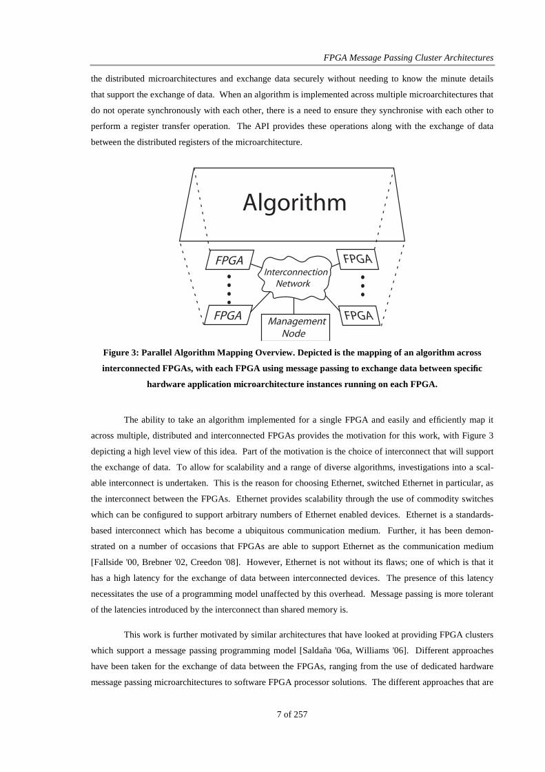
InterconnectionNetwork
FPGA ManagementNode
FPGA FPGA
FPGA
Algorithm
Figure 3: Parallel Algorithm Mapping Overview. Depicted is the mapping of an algorithm across
interconnected FPGAs, with each FPGA using message passing to exchange data between specific
hardware application microarchitecture instances running on each FPGA.
The ability to take an algorithm implemented for a single FPGA and easily and efficiently map it
across multiple, distributed and interconnected FPGAs provides the motivation for this work, with Figure 3
depicting a high level view of this idea. Part of the motivation is the choice of interconnect that will support
the exchange of data. To allow for scalability and a range of diverse algorithms, investigations into a scal-
able interconnect is undertaken. This is the reason for choosing Ethernet, switched Ethernet in particular, as
the interconnect between the FPGAs. Ethernet provides scalability through the use of commodity switches
which can be configured to support arbitrary numbers of Ethernet enabled devices. Ethernet is a standards-
based interconnect which has become a ubiquitous communication medium. Further, it has been demon-
strated on a number of occasions that FPGAs are able to support Ethernet as the communication medium
[Fallside '00, Brebner '02, Creedon '08]. However, Ethernet is not without its flaws; one of which is that it
has a high latency for the exchange of data between interconnected devices. The presence of this latency
necessitates the use of a programming model unaffected by this overhead. Message passing is more tolerant
of the latencies introduced by the interconnect than shared memory is.
This work is further motivated by similar architectures that have looked at providing FPGA clusters
which support a message passing programming model [Saldaña '06a, Williams '06]. Different approaches
have been taken for the exchange of data between the FPGAs, ranging from the use of dedicated hardware
message passing microarchitectures to software FPGA processor solutions. The different approaches that are

Introduction
8 of 257
taken is the motivation in this work for the development and comparison of the hardware microarchitecture
and the software FPGA processor across a single interconnect solution so that a direct comparison can be
performed between each approach. By looking at both approaches, the suitability of switched Ethernet as the
interconnection medium for supporting remote register transfer operations between distributed microarchitec-
tures can be measured and results compared with other FPGA cluster solutions. To help measure the suitabil-
ity of switched Ethernet, a number of criteria are investigated including:
• The reconfigurable overheads required for each message passing architecture
• The architecture’s ability to use the parallel hardware of an FPGA to its fullest
• The remote register transfer overheads measured in latency and bandwidth.
When combined, the motivation of this work is to look at providing an easy to use parallel pro-
gramming model which an application developer can use to perform remote register transfers between dis-
tributed microarchitectures running on multiple interconnected FPGAs. The use of switched Ethernet as the
only interconnect between the FPGAs is novel and has not been done in this manner before even though
switched Ethernet is the predominant interconnect used by cluster computing [SC '09]. Using a single com-
modity interconnect also allows for directly interfacing FPGA application microarchitectures and networked
computers, enabling them to exchange data with each other. This allows the FPGAs to be treated as peers on
the network rather than the more classical view of FPGAs as computation co-processors. Within this work,
investigations into the use of FPGAs as complete peers on the network is limited as the focus is on providing
a message passing programmers’ interface which can be used to exchange register data between distributed
application microarchitectures.
1.1.2 Research Structure
The research for this thesis has been undertaken to further develop existing processes for the parallelisation
of algorithms across interconnected FPGAs through the provision of an easy to use and programmer oriented
hardware interface which abstracts the application from the physical interconnect and communication opera-
tions. For this, there are a number of distinct sections to the research:
1. The first sees the development of the abstract application interface which will support the exchange
of data between the distributed application microarchitectures. This interface required the develop-
ment of an appropriate Hardware Description Language Message Passing Application Programming
Interface (HDL MP API). This interface supports the abstraction of the application from the meth-
ods used to exchange data between distributed hardware application microarchitectures.
2. The second examines an appropriate interconnection strategy for distributed FPGAs, with two dis-
tinct elements of research detailed. The first is the development of the message passing data ex-
change strategy that is directly used and supported by the HDL MP API. The second is the devel-
opment of the communication strategy that is used on the physical interconnect which supports the
exchange of data. In researching the message passing and communication strategy a hardware only
FPGA Message Passing Cluster Architectures
9 of 257
microarchitecture solution and a software FPGA processor solution have been developed and tested
on interconnects of varying capacity with a view to identifying the optimal solution.
3. The third section involves comparative testing of both interconnection solutions for the processing
of a variety of algorithms with a view to identifying characteristics of each approach that lend them-
selves to particular algorithm types.
4. Finally, as part of the development of the communication strategies, a new and novel algorithm for
the exchange of small amounts of data has been developed. The applicability of this algorithm for a
range of communication architectures is also undertaken.
1.1.3 Peer reviewed publications
Eoin Creedon, Michael Manzke, “Impact of Fragmentation Strategy on Ethernet Performance”, in Proceed-
ings of the 6th IFIP/IEEE International Conference on Network and Parallel Computing (NPC ‘09), 2009
[Creedon '09a]
Muiris Woulfe, Eoin Creedon, Ross Brennan, Michael Doyle, Michael Manzke, “Programming Models for
Reconfigurable Application Accelerators”, in Proceedings of the 1st Workshop on Programming Models for
Emerging Architectures held in conjunction with the 18th International Conference on Parallel and Compila-
tion Techniques (PACT ’09), 2009 [Woulfe '09]
Eoin Creedon, Michael Manzke, “Software vs. Hardware Message Passing Implementations on FPGA clus-
ters”, in Proceedings of Parallel Computing with FPGAs, held in conjunction with the 13th International Con-
ference on Parallel Computing (ParaCo2009), 2009 [Creedon '09b]
Eoin Creedon, Michael Manzke, “Scalable High Performance Computing on FPGA Clusters Using Mes-
sage Passing”, in Proceedings of the 18th IEEE International Conference on Field Programmable Logic and
Applications (FPL), 2008 [Creedon '08]
Eoin Creedon, Ross Brennan, Michael Manzke, “Towards a Scalable Field Programmable Gate Array
Cluster for Interactive Parallel Ray-Tracing”, in Proceedings of Eurographics Ireland Workshop, 2006
[Creedon '06]
1.1.4 Contribution
In this thesis, a parallel programming model facilitating algorithm parallelisation using interconnected hard-
ware microarchitectures implemented on multiple distributed and interconnected FPGAs, is developed. This
thesis uses message passing as the parallel programming model to support remote register transfer operations
between distributed FPGA application microarchitectures across switched Ethernet. The exchange of data
between the application microarchitectures allows an algorithm to be further parallelised across multiple
Introduction
10 of 257
FPGAs while through the use of an API supports remote register transfer operations between the microarchi-
tectures. To reduce the complexity of interfacing application microarchitectures with the message passing
remote register transfer operations, a hardware description language interface has been developed. This al-
lows the hardware microarchitecture to request and perform remote register transfer operations without re-
quiring knowledge of how the transfer will ultimately be performed, knowing only that the transfer will be
performed securely and reliably. The use of switched Ethernet, message passing and distributed FPGAs in
this manner has not previously been performed and along with the design and implementation of the message
passing application interface forms the main contribution of this thesis.
Through the use of the message passing programming model and distributed, interconnected
FPGAs, the contribution of this work sees the use of a hardware application interface which can be used by
distributed application microarchitectures to exchange data between remote registers and memory elements.
This ensures an algorithm can be parallelised and operated across the available resources of multiple inter-
connected FPGAs. Further to supporting the parallelisation of an algorithm across multiple interconnected
FPGAs, additional contributions of this work include evaluations of the performance overheads of both a
hardware message passing microarchitecture and a software FPGA processor microarchitecture. The contri-
bution from each of these relates both to how they perform in exchanging data between distributed applica-
tion microarchitectures and to how they implement the operations to exchange the data. Through the use of
the common application interface, it has been possible to evaluate both implementations using the same
hardware microarchitectures, further highlighting the benefit and contribution of using a hardware interface
between the application microarchitecture and the message passing exchange mechanisms.
When exchanging data across Ethernet, a means must be provided to split large messages into
smaller network-specific data fragments. The unique nature of the implementation platform allowed for
evaluations of different approaches to support this data fragmentation operation and ultimately resulted in a
novel approach. This contribution formed the basis for a publication [Creedon '09a] and showed that by re-
evaluating some of the more common approaches in network communication, performance advantages can
be achieved at minimal application implementation cost. The use of this updated fragmentation algorithm is
an additional contribution while the ability of the API to shield an application from low level network opera-
tions was further tested during these experiments.
1.2 Thesis Structure and Layout
This thesis is organised as follows: Chapter 2 looks at background and related works that have been used to
refine and motivate the research of this thesis. In particular, this chapter looks at parallel algorithms and their
operational requirements, at FPGA cluster solutions, the programming model they use, and how they are in-
terconnected. The architectural organisation and operational details are presented alongside shortcomings in
the various solutions. It is these shortcomings that this work addresses, presenting different solutions to the
overall research area.
FPGA Message Passing Cluster Architectures
11 of 257
From the information presented in Chapter 2, Chapter 3 details the design requirements that need to
be addressed when implementing a message passing, switched Ethernet FPGA cluster. These details are pre-
sented in an implementation-independent manner providing a high-level overview. This design has been
implemented, and Chapter 4 presents the implementation details. Certain features are common between the
hardware and the software solutions. These are detailed along with any updates that have been applied to
them, mainly an Ethernet controller update from 10/100Mb to Gigabit operations. Individual implementation
details of the hardware and the software solutions are presented, highlighting how they are configured.
Using the design and implementation from Chapter 3 and Chapter 4, experiments have been per-
formed to test the research question. As part of these tests and experiments, a number of publications have
been generated [Creedon '08, Creedon '09a, Creedon '09b] and all results are presented in Chapter 5. The
experiments include benchmarks of the two architectures, allowing for a direct comparison of each approach
and also against their ability to support distributed hardware application microarchitectures, the message
passing parallel programming model and switched Ethernet. These experiments concentrate mainly on point-
to-point operations although some collective operations requiring more than two nodes are performed and the
results evaluated. While performing the high level design, a novel approach to data communication was de-
vised for performing data fragmentation. Detailed experiments looking at the fragmentation approach on a
number of system architectures are evaluated and the results for these presented. The different systems in-
clude standard PCs using a custom communication protocol based on that used between the FPGAs and also
an approach using Transmission Control Protocol/Internet Protocol (TCP/IP) communication. Finally, ex-
periments evaluating the performance of the HDL MP API interface are undertaken using an algorithm de-
manding high performance, matrix multiplication.
Chapter 6 presents the conclusions to the thesis and provides the answer to the research question.
As the implemented platform was developed to address the research question, a number of limitations exist
and these are detailed along with future research and work that could be performed to address these.


13 of 257
Chapter 2
Background and Related Work
The research question as presented in Chapter 1 has evolved from a large number of different projects that
have looked at various aspects related to this research but not focused specifically on using switched Ethernet
in conjunction with message passing as the means to support distributed hardware application microarchitec-
tures across interconnected FPGAs. These related fields include parallel computation, FPGA application
acceleration, network communication acceleration and application parallelisation across multiple intercon-
nected FPGAs. This chapter investigates these areas of research to provide the motivation and developmen-
tal approach for interconnected FPGAs.
The first area of relevance is parallel algorithms and the requirements these place on both a compute
node and communication mechanisms. To help understand the general requirements of these applications,
software PC based approaches are detailed before discussing approaches and implementations that are practi-
cal for exchanging data between distributed application logic. PC based solutions are presented initially as
these represent the most mature environment which supports the operations that will be required for distrib-
uted FPGA hardware application microarchitectures. Parallel programming models are also discussed to
show how data can be exchanged by the application. As part of the details on parallel programming models,
different interconnect solutions are discussed as they pertain to why switched Ethernet would be used and
also what other approaches may be practical. These details aid in understanding the general field that is be-
ing researched in this thesis and gives an overview of the requirements that a distributed hardware application
will expect of a message passing, switched Ethernet solution.
The use of FPGAs as a computation acceleration platform is presented to show why the use of
FPGAs advantages parallel computations but also highlights concerns that arise in present approaches for
using FPGAs to accelerate these computations. This knowledge is of use as it refined the work so that direct
movement of data between distributed hardware application microarchitectures is employed as opposed to
other possible approaches where date is moved through a host system before being moved to the FPGA. As
part of the investigations into the FPGA acceleration logic, the approaches that can be used for exchanging
Background and Related Work
14 of 257
data between distributed hardware application logic is also detailed. FPGAs have demonstrated different
approaches for supporting network communications and these approaches along with configurations that are
relevant refine the approach that can be taken as part of the system design and experimental implementation.
Finally, details on other comparable solutions are presented to help put the work of this thesis into
context with what others are researching. This helps show the originality and contribution of this work while
also detailing comparable solutions which allows the research question to be addressed, is the use of switched
Ethernet as the interconnect between distributed FPGA hardware application microarchitectures a good or
bad approach to take.
2.1 Parallel Algorithms
Parallel algorithms detail the computations and communications that are performed across multiple compute
units in solving an algorithm. Fork-Join is one approach used to perform parallel algorithms where a single
processing unit performs all sequential operations before forking the data and operations across multiple
compute units to perform the calculations in parallel [Smith '03, Patel '06]. Once the parallel calculations are
completed, the results are joined back into a single compute unit which continues the sequential operations
before performing any future fork-join parallelisation operations. Fork-join describes the control approach
that is used by the parallel implementation of an algorithm but does not describe how data is moved between
the sequential and parallel aspects of the algorithms. The data exchange operations that are used depend on
the architectural approach and structures that the algorithm is being implemented on, with either a message
passing or shared memory approach applicable for the parallel algorithm implementation. In the operation of
a fork-join algorithm, data exchange occurs in three separate instances.
1. The movement of data between the sequential aspect of the algorithm and the parallel compute
units.
2. The movement of data between the parallel computation units where data can be exchanged between
the compute units depending on the algorithm requirements.
3. Data communications between the parallel compute units and the sequential aspect of the algorithm
as part of the join operation.
To help identify the operations that are typical in parallel algorithms, the Numerical Aerodynamic
Simulation (NAS) Parallel Benchmark [Bailey '94] is investigated. The NAS Parallel Benchmarks (NPB) are
a suite of benchmarks which classify the performance of a parallel compute system based on the achieved
performance across a range of computation types. These types are derived from the computations required in
Computational Fluid Dynamic (CFD) applications with eight computation types classified, Embarrassingly
Parallel (EP), Multigrid (MG), Conjugate Gradient (CG), 3D Fast Fourier Transform Partial Differential
Equations (FT), Integer Sort (IS), Lower/Upper Solver (LU), Pentadiagonal Solver (SP) and Block Tridiago-
nal Solver (BT). Each application type has been developed to test different aspects of a parallel architecture
from the individual nodes themselves to the interconnects performance to the overall system performance.
EP, MG, CG, FT and IS are the main kernel benchmarks used in evaluating a systems performance while LU,

FPGA Message Passing Cluster Architectures
15 of 257
SP and BT look to measure specific features of parallel architectures e.g. parallel I/O performance and how it
affects the computation of the system.
To help identify the parallel computation requirements, the five kernel benchmarks have been inves-
tigated further. The operations and implementation of these benchmarks for PC based solutions are detailed
first to show what computations are performed before both single and multiple FPGA solutions are presented,
showing how they operate on and across FPGAs. EP algorithms test the performance of the individual
nodes, by performing a large amount of computations against very few, although possible large, communica-
tions. The structure of the communications between nodes will vary depending on the EP algorithm that is
being implemented with both point-to-point and two-dimensional approaches possible. Matrix multiplication
[Choi '94] is an example of an EP classified computation, with the operations highly parallel as very little
data dependence exists within the algorithm against the amount of computations that need to be performed.
MG algorithms perform computations on regular two- or three-dimensional data grids, with the data of inter-
est represented as discretised data points on a grid, with more points representing a better model of the sys-
tem under investigation. MG computations are based on how these data points interact with each other, with
an MG computation complete when no new updates are performed across the grid, representing a state of
equilibrium. The computations performed on the MG grid are based on how neighbouring data points inter-
act with each other with all points interacting concurrently in the same computation cycle. New computa-
tions are performed in an iterative manner until a state of equilibrium is reached. In a parallel implementa-
tion, the grid data is divided across the compute units, each getting a sub-grid of the overall data. Communi-
cations between compute units are known in advance and do not change during the algorithm operations,
making MG algorithms structured in their communication operations. This is seen as only grid edge data
needs to be exchanged between neighbouring nodes to ensure the correct data is present for the next compu-
tation iteration. MG interactions mean boundary data is exchanged between computation units during each
iteration to perform all computations. Molecular Dynamics [Kalé '99] is classified as an MG computation,
where the interactions of atoms and molecules in a regular grid are measured. CG algorithms look to gener-
ate an approximate and accurate solution to linear equations which are typically composed of sparse matrix-
vector computations. CG algorithms use iterative approaches to reach a solution for the linear equation with
the solution being either the exact solution to the problem or an acceptably accurate solution. Each iteration
of CG algorithm refines the solution to being more accurate. Parallel implementations of CG are similar to
MG computations but the sparse matrix layout means data distribution is based on each node getting a part of
the matrix but a complete vector during each computation iteration [Bycul '02]. Data communications follow
a more master-worker model without many communications occurring between iterations. Lattice QCD
[Krieg '08] is a CG algorithm where simulations are used to measure the interactions and behaviour of sub-
atomic particles. Parallel implementations of CG based computations are not structured like MG computa-
tions with the communication operations more irregular. This is attributable to the sparse matrix setup of the
data and it not being known in advance what data interacts with which sparse matrix data on the compute
units. FT algorithms solve partial differential equations, allowing for the transformation of data from one
domain to another. Parallel implementations of FT algorithms see the exchange of data between compute
units across a range of communication paths, both to near compute units and distant compute units [Agarwal
Background and Related Work
16 of 257
'94], depending on the computation iteration. Two communication approaches are possible in a parallel im-
plementation. The first uses a data transpose operation before data segments are sent to different compute
units. The second sees the use of a butterfly exchange mechanism that sees successive iterations transfer data
between more distant compute units. IS computations sort a large integer space and test the integer computa-
tion operations of a compute node in conjunction with the communication performance as data is exchanged
continuously with associated nodes [Quinn '94]. LU, SP and BT applications test a larger range of opera-
tions than just the computations or the network, with the BT benchmarks having a higher degree of I/O based
operations to the other approaches. LU and SP algorithms are special sparse matrices which have data dis-
tributed across the diagonal and are used in numerical analysis and linear algebra.
Fork-join algorithms require support for interleaving both sequential and concurrent operations to
function correctly. Sequential operations require the use of a single, central compute unit which manages and
maintains knowledge about the overall results of the computations while concurrent operations see the direct
exchange of data between compute units. Support for this style of operation will be required to ensure cor-
rect and efficient support of parallel computation across the distributed FPGA hardware application microar-
chitectures. The NPB highlight features that are expected of parallel algorithms including the ability to sup-
port different data sizes for computations and communications along with the ability to support a range of
different communication topologies. These features will need to be integrated into the FPGA implementation
as part of the API so that a range of applications will be supported and not just a limited set. As part of the
API, no distinction should be made between compute unit types as the need to exchange data with either a
sequential or concurrent compute unit will be needed. To help answer the research question, measuring these
operations will help say if switched Ethernet FPGA clusters are able to meet the demands of parallel compu-
tation in a realistic and suitable manner.
2.1.1 Parallel Algorithm Communication Patterns
The parallel algorithm implementations in the NPB exchange data with other compute units to perform all
algorithm operations. The pattern of these communications are either structured, where the order of the
communications is known in advance and does not change during the algorithm execution or is unstructured
where for a given iteration in the algorithm it is not known which node has communicated with which node.
To help understand the style of communications that will need to be supported, an investigation into
those of the NPB benchmarks will aid develop these operations. Riesen [Riesen '06, Riesen '09] has under-
taken a detailed investigation into the NPB communication patterns, looking at which nodes are communi-
cated with frequently and the size of data that is exchanged between compute units. This work shows that the
range of compute units that exchange data is dependent on the number of compute units that the algorithm is
parallelised across. A range of data exchange topologies also needs to be supported, rather than specific, pre-
defined node-node communication patterns. This requires the need to support a dynamic communication
approach with the source and destination of each communication configured for the specific iteration of the
algorithm. Faraj and Yuan [Faraj '02] have investigated the communication patterns of the NPB, in particular
FPGA Message Passing Cluster Architectures
17 of 257
for the message passing implementations of the benchmark algorithms. They look at the communications
that are performed in an algorithm to see if code optimisations can be applied to improve communication
operations. They divide the communications based on dynamic or static and point-to-point or collective
communication operations as defined at application compile time. Point-to-point communications account
for the vast majority of operations while although collective communications are used by algorithms, they do
not account for a large portion of the data or a large number of operations. The average amount of data in
communications across all algorithms is approximately 43.6 KB with a range between 1.8KB and 191KB.
This information and that of Riesen show that during the execution of an algorithm, it is not possible to know
at all times and for all sizes which computation units are exchanging data, necessitating the need for support
of a dynamic communication pattern and range of exchange sizes which scales as the number of nodes scales.
Vetter and Mueller [Vetter '03] detail the communication requirements for a number of non-NAS
Message Passing Interface (MPI) scientific applications and similarly show a large number of point-to-point
communications. Vetter and Mueller present a more detailed breakdown of the communication sizes than
Faraj and Yuan and show a point-to-point packet size range between 90 bytes and 533 KB against an overall
average of approximately 1.5 KB. The collective communications that are performed only exchange small
amounts of data on the order of bytes, not kilobytes. The work of both Faraj and Yuan [Faraj '02] and Vetter
and Mueller [Vetter '03] show that a wide range of communication sizes are required by a range of parallel
applications. Further to the communication operations and sizes, communication patterns also play a role in
how data is exchanged between nodes. As well as the interface supporting variable sized communications,
the communication pattern as detailed by Faraj and Yuan [Faraj '02] is predominantly dynamic and unstruc-
tured in nature meaning the communication pattern is not known at algorithm compile time but rather based
on operations that will occur during algorithm execution.
From these observations on actual communication patterns of the NPB, the need to support efficient
point-to-point communications is paramount. Point-to-point make up the bulk of the communications that
will be expected between the distributed hardware application microarchitectures. Support for variable com-
munication sizes is also necessary with the sizes ranging from bytes to kilobytes and beyond. From the
communication patterns, collective communications should also be supported but on an algorithm by algo-
rithm basis. They are not always required but do provide necessary communication patterns which should be
provided to the distributed hardware application microarchitectures. This will require the development of a
parametric interface which allows for the inclusion of collective communications when required but other-
wise allows them not to be included. This should reduce the resource requirements for supporting the com-
munications while the development of a parametric interface should not require a new interface, more an
addition on the point-to-point communications that are used. The provision of a dynamic, parametric mes-
sage passing interface will address the research question as by supporting these features, a more realistic so-
lution can be generated which will demonstrate the feasibility of a switched Ethernet FPGA cluster.

Background and Related Work
18 of 257
2.2 Parallel Programming on Microcomputers
While details on fork-join and iterative approaches to solving parallel algorithms show what happens, how an
application can use these features needs to be discussed. The use of programming models aid the application
developer in expressing the computations and communications that are required while well designed and
developed parallel programming models should abstract the programmer from the underlying complexities of
how these are performed. This leads to the need for an easy to use, scalable parallel programming model
which supports the exchange of data between various, distributed compute units, matching up with the fea-
tures that have already been defined – dynamic communication patterns and sizes, variable numbers of com-
pute units, etc.. The exchange of this data ensures all computations for a given algorithm are performed cor-
rectly. The exchange of data between the distributed compute units can be supported in a number of ways,
either explicitly as part of a message exchange operation or implicitly where data is shared between multiple
units which can each access it [Werstein '03, SC '09]. Support for the exchange of data between units comes
in a number of manners but is typically supported through the use of an API which abstracts the implementa-
tion details from the programmer. This allows the programmer to focus on the computations and data distri-
bution operations to make the algorithm operate efficiently in parallel without needing to know how the
physical exchange of data will be performed. Both message passing and shared memory have different APIs
because of differences that exist in how data is exchanged between compute units and operations that need to
be supported. With the introduction of MPI [Forum '95], a single standardised API for message passing has
been possible while OpenMP [OpenMP '07] has started to become a standardised API for shared memory but
as yet no dominant API for shared memory exists.
The message passing paradigm uses defined messages for internode communication which are then
exchanged between the compute units. Message exchange functions are used by an application to generate
communications but apart from scheduling the communication to start, no control is in place as to when the
exchange will physically occur or complete. No memory space is shared in a message passing system, rather
all computation data is stored locally and encapsulated as messages when data is to be exchanged between
compute units. The message passing API allows an application assert message exchange functions between
interconnected compute units while also abstracting the programmer from the physical communication
mechanisms that are used. The programmer concentrates on the parallelisation of the algorithm without
needing to be concerned with how the message is generated and exchanged for a given platform [Forum '95].
In message passing systems, two types of message communications are defined, point-to-point and collective
communications. Point-to-point communications exchange data between individual compute units using
Send and Receive operations. Collective communications occur when a number of compute units are ex-
changing messages as one communication operation e.g. a broadcast where one compute unit sends data to
all connected compute units.
Shared memory creates a single large memory space which all nodes share access to. Access to the
shared memory is based on the address the data is located at. This makes all communication implicit in na-
ture as the location of the data may not be known in advance with it either in local or remote memory to the

FPGA Message Passing Cluster Architectures
19 of 257
compute unit accessing it. The location of data is dependent on how it is initially laid out in memory, with
some approaches yielding better results as data is stored locally compared with others where more communi-
cations can be necessary to access data. Where message passing is concerned with writing programs that
exchange messages across an interconnect, shared memory systems are concerned with accessing memory
which is shared between the compute units. The memory sharing operations can be achieved in a number of
ways, with the two most common being Uniform Memory Access (UMA) and Non-Uniform Memory Access
(NUMA). UMA creates a single large memory such that all accesses to memory, regardless of the node that
is performing the access has the same overhead. This approach makes the access time uniform and does not
suffer from concerns with how data is initially laid out across memory. NUMA on the other hand suffers
from non-uniform access times resulting in more efficient access to local memory than remote memory. As
part of a NUMA architecture, the memory which nodes access does not need to be local, allowing for
Distributed Shared Memory (DSM) environments where data is distributed across interconnected compute
units [Karl '99]. Unlike the message passing approach, all accesses in the shared memory approach are based
on memory operations, with the amount of data accessed on a per communication basis being less than that
exchanged in message passing. A shared memory API needs to support the sharing of memory between
compute units and also reading and writing operations that are possible to this memory. To ensure data sta-
bility and prevent corruption, memory locking operations are needed which enforce a single compute unit
accessing the data at a time.
This thesis is looking at message passing as opposed to shared memory for a variety of reasons in-
cluding the existence of a pre-defined API which supports the message passing programming model. As well
as the API – MPI – further reasons message passing is being researched include the fact that the API ab-
stracts the user from the physical communication implementation that is used allowing a hardware applica-
tion microarchitecture to exchange data locally with different compute units on the same FPGA or across an
interconnect to distributed compute units. This thesis is only concerned with using message passing to ex-
change data between distributed hardware application microarchitectures however, the use of message pass-
ing to exchange data between different compute units on the same FPGA has been demonstrated by others,
[Saldaña '06a, Williams '06, Ziavras '07], and details on their work is discussed in Sections 2.6 and 2.7. In
developing the message passing communication interface, a hardware API will need to be developed and the
features that this API requires have been detailed in Section 2.1 with more specific operations detailed in this
section. As no specific hardware message passing API exists, these interface operations need to be known so
that a robust and useful interface is developed.
2.2.1 Message Passing
The development and implementation of message passing clusters has followed the evolving nature of the
compute clusters on which it is implemented. Early message passing implementations were developed to
leverage unique features of the hardware that they were operating across e.g. Intel NX/2 [Pierce '88], PAR-
MACs [Hempel '91], Meiko CS-2 and others. The use of specific features of the hardware gave rise to in-
Background and Related Work
20 of 257
compatibilities between the codes of the different systems, making portability difficult. This posed a problem
as the message passing operations on the different systems were very similar in how the algorithm was paral-
lelised and implemented [Gropp '93]. To address this, a number of approaches were developed which looked
to hide the differences of the physical implementations of the systems. One of the early investigations into
this was the development of Parallel Virtual Machine (PVM) [Sunderam '90, Geist '94] which developed a
complete control and operation environment to support the exchange of data between compute units. This
still required the different systems to support the PVM model for correct operation. To address code port-
ability concerns between different message passing systems, the MPI working group was setup [Dongarra
'93] which created and standardised MPI [Forum '95] as a portable message passing API. MPI portability
stems from its adoption by all major vendors as the message passing parallel programming model while the
development of MPICH [Gropp '96] as a compliant MPI solution further aided adoption. MPI defines the
API that is used to exchange messages between co-operating compute units. It does not specify explicit im-
plementation approaches, leaving that to individual implementations. Support for MPI styled communica-
tions will aid the hardware API as MPI communication patterns should be transferable to the hardware API
without requiring much if any modifications.
When the specification of MPI was being developed, the MPICH system was created to test and
check the various MPI operations that were being proposed in order to define problems and concerns that
could arise [Gropp '96]. As MPICH was the first implementation of MPI and to ensure it could be easily
adopted for use on different compute clusters, a layered approach to its implementation was taken. This en-
abled support for different interconnects without needing to modify higher layers of the message passing op-
erations that are supported. To support this, all platform-dependent operations are encapsulated by the
Abstract Device Interface (ADI) [Gropp '94]. The use of the ADI allowed for the quick development and
porting of MPICH to a wide range of compute clusters while not preventing more tuned versions which inter-
face at different layers in MPICH to improve performance. Since MPICH, a wide range of MPI compliant
systems have been developed and implemented including Local Area Multicomputer (LAM)/MPI [LAM
'09], OpenMPI [Gabriel '04], MVAPICH [University '09], Fault-tolerant Embedded MPI (FEMPI)
[Subramaniyan '06], Embedded MPI (eMPI) [McMahon '96], Lightweight MPI (LMPI) [Agbaria '06],
Toronto Molecular Dynamics-MPI (TMD-MPI) [Saldaña '06a] and others. Most development has been for
microprocessor-based solutions which use a standard processor for the communication operations although
some specialised implementations do exist for dedicated environments e.g. eMPI [McMahon '96], TMD-MPI
[Saldaña '06a].
MVAPICH [University '09], LAM/MPI [LAM '09], OpenMPI [Gabriel '04] are microprocessor MPI
implementations which further extend MPICH functionality, either through augmenting and updating
MPICH or by using a new implementation taking on board the knowledge learnt from MPICH and large
scale scientific computations on clusters. MVAPICH [University '09] updates MPICH with an emphasis on
using hardware acceleration features present on Infiniband and Internet Wide Area RDMA Protocol
(iWARP) capable networks. Among the additional features are support for Remote Direct Memory Access
(RDMA) based operations and communication protocol stack offloading to dedicated communication hard-

FPGA Message Passing Cluster Architectures
21 of 257
ware. LAM/MPI [LAM '09] is a new implementation of MPI which does not use MPICH code. This results
in a different implementation philosophy with LAM/MPI looking to leverage the performance of cluster
computers more natively than MPICH. This is achieved by using daemons running on the compute units to
create the MPI communication environments. LAM/MPI also implements Interoperable MPI [IMPI '00]
which allows different implementations of MPI to communicate correctly with each other through the use of
bridging devices which translate between the different MPI implementations. Like MVAPICH before it,
LAM/MPI supports acceleration logic present on Infiniband, Myrinet and other high performance networks.
OpenMPI [Gabriel '04] is a new and updated version of LAM/MPI merging efforts from Los Alamos (LA)-
MPI [Aulwes '04, LA-MPI '09] and Fault Tolerant-MPI [Fagg '00, FT-MPI '09] to create a more robust and
fault tolerant MPI implementation meant for 10’s of thousands of nodes. The addition of fault-tolerance with
MPI code is driven by the scale of modern MPI clusters, into the 10’s of thousands, where the number of
compute units increases the likelihood of a failure. For scientific computations, a compute unit failure if not
handled correctly would prevent the application from completing properly. OpenMPI addresses this by using
a modular implementation approach which allows it to load the components on a case by case basis, reducing
the memory footprint and the MPI implementation complexity.
Further to the approaches detailed above, a number of embedded processor approaches have been
developed. eMPI [McMahon '96] looks at extending MPICH into the embedded processor domain. eMPI
takes two approaches for implementing MPI as part of an embedded processor cluster, the first looking at
removing unnecessary or costly aspects of MPICH for embedded processors e.g. memory requirements. The
second is a ground up, custom implementation which is built for the resources of the embedded processor
specifically. Comparisons on the two approaches show that although the custom solution outperforms the
MPICH implementation both in performance and memory footprint, the overall time to implement it can
outweigh the possible performance advantage. A further concern raised by the custom solution of eMPI is
that while it operates correctly, it is not portable across embedded processors as each processor has distinct
features and operations which will not be present on all devices. FEMPI [Subramaniyan '06] and LMPI
[Agbaria '06] are two other MPI implementations for the embedded domain. FEMPI [Subramaniyan '06] is
concerned with the implementation of a fault tolerant MPI system for embedded processors. They present
architectural considerations for embedded systems that need fault tolerance with the main concern being the
amount of resources the system can spare to perform both the fault tolerant operations and maintain efficient
computations. LMPI [Agbaria '06] is concerned with a lightweight MPI implementation for distributed em-
bedded devices. To achieve this, a subset of MPI is run on embedded processors while a microprocessor
server runs a complete MPICH version to exchange data with other MPI enabled systems and performs trans-
lations to LMPI as required. All LMPI communications between embedded devices are based on exchanging
data with the server node with no direct communications supported between devices.
All processor-based MPI solutions use software coded state machines and message queues to store
state information about both on going or future communications that have been requested but not yet com-
pleted. The operations in the above MPI solutions can be split into two main layers, the message passing
layer and the communication layer. The message passing layer handles all operations for message exchange

Background and Related Work
22 of 257
and synchronisation operations of the compute units. The communication layer performs the actual commu-
nication operations for exchanging the data between the compute units on the interconnect. The operations
are split in this manner as exemplified by the ADI interface of MPICH [Gropp '94] to ensure different, more
agile communication approaches can be used as either hardware or network performance allows. The devel-
opment of network offload architectures where communication operations can be performed at the network
interface has seen the modification of message passing implementations, aided by the layered approach, to
take advantage of these architectures [Dalessandro '05b]. The use of updated network and communication
operations is exemplified by the introduction and use of network communication offload logic where opera-
tions are performed on the network card or by separate, dedicated communication processors [Adiga '02].
The development of communication offload logic is driven by issues and performance concerns that are pre-
sent in cluster computing using standard communication protocols. This sections discussion on various MPI
implementations has been used in formulating an approach for the design, development and implementation
of the message passing architecture for this thesis. The two approaches that are detailed are either a layered
approach that communicates directly with other message passing systems (MPICH, MVAPICH) or a daemon
based approach where additional resources are set aside on a device to support the message exchange opera-
tions (LAM/MPI, OpenMPI). As the resources of an FPGA will be limited and to better support the use of a
message passing hardware microarchitecture, a layered approach is being used with the message passing op-
erations built on top of the communication operations. From the need to support both point-to-point and col-
lective communications, the layered approach also better lends itself to this as the collective communications
can be layered on top of the point-to-point communications. From the approaches of MVAPICH, LAM/MPI
and others, the use of the FPGA to accelerate the communication operations will be investigated and details
on the types of operations that can be accelerated are discussed in Section 2.2.4. The use of a layered ap-
proach will also allow the FPGA implementation to best use the resources that are available to it for a given
operation rather than constricting its operations.
2.2.2 MPI
MPI has become the de facto standard for providing the message passing programming model to cluster
computing. As part of the development of a message passing FPGA architecture, it is important to under-
stand the various features that are present in MPI which have made it so widely adopted. Details on the vari-
ous operations that a complete MPI approach is meant to support will aid in the development of the range of
operations that a hardware API should provide. The limited resources of an FPGA make all operations of
MPI impractical to be supported, as was seen with eMPI [McMahon '96], but the ideas and operations that
are possible will help the development of the message passing solution so that it operates similar to what a
programmer is use to. Like eMPI, the ability to include different features on an algorithm by algorithm basis
will aid the resource usage by ensuring only necessary operations are included as required. All details pre-
sented here for the MPI operations are based on information presented by Snir et al [Snir '98], Gropp and
Lusk [Gropp '93] and detailed investigations into the implementation of MPICH [MPICH '07].

FPGA Message Passing Cluster Architectures
23 of 257
Point-to-Point Communications
Point-to-Point communications are used to directly exchange data between nodes on an individual basis, in-
dependently of the operations of other nodes. The main point-to-point communication methods are Send,
Receive, and Send_Receive. Send is used to send data from one node to another directly, with a node identi-
fied by a node identity integer which is unique on all nodes. An appropriate receive must be asserted at the
destination node to ensure the communication completes correctly. Send and receive operate independently
of each other and each must be called when required. Send_Receive is used to assert both the sending and
receiving logic concurrently. Associated with the point-to-point communications, are communication modes
and communication style. Three communication modes are defined for both sending and receiving. These
modes are synchronous, buffered, and ready. Synchronous mode communications complete once matching
send and receive pairs are present for the exchange of data between the nodes. Buffered communications use
dedicated temporary storage at the sending node to store the message before it is sent to the receiving node.
The use of buffered communications allows a send to complete at the local node independently of the actual
communication. Ready communications are the opposite of buffered as far as a ready mode communication
starts sending the data to the receiving node and it is the responsibility of the receiving node to store and cor-
rectly operate on the incoming data. For the correct completion of a ready mode communication, the receiv-
ing operation must be posted before the send starts.
Two communication styles are defined in MPI, blocking and non-blocking. Blocking communica-
tions halt the execution of the application until the communication completes. In blocking communications,
the completion of a communication allows for the reuse of the communication buffer. Non-blocking com-
munications, on the other hand, complete once the necessary communication configuration operations have
completed. The return from a non-blocking communication does not mean the communication has actually
started and before buffers are reused, testing on the communication must be performed. Non-blocking com-
munications allow a node to generate multiple communications while not preventing the continued execution
of the application code. However, for non-blocking communications the associated communication buffers
can not be reused until the communication has completed. Dedicated Wait methods are provided which can
be used to test if one, all or any outstanding communication has completed. Waiting and testing of the com-
munications is a blocking operation so it should only be performed once all application computations for this
iteration are complete. If either blocking Send or Receive are used, only unidirectional communications are
possible while using either Send_Receive or non-blocking communications, bidirectional communications
can be performed.
Collective Communications
Collective communications perform a single communication operation across all nodes of a single communi-
cation domain. Collective communications are implemented on top of the point-to-point communications
and are optimised to perform the specific communication based on the number of nodes or the message size
that is being used. This makes them efficient in the operations that are being performed as opposed to indi-

Background and Related Work
24 of 257
vidual point-to-point communications being used. A range of different collective communications are pre-
sent, but the main idea of them is that one or mode nodes have data that all nodes need to receive and proc-
ess. Two types of collective communications are supported, static and vector defined communications.
Static collective communications exchange the same amount of data between nodes in the given communica-
tion domain. Vector collective communications exchange a pre-set amount of data between specific nodes,
with the size of the exchanged data possibly different from one node to the next.
Communication Controls
As part of both point-to-point and collective communications, the idea of testing and cancelling of out-
standing communications arises. The use of communication controls allows for the better control and opera-
tion of an MPI based test and provides a degree of stability if a node should fail. Communication controls,
allow for the notion of speculative communications which can then be cancelled when they are not going to
complete. A direct example of a communication control is the wait and test operations.
Data Alignment and Data Types
The design criteria of MPI is that it should operate independently of the physical nodes and endians of the
implementation systems. To allow for this, a wide variety of data conversion routines are provided which
convert the data from one configuration to another. The use of these data conversion methods is possible at
the application though, investigations within MPICH show that to allow the system to operate across hetero-
geneous systems, data conversion methods are extensively used.
Standard C programming languages allow for ‘struct’ configurations on the data whereby a single
type encapsulates a variety of base types. This functionality has been provided as part of MPI through the
various data type and data alignment methods. The ability to control data at this level ensures a better match
is present between the various systems, independently of the physical implementation.
Communicator Domains
A communication domain is the collection of compute nodes into an abstraction notion consisting only of
those nodes. One single global communication domain is present and this maintains knowledge of all nodes
present in the compute cluster. Each node in a communication domain has an abstract node identity that
identifies it within that domain. The node identity within the domain may be distinct and different to the
global node identity for that node within the global communication domain.
The use of multiple communication domains allows a programmer to split the operations and control
of an application into distinct units with each domain performing a specific application operation. Each do-
main is viewed as a unique entity, independent of the overall global communication domain. To allow for
the exchange of data between communication domains, a single node within the domain is configured that
can talk to and communicate with an equivalent node within a different domain.
FPGA Message Passing Cluster Architectures
25 of 257
Topology Control
MPI assumes no particular ordering or operational configuration for the cluster nodes that are used. It finds
and initialises all requested nodes to perform a given computation. For certain computations, a particular
logical ordering will allow for better control and fit to the available interconnects of the compute cluster. To
address this need, MPI provides topology operations. Topology controls allow the programmer to logically
re-order the cluster nodes so that a better match for either the physical nodes or the application communica-
tion requirements is made. This can be used for two dimensional computation operations where the nodes
are organised into easily identifiable nodes on a grid. This makes the exchange of data around the nodes
more programmer oriented. Further topology operations are possible for graph based systems however, in-
vestigations into graph topology operations has not been undertaken.
The details on message passing and MPI, show the style of operations that are expected of the pro-
gramming model that is being used. From the details on MPI, the following concerns are present and must
be addressed as part of the evaluation of the system including the performance of the point-to-point and col-
lective communications that an application may use and which are present in MPI. By supporting these op-
erations, a more MPI oriented approach to the remote register transfer operations will be possible which will
reduce the overheads in learning and using the distributed hardware application microarchitectures. Not all
features of MPI however are practical for an FPGA with data alignment and data types a prime example as
all data operations of a hardware application will be specific to its implementation which will be common
across all the interconnected FPGAs.
2.2.3 Interconnects
While message passing and MPI describe the operations that need to be supported to exchange data between
distributed hardware application microarchitectures, cluster computing approaches use a scalable intercon-
nect to physically exchange the data. The choice of programming model has an influence on the interconnect
that can be chosen along with the approaches to the different communication operations that need to be sup-
ported. As message passing is being used as the programming model, only interconnects appropriate for
message passing are discussed. While these interconnects are appropriate for message passing, some are also
appropriate for use in shared memory configurations. Through the use of commodity interconnects, it is pos-
sible to create compute clusters consisting of large numbers of compute units [Sterling '95], into the 10’s and
100’s of thousands. Commodity interconnects which have been used for message passing compute clusters
include Infiniband [Association '08], Quadrics [Petrini '02], Myrinet [Boden '95], Scalable Coherent Interface
(SCI) [IEEE '92a], Silicon Graphics Inc.(SGI) NUMAlink [SGI '05a], 1/10Gb Ethernet [IEEE '05, Tuchler
'09]. The explicit communication and scheduling approach of message passing allows it to operate efficiently
on both high performance and lower performance interconnects [Liu '03a]. For best performance, the higher
performance interconnects increase the amount of data that can be communicated and reduce the time to ex-
change this data, however in a message passing cluster, the performance of the interconnect can also be con-
Background and Related Work
26 of 257
nected with the cost of implementing the cluster. The ability of message passing applications to more easily
tolerate lower performance interconnects allows cheaper clusters to be built which do not use the most ex-
pensive interconnects available. While it is possible to use any of the above interconnects to exchange data
between distributed FPGAs, this work is focused on using switched Ethernet. This decision is based partly
on the availability of the necessary networking resources and also because other solutions looking at inter-
connecting FPGAs are not investigating the use of switched Ethernet and are rather looking at point-to-point
interconnects. To help understand what approaches can be taken for interconnecting the FPGAs and as part
of overall cluster operations, the above interconnects are discussed in further detail.
Infiniband
Infiniband [Shanley '02, Association '08] is a high performance interconnect that supports both switched and
direct connection topologies. Infiniband provides low latency, high bandwidth communications between
nodes, with three speeds of operation specified - single data rate, double data rate and quad data rate – and
three modes of operation supported – x1, x4, x12. Infiniband is based on serial, bidirectional links, with the
base x1, single data rate configuration operating at 2.5 Gbps. Infiniband performs all communications be-
tween nodes based on 4KB ‘messages’, which when combined at the receiving node create the communi-
cated data. As part of the communication, Infiniband supports both reliable and unreliable approaches for
exchanging data. These operations are part of the underlying Infiniband implementation and are separate to
any high level reliable communication mechanisms that can be used. To support reliable and low latency
communications, network offload operations are performed at the interface including RDMA operations and
reliable communication operations. RDMA operations are supported to reduce the communication overheads
and host processor, network communication operations. To support RDMA operations the offload logic
needs to support address translation and direct memory access operations. As part of these operations, data
needs to be pinned in memory to ensure the address will be static and ensuring the correct data is accessed by
the network.
Quadrics QsNet
Quadrics QsNet [Petrini '02, Quadrics '07] is a High Performance Computing (HPC) interconnect that has
been designed and developed to deliver low-latency short message communications between connected
nodes. This is achieved through the use of hardware acceleration units and a communication processor oper-
ating at the network interface. The processor supports Direct Memory Access (DMA) operations to move
data across the network between interconnected devices. As part of the DMA operations, the entire address
space of both a compute node and the compute cluster can be accessed by the network controller. The com-
munication processor is used to perform communication protocol processing that is needed along with ad-
dress translation between network card, host computer and network accesses. This removes the host proces-
sor from performing these operations, freeing it to perform computations as opposed to network operations.

FPGA Message Passing Cluster Architectures
27 of 257
Myrinet
Myrinet [Boden '95] is a high-speed System Area Network (SAN) used for high performance, low latency
systems. To support this, Myrinet employs the LANai communication processor which performs all com-
munication operations. The LANai consists of a Reduced Instruction Set Computer (RISC) microprocessor
and additional packet interface and processing logic. To reduce the overheads for operating the Myrinet net-
work and interface, additional Static RAM (SRAM) memory is associated with the LANai, which can be
accessed through DMA operations both from the LANai and host computer. This is used by the host com-
puter as a storage space for data that is to be communicated across Myrinet. Myrinet uses low overhead
switching technology in connection with wormhole routing, allowing for low latency interconnection topolo-
gies while not limiting the topologies that can be used.
SCI
SCI [IEEE '92a] is a high throughput, low latency interconnected designed for distributed shared memory
clusters. SCI was developed from the FutureBus project [IEEE '92b] that also resulted in the creation of In-
finiband. SCI provides NUMA and DSM capabilities to standard compute cluster nodes by allowing local
memory to be shared between the interconnected compute nodes. To support this correctly, application data
must be pinned in memory and all accesses to remote memory are performed using DMA and RDMA opera-
tions. SCI uses a lightweight communication protocol which results in reduced latency. While SCI was de-
veloped for shared memory systems, it has been used as part of message passing systems [Herland '98, Karl
'99], with the necessary operations layered on top of the SCI communication functionality.
SGI NUMAlink
The SGI NUMAlink [SGI '05a] is SGIs' proprietary interconnect technology used to create large globally
shared memory clusters. These clusters implement cache coherent NUMA environments with NUMAlink a
low-latency interconnect which is able to access all memory on all connected compute units. To operate cor-
rectly, NUMAlink is connected into the systems memory interface, as opposed to being interfaced across a
peripheral I/O bus as occurs with the other interconnects that have been detailed. This tight interfacing of
NUMAlink with the system memory interface provides its low latency operations with transfers between
compute units typically small, processor cache line data transfers. Like SCI, message passing implementa-
tions have been built on top of the global shared memory infrastructure that is provided by the NUMAlink
[SGI '05b].
Ethernet
Ethernet [IEEE '05] unlike the other interconnects was not designed as a high performance interconnect
rather, it was developed to support the exchange of data between commodity computers. This is seen in the
range of speeds that Ethernet supports 10 Mbps to 10Gbps, with compatibility between the different versions

Background and Related Work
28 of 257
one of the key features of Ethernet. A typical Ethernet configuration sees it used in a switched star topology.
The compatibility between different versions and the use of a switched topology result in Ethernet being a
high latency interconnect as opposed to the others which have been discussed which are all low latency. As
the original configuration for Ethernet was not high performance networking, no network processing features
are present or required as part of the standard, rather Ethernet provides only basic functionality to exchange
data between connected devices. The limited functionality that is presented at the Ethernet network interface
makes it a cheaper approach for connecting compute units while the fact that it is a commodity interconnect
further reduces the expense in using it for high performance computing. The reduced cost is a reason that
Ethernet is the predominantly used interconnect of the fastest supercomputers [SC '09]. The limited support
for communication acceleration does however increase the overheads on performing data exchange and this
has seen active development in network acceleration for Ethernet networking [Bellows '02], with concepts
from other high performance networks used, including the addition of network communication processors to
the network interface [Shivam '01].
Different interconnects have been detailed to show other approaches that are possible for providing
the communication medium between the interconnected FPGAs. Customised approaches to supporting the
communications have not been presented as part of the interconnect operations, rather these are detailed as
part of the related work, Section 2.7, where more specific details on these approaches are given. While this
work is setting out to look at switched Ethernet, the structures and operations of other interconnects highlight
issues and concerns that arise for a range of approaches to support cluster and parallel computing. From the
more specialised high performance interconnects, it is apparent that support for the communication opera-
tions is required to improve the overall data exchange performance. As this is the case, details on possible
network acceleration operations that can be undertaken and why these have been developed both for Ethernet
and also for the high performance interconnects are now presented. It should be remembered that while the
program is defining the exchange of data as messages, it is the underlying interconnect and any communica-
tion protocols that will perform the actual data exchange. Any improvements in their operations will result in
more efficient message passing applications.
2.2.4 Network Operation Acceleration
Network acceleration operations have become common for HPC interconnect architectures as a means to
reduce the overheads in exchanging data between distributed compute units or to support specific architec-
tural requirements – DSM. Network operation acceleration stems from the fact that for all communications,
there is additional overhead associated with the data – the communication protocol – and processing of the
protocol has not kept pace with the increased network speeds or higher compute power that are available
[Markatos '02]. Part of the is caused by the frequency of packet arrival, with Bellows et al [Bellows '02]
showing that at maximum receival rate, computers were unable to process Gigabit traffic when it was first
introduced. Operating System overheads that a new packet arriving creates, including interrupts, context
switches and reduced processor availability, results in a lower than expected performance from the network
while also reducing the amount of computations that can be performed through lost computation cycles

FPGA Message Passing Cluster Architectures
29 of 257
[Tanenbaum '03]. The problem of reduced performance based on packet arrival rate presents itself for each
new generation of network that is introduced though over time, the processor advances enough to mitigate
against this. An issue for HPC is that the most efficient network is usually strived for while the computations
that an algorithm requires also advance – higher accuracy, larger dataset. This mismatch between the avail-
able and expected network performance is a cause for concern as the more time the processor needs to spend
handling network protocol processing, the less time it is able to spend on application computations
[Gilfeather '01, Fenech '04]. A number of projects have looked at improving the communications perform-
ance of the network by placing network accelerators at the network interface, and remove this processing
from the operating system and computer. This has led on numerous occasions to investigations into network
offload logic which removes the processor from the communication and uses dedicated communication logic
to perform these operations [Underwood '01b, Mogul '03, Currid '04] with most modern networks supporting
protocol offloading e.g. Infiniband [Association '08], Myrinet [Boden '95], Quadrics [Quadrics '07], 10 Giga-
bit Ethernet through the iWARP specification [Feng '05, Consortium '09]. While the use of network accel-
eration logic will aid the exchange of data between distributed FPGAs as part of this research and as the op-
erations are being developed on top of switched Ethernet, an investigation into different operations that have
been used and which may aid the overall structure and operation of the cluster are presented here. These de-
tails are presented for commodity computing solutions, with specific FPGA configurations presented in more
detail in Section 2.4.1 as part of an investigation into the use of FPGAs in networks.
Network accelerators look to increase the achievable network performance by executing network
operations on dedicated hardware while freeing the processor to perform algorithm computations and calcu-
lations. This leads to the idea of communication offload [Currid '04] where dedicated logic performs com-
munication operations. Communication offload operations have advanced both as the speed of networks
have progressed but also as the complexity of communication protocols have evolved. From early offload
operations dealing with interrupt coalescing [Mogul '97] to the offloading of complete network protocols to
the controller [Jaganathan '03, Mogul '03] to the operations of complete data movement and network stack
operations [Liu '03b, Dalessandro '05b, Dalessandro '06], the complexity of network controllers has in-
creased. While network offloading can improve network performance, a number of issues arise amongst
them the issue of mismatched processors to network offload logic, integration of the hardware into the proto-
col operations and portability across different architectures. When the network is able to saturate a processor,
offloading offers a distinct advantage and ensures the processor can perform computations however if the
processor is able to saturate the network, the offloading operations become a bottleneck reducing the achiev-
able performance [Shivam '03]. This means that although offloading does allow computers to operate
efficiently on newer networks the processor will eventually catch up and nullify the use of an offload com-
municator for that network. However by the time the processor is able to catch up, a newer faster network
speed has typically been developed and begun deployment [Pope '07]. The use of an offload communicator
aids overall performance operations as the processor is freed to performing computations against having to
perform both communication and computation operations that it would have to perform in the absence of an
accelerator [Bellows '02, Viet '05]. Interfacing the network accelerator with the processor and how the op-
erations are partitioned across the resources poses a concern. Freimuth et al [Freimuth '05] look at this issue

Background and Related Work
30 of 257
and identify the cost of moving data across the interface bus between the processor and the network as a per-
formance bottleneck. They recommend partitioning the interface operations so that the total number of bus
transfers between the processor and the network are reduced to a minimum.
Gilfeather and Underwood [Gilfeather '01] discuss the concerns of modern high speed computing
systems and the issues that network accelerators look to address. These include memory copying, frequent
interrupt generation and processor operation overheads. For memory copying, the fewer memory copies that
are performed on the data, the better the communication performance however once the computer memory
bandwidth is great enough, the cost of performing memory copies diminishes. The concern is when memory
and network bandwidths are similar in which case there is a large penalty for performing memory copying.
For network communications, it is rare that a packet will be received in isolation, rather a number will arrive
one after the other. Each packet that is received can result in the generation of an interrupt which the micro-
processor must handle. The rate of interrupt generation can cause problems for the microprocessor as they
are able to swamp it, preventing it performing further operations [Bellows '02]. Interrupt coalescing [Mogul
'97] is a common approach used to reduce the impact of interrupt generation. Interrupt coalescing reduces
the amount of interrupts that a microprocessor has to handle, rather a single interrupt is generated when a
new packet arrives while the microprocessor is not processing any packets. Once the microprocessor is proc-
essing network packets, it polls the network for new packets rather than waiting for interrupt generation.
This reduces the overhead on the processor and can result in higher packet processing operations. The con-
cern with this approach is that there is an increase in packet processing overhead resulting in a higher latency.
This arises as interrupts may not be generated immediately, rather a timeout or the presence of a certain
number of packets can be needed.
Although offloading does allow for improved network performance, the movement of data between
the processor and the offload logic can still be as complex as the protocol processing operations that were
needed to move the data between the processor and the network. Farrel and Ong [Farrell '00] show that the
software/hardware interaction slows down the performance of the network by reducing the available re-
sources for TCP/IP operations, while Shivam et al [Shivam '01] have identified a similar problem in that the
bottleneck for computation has moved from the network to the communication software. The interaction of
the offload logic and the network while not a direct aspect of the research question does pose a concern as to
the level of integration that needs to be supported and issues this will impose. For the message passing im-
plementation a layered approach will be taken but how will the network be implemented and where network
operations can be performed will cause issues with the architecture. Further, from the data movement over-
heads and protocol offload operations that are detailed, some motivation for this thesis can be developed,
namely if the overhead of moving data between the application and network can be removed does this impact
the applications operations or have any influence on the overall operations of the system. A range of differ-
ent operations related to network acceleration have been presented and show the style of operations that the
FPGA solution will need to implement and take into account. These operations include protocol processing,
data movement between the network and the application and network availability to ensure data can be ex-
changed between compute units without causing degraded performance. The use of FPGAs allows for con-

FPGA Message Passing Cluster Architectures
31 of 257
current computation and communication operations so this does remove some of the bottlenecks that network
acceleration logic look to address in computers but the underlying operations that are performed will need to
be addressed correctly.
Communication Offload Operations
The overhead issue has lead to the investigations of network processors and how these can be used by both
high performance computing networks and commodity networking to improve communication operations.
Network offload engines are used at the network interface to perform the communication operations that are
needed to exchange data between compute units. The communication processors of Myrinet and Quadrics
are network processors while the use of network processors in Ethernet networks is not unheard of [Shivam
'01]. As highlighted by Shivam et al [Shivam '03] offload engines offer a perform advantaged while the
amount of available network bandwidth is able to saturate the resources of a compute unit with O’Dell
[O'Dell '09] showing that for each advance in networking technology, the use of networking offload engines
for more operations reoccurs with more operations supported by the network offload logic. Investigations
into the use of network offload engines have looked at introducing dedicated microprocessors into the net-
work interface to perform either the complete network protocol stack or parts of it and thus free the computer
to perform calculations [Fiuczynski '98]. A number of approaches have been taken while investigating net-
work offload operations with a common theme being to perform as much operations in user space against
kernel space, in effect bypassing the Operating System (OS) and the associated overheads OS interactions
introduce [Shivam '01].
Ethernet Message Passing (EMP) [Shivam '01] looks to improve the performance of message pass-
ing through a combination of OS bypass operations and network offloading. As part of these operations, di-
rect memory accessing is supported from the network with data pinned in main memory before the commu-
nication occurs. Pinned memory is memory that is under the control of the user and the OS is not to page or
otherwise modify the address of the memory. The use of user level memory reduces the OS operating over-
heads. Arsenic [Pratt '01] has taken a similar approach and uses processors on the ACEnic to perform com-
munications between user memory space. Operating in user space presents challenges connected with multi-
ple data streams and the need to multiplex each stream. Arsenic addresses this on the network itself while no
details on this are presented for EMP. Communication partitioning between the microprocessor and the
Network Interface Controller (NIC) sees certain operations remaining in user space, mainly to do with higher
level communication protocols while the protocol processing operations are performed on the NIC itself.
Freimuth et al [Freimuth '05] note that the drop off in performance for faster networks is not a problem need-
ing faster processors, it is one which needs more efficient use of the interface busses between the NIC and the
processor. To achieve this Freimuth et al use a network processor to perform the protocol operations while at
the same time reducing the bus communication operations that need to be performed. Binkert et al [Binkert
'04] argue that network operations can no longer be an afterthought for system development and argue for
placing network control logic on the processor die, rather than on the network controller. To achieve this,
Binkert et al [Binkert '06] argues that First In, First Out (FIFO) buffers should be present on the processor die
Background and Related Work
32 of 257
and be directly controllable by the processor software. This mitigates the concerns posed by newer networks
or code modifications to support new accelerators as all operations are performed through software on FIFOs.
Real World Computing Partnership (RWCP) has investigated a custom communication environment
consisting of both switches and NICs, to provide a low latency, high bandwidth communication environment
for distributed computing [Kudoh '99]. Both Reconfigurable Logic [Izu '02, Tanabe '05] and Application
Specific Integrated Circuit (ASIC) [Watanabe '07] systems have been implemented, with network offloading
used to improve network communication operations. An RDMA based communication scheme is used for all
data communication operations. The International Business Machine (IBM) BlueGene system [Adiga '02] is
a massively parallel processing system consisting of up to 65,536 nodes. Each node consists of two
PowerPC embedded processors where one processor is used for computations while the second processor is
used primarily for communication. In this configuration, the second processor is used as a network offload
engine, focused mainly on network communication operations. Viet et al [Viet '05] while investigating ma-
trix multiplication on an Symmetric Multi-Processor (SMP) cluster look at the computational as well as
communication overheads that are incurred if one processor prioritises network operations over computa-
tions. They look to use both processors to perform computations but to maintain one processor for dedicated
communication operations. The premises is that communications will not always be on going while the addi-
tional processor can aid computation without impacting communication operations. They show that in this
configuration, a speed up is seen for both network and computation operations.
Communication offload engines do allow present day processors to achieve future networking per-
formance but they do pose a wide range of operational overheads. The first of these is the modifications that
need to be made to already existing communication protocol implementations to support the offload opera-
tions that are present [Shivam '03, Freimuth '05, Pope '07]. This can be seen in MPI with the specialised ver-
sions for Infiniband and other network solutions which employ communication offload operations. This is
further compounded by different offload operations from different systems meaning no one approach for
offloading operations has come to the fore. Recently, with the development of iWARP the use of a single
approach is becoming more realistic [Dalessandro '06], particularly with the development of software
iWARP implementations which allow for the exchange of data between iWARP enabled and non-enabled
systems [Dalessandro '05a, Joglekar '06]. At the highest level, the development of these accelerators is based
on the premise of delivering as much networking performance as is present to the application. By using ac-
celerators, each compute node is able to spend more time performing application computations while not
sacrificing the performance offered by cluster based systems.
Message passing algorithms are designed to use the message passing programming model, exchang-
ing message data and synchronising with each other as part of a fork-join approach to ensure they perform all
computations correctly. A major overhead in the message exchange operations are the communications that
need to be performed. To improve the performance of communications in general, network offloading is
employed with the performance advantage it provides applied extensively to high performance and cluster
computing solutions. This can be seen in the specialised MPI implementations (MVAPICH) and the ADI of
MPICH allowing for different network implementation solutions. The use of network offloading to improve

FPGA Message Passing Cluster Architectures
33 of 257
the network communication performance provides message passing applications with access to as much of
the available network bandwidth as possible between the interconnected compute units of the cluster. How-
ever, the use of offload logic still poses a problem as to how best access and use the available resources of the
network. In this thesis, network offload ideas are taken into account when developing the experimental
setup. From network operation acceleration and communication offloading, issues with the cost of perform-
ing communication operations on dedicated hardware need to be taken into account.
The use of specific logic does aid the performance of the network communications and protocol op-
erations with the advantage that both computations and communications can occur concurrently. To support
this efficiently, the interaction between the network operations and the compute unit need to be simple, robust
and easily used. Again, this aspect of the network operations provides a degree of motivation for this thesis,
by allowing for an investigation into the effect operating the network and the application logic on the same
hardware has. By using an FPGA, the application can be updated while the network and message passing
operations do not need to be changed. Through the use of a hardware API, these operations can be better
leveraged as many applications can be implemented to a single interface while a layered approach to the net-
work and message passing operations allows for a number of different approaches to supporting the data ex-
change mechanism independently of the application.
The details presented so far have focused on the mature area of microprocessor and network proces-
sor architectures and how algorithms and programming models have aided in parallelising computations
across many interconnected devices. These details help frame the area of research and the styles of ap-
proaches that are applicable for interconnected FPGAs both from the interconnects that are feasible and the
programming model along with what needs to be supported to allow for an easy to use and operational archi-
tecture for parallelising algorithms. With this information, details on FPGAs and how they have been used to
perform and accelerate a range of parallel algorithms are now presented. As part of the discussion on FPGA
application acceleration, details on various physical architectures which support application acceleration are
detailed. This includes features of the FPGAs themselves and also how FPGA development environments
can be implemented, with single or multiple FPGAs interconnected to provide the required resources. Simi-
lar to the discussion for microprocessor based solutions, the discussion then moves to how FPGAs have been
used to accelerate network communications, finally providing details on message passing FPGA solutions
and how they have integrated the different aspects of the architectures together to support application paral-
lelisation across interconnected computation units. To start the discussion, the use of FPGAs to accelerate
the NPB kernels are presented with the architecture of how this acceleration is achieved detailed.
2.3 FPGA Algorithms and Acceleration
FPGAs have been demonstrated on numerous occasions to accelerate the performance of a range of computa-
tions. This has been with the core computation logic of the algorithm implemented in a number of ways in-
cluding as dedicated microarchitectures [Callanan '06a], as illustrated in Figure 4, or as systolic array con-
figurations with multiple processing elements operating in parallel on a single FPGA [Zhuo '04], as shown in

Background and Related Work
34 of 257
Figure 5. To help develop the research question, the hardware API and the structures that are appropriate for
evaluating the research question, FPGA implementations and requirements of the NPB are discussed. By
looking at these algorithms, the functionality that a hardware API should provide to various microarchitec-
ture implementations can be developed, while also highlighting application characteristics that will need to
be supported. Using the order already present for the NPB, different FPGA implementations are discussed
with attention given to the features and structures that are required to implement the algorithm logic and to
accelerate the computation. These details are for single FPGAs with all computations performed on one
FPGA. Discussions on parallelising the algorithms across multiple FPGAs is performed in Section 2.4 after
the various architectures of multiple FPGAs has been presented.
COMPUTE
UNIT
COMPUTE
UNIT
COMPUTE
UNIT
Figure 4: Microarchitecture acceleration
structure, with data pushed into compute units
which pass the results onto other units for further
computation. Each compute unit can perform
different operations on the same or different data.
PROCESSING
ELEMENT 0
PROCESSING
ELEMENT 1
PROCESSING
ELEMENT N
Figure 5: Systolic Array acceleration structure,
with data exchanged between processing
elements in a known pattern. Each processing
element performs the same operations, except on
different blocks of a larger dataset.
2.3.1 NAS Parallel Benchmark FPGA implementation
EP algorithms perform a large amount of independent computations and are usually compute bound. Matrix
multiplication [Zhuo '04, Dou '05, Creedon '08, Kumar '09] and RayTracing [Schmittler '04] are EP computa-
tions that have been demonstrated on FPGAs. Usually EP problems are based on solving large datasets
which must be stored efficiently and usually requires the use of external memories interfaced with the FPGA.
To accelerate EP computations, multiple processing elements are connected in parallel on the same FPGA,
with common data shared between each processing element allowing all units operate in parallel. The use of
systolic array approaches to interconnecting the units and exchanging data between them has been employed
in matrix multiplication for both one-dimensional [Zhuo '04] and two-dimensional acceleration architectures
[Amira '02].
MG computations are based on how data points on a grid interact with each other. The computa-
tions of an MG calculation are completed when no new interactions occur because a state of equilibrium has
been reached with no new data point updates arising. Heat Equation [Fuentes '06] and Molecular Dynamics
[Gu '07] are MG computations which have been performed on FPGAs. To accelerate these on an FPGA,
multiple independent compute units are connected in parallel, with neighbour data points on the grid ex-
FPGA Message Passing Cluster Architectures
35 of 257
changed between the compute units during successive iterations. While MG is amenable to both microarchi-
tecture and systolic array approaches, a microarchitecture approach is more common because of the computa-
tions that are performed and how the grid data is partitioning across the FPGA memory. The data mapping
approach that is used on the available FPGA memories plays a role in the degree of parallelism that is
achieved, as neighbour compute units must access the boundary grid data points of adjacent data sets, with a
large number of memory accesses to related data addresses occurring as part of the computations [Scrofano
'06]. To support MG computations and the iterative approach correctly, each microarchitecture needs a
means to either access each others memory elements, creating a shared memory approach to the computa-
tions, or to exchange data in a structured manner between the microarchitectures, using message passing as
demonstrated for Heat Equation by Fuentes [Fuentes '06]. Unlike in EP systolic array, the data does not need
to move through all units at one time, rather only neighbour microarchitectures exchange successive iteration
data.
CG is used to solve linear equations which consist of sparse matrix-vector multiplications [Morris
'06, Lopes '08]. CG algorithms are solved using the iterative approach, with each iteration representing a
more accurate result to the linear equation. Each iteration passes the previous iterations result through the
computation logic which is typically implemented as a stream based dataflow microarchitecture. CG solvers
perform kernel computations of a number of larger problem spaces including Lattice QCD [Callanan '06b].
Application acceleration is achieved by the manner the data is partitioned across the microarchitectures, with
many microarchitectures operating in a master/slave configuration used. On each iteration, the new linear
equation result is compared with an acceptable error margin to know if the computations are complete.
FT computations are used to solve partial differential equations and are typified by the computations
of Fast Fourier Transforms (FFT). FFTs are a specialised version of the Discrete Fourier Transform where
FFTs only work with power of two number of sample points. The NPB are concerned with 3D FT computa-
tions, which can be defined as performing a 1D FFT multiple times, with the input data for each dimension
that generated from the previous FFT computation [Canning '08]. This means the computations performed
for 1D, 2D and 3D computations are similar as the same computations are performed on the data. FFT com-
putations more closely follow a streaming pipeline architecture rather than the iterative approach of MG and
CG computations, for individual dimensions while each additional dimension that needs to be computed can
be seen as a new iteration. This makes the structure of an FFT unit ideal for a stream microarchitecture, with
Xilinx providing a tuneable 1D FFT computation element [Xilinx '09c]. FFT computations involve complex
floating point number multiplication, addition and rotations. The architecture of an FFT compute unit uses as
many compute units as there are data sample points. To perform the computations correctly, a butterfly
communication structure is used to connect all the inputs to the correct compute units based on the depth of
computation that is being performed [Quinn '94]. Along with the 1D structure that is supported by the Xilinx
FFT core, Underwood et al [Underwood '01c] discuss the requirements for a 2D FFT running on an FPGA
cluster where the computations and a transpose operation are performed on all data on the FPGA. For each
additional dimension of the computations, the data has to be redistributed across the microarchitecture to
ensure each unit is computing on the correct data for that dimension.

Background and Related Work
36 of 257
IS concerns the sorting of a large number space, possibly consisting of millions of integer numbers.
Using FPGAs to perform integer sorting is an exception with only a few projects investigating hardware im-
plementations on its use [Underwood '01a, Michalski '05], though integer sort principles are used in a range
of filters [Fahmy '05]. The limited amount of integer sort investigations can be attributed to the heavy mem-
ory access, memory requirements and address offset operations that are required by the various sorting algo-
rithms – bubble sort, heap sort – that perform the integer sorting operations. As there is limited research in
the use of FPGAs for IS operations, no conclusions about the structures that are required can be drawn. From
filters however, the common structure sees a large number of compare-swap blocks interconnected with each
other, with the depth of this structure a function of the number of integers that are being tested. This requires
a large amount of FPGA logic to perform the sorting operations for a reasonable number of integers.
Structures which can be used to perform single FPGA implementations of NPB computation kernels
have been detailed with the two main architecture configurations being a dedicated microarchitecture and
systolic arrays. These architecture styles will need to be support by the developed interconnect and hardware
API to ensure a wide range of applications will be able to use and perform parallel computations across inter-
connected distributed hardware application microarchitectures. The requirements of these architecture ap-
proaches directly influences the hardware API development by requiring the support of two styles of compu-
tation logic. Beyond the style of computation logic, another aspect that the API will need to support is access
to both large external memories for EP computations along with the ability to stream external data into CG
computation units for new iterations. From MG and FFT computations, the API will need to ensure an appli-
cation is able to control and implement its own distributed memory structure to ensure data parallelisation is
supported appropriately for these algorithms. As will be seen in the next section, Block Random Access
Memory (RAM) on an FPGA supports this distributed memory but the development of the experimental plat-
form should not overly rely on these memory elements so that as many as possible are free for the applica-
tions.
From the details provided in Section 2.1 on performing the NPB on PC clusters, an overlap can be
seen between the message passing parallelism over many interconnected compute units and the acceleration
approaches that are presently applied to accelerate these computations across a single FPGA. This is seen in
EP algorithms with many processing elements exchanging data with each other to ensure all computations
are performed. MG computations still require the exchange of boundary data between microarchitectures
with both a shared memory and message passing approach to parallelising the computations possible. CG
computations follow a master/slave approach where the exchange of data between the compute units follows
a message passing operation. FFT computations are dependent on the size of problem that is being solved
with it possible no exchange of data is required on a single FPGA against multiple FPGAs which are dis-
cussed later. This overlap of the FPGA parallelism and message passing approaches means it is possible to
learn one approach to achieving application parallelisation for the exchange of data between compute units,
which will reduce the amount of operations that need to be understood. This reinforces the use of the mes-
sage passing approach to exchanging data between distributed hardware application microarchitectures over a
shared memory approach where multiple approaches to application parallelism would need to be known.

FPGA Message Passing Cluster Architectures
37 of 257
The NPB do not encompass all application domains that an FPGA provides algorithm acceleration
for, however the benchmarks do encompass a wide range of application types used in FPGA acceleration.
Other application areas which FPGAs have accelerated include scientific computations [Karanam '08, Belletti
'09], image processing [Zemcik '02, Nascimento '06, Saegusa '08], collision detection for graphics simula-
tions [Raabe '06, Woulfe '07] and network packet filtering [Jedhe '08, Nikitakis '08, Jiang '09]. These compu-
tation kernels follow a similar pattern to those of the NPB in how they are implemented with either systolic
array or microarchitectures used to perform all the computations. Network packet filter unlike the others has
a time constraint associated with the computations and tests that are performed with the operations typically
needing to be performed within the time it takes to receive new data. This sees network packet filter algo-
rithms employing a highly pipelined microarchitecture approach. The different algorithm and implementa-
tion approaches that have been discussed show the range of features a hardware API will need to support to
ensure the distributed hardware application microarchitecture will be supported correctly on the FPGAs.
Reconfigurable Hardware Primitives
To achieve acceleration across the range of different computation operations that have been detailed, specific
hardware features of FPGAs are employed. For MG computations, the use of memory elements on the
FPGA support the mapping and sharing of the grid data across the compute units. For EP algorithms, the
ability to replicate processing elements and interconnected them so that the hardware logic is used efficiently
provides the acceleration. Further features of the FPGA support application acceleration and specific details
on these units and hardware primitives are detailed here to give an overview of the underlying FPGA tech-
nologies and advancements which allow FPGAs to accelerate algorithms. To support algorithm acceleration,
different features on an FPGA are used, with the most commonly used aspect being fast local memory blocks
known as Block RAM [Xilinx '04]. This is not the only structure on an FPGA which can be used for algo-
rithm acceleration and this section looks at the various aspects of an FPGA which support computation accel-
eration. These acceleration units can be instantiated as part of an application to support both the implementa-
tion and the acceleration. For an FPGA, a major component of the acceleration comes from the parallelism
that is inherent in hardware where multiple processing elements can operate in parallel on different algorithm
data, as described by the systolic array and microarchitecture configurations, Figure 4 and Figure 5.
Guo et al [Guo '04] have investigated the features of modern FPGAs which provide application ac-
celeration. In their investigation, they look at different operations that are typically performed as part of im-
age processing applications. They show that FPGA speedup factors are based on instruction level parallelism
that is inherent in a hardware system along with the inefficiencies that are present in software solutions run-
ning on a processor. The inefficiencies of a processor include using multiple instructions to perform an op-
eration which would be trivial on hardware e.g. shifting. Further acceleration is achieved by the fine grained
operations that are possible with a tailored implementation where memory accesses can retrieve many inde-
pendent values concurrently and direct the data to the correct compute unit in parallel. While some of these
operations are supported on modern processors, the same level of control is not present.

Background and Related Work
38 of 257
The logic structures of an FPGA can be broken into two groups, the structures needed to implement
the application logic and embedded prefabricated elements that have been added to new generations of
FPGAs to meet particular re-occurring demands that have been identified. Using both of these structures,
increased levels of parallelism are possible while each new generation of FPGA also provides for increased
underlying logic resources for application use. The logic operations are supported by the Look Up Table
(LUT) which performs signal testing and Boolean algebra and storage element (D Flip Flop) to store clocked
data to allow for increased clock frequencies. As FPGAs have progressed from glue logic operations to
computational units, a wide range of additional functionality has been added as pre-fabricated embedded
elements. These include dedicated high speed carry chains for arithmetic [Elzinga '00], Block RAM modules
for result storage [Marshall '99, Xilinx '04] and dedicated hardware multiplication units [Chapman '08]. Each
have found their way from research projects to mainstream FPGAs as they represent a step forward in func-
tionality while advancing the application domains that FPGAs can be used in [Beauchamp '06]. As well as
the logic and prefabricated compute units that have been added to FPGAs, certain dedicated units have been
added which are present to further expand the algorithms an FPGA can realistically implement. A large
problem for FPGAs is that although they are very good at computational parallelism and acceleration, they
are not as good at complex control operations [Guo '04, Nascimento '06]. This has seen the introduction of
one or more embedded processors on the FPGA fabric and the development of efficient soft processors. The
processors allow software to perform the complex1 control operations while recent investigations into Chip
MultiProcessor (CMP) systems [Saldaña '06a, Wee '07, Ziavras '07, Karanam '08] have shown that it is feasi-
ble to interconnect multiple processors to provide algorithm acceleration.
While the computation logic of an FPGA supports the parallel computations, there is a need to en-
sure the data can get to the FPGA efficiently. Additional to the computational operations that are performed
on the FPGA, the I/O operations have advanced to support a wide range of different operations with dedi-
cated embedded hardware. These updates have allowed FPGAs remain competitive in their traditional net-
working market. Multi-Gigabit Transceiver (MGTs) have been added as dedicated high speed transceivers
allowing FPGAs operate at speeds necessary for present day high-speed networks [Wander '06] as well as
allowing them operate as efficient high performance network end points [Sass '07]. The addition of embed-
ded Ethernet controllers [Xilinx '07b] within the reconfigurable fabric further extends the operations of both
an FPGA and the MGTs allowing Ethernet networks to be interfaced to without requiring the use of recon-
figurable digital logic to support network operations. As well as supporting network interfaces efficiently,
Peripheral Component Interconnect (PCI) Express End Points [Xilinx '07a] have been embedded on FPGAs
to reduce data communication overhead between a host computer and the acceleration logic of the FPGA by
easily supporting higher peripheral communication protocols. The use of this interface also reduces the im-
plementation complexity of interfacing FPGAs and computer systems across high speed tightly coupled in-
terconnects. The use of high speed tightly coupled interconnects is not limited to PCI Express as both Front
Side Bus (FSB) and HyperTransport interconnects are supported through the use of locked digital logic
blocks which meet the timing requirements of each. No embedded versions of these interconnects have been
developed and this can be attributed to the fact neither is used as the sole interconnect between processors
1 Either very difficult to implement in hardware or too costly on the required resources
FPGA Message Passing Cluster Architectures
39 of 257
unlike PCI Express which is supported equally by both Intel FSB [Schlansker '07, Ling '09] and HyperTrans-
port [Nüssle '07, Litz '08, Slogsnat '08] enabled systems.
The different features of an FPGA which aid application acceleration and parallelisation show the
operations that an algorithm has available to it for supporting computation acceleration. This information
shows the structures that an application has available to it and highlights decisions that may need to be taken
in parallelising it, should the design be focus on using pre-fabricated logic of the FPGA or should it rely
solely on the base logic elements of an FPGAs. This concern feeds into the scalability of the solution that is
proposed by influencing the number and range of FPGA platforms that can be used, as not all FPGAs have
the same pre-fabricated structures embedded. For each embedded and pre-fabricated structure that is re-
quired, fewer FPGA families can be chosen, reducing the number of systems that are appropriate. While this
reduces the type of FPGA that can be used and not the number of FPGAs that can be used, it does limit the
number of development boards that are feasible and may limit further advances or optimisations that can be
applied by restricting the implementation approach. The hardware primitives that an FPGA has available to
it show the structures that an application needs to map to so that it can perform all necessary computations as
well as achieve computation acceleration.
2.3.2 Algorithm Partitioning
A range of implementation approaches for the NPB on FPGAs have been detailed to look at how they are
parallelised across FPGA primitives. The discussion looked at the FPGA in isolation and did not look at the
external structures that get the application data to the FPGA for computation. The typical architectural ap-
proach for using FPGAs sees them interconnected with a PC microprocessor and data moved between the
microprocessor and the FPGA as required by the algorithm [Tripp '05, Bondhugula '06, Zhuo '06]. The parti-
tioning of an application across a microprocessor and an FPGA creates a hardware/software partition bound-
ary with some operations remaining in software and computations performed on the hardware. The software
is required to make computation data available to the hardware so that it can perform computations. This
partitioning is similar to the fork-join approach of parallel computations previously discussed, with data
movement happening between PC and FPGA rather than externally interconnected compute units. Hard-
ware/software partitioning provides details on how FPGA applications presently operate on data that is re-
ceived from the CPU and like MPI before it, offers details on API structures that support the application on
the FPGA, e.g. the interface style that is useful, the memory interface operations that may be required, etc..
While the use of the traditional hardware/software partitioning that is discussed here is not directly applicable
to the operations of the FPGA cluster, the need to move data from a single, sequential compute unit to the
parallel compute units is necessary and the styles of operations that should be performed is helpful. The re-
duced performance of FPGAs in the hardware/software application partitioning provides some motivation for
investigating directly interconnected FPGA clusters. Through directly interconnected FPGAs, the data
movement overheads present in the hardware/software partition should be reduced as data moves directly to
the computation logic and not through an intermediary step that increases the cost of moving data.

Background and Related Work
40 of 257
The evolution of FPGAs as application acceleration logic has seen the interface between the proces-
sor and the hardware improve from the slow PCI interface [Mohsenin '04, Callanan '06b] to high speed inter-
connects including PCI-Express [Rousseaux '07], FSB [Schlansker '07] and HyperTransport [Litz '08]. The
use of these higher performance interconnects affects algorithm hardware/software partitioning operations.
When slow speed interconnects were used, the volume of data transferred between processor and FPGA
needed to be large to hide the data transfer overhead costs [Benitez '02], making FPGAs only feasible for
accelerating the most compute intensive aspects of an algorithm [Woulfe '07, Chavarría-Miranda '08]. As the
integration of reconfigurable logic and processor resources has advanced, the overheads for accessing and
using FPGA logic has reduced resulting in more of the available acceleration from using an FPGA being di-
rectly accessible to the processor system [Rousseaux '07]. The overheads of moving data between the CPU
and the FPGA logic form the motivation for looking at directly interfacing the application logic of the FPGA
with the hardware API to support the application computations. The cost of moving data between processor
and reconfigurable resources is further compounded when the data must be moved back to the microproces-
sor so that it can be communicated with other compute units of a cluster e.g. Distributed Reconfigurable
Metacomputer (DRMC) [Morrison '05]. The extra cost of moving data between a PC, the network and
FPGA logic was motivation for Underwood [Underwood '02] as part of his research. In this thesis, the re-
moval of the computer from the data movement operations completely is being investigated. Before present-
ing information on this, an understanding of how applications are presently partitioned provides details for
both the application API operations that are needed and to show the overheads that exist in the present model
that this thesis aims to address by allowing an application directly interface with a network. In this section,
the requirements for the algorithm partitioning are investigated including the operations that are required on
the software where the data is located and the FPGA where the acceleration is to be performed. This section
details the hardware/software interactions that allow for algorithm partition across the computation resources.
In the typical hardware/software architecture, the processor has data stored in its local memory that
needs to be moved to the FPGA before the acceleration hardware is able to perform computations on the
data. A number of approaches to moving the data to the FPGA are detailed to show the styles of data parti-
tioning that need to be supported as part of the hardware/software partition. Tripp et al [Tripp '05] provide
details on one approach that can be used while providing details on accelerating traffic simulations across a
microprocessor and FPGA. Data is moved between the processor and the FPGA through interleaved memory
accesses, with memory associated with the FPGA shared between the processor and FPGA. For efficient
operations, the FPGA is required to write directly to the shared memory to reduce data movement overheads.
A concern with using an FPGA for the approach used by Tripp et al in accelerating the traffic simulations
computations is that not all data can reside on the FPGA, rather data has to be moved between the software
model and the FPGA to perform the computations. This limits the scale of the traffic simulation on the
FPGA while software and hardware memory interleaving further impacts the acceleration that is achieved.
To support this easily, both a hardware and software API are provided which the traffic simulation is written
against to provide both the hardware and software operations that are used. Chavarría-Miranda and Márquez
[Chavarría-Miranda '07] describe similar operations using memory mapping to share FPGA memory between
the hardware and software portions of a Polygraph computation. The memory map structure influences data

FPGA Message Passing Cluster Architectures
41 of 257
partition that is used in the Polygraph computations, as data locations need to be accessed efficiently by the
software while independent memory interfaces on the FPGA make it efficient to access memory in a hard-
ware optimised manner. The interaction of these two approaches need to be integrated into both the software
aspects of the program and the hardware implementation. Bondhugula et al [Bondhugula '06] discuss the
algorithm partitioning that is required for the All-Pairs Shortest Path algorithm, highlighting the use of the
block partition method to fit different aspects of the algorithm onto the FPGA. Block partitioning sees the
use of defined blocks which are computed on the FPGA and then updated with further computation blocks in
an iterative and cyclic manner, with each block representing a subset of the overall data set that needs to be
computed. Using block partitioning, the software of the processor supports and supplies the application data
for the FPGA to compute, through the use of both the software API and hardware API. Data exchange is per-
formed through pinned memory and accompanying FPGA registers which show when data is available. For
the All-Pairs algorithm, the memory layout influences performance and through memory data remapping, a
more efficient implementation is realised. To improve performance, data uploading and register accesses are
overlapped, reducing the accessing cost overheads. To know when the computations are completed, the
software polls shared registers on the FPGA which report the state of the computations.
While the hardware/software partition influences which aspects of the application are run on the
hardware and which are run in the software, a concern from the fork-join approach to the computations is the
ability to use both the microprocessor and the FPGA for computations concurrently. Zhuo and Prasanna
[Zhuo '06] look at how best to use both the hardware and software resources to achieve an application accel-
eration by looking at accelerating linear algebra computations. They aim to use the microprocessor and
FPGA logic concurrently such that the correct balance between computations performed on the software and
hardware should result in near optimal performance for the platform. Their results show that while the FPGA
provides a solid acceleration platform in isolation, it is not able to achieve the same accelerations as possible
on the processor for matrix multiplication. This is reflected in the algorithm partitioning which sees twice as
much computations run on the microprocessor as on the FPGA. While the drop in performance is expected
between the microprocessor and FPGA [Rousseaux '07], the data partition ratio between software and hard-
ware was not expected. This reflects the data movement overheads that are present both from the Operating
System and the data communication operations across the system bus which result in sub-optimal use of the
available FPGA resources. While the movement of data between microprocessor and FPGA influences the
amount of acceleration and data partition size, Sano et al [Sano '07] look at how the FPGA acceleration logic
can be made to operate efficiently and show that an autonomous, peer oriented FPGA is able to improve the
performance of CFD problems. To achieve this, the FPGA runs independently of the microprocessor and
rather stores all necessary data locally to the FPGA, only exchanging results data with the microprocessor.
This autonomous peer approach to the hardware/software partition demonstrates that the application logic
running on the FPGA should not be hindered by the software operations that are performed. This approach
however is not feasible for all algorithms but does show that rather than constant communication between the
microprocessor and FPGA, fewer more specific communications can aid application acceleration. Under-
wood and Hemmert [Underwood '06] note another problem that arises in the hardware/software partition
operations that are presently undertaken. The typical approach to data partitioning sees either the microproc-
Background and Related Work
42 of 257
essor or the FPGA in use at any one time, as the APIs that are used are blocking in nature. Underwood and
Hemmert propose a pipelined API that will allow many requests to be generated by the software which the
hardware processes as it becomes available. This allows for a non-blocking software API while the hardware
is not aware of the additional API pipeline operations. This approach allows for a finer grained access to the
reconfigurable logic as initialisation overheads which occur to exchange data between the software and the
hardware can be hidden by the pipelined operations. This approach to API operations is a direct response to
scientific computations which need to accelerate multiple small computations as opposed to a few large data
sets. By pipelining the operations, more computations can be performed on the accelerator, while the cost of
accessing the FPGA with many small accesses is not as high as if the pipeline operation was not undertaken.
The previous solutions detail concerns and issues as well as solutions to how an application is parti-
tioned across hardware and software to realise application acceleration. Kindratenko and Pointer
[Kindratenko '06] look further into the steps and operations needed when porting an application from soft-
ware to a reconfigurable computing platform, by investigating the Nanoscale Molecular Dynamics (NAMD)
software acceleration system. To allow for an efficient porting of pre-existing software, parallelism in the
algorithm needs to be identified so that it can be best mapped across the reconfigurable logic. If a poor map-
ping is employed, the use of the FPGA will be suboptimal and will remove any performance advantage that
may be present, while data movement overheads will further reduce the computation performance. As part of
this mapping, the software developer must know some of the architectural restrictions that exist on the FPGA
including memory bank operations and layouts - [Chavarría-Miranda '07]. Mapping only the compute inten-
sive aspects to the FPGA however may not provide all the efficiency that is possible and the partition may
need to include control operations which while not accelerated by the FPGA would reduce the number of
data transfers that need to occur between the hardware and software resulting in a more efficient solution.
This approach to data partitioning is in keeping with that identified Sano et al showing that some level of
control operations on the FPGA can result in improved application acceleration.
For the hardware/software partition operations that are presently used, two main concerns arise. The
cost of moving data between the software and the FPGA logic and the size of data that is moved, with larger
sizes offering a better chance at achieving higher acceleration. These concerns show that for FPGAs to be
utilised to their fullest, a lower limit to the size of data they accelerate exists. This lower limit is a function of
the interface that is used, with Benitez [Benitez '02] and Rousseaux et al [Rousseaux '07] showing that as
interconnects have progressed, the lower limit has become progressively smaller. As part of the motivation
of this thesis, the removal of the microprocessor – FPGA – microprocessor aspect of the algorithm is pro-
posed and rather the hardware application controls all aspects of the data and acceleration logic while data is
exchanged autonomously with other distributed FPGAs. From the API operations that have been detailed, its
development should assist the application by allowing for as much parallelism and concurrent operations as
possible, rather than restricting the operations that are performed and resulting in reduced performance
[Underwood '06]. The details of how the application can be partitioned across hardware and software show a
range of operations that will need to be supported by the hardware API as a contribution from this research.
The API will need to support both the message passing functionality but also provide easy access to memory

FPGA Message Passing Cluster Architectures
43 of 257
operations, including control over how data is structured in memory. Along with this, from the fork-join
approach to application parallelism, data exchange between a sequential compute unit and the parallel com-
putation logic of the FPGA will need to be supported with the use of a software based system possible. From
the various hardware/software partitions discussed, the API that is used on any software interfaces should be
similar in operation to that of the hardware to ensure as little new knowledge is required to operate the com-
putation platform. The application partitioning and acceleration that is achievable has refined the research
question by providing motivation for directly interfacing the hardware acceleration logic with the API and
network rather than looking at moving data through different, dedicated devices which would reduce the per-
formance and increase the system complexity.
2.4 Interconnected FPGA Architectures
FPGAs provide algorithm acceleration through the use of the hardware primitives that are present as part of
their reconfigurable logic blocks. Unlike PCs however, FPGAs and FPGA development boards can be con-
figured in a range of different architectural setups to provide the required hardware logic. A single FPGA has
an upper limit to the amount of logic that an algorithm can exploit before no more resources are available.
While the amount of logic on a single FPGA increases with each new FPGA generation, architectures look-
ing at placing multiple FPGAs interconnected across a single development board have been used from early
FPGA solutions e.g. Transmogrifier [Lewis '97] to more modern specialised development boards e.g.
Graphics Cluster Node (GCN) [Brennan '07], Berkley Emulation Engine 2 (BEE2) [Chang '05]. By placing
multiple interconnected FPGAs on the same development board support for a larger amount of FPGA logic,
split across multiple smaller FPGAs is possible. The amount of logic that is supported by an FPGA devel-
opment board controls the amount of parallel computations that can be performed. To help understand the
architecture and limitations of FPGAs, two relevant acceleration architectures of FPGAs are classified, mul-
tiple FPGAs interconnected on a single FPGA development board, Figure 6 and distributed FPGAs intercon-
nected by a network, Figure 7. For a multiple FPGA solution, unlike a distributed FPGA approach, dedicated
interconnection interface logic is not required, though can be useful, as the trace wires between FPGAs func-
tion similarly to wires running within the FPGA itself. As it is not required, it has not been shown in Figure
6. The distributed FPGAs however do require this interconnect interface logic as the internal data of the
FPGA must be translated into structures that are supported by the interconnect network. As this unit is re-
quired, it is shown Figure 7 to highlight a required difference between each approach.
The first classification, shown in Figure 6, looks at an FPGA Printed Circuit Board (PCB) develop-
ment system where one or multiple FPGAs can be supported. Multiple FPGAs on a single PCB are termed
multi-FPGAs by the literature [Hauck '95, Compton '02] and are used as a means to provide more
reconfigurable logic on a single device for application acceleration usage [Schott '00]. The wire traces on the
PCB allow data to be exchanged between the logic on each FPGA efficiently and allow for the development
of distributed microarchitectures, where each FPGA performs specific computations of the algorithm. Data
exchanges between the microarchitectures running on each FPGA support algorithm computation scaling

Background and Related Work
44 of 257
across the multiple interconnected FPGAs. With the use of appropriate tools, it is possible to develop a mi-
croarchitecture which maps across these multi-FPGA systems without the application developer needing to
know about each individual FPGA which is present on the PCB [CNP '07]. This allows the multi-FPGA
system to be viewed as one larger FPGA where no special attention is required for how data is exchanged
between FPGAs. When not viewed as a single larger FPGA, they can be used as tightly interconnected dis-
tributed FPGAs which need to exchange data in a similar manner to other distributed systems [Schultz '06,
Nunes '08]. In a multi-FPGA configuration, dedicated traces on the PCB provide the interconnections be-
tween FPGAs. Different FPGA connection topologies are possible ranging from crossbar [Chang '05] to
systolic array configurations [Fross '98, Mencer '09] with the dedicated traces able to use standard FPGA pins
or high speed MGTs [Cathey '06]. The style of dedicated connection does not affect FPGA operations how-
ever, the use of PCB mounted FPGAs does limit the scalability of multi-FPGA systems, as new development
boards need to be created to support additional FPGAs [Eskelinen '04]. While the performance of dedicated
traces can be very high, the BEE2 uses a 300MHz 138-bit data path between FPGAs [Chang '05], the limited
scalability and long development times of the specialised development boards demonstrates a large disadvan-
tage to this model for supporting increased computational resources in an efficient manner. Interconnecting
development boards across a scalable network where the only operations that are needed to support more
FPGA logic is the reconfiguration of the FPGA logic itself represents a more scalable solution.
FPGA Development Board
FPGA 0 FPGA 1
FPGA 3FPGA 2
PCB Trace Wires
Figure 6: Multi-FPGA Architecture showing PCB
trace wire links between individual FPGAs on a
single FPGA development board.
FPGA 0 FPGA 1
FPGA 3FPGA 2
Network Cables
INTERCONNECTION
NETWORK
Interconnect Interface Logic
Figure 7: Distributed FPGA Architecture
showing individual FPGA development boards
networked together across a cable based
interconnect.
The second classification, illustrated in Figure 7, looks at the use of networks to support the applica-
tion logic spread across many interconnected FPGAs. Networked FPGAs give rise to the idea of a distrib-
uted FPGA cluster, where computations are performed on the FPGA and the data exchanged using a pro-
gramming model with other connected FPGAs. Distributed FPGAs create an FPGA cluster where resources
on the FPGA provide direct FPGA-FPGA communications across a scalable medium [Eskelinen '04, Comis
'05, Brennan '07, Creedon '08]. This approach of direct FPGA-FPGA communications removes the bottle-
neck that would otherwise be present if cluster communications between FPGAs proceeded through a host
computer as discussed in Section 2.3.2. The scalability of distributed FPGAs is a direct advantage over a

FPGA Message Passing Cluster Architectures
45 of 257
multi-FPGA system, reducing cost [Eskelinen '04] and development overhead, with the time to reconfigure
an FPGA considerably lower than the time to re-design, implement and manufacture a new development
board. So while the communication performance between PCB mounted FPGAs is higher than between
networked FPGAs, the scalability, ease of use and improved turn around time of the distributed network so-
lution outweigh this performance concern. Additionally the movement of data between PCB mounted
FPGAs can still require the use of some form of data exchange mechanism [Nunes '08] which can be imple-
mented using message passing where applications performance is abstracted from the interconnects perform-
ance. For distributed FPGAs, it is possible for the individual FPGA nodes to be implemented as single
FPGAs [Comis '05, Brennan '07, Creedon '08] or multi-FPGA architectures [Schultz '06, Belletti '09, Mencer
'09]. In either instance, a method to exchange data between the FPGAs is required which abstracts the appli-
cation from knowing how the underlying interconnect exchanges data between FPGAs.
While both approaches detailed provide additional resources to support application parallelisation,
there is an upper limit to the amount of parallelism that is present in a given algorithm. From the fork-join
approach to algorithm parallelisation, there is both the sequential and the parallel aspects of the code. While
acceleration is achieved through the concurrent execution of the parallel segments, Amdahl’s law [Amdahl
'67] shows how much faster the overall application can expected to be through this parallel operation. Fur-
ther, while these interconnected FPGA architectures increase the amount of logic that is available for a given
algorithm, there is a limit to the range of algorithms an FPGA will provide acceleration for [Morrison '05].
Inappropriate algorithms typically do not display a large amount of parallelism, rather they can be more se-
quential and control based which does not map well to FPGA resources. For FPGA based solutions, one of
the major bottlenecks in computational performance which limits the amount of parallelism is the architec-
tural interface between the computation logic and the host interface operations [Benitez '02, Underwood '06].
The movement of data between where it is and where the computations will occur is a function of the archi-
tecture of the FPGA environment and can not be readily addressed through FPGA optimisations. Although
this work investigates the API interface between hardware applications and the network, the restrictions as-
sociated with previous interfaces have shaped the FPGA hardware logic that is available and algorithm
classes that are implemented on FPGAs. As the interface logic between the compute logic and the
reconfigurable resources has improved, so too have the styles of computations that are performed on the
FPGA.
From these two approaches to increasing the FPGA computation logic that is available to an appli-
cation, the scalability of a network based solution provides a clear advantage through the increased scalability
that is supported for an algorithms required FPGA resources. While the networked approach has higher
communication overhead than a dedicated trace wire solution, it scales more readily. From parallel algo-
rithms that have been investigated, the use of message passing and MPI as the means to parallelise the algo-
rithm have already factored in the additional communication time of the network data exchange operations as
part of the computation flow. These facts make the use of a scalable, message passing solution a more robust
choice and motivate the use of a networked interconnect against any more rigid solutions that are possible.
Background and Related Work
46 of 257
2.4.1 Networked FPGAs
For the distributed FPGA approach, the issue arises as to how best exchange data across the interconnect
network between distributed hardware application microarchitectures, and interconnects that would be ap-
propriate. As seen previously in Section 2.2.4, the use of offload and network processors do provide an ad-
vantage in moving data between devices once the difference in performance between the network and the
computation platform is large enough. Using the FPGA as a network acceleration platform for exchanging
the application data, a few approaches are possible. The first is that the FPGA as a hardware platform can
implement the network operations at any location between the network interface and the application inter-
face. A second, is how should this acceleration logic be developed and implemented, should dedicated
hardware be used or a processor running software. While the operations of networked FPGAs can be seen as
similar to that discussed and presented for network acceleration operations of PCs, the details here look at
how FPGA solutions to implementing the network operations have been performed and to show that FPGAs
are able to operate correctly on a number of different interconnects. In this section, networked FPGAs are
investigated and how these have been used for both network acceleration and as part of the network stack.
Since the earlier work of Fallside and Smith [Fallside '00] demonstrating the practicality of Internet enabled
FPGAs, the use of FPGAs on the network has increased with them applied both in different operations and a
number of different architectural configurations. The addition of FPGAs to the network stream allows for the
use of reconfigurable logic to improve the movement of communication data while not compromising the
operations that can be performed.
Underwood et al [Underwood '01b] demonstrated the integration of FPGA logic into the network
path as a means to provide network and application acceleration directly at the network interface, creating an
Intelligent NIC (INIC). This has been undertaken to investigate the implementation of augmented Beowulf
clusters so that both efficient networking and reconfigurable logic accelerators can be used on commodity
compute clusters efficiently. The work of Bellows et al [Bellows '02] and Jaganathan et al [Jaganathan '03]
extend this work and look at particular aspects and operations that the direct integration of reconfigurable
logic at the network offers. Bellows et al show the performance that is achieved when using the INIC for
Internet Protocol Security (IPSec) and network intrusion detection operations. Jaganathan et al have investi-
gated the use of different protocols on the hardware to show that different protocols can be used but also to
look at the costs of different approaches. This work is looking at where protocol partition operations can be
performed for network offload operations while also demonstrating the flexibility the use of reconfigurable
logic provides in creating the communication protocol. For each of these projects, the use of a dedicated
hardware communication microarchitecture is used but no programming model is detailed. Like Freimuth et
al [Freimuth '05], Jaganathan shows that the communication costs between the processor and network offload
operations reduce the achievable performance and that as much of the protocol as possible should be run on
the FPGA. The work on the INIC shows the use of dedicated network logic running on the FPGA and opera-
tions that can be applied to reduce the cost of communicating data between interconnected compute units. As
part of the INIC work, the use of at-wire protocol processing is demonstrated. This implementation style aids
network protocol operations that are necessary.

FPGA Message Passing Cluster Architectures
47 of 257
While INIC has looked at the use of the FPGA logic for performing network operations, a number
of projects have looked at both the implementation and integration of an FPGA network card and controller
into the operations of the computer. Virtualized Engine for Low Overhead (VELO) [Litz '08] provides a
HyperTransport enabled network card for investigating message passing offload operations. The VELO pro-
ject uses the reconfigurable network card to reduce the message passing communication latency by avoiding
DMA transfers, which can be costly to configure for a host processor when the amount of data being moved
is small. This makes the system suited to small messages which use Programmed I/O to transfer data be-
tween the network and the processor. This however is expensive on processor operations when the size of
data being exchanged is large. The Joint NIC (JNIC) [Schlansker '07] project uses the Intel FSB to interface
an FPGA network controller directly into a multi-processor system to evaluate tightly coupled network solu-
tions for future data centre communication requirements. The JNIC shows that the use of dedicated FSB
enabled devices allows for a range of dedicated operations which may be too costly for a single processor to
perform. RiceNIC [Mohsenin '04, Shafer '07] is a NIC developed by Rice University to allow for investigat-
ing different network operations and how these can be supported by a NIC, with the integration of virtual
machine network operations and a NIC investigated. The use of the RiceNIC system allows for real world
tests of different virtual machine network approaches ensuring a realistic test architecture against using pure
software based simulations which can hide issues that are present in implemented systems.
The above projects look at the interface of the hardware at the network ingress/egress point. This is
not the only location in the network that FPGAs have been used, with the following projects look at the use
of FPGAs in more core, packet routing operations that need to be performed. These research projects again
show the use of FPGAs as part of the overall network structures while showing optimisations that are possi-
ble and which will aid the development of the experimental architecture. Lockwood through the Field Pro-
grammable Port eXtender (FPX) [Lockwood '00, Lockwood '01] and NetFPGA [Lockwood '07, Gibb '08,
Naous '08b] look at different ways of performing and operating at Gigabit data rate communications. The
FPX implements reconfigurable logic within a network switch, enabling similar operations to that of the
INIC but within core network equipment. The FPX enables investigations into different protocols and queue
operations to see how they affect and impact switch packet flows. Particular attention is paid to Internet Pro-
tocol (IP) routing and how the FPX can be used to accelerate these operations across the switch. Further uses
of the FPX system see it implement Transmission Control Protocol (TCP) Intrusion Detection [Schuehler
'03a, Schuehler '03b], where the reconfigurability of the FPGA is used to support network testing and check-
ing operations along with allowing for the ability to easily apply intrusion detection scan list updates. The
NetFPGA is an expansion of the FPX structure and has been developed to support switch research directly at
the PC interface as opposed to as part of the core network equipment [Gibb '08]. The NetFPGA is a 4-port
Ethernet PCI/PCIe card which can implement either a 4-port switch, 4 network ports on the computer or
combinations of these. The use of the NetFPGA allows for investigations of different switch topologies and
operations from the host computer while with the use of OpenFlow [McKeown '08], different control and
network operations can be investigated [Naous '08a]. The FPX and the NetFPGA demonstrate the use of
FPGAs within the network fabric to accelerate multiple internode communications and not just acceleration
operations at an individual node. As part of these projects, the reconfigurable logic of the FPGA has been
Background and Related Work
48 of 257
used to support testing and checking of typical network streams at high speed through the interconnect. This
has been achieved in a number of ways but primarily by splitting the network stream into its various parts,
testing the data and based on this updating associate buffers and control structures. Brebner [Brebner '02]
has implemented an Ethernet mixed mode IP router using the PowerPC of a Virtex2Pro to demonstrate the
operations needed to support both IPv4 and IPv6 using reconfigurable logic. By using an FPGA, Brebner
allows the operations of the controller to change over time while the processor is used to perform infrequent
operations which do not benefit from a reconfigurable logic implementation. For moving data across the core
network logic, one of the main operations is the network testing that must be performed and a large amount
of operations are required to support standard network protocol operations. While a network protocol is en-
visaged as part of this thesis, the isolated nature of the platform will allow for a more FPGA oriented, light-
weight protocol which will reduce the on-FPGA network operations requirements.
Further to router operations, FPGAs have also been used as IP network end points. Fallside and
Smith [Fallside '00] show it is possible to have a small webserver running on an FPGA end point. Chaubal
[Chaubal '04] looks at the requirements for a reconfigurable Ethernet network node which will support dy-
namic reconfiguration of the communications protocol, with both TCP and User Datagram Protocol (UDP)
operations discussed. The network logic is located on an external ASIC and the FPGA implements the net-
work protocol operations. Löfgren et al [Löfgren '05] demonstrate an embedded UDP communicating across
an Ethernet network that allows either embedded processors or a hardware application communicate on an IP
network. In the protocol implementation, they discuss how to reduce the UDP operations that need to be
performed as a means to reducing the logic footprint that is needed and what style of applications may benefit
from this approach. McKechnie et al [McKechnie '09] while detailing a transactional model for debugging
an FPGA, use an FPGA webserver running on the Xilinx MicroBlaze FPGA processor as a test for their
model. They detail the logic and software requirements for a full IP software based FPGA solution.
The projects that have looked at using the FPGA for network acceleration operations show that
FPGAs can be applied as end points for cluster computing as they are able to support the necessary network
operations that will arise. From the detailed projects, a number of similar approaches arise for developing the
network acceleration and the communication offload operations. The main approach is that the use of an ac-
celerator does reduce the cost of performing the communications but this performance is only relevant if the
cost of implementing it is low. Implementation costs include the exchange of data with the accelerator logic
and the software modifications that need to be made to support these operations. In this project, the informa-
tion presented for both communication and FPGA accelerator systems is used when designing and imple-
menting the communication operations. Some of the interfacing cost overheads and communication opera-
tions that are an issue with the discussed platforms are overcome in this work as the FPGA contains both the
digital logic application and the communication control structures. This removes the interface bottlenecks
that prevent the efficient use of the accelerators while still allowing for the tailoring of the communication
mechanism through the use of reconfigurable logic. From these projects, some refinements to the develop-
ment of the experimental system are relevant including the use of the FPGA to perform network operations
as early as possible and the operations that can be expected of the FPGA to ensure correct network communi-

FPGA Message Passing Cluster Architectures
49 of 257
cation operations are supported. For the message passing operations discussed for VELO, the use of PIO for
the movement of data may be a possible approach. The VELO solution looked at small packet sizes though
the investigations into different NPB show a range of different data sizes will need to be supported making
DMA a more ideal fit along with reducing the number of data movement operations that could arise
FPGA Ethernet Controllers
While a range of interconnects are possible and have been demonstrated to various extents on FPGAs, this
thesis is looking at using switched Ethernet to provide the network both because of its predominant use by
computers on the Top500.org list of supercomputers [SC '09] and availability of the required FPGA devel-
opment boards and interconnection hardware. The previous sections’ details looked at networked FPGAs
and the operations that they have been applied to in supporting network communications. To support
Ethernet communications, an Ethernet controller is required, however its development is not part of the re-
search of this thesis and as such, a pre-implemented controller which provides the base operations that are
needed is used. While external controllers to the FPGA are possible, the operation of at-wire protocol proc-
essing and testing would not be possible with this approach so the details here relate only to on-FPGA
Ethernet controllers. A number of possible controllers which can be used for this work are detailed along
with their characteristics which range from open source, modifiable and updatable controllers to pre-built,
dedicated controller microarchitectures where the controller can be added but not changed.
The Gaisler Ethernet Controller, GRETH, is an Advanced Microcontroller Bus Architecture
(AMBA) interfaced Ethernet controller which supports all required operations of the Institute of Electrical
and Electronics Engineers (IEEE) 802.3 Ethernet standard [Gaisler '06] except for control packet operations.
Two versions are available, the 10/100 Mbps version which is fully open source and a 10/100/1000 Mbps
version which is only available through a commercial license and does not provide access to the underlying
implementation code. For this project, only the 10/100 Mbps version is appropriate though to support higher
frequencies, this controller would need to be updated. For performing communication operations, registers in
the controller are used to provide details about where a packet is located in memory with DMA used by the
communication path to move data onto and off of the network buffers.
Xilinx through the CoreGen system, provide a range of closed source, pre-built Ethernet controllers
which operate across a range of network speeds, including tri-mode (10/100/1000 Mbps) Ethernet controllers
[Xilinx '09d]. Modern Xilinx FPGAs can also come with pre-fabricated embedded tri-mode Ethernet con-
trollers [Xilinx '07b]. While the controllers that are provided will support the communication requirements
of the Ethernet network, the pre-built nature of these controllers makes them impractical for use within this
project. While these controllers may not be of use to the research, a few operational approaches are applica-
ble as they pertain to FPGA architectural features that different projects are using to support high speed serial
links, notable MGTs on the FPGA. Operation of the MGTs is supported through the Aurora [Xilinx '08a]
controller which allows for the easy deployment of a range of different interface operations including PCI-E,
Infiniband and 10 Gigabit Ethernet. To support Ethernet operations, the control logic needs to be imple-

Background and Related Work
50 of 257
mented around the MGTs while restrictions on the FPGAs that can be used will limit scalability against the
other approaches that use FPGA logic resources to implement all control operations. The use of the Aurora
core has been ruled out as part of this project however, is included as part of the discuss as it is used by a
wide range of similar projects to this work [Comis '05, Schultz '06, Sass '07, Pedraza '08].
The OpenCores Ethernet Media Access Controller (MAC) is an open source Ethernet MAC which
complies with the IEEE 802.3 standard for 10/100 Mbps Ethernet [OpenCores '07a]. The module is operated
through the Wishbone Bus. All network communications operate based on buffer descriptor control registers
which control packet operations. The descriptors direct the transmit and receive operations by controlling
when communications are active and by providing details on where the communication data is located. Data
movement operations use DMA, with the network packet data pre-built in external memory before a commu-
nication occurs. Control registers are present to provide additional functionality over the operations of the
network controller including Media Independent Interface (MII) operation registers and control and operation
registers. Operation of the registers and descriptors is driven through the Wishbone Bus interface and is de-
veloped to interface with a processor and memory cells across a system on chip interconnect.
Of these controllers, the OpenCores Ethernet MAC is being used for the project. This controller
supports all operations that will be needed including standard packet generation and control packet opera-
tions. The ability to access the code will allow for specific at-wire operations to be applied while other per-
formance related optimisations can also be employed as part of the overall message passing and communica-
tion protocol development. While this controller will need to be updated to support 1000 Mbps operations,
the same operation will be required on the GRETH controller while the Xilinx modules will not be updatable.
Additionally, through the OpenCores website, a number of projects looking at 1000 Mbps and higher net-
work speeds will be of use in this upgrade operation and the code approaches of these are similar in style to
the 10/100 Ethernet MAC. This will aid in reducing the upgrade operations that need to performed.
2.5 Algorithms over Multiple FPGAs
This thesis is concerned with how an algorithm will be parallelised across multiple interconnected FPGAs
with data exchange operations performed using message passing. Details on parallel implementations of the
NPB have looked at the high level, software requirements that are needed, software programming models
that are appropriate and FPGA solutions looking at single FPGAs which have been able to apply the software
parallel implementations to the hardware resources of an FPGA. The operations and structures of these par-
allel FPGA implementations have been detailed in Section 2.3. From the previous section, it is possible that
parallel implementations of these algorithms will be implemented both across multi-FPGA solutions and also
between network interconnected FPGAs. The discussion and background details now looks at what an appli-
cations’ requirements are when parallelised across multiple FPGAs, be they multi-FPGA or networked
FPGAs so that refinements of the hardware message passing API can be applied. This will ensure that a
hardware oriented, efficient remote register transfer operation using message passing principles is researched,
developed and evaluated. Following the structure of previous sections, a number of different multiple FPGA
FPGA Message Passing Cluster Architectures
51 of 257
solutions are present that implement the NPB, looking at EP, MG, CG and FT algorithms.
Parallel matrix multiplication is a commonly investigated EP algorithm with Zhuo and Prasanna
[Zhuo '04] discussing considerations to scale a one-dimensional systolic array across a multi-FPGA solution.
While no programming model is provided, the systolic array implementation reduces the amount of wiring
between FPGAs allowing for the replication of the processing element structure across each successively
interconnected FPGA. The approach of Zhuo and Prasanna is an extension on the work presented by Kumar
and Tsai [Kumar '91]. While the systolic array approach for parallelisation reduces the I/O pin count [Sano
'07], it does not reduce the amount of data that is exchanged between devices. Expanding on the operations
of the multi-FPGA solution, Creedon and Manzke [Creedon '08] have demonstrated the use of systolic array
principles across networked FPGAs. Each FPGA uses a systolic array to perform the computations while
data exchange operations use message passing across a unidirectional ring topology to ensure all computa-
tions are performed. Each node transmits data to the next connected node with the same communication pat-
tern used for all communication iterations of the algorithm. EP algorithms although they perform only a few
internode communications can require large data exchanges between nodes, with Creedon and Manzke ex-
change more than 100MB of data between nodes per iteration. Access to this memory should be efficient to
reduce data exchange overheads while concurrent computation and communication operations can be neces-
sary. The data parallelism techniques of EP computations allow for efficient overlapping of computation and
communication operations once data buffering can be supported on the different nodes.
Multigrid computations, as typified by Heat Equation [Fuentes '06], partitions the initial two-
dimensional data grid into multiple two-dimensional sub-grids which are distributed across the compute
units. To reach a state of equilibrium, edge boundary sub-grid data is exchanged between neighbouring
nodes during each iteration ensuring the state data propagates across the data grid [Fuentes '06]. While the
two-dimensional MG computations are similar to the systolic matrix multiplication approach, a main differ-
ence is that communications occur in both directions between neighbours, requiring bi-directional communi-
cations between both neighbour nodes. This is unlike matrix multiplication where data moves through the
systolic array in one direction only. As with EP algorithms, the same principles that support parallelisation
between compute units are applied to the computation logic running on the FPGA with Gu et al [Gu '07] de-
tailing these operations. While EP algorithms perform a few large communications, MG algorithms perform
as many communications as are required to reach a state of equilibrium with the size of data to be exchanged
dependent on the size of the grid and application domain. Faraj and Yuan [Faraj '02], demonstrate an aver-
age communication size in MG computations as 35.7 KB while Comis [Comis '05] shows that for Molecular
Dynamics, data exchange size is typically less than 2 KB.
Parallel CG as defined for NPB [Bailey '94], is concerned with solving linear equations consisting of
matrix-vector computations, in a manner similar to that of MG. Applications can consist of both sparse and
dense matrix data. For correct parallel computations, both short and long distance communications occur
between nodes, based on the data partition and access pattern. Callanan [Callanan '06a] demonstrates parallel
CG, using two FPGAs in a multi-FPGA architecture, as part of Lattice QCD computations. The vector data
is partitioned between the FPGAs while the sparse matrix data is duplicated on each FPGA. Only vector data
Background and Related Work
52 of 257
is communicated between the FPGAs, though only a two FPGA structure is used making descriptions on the
data exchange pattern hard to generalise. Callanan also highlights characteristics that are needed to achieve
good parallel performance including low latency, good bandwidth and the ability to parallelise computation
and communication operations. For Lattice QCD, low latency is more critical than bandwidth as the band-
width requirements are not too large. Dickenson [Dickenson '04] discusses the parallelism of CG across mul-
tiple tightly coupled embedded microprocessing units. To perform the parallelism, the sparse matrix data is
partitioned across the computation logic while the vector data is duplicated, the opposite of Callanan’s ap-
proach. For parallel CG, a low latency communication solution is as much a priority as high bandwidth,
while the communication pattern consists of both data exchanges between near and far nodes. Faraj and
Yuan [Faraj '02] shows an average CG communication size of 49.8 KB for the NPB.
Fourier Transforms, as present in FFT applications, use a defined communication pattern which is
based on the depth of the present computation cycle. Communications occur between both near and distant
nodes, with the communication distance a function of the number of nodes and the computation depth that is
being performed. Dick [Dick '96] showed the applicability of a systolic array on a single FPGA for perform-
ing one dimensional FFT computations as opposed to a butterfly network approach. As seen with EP algo-
rithms, the communication structure between processing elements of a systolic array can be extended to op-
erate between FPGAs, with the same operations performed. For butterfly networks, a slightly different com-
munication structure is required which consists of two phases [Quinn '94, Na'mneh '04]. The first, a bit re-
versal is used to distribute the FFT point data across the compute units in a specific order. The second phase
consists of a binary exchange algorithm which exchanges the data during the computation phases. The
communication pattern of the binary exchange algorithm creates a butterfly network with the distance be-
tween communicating pairs doubling every cycle. Underwood et al [Underwood '01c], show the communi-
cation and computation requirements for performing a two dimensional FFT across an FPGA augmented
Beowulf Cluster.
From investigating the computation and communication requirements of the NPB to look at how the
computations can be partitioned across multiple FPGAs, a number of features can be seen which the hard-
ware API will need to support. While these features are similar to what has been seen previously from the
software versions of these applications, the FPGA implementations show the specifics of what needs to be
supported. These features include variable sized data exchange mechanisms, bi-directional communications
and the ability to choose the distributed hardware application microarchitecture that data is being exchanged
with. Further to the data sizes that need to be provided for, a large number of communication patterns need
to be supported, including one-dimensional rings (matrix multiplication), counter rotating rings (heat equa-
tion) and butterfly networks (FFT). The hardware API will need to be able to setup and operate these topolo-
gies to support a diverse range of application types. Faraj and Yuan [Faraj '02] has shown that it is not possi-
ble to create these links before starting the computations meaning the algorithm must be able to select and
create the communication patterns during algorithm execution. To correctly support the computations on the
FPGA, an application microarchitecture will require access to arbitrary sized memory to store intermediate
data while access to local memory structures aids efficient computations. The structures of a distributed

FPGA Message Passing Cluster Architectures
53 of 257
hardware application microarchitecture show that while message passing is able to support the exchange of
data between the compute units, some additional data access patterns arise with the ability to exchange data
between hardware application microarchitecture registers one that will aid computation operations. This pro-
vides additional research motivation by aiding in requiring the development of a hardware message passing
API that supports a range of data communication approaches which are suited to FPGA architectures but
support the different message passing mechanisms already discussed.
Parallel Matrix Multiplication
As part of the system verification and evaluation operations, parallel matrix multiplication has been imple-
mented to test the communication and computation operations of the FPGA cluster. Matrix multiplication
forms a standard test used on parallel compute clusters as it models both the computation and communication
configurations of different real world applications [ScaLAPACK '09]. To ensure a robust test of the compu-
tation logic, the memory interface operations and the network communication structures, efficient parallel
matrix multiplication has been investigated. The main approaches for performing efficient parallel distrib-
uted matrix multiplication are detailed by Choi et al [Choi '94] as the Parallel Universal Matrix Multiplica-
tion Algorithms (PUMMA) configuration while details presented by Geijn and Watts [Geijn '97] and Krish-
nan and Nieplocha [Krishnan '04] look to improve on the PUMMA operations and to address deficiencies
that exist within PUMMA. Equation (1) shows the operations that are performed in a matrix multiplication
where A,B,C are matrices. For the discussion on matrix multiplication we will assume square matrices but
the computations are such that an NxI A matrix multiplied by an IxM B matrix will result in an NxM C ma-
trix. Matrix multiplication performs O(n3) computations against O(n2) memory accesses.
(1)
Matrix multiplication on FPGAs is an area of continuous research with a wide range of implementa-
tions presented in the literature [Zhuo '04, Dou '05, Rousseaux '07, Creedon '08, Kumar '09]. Most look to
use matrix multiplication as an easy to use and implement compute unit while others look at ways to improve
its performance on FPGA resources [Zhuo '04, Dou '05]. Matrix multiplication is ideally suited to FPGAs as
it is an EP computation where the hardware resources of an FPGA can be used to perform as much computa-
tion in parallel as possible once data accesses avoid introducing memory access collisions [Zhuo '04] i.e. read
after write accesses. The data access patterns of a parallel implementation of matrix multiplication look to
ensure no computation unit shares data from the same row of matrix A or column from matrix B in a given
computation access. The basic operations are a multiplication and an addition, with these two operations
merged as the basic processing element of a matrix multiplier. With data distribution and decomposition
operations, multiple processing elements can be connected in parallel to perform computations concurrently
using a systolic array of processing elements [Kumar '91, Dou '05, Kumar '09]. The more processing ele-
ments that can be connected in parallel, the greater the amount of computation an individual FPGA can per-
form, as long as the processing elements can be kept busy.
∑<
=
×=ki
0iimninm BAC

Background and Related Work
54 of 257
Parallel matrix multiplication decomposes a single large matrix across multiple compute nodes so
that matrix multiplications can be performed concurrently across all compute nodes. Two aspects to cor-
rectly performing parallel matrix multiplication are the data decomposition that is used [Schmollinger '02]
and the communication topology used with that data decomposition [Quinn '94]. Further to the data decom-
position that is performed, a secondary aspect is the manner that the data is distributed to the compute nodes
[Choi '94] e.g. block or cyclic distribution. Parallel configurations for performing matrix multiplication look
to split the computation operations over multiple processing units so that the computation overheads for a
single processing unit are O(n3/x) across x nodes [Dou '05] with data accesses increasing to O(x.n2) because
of the addition of network memory accesses to exchange data with distributed compute units. Data decom-
position is used to divide the matrix across the compute units, with three approaches possible: Vertical strip-
ing, Square Blocks and Horizontal striping [Schmollinger '02]. Vertical striping operates on the columns of
the A matrix and the row data of the B matrix. Square Blocks breaks the A and B matrix into square sub-
matrices. Horizontal striping operates on the rows of the A matrix and the columns of the B matrix. Data
distribution looks to take the given data decomposition matrices and spread the data across the computation
units with two approaches used, block-striped and cyclic-striped [Choi '94]. These are only applicable with
the vertical and horizontal striping data decomposition approaches. Block-striped distribution keeps all adja-
cent matrix rows/columns together as one large sub-matrix which is communicated between nodes. Cyclic-
striped decomposition cycles across the original matrix data and sends adjacent vectors to adjacent nodes and
has a period equal to the number of compute nodes in use. Data decomposition influences the parallel matrix
multiplication communication topologies that are used. For either the vertical or the horizontal decomposi-
tion approach, the communication flow can follow a ring topology with the matrix data sent to the next node
in the ring and received from the previous node.
FPGA implementations of matrix multiplication use both the data decomposition and data distribu-
tion techniques detailed above, with an individual computation unit on an FPGA representative of a distrib-
uted compute unit from a microprocessor cluster. This allows on-chip operations to use the parallel approach
of Choi et al [Choi '94] for both efficient on-chip computations and between interconnected FPGAs. Using
FPGAs as the compute logic for the matrix multiplication does allow a number of optimisations to be applied
to the computations, firstly the use of an arbitrary amount of compute units once resources are available and
secondly, the ability to merge the base operations in matrix multiplication, multiplication and summation, as
a single operation [Dou '05]. Although no data dependencies exist between different row/column computa-
tions, care is required when accessing data as floating point pipeline latencies introduce data dependencies
between the computations on the same row/column values that would not be there for integer only computa-
tions [Zhuo '04]. To avoid data dependencies that the floating point pipeline introduces, the order of compu-
tations that are performed are modified to ensure no data from the same row/column will be in the floating
point pipeline at the same time. This ensures an efficient computation is performed at all times [Zhuo '04,
Kumar '09] while data pre-fetching can be used to ensure data is always available for the next computations
that are to be performed. Once the result of an individual computation has been generated, the data may need
to be written back to memory temporarily as new computations are performed. If horizontal data decomposi-
tion is used, the data only needs to be written back to memory once as the final result for that location in the
FPGA Message Passing Cluster Architectures
55 of 257
result C matrix, while using either square or vertical decomposition, this data will need to be written and read
back from memory a number of times to ensure the correct result is generated [Schmollinger '02].
2.6 FPGA Message Passing
The previous sections have detailed the motivations for looking at message passing between distributed
FPGAs along with the use of switched Ethernet as the communication medium. While discussing the various
requirements of the hardware API, details on message passing and other similar FPGA oriented solutions
have been presented. Details on similar projects which have looked at using FPGAs and message passing to
parallelise computations across interconnected FPGAs is now presented. Projects which are more closely
related to the work of this thesis are further detailed in the Section 2.7, where a closer look at their architec-
tures and operations is given. As part of the details presented here, the use of FPGAs to improve the per-
formance and operations of MPI systems running on PCs is also described as this provides additional infor-
mation about what operations an FPGA may require to support message passing.
MPI PC solutions look to support both expected and unexpected messages, with an unexpected mes-
sage one that arrives at a node before an associated communication has been asserted by the application. To
ensure correct communications are performed, unexpected messages must be stored and then searched when-
ever the node asserts a communication. Searching of these queues can be costly when the size of the com-
pute cluster is large. Underwood et al [Underwood '05] look at using FPGAs to perform the search opera-
tion, removing this operation from the compute unit, with the FPGA performing queue test and traversal op-
erations on the network interface as data arrives. Each arriving message is tested and stored while the host
processor queries these results to know which queue to use. A problem with this approach arises from the
overheads of the processor accessing the FPGA values making the use of FPGAs to accelerate queue opera-
tions on a typical cluster only applicable when the number of nodes is large and the processor overheads on
searching these queues would be great. This is a similar issue as arises with data partitioning operations and
the size of data that is exchanged with the FPGA to ensure acceleration is achieved, Section 2.3.2. Imple-
menting queue searching at the network interface as data arrives while removing the bottleneck of exchang-
ing the result with the computer processor would aid message passing communication performance.
Message passing is not confined to data exchange between interconnected compute units, with the
development of FPGA CMP systems and message passing solutions an area of on going research. In a CMP
system, multiple embedded and reconfigurable processors are interconnected on an FPGA and exchange data
using message passing principles. Williams et al [Williams '06] details a CMP solution where data is ex-
changed between processors using FIFO buffers as point-to-point links. Multiple FPGA processors are used,
with one processor acting as a master and other processors acting as computational slaves with limited access
to external memory. The use of point-to-point FIFOs limits the scalability of the system to the number of
FIFO links that each processor can support, which is limited to eight. Williams et al’s approach is based
solely on exchanging data on the FPGA using MPI with no off chip communications detailed. While Wil-
liams et al look at using a cut down version of MPI, similar to eMPI, the TMD-MPI [Saldaña '06a] project
Background and Related Work
56 of 257
looks at implementing a lightweight version of MPI which is tailored to FPGA processors. Like Williams,
TMD-MPI uses FIFOs to exchange message passing data between interconnected FPGAs but rather than
point-to-point links, a Network-on-Chip (NoC) interconnect is developed which provides for a greater degree
of scalability. TMD-MPI is implemented with a layered approach with the message passing operations built
on top of dedicated NoC hardware. Only a subset of MPI is implemented by TMD-MPI but both point-to-
point and collective communications are supported. TMD-MPI supports communication between processors
on the same FPGA and also to processors on interconnected FPGAs. The lightweight MPI version that is
implemented does not provide network protocol operations, instead it lets dedicated hardware logic handle
the inter-FPGA operations. Inter-FPGA communications are supported through the Off Chip Communica-
tion Core (OCCC) interface link [Comis '05]. The NoC structures handle the exchange of messages between
the processors regardless of whether they are on the same FPGA or not with node identities used to say
which FIFO and processor is the egress point. Along with the NoC approach, the use of System-on-Chip
(SoC) interconnects and MPI have been developed. SoC-MPI [Mahr '08] looks at an FPGA processor im-
plementation with FPGAs interconnected across a range of different SoC structures. SoC-MPI uses a two
layer approach, a network independent layer for performing message passing operations and a network de-
pendent layer which is responsible for interfacing with the SoC. The structures of SoC-MPI support the ex-
change of data between processors on the FPGA but no details on off FPGA communications are described.
Although MPI is the predominant programming model used for both portable cluster programming
and between interconnected FPGAs, it is not always suitable to specific application domains, in particular
Signal Processing. Signal processing applications use a dataflow structure for exchanging data between
computation units and MPI is not always suitable to this type of data exchange. Saha et al [Saha '06, Saha
'08] propose a domain specific Signal Processing Interface (SPI) which uses message passing techniques but
is suited to the dataflow exchange operations more typical in Signal Processing algorithms. SPI is developed
as an easy to use software library which the application uses to exchange data between interconnected FPGA
processors. SPI is a cut down version of MPI such that the principles are similar but the support for dynamic
packet sizes and arbitrary communication patterns are not as necessary as the flow of data is not as dynamic
as typical MPI applications require. All operations of SPI appear to be for CMP based systems, with no com-
munications going off chip to distributed or remote FPGAs.
The different FPGA message passing approaches show that a range of possible configurations are
applicable for exchanging data between processors running on the same FPGA and also between networked
FPGAs where dedicated communication logic can reduce the software requirements running on the proces-
sor. From these works, additional thesis motivation arise including the use of both software and hardware
based approaches to supporting the message passing operations. The use of processors for performing mes-
sage passing operations are based mainly on the use of applications running on the processor though TMD-
MPI does detail the use of dedicated hardware units to support inter-FPGA communication. The layered
approach to implementing message passing is also a requirement. While MPICH and other software based
MPI solutions discuss the use of layers, the FPGA processor solutions show that this is practical for the
FPGA and does not increase either complexity or resources requirements. While message passing is used to

FPGA Message Passing Cluster Architectures
57 of 257
exchange data between interconnected processors, no details are given on hardware APIs that may support
the exchange of data. This can be seen as apart from TMD-MPI, the other implementations all target soft-
ware solutions and do not detail how hardware applications can be interfaced with the message passing struc-
tures. The limited details on the use of a hardware oriented API which supports message passing remote reg-
ister transfer operations between distributed hardware application microarchitectures is an area that is not
actively being researched. By supporting distributed hardware application microarchitectures, the resources
of an FPGA can be used to their fullest in support of application parallelisation while the direct interfacing of
the application logic with the communication structures removes the data movement overheads that are pre-
sent in more traditional FPGA-PC architectures.
2.7 Related Work
Details on a range of topics which have contributed to the research of this thesis have been presented, with
contributions and motivations of each aspect described. While knowledge of each of these areas helps gain
an understanding of the research that is being undertaken, there are a number of projects that would more
closely detail the operations and ideas that are present in this thesis, and these projects are further detailed
with more specific information on how they operate. This helps identify the strengths, weaknesses and con-
tributions of using message passing and switched Ethernet to support remote register transfer operations be-
tween distributed hardware application microarchitectures.
2.7.1 TMD-MPI
The TMD-MPI [Fuentes '06, Saldaña '06b] is an FPGA message passing implementation which uses the mes-
sage passing programming paradigm to exchange data between computation logic, FPGA processors and
application microarchitectures, both on the same FPGA and with point-to-point interconnected FPGAs.
TMD-MPI is a progression on work that was undertaken at the University of Toronto into communication
between interconnected FPGAs to accelerator MD computations [Azizi '04, Comis '05]. TMD-MPI applies
message passing on top of inter-FPGA communication logic while also developing a NoC architecture to
support communications between compute units on the same FPGA [Benini '02, Saldaña '06c]. TMD-MPI
supports two compute structures, a CMP architecture and distributed hardware microarchitectures through
the use of dedicated NoC interface logic. The hardware microarchitecture has been developed as a Message
Passing Engine (MPE) using dedicated logic which accepts hardware application requests and performs mes-
sage passing operations. The operating structure of the hardware and processor approaches are shown in
Figure 8, along with the OCCC which is used to support inter-FPGA communications. While the OCCC
supports inter-FPGA communications, the NoC supports the exchange of data between all TMD-MPI en-
abled devices on the FPGA, allowing both processors and hardware applications exchange data using mes-
sage passing principles.
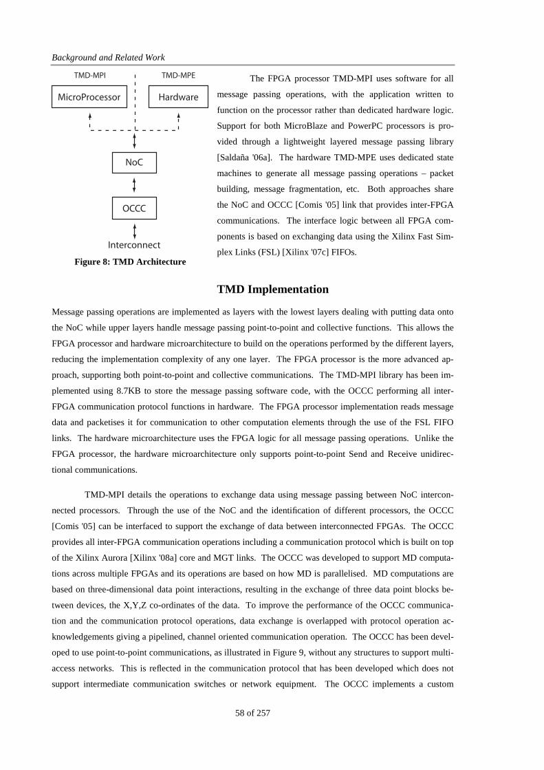
Background and Related Work
58 of 257
The FPGA processor TMD-MPI uses software for all
message passing operations, with the application written to
function on the processor rather than dedicated hardware logic.
Support for both MicroBlaze and PowerPC processors is pro-
vided through a lightweight layered message passing library
[Saldaña '06a]. The hardware TMD-MPE uses dedicated state
machines to generate all message passing operations – packet
building, message fragmentation, etc. Both approaches share
the NoC and OCCC [Comis '05] link that provides inter-FPGA
communications. The interface logic between all FPGA com-
ponents is based on exchanging data using the Xilinx Fast Sim-
plex Links (FSL) [Xilinx '07c] FIFOs.
TMD Implementation
Message passing operations are implemented as layers with the lowest layers dealing with putting data onto
the NoC while upper layers handle message passing point-to-point and collective functions. This allows the
FPGA processor and hardware microarchitecture to build on the operations performed by the different layers,
reducing the implementation complexity of any one layer. The FPGA processor is the more advanced ap-
proach, supporting both point-to-point and collective communications. The TMD-MPI library has been im-
plemented using 8.7KB to store the message passing software code, with the OCCC performing all inter-
FPGA communication protocol functions in hardware. The FPGA processor implementation reads message
data and packetises it for communication to other computation elements through the use of the FSL FIFO
links. The hardware microarchitecture uses the FPGA logic for all message passing operations. Unlike the
FPGA processor, the hardware microarchitecture only supports point-to-point Send and Receive unidirec-
tional communications.
TMD-MPI details the operations to exchange data using message passing between NoC intercon-
nected processors. Through the use of the NoC and the identification of different processors, the OCCC
[Comis '05] can be interfaced to support the exchange of data between interconnected FPGAs. The OCCC
provides all inter-FPGA communication operations including a communication protocol which is built on top
of the Xilinx Aurora [Xilinx '08a] core and MGT links. The OCCC was developed to support MD computa-
tions across multiple FPGAs and its operations are based on how MD is parallelised. MD computations are
based on three-dimensional data point interactions, resulting in the exchange of three data point blocks be-
tween devices, the X,Y,Z co-ordinates of the data. To improve the performance of the OCCC communica-
tion and the communication protocol operations, data exchange is overlapped with protocol operation ac-
knowledgements giving a pipelined, channel oriented communication operation. The OCCC has been devel-
oped to use point-to-point communications, as illustrated in Figure 9, without any structures to support multi-
access networks. This is reflected in the communication protocol that has been developed which does not
support intermediate communication switches or network equipment. The OCCC implements a custom
Interconnect
NoC
OCCC
MicroProcessor Hardware
TMD-MPI TMD-MPE
Figure 8: TMD Architecture
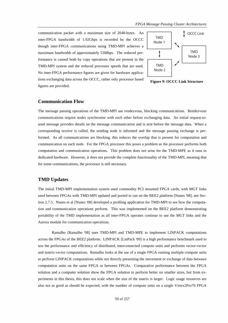
FPGA Message Passing Cluster Architectures
59 of 257
communication packet with a maximum size of 2048-bytes. An
inter-FPGA bandwidth of 1.92Gbps is recorded by the OCCC
though inter-FPGA communications using TMD-MPI achieves a
maximum bandwidth of approximately 53Mbps. The reduced per-
formance is caused both by copy operations that are present in the
TMD-MPI system and the reduced processor speeds that are used.
No inter-FPGA performance figures are given for hardware applica-
tions exchanging data across the OCCC, rather only processor based
figures are provided.
Communication Flow
The message passing operations of the TMD-MPI use rendezvous, blocking communications. Rendezvous
communications require nodes synchronise with each other before exchanging data. An initial request-to-
send message provides details on the message communication and is sent before the message data. When a
corresponding receive is called, the sending node is informed and the message passing exchange is per-
formed. As all communications are blocking, this reduces the overlap that is present for computation and
communication on each node. For the FPGA processor this poses a problem as the processor performs both
computation and communication operations. This problem does not arise for the TMD-MPE as it runs in
dedicated hardware. However, it does not provide the complete functionality of the TMD-MPI, meaning that
for some communications, the processor is still necessary.
TMD Updates
The initial TMD-MPI implementation system used commodity PCI mounted FPGA cards, with MGT links
used between FPGAs with TMD-MPI updated and ported to run on the BEE2 platform [Nunes '08], see Sec-
tion 2.7.5. Nunes et al [Nunes '08] developed a profiling application for TMD-MPI to see how the computa-
tion and communication operations perform. This was implemented on the BEE2 platform demonstrating
portability of the TMD implementation as all inter-FPGA operates continue to use the MGT links and the
Aurora module for communication operations.
Ramalho [Ramalho '08] uses TMD-MPI and TMD-MPE to implement LINPACK computations
across the FPGAs of the BEE2 platform. LINPACK [LinPack '09] is a high performance benchmark used to
test the performance and efficiency of distributed, interconnected compute units and performs vector-vector
and matrix-vector computations. Ramalho looks at the use of a single FPGA running multiple compute units
to perform LINPACK computations while not directly presenting the movement or exchange of data between
computation units on the same FPGA or between FPGAs. Comparative performance between the FPGA
solution and a computer solution show the FPGA solution to perform better on smaller sizes, but from ex-
periments in this thesis, this does not scale when the size of the matrix is larger. Logic usage resources are
also not as good as should be expected, with the number of compute units on a single Virtex2Pro70 FPGA
TMDNode 1
TMDNode 2
TMDNode 3
OCCC Link
Figure 9: OCCC Link Structure

Background and Related Work
60 of 257
not as high as achieved in experiments in this thesis on a Virtex2Pro30, even though both use single precision
floating point data. The additional interface overheads for connecting the computation units across the TMD-
MPI/MPE structures reduces the achievable performance while not reducing the implementation complexity
against a systolic array architecture.
TMD Restrictions
TMD-MPI performs communications between compute units through the use of both FPGA processor and
hardware microarchitectures however, restrictions exist for its correct use and operation. A major restriction
is the need to reconfigure the complete cluster for each new FPGA that is added [Saldaña '06b]. This is the
result of the hardcode NoC communication structures and results in the TMD-MPI only operating at 40MHz
to reduce the rebuild time for different topologies and per FPGA compute unit counts.
The TMD-MPI implementation requires the presence of at least one processor, which provides ac-
cess to external memory. The requirement of the processor increases resource usage while reducing the
amount of processing logic that can fit on each FPGA. The software implementation shares application
memory and message passing control memory. This limits application memory, while to support a large
number of processors on an FPGA, an upper limit of 64KB is applied to the amount of memory accessible to
each processor. Although the hardware microarchitecture can accelerate the FPGA processor communica-
tions, its limited message operations mean the software must still support and implement non-supported mes-
sage operations. The range of hardware message operations further limits the porting of an application to the
communications hardware microarchitecture if some of the required communications are not supported. The
use of a custom communication medium although well matched to the operations of the OCCC and NoC,
limits the ability to interface the nodes with a commodity computer system [Patel '06]. This is demonstrated
by the initial TMD-MPI architecture as data is moved to the FPGAs through the PCI bus on which they are
connected. To support communication with non-TMD-MPI and non-MGT compliant nodes, a bridging node
would be required to provide communication translation operations [Patel '06].
While the operations of TMD-MPI are similar to the operations that are being researched in this the-
sis, a number of specific and critical differences exist between them. The first is the use of switched Ethernet
against point-to-point MGT links between FPGAs. While point-to-point links are used by a number of re-
lated projects, they reduce the scalability of the system by increasing the need for routing logic on the FPGA
along with the prospect of increased communication delay for different algorithms which do not suit nearest
neighbour communications. The use of a dedicated and specific interconnect also increases the complexity of
interfacing the FPGAs with other non-OCCC based devices as bridging devices must be employed to inter-
connect the systems. Again, the ubiquity of Ethernet removes this overhead and allows for direct data ex-
change between commodity PCs and FPGA application logic. Secondly, the TMD system to operate cor-
rectly requires a large amount of data copying between the application and the NoC and then across the
OCCC link to interconnected FPGAs. The larger number of copies reduces the performance of TMD-MPI
and motivates the use of zero copy within this thesis’s research. For TMD-MPI to operate correctly, it re-
quires unique builds per board and this reduces the scalability of TMD-MPI as either lower clock frequencies
FPGA Message Passing Cluster Architectures
61 of 257
are required to reduce the time to implement a node or a limited number of nodes can be used. This gives
rise to a third difference between the approaches as the idea of scalability through both the switched Ethernet
network but also through a more dynamic approach to adding nodes is a distinct difference between the ap-
proaches. While TMD-MPI supports both hardware and software applications, its focus is more on how mes-
sage passing operates against how the application will use these resources. This is seen in the additional
copy operations that are required along with the reduce communication operations that are available for
hardware applications against software applications. The developed hardware API of the HDL MP API of
this thesis supports remote register transfer, independently of how the data exchange operations are per-
formed, providing another difference that exists between the solutions. Applications are able to exchange
data from both FPGA memory and application memory without needing to perform any additional opera-
tions. This more application against communication focus provides additional motivation for the develop-
ment of the hardware API. The structures of this thesis look to ensure only a single API needs to be used by
an application, with the development of a parametric interface to allow communications to be included or not
an additional contribution of the thesis. This ensures only a single interface is used, while TMD-MPI uses
two interfaces depending on whether software or hardware is used to provide the message passing data ex-
change operations. This means that different structures and testing operations are required to ensure an ap-
plication functions correctly and that modifications can be required to ensure an application that functions on
the processor will work correctly with the reduced amount of communications that are now available.
2.7.2 Reconfigurable Compute Cluster
The Reconfigurable Compute Cluster (RCC) is an investigation into creating a cost effective PetaScale FPGA
compute platform [Sass '07, Schmidt '08]. The RCC development is an extension of the Adaptable Compute
Cluster (ACC) project, which saw the development of the INIC for Beowulf clusters [Underwood '02]. The
investigations of the RCC solution look at the requirements for a PetaScale FPGA platform built of intercon-
nected distributed compute units.
Each node of the RCC is implemented as an FPGA which can use an FPGA processor or hardware
microarchitecture to perform computations and inter-FPGA communications. The message passing paradigm
is used for inter-FPGA communications with MGT point-to-point links connecting the distributed FPGAs.
As well as MGT links, an Ethernet network is present to allow a management computer interface with the
compute units of the cluster. The Ethernet network is also used by the FPGA communication logic to per-
form message passing operations which are not efficient on the MGT links e.g. broadcast. To reduce the ex-
pense of implementing the MGT point-to-point network, two novel ideas are present with the RCC. The first
sees the use of Serial Advanced Technology Attachment (SATA) cabling as the network fabric while the
second sees the development of an 8-point SATA attachment unit which provides each FPGA with a point-
to-point link to up to eight other compute units. The routing logic between compute units is implemented on
the FPGAs, removing the need for a costly high speed switch, reducing the cost of implementing the RCC
PetaScale FPGA cluster. However, using the reconfigurable logic of the FPGA in this way reduces the
Background and Related Work
62 of 257
amount of logic that can be used for algorithm computations. To provide performance, each FPGA node is
developed to contain a large amount of independent memory which is directly accessible to the FPGA. Both
memory accesses and network accesses are supported across the Processor Local Bus (PLB) and On-Chip
Peripheral Bus (OPB) SoC busses.
RCC Restrictions
The present RCC compute cluster architecture requires on-FPGA switching logic to allow an FPGA node
communicate with other FPGAs in the cluster. This consumes FPGA resources that could otherwise be per-
formed by commodity components. This is noted and investigations into using off-chip switches are pro-
posed. For correct operation, the RCC requires two networks, the MGT point-to-point network and the
Ethernet network. The use of two networks requires additional logic either on the FPGA or on the FPGA
development board to support both networks. The use of two networks pose a problem for the message pass-
ing applications as either an explicit communication is called for a given network or decision logic is used to
select which network a communication is to use based on the message passing communication that is re-
quested. This increases complexity of the interconnect and motivates looking at using a single interconnect
to support inter-FPGA communications.
2.7.3 SMILE
Scientific Parallel Multiprocessing based on Low Cost Reconfigurable Hardware (SMILE) [Castillo '08,
Pedraza '08] looks at using FPGA compute nodes for accelerating scientific data processing, in particular
content-based retrieval. Each SMILE cluster node is an XUP-V2P development board [Xilinx '05] intercon-
nected with neighbouring FPGAs using MGT point-to-point links across a SATA network. The message
passing programming paradigm is used across the FPGAs though only send and receive operations are sup-
ported. Message passing operations use the FPGA embedded PowerPC processor running Linux and
LAM/MPI. Dedicated hardware microarchitectures are used to accelerate the content-based image retrieval
operations but the reconfigurable logic is not used to accelerate or perform message passing communications.
Data is exchanged between the processor and the hardware microarchitectures through FIFOs.
SMILE Interconnect
Each SMILE node consists of three point-to-point links which create a pseudo two-dimensional torus. Three
Aurora cores are used with routing logic between links provided using FPGA logic, creating a SMILE Com-
munication Element (SCE). The processor interfaces with the routing logic through the OPB bus with all
message data communicated across the links. No details on packet or node identity are present and the use of
a custom packet can be assumed.
FPGA Message Passing Cluster Architectures
63 of 257
SMILE Restrictions
The overall architecture of SMILE sees the use of a standard computer approach on an FPGA with the
reconfigurable logic used to accelerate computations when possible. This introduces inefficiencies to the
operating system and support for a complete implementation of LAM/MPI. The inter-FPGA routing logic
implementation requires reconfigurable logic that could otherwise be used to accelerate the application run-
ning across the SMILE FPGA cluster. The limited routing of three point-to-point links limits the SMILE
cluster to 32 FPGAs while the use of SATA connectors limits the ability to interface the cluster with com-
modity computers.
2.7.4 FHPCA
The Field Programmable High Performance Computer Architecture (FHPCA) is a 64-node FPGA-based par-
allel supercomputer [Baxter '07, Baxter '08], similar in architecture to RCC. The FHPCA investigates the use
of commodity components for developing an FPGA supercomputer which is able to process real world high
performance computations, while not introducing a large learning curve to use the available performance.
The FHPCA has been used to accelerate a number of different algorithms including Molecular Dynamics and
Genome Sequencing [Storaasli '08] as well as Monte Carlo financial computations [Tian '08].
FHPCA consists of 32 compute nodes split into two sets of 16, with each compute unit in a set con-
sisting of two Virtex4 attached FPGA drop-in cards attached to a computer across the system bus. Each set
consists of a different FPGA either a Nallatech Virtex4 LX160 or AlphaData Virtex 4 FX100, and all com-
pute nodes are housed in a blade centre. The microprocessor of the compute node runs Linux and uses MPI
for internode communication. The FHPCA consists of two networks, a point-to-point high speed FPGA net-
work and an Ethernet network to exchange data between the microprocessors of each compute unit. The
point-to-point network is a 2D torus with MGTs used to directly exchange data in the absence of any special
routing logic on the FPGA. This allows both networks operate independently however, the FPGAs are con-
figured as accelerators rather than compute nodes in the FHPCA. The point-to-point links only support near-
est neighbour communications and rely on the Ethernet network for all non-nearest neighbour communica-
tions.
FHPCA Communications
The FHPCA uses MPI as the communication model across the cluster however, details on the MGT network
communications are not reported only that point-to-point links provide the communication medium. The use
of message passing for the MGT links has to be assumed however no details on how data is exchanged on the
MGT is provided – hardware microarchitecture or FPGA processor. Tian and Benkrid [Tian '08] discuss the
FPGA communications and detail the use of the Co-Processor Development Kit that is used in connection
with the AlphaData FPGA nodes. This development kit abstracts the implementation from the physical op-
Background and Related Work
64 of 257
erations of the FPGA and as part of this abstraction, the use of MPI as the communication method is detailed.
FHPCA Restrictions
The limited amount of routing present on the MGT links limits its operation to nearest neighbour communi-
cations. If an algorithm requires a different communication pattern, either routing logic would be needed on
each FPGA, a different communication topology configured or the communications performed across the
Ethernet network. This requires the use and operation of two networks, with the Ethernet network required
to operate the host computers while the high-speed network only provides point-to-point FPGA communica-
tions. The Nallatech FPGAs require an additional FPGA per board to provide the MGT links as the Virtex4
LX chips do not provide MGT FPGA primitives. This is a further restriction within FHPCA, the need to
ensure each FPGA provides MGT links.
2.7.5 Research Accelerator for Multiple Processors
The Research Accelerator for Multiple Processors (RAMP) [Wawrzynek '07] is a multi-phase research pro-
ject investigating the programming of massively parallel multiprocessor systems [Wee '07]. RAMP Blue
[Schultz '06, Burke '08], the phase relevant to this thesis, looks at programming multi-board, multi-FPGA
CMP systems. RAMP investigations are motivated by the continuing rise in the number of processor cores
on a single chip die and the programming models that can be used to efficiently utilise these resources, when
10’s and 100’s of cores are present. To test this, RAMP Blue uses Unified Parallel C (UPC), an offshoot of
GASNet, (Global Address Space Network) [Bonachea '06] as the parallel programming language, with MPI
functionality supported. UPC supports shared memory programming principles while also allowing for ex-
plicit communications as part of the programming model. Burke et al [Burke '08] have looked at using MPI
as the programming model and found that although it does allow existing code operate across RAMP Blue, it
does not scale as efficiently as UPC.
To implement a 1,024 processor RAMP CMP system, the BEE [Chang '05] hardware has been de-
veloped, with multiple BEE nodes interconnected with each other across high speed point-to-point MGT
links. Each BEE node consists of five FPGAs, one control FPGA and four user FPGAs, with each user
FPGA designed to contain up to 16 MicroBlaze processors each running a copy of uCLinux [Dionne '08].
Each user FPGA is connected to two other user FPGAs and the control FPGA as well as up to four other
BEE FPGA nodes across 10GBase-CX4 Ethernet links, Figure 10. Each 10GBase-CX4 Ethernet link is im-
plemented by 4 bonded MGT links supported by XAUI (10Gb Attachment Unit Interface) interfaces allow-
ing for the use of commodity 10 Gigabit Ethernet switches in the future. Internode communications are built
on top of the communication libraries provided by uCLinux with both TCP and UDP packets supported
across RAMP. Each FPGA has access to external Dual Data Rate (DDR) Dual Inline Memory Module
(DIMM) memory modules which are used to store both data and operating system code for each FPGA proc-
essor. To achieve this and enforce the UPC programming model, the memory is segmented by hardware
memory interface logic into 256 MByte blocks for each processor.

FPGA Message Passing Cluster Architectures
65 of 257
Inter-node Interconnect
FPGA 0 FPGA 3
FPGA 1 FPGA 2
ControlFPGA
Intra-NodeInterconnet
Intra-NodeInterconnet
Intra-NodeInterconnet
Intra-NodeInterconnet
Figure 10: BEE2, RAMP node configuration showing FPGA communication topologies. Not shown are
the Control FPGAs off chip communication links nor the DDR memory banks of each FPGA node.
Further to memory segmentation hardware, each CMP node is implemented using a pseudo NoC,
SoC approach, with each processor interfaced to other processors across a crossbar switch. This switch uses
static routing to move Ethernet encapsulated packets between processors and across the XAUI interface and
multi-FPGA links. FIFO buffers are present at the ingress and egress of the crossbar switch to ensure packets
are not dropped as the crossbar becomes loaded with traffic. All communication packets are generated across
the FSL interface with FIFO buffers storing the data as it is routed onto the crossbar.
Control of each RAMP node is performed through the Control FPGA. The control FPGA provides
the interface to the user FPGAs for programming, monitoring functionality and application data uploading.
This is performed across an Ethernet network. This operational configuration is needed as no direct interface
is present between the user FPGAs and a management compute node however, the possible use of a
10Gigabit Ethernet switch is detailed as one of the reasons for choosing the XAUI interface.
RAMP Restrictions
No DMA operations are supported by the network control logic [Schultz '06], though support for this is being
examined by Burke et al [Burke '08]. Data is transferred through the processor to the network buffers for
communications. The use of DMA based network operations would increase the network bandwidth and
reduce communication latencies. The complexity of an individual RAMP node increases the time to build
Background and Related Work
66 of 257
and test the architecture. The building overheads have resulted in the system only operating across eight
nodes as opposed to the sixteen nodes that have been targeted. All interface operations are performed
through the control FPGA which acts as a bridge between an Ethernet network and the RAMP Blue envi-
ronment. To reduce the resource usage of each node and to support as many processors as possible, floating
point computations logic is shared between processors. This reduces the amount of floating point computa-
tions that can be performed on each node while sharing the resource will incur a further drop in the maximum
achievable performance.
2.7.6 Janus
Janus [Belletti '09] is a parallel multi-FPGA scientific platform dedicated to solving Monte Carlo computa-
tional physic simulations, specifically Spin Glass experiments. The Janus project is an update of the Spin
Update Engine (SUE) project [Cruz '01] which first proposed an FPGA solution, with its high parallelism, as
a platform that can make the Spin Glass experiments computationally feasible for very large simulations.
Spin Glass computations are embarrassingly parallel however, they are not efficient on commodity proces-
sors, taking years to compute practical simulations with this time reduced to months by using FPGAs.
A Janus node consists of sixteen computation Virtex4’s and a seventeenth communication FPGA
[Belletti '08]. The Spin computations are performed on variable bit width data ranges (3 to 10 bits) depend-
ing on the algorithm requirements. No floating point operations are required while with appropriate data in-
terleaving a high degree of parallelism is exhibited [Belletti '08]. Computation FPGAs are configured as a
4x4 grid with each FPGA directly connected to its nearest neighbour in a torus architecture as well as to the
communication node FPGA. The communication FPGA links a Janus node with a control computer across
Gigabit Ethernet. The communication FPGA is responsible for exchanging computation data with the man-
agement microprocessor which tabulates and computes new updated results that each FPGA processing ele-
ment will require to operate correctly [Cruz '01]. The management microprocessor directs the Spin computa-
tions by performing complex operations with communication using raw Ethernet packets. Apart from the use
of raw Ethernet packets, no details on a communication model are provided although to allow other algo-
rithms use the Janus platform, investigations into the use of a model are ongoing [Belletti '06]
Janus Restrictions
Presently, Janus does not provide a communication model that will easily allow different applications to
communicate with each other or to map across the FPGA logic. FPGA nodes are not connected with external
memory, instead relying on the Block RAM memory of an FPGA. This limits the scope of algorithms that
can be accelerated with Janus while Spin computation details talk about the need to exchange data with the
management microprocessor frequently to perform the computations. This would limit the scalability of the
Janus environment and the number of nodes that can be connected to each other. As the management micro-
processor is necessary for Janus, no details are given on whether each Janus node can communicate with each
other; though the use of Ethernet would suggest, this should be feasible if not yet investigated.

FPGA Message Passing Cluster Architectures
67 of 257
2.7.7 Related Work Discussion
The different related work projects have highlight additional areas of interest and motivation for looking at
the use of switched Ethernet to interconnect the distributed hardware application microarchitectures, the need
to only support a single network across all interconnected devices. While the use of MGTs is becoming the
interface of choice, additional interconnects are required to operate and interface with the FPGAs – PCI inter-
face for TMD-MPI, switched Ethernet control network for RCC, RAMP, FHPCA. The overheads of operat-
ing two interconnects increases the implementation cost of these solutions while scalability is hindered as
each additional FPGA needs to interface with multiple networks, which may have different scaling character-
istics. By removing the overheads of additional networks, the feasibility of using switched Ethernet to sup-
port distributed computations while also reducing operational complexity will be demonstrated. This pro-
vides a contribution for the research of this work. Reducing the number of interconnects makes the use of
switched Ethernet and its ubiquity a useful feature.
The use of FPGA logic to support the networking logic also allows for scalability in the range of
FPGAs that can be used. MGT links while able to operate at a higher frequencies as they are pre-fabricated
primitives of the FPGA, are not present on all FPGAs which results in the need to use specific FPGAs. By
using switched Ethernet, the range of FPGAs that are usable is increased, increasing the scalability and appli-
cability of its use. The implementation of an Ethernet MAC on an FPGA will use a certain amount of the
available logic however, these overheads are offset against the use of MGT links as there is a need to imple-
ment interface and possibly routing logic with MGT links for their correct operation. Along with the re-
source usage requirements, a further issue with using MGTs, as highlighted by the FHPCA project, is the
need to use specific FPGAs to ensure inter-FPGA communications are supported. For the FHPCA project,
this increases the number of FPGAs that are needed with a special FPGA included for communication pur-
poses only. The need to support additional FPGAs increases the complexity of using and operating the inter-
connected FPGAs. Along with requiring additional FPGAs, there is an increased risk of failure as the more
devices that are needed, the greater the risk that one will not function correctly.
From the related projects, FPGA processors are the main approach used to support message passing
operations, while projects looking at using dedicated message passing hardware solutions are not as common.
This is against details presented as background information related to the use of network offload operations
which would suggest that the use of the hardware approach would provide performance advantages. The
decision as to which to use provides additional motivation and contribution for this research, allowing for an
investigation into both approaches to see how they operate and behave across switched Ethernet. A compari-
son of each approach and its performance for supporting distributed hardware application microarchitectures
is of interest so that it is possible to know the performance differences that are present and what consequence
these differences may have on an applications performance. There is a need for this information as each of
the related work approaches is looking to use high speed MGT networks yet are not able to say if the ap-
proach they are using for exchanging data across them is appropriate and efficient.

Background and Related Work
68 of 257
From TMD-MPI, a scalability issue arises if static structures are used to support the routing of data
between FPGAs. For TMD-MPI this required the use of slower clock frequencies and increased place-and-
route operations. Using a more dynamic approach to informing the FPGAs of there identities and routing
structures should reduce this problem. From the other projects, no details on the use of a dynamic approach
to node identity is provided so the use of a static approach is assumed. This would impact scalability as each
FPGA would require a specific implementation and with the overhead of design implementation times, only a
limited number of FPGAs could be supported. This is a further problem for FHPCA where the increased
number of FPGAs results in higher implementation overhead. As part of the research, the use of a more dy-
namic approach, similar to that of MPI, will be looked at to see if it is possible to use the same FPGA design
on multiple devices without the overhead of unique builds to support different architectures.
2.8 Summary and Motivation
Details presented for background and related work provides the motivation for the development of the re-
search question of this research, FPGA cluster architecture using Message Passing and switch Ethernet is a
realistic and scalable architecture for performing remote register transfer operations between distributed
hardware application microarchitectures. This question has been developed through the different projects
that have been researched which look at parallelising applications across multiple compute units to increase
the computation performance that is achieved. The methods used to support this parallelism have also been
investigated, with message passing chosen as the programming model for exchanging data between the dis-
tributed hardware application microarchitectures.
Message passing through the provision of a standardised communication interface, MPI, provides
for a range of implementation approaches once the interface is similar. The provision of an interface aids the
development of a hardware API which can be used by a hardware application to access resources of an FPGA
along with exchanging data with distributed microarchitectures in a reliable and robust manner. Along with
the use of message passing, a number of different approaches for implementing MPI have been discussed
with a layered approach selected as it is suitable for both a hardware and software approach, along with not
overly burdening the resources of an FPGA. A layered approach also suits the inclusion or not of communi-
cations as once lower layers which are required implement necessary features, higher layers can either use
the features or not be included. As part of the interface for a hardware application, the ability to select the
communications which are available on an application by application basis further improves the scalability
and usability of the solution as resources are not ideally used, rather they are used as they are required for the
correct parallelisation of the application.
While a range of interconnects are possible between FPGAs, switched Ethernet has been chosen as
no research has been undertaken into using it as the sole interconnect between distributed hardware applica-
tion microarchitectures using message passing for supporting remote register transfers. While the use of spe-
cialised and dedicated interconnects based on MGTs have been detailed, the use of one of the predominant
interconnects in supercomputing [SC '09], was an area that has not been explored fully. This motivated re-

FPGA Message Passing Cluster Architectures
69 of 257
searching the use of switched Ethernet while features present with this solution including scalability and ro-
bustness were further reasons to look at using it against more dedicated MGT solutions.
Details on the motivation, contribution and direction of the research of this thesis have been pre-
sented. To perform this research, the design of a system which supports the message passing and communi-
cation requirements is necessary, with the next chapter detailing the design taking on board the range of dif-
ferent approaches that have been researched. Along with the message passing and communication require-
ments, the application interface requirements and experiments that are to be undertaken are also detailed. To
address the research question, two approaches to supporting remote register transfer operations are investi-
gated and compared, a dedicated hardware and dedicated processor approach, with design trade-offs and con-
cerns of each discussed as part of the overall experimental system design.


71 of 257
Chapter 3
Design
The background chapter has discussed the FPGA requirements of distributed hardware application microar-
chitectures along with detailing the motivation for looking at message passing and switched Ethernet as the
platform for supporting this. As part of motivation for why message passing and switched Ethernet were
chosen, details on how a range of systems which support distributed hardware application microarchitectures
and also typical FPGA acceleration platforms have been described. These solutions provided details on a
number of different aspects that a hardware application would expect of an FPGA platform including the
provision of an interface between the application logic and the board structures, and an easy to use interface
which supports the message passing transfer operations. Taking these details and those presented in the lit-
erature, this chapter describes the design of the platform which supports message passing across switched
Ethernet by distributed hardware application microarchitectures including the development of a hardware
application microarchitecture interface that supports the exchange of data and synchronisation between the
distributed application microarchitectures, with the interaction of the overall system illustrated in Figure 11.
To help with the design and operations of the overall remote register
transfer operations, a top down design style is used which starts by looking at
the operations of the hardware application microarchitecture interface, the
HDL MP API, before proceeding to look at the lower layers and operations
that these need to perform to support the exchange of data between the dis-
tributed hardware application microarchitectures.
To correctly support an applications operations, the HDL MP API
needs to provide a number of features including access to the memory of the
FPGA system, both external and internal, and to the communication system
which will perform the exchange and synchronisation of data between a de-
fined set of registers in remote FPGAs and commodity processors. Applica-
tion data needs to be transferred between memory structures and the control
logic of the two remote data paths need to be synchronised. These require-
Application
HDL MP API Interface
Message Passing Protocol Operations
Interconnect Protocol Operations
Interconnect
Figure 11: Architectural
operation design
Design
72 of 257
ments drive the design of a message passing API for an algorithm that is implemented across several FPGAs.
To support this from a programmer’s perspective across multiple FPGAs, the ability to create, control and
distribute data is required which is easy to use and follows the operations provided by the hardware digital
logic application interface. As well as supporting the exchange of data between distributed application mi-
croarchitectures, the use of a management node which is developed to support the sequential operations of a
fork-join algorithm is also detailed. To ensure usability, scalability and overall system robustness, a single
parallel programming model is used across the FPGAs and management node.
Parallel algorithms run across multiple computational elements require certain features to operate
correctly. These include the ability to easily send and receive messages between multiple interconnected
application microarchitectures, an ability to access and store large amounts of data, dynamic communication
operations as each algorithm has a different communication pattern, local memory storage as portions of the
data are reused frequently, arbitrary communication sizes from very small to very large and an ability to scale
easily for a given problem size. The HDL MP API has been developed to support these operations through
the provision of two operational interfaces, the interface signals which support message passing – the com-
munication interface – and the interface signals for local memory – the computation interface.
This thesis is concerned with investigating the feasibility of using switched Ethernet in conjunction
with message passing to support distributed hardware application microarchitectures. To support these op-
erations, two main approaches have been identified, a dedicated hardware communications microarchitecture
and a software FPGA processor. Through the use of the HDL MP API, which abstracts the programmer from
the underlying data exchange mechanism, it has been possible to investigated both approaches while not re-
quiring modifications to either the application of the interface. This is an advance on the operations of other
FPGA message passing approaches where distinct interfaces are required depending on whether a software or
hardware approach was being taken. Investigating hardware and software approaches allow for measuring
the feasibility of using message passing and switched Ethernet by providing details on the performance and
resource overheads across a range of implementations. If low performance is recorded against the use of
other solutions, this will influence the applicability of this approach to different applications while if the re-
source usage is too high, the ability to parallelise an application across a large number of FPGAs will be off-
set by the amount of parallel computations that can be performed on any one interconnected FPGA.
To evaluate the research question and allow for conclusions to be drawn, the following experimental
setup is being designed which will allow for experiments to be performed and measured. The setup consists
of multiple Ethernet enabled FPGA development boards interconnected by switched Ethernet, with a com-
modity PC management node used to talk to, initialise and perform any sequential operations that arise as
part of the algorithm. Experiments will look at measuring the performance of both the hardware message
passing microarchitecture and the software FPGA processor approaches. All operations are supported by the
reconfigurable logic of the FPGA. For the hardware microarchitecture this sees all message passing opera-
tions performed by the FPGA digital logic. For the software FPGA processor, the Xilinx MicroBlaze soft
FPGA processor is used with all message passing code written in C.

FPGA Message Passing Cluster Architectures
73 of 257
This chapter details operations each approach must perform to function correctly and allow for ex-
periments which are used to evaluate the research question. As part of the operations that are detailed, the
following aspects of the architectures are original to the design and aid in its operations and efficiencies
• The development of a scalable and parametric hardware API which can be tailored to the require-
ments of a hardware application, including the development of a hardware oriented API which can
include as required a range of collective communications. The provision of collective communica-
tions as needed on an application by application basis has not been demonstrated in hardware be-
fore.
• The development of a novel fragmentation algorithm which both improves and reduces the opera-
tions that need to be supported for exchanging messages between compute units.
• The use of direct memory access operations as part of the hardware microarchitecture which al-
lows both applications and the network access external DDR memory. This operation has been
discussed as part of both Underwood et al [Underwood '01c] and Fuentes [Fuentes '06] though nei-
ther have demonstrated it. This work demonstrates the operations and use of this approach.
• The general description and discussion of the architectures which support the remote register
transfer operations for a hardware application across switched Ethernet. Within the hardware ar-
chitecture, the use of direct packet insertion for control packets has not previously been detailed as
an approach to take. Details on performing this are provided along with concerns that arise when
using this approach.
3.1 Message Passing
Message passing is used by parallel algorithms to exchange data and perform synchronisation across multiple
application microarchitectures and will be used to perform the remote register transfer operations. The
FPGA’s digital logic performs message passing operations as directed by the application through the com-
munication interface of the HDL MP API, with different communication approaches that will be supported
shown in Table 1. The communication interface abstracts the interconnect from the application microarchi-
tecture through the provision of a range of message passing remote register transfer operations including
• Send and receive message functionality between microarchitectures on arbitrary compute units,
based on the communication patterns of the algorithm.
• Message passing communications exchanging application Block RAMs, application registers and
arbitrary sized messages.
• Ability to add or remove nodes easily to support different algorithm computation requirements.
• Collective communications which can be included on a per application basis.
As part of the message passing operations, two communication types are supported, point-to-point and col-
lective communications. Collective communications are built on top of the functionality of point-to-point
communications and are designed to be optional in the operations of the message passing data exchange op-
erations. Collective communications will be includable on an algorithm by algorithm basis to ensure an as
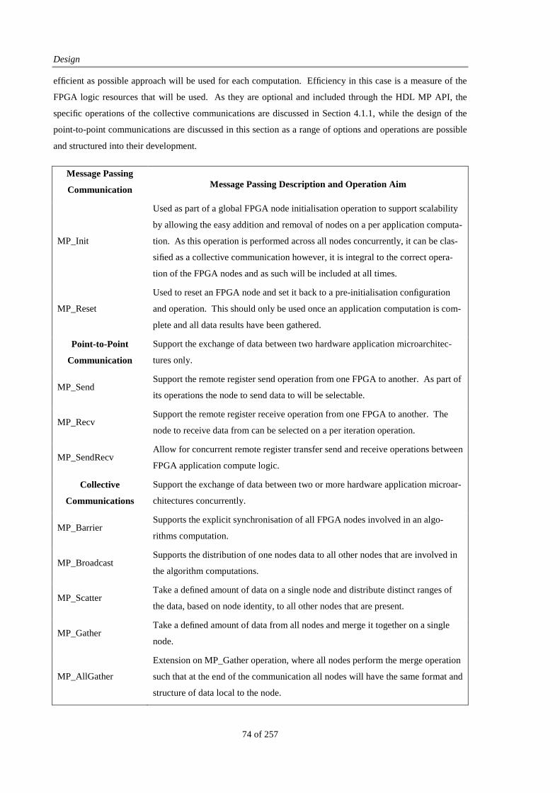
Design
74 of 257
efficient as possible approach will be used for each computation. Efficiency in this case is a measure of the
FPGA logic resources that will be used. As they are optional and included through the HDL MP API, the
specific operations of the collective communications are discussed in Section 4.1.1, while the design of the
point-to-point communications are discussed in this section as a range of options and operations are possible
and structured into their development.
Message Passing
Communication Message Passing Description and Operation Aim
MP_Init
Used as part of a global FPGA node initialisation operation to support scalability
by allowing the easy addition and removal of nodes on a per application computa-
tion. As this operation is performed across all nodes concurrently, it can be clas-
sified as a collective communication however, it is integral to the correct opera-
tion of the FPGA nodes and as such will be included at all times.
MP_Reset
Used to reset an FPGA node and set it back to a pre-initialisation configuration
and operation. This should only be used once an application computation is com-
plete and all data results have been gathered.
Point-to-Point
Communication
Support the exchange of data between two hardware application microarchitec-
tures only.
MP_Send Support the remote register send operation from one FPGA to another. As part of
its operations the node to send data to will be selectable.
MP_Recv Support the remote register receive operation from one FPGA to another. The
node to receive data from can be selected on a per iteration operation.
MP_SendRecv Allow for concurrent remote register transfer send and receive operations between
FPGA application compute logic.
Collective
Communications
Support the exchange of data between two or more hardware application microar-
chitectures concurrently.
MP_Barrier Supports the explicit synchronisation of all FPGA nodes involved in an algo-
rithms computation.
MP_Broadcast Supports the distribution of one nodes data to all other nodes that are involved in
the algorithm computations.
MP_Scatter Take a defined amount of data on a single node and distribute distinct ranges of
the data, based on node identity, to all other nodes that are present.
MP_Gather Take a defined amount of data from all nodes and merge it together on a single
node.
MP_AllGather
Extension on MP_Gather operation, where all nodes perform the merge operation
such that at the end of the communication all nodes will have the same format and
structure of data local to the node.
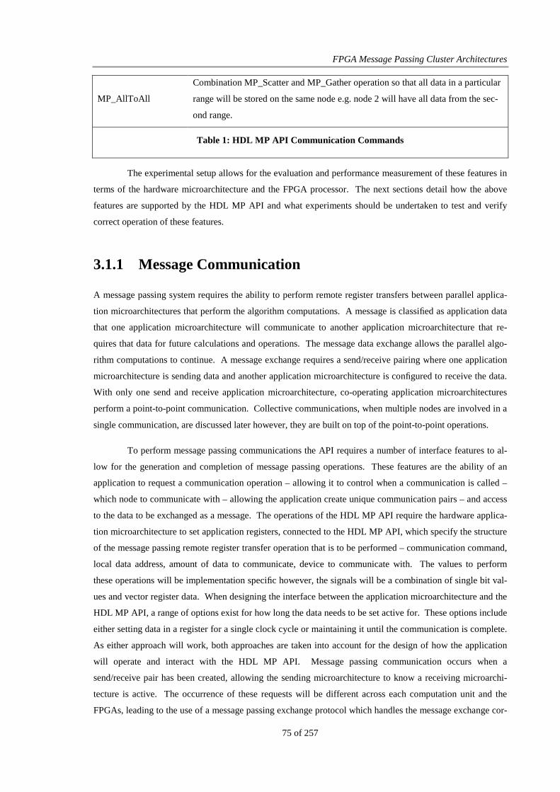
FPGA Message Passing Cluster Architectures
75 of 257
MP_AllToAll
Combination MP_Scatter and MP_Gather operation so that all data in a particular
range will be stored on the same node e.g. node 2 will have all data from the sec-
ond range.
Table 1: HDL MP API Communication Commands
The experimental setup allows for the evaluation and performance measurement of these features in
terms of the hardware microarchitecture and the FPGA processor. The next sections detail how the above
features are supported by the HDL MP API and what experiments should be undertaken to test and verify
correct operation of these features.
3.1.1 Message Communication
A message passing system requires the ability to perform remote register transfers between parallel applica-
tion microarchitectures that perform the algorithm computations. A message is classified as application data
that one application microarchitecture will communicate to another application microarchitecture that re-
quires that data for future calculations and operations. The message data exchange allows the parallel algo-
rithm computations to continue. A message exchange requires a send/receive pairing where one application
microarchitecture is sending data and another application microarchitecture is configured to receive the data.
With only one send and receive application microarchitecture, co-operating application microarchitectures
perform a point-to-point communication. Collective communications, when multiple nodes are involved in a
single communication, are discussed later however, they are built on top of the point-to-point operations.
To perform message passing communications the API requires a number of interface features to al-
low for the generation and completion of message passing operations. These features are the ability of an
application to request a communication operation – allowing it to control when a communication is called –
which node to communicate with – allowing the application create unique communication pairs – and access
to the data to be exchanged as a message. The operations of the HDL MP API require the hardware applica-
tion microarchitecture to set application registers, connected to the HDL MP API, which specify the structure
of the message passing remote register transfer operation that is to be performed – communication command,
local data address, amount of data to communicate, device to communicate with. The values to perform
these operations will be implementation specific however, the signals will be a combination of single bit val-
ues and vector register data. When designing the interface between the application microarchitecture and the
HDL MP API, a range of options exist for how long the data needs to be set active for. These options include
either setting data in a register for a single clock cycle or maintaining it until the communication is complete.
As either approach will work, both approaches are taken into account for the design of how the application
will operate and interact with the HDL MP API. Message passing communication occurs when a
send/receive pair has been created, allowing the sending microarchitecture to know a receiving microarchi-
tecture is active. The occurrence of these requests will be different across each computation unit and the
FPGAs, leading to the use of a message passing exchange protocol which handles the message exchange cor-
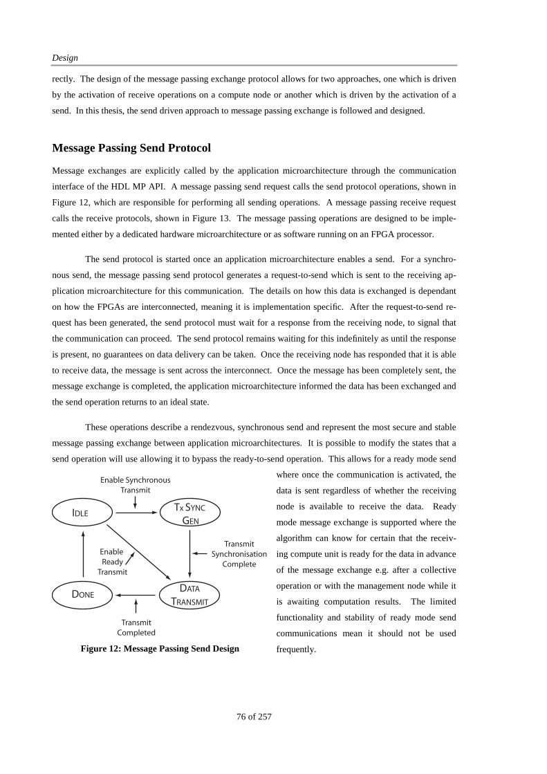
Design
76 of 257
rectly. The design of the message passing exchange protocol allows for two approaches, one which is driven
by the activation of receive operations on a compute node or another which is driven by the activation of a
send. In this thesis, the send driven approach to message passing exchange is followed and designed.
Message Passing Send Protocol
Message exchanges are explicitly called by the application microarchitecture through the communication
interface of the HDL MP API. A message passing send request calls the send protocol operations, shown in
Figure 12, which are responsible for performing all sending operations. A message passing receive request
calls the receive protocols, shown in Figure 13. The message passing operations are designed to be imple-
mented either by a dedicated hardware microarchitecture or as software running on an FPGA processor.
The send protocol is started once an application microarchitecture enables a send. For a synchro-
nous send, the message passing send protocol generates a request-to-send which is sent to the receiving ap-
plication microarchitecture for this communication. The details on how this data is exchanged is dependant
on how the FPGAs are interconnected, meaning it is implementation specific. After the request-to-send re-
quest has been generated, the send protocol must wait for a response from the receiving node, to signal that
the communication can proceed. The send protocol remains waiting for this indefinitely as until the response
is present, no guarantees on data delivery can be taken. Once the receiving node has responded that it is able
to receive data, the message is sent across the interconnect. Once the message has been completely sent, the
message exchange is completed, the application microarchitecture informed the data has been exchanged and
the send operation returns to an ideal state.
These operations describe a rendezvous, synchronous send and represent the most secure and stable
message passing exchange between application microarchitectures. It is possible to modify the states that a
send operation will use allowing it to bypass the ready-to-send operation. This allows for a ready mode send
where once the communication is activated, the
data is sent regardless of whether the receiving
node is available to receive the data. Ready
mode message exchange is supported where the
algorithm can know for certain that the receiv-
ing compute unit is ready for the data in advance
of the message exchange e.g. after a collective
operation or with the management node while it
is awaiting computation results. The limited
functionality and stability of ready mode send
communications mean it should not be used
frequently.
IDLETx SYNC
GEN
DATA
TRANSMITDONE
Enable SynchronousTransmit
TransmitSynchronisation
Complete
TransmitCompleted
Enable Ready
Transmit
Figure 12: Message Passing Send Design
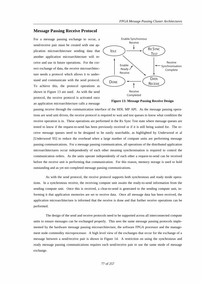
FPGA Message Passing Cluster Architectures
77 of 257
Message Passing Receive Protocol
For a message passing exchange to occur, a
send/receive pair must be created with one ap-
plication microarchitecture sending data that
another application microarchitecture will re-
ceive and use in future operations. For the cor-
rect exchange of data, the receive microarchitec-
ture needs a protocol which allows it to under-
stand and communicate with the send protocol.
To achieve this, the protocol operations as
shown in Figure 13 are used. As with the send
protocol, the receive protocol is activated once
an application microarchitecture calls a message
passing receive through the communication interface of the HDL MP API. As the message passing opera-
tions are send unit driven, the receive protocol is required to wait and test queues to know what condition the
receive operation is in. These operations are performed in the Rx Sync Test state where message queues are
tested to know if the request-to-send has been previously received or if it is still being waited for. The re-
ceive message queues need to be designed to be easily searchable, as highlighted by Underwood et al
[Underwood '05] to reduce the overhead when a large number of compute units are performing message
passing communications. For a message passing communication, all operations of the distributed application
microarchitectures occur independently of each other meaning synchronisation is required to control the
communication orders. As the units operate independently of each other a request-to-send can be received
before the receive unit is performing that communication. For this reason, memory storage is used to hold
outstanding and as yet not completed message passing communications.
As with the send protocol, the receive protocol supports both synchronous and ready mode opera-
tions. In a synchronous receive, the receiving compute unit awaits the ready-to-send information from the
sending compute unit. Once this is received, a clear-to-send is generated to the sending compute unit, in-
forming it that application memories are set to receive data. Once all message data has been received, the
application microarchitecture is informed that the receive is done and that further receive operations can be
performed.
The design of the send and receive protocols need to be supported across all interconnected compute
units to ensure messages can be exchanged properly. This sees the same message passing protocols imple-
mented by the hardware message passing microarchitecture, the software FPGA processor and the manage-
ment node commodity microprocessor. A high level view of the exchanges that occur for the exchange of a
message between a send/receive pair is shown in Figure 14. A restriction on using the synchronous and
ready message passing communications requires each send/receive pair to use the same mode of message
exchange.
Enable Ready
Receive
IDLERX SYNC
TEST
DATA
RECEIVEDONE
Enable SynchronousReceive
ReceiveSynchronisation
Complete
ReceiveCompleted
Figure 13: Message Passing Receive Design
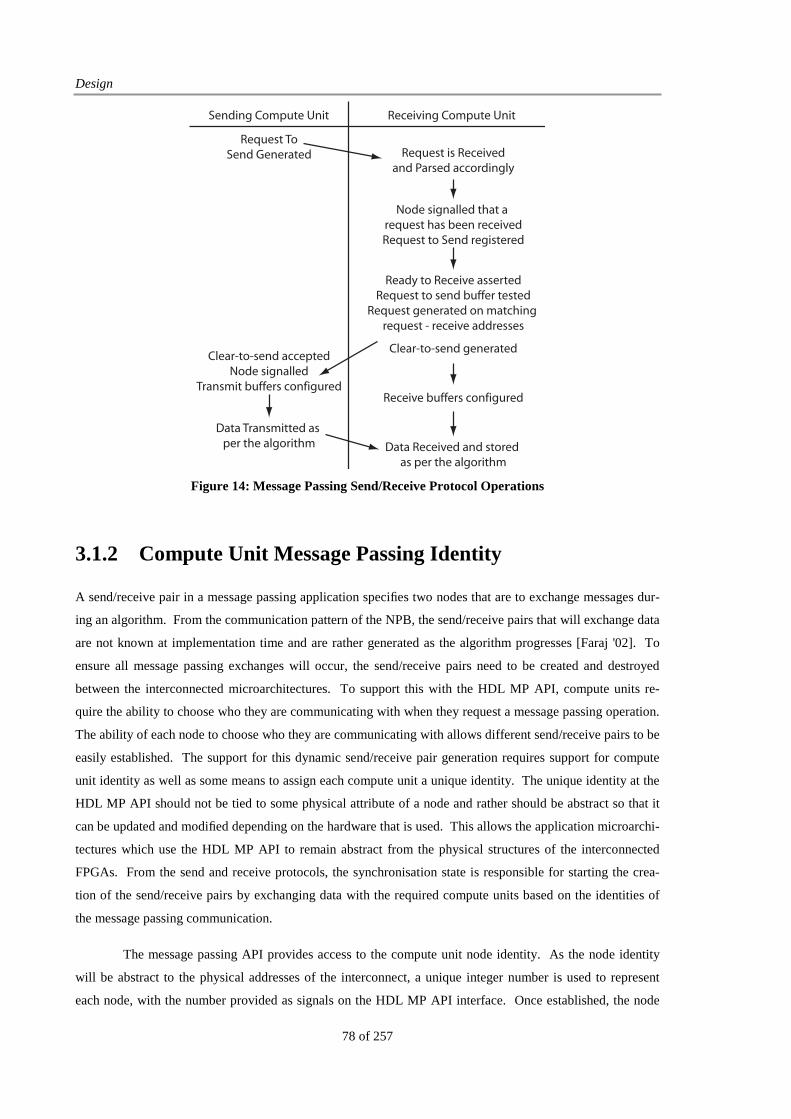
Design
78 of 257
3.1.2 Compute Unit Message Passing Identity
A send/receive pair in a message passing application specifies two nodes that are to exchange messages dur-
ing an algorithm. From the communication pattern of the NPB, the send/receive pairs that will exchange data
are not known at implementation time and are rather generated as the algorithm progresses [Faraj '02]. To
ensure all message passing exchanges will occur, the send/receive pairs need to be created and destroyed
between the interconnected microarchitectures. To support this with the HDL MP API, compute units re-
quire the ability to choose who they are communicating with when they request a message passing operation.
The ability of each node to choose who they are communicating with allows different send/receive pairs to be
easily established. The support for this dynamic send/receive pair generation requires support for compute
unit identity as well as some means to assign each compute unit a unique identity. The unique identity at the
HDL MP API should not be tied to some physical attribute of a node and rather should be abstract so that it
can be updated and modified depending on the hardware that is used. This allows the application microarchi-
tectures which use the HDL MP API to remain abstract from the physical structures of the interconnected
FPGAs. From the send and receive protocols, the synchronisation state is responsible for starting the crea-
tion of the send/receive pairs by exchanging data with the required compute units based on the identities of
the message passing communication.
The message passing API provides access to the compute unit node identity. As the node identity
will be abstract to the physical addresses of the interconnect, a unique integer number is used to represent
each node, with the number provided as signals on the HDL MP API interface. Once established, the node
Sending Compute Unit Receiving Compute Unit
Request ToSend Generated Request is Received
and Parsed accordingly
Node signalled that a request has been receivedRequest to Send registered
Clear-to-send generated
Ready to Receive assertedRequest to send buffer tested
Request generated on matching request - receive addresses
Receive buffers configured
Clear-to-send acceptedNode signalled
Transmit buffers configured
Data Received and stored as per the algorithm
Data Transmitted as per the algorithm
Figure 14: Message Passing Send/Receive Protocol Operations
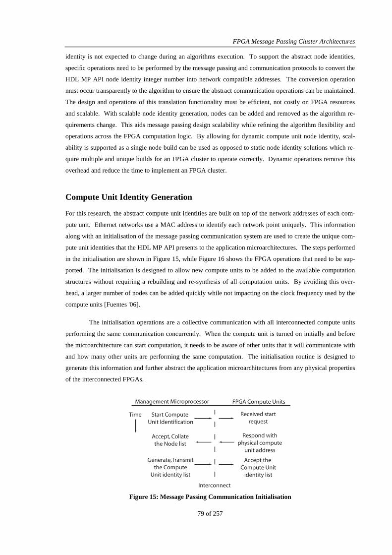
FPGA Message Passing Cluster Architectures
79 of 257
identity is not expected to change during an algorithms execution. To support the abstract node identities,
specific operations need to be performed by the message passing and communication protocols to convert the
HDL MP API node identity integer number into network compatible addresses. The conversion operation
must occur transparently to the algorithm to ensure the abstract communication operations can be maintained.
The design and operations of this translation functionality must be efficient, not costly on FPGA resources
and scalable. With scalable node identity generation, nodes can be added and removed as the algorithm re-
quirements change. This aids message passing design scalability while refining the algorithm flexibility and
operations across the FPGA computation logic. By allowing for dynamic compute unit node identity, scal-
ability is supported as a single node build can be used as opposed to static node identity solutions which re-
quire multiple and unique builds for an FPGA cluster to operate correctly. Dynamic operations remove this
overhead and reduce the time to implement an FPGA cluster.
Compute Unit Identity Generation
For this research, the abstract compute unit identities are built on top of the network addresses of each com-
pute unit. Ethernet networks use a MAC address to identify each network point uniquely. This information
along with an initialisation of the message passing communication system are used to create the unique com-
pute unit identities that the HDL MP API presents to the application microarchitectures. The steps performed
in the initialisation are shown in Figure 15, while Figure 16 shows the FPGA operations that need to be sup-
ported. The initialisation is designed to allow new compute units to be added to the available computation
structures without requiring a rebuilding and re-synthesis of all computation units. By avoiding this over-
head, a larger number of nodes can be added quickly while not impacting on the clock frequency used by the
compute units [Fuentes '06].
The initialisation operations are a collective communication with all interconnected compute units
performing the same communication concurrently. When the compute unit is turned on initially and before
the microarchitecture can start computation, it needs to be aware of other units that it will communicate with
and how many other units are performing the same computation. The initialisation routine is designed to
generate this information and further abstract the application microarchitectures from any physical properties
of the interconnected FPGAs.
Start Compute Unit Identification
Interconnect
Management Microprocessor FPGA Compute Units
Accept, Collatethe Node list
Generate,Transmitthe Compute
Unit identity list
Accept the Compute Unit
identity list
Received startrequest
Respond withphysical compute
unit address
Time
Figure 15: Message Passing Communication Initialisation
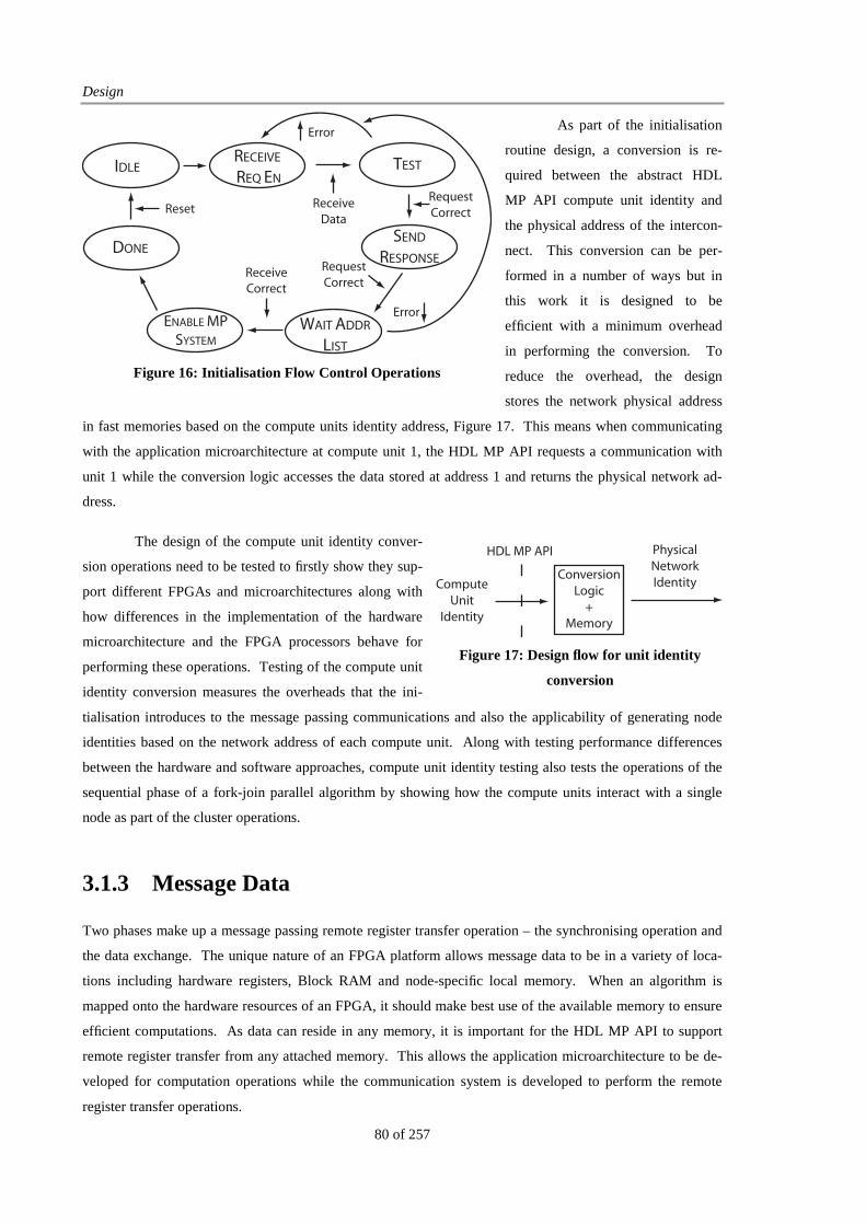
Design
80 of 257
As part of the initialisation
routine design, a conversion is re-
quired between the abstract HDL
MP API compute unit identity and
the physical address of the intercon-
nect. This conversion can be per-
formed in a number of ways but in
this work it is designed to be
efficient with a minimum overhead
in performing the conversion. To
reduce the overhead, the design
stores the network physical address
in fast memories based on the compute units identity address, Figure 17. This means when communicating
with the application microarchitecture at compute unit 1, the HDL MP API requests a communication with
unit 1 while the conversion logic accesses the data stored at address 1 and returns the physical network ad-
dress.
The design of the compute unit identity conver-
sion operations need to be tested to firstly show they sup-
port different FPGAs and microarchitectures along with
how differences in the implementation of the hardware
microarchitecture and the FPGA processors behave for
performing these operations. Testing of the compute unit
identity conversion measures the overheads that the ini-
tialisation introduces to the message passing communications and also the applicability of generating node
identities based on the network address of each compute unit. Along with testing performance differences
between the hardware and software approaches, compute unit identity testing also tests the operations of the
sequential phase of a fork-join parallel algorithm by showing how the compute units interact with a single
node as part of the cluster operations.
3.1.3 Message Data
Two phases make up a message passing remote register transfer operation – the synchronising operation and
the data exchange. The unique nature of an FPGA platform allows message data to be in a variety of loca-
tions including hardware registers, Block RAM and node-specific local memory. When an algorithm is
mapped onto the hardware resources of an FPGA, it should make best use of the available memory to ensure
efficient computations. As data can reside in any memory, it is important for the HDL MP API to support
remote register transfer from any attached memory. This allows the application microarchitecture to be de-
veloped for computation operations while the communication system is developed to perform the remote
register transfer operations.
ReceiveData
Error
Reset
Error
IDLERECEIVE
REQ EN
SEND
RESPONSE
ENABLE MPSYSTEM
RequestCorrect
TEST
RequestCorrect
WAIT ADDR
LIST
ReceiveCorrect
DONE
Figure 16: Initialisation Flow Control Operations
HDL MP API
ComputeUnit
Identity
ConversionLogic
+Memory
PhysicalNetworkIdentity
Figure 17: Design flow for unit identity
conversion

FPGA Message Passing Cluster Architectures
81 of 257
To achieve this, the API is required to provide an application with the ability to specify where data
is located. As data can be located as part of the algorithm implementation, the API must provide the ability
to interface this memory with the communication system. This interface should be easy to use while remain-
ing abstract to the physical communication interconnect. To allow data to reside in node local memory, the
message passing communication operations must be able to read the memory, while an application needs an
ability to specify which memory is to be communicated. By allowing data reside in either location, an algo-
rithm can use the best suited approach for its send/receive pair while not enforcing a single communication
approach. The ability of an application microarchitecture to specify a range of addresses for data requires the
ability to identify which is in local memory and which is in Block RAMs or registers of the application mi-
croarchitecture. The design of direct access to all memories of an FPGA stems from observations made by
Underwood et al [Underwood '01c] and Fuentes [Fuentes '06]. They observe that access to different memo-
ries would be advantageous in terms of performance and the amount of data that can be readily supported by
the microarchitectures.
3.1.4 Interface Communication Tailoring
The HDL MP API provides the message passing protocol which an algorithm employs through application
microarchitectures to perform parallel computation. Different algorithms will place a different emphasis on
the message passing communications that need to be supported [Faraj '02]. This can be seen as some algo-
rithms will require only point-to-point communications while others use different combinations of collective
and point-to-point communications. To meet these additional communication requirements, the HDL MP
API needs to be extensible, allowing new functionality to be added without requiring the modification of pre-
existing applications.
To support additional communication requirements above the typical point-to-point, the API needs
to be adaptable on an algorithm by algorithm basis. This allows each algorithm to choose additional commu-
nication operations, mainly collective operations, which are used solely by that algorithm. Collective com-
munications are a single communication which involves multiple compute units, e.g. Initialisation. The basic
operations of a message passing application use the send and receive operations to exchange data between the
application microarchitectures. Collective communications can be viewed as specialised operations which
extend send and receive functionality to support specialised communications across multiple compute units
concurrently. Each collective communication can be seen as a unique communication algorithm which con-
trols the send and receive state machines to support the collective communication.
Interface adaptability allows for the best use of the digital logic of an FPGA. As the resources of an
FPGA are limited, the ability to decide whether or not to include a communication operation allows for better
tailoring of the implementation to the communication requirements. As a given collective communication
operation may not be needed by an algorithm, its inclusion as part of the HDL MP API system increases the
logic resource usage of the message passing environment without directly benefiting the algorithms opera-
tions. To remove this, the HDL MP API is designed to be programmable so that for a given algorithm only

Design
82 of 257
necessary communication functionality is used and provided. This can be achieved by implementing the
collective communication as unique hardware components that can be included or not depending on the algo-
rithm requirements. The HDL MP API is designed to function correctly with or without the collective com-
munications inclusion.
To support the varied operations that an algorithm will need along with the different communication
operations that may or may not be included, the API requires a means to allow the algorithm to chose which
communication operation it is performing at any given time. The API is also required to inform the algo-
rithm when the communication is completed correctly, so that any further communications can be undertaken
while the completion of the communication allows the application microarchitecture reuse the message pass-
ing memory as it is no longer reserved for communications.
3.1.5 Communication Scalability
Scalability is an underlying requirement of parallel algorithms and implementations, with support for this
designed into the HDL MP API. For reconfigurable logic, scalability occurs in a number of ways from both
how the algorithm is implemented on the digital logic to the ease of scaling the algorithm across multiple
compute units. Scalability is required in a number of forms with the most common being the ability to add
and remove compute units as the algorithm requirements change. The ability to add compute units has been
described in Section 0. Other features that aid scalability relate to both the hardware application microarchi-
tectures and features that are supported by the HDL MP API.
The HDL MP API supports scalability through the send/receive communicating pairs that can be
created during the algorithm execution. This allows a single instance of an application microarchitecture be
configured to operate regardless of the number of connected compute units. With correct design, the compu-
tation logic only needs to be implemented once. For correct design, the application microarchitecture should
use the number of compute units present, as well as its own unit’s identity, to know who communications are
to be performed with. The extensibility of the HDL MP API allows a multitude of application microarchitec-
tures to use the same interface without requiring specific interfaces that would make them incompatible. This
design supports scalability as once the interface is understood, there is no additional learning or knowledge
required to utilise it to its fullest. Finally, scalability is supported by the different data memory locations that
are supported. This allows an application microarchitecture to be implemented to use the available memory
efficiently while the HDL MP API accesses the memories that exist on a given compute unit.
With these requirements in mind, the HDL MP API is designed to provide a parallel algorithm the
necessary features to allow it map and use the message passing communication paradigm running across
multiple interconnected FPGAs. The API provides the following features: an easy to use command and con-
trol interface which allows an algorithm select both the communication operations to be performed and to
whom the communication will occur with, an abstract environment where the application has no knowledge
of how the message passing exchange will proceed and an ability to communicate data from multiple differ-

FPGA Message Passing Cluster Architectures
83 of 257
ent memory locations as best suits the algorithm’s parallel requirements. These features have been identified
as required to allow an algorithm easily and efficiently map to the message passing paradigm running across
multiple FPGAs. Only point-to-point design requirements have been presented in-depth to this point. The
operations of collective communications are layered on top of those provided by the point-to-point function-
ality. Before presenting the design of a number of collective operations, the design which supports point-to-
point communications across Ethernet interconnected compute units is first detailed.
3.2 Interconnect Communication Operations
The described message passing operations are based on an abstract notion of how data is exchanged between
nodes. No single communication medium is expected or catered for, rather the operations are abstract but the
presence of an interconnect mechanism that will exchange the messages is assumed. To support these opera-
tions and to allow for experiments on the message passing system, the compute units and application mi-
croarchitectures need to be implemented to use an interconnect. For this research, the message passing op-
erations are built on top of switched Ethernet. Ethernet is used as it is a standardised commodity network
which has been shown to work and operate across FPGAs [Fallside '00, Lockwood '07]. Ethernet is a best
effort interconnect meaning it does not guarantee that data is exchanged correctly between compute units.
Using a switched interconnect supports scalability by making it easy to add compute units. However, unlike
point-to-point based message passing systems (TMD-MPI [Fuentes '06], RCC [Sass '07]), the switch in-
creases the complexity of exchanging messages between compute units.
From the message passing communication requirements, Ethernet requires two main features, the
ability to accept, communicate and decode message passing control data, synchronisation states from the
send and receive designs, Figure 12 and Figure 13, and the ability to access and stably transport all message
passing application data, data receive/transmit from Figure 12 and Figure 13. These requirements influence
the design and development of the internode communication solution. To reduce design complexity, certain
assumptions have been made including the use of a closed network consisting solely of the FPGAs and man-
agement node and that the only communications on the network are those generated by these interconnected
compute units as part of the parallel algorithm computations.
3.2.1 Communication Protocol
Ethernet is a best effort communication medium which requires the use of a communication protocol to pro-
vide guaranteed packet delivery. To ensure switches can be used as the interconnect medium, a protocol
which operates with Ethernet and provides the functionality discussed for the Message Passing protocols is
advantageous. Protocol choices include link layer protocols e.g. High-level Data Link Control (HDLC) [ISO
'07] or transport layer protocols e.g. TCP [Postel '81a]. The basic functionality provided by TCP – reliable
communications, packet order numbering operations – meet the communication requirements for exchanging
messages across Ethernet switches. This allows TCP operations to be used as the template for the develop-
Design
84 of 257
ment of a custom communication protocol for use by the communication system. A custom communication
protocol is developed as some of the operations of TCP are not needed based on the assumptions of the
communication domain. TCP supports port numbers to select applications that will communicate with each
other. The FPGA compute units are designed to support a single application microarchitecture. TCP has
support for out of order packet delivery. This is not practical on the FPGAs as too much information about
the communications would need to be maintained, reducing the amount of reconfigurable logic available to
the application microarchitectures. Other systems have also employed custom communication protocols to
improve communication efficiency without compromising the integrity of the data exchange e.g. Bruck et al
[Bruck '95] for the User-level Reliable Transmission Protocol (URTP). Aspects of the communication proto-
col are also based on scenarios that have been identified by Comis [Comis '05] for point-to-point data ex-
changes. This protocol takes into account algorithm communication patterns that have previously been iden-
tified. The communication protocol includes the following design characteristics:
• Sliding window communication protocol with defined window sizes
• In-order packet communication operations
• Window acknowledgement, error negative acknowledgement
• Explicit control packet generation
• One message data exchange at a time, many outstanding message requests
For the communication protocol to operate correctly, certain operations need to be performed on
messages that are communicated. Each message is split into communication windows with each communica-
tion window consisting of multiple packets. Splitting the data in this manner aids communication stability
while reducing the amount of data that needs to be exchanged if communication errors are discovered. A
communication window in this work is defined as a message segment such that a message is made up of one
or more message segments. Each message segment is made up of one or more network packets. To reduce
communication complexity, a message segment has a defined size which is common across the FPGA clus-
ter. The size of a message segment reflects both the need for efficient communication and the restricted
amount of resources present on the FPGA for handling and processing multiple packets. The communication
protocol details the exchange of network packets and message segments, with acknowledgement based flow
control used.
For a message passing exchange, both a sending and a receiving node are required to exchange data.
For the communication protocol, this requires the design of both sending and receiving operations which will
guarantee the exchange of message data. Each node’s operations occur asynchronously, with state informa-
tion exchanged as both explicit control packets and as packet header control information. Control data is
used to identify a given packet and its message segment.
This decouples the communication protocol from the physical interconnect implementation. For
both sending and receiving operations this results in a number of communication scenarios. The following
communication protocol scenarios have been identified for receive operations:
• Correct Segment Receive
• Control Packet Flow
FPGA Message Passing Cluster Architectures
85 of 257
• Packet Data Error
• Dropped Packet
• Receive Overflow
• Resent Message Segment
• Unexpected Resent Packet
Scenario 1 – Correct Segment Receive: A complete message segment has been received and processed. An
acknowledgement packet is generated to inform the sending node that the receiving node has received all
packets correctly. If there are no more outstanding message segments, the communication channel is
removed, awaiting the next communications.
Scenario 2 – Control Packet: Control packets are removed and decoded by the network operations. Two
main control packets are expected, those related to the message passing state machines and those related
to the network operations. All decoded message passing information is passed to the message state ma-
chines, while all network control packets update the communication state.
Scenario 3 – Packet Data Error: Data errors in packets can arise when data is being moved across the net-
work medium, with the packet information corrupted. A packet error, as caught by an error in the Cy-
clic Redundancy Check (CRC) field, says some data is wrong in the packet. In Ethernet packets, it is not
possible to tell what error has occurred. This makes the packet worthless and it is silently dropped while
the resending of the correct packet is awaited. Silent packet dropping is caught by the communication
protocol as either no acknowledgement will be generated causing a message segment resending or the
next packet that is received will be an out-of-order packet.
Scenario 4 – Dropped Packet: Dropped packets occur for a number of reasons including interconnect con-
gestion and packet bit errors. Like packet data errors, dropped packets must be identified and the correct
packet resent. To identify out-of-order packets, each packet requires a packet number which identifies
the packet within the message segment. To reduce the overhead of dropped packets, negative acknowl-
edgements are generated once an out of order packet has been received correctly at the node. A negative
acknowledge improves communication performance by reducing idle time. Limited FPGA resources
mean no out-of-order packet information is stored, rather the complete retransmission of the data is re-
quired.
Scenario 5 – Receive Overflow: A receive overflow occurs when the network receives more data than it is
able to store. The issue relates to buffers within the network which temporarily store data before it is
written to the final buffers. As message data is lost, a receive overflow is handled in the same way as a
dropped packet requiring a resend of the entire packet. Packet testing can be maintained, so that packet
data can be checked and a negative acknowledge generated immediately, without needing to wait to re-
cord an out-of-order packet.
Scenario 6 – Resent Message Segment: Dropped packets must be retransmitted to ensure all message data
is communicated correctly. The receiving node waits for the packet to be resent before proceeding with
any further receive operations, enforcing an in-order packet operation. Resent packets should be identi-
fied as such to ensure the same packet is not received multiple times. This problem arises when the
transmitting node believes a dropped packet has occurred and retransmits its packets data.
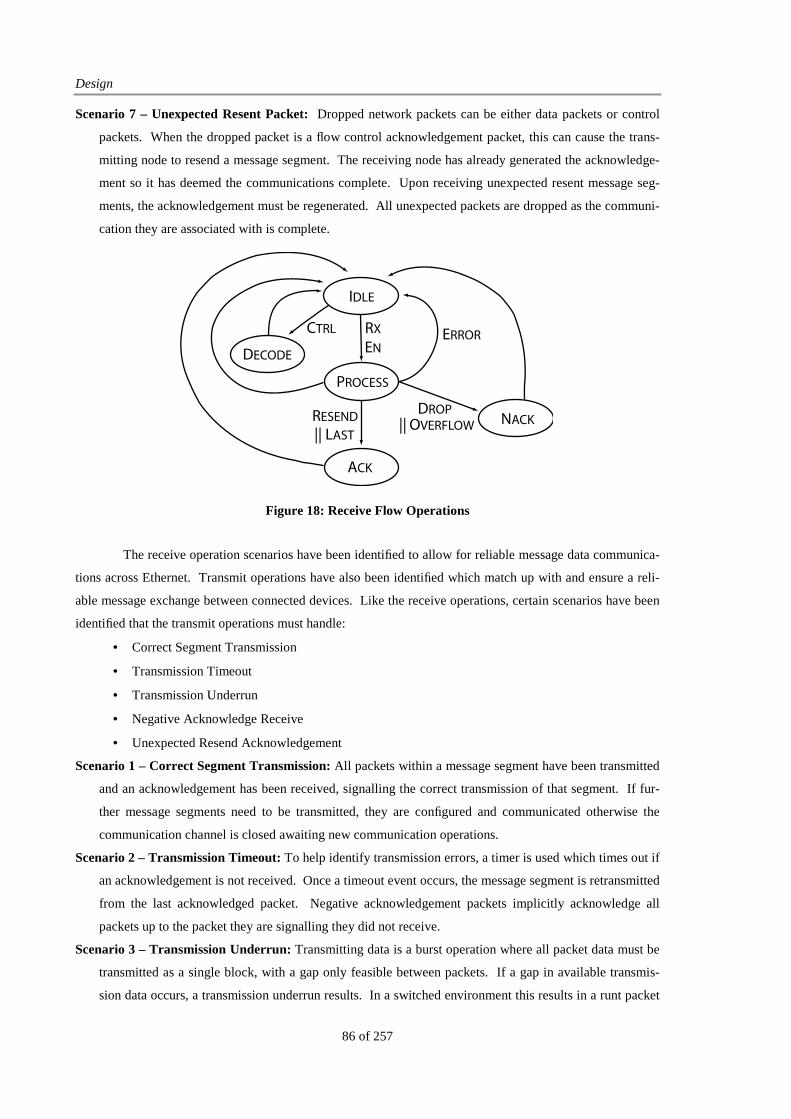
Design
86 of 257
Scenario 7 – Unexpected Resent Packet: Dropped network packets can be either data packets or control
packets. When the dropped packet is a flow control acknowledgement packet, this can cause the trans-
mitting node to resend a message segment. The receiving node has already generated the acknowledge-
ment so it has deemed the communications complete. Upon receiving unexpected resent message seg-
ments, the acknowledgement must be regenerated. All unexpected packets are dropped as the communi-
cation they are associated with is complete.
The receive operation scenarios have been identified to allow for reliable message data communica-
tions across Ethernet. Transmit operations have also been identified which match up with and ensure a reli-
able message exchange between connected devices. Like the receive operations, certain scenarios have been
identified that the transmit operations must handle:
• Correct Segment Transmission
• Transmission Timeout
• Transmission Underrun
• Negative Acknowledge Receive
• Unexpected Resend Acknowledgement
Scenario 1 – Correct Segment Transmission: All packets within a message segment have been transmitted
and an acknowledgement has been received, signalling the correct transmission of that segment. If fur-
ther message segments need to be transmitted, they are configured and communicated otherwise the
communication channel is closed awaiting new communication operations.
Scenario 2 – Transmission Timeout: To help identify transmission errors, a timer is used which times out if
an acknowledgement is not received. Once a timeout event occurs, the message segment is retransmitted
from the last acknowledged packet. Negative acknowledgement packets implicitly acknowledge all
packets up to the packet they are signalling they did not receive.
Scenario 3 – Transmission Underrun: Transmitting data is a burst operation where all packet data must be
transmitted as a single block, with a gap only feasible between packets. If a gap in available transmis-
sion data occurs, a transmission underrun results. In a switched environment this results in a runt packet
IDLE
PROCESS
RX
EN
CTRL
DECODE
RESEND
|| LAST
ACK
DROPNACK
ERROR
|| OVERFLOW
Figure 18: Receive Flow Operations
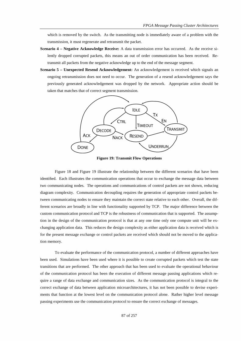
FPGA Message Passing Cluster Architectures
87 of 257
which is removed by the switch. As the transmitting node is immediately aware of a problem with the
transmission, it must regenerate and retransmit the packet.
Scenario 4 – Negative Acknowledge Receive: A data transmission error has occurred. As the receive si-
lently dropped corrupted packets, this means an out of order communication has been received. Re-
transmit all packets from the negative acknowledge up to the end of the message segment.
Scenario 5 – Unexpected Resend Acknowledgement: An acknowledgement is received which signals an
ongoing retransmission does not need to occur. The generation of a resend acknowledgement says the
previously generated acknowledgement was dropped by the network. Appropriate action should be
taken that matches that of correct segment transmission.
Figure 18 and Figure 19 illustrate the relationship between the different scenarios that have been
identified. Each illustrates the communication operations that occur to exchange the message data between
two communicating nodes. The operations and communications of control packets are not shown, reducing
diagram complexity. Communication decoupling requires the generation of appropriate control packets be-
tween communicating nodes to ensure they maintain the correct state relative to each other. Overall, the dif-
ferent scenarios are broadly in line with functionality supported by TCP. The major difference between the
custom communication protocol and TCP is the robustness of communication that is supported. The assump-
tion in the design of the communication protocol is that at any one time only one compute unit will be ex-
changing application data. This reduces the design complexity as either application data is received which is
for the present message exchange or control packets are received which should not be moved to the applica-
tion memory.
To evaluate the performance of the communication protocol, a number of different approaches have
been used. Simulations have been used where it is possible to create corrupted packets which test the state
transitions that are performed. The other approach that has been used to evaluate the operational behaviour
of the communication protocol has been the execution of different message passing applications which re-
quire a range of data exchange and communication sizes. As the communication protocol is integral to the
correct exchange of data between application microarchitectures, it has not been possible to devise experi-
ments that function at the lowest level on the communication protocol alone. Rather higher level message
passing experiments use the communication protocol to ensure the correct exchange of messages.
TIMEOUT
NACKACK
DONE
IDLE
RESEND
TX
ENCTRL
DECODE TRANSMIT
UNDERRUN
Figure 19: Transmit Flow Operations

Design
88 of 257
3.2.2 Control Packet Operations
To ensure the protocol operates correctly, control packets must be generated and communicated between the
compute units. Two approaches can be used, an implicit method where packet headers contain flow control
information or an explicit method where defined control packets are generated and exchanged between
nodes. To reduce implementation complexity, the design uses explicit control packet operations. This design
reduces the complexity of network specific data packets and reduces the complexity of the communication
protocols. For implicit control packets, the communication protocol would need to know that the compute
unit data is being exchanged with is the correct unit before it would append data to the packet header.
For implicit operations to function correctly, the
two compute units need to exchange data with each
other, so that the packet header information can be read
and tested. In a message passing application, this case
does not always occur. From Riesen et al [Riesen '06]
and Faraj et al [Faraj '02] and the ring communication
topology that can be used in matrix multiplication, it is
not possible to assume two compute units are exchanging
data to allow an implicit method operate correctly. With
multiple compute units present, the message passing ex-
change can create communication rings, as illustrated in Figure 20, where each node is transmitting data to
the next node without communicating any data back. So for the design, rather than supporting an implicit
approach that could introduce control packet generation delays2, an explicit approach is used at all times as
part of the communication protocols.
3.2.3 Ethernet Control Logic
Switched Ethernet is being used as the communications medium. To implement this correctly, an IEEE
802.3 standards compliant network controller is used. By using a compliant controller, it is possible to use
Ethernet switches as the interconnect medium as opposed to specialised point-to-point communication inter-
connects. With each compute unit implemented on an FPGA, this allows the network controller to be im-
plemented on the digital logic, rather than using a network ASIC controller. The use of a network controller
on the FPGA logic allows for a refinement of operations and investigations into the implementation of the
communication operations e.g. inline packet building, at-wire protocol processing [Jaganathan '03, Jiang '09].
Design trade offs however do exist by implementing the network control logic on the FPGA, with some of
the trade-offs between a dedicated ASIC controller and an FPGA implemented controller detailed in Table 2.
Network controller operations are independent of the higher layer operations however, the interfacing of
2 To know whether to generate a control packet or not, the implicit approach would need to wait for a defined time and know which compute units are communicating.
A B C
Data CommunicationPattern
Flow Control Communication Pattern
Figure 20: Message Passing
Communication Flow Layout

FPGA Message Passing Cluster Architectures
89 of 257
these layers with the Ethernet controller will depend on how the controller is implemented.
To evaluate the thesis hypothesis, the Ethernet controller is designed to be implemented on the
FPGA resources. Implementing the controller on the FPGA addresses some of the message passing scalabil-
ity concerns by allowing the same system design to be run across a wider range of Ethernet enabled FPGA
development boards than would have been the case if an external controller had been picked. The use of
MGT links was considered as part of this work. However, building the network controller to utilise these
interfaces limits the FPGAs that can be used as if an FPGA does not have an MGT, it will not be able to pro-
vide the necessary communication links.
Two approaches for implementing the message passing protocols are presented in this research, a
hardware message passing microarchitecture and a software FPGA processor. The use of the Ethernet con-
troller on the FPGA poses a few questions for each approach. For the FPGA processor, locating the Ethernet
controller on the FPGA does not provide any direct benefit. The software running on the FPGA processor is
designed to query and access the control logic of the Ethernet controller but has not been designed to use any
specialised logic that is present. Apart from the TMD-MPI, none of the other FPGA processor based mes-
sage passing solutions have used specialised architectures to support communication e.g. RCC, SMILE,
RAMP. For the software FPGA processor solution, the use of an on-FPGA controller poses a disadvantage
as it requires the use of reconfigurable logic that can not be used in a specialised manner. Limitations of the
available hardware for this project have prevented investigations into using an off-FPGA Ethernet controller
as part of the evaluation.
The hardware microarchitecture on the other hand is able to take advantage of the Ethernet control-
ler if it is located on reconfigurable logic. To reduce the complexity of the communication protocol, all op-
erations and decisions on the movement of data between the network and memories are taken as early as pos-
sible. To support early accessing and testing operations, at-wire testing operations are designed into the hard-
ware microarchitecture. This means that as data is received by the network controller, the packet information
is also tested to know the type of data that is being received and whether or not it is the correct data. By op-
erating in this manner, the overall complexity of the hardware microarchitecture is reduced. From previous
research into hardware optimised communication controllers [Bellows '02, Jaganathan '03, Comis '05,
Schlansker '07, Jiang '09], it is expected that the hardware microarchitecture will benefit from operating on
the communication data directly as it is received at the network interface. Performing the communication
protocol operations as close to the wire or on a processor, does not change the operations that need to be per-
formed as the communication operations are separate and distinct to the message passing protocol operations
that exchange data between the application microarchitectures.

Design
90 of 257
External Network Controller
Internal Network Controller
Advantages
1. FPGA resources not used
2. Commodity Component
3. Easily interface multiple network channels
with the FPGA
1. Better network to application integration
2. Standardised Network to physical layer
interface e.g. MII for Ethernet
3. Can operate at network ingress reducing
higher layers function requirements
Disadvantages
1. More complicated PCB, more components
2. Requirement to rework FPGA-Ethernet
interface logic for different Network chips
3. Required to use functionality of the net-
work chip without ability to modify its be-
haviour
1. Consumes FPGA logic resources
2. Increases place and route times
3. Impact application clock frequencies
Table 2: Network Controller Design Location Considerations
3.2.4 Network Fragmentation Design
When communicating a message across the network, the data has to be packetised and fragmented so that it
will comply with network packet structures and the Maximum Transmission Unit (MTU) of the given inter-
connect. Table 3 lists the MTUs for a number of different networks. Packetisation is the operation of encap-
sulating data in a network compliant structure. As the amount of communication data can exceed the MTU,
the data is fragmented into compliant sizes and then packetised. Fragmentation is typically performed by
continuously splitting the data into maximum sized packets, with the final packet containing any outstanding
communication data e.g. IP [Postel '81b], TMD-MPI [Fuentes '06]. An updated design to the typical frag-
mentation approach is used by this work.
Maximum (Bytes) Minimum (Bytes) Control Data Size (Bytes)
10/100 Ethernet 1500 64 18
1 Gigabit Ethernet 9000 64 (512 Slot size) 18
Infiniband 4096 24 up to 126
SCI 256 24 32
Table 3: Interconnection Communication Sizes
To reduce the computational requirements of a receiving node and to remove padded packets from
the network, the fragmentation policy has been updated for the last two fragments. Typically, the last two
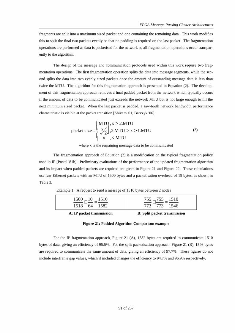
FPGA Message Passing Cluster Architectures
91 of 257
fragments are split into a maximum sized packet and one containing the remaining data. This work modifies
this to split the final two packets evenly so that no padding is required on the last packet. The fragmentation
operations are performed as data is packetised for the network so all fragmentation operations occur transpar-
ently to the algorithm.
The design of the message and communication protocols used within this work require two frag-
mentation operations. The first fragmentation operation splits the data into message segments, while the sec-
ond splits the data into two evenly sized packets once the amount of outstanding message data is less than
twice the MTU. The algorithm for this fragmentation approach is presented in Equation (2). The develop-
ment of this fragmentation approach removes a final padded packet from the network which typically occurs
if the amount of data to be communicated just exceeds the network MTU but is not large enough to fill the
next minimum sized packet. When the last packet is padded, a saw-tooth network bandwidth performance
characteristic is visible at the packet transition [Shivam '01, Barczyk '06].
<>>
>=
MTU,
MTU.1xMTU.2,
MTU.2x,
x2
xMTU
sizepacket (2)
where x is the remaining message data to be communicated
The fragmentation approach of Equation (2) is a modification on the typical fragmentation policy
used in IP [Postel '81b]. Preliminary evaluations of the performance of the updated fragmentation algorithm
and its impact when padded packets are required are given in Figure 21 and Figure 22. These calculations
use raw Ethernet packets with an MTU of 1500 bytes and a packetisation overhead of 18 bytes, as shown in
Table 3.
Example 1: A request to send a message of 1510 bytes between 2 nodes
1582
1510
64
10
1518
1500 =+ 1546
1510
773
755
773
755 =+
A: IP packet transmission B: Split packet transmission
Figure 21: Padded Algorithm Comparison example
For the IP fragmentation approach, Figure 21 (A), 1582 bytes are required to communicate 1510
bytes of data, giving an efficiency of 95.5%. For the split packetisation approach, Figure 21 (B), 1546 bytes
are required to communicate the same amount of data, giving an efficiency of 97.7%. These figures do not
include interframe gap values, which if included changes the efficiency to 94.7% and 96.9% respectively.
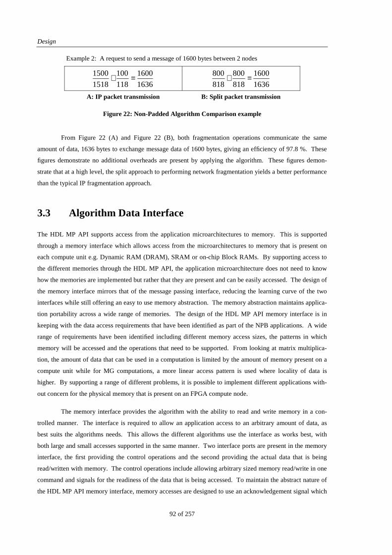
Design
92 of 257
Example 2: A request to send a message of 1600 bytes between 2 nodes
1636
1600
118
100
1518
1500 =+ 1636
1600
818
800
818
800 =+
A: IP packet transmission B: Split packet transmission
Figure 22: Non-Padded Algorithm Comparison example
From Figure 22 (A) and Figure 22 (B), both fragmentation operations communicate the same
amount of data, 1636 bytes to exchange message data of 1600 bytes, giving an efficiency of 97.8 %. These
figures demonstrate no additional overheads are present by applying the algorithm. These figures demon-
strate that at a high level, the split approach to performing network fragmentation yields a better performance
than the typical IP fragmentation approach.
3.3 Algorithm Data Interface
The HDL MP API supports access from the application microarchitectures to memory. This is supported
through a memory interface which allows access from the microarchitectures to memory that is present on
each compute unit e.g. Dynamic RAM (DRAM), SRAM or on-chip Block RAMs. By supporting access to
the different memories through the HDL MP API, the application microarchitecture does not need to know
how the memories are implemented but rather that they are present and can be easily accessed. The design of
the memory interface mirrors that of the message passing interface, reducing the learning curve of the two
interfaces while still offering an easy to use memory abstraction. The memory abstraction maintains applica-
tion portability across a wide range of memories. The design of the HDL MP API memory interface is in
keeping with the data access requirements that have been identified as part of the NPB applications. A wide
range of requirements have been identified including different memory access sizes, the patterns in which
memory will be accessed and the operations that need to be supported. From looking at matrix multiplica-
tion, the amount of data that can be used in a computation is limited by the amount of memory present on a
compute unit while for MG computations, a more linear access pattern is used where locality of data is
higher. By supporting a range of different problems, it is possible to implement different applications with-
out concern for the physical memory that is present on an FPGA compute node.
The memory interface provides the algorithm with the ability to read and write memory in a con-
trolled manner. The interface is required to allow an application access to an arbitrary amount of data, as
best suits the algorithms needs. This allows the different algorithms use the interface as works best, with
both large and small accesses supported in the same manner. Two interface ports are present in the memory
interface, the first providing the control operations and the second providing the actual data that is being
read/written with memory. The control operations include allowing arbitrary sized memory read/write in one
command and signals for the readiness of the data that is being accessed. To maintain the abstract nature of
the HDL MP API memory interface, memory accesses are designed to use an acknowledgement signal which
FPGA Message Passing Cluster Architectures
93 of 257
says when data is valid. Support for different RAM types means data will not always be valid on every ac-
cess clock cycle nor will the time overhead to access the memory be known in advance. This requires the
memory interface to signal valid data and when a memory access is complete so that any new algorithm ac-
cesses can be performed.
3.4 Management Node
For an algorithm mapped across the FPGAs, a means to access, transfer and manage the computations is re-
quired as seen with the sequential aspects of fork-join algorithms. This functionality is provided by the Man-
agement Node which provides a software microprocessor based interface to the FPGA nodes. Operations on
this compute node are designed to be lightweight in nature, such that the node provides a means to supply
computation data and display computation results. This requirement is met by a commodity PC, with all op-
erations written as software libraries that an application programmer can use. The design of the management
node software allows for the exchange of data between both systems. To support this, the send and receive
operations that have been detailed are supported as are some collective operations e.g. initialisation, barrier,
broadcast. The use of Ethernet as the system wide interconnection network aids the use of a PC as it is able
to directly interface and communicate with the FPGA nodes without the use of additional bridging logic.
Although the design of the management node sees it used to allow an application programmer com-
municate with the FPGA nodes, it does not mean it can not be used as part of the computations and system
wide operations. The provision of the management node means it can be used to perform operations that
would be very complex and resource intensive on an FPGA e.g. initialisation operations. This can be seen in
Figure 15 where the exchange of initialisation data assumes the presence of some form of management node.
Integration of the management node with the message passing operations supports scalability of the nodes
that are present and allows for an evaluation of the overheads of having the management node for both the
hardware microarchitecture and the software FPGA processor solutions. The microprocessor software mes-
sage passing API running on the management node allows for the exchange of data between the application
microarchitecture and itself. For a message passing solution, an assumption in the model is that only a single
node is responsible for managing the overall algorithm computations. This can be seen in the fork-join paral-
lelisation of an algorithm where one node must perform the sequential aspects of the code. For a message
passing system, only one compute unit can get node identity zero, as the first identity of an MPI application.
3.5 HDL MP API Evaluation Design
To measure the performance of the application programming interface and the remote register transfer opera-
tions, a number of experiments have been designed. These experiments measure the remote register transfer
operations that are provided by the HDL MP API as well as measuring the performance of both the dedicated
hardware microarchitecture and the software FPGA processor solutions that are used.

Design
94 of 257
For all experiments that are undertaken, an implicit aspect is the operations and support that the
HDL MP API provides the hardware application microarchitectures that are used in the tests. A direct ex-
periment to measure this is not possible apart from the diverse range of tests that have been undertaken
through its use. This sees the use of the same hardware application microarchitecture for each experiment
independently of the solution that is used to perform the remote register transfer operation. The hardware
application microarchitecture creates the experiments that are used to evaluate the performance of the imple-
mentation architectures. A wide range of experiments have been performed which attempt to measure spe-
cific operations and aspects of each architecture approach. The experiments can be classified into a number
of areas based on the aspects of the architectures that they measure.
The first set of experiments look at measuring the underlying operations and ability of the architec-
tures to support the exchange of data between the distributed hardware application microarchitectures. These
experiments stress test the various aspects of these operations including the operations of the network con-
troller and the message passing state transitions. These are performed first as the operation of the different
layers of the platform needs to be shown as operational before the other experiments can be undertaken. The
two stress tests measure the ability of the Ethernet controller to exchange data across the Ethernet switch and
the operations of the message passing protocol in exchanging message data between the interconnected nodes
using the architecture communication structures.
Interconnect Stability: Measurement of the stability and error / dropped packet rate of the Ethernet control-
ler across a range of switches, showing that it operates and functions correctly (Section 5.1.1).
Message Passing Protocol Experiment: Test of the message passing protocol, to see how it behaves under a
more randomised load and communication approach to test its ability to exchange application messages
(Section 5.1.2).
The second experiment set looks at the performance of the architectures over a range of benchmarks
Latency Measurement: Measurement of the latency to exchange minimum sized information between two
distributed hardware application microarchitectures (Section 5.2.1).
Message Passing Block RAM Exchange: Measures the performance of the HDL MP API to exchange ap-
plication specific Block RAM memories between two interconnected compute units (Section 5.2.2).
Bandwidth Measurement: Evaluate the performance of the HDL MP API and the architectures for support-
ing the exchange of arbitrary sized messages between two application microarchitectures (Section 5.2.3).
The scalability and programmability of the HDL MP API is tested. For this, a range of experiments
have been undertaken which are classified as operation experiments as they look at how the architectures
operate under increased node counts and communication approaches. As part of these experiments, collec-
tive communications are investigated.
Message Passing Initialisation: Test to see how well each system performs when data processing is per-
formed as part of the environment initialisation (Section 5.3.1). This experiment also shows how each
approach behaves when communicating with the management node.
Collective Operation Experiments: Additional tests that look at the scalability and expandability of the
HPL MP API interface. These experiments also measure the programmability of the HDL MP API in
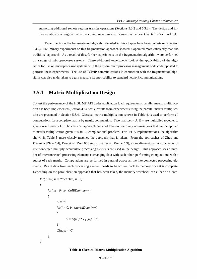
FPGA Message Passing Cluster Architectures
95 of 257
supporting additional remote register transfer operations (Sections 5.3.2 and 5.3.3). The design and im-
plementation of a range of collective communications are discussed in the next Chapter in Section 4.1.1.
Experiments on the fragmentation algorithm detailed in this chapter have been undertaken (Section
5.4.6). Preliminary experiments on this fragmentation approach showed it operated more efficiently than the
traditional approach. As a result of this, further experiments on the fragmentation algorithm were performed
on a range of microprocessor systems. These additional experiments look at the applicability of the algo-
rithm for use on microprocessor systems with the custom microprocessor management node code updated to
perform these experiments. The use of TCP/IP communications in connection with the fragmentation algo-
rithm was also undertaken to again measure its applicability to standard network communications.
3.5.1 Matrix Multiplication Design
To test the performance of the HDL MP API under application load requirements, parallel matrix multiplica-
tion has been implemented (Section 4.5), while results from experiments using the parallel matrix multiplica-
tion are presented in Section 5.3.4. Classical matrix multiplication, shown in Table 4, is used to perform all
computations for a complete matrix by matrix computation. Two matrices – A, B – are multiplied together to
give a result matrix C. The classical approach does not take on board any optimisations that can be applied
to matrix multiplication given it is an EP computational problem. For FPGA implementations, the algorithm
shown in Table 5 more closely matches the approach that is taken. From the approaches of Zhuo and
Prasanna [Zhuo '04], Dou et al [Dou '05] and Kumar et al [Kumar '09], a one dimensional systolic array of
interconnected multiply-accumulate processing elements are used in the design. This approach sees a num-
ber of interconnected processing elements exchanging data with each other, performing computations with a
subset of each matrix. Computations are performed in parallel across all the interconnected processing ele-
ments. Result data from each processing element needs to be written back to memory once it is complete.
Depending on the parallelisation approach that has been taken, the memory writeback can either be a com-
for( n =0; n < RowADim; n++)
{
for( m =0; m< ColBDim; m++)
{
C = 0;
for(i = 0; i< sharedDim; i++)
{
C = A[n,i] * B[i,m] + C
}
C[n,m] = C
}
}
Table 4: Classical Matrix Multiplication Algorithm

Design
96 of 257
plete result or a partially complete result that must be read back later. For ease of operation, the matrix mul-
tiplication performed in this thesis uses complete result writebacks. This reduces the number of memory
reads and writes that will occur, reducing the memory access overheads.
From the algorithm shown in Table 5, the design uses memory pre-fetching where data for a future
computation iteration is read in while no other memory access operations are ongoing. This hides memory
access latencies but does require memory buffers on the FPGA to store the pre-fetched data. The design re-
quires two memory buffers per processing element, one each for the A and B matrix data. For efficiency, the
memory buffers are part of the processing element to support the independent and concurrent accesses that
are required. For the computation results, data is stored in memory local to the processing elements to reduce
access overheads for the continued cycling of results data between the multiply-accumulate logic and the
partial result storage. Each processing element consists of a memory buffer which is used to store partial
result computations between iterations. The linear array consists of multiple processing elements which will
perform the computations. The design supports a single interface between the linear array and HDL MP API
memory interface. This reduces interface complexity and enforces an on chip shared memory style operation
where all computation logic shares access to the same memory at a high level. Internally in a processing
element, the operations reflect independent computation units that perform a defined set of operations on its
own data, independently of any other processing element. The operations of the linear array are shown in
Figure 23. Data reading is based on a transposed access from the standard configuration with the A matrix
wait(start)
read in B1[i…x-1]
for ( i = 0; i < Iteration Count - 1; i++ )
{
CONCURRENT
{
read B2[x…2x]
read in A[i… y-1]
for ( j = 0; j < y - 1; j++ )
{
compute A*B1[i…x-1]
}
} wait ( computation done && B read in complete)
B1 = B2
}
read in B
read in A
wait(computation complete)
write back C
Table 5: Linear Array Matrix Multiplication Algorit hm
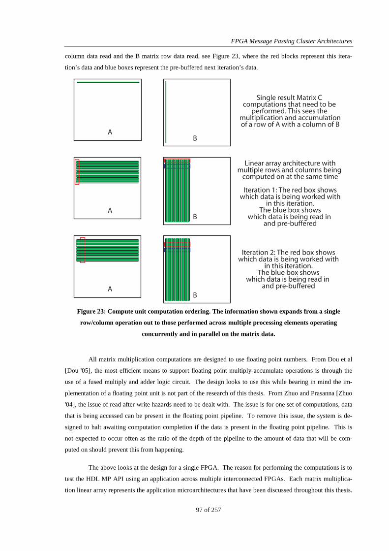
FPGA Message Passing Cluster Architectures
97 of 257
column data read and the B matrix row data read, see Figure 23, where the red blocks represent this itera-
tion’s data and blue boxes represent the pre-buffered next iteration’s data.
AB
AB
AB
Single result Matrix C computations that need to be
performed. This sees the multiplication and accumulationof a row of A with a column of B
Linear array architecture withmultiple rows and columns being
computed on at the same time
Iteration 1: The red box showswhich data is being worked with
in this iteration.The blue box shows
which data is being read in and pre-buffered
Iteration 2: The red box showswhich data is being worked with
in this iteration.The blue box shows
which data is being read in and pre-buffered
Figure 23: Compute unit computation ordering. The information shown expands from a single
row/column operation out to those performed across multiple processing elements operating
concurrently and in parallel on the matrix data.
All matrix multiplication computations are designed to use floating point numbers. From Dou et al
[Dou '05], the most efficient means to support floating point multiply-accumulate operations is through the
use of a fused multiply and adder logic circuit. The design looks to use this while bearing in mind the im-
plementation of a floating point unit is not part of the research of this thesis. From Zhuo and Prasanna [Zhuo
'04], the issue of read after write hazards need to be dealt with. The issue is for one set of computations, data
that is being accessed can be present in the floating point pipeline. To remove this issue, the system is de-
signed to halt awaiting computation completion if the data is present in the floating point pipeline. This is
not expected to occur often as the ratio of the depth of the pipeline to the amount of data that will be com-
puted on should prevent this from happening.
The above looks at the design for a single FPGA. The reason for performing the computations is to
test the HDL MP API using an application across multiple interconnected FPGAs. Each matrix multiplica-
tion linear array represents the application microarchitectures that have been discussed throughout this thesis.

Design
98 of 257
Using the HDL MP API, these microarchitectures will be interconnected to exchange computation data with
each other to perform a complete parallel matrix multiplication computation. The first aspect of a parallel
matrix multiplication is the manner in which data will be exchanged between microarchitectures. This influ-
ences the application microarchitecture as care is needed to support where data will be located. To ensure
support for a single result write back, data needs to be exchanged in a specific manner to support this. From
Schmollinger and Kaufmann [Schmollinger '02] the horizontal data decomposition supports this operation.
For inter application microarchitecture communication, a horizontal data decomposition allows for a ring
communication topology where every compute unit exchanges data with its neighbour, moving data in a ring
between compute units. To reduce the communication overheads, data exchange is performed concurrently
to the computations. This ensures that the next iteration’s data is already present before the next computation
commences and allows for more efficient computations. Matrix multiplication consists of two matrices that
are being multiplied. To support parallel computation, these matrices are divided across the available com-
putation resources as shown in Figure 25, for this work using the horizontal data decomposition.
FPGA2
FPGA1
FPGA0A0
A1
A2
B0 B2B1
A0 * B0 A0 * B1 A0 * B2
A1 * B0 A1 * B1 A1 * B2
A2 * B0 A2 * B1 A2 * B2
B Matrix, dividedinto 3 sub matrices
A Matrix, divided into 3
sub matrices
Figure 25: Matrix Computation Ordering. Computation s of the same colour are performed
concurrently across all FPGAs. For the design of the parallel matrix multiplication, the A matrix dat a
is maintained on the same FPGA while the B matrix data is exchanged across the ring topology to the
connected hardware application microarchitectures
For the matrix multiplication evaluation, a number of experiments have been performed. The initial
experiment saw the design of the classical approach, Table 4, which allows for testing of the HDL MP API,
application abstraction and the communication operations to ensure the ring topology, shown in Figure 24,
and the data decomposition are supported by the FPGAs. The second design sees the use of the linear array
as the computation microarchitecture, which is designed to use the communication topology and data decom-
position from the classical approach. Finally, an MPI version has been designed which is used to aid
Compute
Unit 0Compute
Unit 1
Compute
Unit n
Figure 24: Ring topology layout

FPGA Message Passing Cluster Architectures
99 of 257
verification and provide a performance comparison between the HDL MP API solution and a commodity
compute cluster solution.
3.6 Algorithm Design Considerations
When mapping an algorithm on to the computational resources of a processor and multiple interconnected
FPGAs, certain considerations should be given as to how this is done. All communications using the HDL
MP API exchange data using message passing. The message passing communication paradigm though may
not be the best approach for on-chip operations. The design and development of the HDL MP API has aimed
to maintain a large degree of freedom in how the algorithm is implemented on the computation resources,
with the programmer free to implement as efficient an approach as possible. This is achieved as the internal
computation operations of an algorithm are not restricted to using message passing to exchange data between
co-operating processing units running on the same FPGA. To allow the algorithm to scale, the programmer
can design and develop a single chip solution which uses the HDL MP API to interface with memory and
other board specific features. This implementation is then scalable through the message passing communica-
tion interface which allows the algorithm to exchange message data between compute units. This approach
can be seen from the matrix multiplication where messages are exchanged between compute units but the
linear array exchanges data between processing elements directly.
To provide an algorithm mapped onto multiple FPGAs, two features persist which can reduce the
computational performance. The first is the amount of FPGA digital logic an application has available for
performing parallel computations. The second is the manner in which data is laid out across both the mem-
ory and multiple nodes. The second aspect is specific to each algorithm and is not dealt with directly in this
work. However, the HDL MP API supports an efficient data layout through allowing both direct application
buffer message passing and access to the external memory of each FPGA node. To address the first parallel
aspect, the underlying operations of the HDL MP API are designed for efficiency, both in operational latency
overheads and logic resource usage. This latter option is evident from allowing the inclusion or not of collec-
tive communications depending on the algorithm’s communication requirements.
3.7 Summary
The design chapter has detailed the operations and structures that need to be developed to test the research
question. To provide a realistic, feasible and scalable approach to interconnecting FPGAs so that they sup-
port parallel algorithms, a range of different operations have to be supported. Details on the operations of the
message passing and switched Ethernet approaches including the protocols that are needed to support the
exchange of data in a scalable manner have been detailed. The structures and approaches that are being taken
reflect structures and approaches that have been presented as part of the background chapter, with operations
and concerns of a range of different systems integrated to develop the overall design of a realistic, feasible
and scalable message passing FPGA cluster which is interconnected across switched Ethernet. As part of the

Design
100 of 257
design requirements, the structures of the HDL MP API which is used to abstract a hardware application mi-
croarchitecture from the physical structures that perform the message passing operations has been detailed.
These design requirements include the interface operations that will let an algorithm scale to multiple FPGA
nodes while not restricting application operations. As part of the HDL MP API operations, memory interface
operations have been presented along with details on how it allows a parallel algorithm to access different
memory resources for the storage and mapping of data.
The information within this chapter details the design of the different aspects and how they are ex-
pected to be used for parallelising an algorithm across the FPGA logic. As well the structures that are re-
quired, details on a range of different evaluation experiments which will be used to answer the research ques-
tion have been presented. Each test evaluates different operations that have been identified for a range of
applications, while the design of a parallel matrix multiplication microarchitecture has been described which
looks to test the overall structures operations. The next chapter details the specific implementation concerns
for both the hardware and soft-processor approaches which allow an application to use the HDL MP API to
perform parallel computations.

101 of 257
Chapter 4
Implementation
The design to support feasible, realistic and scalable operations between distributed and interconnected
FPGA compute units using message passing and switched Ethernet has been presented in the last chapter. To
evaluate if this design will function and operate correctly for supporting distributed computations, it has been
implemented using both a hardware microarchitecture and a software processor approach. This chapter de-
tails the implementation operations along with some concerns and issues that have arise as part of this opera-
tion. The implementations look to take the hardware application microarchitecture remote register transfer
operations and exchange them with the different FPGA compute units that are interconnected to perform the
parallel computations. Two architectures have been implemented, a dedicated hardware message passing and
communication microarchitecture and a software FPGA processor architecture using the Xilinx MicroBlaze
processor [Xilinx '08b]. Each architecture interfaces with a HDL MP API enabled hardware application mi-
croarchitecture to support the remote register transfer operations of the parallel algorithm.
In this chapter, the implementation of each architecture is presented. The implementation of the
message passing operations can be layered on top of the communication operations that exchange the data.
The layered approach is used in this work, with the HDL MP API enabled application requesting various
remote register transfers as required by the algorithm. The two architectures used in this work are then re-
sponsible for exchanging this data between the interconnected FPGA nodes. Differences exist in the ap-
proaches that can be supported on the hardware and the software architectures in performing the register
transfer and communication operations. This work looks to implement efficient solutions for the given archi-
tecture to ensure a fair comparison evaluation can be made between the dedicated hardware microarchitecture
and the software FPGA processor.
To discuss and detail each implementation, this chapter is broken into a number of sections.
Through the use of the HDL MP API, it has been possible to have common operations that are performed
independently of the architectures themselves. These are detailed first as they must be known before discuss-
ing implementation specific architecture optimisations. From these common features, details of the message
passing and communication architecture are presented. This looks at how each architecture has been imple-

Implementation
102 of 257
mented to support the remote register transfer of data between distributed application microarchitectures us-
ing only the available hardware of the FPGA compute nodes. The software architecture and structures that
are used for the evaluation experiments are then detailed. This looks at how the MicroBlaze softprocessor
can be integrated with the HDL MP API to support remote register transfer between the distributed hardware
application microarchitectures. Matrix multiplication is being used as an evaluation application to test the
operations and performance of the HDL MP API in supporting a large parallel application which requires the
exchange of data between distributed application microarchitectures. As part of this, a high performance
linear array architecture has been implemented and detailed here. Finally, as part of the implementation, both
to support the benchmark experiments and the application evaluation the memory interface has been devel-
oped to support large external memories. The architecture and evaluation of this interface are presented.
4.1 Common Implementation Features
As part of the implementation which supports remote register transfer operations using message passing, a
number of features of both the hardware and software approaches are the same. The first of these is the HDL
MP API which is the hardware API between the hardware application microarchitecture and the message
passing and communication structures which exchange the application data between the distributed applica-
tions. To support this communication along with providing access to memory structures on the development
board, the HDL MP API has been implemented as a three channel interface, consisting of two communica-
tion interfaces and one memory interface. The communication interface allows for independent send and
receive operations while the memory interface supports access from the application microarchitecture to the
memory buffers of the FPGA.
For a remote register transfer operation to occur, the hardware application must request the neces-
sary communication – send, receive, barrier, etc. through the communication interface. The communication
interface consists of signals to support the send and receive remote register transfer operations – the size of
the data, who it is being communicated with, where the data is located – and command signals which select
the method of remote register transfer operation to be performed – send, receive, barrier, etc. While inde-
pendent send and receive signal interfaces are present for setting the communication parameters, a single
command interface is present for specifying the type of remote register transfer that is to be performed. A
single interface is presented as hardware restrictions require a hardware register to be update in a single func-
tional block – process or always statement. The use of a single command interface provides a more MPI like
communication interface along with supporting a range of communications more easily but results in a re-
duced ability to run many concurrent communications. The single command interface allows the program-
mer use the interface in a more programmed manner as for a given remote register transfer operation, only a
single interface needs to be understood and operated. To further reduce the interface complexity, Verilog
HDL pre-processor statements can be used to define the signal properties, allowing for a more software inter-
face feel to performing a remote register transfer, with Table 6 presenting some sample code used to perform
a message passing ready send.
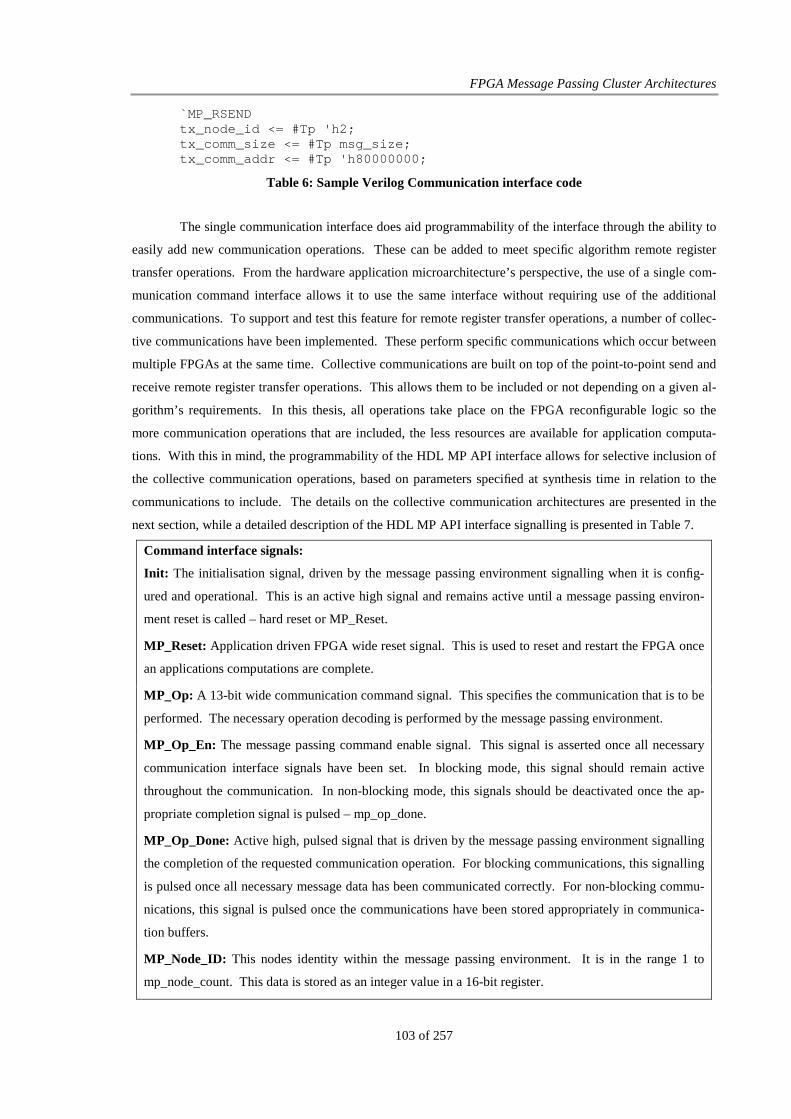
FPGA Message Passing Cluster Architectures
103 of 257
`MP_RSEND tx_node_id <= #Tp 'h2; tx_comm_size <= #Tp msg_size; tx_comm_addr <= #Tp 'h80000000;
Table 6: Sample Verilog Communication interface code
The single communication interface does aid programmability of the interface through the ability to
easily add new communication operations. These can be added to meet specific algorithm remote register
transfer operations. From the hardware application microarchitecture’s perspective, the use of a single com-
munication command interface allows it to use the same interface without requiring use of the additional
communications. To support and test this feature for remote register transfer operations, a number of collec-
tive communications have been implemented. These perform specific communications which occur between
multiple FPGAs at the same time. Collective communications are built on top of the point-to-point send and
receive remote register transfer operations. This allows them to be included or not depending on a given al-
gorithm’s requirements. In this thesis, all operations take place on the FPGA reconfigurable logic so the
more communication operations that are included, the less resources are available for application computa-
tions. With this in mind, the programmability of the HDL MP API interface allows for selective inclusion of
the collective communication operations, based on parameters specified at synthesis time in relation to the
communications to include. The details on the collective communication architectures are presented in the
next section, while a detailed description of the HDL MP API interface signalling is presented in Table 7.
Command interface signals:
Init: The initialisation signal, driven by the message passing environment signalling when it is config-
ured and operational. This is an active high signal and remains active until a message passing environ-
ment reset is called – hard reset or MP_Reset.
MP_Reset: Application driven FPGA wide reset signal. This is used to reset and restart the FPGA once
an applications computations are complete.
MP_Op: A 13-bit wide communication command signal. This specifies the communication that is to be
performed. The necessary operation decoding is performed by the message passing environment.
MP_Op_En: The message passing command enable signal. This signal is asserted once all necessary
communication interface signals have been set. In blocking mode, this signal should remain active
throughout the communication. In non-blocking mode, this signals should be deactivated once the ap-
propriate completion signal is pulsed – mp_op_done.
MP_Op_Done: Active high, pulsed signal that is driven by the message passing environment signalling
the completion of the requested communication operation. For blocking communications, this signalling
is pulsed once all necessary message data has been communicated correctly. For non-blocking commu-
nications, this signal is pulsed once the communications have been stored appropriately in communica-
tion buffers.
MP_Node_ID: This nodes identity within the message passing environment. It is in the range 1 to
mp_node_count. This data is stored as an integer value in a 16-bit register.

Implementation
104 of 257
MP_Node_Count: The node count for the number of FPGAs present within the message passing envi-
ronment. It will always start at 1, if the message passing environment has been correctly initialised.
The transmit interface signals:
Tx_Comm_Enable: Active high signal that is asserted by the network when communications are being
performed on the transmit data.
Tx_Comm_Complete: Active High, pulsed signal that is asserted when the end of the packet has been
reached. The assertion of this signal is used to inform the application that an individual packet of the
message has been transmitted and that it should behave accordingly. This signal is used when the appli-
cation has been charged with configuring and moving the data between the FPGA communication nodes.
Tx_Comm_Source: The base pointer to the node local buffer space that is to be used for the transmit
communication. This signal is latched concurrently to Tx_Comm_Enable.
Tx_Node_ID: The remote node identity that is to be communicated with. The necessary address trans-
lations are performed on this signal by the message passing control logic. A tag value can be associated
with the tx node identity to allow multiple remote register transfers with the same node.
Tx_Ready: Active high signal that informs the message passing system that the necessary data is present
and can be accessed accordingly.
Tx_Comm_Addr: Pointer to the starting address of the communication data. This is 32-bits wide with
any address above 0x80000000 assumed to reference local application buffers
Tx_Comm_Data: Local data buffer interface. The communication structures read the data from this
interface port. This is a 32-bit data signal.
Tx_Comm_Size: The message size in bytes that is to be communicated between the nodes. This is a
32-bit signal, allowing a message passing application to communicate any amount of data that may be
required.
Tx_Data_Delay: Not all connected memories present data immediately so to ensure correct data is
transferred, the application can specify the memory access delay ensuring correct data is operated on.
This is required if Block RAMs are interfaced with the transmit logic. A one cycle read delay is present
for all Block RAM data.
The receive interface signals:
Rx_Comm_Enable: Active high signal that is asserted by the network saying that data is being received
from the network and being written to the appropriate address, as specified by the original register trans-
fer request.
Rx_Comm_Complete: Active High, pulsed signal that is asserted when the end of the packet has been
reached. The assertion of this signal informs the application that an individual packet of the message has
been received. This signal is used when the application has been charged with configuring and moving
the data between the FPGA communication nodes.
Rx_Comm_Source: The base pointer to the local buffer space that is to be used to store received com-
munication data. This signal is active while Rx_Comm_Enable is asserted.

FPGA Message Passing Cluster Architectures
105 of 257
Rx_Node_ID: The remote node identity that data is to be received from. The necessary address transla-
tions are performed on this signal by the message passing environment. A tag value can be associated
with the rx node identity to allow multiple remote register transfers with the same node.
Rx_Ready: Active high signal that informs the message passing system that the receive logic is active
and that the data will be written in memory elements.
Rx_Comm_Addr: Pointer to the starting address of the communication data. This is 32-bits wide with
any address above 0x80000000 assumed to reference local application buffers
Rx_Comm_Data: Local data buffer interface. The communication data that is to be written into the
application local data storage structure. This is a 32-bit data signal.
Rx_Comm_Size: The amount of data, in bytes, that are to be received by this node as part of the re-
quested communication. This is a 32-bit interface port, allowing for arbitrary communication sizes.
Rx_Data_Delay: Any additional writing delays that will be present when data is being written into the
application local storage space.
Table 7: HDL MP API Communication interface signals
4.1.1 Collective Communication Implementation
Collective communications are communications that involve multiple nodes communicating with each other
concurrently to perform a single large remote register transfer operation. Each collective communication
operation is implemented as a unique dedicated state machine which controls and operates the point-to-point
communications to perform the prescribed remote register transfer operations. The development and imple-
mentation of each state machine has been strongly influenced by the collective communication operations of
MPICH 1.2 [MPICH '07]. While investigating MPICH implementations, only operations which do not use
temporary storage or limit the scalability of the system are investigated. This arises as in certain situations,
optimised versions based on the number of nodes are possible. To reduce the digital logic resource require-
ments, the use of optimised solutions based on the number of nodes was not used. Rather scalability of the
collective communications was used to choose between implementation methods. The hardware state ma-
chines, using the algorithm operations of MPICH as a template, have been implemented taking into account
the limited resources available on each FPGA node. By including collective communications, the application
programmer is freed to parallelise the algorithm across the FPGA resources as opposed to implementing
these remote register transfer operations. As part of the programmability of the HDL MP API, the different
collective communications can optionally be included for a given algorithm, ensuring an optimal communi-
cation approach is used. This is achieved through parameters which can be set on an application by applica-
tion basis at synthesis time. This supports scalability of the implementation as resources are not used unless
required and as shown by Faraj and Yuan [Faraj '02], collective communications are not always required but
are necessary for some algorithms to operate correctly.

Implementation
106 of 257
The collective communications are implemented on top of the point-to-point communication opera-
tions. This allows the same collective communication hardware to be used with both the hardware and soft-
ware message passing implementations. This aids in demonstrating the abstractions that the HDL MP API
supports between the message passing operations and the physical implementation that is used. The division
of collective and point-to-point communications also allows the implementations to focus on supporting
point-to-point communications primarily. This allows the software to remain lightweight while the hardware
collective state machines ensure the flexibility of the HDL MP API. The implementation details on different
collective communications which have been tested, through simulation, are presented. The initialisation op-
eration, described in 0, although a collective operation is not included here as it performs specific operations
that are connected to the hardware and software implementations. This allows each implementation, hard-
ware and FPGA processor, to most efficiently perform the initialisation operations.
For the collective communication implementation a number of conditions are enforced across all
communicating nodes. When a collective communication is requested, it creates an implicit synchronisation
point across all the compute nodes as the operation will only complete once all nodes have reached and per-
formed the communication. On any given node, a collective communication will not commence until all
point-to-point operations have completed. If any point-to-point communications are active, this means that at
least two nodes have not completed communications previous to the calling of the collective communication.
The operations of the collective communications are independent of the number of nodes that are present,
instead all operations have been generated, like the HDL MP API, not to enforce a particular limitation on
their use by an algorithm.
Barrier
A barrier communication is used by an algorithm to explicitly synchronise all nodes. This style of operation
would be used in fork-join parallelisation before results would be merged back together to ensure all compu-
tations are complete. A barrier achieves this by preventing further computations until all nodes have started
the barrier communication. To ensure this has happened, all nodes call the barrier which sees the exchange
of a zero sized message. The exchange of the message is performed concurrently on all nodes, using a mini-
mum amount of communications, based on knowledge of the state nodes are in. The barrier operation can
only complete once all nodes have correctly exchanged data with other barrier enabled nodes before they can
proceed with other operations. To perform a barrier efficiently, there is no requirement for all nodes to com-
municate with all nodes, rather each node only needs to exchange data with a subset of all the nodes. To
achieve this correctly, an iterative approach is used with each new iteration telling a node more about the
operations of other nodes that are involved. The iterative approach of barrier operations, limits the number of
communications to the log of the number of nodes that are performing the barrier The communication pat-
tern between nodes is based on an iteration mask and the nodes identity, such that each node communicates
with ((node identity + (2iteration+1 – 1)) % number of nodes). This operation is performed efficiently by using
shift operations to generate the mask value and a subtraction operation to perform the modulus if the addition
result is too large. After an iteration, a node is aware of what operations have been completed in relation to
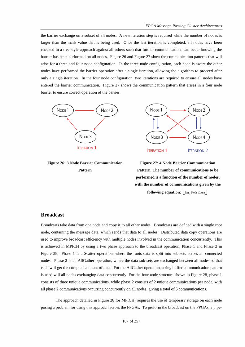
FPGA Message Passing Cluster Architectures
107 of 257
the barrier exchange on a subset of all nodes. A new iteration step is required while the number of nodes is
larger than the mask value that is being used. Once the last iteration is completed, all nodes have been
checked in a tree style approach against all others such that further communications can occur knowing the
barrier has been performed on all nodes. Figure 26 and Figure 27 show the communication patterns that will
arise for a three and four node configuration. In the three node configuration, each node is aware the other
nodes have performed the barrier operation after a single iteration, allowing the algorithm to proceed after
only a single iteration. In the four node configuration, two iterations are required to ensure all nodes have
entered the barrier communication. Figure 27 shows the communication pattern that arises in a four node
barrier to ensure correct operation of the barrier.
NODE 1 NODE 2
NODE 3
ITERATION 1
NODE 1 NODE 2
NODE 3 NODE 4
ITERATION 1 ITERATION 2
Figure 26: 3 Node Barrier Communication
Pattern
Figure 27: 4 Node Barrier Communication
Pattern. The number of communications to be
performed is a function of the number of nodes,
with the number of communications given by the
following equation: Count Node log2
Broadcast
Broadcasts take data from one node and copy it to all other nodes. Broadcasts are defined with a single root
node, containing the message data, which sends that data to all nodes. Distributed data copy operations are
used to improve broadcast efficiency with multiple nodes involved in the communication concurrently. This
is achieved in MPICH by using a two phase approach to the broadcast operation, Phase 1 and Phase 2 in
Figure 28. Phase 1 is a Scatter operation, where the roots data is split into sub-sets across all connected
nodes. Phase 2 is an AllGather operation, where the data sub-sets are exchanged between all nodes so that
each will get the complete amount of data. For the AllGather operation, a ring buffer communication pattern
is used will all nodes exchanging data concurrently For the four node structure shown in Figure 28, phase 1
consists of three unique communications, while phase 2 consists of 2 unique communications per node, with
all phase 2 communications occurring concurrently on all nodes, giving a total of 5 communications.
The approach detailed in Figure 28 for MPICH, requires the use of temporary storage on each node
posing a problem for using this approach across the FPGAs. To perform the broadcast on the FPGAs, a pipe-

Implementation
108 of 257
lined approach is implemented which removes the need for temporary storage while still allowing for concur-
rent communications across the FPGA nodes, reducing the time to broadcast the data. The root node forms
the head of the pipeline and performs data splitting operations to create sub-sets which are then moved
through the pipeline and saved locally on each node. The size of a given segment depends on the number of
application microarchitectures that are present and the size of the initial broadcast data. The FPGA broadcast
approach sees the message data ripple through the attached units so that concurrent communications can be
achieved between all attached devices. Once a node receives a message segment, it retransmits it to the next
node, Figure 29. All nodes perform both a send and receive operation apart from the root node which per-
forms only sends and the ‘last’ node3 which performs only receives. In the FPGA approach, for a four node
configuration, shown in Figure 29 each node performs three communication operations resulting in a total of
five communication operations to perform the broadcast operations, no worse than the MPICH approach.
Two implementation approaches were developed for generating the message sub-set blocks. The
first looks at efficient use of the hardware and splits the data into message blocks using shift operations. This
approach created an imbalanced communication pattern with some message blocks a lot smaller than others.
The second approach uses a hardware divider to generate the message block sizes. This approach results in a
more balanced communication pattern but increases the hardware resource utilisation. The hardware divider
based broadcast approach is used by the HDL MP API when a broadcast is required as it provides for more
efficient communications while the additional hardware requirements are offset by the communication per-
formance improvements.
Root
Node 1
Node 2
Node 3
1
1
1
2 2
2
PHASE 1: Data Scatter OperationPHASE 2: Data Gather Operation
Figure 28: MPICH, broadcast communication
structure, shown as two phase operations. Each
phase consists of multiple communications
Root
Node 1
Node 2
Node 3
Completed CommunicationsRemaining Communications
Figure 29: FPGA stream pipeline broadcast
communication structure. Each communication
exchanges a sub-set block of the larger message.
Continuous block is the original message. Dashed
lines represent the message segments
Scatter, Gather
Scatter and Gather are complementary operations with scatter taking a block of data from a root node and
distributing it in an even manner across all nodes. A gather operation performs the reverse, taking distributed
data and merging it onto the root node. Each node apart from the root, operates with a fraction of the total
3 The last node is deemed the root node – 1 with appropriate wrapping of the communication size performed.
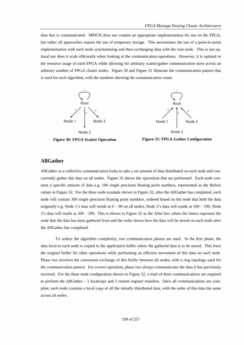
FPGA Message Passing Cluster Architectures
109 of 257
data that is communicated. MPICH does not contain an appropriate implementation for use on the FPGA,
but rather all approaches require the use of temporary storage. This necessitates the use of a point-to-point
implementation with each node synchronising and then exchanging data with the root node. This is not op-
timal nor does it scale efficiently when looking at the communication operations. However, it is optimal in
the resource usage of each FPGA while allowing for arbitrary scatter/gather communication sizes across an
arbitrary number of FPGA cluster nodes. Figure 30 and Figure 31 illustrate the communication pattern that
is used for each algorithm, with the numbers showing the communication count.
Root
Node 1
Node 2
Node 3
2
34
1
Figure 30: FPGA Scatter Operation
Root
Node 1
Node 2
Node 3
2
34
1
Figure 31: FPGA Gather Configuration
AllGather
AllGather as a collective communication looks to take a set amount of data distributed on each node and con-
currently gather this data on all nodes. Figure 32 shows the operations that are performed. Each node con-
tains a specific amount of data e.g. 100 single precision floating point numbers, represented as the Before
values in Figure 32. For the three node example shown in Figure 32, after the AllGather has completed, each
node will contain 300 single precision floating point numbers, ordered based on the node that held the data
originally e.g. Node 1’s data will reside at 0 – 99 on all nodes, Node 2’s data will reside at 100 – 199, Node
3’s data will reside at 200 – 299. This is shown in Figure 32 as the After box where the letters represent the
node that the data has been gathered from and the order shows how the data will be stored on each node after
the AllGather has completed.
To reduce the algorithm complexity, two communication phases are used. In the first phase, the
data local to each node is copied to the application buffer where the gathered data is to be stored. This frees
the original buffer for other operations while performing an efficient movement of this data on each node.
Phase two involves the concurrent exchange of this buffer between all nodes, with a ring topology used for
the communication pattern. For correct operation, phase two always communicates the data it has previously
received. For the three node configuration shown in Figure 32, a total of three communications are required
to perform the AllGather – 1 localcopy and 2 remote register transfers. Once all communications are com-
plete, each node contains a local copy of all the initially distributed data, with the order of this data the same
across all nodes.
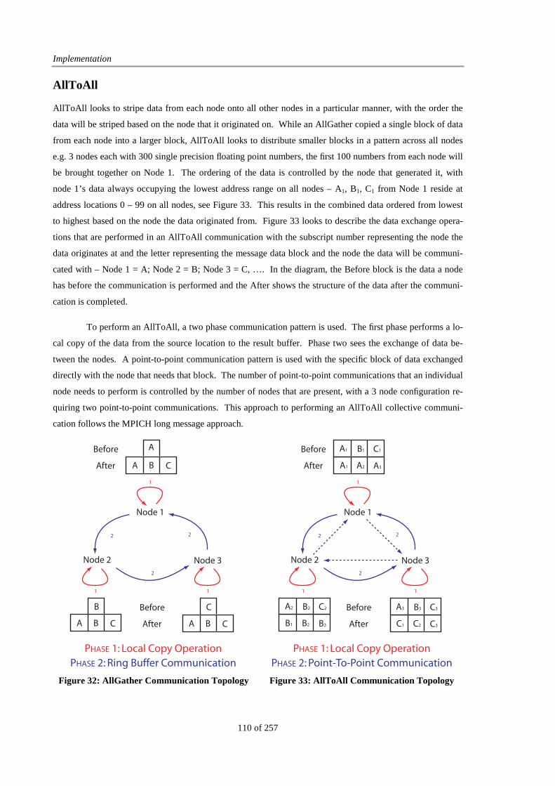
Implementation
110 of 257
AllToAll
AllToAll looks to stripe data from each node onto all other nodes in a particular manner, with the order the
data will be striped based on the node that it originated on. While an AllGather copied a single block of data
from each node into a larger block, AllToAll looks to distribute smaller blocks in a pattern across all nodes
e.g. 3 nodes each with 300 single precision floating point numbers, the first 100 numbers from each node will
be brought together on Node 1. The ordering of the data is controlled by the node that generated it, with
node 1’s data always occupying the lowest address range on all nodes – A1, B1, C1 from Node 1 reside at
address locations 0 – 99 on all nodes, see Figure 33. This results in the combined data ordered from lowest
to highest based on the node the data originated from. Figure 33 looks to describe the data exchange opera-
tions that are performed in an AllToAll communication with the subscript number representing the node the
data originates at and the letter representing the message data block and the node the data will be communi-
cated with – Node 1 = A; Node 2 = B; Node 3 = C, …. In the diagram, the Before block is the data a node
has before the communication is performed and the After shows the structure of the data after the communi-
cation is completed.
To perform an AllToAll, a two phase communication pattern is used. The first phase performs a lo-
cal copy of the data from the source location to the result buffer. Phase two sees the exchange of data be-
tween the nodes. A point-to-point communication pattern is used with the specific block of data exchanged
directly with the node that needs that block. The number of point-to-point communications that an individual
node needs to perform is controlled by the number of nodes that are present, with a 3 node configuration re-
quiring two point-to-point communications. This approach to performing an AllToAll collective communi-
cation follows the MPICH long message approach.
Node 1
Node 2 Node 3
1
11
2
2
2
Before
After A B C
Before
After
C
A B C
B
A B C
A
PHASE 1: Local Copy Operation
PHASE 2: Ring Buffer Communication
Figure 32: AllGather Communication Topology
Node 1
Node 2 Node 3
1
11
2
2
2
Before
After
A1 B1 C1
A1 A2 A3
Before
After
A3 B3 C3
C1 C2 C3
A2 B2 C2
B1 B2 B3
PHASE 1: Local Copy Operation
PHASE 2: Point-To-Point Communication
Figure 33: AllToAll Communication Topology

FPGA Message Passing Cluster Architectures
111 of 257
Collective Communication Limitation
During testing and development, a number of limitations were identified for both the implementations and the
overall operations of the message passing systems, in particular the hardware system. For the correct opera-
tion of the collective communications, a local copy operation is used, which copies data between memories
on the same node. The local copy operation needs to be supported regardless of the approach that is taken –
hardware, software – and is used to reduce the overheads that are required when moving data internally on
the node. This operation was not envisaged as part of the overall implementation and it is not directly or eas-
ily implementable within the system. This requires the use of the network to perform a localcopy operation.
This approach is non-optimal and increases operational overhead.
4.1.2 Point-to-Point Communication
The HDL MP API interface provides direct access to the point-to-point remote register transfer operations
that a distributed hardware application will use to exchange data. The physical point-to-point implementa-
tions are specific to both the hardware and FPGA processor solutions ensuring efficient operations however,
the following modes are possible based on the message passing communication command.
Ready Mode: Communications occur without requiring synchronisation. For a receive, the receive struc-
tures are configured immediately while for a send, the data is transmitted as soon as is possible regard-
less of whether the receiving node is active or able to buffer the messages.
Rendezvous Mode: Communication occurs after node synchronisation has been performed. In this configu-
ration, additional overheads exist for the synchronisation operations but overall performance stability is
improved from the synchronisation having occurred.
Buffered Mode: Communications follow the rendezvous mode of operation with the restriction that the mes-
sage data is located in an application register. This is in keeping with the idea that buffered data will be
data that has been read in and buffered as part of the application microarchitecture before performing
communications.
The operation of the different point-to-point communications is controlled by the communication
command interface, with a single communication performed at a time. Although the command interface only
supports a single communication at a time, the send and receive operations function independently allowing
for Send_Recv operations. This is illustrated in Figure 34 where the interface signals are assigned to the
communication control logic that will perform the communication operations. As shown, these units are dis-
tinct entities which operate independently of each other. This is used in the collective communications for
nodes that both send and receive data concurrently.
All collective communications use the rendezvous mode of communication to ensure stability of the
communication and also to enforce node synchronisation, ensuring all nodes perform the same collective
communication. All point-to-point register transfer operations are sender driven which means the node syn-
chronisation operations do not start until the sending node has initiated a remote register transmit operation.
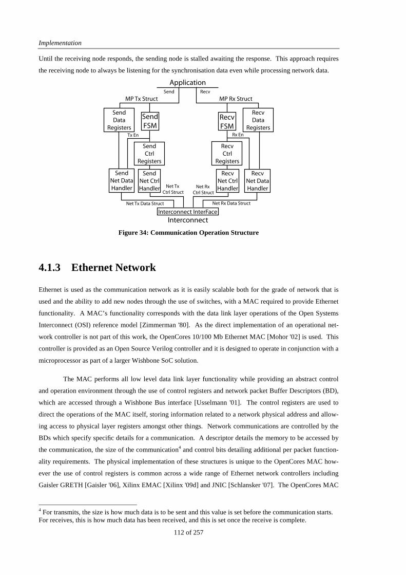
Implementation
112 of 257
Until the receiving node responds, the sending node is stalled awaiting the response. This approach requires
the receiving node to always be listening for the synchronisation data even while processing network data.
ApplicationSend Recv
SendFSM
RecvFSM
MP Tx Struct MP Rx Struct
SendCtrl
Registers
RecvCtrl
Registers
SendNet CtrlHandler
RecvNet CtrlHandler
SendData
Registers
SendNet DataHandler
RecvNet DataHandler
RecvData
Registers
Interconnect InterFace
Interconnect
Net Tx Data Struct
Net Tx Ctrl Struct
Net Rx Ctrl Struct
Net Rx Data Struct
Tx En Rx En
Figure 34: Communication Operation Structure
4.1.3 Ethernet Network
Ethernet is used as the communication network as it is easily scalable both for the grade of network that is
used and the ability to add new nodes through the use of switches, with a MAC required to provide Ethernet
functionality. A MAC’s functionality corresponds with the data link layer operations of the Open Systems
Interconnect (OSI) reference model [Zimmerman '80]. As the direct implementation of an operational net-
work controller is not part of this work, the OpenCores 10/100 Mb Ethernet MAC [Mohor '02] is used. This
controller is provided as an Open Source Verilog controller and it is designed to operate in conjunction with a
microprocessor as part of a larger Wishbone SoC solution.
The MAC performs all low level data link layer functionality while providing an abstract control
and operation environment through the use of control registers and network packet Buffer Descriptors (BD),
which are accessed through a Wishbone Bus interface [Usselmann '01]. The control registers are used to
direct the operations of the MAC itself, storing information related to a network physical address and allow-
ing access to physical layer registers amongst other things. Network communications are controlled by the
BDs which specify specific details for a communication. A descriptor details the memory to be accessed by
the communication, the size of the communication4 and control bits detailing additional per packet function-
ality requirements. The physical implementation of these structures is unique to the OpenCores MAC how-
ever the use of control registers is common across a wide range of Ethernet network controllers including
Gaisler GRETH [Gaisler '06], Xilinx EMAC [Xilinx '09d] and JNIC [Schlansker '07]. The OpenCores MAC
4 For transmits, the size is how much data is to be sent and this value is set before the communication starts. For receives, this is how much data has been received, and this is set once the receive is complete.

FPGA Message Passing Cluster Architectures
113 of 257
uses DMA operations to move communication data between application buffers and the network. The DMA
operations of the OpenCores MAC are able to read data from any address which is supplied and read from
the BDs.
The OpenCores MAC provides the operations necessary to implement a 10/100 Mb Ethernet net-
work. During the implementation of this work the value of using a Gigabit network for experiments became
apparent. This required an update of the controller to provide this functionality. The availability of the HDL
code and the on-FPGA implementation allowed this update to be performed. Operational fixes have also
been applied to meet the specific requirements of the dedicated hardware microarchitecture and the software
FPGA processor solutions. The following section looks at the modifications that are common to both ap-
proaches, before more details on the implementation optimisations for each approach are presented.
4.1.4 Gigabit Configuration Upgrade
To enable a larger range of tests and experiments, the OpenCores Ethernet MAC has been updated to support
Gigabit Ethernet operations while maintaining 10/100 Mb compatibility. This was required as the original
version was only 10/100 Mb compatible. The Wishbone Bus interface operations have been maintained and
expanded for correct Gigabit operations, removing the need to modify the message passing operations based
on the interconnect that is used. To maintain the same interface logic between message passing structures
and the MAC control registers, all updates and modifications to the controller are performed in the receive
and transmit control paths, shown in Figure 35. The structure of the controller is broken into three domains,
corresponding to different clock domains, the transmit domain and receive domain collectively referred to as
the communication domain and the operation and control domain which provides the interface for user opera-
tions, illustrated in Figure 35.
MII to GMII Update
10/100 Mb Ethernet interfaces with the physical network medium through the MII which defines control sig-
nals and datapath signals. These signals are specified by IEEE 802.3 [IEEE '05] and allow any MAC to use
any Physical layer chip once the MII signalling is correctly supported. For 10/100 Ethernet, the datapath
signals are 4 bits wide. For Gigabit Ethernet, an 8 bit datapath is used with an additional gigabit transmit
clock present. This updated interface is known as the Gigabit MII (GMII) and for gigabit operations must be
supported by both the MAC and the physical layer.

Implementation
114 of 257
User Clk
WishboneInterface Control
Logic
GMII / MII Interface
ReceiveInterface
TransmitInterface
ReceiveControl
TransmitControl
ReceiveData
TransmitData
ReceiveBuffer
TransmitBuffer
ControlRegisters
PacketBuffer
Descriptors
BufferControl
Logic
Flow
Control
Logic
Packet Type
Identification
and Removal
Additional
Registers
Packet
Insertion
and Creation
Inline
Packet
Creation
Rx Clk Tx Clk
Moved To
Cross Clock BRAM
Operation and Control Domain
Transmit DomainReceive Domain
Wishbone Interface
Figure 35: MAC Update Configuration detailing specific updates which have been applied to the
different operational units of the MAC controller. Updates presented along the outside include
updates present for the hardware only configuration.
Support for both the GMII and MII interfaces is provided at the lowest level. Selection of which in-
terface to use is based on the network the controller is connected to. To select the interface, the Physical
layer must be tested and the GMII/MII interface selected accordingly. To support the use of both interfaces,
an additional control register specifying which interface to use has been added. This register bit controls the
operations of the transmit and receive network state machines as well as the communication clock to be used.
The MII clock signals operate at 25 MHz, while GMII operates at 125 MHz. For the GMII interface, the
gigabit clock is generated by on-FPGA DCM modules. For a gigabit network, the 125 MHz clock is used to
drive all communication logic while if MII operations are used, the 25 MHz clock of the MII is used by the
same control logic. Interface selection requires the reading of physical layer registers to know which net-
work is being used. Based on the values from these registers, the interface selection register of the MAC is
set accordingly.
FIFO Buffer Modification
FIFO buffers are used to temporarily store communication data between system memory and the network.
These have been updated to support cross clock domain operations with the implementation presented by
Cummings and Alfke [Cummings '02] used. The buffer memory uses dual port Block RAMs as they support
cross clock domain operations natively. Block RAMs perform the cross clock domain operations of vector
data, while standard cross clock domain operations are used for the FIFO control signals. The use of these
FIFOs abstracts the interconnect communication operations from the control and interface logic.

FPGA Message Passing Cluster Architectures
115 of 257
Receive Buffer Descriptor
When data is received by the MAC, the BDs are checked to know if and where this data can be stored. To
support this, the next active receive BD is read during the receive Ethernet packet preamble. For 10/100 Mb
operations, the time overheads of this did not pose a problem. When moved to Gigabit Ethernet and the
GMII interface, the access overheads of the original controller created a race condition on reading back the
data. To remove this, the receive BD access pattern was modified. Rather than reading the BD data one at a
time, the access pattern was modified to using a burst read operation of all necessary data. To support this,
the BD memory has been split into two access interfaces, one for the Receive BD access from the network
logic, and one which supports access from the Wishbone and interface logic. The BDs are implemented us-
ing dual port Block RAMs to ensure independent operation of the receive BD accesses and the Wishbone
interface accesses.
CRC Modification
CRC is used by Ethernet to test and check that received data is correct and that no bit errors have occurred.
The transmitting node appends a 32-bit CRC to each packet, with the CRC generated for all data up to a
maximum size of 1514 bytes. Once the CRC is appended, the maximum packet size of 1518 bytes is gener-
ated. On the receiving node, all network data including the CRC passes through the CRC generation logic.
If no errors have been generated, the resulting CRC will match the magic 32-bit CRC value, regardless of the
data or the transmit generated CRC that has been appended. The original MAC uses 4-bit CRC arithmetic.
To support both MII and GMII interfaces, the CRC logic has been updated to use 8-bit arithmetic with a con-
version required between the 4-bit MII signals and the 8-bit CRC logic. The interface selection control bit
selects if additional operations need to be performed on the receive data i.e. converting 4-bit data into 8-bit
data by concatenating two 4-bit blocks together. The implementation of the 8-bit CRC unit assumes that all
communications will be byte aligned.
Gigabit Controller Modification Limitations
The controller updates meet experiment requirements of allowing FPGAs to communicate and operate cor-
rectly on a Gigabit Ethernet network. The updates have been extensively tested but some operational limita-
tions exist, with a lack of Jumbo packet support a drawback. Jumbo packets are an extension of the IEEE
802.3 standard where larger than normal packets can be communicated, up to 9,000 bytes. The use of larger
packets reduce the cost of generating and processing packets, allowing for reduced overheads and improved
throughput by an Ethernet network end point. Jumbo packets use was not seen as necessary for the experi-
ments and this functionality has not been provided. From the registers and operations of the OpenCores con-
troller, the addition of Jumbo packet support should not be difficult. Cross clock domain tests show that all
operations work correctly between a 100 MHz user clock and the required 125 MHz network clock. As 100
MHz is the targeted application speed, further testing of the cross clock logic was not undertaken.

Implementation
116 of 257
4.1.5 Packet Control Operations Update
Packets that are received by the network controller have to be transferred between the FIFO buffers and the
hardware application microarchitecture register memories. While implementing the design, certain deficien-
cies were identified with these data movement operations. Updates that address these deficiencies are pre-
sented here and relate to packet operations that are common for both the hardware and FPGA processor net-
work operations.
Transmission Watermark
When performing a transmission, data is read from application memory into the FIFO buffers before it is
communicated. The buffers are used to ensure stable communications occur and as such, a transmit buffer
should not become empty (underrun) before all data has been transmitted. When testing the controller with
high latency memory, transmission underruns occurred frequently. A number of solutions were investigated
to resolve this including complete packet buffering before transmission. As efficiency is required for both
10/100 Mb Ethernet and Gigabit Ethernet, and with the ability to read data concurrently to communication
operations, a complete copy operation was ruled out as introducing too much overhead through reduced net-
work bandwidth performance. This copy operation is distinct and different to packet buffering where the
communication data for a following transmission is read and stored in advance of that communication.
A transmit buffer watermark is implemented to allow for efficient communication with the amount
of data buffered depending on the communication size. For different packet sizes, different amounts of data
would be read in before triggering the transmit operations. By using different values, different sized commu-
nications are able to operate correctly and efficiently. Concurrent reading of the remaining data is performed
while the communication is ongoing. The use of the transmission watermark stabilises communications
when external high latency memory is storing the remote register transfer data.
Memory Aligned DMA Operations
The OpenCores controller uses DMA to read and write data directly from the network to application specified
memory, based on the data address supplied by the communication BDs. When the controller performs the
DMA operation, it starts at the base address and burst transfers the data between the network buffers and the
application memory. This burst transfer however does not take into account memory hierarchies or imple-
mentation architectures. This means it burst accesses the data it requires regardless of whether more efficient
approaches are possible. This architecture proved inefficient when accessing external memory where data
aligned accesses are enforced. Non-aligned accesses will be inefficient as different memory banks need to be
charged and otherwise updated to support the extra access. The DMA operations of the interface logic have
been updated to use 32-byte aligned memory reads while supporting shorter bursts up to a 32-byte alignment
as required. This architecture supports better memory accesses when interfacing the control logic with exter-
nal DDR memory.
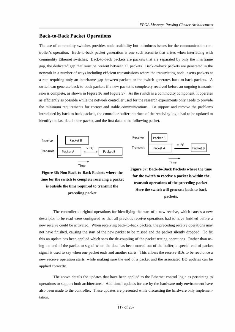
FPGA Message Passing Cluster Architectures
117 of 257
Back-to-Back Packet Operations
The use of commodity switches provides node scalability but introduces issues for the communication con-
troller’s operation. Back-to-back packet generation is one such scenario that arises when interfacing with
commodity Ethernet switches. Back-to-back packets are packets that are separated by only the interframe
gap, the dedicated gap that must be present between all packets. Back-to-back packets are generated in the
network in a number of ways including efficient transmissions where the transmitting node inserts packets at
a rate requiring only an interframe gap between packets or the switch generates back-to-back packets. A
switch can generate back-to-back packets if a new packet is completely received before an ongoing transmis-
sion is complete, as shown in Figure 36 and Figure 37. As the switch is a commodity component, it operates
as efficiently as possible while the network controller used for the research experiments only needs to provide
the minimum requirements for correct and stable communications. To support and remove the problems
introduced by back to back packets, the controller buffer interface of the receiving logic had to be updated to
identify the last data in one packet, and the first data in the following packet.
Receive
Transmit Packet A> IFG
Time
Packet B
Packet B
Figure 36: Non Back-to-Back Packets where the
time for the switch to complete receiving a packet
is outside the time required to transmit the
preceding packet
Receive
Transmit Packet A
Packet B
= IFGPacket B
Time
Figure 37: Back-to-Back Packets where the time
for the switch to receive a packet is within the
transmit operations of the preceding packet.
Here the switch will generate back to back
packets.
The controller’s original operations for identifying the start of a new receive, which causes a new
descriptor to be read were configured so that all previous receive operations had to have finished before a
new receive could be activated. When receiving back-to-back packets, the preceding receive operations may
not have finished, causing the start of the new packet to be missed and the packet silently dropped. To fix
this an update has been applied which sees the de-coupling of the packet testing operations. Rather than us-
ing the end of the packet to signal when the data has been moved out of the buffer, a special end-of-packet
signal is used to say when one packet ends and another starts. This allows the receive BDs to be read once a
new receive operation starts, while making sure the end of a packet and the associated BD updates can be
applied correctly.
The above details the updates that have been applied to the Ethernet control logic as pertaining to
operations to support both architectures. Additional updates for use by the hardware only environment have
also been made to the controller. These updates are presented while discussing the hardware only implemen-
tation.
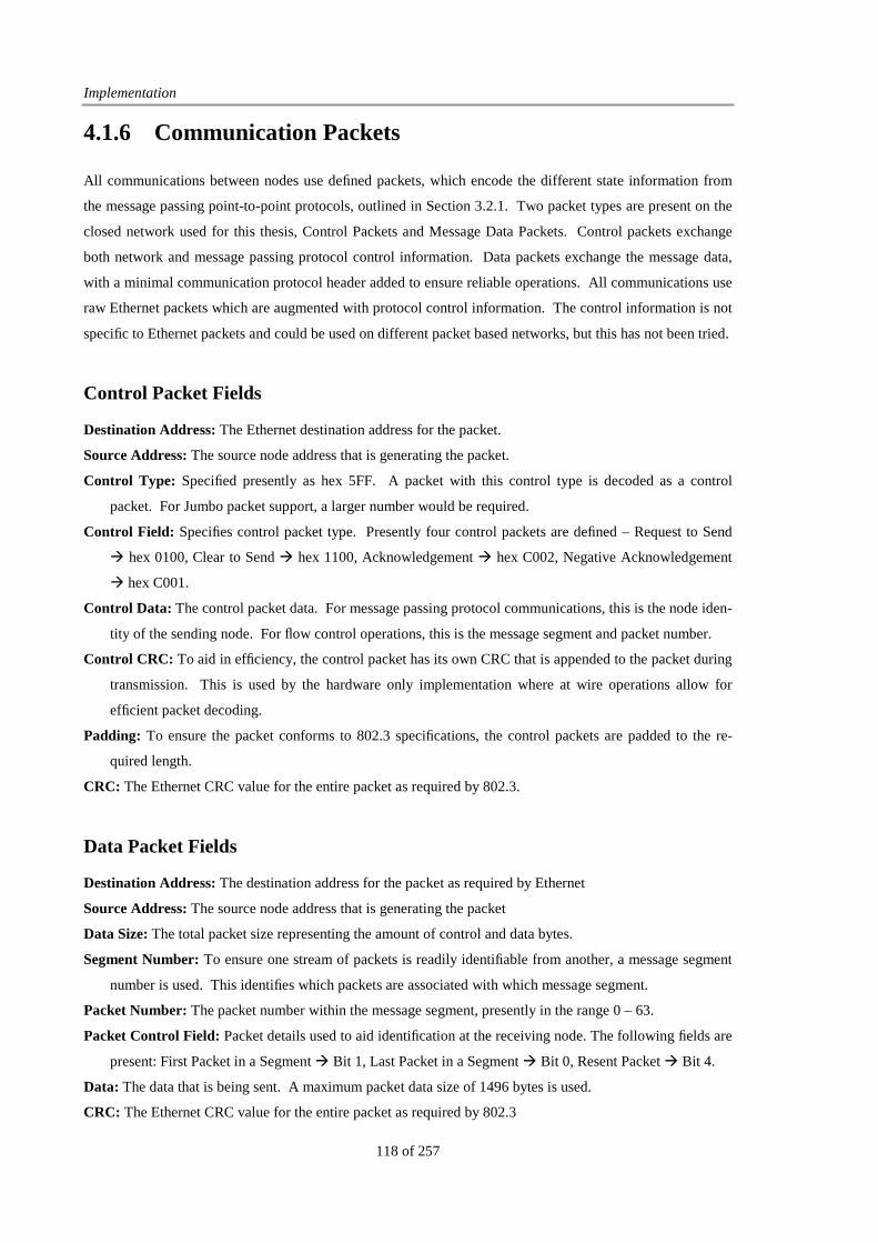
Implementation
118 of 257
4.1.6 Communication Packets
All communications between nodes use defined packets, which encode the different state information from
the message passing point-to-point protocols, outlined in Section 3.2.1. Two packet types are present on the
closed network used for this thesis, Control Packets and Message Data Packets. Control packets exchange
both network and message passing protocol control information. Data packets exchange the message data,
with a minimal communication protocol header added to ensure reliable operations. All communications use
raw Ethernet packets which are augmented with protocol control information. The control information is not
specific to Ethernet packets and could be used on different packet based networks, but this has not been tried.
Control Packet Fields
Destination Address: The Ethernet destination address for the packet.
Source Address: The source node address that is generating the packet.
Control Type: Specified presently as hex 5FF. A packet with this control type is decoded as a control
packet. For Jumbo packet support, a larger number would be required.
Control Field: Specifies control packet type. Presently four control packets are defined – Request to Send
� hex 0100, Clear to Send � hex 1100, Acknowledgement � hex C002, Negative Acknowledgement
� hex C001.
Control Data: The control packet data. For message passing protocol communications, this is the node iden-
tity of the sending node. For flow control operations, this is the message segment and packet number.
Control CRC: To aid in efficiency, the control packet has its own CRC that is appended to the packet during
transmission. This is used by the hardware only implementation where at wire operations allow for
efficient packet decoding.
Padding: To ensure the packet conforms to 802.3 specifications, the control packets are padded to the re-
quired length.
CRC: The Ethernet CRC value for the entire packet as required by 802.3.
Data Packet Fields
Destination Address: The destination address for the packet as required by Ethernet
Source Address: The source node address that is generating the packet
Data Size: The total packet size representing the amount of control and data bytes.
Segment Number: To ensure one stream of packets is readily identifiable from another, a message segment
number is used. This identifies which packets are associated with which message segment.
Packet Number: The packet number within the message segment, presently in the range 0 – 63.
Packet Control Field: Packet details used to aid identification at the receiving node. The following fields are
present: First Packet in a Segment � Bit 1, Last Packet in a Segment � Bit 0, Resent Packet � Bit 4.
Data: The data that is being sent. A maximum packet data size of 1496 bytes is used.
CRC: The Ethernet CRC value for the entire packet as required by 802.3
FPGA Message Passing Cluster Architectures
119 of 257
Destination Address 6 Bytes Destination Address 6 Bytes
Source Address 6 Bytes Source Address 6 Bytes
Control Type 2 Bytes Data Size 2 Bytes
Control Field 2 Bytes Segment Number 1 Byte
Control Data 2 Bytes Packet Number 1 Byte
Control CRC5 4 Bytes Packet Control Field 1 Byte
Padding 38 Bytes Data 43 - 1496 Bytes
CRC 4 Bytes CRC 4 Bytes
Control Packet Configuration Message Data Packet Configuration
Control Packet Operations
Control packets can be received at a node at any time though unexpected receive message data packets will
be dropped even though ready mode communications are possible. A node is able to generate message pass-
ing control packets asynchronously to the operations of other nodes meaning a node can receive a control
packet before it expects one. The unexpected receive operations that a node supports are unique to the two
evaluation approaches. However, the operations performed on the control packet data are consistent between
each approach.
A message passing control packet, identifying the state in the message passing protocol, is received
and decoded as part of the low level network operations. The low level network does not have knowledge of
how a higher layer protocol operates, though it is aware of how to decode the control packet. Once a mes-
sage passing control packet has been identified, the node identity is decoded and this number passed to the
message passing protocol. To remove a costly translate operation, between the Ethernet MAC address and
the message passing identity, the message passing identity of the sending node is exchanged within the net-
work packet. This does not increase the communication overhead of the control packet as padding is still
required to meet the minimum packet length of Ethernet. As message passing control packets can be re-
ceived at any time, the information contained in the packet may not be used immediately. Rather, the exis-
tence of this packet is stored and acted upon by a future message passing communication. The exact details
of how this is stored are implementation specific, with the hardware only solution storing data in a dedicated
Block RAM, while the software stores the details in a data array.
Network flow control packets are used by the communication protocol to ensure the correct ex-
change of message data between nodes. The operation of these control packets has been presented previ-
ously in Section 3.2.2. The control data within a network flow control packet details which packet has been
correctly accepted. If an acknowledgement packet is received, this data can be ignored as the segment has
5 Hardware only. Not present for software implementation as costly to implement and differences between hardware and software systems make this redundant for the software system.
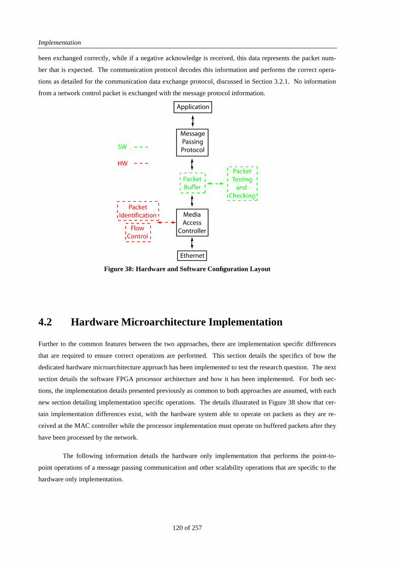
Implementation
120 of 257
been exchanged correctly, while if a negative acknowledge is received, this data represents the packet num-
ber that is expected. The communication protocol decodes this information and performs the correct opera-
tions as detailed for the communication data exchange protocol, discussed in Section 3.2.1. No information
from a network control packet is exchanged with the message protocol information.
Ethernet
MediaAccess
ControllerFlowControl
PacketIdentification
PacketBuffer
PacketTesting
and Checking
Application
MessagePassingProtocolSW
HW
Figure 38: Hardware and Software Configuration Layout
4.2 Hardware Microarchitecture Implementation
Further to the common features between the two approaches, there are implementation specific differences
that are required to ensure correct operations are performed. This section details the specifics of how the
dedicated hardware microarchitecture approach has been implemented to test the research question. The next
section details the software FPGA processor architecture and how it has been implemented. For both sec-
tions, the implementation details presented previously as common to both approaches are assumed, with each
new section detailing implementation specific operations. The details illustrated in Figure 38 show that cer-
tain implementation differences exist, with the hardware system able to operate on packets as they are re-
ceived at the MAC controller while the processor implementation must operate on buffered packets after they
have been processed by the network.
The following information details the hardware only implementation that performs the point-to-
point operations of a message passing communication and other scalability operations that are specific to the
hardware only implementation.

FPGA Message Passing Cluster Architectures
121 of 257
4.2.1 Architecture
The architecture of the dedicated hardware microarchitecture is bro-
ken into three layers, the message passing operations which store
message passing protocol information, network specific operations
which configure the network control structures based on the message
passing protocol operations and finally, the network flow control
operations which ensure the correct and reliable exchange of mes-
sage passing data between nodes. Figure 39 illustrates the first two
operations that are performed, with the operations of each layer bro-
ken into more defined operations. The flow control operations are
performed in the Ethernet controller as additional control signals and
will be detailed in Section 4.2.3. Figure 40 illustrates the control
signal configuration for the message passing specific operations
while Figure 44 illustrates the network control hardware which the
message passing system controls to perform communication opera-
tions.
Message Passing State Machines
The point-to-point message passing protocols (send and receive)
presented in Chapter 3 have been implemented as two dedicated hardware state machines, one each for re-
ceive and transmit. The state machines have been implemented and tested using blocking communications.
From previously presented details, Section 3.1.1, the message passing state machines accept the HDL MP
API communication interface requests and control the network specific structures to perform the hardware
application remote register transfer operations using message passing principles. For rendezvous mode
communications, this requires the operation of the synchronisation packet generation while with ready mode
communications, the state machines must initiate the data communication operation directly.
The state machines as implemented are used to control the network’s operations, with the network
DMA unit performing the data movement operations, providing a zero copy approach. To support a zero
copy approach, all connected memory must be accessible to the network controller, with the on-FPGA inter-
connect providing a memory mapped scheme that allows DMA accesses to both external memory and appli-
cation specific registers. To perform the message passing communication, a data address pointer must be
explicitly provided which defines the base address for the data, with defined addresses used for both external
memory, starting at hex 0, and application specific buffers, starting at address hex 80000000. Message com-
munication size is also required which the lower layer implementation specific control hardware uses to con-
figure the network control registers and BDs. The node identity is used to select the destination network spe-
cific address from the network address list and the MAC address is passed to the lower layer control hard-
ware where it is configured to perform inline packetisation operations.
MP ProtocolOperations
MP ProtocolOperations
HDL MP API
Rx QueueTx Queue
SendFragmentation
ReceiveFragmentation
SendFSM
TransmitBuffer
Descriptors
ReceiveFSM
ReceiveBuffer
Descriptors
Network
On-FPGA Interconnect Logic
Figure 39: Communication Control
Configuration
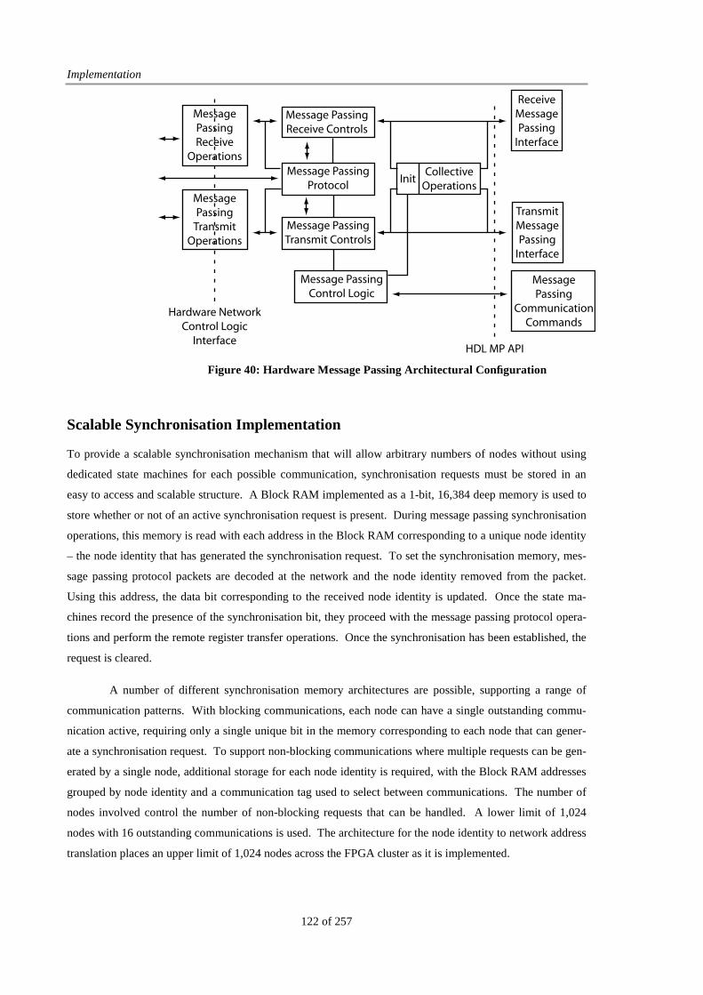
Implementation
122 of 257
Scalable Synchronisation Implementation
To provide a scalable synchronisation mechanism that will allow arbitrary numbers of nodes without using
dedicated state machines for each possible communication, synchronisation requests must be stored in an
easy to access and scalable structure. A Block RAM implemented as a 1-bit, 16,384 deep memory is used to
store whether or not of an active synchronisation request is present. During message passing synchronisation
operations, this memory is read with each address in the Block RAM corresponding to a unique node identity
– the node identity that has generated the synchronisation request. To set the synchronisation memory, mes-
sage passing protocol packets are decoded at the network and the node identity removed from the packet.
Using this address, the data bit corresponding to the received node identity is updated. Once the state ma-
chines record the presence of the synchronisation bit, they proceed with the message passing protocol opera-
tions and perform the remote register transfer operations. Once the synchronisation has been established, the
request is cleared.
A number of different synchronisation memory architectures are possible, supporting a range of
communication patterns. With blocking communications, each node can have a single outstanding commu-
nication active, requiring only a single unique bit in the memory corresponding to each node that can gener-
ate a synchronisation request. To support non-blocking communications where multiple requests can be gen-
erated by a single node, additional storage for each node identity is required, with the Block RAM addresses
grouped by node identity and a communication tag used to select between communications. The number of
nodes involved control the number of non-blocking requests that can be handled. A lower limit of 1,024
nodes with 16 outstanding communications is used. The architecture for the node identity to network address
translation places an upper limit of 1,024 nodes across the FPGA cluster as it is implemented.
MessagePassingReceive
Operations
MessagePassing
TransmitOperations
Message PassingReceive Controls
Message PassingTransmit Controls
Message PassingProtocol
InitCollective
Operations
Message PassingControl Logic
ReceiveMessagePassing
Interface
TransmitMessagePassing
Interface
MessagePassing
CommunicationCommands
HDL MP API
Hardware NetworkControl Logic
Interface
Figure 40: Hardware Message Passing Architectural Configuration
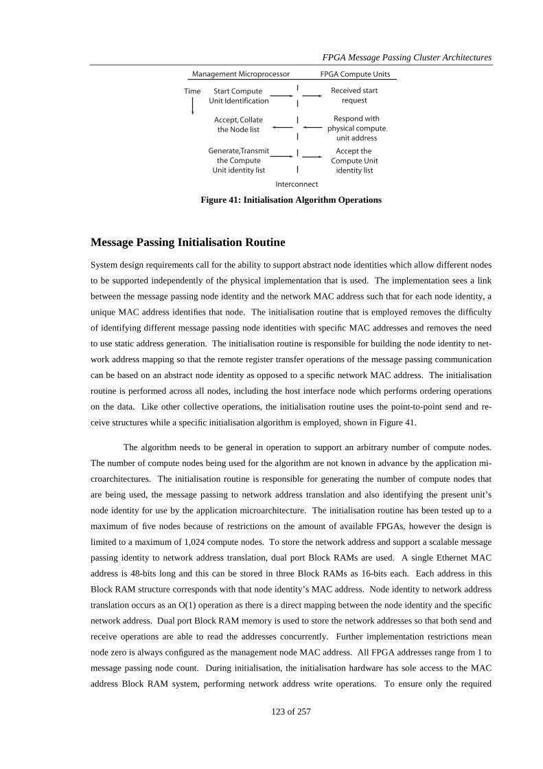
FPGA Message Passing Cluster Architectures
123 of 257
Message Passing Initialisation Routine
System design requirements call for the ability to support abstract node identities which allow different nodes
to be supported independently of the physical implementation that is used. The implementation sees a link
between the message passing node identity and the network MAC address such that for each node identity, a
unique MAC address identifies that node. The initialisation routine that is employed removes the difficulty
of identifying different message passing node identities with specific MAC addresses and removes the need
to use static address generation. The initialisation routine is responsible for building the node identity to net-
work address mapping so that the remote register transfer operations of the message passing communication
can be based on an abstract node identity as opposed to a specific network MAC address. The initialisation
routine is performed across all nodes, including the host interface node which performs ordering operations
on the data. Like other collective operations, the initialisation routine uses the point-to-point send and re-
ceive structures while a specific initialisation algorithm is employed, shown in Figure 41.
The algorithm needs to be general in operation to support an arbitrary number of compute nodes.
The number of compute nodes being used for the algorithm are not known in advance by the application mi-
croarchitectures. The initialisation routine is responsible for generating the number of compute nodes that
are being used, the message passing to network address translation and also identifying the present unit’s
node identity for use by the application microarchitecture. The initialisation routine has been tested up to a
maximum of five nodes because of restrictions on the amount of available FPGAs, however the design is
limited to a maximum of 1,024 compute nodes. To store the network address and support a scalable message
passing identity to network address translation, dual port Block RAMs are used. A single Ethernet MAC
address is 48-bits long and this can be stored in three Block RAMs as 16-bits each. Each address in this
Block RAM structure corresponds with that node identity’s MAC address. Node identity to network address
translation occurs as an O(1) operation as there is a direct mapping between the node identity and the specific
network address. Dual port Block RAM memory is used to store the network addresses so that both send and
receive operations are able to read the addresses concurrently. Further implementation restrictions mean
node zero is always configured as the management node MAC address. All FPGA addresses range from 1 to
message passing node count. During initialisation, the initialisation hardware has sole access to the MAC
address Block RAM system, performing network address write operations. To ensure only the required
Start Compute Unit Identification
Interconnect
Management Microprocessor FPGA Compute Units
Accept, Collatethe Node list
Generate,Transmitthe Compute
Unit identity list
Accept the Compute Unit
identity list
Received startrequest
Respond withphysical compute
unit address
Time
Figure 41: Initialisation Algorithm Operations
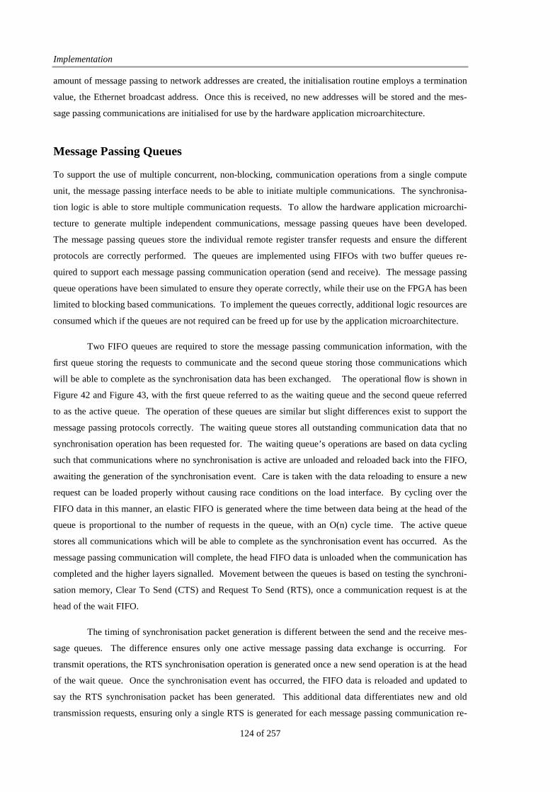
Implementation
124 of 257
amount of message passing to network addresses are created, the initialisation routine employs a termination
value, the Ethernet broadcast address. Once this is received, no new addresses will be stored and the mes-
sage passing communications are initialised for use by the hardware application microarchitecture.
Message Passing Queues
To support the use of multiple concurrent, non-blocking, communication operations from a single compute
unit, the message passing interface needs to be able to initiate multiple communications. The synchronisa-
tion logic is able to store multiple communication requests. To allow the hardware application microarchi-
tecture to generate multiple independent communications, message passing queues have been developed.
The message passing queues store the individual remote register transfer requests and ensure the different
protocols are correctly performed. The queues are implemented using FIFOs with two buffer queues re-
quired to support each message passing communication operation (send and receive). The message passing
queue operations have been simulated to ensure they operate correctly, while their use on the FPGA has been
limited to blocking based communications. To implement the queues correctly, additional logic resources are
consumed which if the queues are not required can be freed up for use by the application microarchitecture.
Two FIFO queues are required to store the message passing communication information, with the
first queue storing the requests to communicate and the second queue storing those communications which
will be able to complete as the synchronisation data has been exchanged. The operational flow is shown in
Figure 42 and Figure 43, with the first queue referred to as the waiting queue and the second queue referred
to as the active queue. The operation of these queues are similar but slight differences exist to support the
message passing protocols correctly. The waiting queue stores all outstanding communication data that no
synchronisation operation has been requested for. The waiting queue’s operations are based on data cycling
such that communications where no synchronisation is active are unloaded and reloaded back into the FIFO,
awaiting the generation of the synchronisation event. Care is taken with the data reloading to ensure a new
request can be loaded properly without causing race conditions on the load interface. By cycling over the
FIFO data in this manner, an elastic FIFO is generated where the time between data being at the head of the
queue is proportional to the number of requests in the queue, with an O(n) cycle time. The active queue
stores all communications which will be able to complete as the synchronisation event has occurred. As the
message passing communication will complete, the head FIFO data is unloaded when the communication has
completed and the higher layers signalled. Movement between the queues is based on testing the synchroni-
sation memory, Clear To Send (CTS) and Request To Send (RTS), once a communication request is at the
head of the wait FIFO.
The timing of synchronisation packet generation is different between the send and the receive mes-
sage queues. The difference ensures only one active message passing data exchange is occurring. For
transmit operations, the RTS synchronisation operation is generated once a new send operation is at the head
of the wait queue. Once the synchronisation event has occurred, the FIFO data is reloaded and updated to
say the RTS synchronisation packet has been generated. This additional data differentiates new and old
transmission requests, ensuring only a single RTS is generated for each message passing communication re-
FPGA Message Passing Cluster Architectures
125 of 257
quest. On the receiving node, once a synchronisation event has been received, the communication informa-
tion is loaded into the active queue. The receive system generates its CTS synchronisation packet once the
receive is at the head of the active queue. Generating the synchronisation event when it is at the head of the
queue ensures that when data is received it is for this message communication operation.
Fragmentation Operation
Arbitrary message sizes are supported at the HDL MP API requiring the implementation of fragmentation
logic which is used to break the message data into network specific sizes that can be exchanged between
communicating nodes. As shown in Figure 39, the fragmentation operations occur between the message
passing control logic and the network specific control logic which configures the network communication
registers. Data fragmentation operations are performed by specific hardware which use the algorithm de-
scribed in Section 3.2.4 and implement the computation operations. Data fragmentation is performed on both
sending and receiving nodes, with the sending node concerned with taking the large message data and split-
ting it, while on the receiving node the concern is how each packet is merged back to create the original mes-
sage. Two aspects are required for this, the generation of the packet size to be used for each part and the ad-
dress at which that packet starts. For efficient FPGA operations, an iterative approach is used with the start-
ing address of each packet, the sum of the size of all packets to that iteration, the upper limit based on the
subtraction of all data that has been configured and the amount of data to be sent with an additional register
used to determine when the amount of outstanding data would require only two packets. To determine when
the amount of data left to be communicated only requires two packets, a data comparison operation is used
which looks to compare the amount of outstanding data against both the maximum packet size that is sup-
ported and twice the maximum packet size. If the data is larger than the maximum packet size but not larger
than twice the packet size, the data requires two packets to communicate. Both comparisons are required and
can be efficiently performed in parallel. The developed fragmentation logic allows the maximum packet size
to be specified and by using the comparison configuration, just described, an arbitrary packet size between a
minimum and maximum can be used to generate the fragmentation requirements. This aspect was useful
during simulation testing where an artificially small packet size was used to reduce simulation times without
HDL MP APISEND INTERFACE
WAIT
FIFO
ACTIVE
FIFO
CTSBRAM
ACTIVE NET
SEND
ACTIVATE NET
REQUEST
CONTROL
STATE
MACHINE
Figure 42: Transmit Message Queue
HDL MP APIRECEIVE INTERFACE
WAIT
FIFO
ACTIVE
FIFO
RTSBRAM
ACTIVE NET
RECEIVE
ACTIVATE NET
RESPONSE
CONTROL
STATE
MACHINE
Figure 43: Receive Message Queue
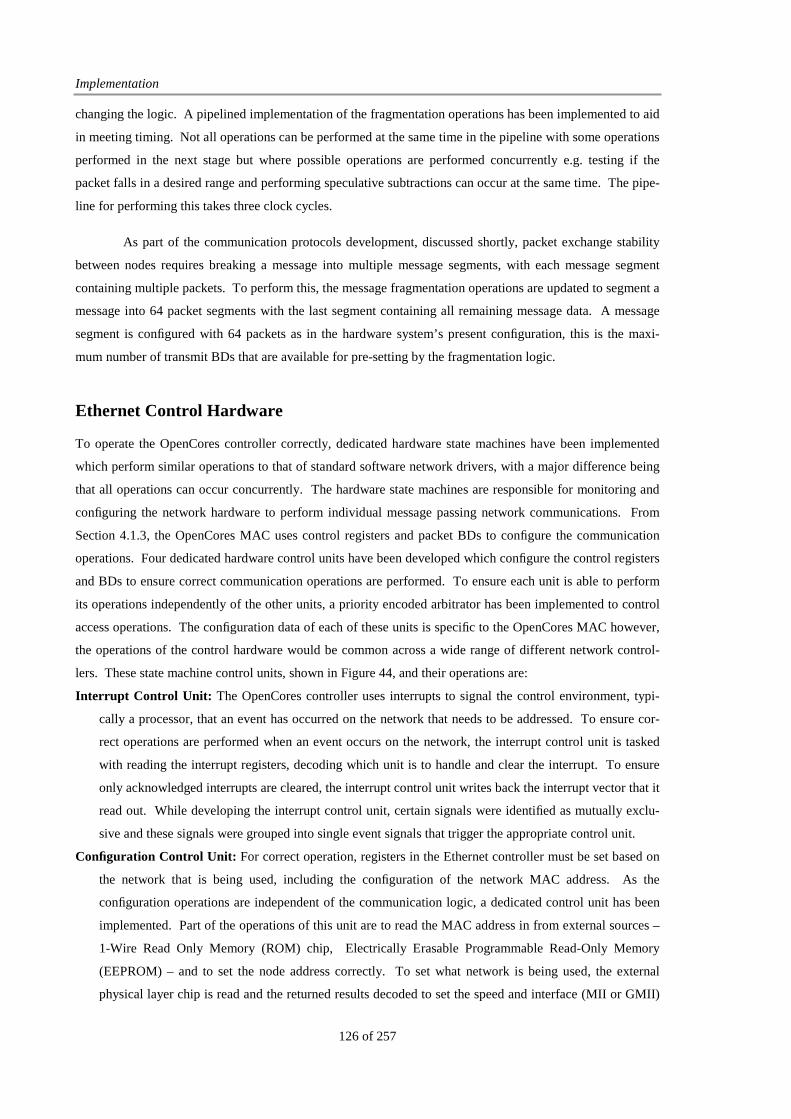
Implementation
126 of 257
changing the logic. A pipelined implementation of the fragmentation operations has been implemented to aid
in meeting timing. Not all operations can be performed at the same time in the pipeline with some operations
performed in the next stage but where possible operations are performed concurrently e.g. testing if the
packet falls in a desired range and performing speculative subtractions can occur at the same time. The pipe-
line for performing this takes three clock cycles.
As part of the communication protocols development, discussed shortly, packet exchange stability
between nodes requires breaking a message into multiple message segments, with each message segment
containing multiple packets. To perform this, the message fragmentation operations are updated to segment a
message into 64 packet segments with the last segment containing all remaining message data. A message
segment is configured with 64 packets as in the hardware system’s present configuration, this is the maxi-
mum number of transmit BDs that are available for pre-setting by the fragmentation logic.
Ethernet Control Hardware
To operate the OpenCores controller correctly, dedicated hardware state machines have been implemented
which perform similar operations to that of standard software network drivers, with a major difference being
that all operations can occur concurrently. The hardware state machines are responsible for monitoring and
configuring the network hardware to perform individual message passing network communications. From
Section 4.1.3, the OpenCores MAC uses control registers and packet BDs to configure the communication
operations. Four dedicated hardware control units have been developed which configure the control registers
and BDs to ensure correct communication operations are performed. To ensure each unit is able to perform
its operations independently of the other units, a priority encoded arbitrator has been implemented to control
access operations. The configuration data of each of these units is specific to the OpenCores MAC however,
the operations of the control hardware would be common across a wide range of different network control-
lers. These state machine control units, shown in Figure 44, and their operations are:
Interrupt Control Unit: The OpenCores controller uses interrupts to signal the control environment, typi-
cally a processor, that an event has occurred on the network that needs to be addressed. To ensure cor-
rect operations are performed when an event occurs on the network, the interrupt control unit is tasked
with reading the interrupt registers, decoding which unit is to handle and clear the interrupt. To ensure
only acknowledged interrupts are cleared, the interrupt control unit writes back the interrupt vector that it
read out. While developing the interrupt control unit, certain signals were identified as mutually exclu-
sive and these signals were grouped into single event signals that trigger the appropriate control unit.
Configuration Control Unit: For correct operation, registers in the Ethernet controller must be set based on
the network that is being used, including the configuration of the network MAC address. As the
configuration operations are independent of the communication logic, a dedicated control unit has been
implemented. Part of the operations of this unit are to read the MAC address in from external sources –
1-Wire Read Only Memory (ROM) chip, Electrically Erasable Programmable Read-Only Memory
(EEPROM) – and to set the node address correctly. To set what network is being used, the external
physical layer chip is read and the returned results decoded to set the speed and interface (MII or GMII)

FPGA Message Passing Cluster Architectures
127 of 257
to use for network communications. While developing the system operations, this unit was updated to
wipe the BD fields on a reset. Block RAM units maintain their data between resets requiring specific re-
set hardware which clears all BDs.
Receive Control Unit: To perform a communication, the individual receive BDs must be set, detailing the
specific operations for that individual communication. The BDs detail the specifics of each individual
communication with additional registers present for the hardware only configuration to allow at-wire
flow control packet testing and depacketisation operations. The receive control units main operations are
to configure where data is to be stored and how depacketisation is to be performed. As at-wire flow con-
trol is performed, this unit does not need to read back the size of the received packet. Development of
the receive control unit showed that the order registers are set is important to ensure race conditions do
not occur, such that all control information must be set before the BD is enabled to receive data.
Transmit Control Unit: Transmit BDs control the operations for performing a transmit operation including
configuring the destination MAC address to be communicated with and inline packetisation operations.
When configuring the transmit BDs, the register control information must be set before a transmit buffer
is enabled to ensure a race condition does not occur. Unlike the receive BDs, once a transmit BD has
been enabled, the MAC control hardware commences operations immediately, causing a high likelihood
of a race condition. The hardware only BDs have been augmented to include the destination MAC ad-
dress as well as other registers to allow for per packet inline at-wire packetisation operations.
A priority encoded arbitration unit has been developed which allows each control unit reliably ac-
cess the Ethernet control registers. As multiple units are attempting to access the same structures across an
interconnect bus, an arbitration unit is required, while the priority of efficient interrupt resolution necessitates
the use of a priority encoded arbitrator. The interrupt control unit has the highest priority, however, this con-
trol unit is called infrequently, in response to network events. The operation of the other control units is tied
to events that happen on the network and as such, a portion of their operations are based on event triggers
from the network. This makes it unlikely that the interrupt control unit will cause a delay in the other units
while it exercises its priority access. The configuration control unit has the next highest priority as apart from
network initialisation, it does not perform many ongoing operations on a node. The transmit and receive con-
trollers normally have equal priority, however, transmit operations have been configured with a higher prior-
ity to ensure that resources on the node can be freed through the transmission of network data. The receive
control unit has the lowest priority.
EthernetController Registers
PriorityArbitration
InterruptController
Rx Controller
Tx Controller
ConfigurationController
Message Passing Receive Operations
Message Passing Transmit Operations
InterruptVector
Figure 44: Hardware Control Logic Configuration

Implementation
128 of 257
4.2.2 Hardware On-FPGA Interconnect
For the hardware only configuration, an on-FPGA interconnect is used to provide access between the differ-
ent components that make up the dedicated hardware microarchitecture. The on-chip operations have been
implemented to use the Wishbone SoC as the OpenCores Ethernet MAC supports this. A SoC bus uses a
master/slave data exchange approach where masters start an access with slaves the target for the access, e.g.
memory reads. The OpenCores Ethernet MAC is implemented with a Master interface used by the DMA
control logic and a Slave interface which provides access to the network registers and BDs. The test envi-
ronment for the OpenCores MAC supplies a bus-based priority encoded SoC interconnect solution, with two
master interfaces and two slave interfaces, and this has been updated to provide the interconnect functionality
for the dedicated hardware microarchitecture. Details on this interconnect are specific to the Hardware only
configuration, while details on the Software only interconnect are provided in Section 4.3.1.
To meet the requirements for the hardware solution, a three master – four slave memory mapped
crossbar SoC has been implemented which uses priority burst accesses, shown in Figure 45. This solution
has been developed from the original two master – two slave interconnect supplied as part of the OpenCores
MAC test environment. The three masters are the Network DMA logic, the HDL MP API memory interface
and the Ethernet control logic. The four slaves are the Network registers and BDs, external memory, the
message passing synchronisation buffers and network connected hardware application microarchitecture
buffers of the HDL MP API.
Priority EncodedSelection Logic
EthernetControllerHardware
NetworkDMA Logic
HDL MP APIMemoryInterface
MemoryInterface
NetworkSlave Interface
Network ConnectedApplication Buffers
SynchronisationBuffer Interface
Figure 45: Crossbar Interconnect Structure
The interconnect has been implemented using priority based encoding with the following encoding,
from highest priority to lowest: Network DMA operations, HDL MP API memory interface, Ethernet control
hardware. This priority is based on criticality of access for each master. The network DMA logic has the
highest priority to ensure correct network operations so that network FIFOs do not enter an invalid state caus-
ing either transmit underruns or receive overflows. The Ethernet control hardware has the lowest priority as
it is only responsible for accessing the network control registers and this is not expected to occur as fre-

FPGA Message Passing Cluster Architectures
129 of 257
quently as other operations. The use of the crossbar interconnect mitigates against the impact of a priority
encoded arbitration scheme as once each master is accessing a different slave, no conflict will occur for ac-
cess and thus priority of access does not matter.
The use of a priority scheme limits scalability as the more master units that are present, the higher
the chance that starvation will occur for one or more of the masters. To resolve this, a round robin encoded
arbitration scheme can be used. Further refinement to the interconnect can also be undertaken by directly
connecting the network slave interface with the Ethernet control hardware, bypassing the crossbar entirely.
For this project, a single external memory device is used, but if more memory units were present which each
required concurrent access, the number of master and slave interfaces would need to be increased, with each
new memory requiring a new master interface from the application and a new slave interface to connect to
the memory.
4.2.3 Reliable Data Communication Implementation
System requirements call for a secure and reliable means to perform remote register transfer operations be-
tween distributed hardware application microarchitectures. Up until now, the architecture has been presented
in terms of how a message passing operation is generated. This section details the hardware implementation
of the communication protocol detailed in Section 3.2.1. To provide the communication protocol operations,
an at-wire inline approach is used for the dedicated hardware microarchitecture solution. This approach fol-
lows other researchers who have looked at using hardware acceleration in the network [Jaganathan '03, Co-
mis '05]. As well as implementing the communication protocol inline, a number of additional communica-
tion operations have been used which are discussed as part of the communication protocol implementation.
To support the various applications that will run across the FPGAs, a reliable communication proto-
col is used to exchange data correctly across the Ethernet network. To perform the communication protocol,
control signals and functionality within the network controller have been updated. The control operations are
presented in Figure 46 for receive operations and Figure 47 for transmit operations. The state machines are
implemented between the network FIFO buffers and the Wishbone interface with their operations occurring
as part of the DMA logic operations and BD access control logic such that data is tested as it is moved be-
tween the network and application memory.
To reduce implementation complexity all communication protocol operations are performed as early
as possible, directly with the network data stream. The OpenCores MAC BDs are implemented as ring buff-
ers, with each completed communication freeing a descriptor for a future operation. As part of the hardware
only environment, buffers are not freed until a complete message segment communication is complete. Each
ring buffer maintains the communication information which can be reactivated if a transmission error occurs,
as shown in Figure 47. A similar operation is performed on the receiving node, except it does not progress to
new descriptors until the data corresponding with that buffer has been accepted, ensuring in-order packet
delivery. As the BD stores the write address pointer, this maintains a zero-copy DMA operation for all re-
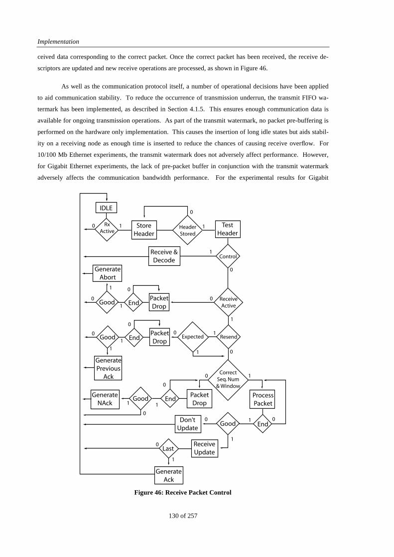
Implementation
130 of 257
ceived data corresponding to the correct packet. Once the correct packet has been received, the receive de-
scriptors are updated and new receive operations are processed, as shown in Figure 46.
As well as the communication protocol itself, a number of operational decisions have been applied
to aid communication stability. To reduce the occurrence of transmission underrun, the transmit FIFO wa-
termark has been implemented, as described in Section 4.1.5. This ensures enough communication data is
available for ongoing transmission operations. As part of the transmit watermark, no packet pre-buffering is
performed on the hardware only implementation. This causes the insertion of long idle states but aids stabil-
ity on a receiving node as enough time is inserted to reduce the chances of causing receive overflow. For
10/100 Mb Ethernet experiments, the transmit watermark does not adversely affect performance. However,
for Gigabit Ethernet experiments, the lack of pre-packet buffer in conjunction with the transmit watermark
adversely affects the communication bandwidth performance. For the experimental results for Gigabit
IDLE
RxActive
StoreHeader
ControlReceive &Decode
ResendExpected
CorrectSeq. Num& Window
PacketDrop
GenerateNAck
ProcessPacket
End
ReceiveUpdate
Last
GenerateAck
Don'tUpdate
TestHeader
HeaderStored
EndGood
GeneratePrevious
Ack
0 1 1
0
1
0
1
01
0
10
1 0
1
00
0
1 1
PacketDrop
EndGood
ReceiveActive
1
0
Good
0
0
1
1
GenerateAbort
PacketDrop
EndGood
0
0
1
1
1
0
Figure 46: Receive Packet Control
FPGA Message Passing Cluster Architectures
131 of 257
Ethernet, transmit watermark is disabled, resulting in a maximum unidirectional bandwidth of ~900 Mbps
against ~700 Mbps when it is enabled. The disabling of the transmit watermark shows the performance that
is possible. To support correct packet operations, packet pre-buffering should be enabled so that the trans-
mission watermark can be enabled while not reducing the achievable communication performance.
A total of 128 BD descriptors exist within the present implementation. These are split into two sets
of 64 descriptors for receive and transmit. The number of descriptors directly influences the message seg-
ment size that is used between nodes, with the present implementation using a message segment size of 64
packets. To increase the number of packets in a message segment, additional Block RAM memory resources
would need to be added. Apart from increasing the number of BDs that are available, a number of hardware
only updates have been added to each BD to aid the communication protocol’s operations. For transmit op-
erations, the ability to perform inline packetisation has been added. Inline packetisation is the process of
encapsulating the communication data as it moves through the network, with the update controlling the addi-
tion of the header data as the CRC value is already added to the transmit data. Performing the operations at
the network interface reduces the complexity of moving the message data from memory and adding the re-
quired message data packet header information, as described in Section 4.1.6. Inline packetisation is per-
IDLE
TxEnabled
SendPacket
NAckLatched
TimeOutLimit
End
ReceiveAck
LastWaitAck
NAckLatched
AbortError
ActivateResend
Update
AckActiveDone
AbortTimeOut
1
0 1
1
1
0
0
0 0
1
0
1
1
0
0
Figure 47: Transmit Flow Control

Implementation
132 of 257
formed on a per packet basis allowing for control over how individual packets are generated. Additional
updates have been applied to the receive BDs to perform depacketisation, the removal of the header data. As
part of the data removal, the communication protocol header data is compared with the expected values, as
detailed in Figure 46. As part of the depacketisation process, the CRC value is also removed ensuring DMA
operations write only message data to application registers. Control of the depacketisation process is sup-
ported on a per packet basis.
Communicating nodes need to know each other’s addresses so that packetisation can be performed
correctly. The message passing node identity translation gathers the network specific addresses which are
written into additional BD registers, which record the per packet MAC address that is to be used. Along
with knowing the network address and performing the encapsulation operations, an issue arises when the
communication size is smaller than a minimum sized packet i.e. message data < 43 bytes. For small packets,
decapsulation has to take into account the padded data and ensure this is not passed to the application regis-
ters. To support this, along with the MAC address being written to the BDs, the expected receive size is also
stored and used for testing incoming data. When the amount of data is less than a minimum sized packet, the
receive logic stops receiving new packet data once the expected amount of data has arrived. This ensures the
hardware application microarchitecture does not need to care about the size of the remote register transfer
operation as it will only receive the expected amount of data.
Further to data packet configuration updates, the use of control packet insertion has been investi-
gated as part of the hardware implementation. Packet insertion is the ability to insert packets as part of an
ongoing communication without corrupting any packets. This is achieved by inserting the control packet
between data packets once idle time is present on the network. The IEEE 802.3 standard requires the ability
to generate pause control packets which are inserted into the communication stream without corrupting any
transmit operations. This functionality is present in the OpenCores MAC and has been updated to generate
both message passing and communication protocol control packets. Two operations are performed with
these control packets in the hardware, the first is to accept and decode the packets independently of the re-
ceive BDs that may be configured and secondly to allow for the exchange of flow control packets regardless
of any ongoing transmit operations. The first aspect ensures control packets can be received at all times by
the node as dedicated hardware is provided to receive and decode the data. Using the dedicated control hard-
ware control packets that are received are removed from the main data stream, ensuring only message data is
moved between the network and memory. This is achieved by controlling the receive FIFO so that only mes-
sage data is loaded and processed. To operate the transmit control packet logic the destination MAC address
along with the node identity must be loaded into registers which are connected to the control transmit logic.
The control packet generation hardware uses this data to build and request insertion of the control packet for
transmission.

FPGA Message Passing Cluster Architectures
133 of 257
WISHBONE BUS
HARDWARE APPLICATION
HDL MP API
MESSAGE PASSING
STATE OPERATIONS
MESSAGE
PASSING
APPICATION
DATA
APPLICATION
MEMORY
INTERFACE
HOST
CONTROLLER
ARBITRATION
LOGIC
ETHERNET
NETWORK
CONTROLLER
MEMORY
INTERFACE
LOGIC
BLOCK
RAM
MEMORY
GMII MII
PHYSICAL LAYER
DDR MEMORY
INTERFACE
OFF CHIP MEMORY
COMMODITY
COMPONENTS
FPGA
Figure 48: Hardware System Architecture detailing how the different components are connected with
each other to provide the hardware only implementation.
4.3 Software FPGA Processor Implementation
Unlike the dedicated hardware microarchitecture, where all operations and logic have to be implemented, the
software FPGA processor implementation uses commodity components, in keeping with other software mes-
sage passing solutions that have been looked at [Fuentes '06, Schultz '06, Pedraza '08]. For the FPGA proc-
essor solution, only a soft processor is investigated as this approach allows for more scalability in the FPGAs
that can be used. The Xilinx MicroBlaze processor [Xilinx '08b] is used in the implementation, as it is used
by other similar projects. The MicroBlaze system comes with a wide range of development tools – the
Embedded Development Kit (EDK) – and its implementation is tailored to the FPGA logic.
This section details how the MicroBlaze processor and additional ancillary logic has been used to
implement the point-to-point remote register transfer operations in software. The software implementation is
developed to interface with and accept the HDL MP API communication operations which need to be con-
verted into software structures which the processor can access. This operation is performed as the HDL MP
API has been developed to perform remote register transfer operations between distributed hardware mi-
croarchitectures, independently of the physical mechanism that performs the data exchange. The interfacing
of the processor with hardware applications in this manner is different to the other software message passing
approaches which only look at exchanging data between software running on the processor, not at accessing
and exchanging data between hardware application microarchitectures.

Implementation
134 of 257
4.3.1 Hardware Architecture
An FPGA processor node consists of a MicroBlaze Processor, a HDL MP API enabled application, the Net-
work controller, Network Packet Buffer memory and ancillary logic which allows each unit to interact in a
controlled manner. This is similar to the architecture presented by Fallside and Smith [Fallside '00] for a
network connected FPGA. This section details the architecture that allows these units to function correctly
to perform a requested message passing remote register transfer operation. Only communication from appli-
cation buffers is supported as the implementation environment and required operational overheads of the
processor remove the ability to support network zero-copy DMA operations with external memory.
MicroBlaze Processor
The MicroBlaze processor, v7.10.d [Xilinx '08b], used for the FPGA processor implementation is a soft-
processor that is implemented using reconfigurable logic. This allows the processor to be implemented on a
wide range of FPGAs once enough logic exists. The MicroBlaze processor is a 32-bit RISC processor, im-
plemented using the Harvard architecture. The use of the Harvard architecture improves processing perform-
ance as both instruction and data can be read into the processor concurrently. The instructions and data are
compiled from the implemented control software and are loaded into dedicated memory accessible only by
the processor across a dedicated burst bus, the Local Memory Bus (LMB). For the implementation, Block
RAMs are used to store the processor control program data, with the size of this memory kept as small as
possible to reduce resource usage. As the attached memory is only accessed by a single processor in this
project, the same dual port Block RAM memory is used for both the application and data values, with data
accessed through one port and instructions through the other.
The implemented processor uses a 5 stage instruction pipeline, with 16 KB of memory attached to
the processor, using a total of 8 Block RAMs. The processor is connected to all system elements by the
PLBv46 bus [Xilinx '09a]. This bus is designed to be more efficient than the more common OPB bus how-
ever, the MicroBlaze processor as implemented is not able to perform burst operations across the PLB bus.
HDL MP API Processor Bridge
The communication interface of the HDL MP API has to be connected with structures that the processor is
able to read and access. The communication interface consists of approximately 110 signals for both send
and receive while the processor is only able to access 32-bits of data at a time. Two architectures were inves-
tigated for translating the signals – one using FSL links and the other using memory mapped registers that the
processor reads and tests. Issues with using FSL links, coupled with additional processor logic overheads to
use FSL links results in the memory mapped registers approach being implemented to interface the FPGA
processor with the HDL MP API. The memory mapped registers have been implemented as a single Block
RAM which the processor connects with using PLB compliant Block RAM connection elements.
FPGA Message Passing Cluster Architectures
135 of 257
The development of the interface logic sees the use of both ports of the Block RAM. One port is
connected to the processor where data is accessed, the other is accessed by the HDL MP API translation
logic. Based on the data that is present in the Block RAM, the FPGA processor software has been developed
to perform the directed remote register transfer operations. This logic interfaces three operational units with
the single port, send and receive command operations and the reading back of any information the processor
has written into the Block RAM – node identity, node count, communication status, etc. The logic operations
at the HDL MP API interface must ensure fair access for the three interface units. This is performed using a
round robin arbitration which gives each unit access to the Block RAM interface to update and test the data.
The operations of the HDL MP API translation logic are transparent to the application as these operations
occur between the interface and the processor.
For send and receive operations, the control data must be written into the Block RAM before writing
the communication request information to avoid race conditions where the communication is active before
the control data is present. A total of four memory address data lines are used for both send and receive. The
interface Block RAM has been partitioned to reduce implementation complexity with the send, receive and
processor data all residing in predefined memory locations. Associated with the send and receive interface
logic, are dedicated translation state machines which are responsible for serialising the HDL MP API com-
munication signals into the structures loaded into the Block RAM. The collective communications that an
application may need are implemented on top of these translation state machines ensuring the necessary con-
trol structures will be generated if a collective communication is requested.
Processor Network Bridge
The processor is interfaced with the network control logic in two ways. The first sees the FPGA processor
interface with the Wishbone Bus slave interface across a PLB to OPB bridge. The second interface sees the
FPGA processor and Wishbone Bus Master interface exchange data through a network packet buffer. This is
required as the Wishbone Bus and the PLB Bus are not compatible while the use of the same network con-
troller between the hardware and FPGA processor solution ensures only a single network controller is im-
plemented. The Wishbone-OPB bridging is possible without much modification however the performance of
the OPB is limited. As the slave interface does not require a high performance interface, the PLB-OPB-
Wishbone bridging approach was taken. The Master interface, however, is more performance intensive as it
is required to move data from network buffers to system memory. Operating at gigabit rates, the OPB bus
does not have enough bandwidth to support the correct movement of data. This requires the use of the PLB
bus but the Wishbone and PLB busses are incompatible, while the need to store network data is still required.
The network buffer supports Wishbone signalling on one interface and PLB memory access on the other.
This allows the Ethernet controller and FPGA processor to exchange network data. The software running on
the FPGA processor needs to read all data that moves between the network and the application microarchitec-
ture so the use of the buffer between the network and the processor does not directly add overheads.
Implementation
136 of 257
The Ethernet controller uses interrupts to signal events that occur on the network. Using these inter-
rupts with the MicroBlaze processor resulted in an unspecified freezing of the processor while not advantag-
ing the software implementation operations. Hence, the use of polling operations to read the Ethernet inter-
rupt registers was used to know when a network related event has occurred. As the processor is only respon-
sible for interfacing with the network and will not be required to support other operations this will not impact
the overall performance of the application, rather polling operations should advantage the processor response
time, as polling operations are quicker than interrupt operations [Mogul '97].
Network Packet Buffer
While developing the software solution, it became apparent that complete DMA operations were not possible
between the network and the application memory. This arises as data copying is required as part of the soft-
ware packetisation operations. As data must be buffered between the application registers and the network
MAC, a network packet buffer was implemented. This buffer is configured to store a total of eight packets
which are configured as four maximum receive packets, two maximum transmit packets and two minimum
sized transmit packets. The difference in packet configuration breakdown reflects the operations that occur
across the network. Receive operations can occur at any time and the size of the data being received is not
always known in advance. As the amount of resources that should be assigned to the network buffer should
be kept to a minimum, the use of partitioned memory as opposed to an elastic configuration, was appropriate.
Using partitioned memory reduces the software complexity as each successive receive is configured to use a
pre-defined memory address.
The partitioned space is configured for four receive buffers, with an array set to store the addresses
that are to be used. The two maximum transmit buffers are located in the next free memory above the re-
ceive partition. Finally, as control packets are used and necessary, dedicated transmit buffer memory is set
aside for these packets again with a preset memory for where they should be stored.
4.3.2 Software Functionality
The communication operations running on the processor have been implemented using C. The software is
responsible for testing the HDL MP API interface logic and generating the remote register transfer operations
which support the distributed application hardware operations. It is also responsible for configuring and test-
ing the network system so that communications behave correctly. Software code development has resulted in
generating code with a memory requirement of approximately 13 KB when compiled with the highest opti-
misation levels and without debug information.

FPGA Message Passing Cluster Architectures
137 of 257
BRAM
NETWORK
PACKET
BUFFER
LMB
PLB
HDL MP API
BRIDGE
HARDWARE APPLICATION
HDL MP API
MESSAGE
PASSING
APPICATION
DATA
GMII MII
PHYSICAL LAYER
COMMODITY
COMPONENTS
FPGA
MICROBLAZE
PROCESSOR
SOFTWARE
BRAM
MEMORY
BRAM
ARBITRATION
LOGIC
ETHERNET
NETWORK
CONTROLLER
S M
PLB-OPB
BRIDGE
PLB
OPB
BRAM
WB
Figure 49: Software FPGA Processor Architecture highlighting how the different components are
interconnected as well as the SoC protocols that are used. BRAM signals are generated by PLB –
BRAM conversion logic which are not shown to reduce diagram complexity
Communication Operations
The principle functionality of the software solution is to perform and configure point-to-point remote register
transfer operations that the hardware application microarchitecture will request through the HDL MP API.
As detailed in the hardware architecture (Section 4.3.1), the software accesses the communication buffers
that are used to translate the message passing HDL MP API interface signals into processor readable values.
Based on the values that are read, the point-to-point communication request is processed and the resulting
packets generated and communicated. The software communication operations follow the message passing
state machines that have been described (Section 3.1.1), but unlike the hardware configuration, all operations
are performed in software, requiring the storage of state information between loop iterations. This is
efficiently achieved by storing the message passing state information in the interface Block RAMs as this is
memory that is free to be used while for correct operations this memory is continuously read and processed.
The processor is configured to continuously loop and test the interface values to see if further operations need
to be performed. As part of the testing operations, the network interrupt register is polled to reflect any
changes that have occurred on the network. The network state information is used by the processor to know
if the present communication state is accurate and if new operations are required e.g. the synchronisation is
now complete, proceed with the data communication.
Implementation
138 of 257
Once the processor identifies that a remote register transfer operation is to be performed, it is re-
sponsible for performing all network packetisation operations for the exchange of data between nodes. On
the transmitting node, the processor is responsible for reading data in from application memory and encapsu-
lating the data with packet header data so that the communication can occur. On the receiving node, the
processor is responsible for decapsulating the packet and moving the data into the application buffers. For
the data copy operations, to try to minimise their overheads, a memory aligned copy operation is used with
application data copied in 32-bit blocks to the network buffers. To achieve this, the packet header informa-
tion is realigned i.e. packet starts at hex 0003 but data starts at hex 0014. Using this alignment for data copy-
ing reduces the number of operations that have to be performed as packet header information can easily be
byte aligned given the structure of that data, while application data copying, constituting most of the packet
operations, are more efficiently performed word aligned. As data copy operations place a high burden on the
communications, packet pre-buffering is used with a new packet created while the preceding packet is being
communicated. This allows packetisation operations to overlap with communication operations.
As well as performing packetisation operations, the software must also test all packets that it re-
ceives to identify control packets and data packets. All packets that are received are stored in known ad-
dresses within the network packet buffer, allowing the software to read the packet type information from a
known buffer address. If a control packet is recorded in the network buffer, the necessary information is read
out and stored. Both flow control and message passing synchronisation packets are possible and along with
identifying the type of the packet, the control field data is tested to see what the packet data is meant to be
interpreted as. In the software solution, packet testing and checking is only performed after the network has
generated the receive interrupt, telling the processor a packet is present in the network buffer. As the inter-
rupt is generated after the packet has been received correctly and passed the Ethernet CRC test, the software
solution does not gain anything from using an internal control packet CRC and as such, does not generate nor
test for one. This means, in the present setup, that the hardware and FPGA processor solutions cannot be
used in a single environment but reduces the overheads of the FPGA processor implementation. As well as
testing the packets within the software and updating software state information, the processor must also write
control information into the HDL MP API interface logic so that the hardware application knows when a
remote register transfer operation is complete. To ensure the correct operations are acknowledged by the
hardware application, distinct values are written by the software into the interface buffers. The values written
in are picked up by the hardware and HDL MP API interface signals generated to inform the hardware appli-
cation microarchitecture that the remote register transfer operation is complete.
All software functionality details presented above relate to how the processor performs message
passing interface operations and does not detail how it controls the network hardware and configuration reg-
isters. To support the operations of the network hardware, methods have been developed which configure the
network registers correctly to setup the communications. The use of these methods allows the software sys-
tem a degree of flexibility for the network controller that is used as it becomes trivial to update register map-
pings while not requiring a change to higher level operations.

FPGA Message Passing Cluster Architectures
139 of 257
Network Control Hardware Operations
To perform a communication operation, the transmit and receive control registers and BDs of the network
must be configured. As this operation is common regardless of whether a data packet or control packet is
being exchanged, dedicated methods have been implemented which configure the registers as directed by the
method parameters. Both a send and receive method have been implemented as slight configuration differ-
ences exist between each communication style.
As part of the development of the control hardware methods, an issue was noticed during large mes-
sage communications when the system would stop working. Investigations showed an issue with the inter-
rupt / acknowledgement logic of the send method where it was unable to find the end of a communication
correctly. The issue was caused by how control packet transmissions were tested for and removed from the
BD stream of packets. To resolve the problem, a free BD bit was updated to record if a transmission was a
control packet or a data packet. This update does not affect the hardware solution as the bit location was a
reserved location not used by the controller previously.
Initialisation Operation
The initialisation routines of the FPGA cluster are performed in software, with the address list stored in a
data array. This allows data to be stored and read back efficiently from LMB memory during packetisation
operations. The use of Block RAMs similar to the hardware solution was examined however, the use of ex-
ternal memory increased the amount of operations on the PLB without any directly discernable advantages as
the LMB Block RAMs are already implemented and provide a more efficient interface than the PLB Block
RAM interface.
Software Limitations
The software as implemented is able to generate data which is usable as part of the evaluation requirements.
However, a number of limitations are present in the implementation which reduce the stability of the soft-
ware solution against the hardware solution. The first major limitation is the limited flow control operations
that are implemented. Synchronisation and flow control acknowledgement data is generated as per the com-
munication protocol requirements. However, the identification of dropped packets is not implemented. The
required timer logic is not present as part of the software solution. The second limitation is the requirement
of the software to copy data from the application buffers through to the network packet buffers. Although the
cost of performing this has been limited by the use of word aligned copies and pre-packet buffering, the
overheads of performing this operation still reduce the maximum achievable communication bandwidths.

Implementation
140 of 257
HardwareApplication
MessagePassing
HardwareSoftware
Processor
MessagePassing /
CommunicationSoftwareInterconnect
ControlHardware
InterfaceLogic
NetworkPacket Buffer
HardwareFlow Control
Interconnect
Message
Passing
Layer
Interconnect
Protocol
Layer
Media AccessController
Application Logic
and Message
Passing Interface HDL MP API
HardwareImplementation
SoftwareImplementation
Figure 50: Message Passing Implementation Architectures showing the flow of information through
each architecture and how they compare with each other. This is presented at a high level to show how
the two architectures compare side by side.
4.4 Management Node
The management node is used to provide user interface operations for configuring and accessing the distrib-
uted hardware application microarchitectures as part of the sequential operations of a fork-join parallel algo-
rithm. The management node supports the exchange of data between the user and computation logic, the
initialisation operations that facilitate remote register transfer operations between the hardware application
microarchitectures and parameter operations to direct the computations a hardware application microarchitec-
ture should perform. The management node provides software methods which are able to communicate and
exchange data with the hardware application microarchitectures in a controlled manner using the message
passing and communication protocols. The management node is implemented on a commodity microproces-
sor, running Linux, and using standard network libraries and methods – sendto, recvfrom – to perform the
communication operations. In addition to providing an ability to interact with and initialise data across the
distributed hardware application microarchitectures, the management node is also used during system initiali-
sation to perform the sorting and organising operations needed to collate the MAC addresses for node iden-
tity generation.

FPGA Message Passing Cluster Architectures
141 of 257
4.4.1 Point-to-Point Remote Register Transfer Operations
The point-to-point communication operations are the most important message passing code that needs to be
implemented by the management node. The point-to-point communications facilitate the transfer of data to
the hardware application microarchitectures, and the microprocessor software implementation must be able
to exchange data correctly with them. Like the HDL MP API before it, the operations of the management
node are abstract from the physical interconnect that is used. This is achieved through the use of network
libraries and has been tested through the range of Operating Systems the microprocessor software has been
run on, Ubuntu 6.06 – Ubuntu 8.10. A custom implementation of the software has been undertaken to ensure
the management node is able to exchange data with the FPGA compute units using the custom communica-
tion protocol that is used. Message data communications are performed using standard SendTo and
RecvFrom software primitives. The message passing software is implemented around these operations, sup-
porting correct data communication and exchange operations. As part of these operations, fragmentation as
previously present is also supported as is the message segmentation operations that are required to support
communications between all connected compute units.
As the objective of the management node is to support sequential operations of fork-join parallelisa-
tion, a means to interface with the computation logic provided by interconnected FPGAs, certain limitations
exist in the microprocessor software. The first of these is the limited support for communication flow control
operations. While communications between the management node and the FPGA computation logic use the
message passing and communication protocol information, no support for flow control is present. This does
not limit the amount of operations that can be undertaken between the management node and the FPGA
nodes as Ethernet’s communication stability is high enough for most communication operations that will
occur between the management node and the FPGA nodes. As the management node is not used in ongoing
communication operations, the complete implementation of the flow control operations was seen as beyond
the scope of the project and has not been implemented.
4.4.2 Initialisation Role
As well as providing an easy to use software interface between the user and the distributed hardware applica-
tion microarchitectures, the management node plays a role in the initialisation and data distribution opera-
tions. Data distribution operations are covered as part of the point-to-point operations above, while the role
of the management node in the initialisation are described here.
The initialisation operation across the FPGA compute units commences once the FPGAs have been
programmed and the microprocessor software interface application is started. One of the first operations that
the microprocessor software must perform is the initialisation of the communication interface of the HDL
MP API of the FPGA nodes. At the start of the FPGA initialisation operation, the management node is un-
aware of the MAC address of any nodes connected to the switched network. This requires the management
node to generate a broadcast packet which all connected compute units listen for and respond to, similar to
Implementation
142 of 257
operations of Address Resolution Protocol (ARP). In response to this broadcast packet, the FPGAs reply
with their network specific address which the management node stores in a MAC address list which will be
distributed back to the FPGAs. As part of this operation the network specific addresses are sorted based on
the order packets are received at the management node. This reduces the sorting operation complexity as the
switched network serialises the data and forces an order on the data that is received. Once the expected num-
ber of nodes have responded to the initialisation request, and with the MAC address list built, the manage-
ment node distributes the MAC address list to all connected FPGAs again using a broadcast packet. As de-
tailed previously, the receiving nodes decode this packet and generate the network address to node identity
translation that is needed to provide an abstract message passing node identity as part of the HDL MP API.
4.5 Matrix Multiplication Architecture
Parallel matrix multiplication is being used to test the functionality of the HDL MP API in performing re-
mote register transfers between distributed hardware application microarchitectures. Design details that can
be used to perform this have been presented in Section 3.5.1. The implementation of the microarchitecture is
detailed here. FPGA matrix multiplication is concerned with taking the parallel matrix multiplication algo-
rithms and applying it to individual and multiple FPGAs. To perform this efficiently, FPGA matrix multipli-
cation uses multiple processing elements that are interconnected to perform the computations. A practical
configuration for this is to interconnect each processing element as a single linear array [Kumar '91, Zhuo
'04], where it is possible to add or remove processing elements with minimal design reworking.
The basic element for FPGA linear array matrix multiplication is the processing element. The proc-
essing element performs the multiplications and additions, while also providing temporary memory storage
for both computation and result data. A processing element consists of the following basic logic units, the
multiplier, the adder, storage, and the necessary control logic to operate these units correctly. The processing
element also requires interface signalling that will allow it to operate as part of the linear array. The neces-
sary interface signalling must cater for and allow additional units to be added or removed with ease. Fused
multiply-accumulate floating point units have been shown to reduce the FPGA logic footprint [Dou '05].
Fused multiply-accumulate units can also reduce the computation latency as there is no need to perform nor-
malisation on the floating point number between the multiplier and the adder. Furthermore, floating point
data processing of the addition number can start before the multiplication is completed. This reduces the
overall computational latency while also improving the computation times.
4.5.1 Linear Array Matrix Multiplication Architecture
Linear array matrix multiplication, based on that presented in [Zhuo '04], has been implemented to perform a
system verification when a distributed hardware application is run across the FPGA cluster using the HDL
MP API to support remote register transfer operations. The implemented linear array is parameterised both
at synthesis time, controlling the number of processing elements in the linear array, and during computations.

FPGA Message Passing Cluster Architectures
143 of 257
The A and B matrix storage sizes are controlled by run time parameters, uploaded by the management node
during computation initialisation. Controlling the number of linear array units with synthesis constraints aids
verification simulation tests by allowing the easy targeting of smaller linear array sizes.
Processing Element
The processing element logic has been implemented as shown in Figure 51. All storage units in a single lin-
ear array use Block RAM structures. B matrix data is prefetched when possible, improving the computation
C Addr InC Addr Out
BRAM Interface
FIFO ControlSignals
FIFO
BRAM Interface
BRAM Interface
Floating PointMultiply Accumulate
Processing Unit
A Shift In
A_in Data
B Shift In
B_in Data
BRAM
CounterEN
Write
CounterEN
Write
FIFO CtrlSignals
CounterEN
Write
CounterEN
Write
0
C Result Out
A Shift Out
A_out Data
B Shift Out
B_out Data
C Result In
BRAM Interface
BRAM
Shift ControlUnit
Figure 51: Base Processing Element Structure

Implementation
144 of 257
efficiency of the linear array. The B matrix Block RAM is partitioned into two segments, each to a maxi-
mum size of 256 floating point numbers. The partitioning, in connection with the dual port Block RAM, al-
lows one port to be used for the present computations while the other port is used to store the next iteration’s
prefetched data. The algorithm that is used for the linear array reuses the B matrix data as efficiently as pos-
sible while A matrix data is used only once and re-read from memory if required. To efficiently reuse the B
matrix data the Block RAM address structure is directly accessed while the single use of the A matrix data
allows for the use of a FIFO as an efficient data storage structure. Processing element control logic ensures
correct operation of the necessary address pointers and FIFO control signals.
Computations are performed when appropriate data is present in both the A FIFO and the B memory
structures. The computations occur concurrently to the continued loading of additional A matrix data. B
matrix pre-fetching is performed once all necessary A matrix data has been read in and stored in the FIFO.
The computation performance improvement that is possible depends on the amount of B matrix pre-fetching
overlap that can be performed during the present iteration’s computations. Ideally, all data for the next itera-
tion of the B matrix should be stored for the most efficient computation operations. All A matrix data is read
in before B matrix data pre-fetching is performed to ensure overall operations behave as required throughout
the computational phase. For the linear array that is implemented, the compute units read in data every clock
cycle while main memory reading latency can be up to 50 clock cycles.
The compute units of the processing element are single precision floating point Xilinx Coregen
[Xilinx '09b] multiply and addition units . The multiplication unit has a depth of 5 and the addition unit has a
depth of 6. The multiplier and adder are directly connected with each other forming a single multiply-
accumulate unit with three inputs, multiplicands A, B and accumulated C matrix value. For efficiency, the C
matrix data is only read in when it is needed by the adder. This removes temporary pipeline storage that
would be needed if the adder data were read in concurrently with the A and B data. This also uses the C ma-
trix storage elements efficiently. To allow for the efficient use of the C matrix storage, both ports of the
Block RAM are again used, with new result data written into one port, and the necessary accumulated data
read from the other. The horizontal data decomposition allows a processing element to perform all computa-
tions on a row, column of the respective matrices without requiring the temporary unloading and reloading of
the C matrix data with main memory. Operating in this manner reduces the main memory bandwidth that is
needed per processing element.
Linear Array Architecture
Each processing element contains interface logic which allows for the interfacing of multiple processing ele-
ments to create the computation linear array. Data buffering is used by each processing element in the linear
array to ensure a higher application timing closure is achieved. Data buffering increases the latency for data
movement through the linear array however, a higher timing closure allows for more data computations
across the entire linear array. The presently active processing element signals subsequent processing ele-
ments once it has performed all necessary data loading. Control of how much data is processed by each unit
is controlled by the parameters that are uploaded as part of the overall linear array system operations. An

FPGA Message Passing Cluster Architectures
145 of 257
overview of the linear array configuration is shown in Figure 52. Data is shifted in from the first processing
element to the last element with each successive unit enabled once the preceding unit has received all its data.
The first processing element is that unit which connects to the system memory, here external memory,
through the HDL MP API.
Computation results are shifted back through the linear array such that the result data in the first
processing element is written into memory first. Unlike the reading in of the data, the result writeback in-
volves all units concurrently shifting data from the last element to the first element and finally out to the cor-
rect memory location where it is to be stored. The fact that all units shift result data concurrently, requires
the use of both ports of the temporary storage Block RAMs to efficiently move data through the linear array.
This configuration removes the ability to perform concurrent computations and data result writeback. This
deficiency can be removed if the temporary storage is split into two equal sized memory units, one used dur-
ing the result writeback while the secondary unit stores new computation data. For correct operation of this
though, less temporary result storage will be available, reducing the amount of computations that can be per-
formed by a given processing element. The impact of using a single storage unit versus two storage units
could be investigated further but for the purpose of system verification, the use of a single storage element for
the result matrix is acceptable.
Further to the individual control units present in each processing element, a linear array control unit
is present which maintains state across the linear array and ensures the correct operations are performed.
Development of the control logic does not assume any particular number of processing elements will be pre-
sent in the linear array. Necessary synthesis parameters are used in connection with the uploaded computa-
tion parameters to ensure correct operation across the linear array. The control logic is responsible for cor-
rectly signalling the interface ports of the first linear array element and controls the matrix data address
pointers to ensure the correct computations are performed on the correct data. The algorithm for the control
unit is presented in Table 5, Section 3.5.1. Limited storage is available across the linear array, so to ensure
large matrix sizes can be computed on a single node, a further control unit is present which updates and gen-
erates the appropriate base address pointers for each iteration across the linear array. This control unit per-
forms the appropriate linear array data decomposition that is used for the computations. The communication
data decomposition is based on horizontal data decomposition while, to remove the data dependencies of the
floating point units, vertical data decomposition is used across the linear array. To ensure correct operation
of this data decomposition the outermost control unit decomposes the memory system into appropriate seg-
ments which the linear array then performs computations on.
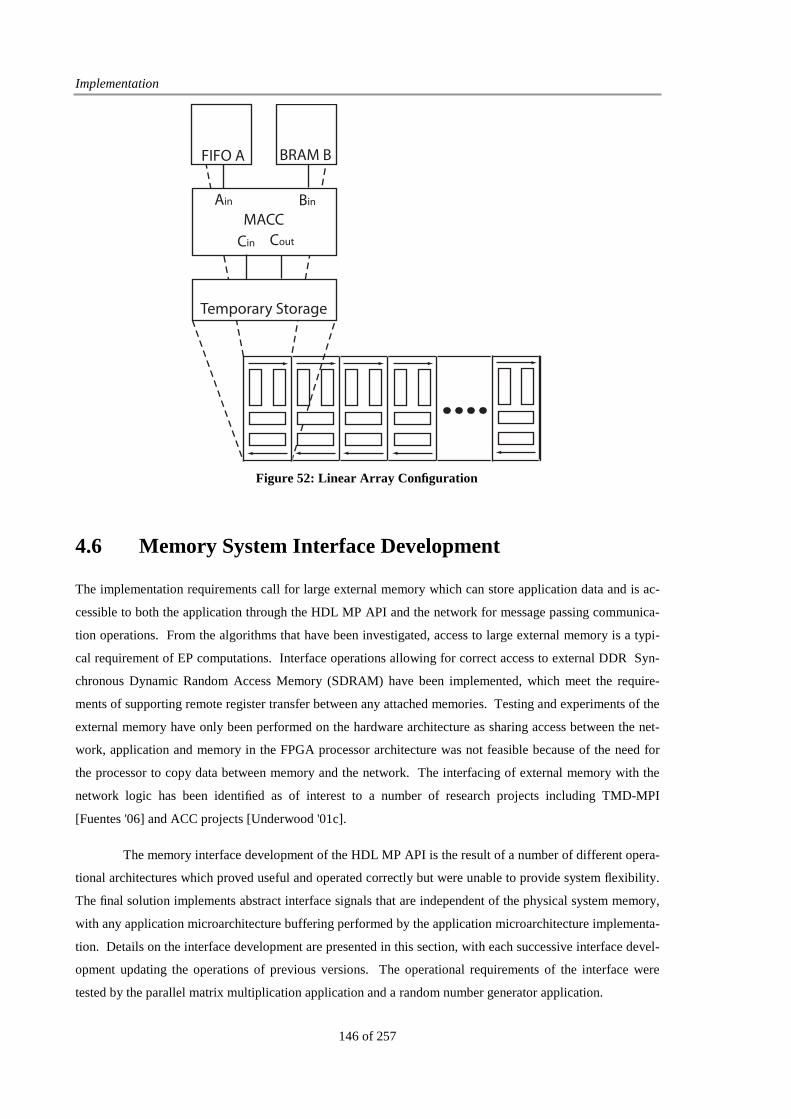
Implementation
146 of 257
4.6 Memory System Interface Development
The implementation requirements call for large external memory which can store application data and is ac-
cessible to both the application through the HDL MP API and the network for message passing communica-
tion operations. From the algorithms that have been investigated, access to large external memory is a typi-
cal requirement of EP computations. Interface operations allowing for correct access to external DDR Syn-
chronous Dynamic Random Access Memory (SDRAM) have been implemented, which meet the require-
ments of supporting remote register transfer between any attached memories. Testing and experiments of the
external memory have only been performed on the hardware architecture as sharing access between the net-
work, application and memory in the FPGA processor architecture was not feasible because of the need for
the processor to copy data between memory and the network. The interfacing of external memory with the
network logic has been identified as of interest to a number of research projects including TMD-MPI
[Fuentes '06] and ACC projects [Underwood '01c].
The memory interface development of the HDL MP API is the result of a number of different opera-
tional architectures which proved useful and operated correctly but were unable to provide system flexibility.
The final solution implements abstract interface signals that are independent of the physical system memory,
with any application microarchitecture buffering performed by the application microarchitecture implementa-
tion. Details on the interface development are presented in this section, with each successive interface devel-
opment updating the operations of previous versions. The operational requirements of the interface were
tested by the parallel matrix multiplication application and a random number generator application.
FIFO A BRAM B
MACC
Cin Cout
Ain Bin
Temporary Storage
Figure 52: Linear Array Configuration

FPGA Message Passing Cluster Architectures
147 of 257
A number of solutions for memory interface development have been explored from a single applica-
tion interface for all memory accesses to multiple parallel accesses through the provision of dedicated appli-
cation memory interface blocks. The single application interface is used as the preferred interface since op-
erational difficulties with the other implementations made these interfaces impractical. The operational re-
quirements of the single memory interface were developed from refinements of each successive implementa-
tion approach that was explored, with the progression shown in Figure 53. The various memory interface
developments are connected with the development boards that are used by the project, with the memory in-
terface developed primarily for correct operation with the single channel DDR SDRAM DIMM of the XUP-
V2P [Xilinx '05] FPGA development board.
DDR SDRAM memory requires specific functionality to operate correctly with operations provided
by a dedicated DDR memory controller. Two controllers have been used in this work, the OpenCores DDR
memory controller [Winkler '09] and the Gaisler AMBA DDR Controller [Gaisler '07a]. The OpenCores
controller required the implementation of SoC bus interface logic for correct operation, while the Gaisler
controller uses the AMBA Bus. DDR memory clock restrictions require the use of a dedicated clock for the
memory path while the application space may use a different user clock. For the OpenCores controller, the
cross clock domain operations had to be implemented while the AMBA controller performs all cross clock
domain operations internally, with the AMBA bus interface operating off the user clock. The application
interface development was based on using the OpenCores controller while either controller can be used in the
final configuration.
HDL MP APIApplication
FIFO
Memory
HDL MP APIApplication
FIFO
Memory
Heap
HDL MP APIApplication
Memory
Interface Refinement Progression
Cache Buffer
ApplicationImplementation
Space
Figure 53: Memory Interface Developmental Configurations showing the interface refinements that
have been performed to arrive at the final configuration.
4.6.1 FIFO Interface development
The use of FIFO buffers to exchange data between devices influenced the first development iteration. To use
this configuration the application instantiated the FIFO logic, with the application interfacing to Wishbone

Implementation
148 of 257
signals on one side and DDR memory signals on the other which connected to on-FPGA routing logic before
interfacing with external memory. The routing logic development allowed multiple such units connect to a
single memory and ensured they shared memory access correctly. The FIFO within the application space
allowed for temporary storage as it was implemented to perform one complete access of external memory i.e.
one access could result in a single transfer up to a burst length of 8 which with a 32-bit data path results in a
transfer of 256-bits on a single access. Testing on the use of the FIFO showed that it operated correctly in
relation to accessing memory. However, the limited application interface operations meant an application
was unable to arbitrarily access memory stored in the FIFO. This limited the usability of the FIFO buffer and
lead to a new iteration on this interface, a Heap/FIFO configuration.
4.6.2 Heap/FIFO Interface Development
A heap/FIFO architecture was developed as a refinement of the FIFO only memory interface logic. The
heap/FIFO structure overcomes the limitation of arbitrary buffer address access, by allowing the application
control the order of data access, unlike the FIFO only approach which can only process data in a linear order.
The FIFO interface to memory was maintained as external memory accesses occur sequentially. Using the
heap/FIFO architecture and classical matrix multiplication, application testing was performed. Testing of the
heap/FIFO architecture under application requirements revealed a number of deficiencies for using multiple
heap/FIFO interfaces. These deficiencies included coherency between multiple buffers, network communica-
tion access to the buffers and synthesis routing difficulties caused by the DDR routing logic.
Coherency between buffers requires the application programmer to know what data is in which
buffer at all times in the computations. The development of the routing logic between the buffers and mem-
ory did not support any coherency protocols as these are beyond the scope of the research and other deficien-
cies of the instantiated buffer configuration meant no further developments were undertaken to address or
resolve the coherency concern. As well as the coherency concern, the size of the interface buffer meant it
could not hold a complete network packet. This would result in packet data being split across both external
memory and application buffers. For a correct communication to occur, the network controller would need to
perform a DMA scatter/gather to merge all the data together correctly, or force the application microarchitec-
ture to create all register transfers in application specific buffers. Again, this was viewed to be beyond the
scope of the research question and was not undertaken. As the scale of the work involved in correctly con-
figuring access for multiple interfaced buffers was becoming very complex with no discernable advantage for
supporting remote register transfer from either the programmer’s or system operation’s perspective, the use
of instantiated buffers was stopped. Knowledge from these two architectures was brought into the next de-
velopment iteration which implemented a single memory interface which could be accessed by both the net-
work and the application while providing coherency of access for both.
FPGA Message Passing Cluster Architectures
149 of 257
4.6.3 Coherent Interface Development
Flaws in the initial memory interface approach resulted in a rethink of the physical layout and access pattern
for both the application and the network. Previous approaches looked to provide explicit memory interface
buffers as part of the application space with the programmer performing explicit buffer operations to ensure
correct memory coherency was maintained. From application experiments, the explicit memory operations
added to the complexity of implementing the hardware application microarchitectures on each compute unit.
These operations were further compounded by the remote register transfer access operations which may or
may not require the application buffers be flushed to ensure correct data is exchanged between nodes.
To support external memory, a new approach was taken which sees a single memory interface con-
troller implemented which, through the use of cache protocols, performs the translation between the on-
FPGA Wishbone Bus and DDR memory interface signals [Hennessy '03]. Cache protocols ensure efficient
translation between the external memory and the internal bus structures while providing a coherent buffer
which can be shared between the network and the memory interface of the HDL MP API. To operate cor-
rectly, the HDL MP API memory interface implementation takes its signals and converts them combinatori-
ally into the Wishbone bus signals used for on-FPGA operations. Two implementation approaches for the
memory interface controller have been tested. The first looks at a high performance interface, based on clock
speed and memory burst operations, while the second is based on the AMBA DDR controller and the neces-
sary interface logic to make the memory interface coherent for both network and application accesses. Op-
erational ideas between the controllers are similar in that they are based on using cache principles for manag-
ing and buffering data between the on-FPGA interconnect and the external DDR memory.
High Performance Interface
The high performance memory interface controller looks to operate at 133 MHz with a burst length of 8. A
single access results in a transfer of 512-bits from a 64-bit DDR DIMM module. Development and imple-
mentation of the high performance controller is based on reducing the cost of a memory access while provid-
ing the Wishbone Bus protocol interface. Using the OpenCores DDR memory controller, a cache based
Wishbone Bus slave interface was implemented which allows the controller function correctly as part of the
SoC. The interface logic implementation allows for the user clock domain of the Wishbone interface and a
memory clock domain, running at 133 MHz. All operations for cross clock domain logic are performed
within the controller, while as with the network FIFO buffers, dual port Block RAMs provide the datapath
cross clock domain operations. To ensure enough data can be concurrently accessed for a single memory
access, 4 Block RAMs have been connected in parallel giving a memory datapath of 128-bits, while a 32-bit
datapath is used for the Wishbone Bus. For the high performance controller, the Block RAM approach gives
128 unique cache buffer lines. All control and cache operations transit between the clock domains using
standard cross clock domain operations. The memory interface controller operates a cache writeback policy
when an address miss occurs. This policy requires a write followed by a read once an address miss is identi-
fied. Address misses are generated based on comparisons with stored address tags and address line informa-
Implementation
150 of 257
tion. This data is stored in the Wishbone clock domain to make comparison operations easier. Once a miss
has been identified – compulsory, conflict or capacity – the writeback operations are performed.
Simulations showed the developed controller to function correctly. However, cross clock domain
issues and clock selection operations that are performed by the high performance interface did not function
properly when running on the hardware. Different approaches to resolve these issues were taken, including
mapping the controller operations to a set area of the FPGA and locking the different clock buffers to specific
locations on the FPGA. As the operations of this controller were unstable, it could not be used reliably.
However, application computation simulations showed that this approach met the requirements to interface
both the network and the application with the memory units for correct operation.
AMBA Standard Interface
Synthesis and timing issues with the high performance interface necessitated the use of a more stable and
operational controller. The Gaisler AMBA DDR memory controller [Gaisler '07a], operating at 100 MHz
with a burst length 4, is used to provide stable access to external memory. Translation logic is required be-
tween the AMBA Bus and the Wishbone Bus with the cache buffer approach used to perform this. The cache
buffer used with the AMBA architecture is a 2-way set associative cache, with a Least Recently Used (LRU)
policy deciding which data to flush when a miss occurs. A dual port Block RAM is used per set associativ-
ity. The internal operations of the AMBA controller perform all cross clock domain operations by using two
FIFOs, each consisting of 4 dual port Block RAMs.
Coherent Interface Refinements
Testing of the operations of the AMBA memory interface controller, and by extension the high performance
controller, showed a lower than expected performance. To address the performance concern, two refine-
ments to the operations of the controller were undertaken. The first of these involves tagging data within the
cache based on whether the memory data will be modified and the second is based on using memory aligned
burst operations for data movement across the Wishbone Bus structures.
Data tagging is used to mark data that is modified against data that is not. If a cache line miss oc-
curs but the data in that line is the same as in external memory, there is no requirement to flush the data back
as it is not any different. This arises if data is only read and used in computations, but is not updated with a
new result e.g. network transmit data, matrix A or B in matrix multiplication. Rather, the new data that is
requested can be read in immediately. This reduces the cache access overheads that are performed on an
address miss. Testing of data tagging revealed a corner case when only part of the data in a given cache line
was modified. When this happens, the entire line is tagged as modified and on a miss the entire line flushed
back even though only part of the data has been modified. The entire line is flushed back to reduce the im-
plementation complexity of selecting which data to writeback and which data not to writeback.

FPGA Message Passing Cluster Architectures
151 of 257
Burst operations provide the most efficient use of the on-FPGA SoC, with the Gaisler memory con-
troller supporting burst operations natively. All Wishbone Bus interconnect structures have been updated to
provide burst operations, with the memory aligned network accesses ensuring an efficient use of the inter-
connect for both the application and the network. The use of memory aligned accesses improves the per-
formance of the SoC as no one unit is able to monopolise the interconnect. The LRU policy of the cache
interface operates better when the access pattern matches the expected cache line size. If a single access
were to operate across two cache lines, this would double up all cache operations while possibly flushing data
that the application may be about to access. The network enforces memory aligned access through the DMA
operations that are performed. The HDL MP API memory interface signals are translated into appropriate
memory aligned Wishbone signals to ensure correct memory access while the use of the translation opera-
tions enforces the memory interface abstraction of the HDL MP API.
4.6.4 Memory System Interface Signals
Request: Active high signal from the application requesting access to the interface. The assertion of this
signal starts the appropriate on-FPGA memory interface operations.
Busy: Active high signal driven by the application to tell the underlying logic to halt operations as the inter-
face is not able to either processor or drive the data onto the interface as fast as it is being accessed. This is
used by the application to throttle memory access operations.
Data_tag: Tag signal to control how data is to be marked by the memory interface. If data_tag is active
high, this means that data can be overwritten, without needing to perform the traditional write back operation.
Data_delay: Block RAM read access delays result in a one cycle access latency. This signal allows the ap-
plication to control the amount of latency that should be applied to the data that is being accessed by the HDL
MP API through the memory interface ports, described below. This is a 4-bit wide signal, allowing for pa-
ramaterisable access patterns where devices with different latencies can be easily supported. Presently im-
plemented to support Block RAM one cycle delays but tests show it will support variable delay times
Size: The size of the data to be transferred in this memory access. This signal is read as active concurrently
to the request signal. It is the responsibility of the interface logic to decode and perform the requested
amount of data transfers. This is a 32-bit signal, allowing for arbitrary size transaction requests
Burst: Controls the use of the burst functionality of the interconnect units. This is present to operate the
AMBA bus and is not used as part of the implemented system presently. As part of the implemented system,
arbitrary burst lengths are assumed and used at all times.
Read_write: Read/write qualifier that controls the access operation that is being performed. This signal is
read concurrently to the request operation with write operations performed if this signal is active.
Complete: This signal is a pulsed active high signal to inform the application that the requested amount of
data has been transferred and is complete.
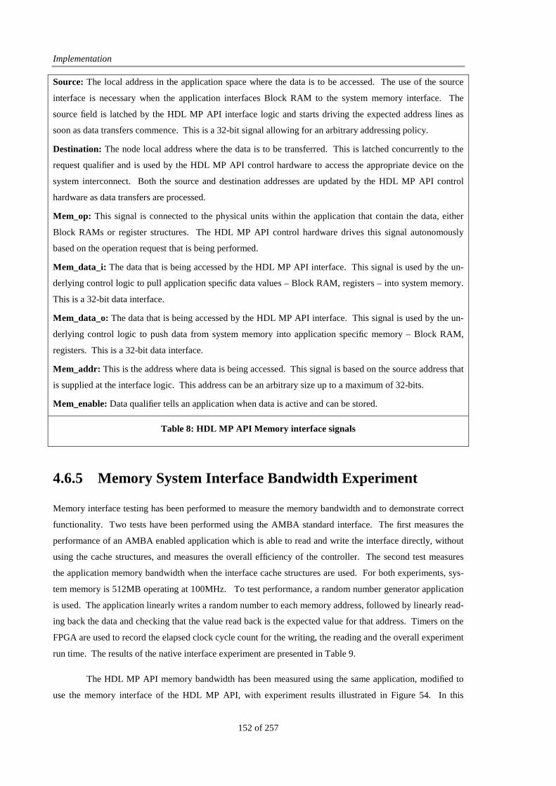
Implementation
152 of 257
Source: The local address in the application space where the data is to be accessed. The use of the source
interface is necessary when the application interfaces Block RAM to the system memory interface. The
source field is latched by the HDL MP API interface logic and starts driving the expected address lines as
soon as data transfers commence. This is a 32-bit signal allowing for an arbitrary addressing policy.
Destination: The node local address where the data is to be transferred. This is latched concurrently to the
request qualifier and is used by the HDL MP API control hardware to access the appropriate device on the
system interconnect. Both the source and destination addresses are updated by the HDL MP API control
hardware as data transfers are processed.
Mem_op: This signal is connected to the physical units within the application that contain the data, either
Block RAMs or register structures. The HDL MP API control hardware drives this signal autonomously
based on the operation request that is being performed.
Mem_data_i: The data that is being accessed by the HDL MP API interface. This signal is used by the un-
derlying control logic to pull application specific data values – Block RAM, registers – into system memory.
This is a 32-bit data interface.
Mem_data_o: The data that is being accessed by the HDL MP API interface. This signal is used by the un-
derlying control logic to push data from system memory into application specific memory – Block RAM,
registers. This is a 32-bit data interface.
Mem_addr: This is the address where data is being accessed. This signal is based on the source address that
is supplied at the interface logic. This address can be an arbitrary size up to a maximum of 32-bits.
Mem_enable: Data qualifier tells an application when data is active and can be stored.
Table 8: HDL MP API Memory interface signals
4.6.5 Memory System Interface Bandwidth Experiment
Memory interface testing has been performed to measure the memory bandwidth and to demonstrate correct
functionality. Two tests have been performed using the AMBA standard interface. The first measures the
performance of an AMBA enabled application which is able to read and write the interface directly, without
using the cache structures, and measures the overall efficiency of the controller. The second test measures
the application memory bandwidth when the interface cache structures are used. For both experiments, sys-
tem memory is 512MB operating at 100MHz. To test performance, a random number generator application
is used. The application linearly writes a random number to each memory address, followed by linearly read-
ing back the data and checking that the value read back is the expected value for that address. Timers on the
FPGA are used to record the elapsed clock cycle count for the writing, the reading and the overall experiment
run time. The results of the native interface experiment are presented in Table 9.
The HDL MP API memory bandwidth has been measured using the same application, modified to
use the memory interface of the HDL MP API, with experiment results illustrated in Figure 54. In this
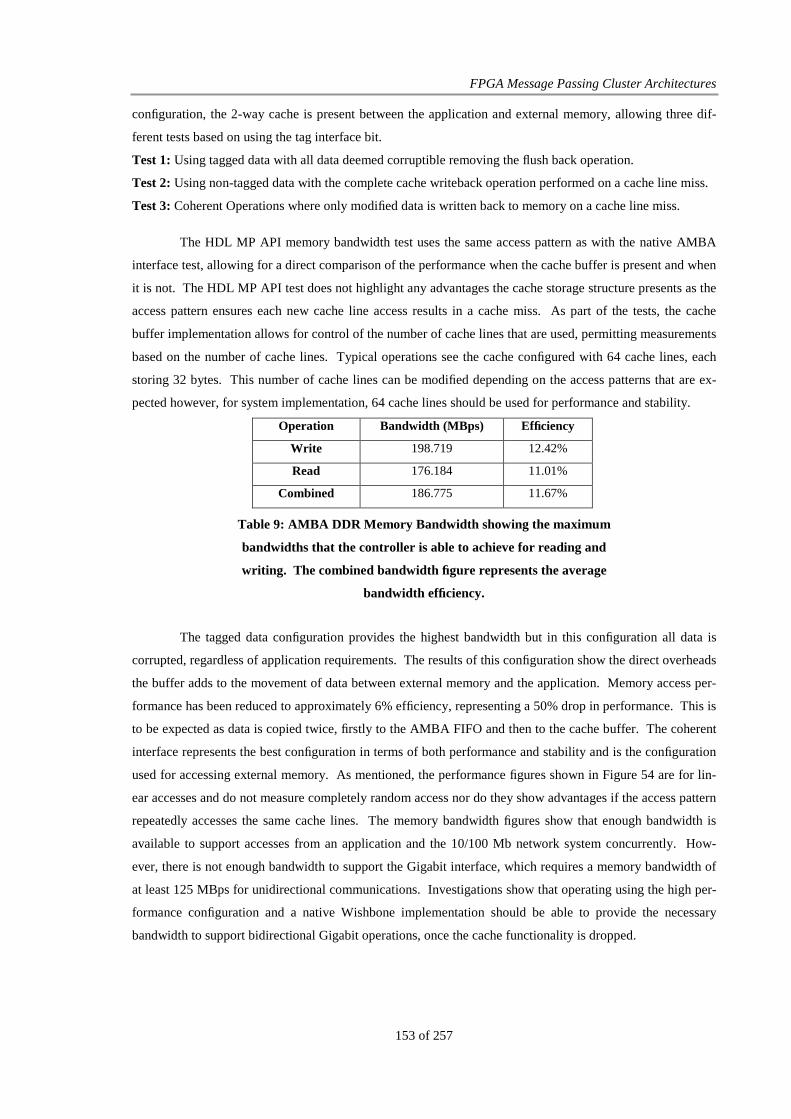
FPGA Message Passing Cluster Architectures
153 of 257
configuration, the 2-way cache is present between the application and external memory, allowing three dif-
ferent tests based on using the tag interface bit.
Test 1: Using tagged data with all data deemed corruptible removing the flush back operation.
Test 2: Using non-tagged data with the complete cache writeback operation performed on a cache line miss.
Test 3: Coherent Operations where only modified data is written back to memory on a cache line miss.
The HDL MP API memory bandwidth test uses the same access pattern as with the native AMBA
interface test, allowing for a direct comparison of the performance when the cache buffer is present and when
it is not. The HDL MP API test does not highlight any advantages the cache storage structure presents as the
access pattern ensures each new cache line access results in a cache miss. As part of the tests, the cache
buffer implementation allows for control of the number of cache lines that are used, permitting measurements
based on the number of cache lines. Typical operations see the cache configured with 64 cache lines, each
storing 32 bytes. This number of cache lines can be modified depending on the access patterns that are ex-
pected however, for system implementation, 64 cache lines should be used for performance and stability.
Operation Bandwidth (MBps) Efficiency
Write 198.719 12.42%
Read 176.184 11.01%
Combined 186.775 11.67%
Table 9: AMBA DDR Memory Bandwidth showing the maximum
bandwidths that the controller is able to achieve for reading and
writing. The combined bandwidth figure represents the average
bandwidth efficiency.
The tagged data configuration provides the highest bandwidth but in this configuration all data is
corrupted, regardless of application requirements. The results of this configuration show the direct overheads
the buffer adds to the movement of data between external memory and the application. Memory access per-
formance has been reduced to approximately 6% efficiency, representing a 50% drop in performance. This is
to be expected as data is copied twice, firstly to the AMBA FIFO and then to the cache buffer. The coherent
interface represents the best configuration in terms of both performance and stability and is the configuration
used for accessing external memory. As mentioned, the performance figures shown in Figure 54 are for lin-
ear accesses and do not measure completely random access nor do they show advantages if the access pattern
repeatedly accesses the same cache lines. The memory bandwidth figures show that enough bandwidth is
available to support accesses from an application and the 10/100 Mb network system concurrently. How-
ever, there is not enough bandwidth to support the Gigabit interface, which requires a memory bandwidth of
at least 125 MBps for unidirectional communications. Investigations show that operating using the high per-
formance configuration and a native Wishbone implementation should be able to provide the necessary
bandwidth to support bidirectional Gigabit operations, once the cache functionality is dropped.
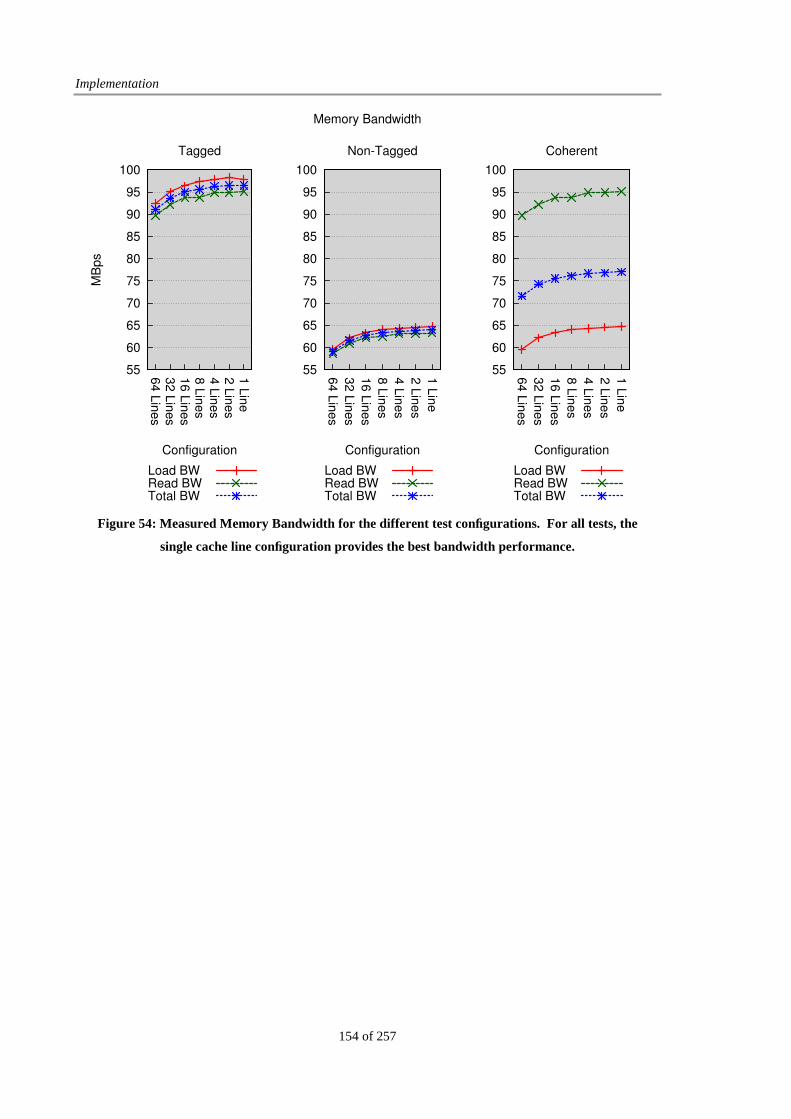
Implementation
154 of 257
Memory Bandwidth
55
60
65
70
75
80
85
90
95
100
64 L
ines
32 L
ines
16 L
ines
8 L
ines
4 L
ines
2 L
ines
1 L
ine
MB
ps
Configuration
Tagged
Load BWRead BWTotal BW
55
60
65
70
75
80
85
90
95
100
64 L
ines
32 L
ines
16 L
ines
8 L
ines
4 L
ines
2 L
ines
1 L
ine
Configuration
Non-Tagged
Load BWRead BWTotal BW
55
60
65
70
75
80
85
90
95
100
64 L
ines
32 L
ines
16 L
ines
8 L
ines
4 L
ines
2 L
ines
1 L
ine
Configuration
Coherent
Load BWRead BWTotal BW
Figure 54: Measured Memory Bandwidth for the different test configurations. For all tests, the
single cache line configuration provides the best bandwidth performance.

155 of 257
Chapter 5
Evaluation
The two experimental architectures, which have been implemented to measure the feasibility of message
passing and switched Ethernet in supporting remote register transfer operations of a distributed hardware
application microarchitecture, have been evaluated through the use of a number of different experiments. A
wide range of experiments have been performed, with the details on what is being measured presented in
Section 3.5. The results of these experiments are presented in this chapter with the results and consequences
from the experiments discussed. As part of the results, the resource usage of each approach can be compared
to say if the one approach is more feasible than the other in terms of the implementation requirements. The
resource usage statistics are those reported by the Xilinx development tools and have been taken from a com-
bination of synthesis and place-and-route reports. For the experiments two different FPGA development
boards have been used. The XUP-V2P [Xilinx '05] development board provides the results for the 100 Mb
Ethernet experiments and consists of a Virtex2Pro30, speed grade -7 and 512 MB 100 MHz DDR RAM.
Xilinx ML402 [Xilinx '06a] development boards were used for the 1000 Mb Ethernet experiments and these
consist of a Virtex4 SX35, speed grade -10.
Different Ethernet switches have been used as part of the experiments to measure the feasibility and
scalability of different approaches to supporting the interconnect between the distributed hardware applica-
tion microarchitectures. The different switches have been obtained as part of preliminary operational testing
and were used to diagnose a range of different problems that arose as part of the implementation. As these
switches were available, they have been used as part of the experiments to show performance differences that
can arise depending on the switch that is used while some generalisations on the results are drawn on the ex-
pected performance for different switch styles. The two main switch styles are managed and unmanaged and
the generalisations will be applied to them as such. The use of different switches demonstrates the operation
of the Ethernet MACs, both the original and the updated architecture, are able to operate in a standards com-
pliant Ethernet network. The use of different switches forms part of the stress test in so far as the Ethernet
controller operations scale to various switches. The following switches have been used for the experiments:
Cisco Catalyst 3548XL: This is a managed store-and-forward switch which would be representative of a
high end 10/100 Mb Ethernet switch.
Evaluation
156 of 257
Netgear FS108: This is an unmanaged store-and-forward switch, representative of a low end 10/100 Mb
Ethernet switch.
Netgear FS508: This is an unmanaged cut-through switch which would be representative of a mid range
10/100 Mb Ethernet switch. Under heavy load conditions, this switch reverts to store-and-forward op-
erations.
Netgear GS608: This is an unmanaged store-and-forward switch which is used to provide the 1000 Mb
Ethernet interconnect. It would be representative of a low end switch.
As part of the operations of each experiment and to demonstrate the fork-join approach to applica-
tion parallelism, the management node is used to load experiment parameters so that the same hardware ap-
plication microarchitecture can be used across a range of values from the number of connected compute units
to the size of data to be used for a remote register transfer. The uploading of experiment parameter data to
the compute units, coupled with an hardware application microarchitecture reset allowed a degree of automa-
tion in the experiments. This allowed for the use of different experiment parameter sizes easily and also
made performing the experiments more straight forward as they could be started without requiring constant
vigilance to ensure they operated correctly. Through the use of the initialisation routine, discussed in Sec-
tions 4.2.1 and 4.3.2, issues with an FPGA node could be easily overcome by using a different FPGA without
requiring a re-synthesis and build of the hardware for the different FPGAs. This ability aided in running the
diverse experiments as not all nodes functioned correctly for a given hardware bit stream. The cause of this
was not discovered as the same hardware bit stream would work faultlessly on one set of experiment nodes
and not on others.
5.1 Stress Test Experiments
The stress test experiments look at how the core components used by the hardware application microarchitec-
ture to perform remote register transfer operations behave. These experiments are concerned that the these
components will support the exchange of data between the various distributed hardware application microar-
chitectures. As part of these experiments, the functionality of the switched Ethernet and the message passing
operations are shown to support data exchange operations. These aspects are tested to show that they are
able to support the exchange of data between interconnected FPGAs while also providing details on how
stably they operate.
5.1.1 Interconnect Stability
Interconnect stability is concerned with measuring how each network switch operates under load. Normal
operations of the FPGA cluster will see random message sizes used for remote register transfer operations.
The majority of packets on the network will be either maximum or minimum sized packets, as Ethernet dis-
plays bimodal data distribution [Shoch '80]. Additional sizes outside the maximum and minimum are tested
to ensure the controller operates correctly across a range of data sizes. The continuous operation and genera-

FPGA Message Passing Cluster Architectures
157 of 257
tion of network packets also places a high degree of stress on the MAC which these experiments look to capi-
talise on to ensure correct operations. This benefits both the dedicated hardware microarchitecture and the
software FPGA processor architectures as the same controller is used by both.
Test Configuration
A two node test configuration is used, with one application microarchitecture acting as a packet producer and
a second acting as a packet consumer. For the experiments, the dedicated hardware architecture is employed
as it is able to produce and insert network packets into the interconnect at a higher rate than the FPGA proc-
essor architecture. The ability to generate packets at a higher rate aids testing the switches under heavier than
expected loads. Different packet sizes are used, with the size of the remote register transfers controlled by
the parameters that are uploaded to the packet producing microarchitecture. This experiment is measuring
the performance of the network under a constant packet stream and to best achieve this, no communication
protocols are employed, rather ready mode register transfers are used. This aids interconnect stress testing
without causing unexpected or unforeseen consequences for the test. As part of the experiment configura-
tion, minor changes were required to the HDL MP API to allow for access to good and bad packet counters.
These changes were not made permanent to the HDL MP API as an application does not require knowledge
of how many error packets have been received. Applications only require to know that the remote register
transfer operation has completed correctly as per the message passing data exchange operations.
Application counters on the FPGAs record relevant experiment information. The producer node
counts the number of packets that are generated while the consumer node counts the number of packets that it
receives, with unique counters present for correct and error packets. Dropped packets are measured as the
difference between all received packets and the number sent. The cause of dropped packets is not investi-
gated as part of the stability test, though congestion or packet errors within a switch will cause dropped pack-
ets. A further counter is present which times the experiment, allowing for control of how long the experi-
ment runs. Each FPGA runs at 100 MHz which was the target timing closure. The resource usage overheads
for the experiment are presented in Table 10. Minor differences were present between the controller used for
the original 100 Mb Ethernet stability testing and the updated 1000 Mb Ethernet controller. Results show
that as the controller has evolved, logic operations and resource usage have been improved.
Slices Flip-Flops LUTs BRAM Frequency
(MHz)
Hardware Base,
Blocking, Virtex2Pro 5,333 (39%) 4,234 (16%) 8,821 (32%) 17 (13%) 81.250
Hardware Base,
Blocking, Virtex4 4,666 (30%) 4,526 (14%) 7,442 (24%) 12 (6%) 129.263
Table 10: Stability Experiment Resource Utilisation
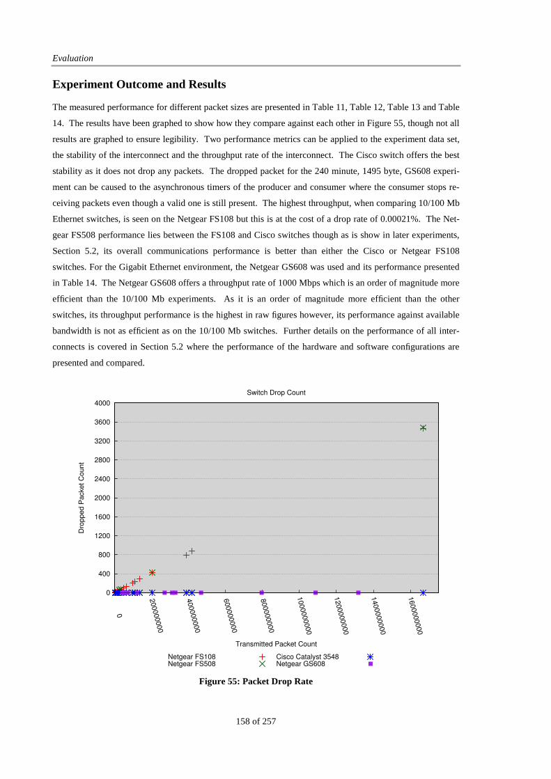
Evaluation
158 of 257
Experiment Outcome and Results
The measured performance for different packet sizes are presented in Table 11, Table 12, Table 13 and Table
14. The results have been graphed to show how they compare against each other in Figure 55, though not all
results are graphed to ensure legibility. Two performance metrics can be applied to the experiment data set,
the stability of the interconnect and the throughput rate of the interconnect. The Cisco switch offers the best
stability as it does not drop any packets. The dropped packet for the 240 minute, 1495 byte, GS608 experi-
ment can be caused to the asynchronous timers of the producer and consumer where the consumer stops re-
ceiving packets even though a valid one is still present. The highest throughput, when comparing 10/100 Mb
Ethernet switches, is seen on the Netgear FS108 but this is at the cost of a drop rate of 0.00021%. The Net-
gear FS508 performance lies between the FS108 and Cisco switches though as is show in later experiments,
Section 5.2, its overall communications performance is better than either the Cisco or Netgear FS108
switches. For the Gigabit Ethernet environment, the Netgear GS608 was used and its performance presented
in Table 14. The Netgear GS608 offers a throughput rate of 1000 Mbps which is an order of magnitude more
efficient than the 10/100 Mb experiments. As it is an order of magnitude more efficient than the other
switches, its throughput performance is the highest in raw figures however, its performance against available
bandwidth is not as efficient as on the 10/100 Mb switches. Further details on the performance of all inter-
connects is covered in Section 5.2 where the performance of the hardware and software configurations are
presented and compared.
0
400
800
1200
1600
2000
2400
2800
3200
3600
4000
0
200000000
400000000
600000000
800000000
1000000000
1200000000
1400000000
1600000000
Dro
pp
ed
Pa
cke
t C
ou
nt
Transmitted Packet Count
Switch Drop Count
Netgear FS108Netgear FS508
Cisco Catalyst 3548Netgear GS608
Figure 55: Packet Drop Rate
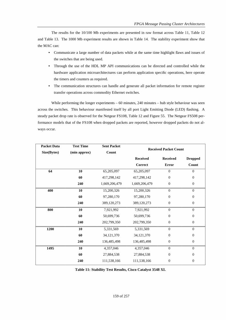
FPGA Message Passing Cluster Architectures
159 of 257
The results for the 10/100 Mb experiments are presented in raw format across Table 11, Table 12
and Table 13. The 1000 Mb experiment results are shown in Table 14. The stability experiment show that
the MAC can:
• Communicate a large number of data packets while at the same time highlight flaws and issues of
the switches that are being used.
• Through the use of the HDL MP API communications can be directed and controlled while the
hardware application microarchitectures can perform application specific operations, here operate
the timers and counters as required.
• The communication structures can handle and generate all packet information for remote register
transfer operations across commodity Ethernet switches.
While performing the longer experiments – 60 minutes, 240 minutes – hub style behaviour was seen
across the switches. This behaviour manifested itself by all port Light Emitting Diode (LED) flashing. A
steady packet drop rate is observed for the Netgear FS108, Table 12 and Figure 55. The Netgear FS508 per-
formance models that of the FS108 when dropped packets are reported, however dropped packets do not al-
ways occur.
Packet Data
Size(Bytes)
Test Time
(min approx)
Sent Packet
Count Received Packet Count
Received
Correct
Received
Error
Dropped
Count
64 10 65,205,097 65,205,097 0 0
60 417,298,142 417,298,142 0 0
240 1,669,206,479 1,669,206,479 0 0
400 10 15,200,326 15,200,326 0 0
60 97,280,170 97,280,170 0 0
240 389,120,273 389,120,273 0 0
800 10 7,921,992 7,921,992 0 0
60 50,699,736 50,699,736 0 0
240 202,799,350 202,799,350 0 0
1200 10 5,331,569 5,331,569 0 0
60 34,121,370 34,121,370 0 0
240 136,485,498 136,485,498 0 0
1495 10 4,357,046 4,357,046 0 0
60 27,884,538 27,884,538 0 0
240 111,538,166 111,538,166 0 0
Table 11: Stability Test Results, Cisco Catalyst 3548 XL
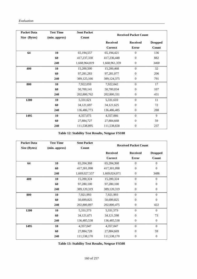
Evaluation
160 of 257
Packet Data
Size (Bytes)
Test Time
(min. approx)
Sent Packet
Count Received Packet Count
Received
Correct
Received
Error
Dropped
Count
64 10 65,194,557 65,194,421 0 136
60 417,237,330 417,236,448 0 882
240 1,668,964,819 1,668,961,359 0 3460
400 10 15,200,500 15,200,468 0 32
60 97,281,283 97,281,077 0 206
240 389,125,166 389,124,375 0 791
800 10 7,922,059 7,922,042 0 17
60 50,700,141 50,700,034 0 107
240 202,800,762 202,800,331 0 431
1200 10 5,331,621 5,331,610 0 11
60 34,121,697 34,121,625 0 72
240 136,486,773 136,486,485 0 288
1495 10 4,357,075 4,357,066 0 9
60 27,884,727 27,884,668 0 59
240 111,538,895 111,538,658 0 237
Table 12: Stability Test Results, Netgear FS108
Packet Data
Size (Bytes)
Test Time
(min. approx)
Sent Packet
Count Received Packet Count
Received
Correct
Received
Error
Dropped
Count
64 10 65,204,368 65,204,368 0 0
60 417,301,098 417,301,098 0 0
240 1,669,027,557 1,669,024,071 0 3486
400 10 15,200,324 15,200,324 0 0
60 97,280,100 97,280,100 0 0
240 389,120,319 389,120,319 0 0
800 10 7,921,993 7,921,993 0 0
60 50,699,825 50,699,825 0 0
240 202,800,897 202,800,475 0 422
1200 10 5,331,573 5,331,573 0 0
60 34,121,671 34,121,598 0 73
240 136,485,538 136,485,538 0 0
1495 10 4,357,047 4,357,047 0 0
60 27,884,728 27,884,669 0 59
240 111,538,170 111,538,170 0 0
Table 13: Stability Test Results, Netgear FS508
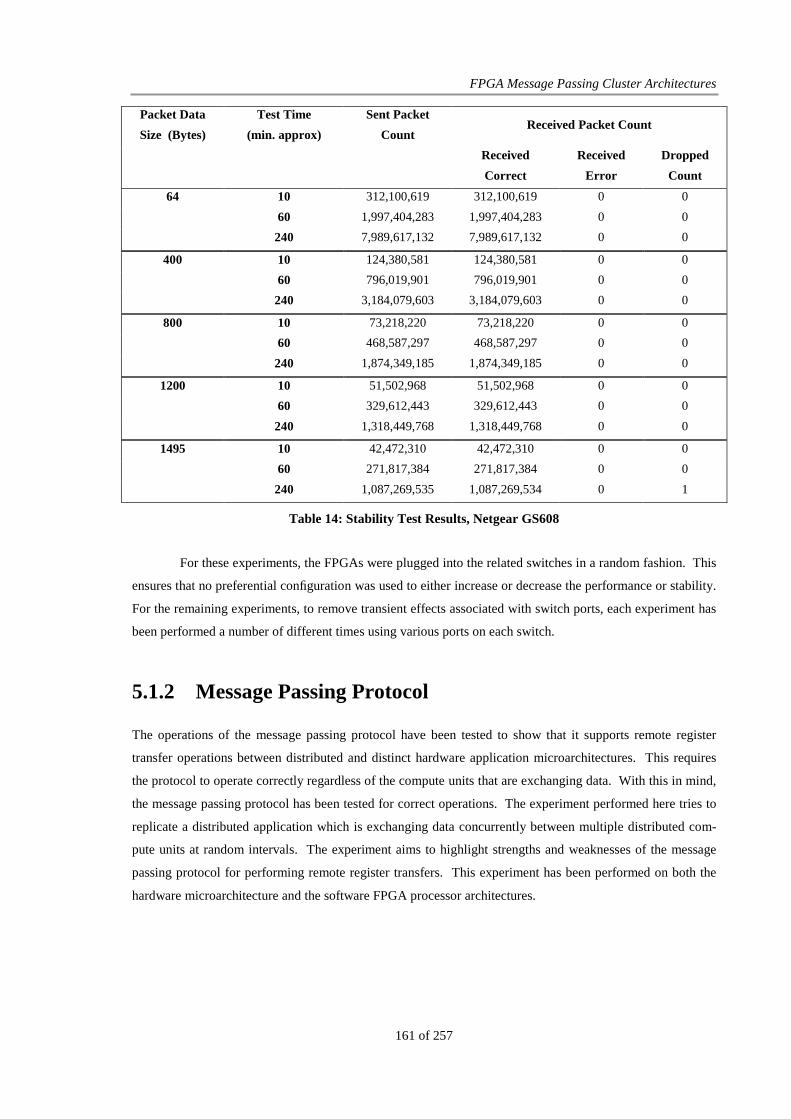
FPGA Message Passing Cluster Architectures
161 of 257
Packet Data
Size (Bytes)
Test Time
(min. approx)
Sent Packet
Count Received Packet Count
Received
Correct
Received
Error
Dropped
Count
64 10 312,100,619 312,100,619 0 0
60 1,997,404,283 1,997,404,283 0 0
240 7,989,617,132 7,989,617,132 0 0
400 10 124,380,581 124,380,581 0 0
60 796,019,901 796,019,901 0 0
240 3,184,079,603 3,184,079,603 0 0
800 10 73,218,220 73,218,220 0 0
60 468,587,297 468,587,297 0 0
240 1,874,349,185 1,874,349,185 0 0
1200 10 51,502,968 51,502,968 0 0
60 329,612,443 329,612,443 0 0
240 1,318,449,768 1,318,449,768 0 0
1495 10 42,472,310 42,472,310 0 0
60 271,817,384 271,817,384 0 0
240 1,087,269,535 1,087,269,534 0 1
Table 14: Stability Test Results, Netgear GS608
For these experiments, the FPGAs were plugged into the related switches in a random fashion. This
ensures that no preferential configuration was used to either increase or decrease the performance or stability.
For the remaining experiments, to remove transient effects associated with switch ports, each experiment has
been performed a number of different times using various ports on each switch.
5.1.2 Message Passing Protocol
The operations of the message passing protocol have been tested to show that it supports remote register
transfer operations between distributed and distinct hardware application microarchitectures. This requires
the protocol to operate correctly regardless of the compute units that are exchanging data. With this in mind,
the message passing protocol has been tested for correct operations. The experiment performed here tries to
replicate a distributed application which is exchanging data concurrently between multiple distributed com-
pute units at random intervals. The experiment aims to highlight strengths and weaknesses of the message
passing protocol for performing remote register transfers. This experiment has been performed on both the
hardware microarchitecture and the software FPGA processor architectures.

Evaluation
162 of 257
Test Configuration
To test the message passing protocol operations, multiple nodes are used. The more nodes that can be used,
the more robustly the protocol can be tested. The experiment consists of multiple nodes, each configured to
perform remote register transfer operations with another hardware application microarchitecture. To ensure a
better test of the protocol, the microarchitecture running on each compute unit is configured to perform ran-
domised communications between the different units. A timer is used to perform the randomisation for start-
ing the remote register transfer operations between microarchitectures. The randomised time between remote
register transfer operations is based on the compute unit identity number and the unit that the exchange is
occurring with. The randomised timer is used to reflect a real system where the timing of a communication
will not be at the same for all compute units.
Remote register transfer order between the compute units is known in advance so the testing of the
message passing communication ensures the system is able to handle packets which may not arrive when
expected. The order is known in advance as a correctly functioning message passing implementation must be
used across the system, otherwise the communication between nodes would not function correctly. This is-
sue is independent of the message passing and communication protocol operations that are performed on the
network.
Experiment Outcome and Results
The protocol experiment investigates the remote register transfer operations using the message passing proto-
col across a range of data sizes between different numbers of distributed hardware microarchitectures. As the
aim is to ensure the correct exchange of data, the performance metric of interest is that the remote register
transfer operation has completed correctly between the microarchitectures. To measure this, the node appli-
cation is required to inform the software head node that they have completed the exchange of the data across
the cluster and the time it has taken to perform this. The latter figure is a measure of how long it has taken
however with the randomised time between communications, the value does not represent a performance
measurement for the cluster.
Different message exchange sizes are used to again better target real applications and how they will
behave and operate on the cluster. Correct operations of the message passing protocol were seen across the
FPGA cluster in a three compute unit configuration. Message passing protocol testing on larger numbers of
nodes were not undertaken using this experiment configuration however, testing of the barrier and initialisa-
tion routines using higher node counts show the message passing protocol scales to higher numbers of nodes,
Sections 5.3.1 and 5.3.2.
5.1.3 Stress Testing Discussion
The stress tests have looked at the two main aspects of the switched Ethernet implementation of the FPGA

FPGA Message Passing Cluster Architectures
163 of 257
cluster, the physical communication medium and the message passing protocols operations in supporting the
exchange of data between distributed application logic. Preliminary observations on the results show that for
the physical interconnect, the following generalisations about the switches can be made. From the results
presented in one-way communication, the managed switch provides the best overall performance as it allows
for the highest packet throughput across most experiment sizes while also providing the greatest stability in
terms of no dropped packets. This coupled with additional features of the managed switch which supported
testing make it an ideal choice for the interconnect between FPGAs
The message passing protocol experiments look at how the protocol operates between the distrib-
uted hardware application architectures, showing that the message passing protocol that has been designed
and implemented is able to support the exchange of data between hardware application microarchitectures
independently of the communication mechanism that is used – hardware or software, managed or unmanaged
switches. The results of the message passing protocol experiment give confidence that the use of a switched
Ethernet interconnect is a viable platform for supporting application distribution across many interconnected
FPGAs. The stress tests have shown that the components are able to support the remote register transfer op-
erations of distributed hardware application microarchitectures through the use of the HDL MP API.
5.2 Benchmark Experiments
Benchmark experiments have been developed to look at the performance of the hardware and software ap-
proaches for performing a range of remote register transfer operations using the HDL MP API as the means
to exchange data. Unless otherwise discussed, the use of synchronous, flow controlled remote register trans-
fers can be assumed. The performance metrics of interest are the time it takes to exchange data between
compute units – Latency – and the efficiency of the exchange of data between compute units – Bandwidth.
Two distinct bandwidth experiments have been performed, the first measuring direct Block RAM to Block
RAM remote register transfers and the second measuring the maximum bandwidth that is achievable when
more arbitrary data exchange sizes are requested. As part of the second bandwidth experiment, enough
memory is assumed to be available to measure the different remote register transfer sizes. The bandwidth
experiments are performed between two compute units.
5.2.1 Latency
Latency is the measure of the minimum time required to exchange a zero sized message between two com-
municating compute units. Communication latency is measured using a standard ping-pong message ex-
change. The ping-pong experiment measures the time taken to exchange a set amount of minimum sized
packets between two connected compute units. This test configuration measures both one-way and round-
trip latency times, with a one-way trip time half that of the round-trip time.

Evaluation
164 of 257
Test Configuration
To measure the communication latency, two interconnected HDL MP API enabled hardware application mi-
croarchitectures, using the various validation switches presented previously, perform a minimum sized re-
mote register transfer. To remove transient effects that the connection ports and internal switch topology can
introduce, the experiments were run using different ports on each switch. The average results of the given
experiment across the different ports are presented in the associated graphs.
The hardware application microarchitectures’ exchange zero sized messages. Design considerations
mean a minimum application requested size of 1 byte must be used. However, this does not influence latency
measurements as a minimum packet size of 64 bytes is required by Ethernet – 46 bytes data. Hardware ap-
plication timers record the experiment elapsed clock cycle count. The timers record the elapsed time from
the first remote register transfer until the final transfer is complete. Unidirectional communications are per-
formed between the hardware application microarchitectures meaning one node is sending the message data
while the other node is receiving the message data. When flow control is used, both nodes will be sending
and receiving data as per the communication protocol. Latency is the elapsed time for the individual ex-
change of data between the nodes. The application counters record the round-trip elapsed time. The latency
time for one-way communication is half that of the round-trip time.
Experiment parameters are uploaded to each hardware application microarchitecture before the ex-
periment is started. Upon receiving the experiment parameters, the first remote register transfer operation
commences while the experiment counters begin recording the elapsed experiment time. Once the last re-
mote register transfer operation has completed, the counters are stopped. As well as measuring the latency
across the various experiment switches, investigations into point-to-point latency were also performed,
through the use of a cross-over cable between the two compute units. This configuration is only useful for
reference as the implementation of the architectures uses switches to support scalability of the available com-
pute resources for different algorithms. To ensure an accurate measure of network latency, each latency ex-
periment was performed a minimum of 1,000 times with most results reported having been run 10,000 times.
No statistically significant difference was seen between either experiment size. During experiment develop-
ment, the ability to enable and disable network communication flow control was also investigated. Four
separate ping-pong latency tests have been performed, as part of the latency experiment. Test classification is
based on the communication mode and flow control strategy.
Test 1: Measures the minimum latency of the switches by looking at the time to exchange only raw data be-
tween the nodes. For this test, no message passing or communication protocols are employed. This test
gives the lower bound on the communication overheads through the various switches.
Test 2: Measures the latency of the communication protocol by looking at the cost added by the communica-
tion protocol acknowledgement operations. Differences that are reported between test 1 and 2, show the
additional processing that is needed for the communications protocol.
Test 3: Measures the overhead that the message passing protocol adds. The synchronise overheads are meas-
ured in this test. This test highlights introduced switch overheads as the hand shake message passing op-
eration requires multiple switch passes.

FPGA Message Passing Cluster Architectures
165 of 257
Test 4: Measures the end to end time that can be expected at the HDL MP API interface for performing a
remote register transfer operation. This test uses both the message passing and communication protocols
to look at the latency of the HDL MP API interface under normal loads.
Synchronisation Flow Control
Test 1 � � Test 2 � � Test 3 � � Test 4 � �
Table 15: Latency Experiment communication components
As part of the latency experiment, the frequency of the dedicated hardware microarchitecture has
been modified. A target frequency of 100 MHz is used for all experiments but as part of the latency tests, the
hardware was modified to use 75 MHz and 55 MHz. This measures the cross-clock domain operations of the
network controller while also measuring the HDL MP API functionality with different frequencies. This
latter aspect is useful, as it shows that a distributed hardware application microarchitecture does not have to
function at 100 MHz. The slower clock frequency applications have only been measured for the 10/100 Mb
Ethernet switched network to show that the core application frequency can be controlled. Similar experi-
ments on the software and the 1000 Mb Ethernet hardware have not been performed as the synthesis reports
for this show a large differential between the network frequencies and the base target frequency of 100 MHz.
For the experiments, a combination of Block RAMs and application registers are used to store the
data. As a minimum amount of data is being sent, 1 byte of actual data, the majority of the data moving
across the network will be padded Ethernet packets, which are automatically added by the MAC.
Slices Flip-Flops LUTs BRAM Frequency
(MHz) Application Code
Size (Bytes)
Hardware,
No Flow Control,
Test 1, 3
4,394 3,455 7,198 12 106.760 N/A
Hardware,
Flow Control, Test 2, 4
4,695 3,912 7,564 12 108.288 N/A
FPGA Processor,
No Flow Control,
Test 1, 3
5,442 5,217 8,196 31 107.984 12,396
FPGA Processor,
Flow Control,
Test 2, 4
5,442 5,217 8,196 31 107.984 12,396
Table 16: Latency Experiment Resource Utilisation

Evaluation
166 of 257
Experiment Outcome and Results
The experiment results are collated based on switch, and are shown in Figure 56 to Figure 60. Results pres-
entation based on data collation allows for a direct comparison of the two architectures across that switch.
To directly compare the performance across the switches, the measured test results are given in Table 17.
The differences between the experiment tests show which aspect of the two protocols adds the largest over-
head to the correct operation of the FPGA cluster nodes e.g. the on node processing, the interconnection
switch etc. This is seen by the proportional result differences between the two platforms. The hardware
shows a marked performance boost of between 20% and 30% across all sizes for the 10/100 Mb Ethernet
switch. For the 1000 Mb Ethernet switch, the hardware shows between 250% and 350% improvement in
performance against the FPGA processor architecture.
For test 1 and test 2, very little protocol processing is performed. In test 1, the remote register trans-
fer operation sees the exchange of application only data. No testing is performed on the data, rather the
overheads of performing the remote register transfer are measured. The hardware architecture is able to
transfer the data directly into the hardware application microarchitecture registers while the software FPGA
processor architecture must wait for the packet to be completely received before moving it to the application.
As a message exchange of 1 byte is used, very little data exchanging is performed. The FPGA processor
architecture experiments show the overheads that are going to be present for moving data between the net-
work and the application, with an overhead of approximately 5 µs recorded for the latency experiment. This
time matches the expected time to receive a minimum sized packet. Test 2, under correct operations, will
transfer two packets for the experiment. The first packet is the data, the second packet the acknowledgement.
To generate the acknowledgement and to ensure the communication is operating correctly, the message pass-
ing and communication protocols must be used to test the data before it is transferred to the application regis-
ters. This processing ensures that the packet has been received correctly and the necessary communication
protocol response is generated – acknowledgement or negative acknowledgement. The experiment configu-
ration is such that once the HDL MP API informs the hardware application microarchitecture that the com-
munication is complete, the next communication operation is performed. Latency between test 1 and 2 does
not increase linearly as the movement of data is overlapped between the acknowledgement and the next re-
mote register transfer operation. Once the acknowledgement is generated, that node has completed its mes-
sage passing operations and moves onto the next remote register transfer operation. As this is a remote regis-
ter send, it is able to send the data immediately following the acknowledgement packet on the interconnect.
Test 3 synchronises the nodes before performing the remote register transfer operation. For correct
operation, three packets are required. The synchronisation exchange removes the overlapping communica-
tions as no data is exchanged between compute units until the two message passing protocol state machines
are synchronised for the remote register transfer operation. As the majority of the communications can not
be overlapped, the latency of the switch plays a large part in the performance of both the hardware and FPGA
processor architectures. The dedicated hardware architecture is able to test the network packets as they arrive
at the network interface, reducing the packet processing overheads while the FPGA processor must wait for
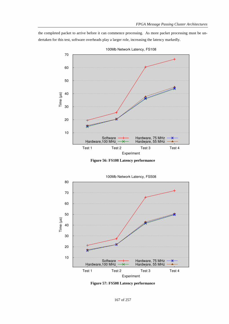
FPGA Message Passing Cluster Architectures
167 of 257
the completed packet to arrive before it can commence processing. As more packet processing must be un-
dertaken for this test, software overheads play a larger role, increasing the latency markedly.
10
20
30
40
50
60
70
Test 1 Test 2 Test 3 Test 4
Tim
e (
µs)
Experiment
100Mb Network Latency, FS108
SoftwareHardware,100 MHz
Hardware, 75 MHzHardware, 55 MHz
Figure 56: FS108 Latency performance
10
20
30
40
50
60
70
80
Test 1 Test 2 Test 3 Test 4
Tim
e (
µs)
Experiment
100Mb Network Latency, FS508
SoftwareHardware,100 MHz
Hardware, 75 MHzHardware, 55 MHz
Figure 57: FS508 Latency performance
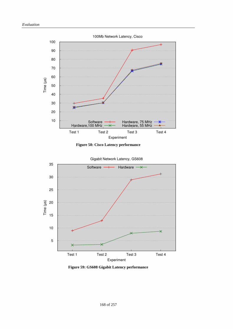
Evaluation
168 of 257
10
20
30
40
50
60
70
80
90
100
Test 1 Test 2 Test 3 Test 4
Tim
e (
µs)
Experiment
100Mb Network Latency, Cisco
SoftwareHardware,100 MHz
Hardware, 75 MHzHardware, 55 MHz
Figure 58: Cisco Latency performance
5
10
15
20
25
30
35
Test 1 Test 2 Test 3 Test 4
Tim
e (
µs)
Experiment
Gigabit Network Latency, GS608
Software Hardware
Figure 59: GS608 Gigabit Latency performance

FPGA Message Passing Cluster Architectures
169 of 257
5
10
15
20
25
30
35
40
45
50
Test 1 Test 2 Test 3 Test 4
Tim
e (
µs)
Experiment
100Mb Network Latency, Cross Over
Software Hardware
Figure 60: Crossover latency performance
Test 4 reflects the expected operations and behaviour of a remote register transfer at all times, the
compute units synchronise before performing the remote register transfer, followed with the acknowledge-
ment of the transferred data. Test 4 reflects the latency that will be seen at the HDL MP API by the hard-
ware application microarchitecture. As with tests 1 and 2, no large performance difference is seen between
test 3 and 4 as again, the synchronisation packet is transmitted directly following the acknowledgement
packet so overlapping the operations further. As both packets are traversing the network at the same time,
very little additional overhead, above the node processing occurs. The results shown in Figure 60, Crossover
interconnect, reflect the latency when no intermediary switches are present between the compute units.
The time taken across these experiments, reflect the minimum amount of processing time that is re-
quired by the network layers and network structures for the remote register transfer operation. The time to
transmit a minimum sized packet on Ethernet, 46 bytes at 25 MHz is 5.76 µs. From the results of Test 1, this
shows a hardware FPGA overhead latency of 1.79 µs for the processing and moving of the data, using the
numeric information from Table 17. For the FPGA processor experiment, an overhead of 7 µs is seen for the
movement of the raw data, showing the expected times for moving data to the network buffer and processor
access overheads. These figures are in contrast to the switch based results, where the overhead of the switch
exceeds the processing overheads of each architecture. From the above figures, for the FPGA processor a 7
µs overhead is larger than that for the crossover communication time while, for the switch based systems, it is
less than 50% of the time required to move the data across the switch.
Each switch has a different latency that is reported as part of the switch specification. The Cisco
switch has the highest latency, which can be attributed to the management operations that it performs. The
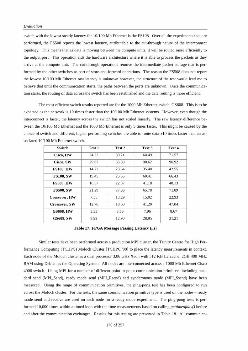
Evaluation
170 of 257
switch with the lowest steady latency for 10/100 Mb Ethernet is the FS108. Over all the experiments that are
performed, the FS508 reports the lowest latency, attributable to the cut-through nature of the interconnect
topology. This means that as data is moving between the compute units, it will be routed more efficiently to
the output port. This operation aids the hardware architecture where it is able to process the packets as they
arrive at the compute unit. The cut-through operations remove the intermediate packet storage that is per-
formed by the other switches as part of store-and-forward operations. The reason the FS508 does not report
the lowest 10/100 Mb Ethernet raw latency is unknown however, the structure of the test would lead me to
believe that until the communication starts, the paths between the ports are unknown. Once the communica-
tion starts, the routing of data across the switch has been established and the data routing is more efficient.
The most efficient switch results reported are for the 1000 Mb Ethernet switch, GS608. This is to be
expected as the network is 10 times faster than the 10/100 Mb Ethernet systems. However, even though the
interconnect is faster, the latency across the switch has not scaled linearly. The raw latency difference be-
tween the 10/100 Mb Ethernet and the 1000 Mb Ethernet is only 5 times faster. This might be caused by the
choice of switch and different, higher performing switches are able to route data x10 times faster than an as-
sociated 10/100 Mb Ethernet switch.
Switch Test 1 Test 2 Test 3 Test 4
Cisco, HW 24.32 30.21 64.49 71.57
Cisco, SW 29.67 35.59 90.62 96.92
FS108, HW 14.72 23.64 35.48 42.55
FS108, SW 19.45 25.55 60.41 66.43
FS508, HW 16.57 22.37 41.18 48.13
FS508, SW 21.29 27.36 65.78 71.89
Crossover, HW 7.55 13.29 15.02 22.93
Crossover, SW 12.76 18.60 41.20 47.04
GS608, HW 3.33 3.53 7.96 8.67
GS608, SW 8.99 12.90 28.95 31.21
Table 17: FPGA Message Passing Latency (µs)
Similar tests have been performed across a production MPI cluster, the Trinity Centre for High Per-
formance Computing (TCHPC) Moloch Cluster [TCHPC '08] to place the latency measurements in context.
Each node of the Moloch cluster is a dual processor 3.06 GHz Xeon with 512 KB L2 cache, 2GB 400 MHz
RAM using Debian as the Operating System. All nodes are interconnected across a 1000 Mb Ethernet Cisco
4006 switch. Using MPI for a number of different point-to-point communication primitives including stan-
dard send (MPI_Send), ready mode send (MPI_Rsend) and synchronous mode (MPI_Ssend) have been
measured. Using the range of communication primitives, the ping-pong test has been configured to run
across the Moloch cluster. For the tests, the same communication primitive type is used on the nodes – ready
mode send and receive are used on each node for a ready mode experiment. The ping-pong tests is per-
formed 10,000 times within a timed loop with the time measurements based on calling gettimeofday() before
and after the communication exchanges. Results for this testing are presented in Table 18. All communica-
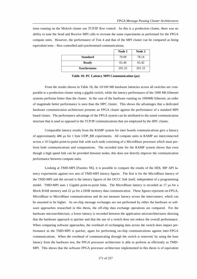
FPGA Message Passing Cluster Architectures
171 of 257
tions running on the Moloch cluster use TCP/IP flow control. As this is a production cluster, there was no
ability to tune the Send and Receive MPI calls to recreate the same experiments as performed for the FPGA
compute units. However, the performance of Test 4 and that of the MPI cluster can be compared as being
equivalent tests – flow controlled and synchronised communications.
Node 1 Node 2
Standard 70.09 78.14
Ready 65.46 65.42
Synchronous 201.32 201.33
Table 18: PC Latency MPI Communication (µs)
From the results shown in Table 18, the 10/100 Mb hardware latencies across all switches are com-
parable to a production cluster using a gigabit switch, while the latency performance of the 1000 Mb Ethernet
systems performs better than the cluster. In the case of the hardware running on 1000Mb Ethernet, an order
of magnitude better performance is seen than the HPC cluster. This shows the advantages that a dedicated
hardware communication architecture presents an FPGA cluster against the performance of a standard MPI
based cluster. The performance advantage of the FPGA system can be attributed to the tuned communication
structure that is used as opposed to the TCP/IP communications that are employed by the HPC cluster.
Comparable latency results from the RAMP system for inter boards communications give a latency
of approximately 486 µs for 1 byte UDP_RR experiments. All compute units in RAMP are interconnected
across a 10 Gigabit point-to-point link with each node consisting of a MicroBlaze processor which must per-
form both communications and computations. The recorded time for the RAMP system shows that even
though a high speed link can be provided between nodes, this does not directly improve the communication
performance between compute units.
Looking at TMD-MPI [Fuentes '06], it is possible to compare the results of the HDL MP API la-
tency experiments against two sets of TMD-MPI latency figures. The first is for the MicroBlaze latency of
the TMD-MPI and the second is the latency figures of the OCCC link itself, independent of a programming
model. TMD-MPI uses 1 Gigabit point-to-point links. The MicroBlaze latency is recorded as 17 µs for a
Block RAM memory and 22 µs for a DDR memory data communication. These figures represent on-FPGA,
MicroBlaze to MicroBlaze communications and do not measure latency across the interconnect, which can
be assumed to be higher. As on-chip message exchanges are not performed by either the hardware or soft-
ware approaches researched in this thesis, the off-chip data exchange operations are compared. For the
hardware microarchitecture, a lower latency is recorded between the application microarchitectures showing
that the hardware approach is quicker and that the use of a switch does not reduce the overall performance.
When comparing software approaches, the overhead of exchanging data across the switch does impact per-
formance as the TMD-MPI is quicker, again for performing on-chip communications against inter-FPGA
communications. When the overhead of communicating through the switch is removed, by using the base
latency from the hardware test, the FPGA processor architecture is able to perform as efficiently as TMD-
MPI. This shows that the software FPGA processor architecture implemented in this thesis is of equivalent

Evaluation
172 of 257
performance to the TMD-MPI system while operating across commodity Ethernet switches. This demon-
strates a performance advantage and implementation difference between the TMD-MPI and the approach in
this work. From looking at the TMD-MPI, the main area that impacts performance is the reduced operational
clock frequency, caused by wanting reasonable implementation turnaround times. For TMD-MPI, approxi-
mately 680 processor cycles are needed to exchanging data while, for HDL MP API, approximately 3,000
processor cycles are needed, including the time to exchange data across the switch. So while performance
are equivalent between the two, if the store-and-forward overheads of the switch are removed, the operational
frequency accounts for the majority of the performance difference. As this is caused by wanting a reduced
implementation overhead for TMD-MPI, caused by static node identity generation, the use of a dynamic ap-
proach as part of this thesis shows a performance advantage in increased operational frequency.
The OCCC system reports a latency of 1.23 µs. The hardware architecture used in this thesis
achieves similar performance again, once the store-and-forward overheads of the switches are taken into ac-
count, when compared with possible point-to-point connections. While the switch is a requirement of this
thesis, the reduced latency of the MGT point-to-point approaches does present an advantage for their use
with applications that are latency sensitive against applications which requiring scalability over latency.
5.2.2 Block RAM Message Passing Exchange
Block RAMs are used to store application data to improve the computational performance as seen with EP
and MG computations where many Block RAMs are used for temporary storage. This can frequently be data
that needs to be exchanged between the distributed hardware elements that make up the FPGA cluster, e.g.
edge boundary data in MG computations. As the Block RAM registers store the information needed in a
remote register transfer operation, the overheads of exchanging this data is measured. For the Block RAM
message passing exchange, the time to exchange data between compute units using the HDL MP API to ac-
cess and transfer the data in the application Block RAMs is measured. Results from this experiment will
benefit observations on the amount of parallelism that will be required on each FPGA to ensure the commu-
nication does not become a bottleneck.
Test Configuration
The purpose of this experiment is to exchange a defined amount of data based on the size of FPGA Block
RAMs. To achieve this, different Block RAM sizes have be connected to the HDL MP API based on the size
of the remote register transfer operation that is expected. The data sizes used for the Block RAMs reflect
sizes that an application may use, independently of how the interconnect performs on those sizes i.e. the size
of the Block RAM which works best for an application may not work well with the network MTU. For this
experiment, two distributed hardware application microarchitectures are interconnected and the time to per-
form the remote register transfer operations are measured.
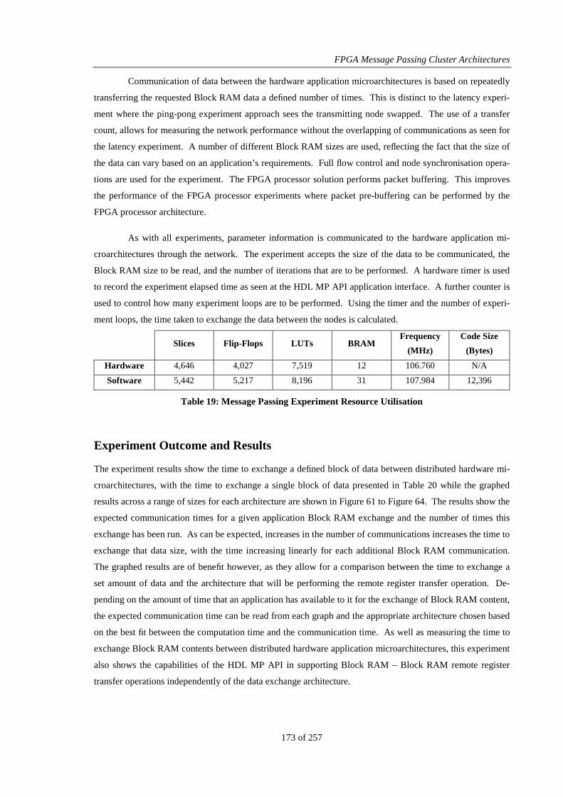
FPGA Message Passing Cluster Architectures
173 of 257
Communication of data between the hardware application microarchitectures is based on repeatedly
transferring the requested Block RAM data a defined number of times. This is distinct to the latency experi-
ment where the ping-pong experiment approach sees the transmitting node swapped. The use of a transfer
count, allows for measuring the network performance without the overlapping of communications as seen for
the latency experiment. A number of different Block RAM sizes are used, reflecting the fact that the size of
the data can vary based on an application’s requirements. Full flow control and node synchronisation opera-
tions are used for the experiment. The FPGA processor solution performs packet buffering. This improves
the performance of the FPGA processor experiments where packet pre-buffering can be performed by the
FPGA processor architecture.
As with all experiments, parameter information is communicated to the hardware application mi-
croarchitectures through the network. The experiment accepts the size of the data to be communicated, the
Block RAM size to be read, and the number of iterations that are to be performed. A hardware timer is used
to record the experiment elapsed time as seen at the HDL MP API application interface. A further counter is
used to control how many experiment loops are to be performed. Using the timer and the number of experi-
ment loops, the time taken to exchange the data between the nodes is calculated.
Slices Flip-Flops LUTs BRAM Frequency
(MHz)
Code Size
(Bytes)
Hardware 4,646 4,027 7,519 12 106.760 N/A
Software 5,442 5,217 8,196 31 107.984 12,396
Table 19: Message Passing Experiment Resource Utilisation
Experiment Outcome and Results
The experiment results show the time to exchange a defined block of data between distributed hardware mi-
croarchitectures, with the time to exchange a single block of data presented in Table 20 while the graphed
results across a range of sizes for each architecture are shown in Figure 61 to Figure 64. The results show the
expected communication times for a given application Block RAM exchange and the number of times this
exchange has been run. As can be expected, increases in the number of communications increases the time to
exchange that data size, with the time increasing linearly for each additional Block RAM communication.
The graphed results are of benefit however, as they allow for a comparison between the time to exchange a
set amount of data and the architecture that will be performing the remote register transfer operation. De-
pending on the amount of time that an application has available to it for the exchange of Block RAM content,
the expected communication time can be read from each graph and the appropriate architecture chosen based
on the best fit between the computation time and the communication time. As well as measuring the time to
exchange Block RAM contents between distributed hardware application microarchitectures, this experiment
also shows the capabilities of the HDL MP API in supporting Block RAM – Block RAM remote register
transfer operations independently of the data exchange architecture.
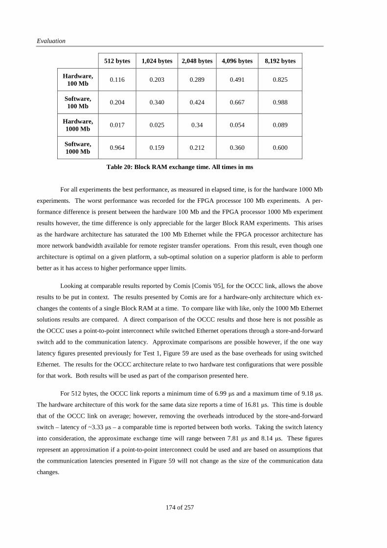
Evaluation
174 of 257
512 bytes 1,024 bytes 2,048 bytes 4,096 bytes 8,192 bytes
Hardware, 100 Mb
0.116 0.203 0.289 0.491 0.825
Software, 100 Mb
0.204 0.340 0.424 0.667 0.988
Hardware, 1000 Mb
0.017 0.025 0.34 0.054 0.089
Software, 1000 Mb
0.964 0.159 0.212 0.360 0.600
Table 20: Block RAM exchange time. All times in ms
For all experiments the best performance, as measured in elapsed time, is for the hardware 1000 Mb
experiments. The worst performance was recorded for the FPGA processor 100 Mb experiments. A per-
formance difference is present between the hardware 100 Mb and the FPGA processor 1000 Mb experiment
results however, the time difference is only appreciable for the larger Block RAM experiments. This arises
as the hardware architecture has saturated the 100 Mb Ethernet while the FPGA processor architecture has
more network bandwidth available for remote register transfer operations. From this result, even though one
architecture is optimal on a given platform, a sub-optimal solution on a superior platform is able to perform
better as it has access to higher performance upper limits.
Looking at comparable results reported by Comis [Comis '05], for the OCCC link, allows the above
results to be put in context. The results presented by Comis are for a hardware-only architecture which ex-
changes the contents of a single Block RAM at a time. To compare like with like, only the 1000 Mb Ethernet
solutions results are compared. A direct comparison of the OCCC results and those here is not possible as
the OCCC uses a point-to-point interconnect while switched Ethernet operations through a store-and-forward
switch add to the communication latency. Approximate comparisons are possible however, if the one way
latency figures presented previously for Test 1, Figure 59 are used as the base overheads for using switched
Ethernet. The results for the OCCC architecture relate to two hardware test configurations that were possible
for that work. Both results will be used as part of the comparison presented here.
For 512 bytes, the OCCC link reports a minimum time of 6.99 µs and a maximum time of 9.18 µs.
The hardware architecture of this work for the same data size reports a time of 16.81 µs. This time is double
that of the OCCC link on average; however, removing the overheads introduced by the store-and-forward
switch – latency of ~3.33 µs – a comparable time is reported between both works. Taking the switch latency
into consideration, the approximate exchange time will range between 7.81 µs and 8.14 µs. These figures
represent an approximation if a point-to-point interconnect could be used and are based on assumptions that
the communication latencies presented in Figure 59 will not change as the size of the communication data
changes.

FPGA Message Passing Cluster Architectures
175 of 257
When larger sizes are also compared, the OCCC exchanging 1024 bytes and 2016 bytes, recorded
times of 13.14 µs and 17.32 µs for 1024 bytes and 25.04 µs and 25.97 µs for 2016 bytes. The hardware ar-
chitecture presented here reports for equivalent sizes, exchange times of 25.01 µs and 33.96 µs. Taking the
switch latency into consideration, the approximate exchange time ranges are 16.01 µs to 16.34 µs and 24.96
µs to 25.29 µs respectively. It should be noted that the exchange time for the 2048 bytes running across the
Ethernet switch must be fragmented for correct data exchange between the hardware application microarchi-
tectures while the communication on the OCCC link is not fragmented at this size.
This experiment shows that when looking at data exchange sizes that are driven by the hardware ap-
plication microarchitectures requirements, equivalent performance to that of other comparable systems are
achieved once the overhead of communication through the switch is taken into account. If the switch over-
head is not taken into account, the performance of the overall architecture presented in this work is still more
scalable against a point-to-point nearest neighbour topology. This is the case as not all applications use
point-to-point nearest neighbour communications, rather data may need to hop across multiple devices to
reach its destination. These additional hops increase the communication time of point-to-point links, mean-
ing the ideal results are no longer accurate. In a switched environment, the measured times remain accurate
as the distance between devices is not as critical, rather the measured times report an outside worst time for
exchanging the data.
Figure 61: Hardware 100Mb Message Passing Exchange
512 1024
2048
4096
8192
0 20 40 60 80 100
20
40
60
80
100
Tim
e (
ms)
Hardware 100Mbps Performance
Block RAM size(Bytes)
Communication Count
Tim
e (
ms)

Evaluation
176 of 257
Figure 62: Software 100Mb Message Passing Exchange
Figure 63: Hardware 1000Mb Message Passing Exchange
512 1024
2048
4096
8192
0 20 40 60 80 100
20
40
60
80
100
Tim
e (
ms)
Software 100Mbps Performance
Block RAM size(Bytes)
Communication Count
Tim
e (
ms)
512 1024
2048
4096
8192
0 20 40 60 80 100
2
4
6
8
10
Tim
e (
ms)
Hardware 1000Mbps Performance
Block RAM size(Bytes)
Communication Count
Tim
e (
ms)
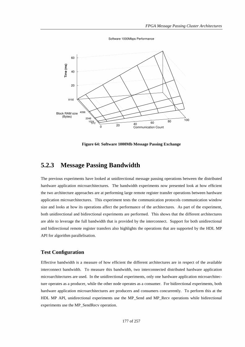
FPGA Message Passing Cluster Architectures
177 of 257
Figure 64: Software 1000Mb Message Passing Exchange
5.2.3 Message Passing Bandwidth
The previous experiments have looked at unidirectional message passing operations between the distributed
hardware application microarchitectures. The bandwidth experiments now presented look at how efficient
the two architecture approaches are at performing large remote register transfer operations between hardware
application microarchitectures. This experiment tests the communication protocols communication window
size and looks at how its operations affect the performance of the architectures. As part of the experiment,
both unidirectional and bidirectional experiments are performed. This shows that the different architectures
are able to leverage the full bandwidth that is provided by the interconnect. Support for both unidirectional
and bidirectional remote register transfers also highlights the operations that are supported by the HDL MP
API for algorithm parallelisation.
Test Configuration
Effective bandwidth is a measure of how efficient the different architectures are in respect of the available
interconnect bandwidth. To measure this bandwidth, two interconnected distributed hardware application
microarchitectures are used. In the unidirectional experiments, only one hardware application microarchitec-
ture operates as a producer, while the other node operates as a consumer. For bidirectional experiments, both
hardware application microarchitectures are producers and consumers concurrently. To perform this at the
HDL MP API, unidirectional experiments use the MP_Send and MP_Recv operations while bidirectional
experiments use the MP_SendRecv operation.
512 1024
2048
4096
8192
0 20 40 60 80 100
20
40
60
Tim
e (
ms)
Software 1000Mbps Performance
Block RAM size(Bytes)
Communication Count
Tim
e (
ms)

Evaluation
178 of 257
To measure the interconnect bandwidth, a large amount of data must be exchanged between the
hardware application microarchitectures. For the experiments, the target is to exchange 100,000,000 (108)
bytes between the hardware application microarchitectures in both unidirectional and bidirectional modes.
To calculate the interconnect bandwidth, the upper limit size of the communication is broken down into dif-
ferent sized message remote register transfers. Each hardware application microarchitecture exchanges data
using a known message size. The time to exchange the overall data reflects the performance of that message
size and the bandwidth that can be expected on the interconnect if that size of communication is used. Using
this information, it is possible to see how the network will affect data decomposition and distribution opera-
tions of an algorithm.
To exchange 100,000,000 bytes of data correctly, that amount of memory should ideally be avail-
able. For some of the 10/100 Mb Ethernet experiments, external DDR memory is used as the memory store.
For the remaining experiments, the use of on-FPGA Block RAMs, with appropriate wrap around logic, are
used to mimic the larger data sizes. This is not ideal however, the amount of Block RAM memory that is
available on newer FPGAs is constantly increasing. The hardware architecture is configured to read data
directly from the on-FPGA memory while the FPGA processor architecture reads data directly from applica-
tion memories, both configured as Block RAMs.
The DDR memory experiments test the design requirement that all memory on the FPGA is accessi-
ble to the network for performing remote register transfer operations, with only a subset of the experiments
using DDR memory. This reflects issues with the DDR controller for the 1000 Mb network relating to the
available memory bandwidth and modifications to the physical structure of the memory controller. The
FPGA compute units use individual DDR chips for the 1000 Mb network while the memory interface for the
100 Mb network system uses commodity DIMM memory. The DDR experiment results are useful when
looking at the performance of the parallel matrix multiplication as it uses DDR memory to store the matrix
data. DDR memory experiments were only possible with the hardware architecture. This arises as when
implementing the FPGA processor architecture for interfacing with the memory, issues with the memory
controller were identified which could not be easily fixed. The DDR memory experiment architecture evalu-
ates the direct access of the network logic to external DDR memory, a configuration suggested by both Un-
derwood [Underwood '01b] and Fuentes [Fuentes '06] but not directly evaluated by either.
All experiment parameters are uploaded to the FPGA cluster from the management node. Individ-
ual timers on each FPGA record the experiment elapsed clock cycles. These results are collated on the man-
agement node. The time to communicate with the head node is not recorded. Once the data is distributed, a
control signal starts the given experiment. The physical node architectures consist of all nodes performing
synchronisation and acknowledgement as per the message passing and communication algorithm presented
previously.

FPGA Message Passing Cluster Architectures
179 of 257
Slices Flip-Flops LUTs BRAM Frequency
(MHz)
Code Size
(Bytes)
Hardware,
Block RAM 5,001 3,948 8,269 76 103.618 N/A
FPGA processor,
Block RAM 5,533 5,633 8,705 87 107.984 12,396
DDR 5,718 4,686 9,388 20 105.313 N/A
DDR, Coherent 5,933 4,941 9,625 20 104.573 N/A
Table 21: Bandwidth Experiment Resource Utilisation
Experiment Outcome and Results
The main set of experiment results are presented by Figure 65 to Figure 68. Results are graphed based on the
switch that is used. This allows for a direct comparison of the two configurations, as both sets of results are
reflected on the graph. DDR memory experiment results are shown in Figure 69 and Figure 70.
The results show that based on efficiency across all interconnects the hardware architecture achieves
the best performance. The hardware architecture achieves between 90% and 95% as peak performance inde-
pendently of whether using unidirectional or bidirectional communications. The FPGA processor architec-
ture achieves a peak performance of 95% when running across unidirectional 100 Mb Ethernet. The ability
of the FPGA processor solution to achieve comparable performance with that of the hardware architecture
shows that the FPGA processor solution is efficiently implemented along with highlighting that the hardware
approach is able to saturate the interconnect. As the communication requirements change however, the
FPGA processor architecture is unable to achieve highly efficient bandwidth figures.
This can be seen as the performance of the bidirectional communications on both the 100 Mb
Ethernet and 1000 Mb Ethernet are basically the same. This shows that if a large amount of bidirectional
communication is required in the application, there may be little benefit in using a high speed interconnect
with its associated costs against the low speed interconnect solution presented by 100 Mb Ethernet. The ad-
ditional capacity provided by the higher speed network however may be of use if the system architecture is to
be changed at a later date, while a reduced latency would also be present.

Evaluation
180 of 257
Figure 65: FS108 Bandwidth
Figure 66: FS508 Bandwidth
20
40
60
80
100
120
140
160
180
200
103
104
105
106
107
108
Ba
nd
wid
th (
Mb
ps)
Message Size, Bytes
100Mb Network Bandwidth, FS108
Software, BidirectionalHardware, Bidirectional
Software, UnidirectionalHardware, Unidirectional
20
40
60
80
100
120
140
160
180
200
103
104
105
106
107
108
Ba
nd
wid
th (
Mb
ps)
Message Size, Bytes
100Mb Network Bandwidth, FS508
Software, BidirectionalHardware, Bidirectional
Software, UnidirectionalHardware, Unidirectional

FPGA Message Passing Cluster Architectures
181 of 257
Figure 67: Cisco Bandwidth
Figure 68: GS608 Bandwidth
20
40
60
80
100
120
140
160
180
200
103
104
105
106
107
108
Ba
nd
wid
th (
Mb
ps)
Message Size, Bytes
100Mb Network Bandwidth, Cisco
Software, BidirectionalHardware, Bidirectional
Software, UnidirectionalHardware, Unidirectional
200
400
600
800
1000
1200
1400
1600
1800
2000
103
104
105
106
107
108
Ba
nd
wid
th (
Mb
ps)
Message Size, Bytes
Gigabit Network Bandwidth, GS608
Software, BidirectionalHardware, Bidirectional
Software, UnidirectionalHardware, Unidirectional
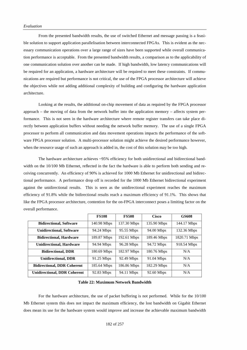
Evaluation
182 of 257
From the presented bandwidth results, the use of switched Ethernet and message passing is a feasi-
ble solution to support application parallelisation between interconnected FPGAs. This is evident as the nec-
essary communication operations over a large range of sizes have been supported while overall communica-
tion performance is acceptable. From the presented bandwidth results, a comparison as to the applicability of
one communication solution over another can be made. If high bandwidth, low latency communications will
be required for an application, a hardware architecture will be required to meet these constraints. If commu-
nications are required but performance is not critical, the use of the FPGA processor architecture will achieve
the objectives while not adding additional complexity of building and configuring the hardware application
architecture.
Looking at the results, the additional on-chip movement of data as required by the FPGA processor
approach – the moving of data from the network buffer into the application memory – affects system per-
formance. This is not seen in the hardware architecture where remote register transfers can take place di-
rectly between application buffers without needing the network buffer memory. The use of a single FPGA
processor to perform all communication and data movement operations impacts the performance of the soft-
ware FPGA processor solution. A multi-processor solution might achieve the desired performance however,
when the resource usage of such an approach is added in, the cost of this solution may be too high.
The hardware architecture achieves ~95% efficiency for both unidirectional and bidirectional band-
width on the 10/100 Mb Ethernet, reflected in the fact the hardware is able to perform both sending and re-
ceiving concurrently. An efficiency of 90% is achieved for 1000 Mb Ethernet for unidirectional and bidirec-
tional performance. A performance drop off is recorded for the 1000 Mb Ethernet bidirectional experiment
against the unidirectional results. This is seen as the unidirectional experiment reaches the maximum
efficiency of 91.8% while the bidirectional results reach a maximum efficiency of 91.1%. This shows that
like the FPGA processor architecture, contention for the on-FPGA interconnect poses a limiting factor on the
overall performance.
FS108 FS508 Cisco GS608
Bidirectional, Software 140.98 Mbps 137.30 Mbps 135.90 Mbps 144.17 Mbps
Unidirectional, Software 94.24 Mbps 95.55 Mbps 94.00 Mbps 132.36 Mbps
Bidirectional, Hardware 189.87 Mbps 192.61 Mbps 189.46 Mbps 1820.71 Mbps
Unidirectional, Hardware 94.94 Mbps 96.28 Mbps 94.72 Mbps 918.54 Mbps
Bidirectional, DDR 180.69 Mbps 182.97 Mbps 180.76 Mbps N/A
Unidirectional, DDR 91.25 Mbps 92.49 Mbps 91.04 Mbps N/A
Bidirectional, DDR Coherent 185.64 Mbps 186.86 Mbps 182.29 Mbps N/A
Unidirectional, DDR Coherent 92.83 Mbps 94.11 Mbps 92.60 Mbps N/A
Table 22: Maximum Network Bandwidth
For the hardware architecture, the use of packet buffering is not performed. While for the 10/100
Mb Ethernet system this does not impact the maximum efficiency, the lost bandwidth on Gigabit Ethernet
does mean its use for the hardware system would improve and increase the achievable maximum bandwidth
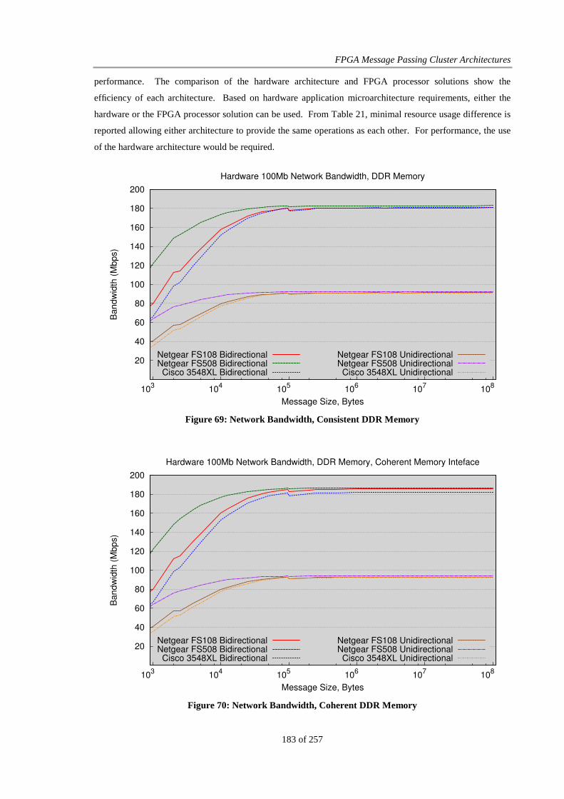
FPGA Message Passing Cluster Architectures
183 of 257
performance. The comparison of the hardware architecture and FPGA processor solutions show the
efficiency of each architecture. Based on hardware application microarchitecture requirements, either the
hardware or the FPGA processor solution can be used. From Table 21, minimal resource usage difference is
reported allowing either architecture to provide the same operations as each other. For performance, the use
of the hardware architecture would be required.
Figure 69: Network Bandwidth, Consistent DDR Memory
Figure 70: Network Bandwidth, Coherent DDR Memory
20
40
60
80
100
120
140
160
180
200
103
104
105
106
107
108
Bandw
idth
(M
bp
s)
Message Size, Bytes
Hardware 100Mb Network Bandwidth, DDR Memory, Coherent Memory Inteface
Netgear FS108 BidirectionalNetgear FS508 BidirectionalCisco 3548XL Bidirectional
Netgear FS108 UnidirectionalNetgear FS508 UnidirectionalCisco 3548XL Unidirectional
20
40
60
80
100
120
140
160
180
200
103
104
105
106
107
108
Ban
dw
idth
(M
bp
s)
Message Size, Bytes
Hardware 100Mb Network Bandwidth, DDR Memory
Netgear FS108 BidirectionalNetgear FS508 BidirectionalCisco 3548XL Bidirectional
Netgear FS108 UnidirectionalNetgear FS508 UnidirectionalCisco 3548XL Unidirectional

Evaluation
184 of 257
DDR Memory Bandwidth Measurements
Experiments looking at how the DDR memory interface impacts on the efficiency of the system have also
been performed, with the results shown in Figure 69 and Figure 70. As the DDR memory that is connected
to each node exceeds the 100,000,000 (108) byte limit that is used, all accesses for these bandwidth experi-
ments are to unique memory addresses. The tabulated peak bandwidth results for the experiments, Table 22,
show that only a marginal difference exists between the Block RAM and the DDR memory interfaces. Of
the interfaces however, the coherent configuration where data is only written back to memory if it has been
changed performs marginally better and is the interface that should be used if external memory is connected
directly to the on-FPGA SoC. A peak bandwidth of 189.87 Mbps is reported which is 94.9% efficient on the
link that is being used. This is measured when exchanging data from the Block RAM structures on the
FPGA. When the DDR memory interface is used, a peak bandwidth of 185.64 Mbps is reported, 92.8%
efficiency. This test validates the Send_Receive primitive of the HDL MP API and also validates the on-
FPGA memory interface logic that is used, as both Block RAM and system main memory have been inter-
faced with, for the exchange of data between the nodes. Access overheads that arise from using DDR mem-
ory, reduce the available system bandwidth however, the ability to access the data directly ensures an
efficient configuration is used. This is opposed to the overheads that would be introduced if the data is read
into application memory and transferred from there.
5.2.4 Benchmark Result Discussion
The benchmarks have measured the performance of the message passing and communication structures under
typical structural performance tests. From the results, the following information is of benefit and can be gen-
eralised into decisions that will arise when looking at an implementation based on switched Ethernet. Un-
managed switches provide the best performance in terms of lower latency and higher bandwidth however the
time difference would not warrant the overheads that will arise if dropped packets occur. The benchmark
tests are artificial as they do not generate or place a large strain on the switch interconnect so the effect a
dropped packets could have in these experiments can not be readily measured. For implementing a switched
Ethernet FPGA cluster, a managed switch is recommended as it will provide a more stable interconnect be-
tween devices and reduce the communication operations and network data communications that will be per-
formed. From the logic resource usage figures that are reported, the overheads of the soft processor approach
places a higher burden on the limited FPGA resources through using more Block RAM logic. The higher
logic usage of the soft processor in conjunction with the higher latency and lower bandwidth results make the
hardware implementation approach an ideal choice for performing all remote register transfer operations that
are required.
The Block RAM Exchange experiment provides a direct comparison of the expected data exchange
overheads that will arise for an application which is exchanging data between distributed Block RAMs.
From these results, the amount of parallelism that can be leverage can be investigated based on the expected
time to exchange the applications data. The results of this experiment aid the decision on whether a hardware
FPGA Message Passing Cluster Architectures
185 of 257
or a software approach to performing the remote register transfer operations is warranted. From the results, if
the time to exchange the data is not critical and the amount of parallelism present in the algorithm will not
overburden the FPGA resource usage, the soft processor approach would be ideal while if an algorithm re-
quires low latency or high bandwidth, the hardware approach along with 1000 Mb Ethernet will be required
to provide the best operational platform for the distributed application microarchitectures.
The bandwidth experiments show the maximum achievable performance for each architecture at all
times. From the results, if possible, bi-directional communications should always be performed as the most
efficient use of the available interconnect bandwidth while for a software platform, the use of a higher speed
interconnect is optional unless low latency is required. While the use of DDR memory was not possible as
part of the soft processor evaluation, the measured bandwidths offer an upper limit to the performance that
can be expected, as the soft processor approach does not support DMA operations between the memory ele-
ments and the network structures. This is opposed to the hardware approach where if DDR memory is re-
quired, the supported DMA operations allow an application to achieve nearly identical performance between
using internal Block RAM memory elements or external DDR memory for data storage. As is demonstrated
in the matrix multiplication experiment, when under application load, only a small drop-off in performance is
measured between the bandwidth experiments and that achieved as part of the experiment, which is discussed
further in Section 5.4.3.
5.3 Collective and Scalability Experiments
To measure scalability of using switched Ethernet and the structures of a parametric message passing inter-
face, HDL MP API, a range of collective experiments have been undertaken. These experiments look to
measure the ability of the HDL MP API to support a range of communication types on an algorithm by algo-
rithm basis, demonstrating scalability, and the ability of the distributed hardware application microarchitec-
tures to support fork-join parallelisation operations.
5.3.1 Message Passing Initialisation
The HDL MP API supports the initialisation of the message passing node identity to support scalable and
dynamic communications. To support this, all addressing structures are uploaded during FPGA cluster ini-
tialisation as against related systems where static addressing and routing is employed. To ensure correct op-
eration of the initialisation routines, each compute unit must be able to acquire a unique MAC address
specific to that compute unit. Two approaches have been used in this work. The first, using an on-board 1-
Wire ROM [Huang '01] that is present on the development board and the second, using input dip switches in
conjunction with an amount of preset address bits. The latter approach is used with Xilinx ML402 develop-
ment boards [Xilinx '06a], which do not contain the 1-Wire ROM chip.
The use of dynamic addresses allows each FPGA compute unit to have a unique MAC address and
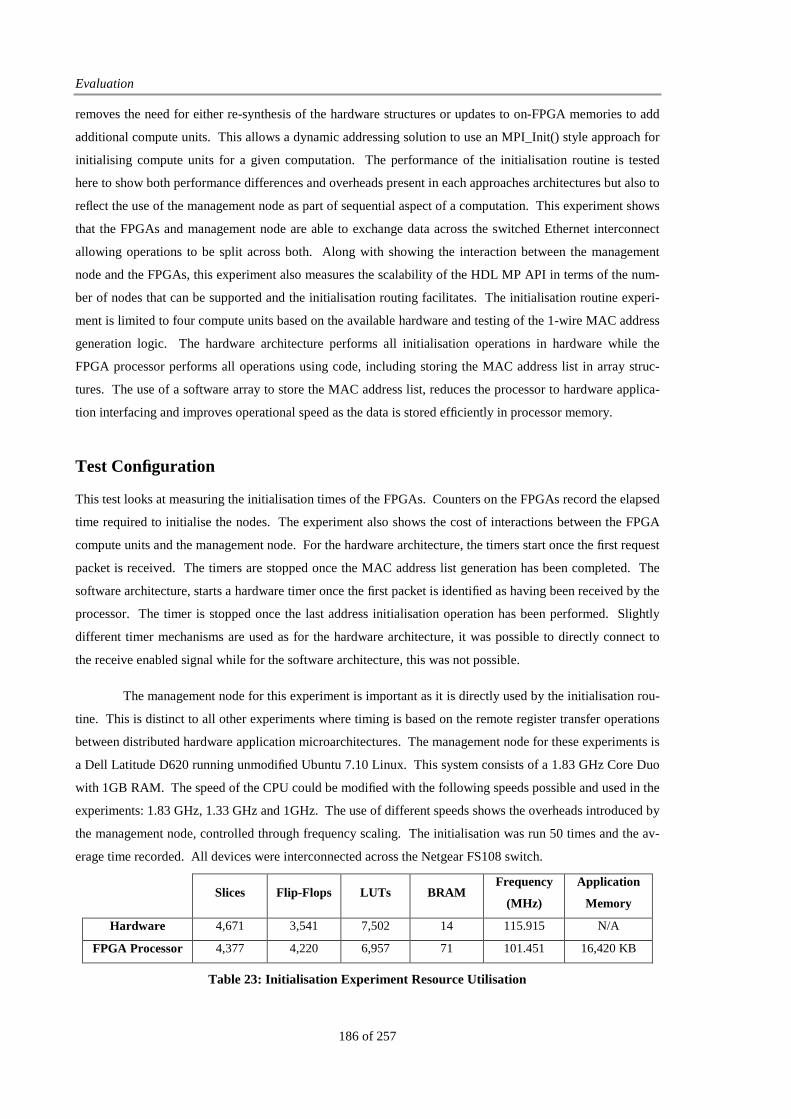
Evaluation
186 of 257
removes the need for either re-synthesis of the hardware structures or updates to on-FPGA memories to add
additional compute units. This allows a dynamic addressing solution to use an MPI_Init() style approach for
initialising compute units for a given computation. The performance of the initialisation routine is tested
here to show both performance differences and overheads present in each approaches architectures but also to
reflect the use of the management node as part of sequential aspect of a computation. This experiment shows
that the FPGAs and management node are able to exchange data across the switched Ethernet interconnect
allowing operations to be split across both. Along with showing the interaction between the management
node and the FPGAs, this experiment also measures the scalability of the HDL MP API in terms of the num-
ber of nodes that can be supported and the initialisation routing facilitates. The initialisation routine experi-
ment is limited to four compute units based on the available hardware and testing of the 1-wire MAC address
generation logic. The hardware architecture performs all initialisation operations in hardware while the
FPGA processor performs all operations using code, including storing the MAC address list in array struc-
tures. The use of a software array to store the MAC address list, reduces the processor to hardware applica-
tion interfacing and improves operational speed as the data is stored efficiently in processor memory.
Test Configuration
This test looks at measuring the initialisation times of the FPGAs. Counters on the FPGAs record the elapsed
time required to initialise the nodes. The experiment also shows the cost of interactions between the FPGA
compute units and the management node. For the hardware architecture, the timers start once the first request
packet is received. The timers are stopped once the MAC address list generation has been completed. The
software architecture, starts a hardware timer once the first packet is identified as having been received by the
processor. The timer is stopped once the last address initialisation operation has been performed. Slightly
different timer mechanisms are used as for the hardware architecture, it was possible to directly connect to
the receive enabled signal while for the software architecture, this was not possible.
The management node for this experiment is important as it is directly used by the initialisation rou-
tine. This is distinct to all other experiments where timing is based on the remote register transfer operations
between distributed hardware application microarchitectures. The management node for these experiments is
a Dell Latitude D620 running unmodified Ubuntu 7.10 Linux. This system consists of a 1.83 GHz Core Duo
with 1GB RAM. The speed of the CPU could be modified with the following speeds possible and used in the
experiments: 1.83 GHz, 1.33 GHz and 1GHz. The use of different speeds shows the overheads introduced by
the management node, controlled through frequency scaling. The initialisation was run 50 times and the av-
erage time recorded. All devices were interconnected across the Netgear FS108 switch.
Slices Flip-Flops LUTs BRAM Frequency
(MHz)
Application
Memory
Hardware 4,671 3,541 7,502 14 115.915 N/A
FPGA Processor 4,377 4,220 6,957 71 101.451 16,420 KB
Table 23: Initialisation Experiment Resource Utilisation
FPGA Message Passing Cluster Architectures
187 of 257
Experiment Outcome and Results
The initialisation time is presented in Figure 71. The cause for the drop in time related to one and two node
configurations for the hardware architecture has not been ascertained though close examination of the raw
data indicates that management node software overheads cause this. From Figure 71, the operating fre-
quency of the management node influences the initialisation time, as would be expected. For these experi-
ments, the operating frequency of the hardware architecture was 80MHz while the FPGA processor was
90MHz. The results of Figure 71 are the converted elapsed clock counts of each platform, taking in the op-
erational frequencies. Hardware initialisation times vary between 114 µs and 239 µs for the various man-
agement node processor speeds and cluster sizes. FPGA processor initialisation times vary between 157 µs
and 233 µs for the various management node processor speeds and cluster sizes. For comparison, an equiva-
lent test across the TCHPC Moloch cluster using gettimeofday() before and after the MPI_Init() call, reported
2.7 ms for one node to 108 ms for four nodes. Full flow control is employed at all times by the TCHPC Mo-
loch cluster while initialisation optimisations are present within the FPGA cluster, based on the closed net-
work configuration that is used
Synthesis results, Table 23, show the logic resource usage for the hardware and the FPGA processor
architectures used for this experiment. The results shown are for the architecture before the Ethernet control-
ler was updated for 1000 Mb operations. The synthesis results reflect preliminary operating performance for
the FPGA processor architecture. Further modifications to the FPGA processor system were based on the
120
140
160
180
200
220
240
1 Node 2 Nodes 3 Nodes 4 Nodes
Tim
e (
µs)
Node Count
FPGA Cluster Initialisation Timing
1830 MHz HW1830 MHz SW
1330 MHz HW1330 MHz SW
1000 MHz HW1000 MHz SW
Figure 71: Initialisation Timings
Evaluation
188 of 257
message passing communication interface, and not the operation of the initialisation routines, meaning the
times presented for the FPGA processor initialisation will not have changed based on these updates.
The initialisation routine experiment demonstrates the scalability that is possible from the HDL MP
API as a wide range of compute units have been supported easily. Further, the use of the abstract compute
unit identity allows for easy testing as no knowledge is required of the compute units themselves, rather that
they are connected to the interconnect and accessible from the management node. Taking the initialisation
routine experiments in connection with the benchmark experiments show the operations of the HDL MP API
are able to support a wide range of functionality. The next set of experiments look at the programmability of
the HDL MP API and how new communications can be added without modifying the application interface.
5.3.2 Barrier Synchronisation
As part of the HDL MP API programmability and scaling testing, Barrier Synchronisation experiments have
been performed between multiple distributed hardware application microarchitectures. This operation would
be used in a fork-join algorithm either before data is distributed to the compute units to ensure they are ready
to receive application data, or at the end of the parallel computations to ensure merging the results back to the
single control unit are performed correctly. The experiment uses the barrier synchronisation operations that
have been discussed in section 4.1.1. The implementation of the Barrier operations are based on rendezvous
mode, flow controlled packets. Barrier operations are built on top of the concurrent send and receive remote
register transfer operations for point-to-point communications.
Test Configuration
The barrier synchronisation test measures the time taken for the message passing and communication archi-
tectures to perform the synchronisation. The HDL MP API has been programmed to include the barrier syn-
chronisation state machines. Counters within the hardware application microarchitecture record the elapsed
time between first and last barrier call. To remove start up overhead delays, 1,000 barrier calls have been
measured with the average time taken as the measured barrier synchronisation overhead. As with previous
experiments, the hardware application microarchitecture used with both the hardware and FPGA processor
architectures is the same. To help evaluate the barrier experiment performances, an equivalent experiment
has been run on the TCHPC Moloch cluster. For the Moloch cluster experiment, an initial barrier is called to
synchronise all microprocessor compute units before the timer is started. Once all compute units have per-
formed this synchronisation operation, the timer is set and the required barrier counts are measured and re-
corded.

FPGA Message Passing Cluster Architectures
189 of 257
Experiment Outcome and Results
The results from the experiment are presented in Figure 72, with the synthesis results presented in Table 24,
as part of the overall collective communications results. The results demonstrate that the HDL MP API is
able to provide collective communication functionality while the underlying implementations are able to
support the collective communication algorithms. From latency experiments, the performance difference
between the hardware and software solutions is not that pronounced on a 100 Mb Ethernet network, until the
number of iterations that need to be performed increases – change between 3 and 4 nodes corresponds to an
increase from 1 to 2 communication iterations. The results show a result levelling off of the timing over-
heads when the number of nodes are within the same power of two bracket. This is expected from the algo-
rithm that is used where additional synchronisation remote register transfers are only required once the num-
ber of nodes increases its count into a new power of two value. This is seen in the experimental results where
the time to synchronise across two and three nodes are nearly identical while the time to synchronise across
four and five nodes are nearly identical.
The TCHPC Moloch cluster experiments show the performance and operations of a barrier commu-
nication on a commodity cluster. While the performance figures are similar to the FPGA configurations, it
should be remembered that the Moloch cluster operates across a gigabit Ethernet network. The results form
this cluster show improvements when the number of nodes is a power of two. Further investigations, not
reported in Figure 72, reveal that optimisations are present when the number of cluster nodes is a power of
two. These further investigations are based on extending the cluster test to higher compute units counts. A
reduction in the barrier latency was measured between 7 and 8 compute units while increases were measured
50
100
150
200
250
2 3 4 5
Tim
e (
µs)
Node Count
Barrier Synchronisation Comparison
Netgear FS108 HW - FPGANetgear FS508 HW - FPGA
Cisco 3548XL HW- FPGACisco 4006 - Moloch
Netgear FS108 SW - FPGANetgear FS508 SW - FPGA
Cisco 3548XL SW- FPGA
Figure 72: Barrier Synchronisation Times

Evaluation
190 of 257
between 6 and 7. This would lead to the belief that specific optimisations have been applied when the num-
ber of compute units is a power of two. The microprocessor MPI uses MPICH version 1.2.5.2 using
MPIexec Version 0.76, configuration options:'--with-default-comm=mpich-p4' '--with-pbs=/usr/support/pbs'
'--prefix=/usr/support' '--disable-p4-shmem'
5.3.3 Collective Communications
Further to the collective communications of the initialisation and barrier synchronisation, additional collec-
tive communications, discussed in Section 4.1.1, have been implemented and tested in simulation. These
simulations show that like the barrier, use of the different collective communications can be programmed into
the HDL MP API, extending the communication styles that are available to the hardware application mi-
croarchitecture for remote register transfer. As the HDL MP API has been shown to operate correctly for
both the hardware microarchitecture and the software FPGA processor, the collective communication simula-
tions are only performed with the hardware microarchitecture. The hardware microarchitecture simulation
environment provides a more realistic simulation as multiple distributed hardware application microarchitec-
tures can be interconnected across a simulation Ethernet switch. Performance figures, Table 24 and Table 25,
are based on using Block RAM memories and show the resource usage overhead associated with each collec-
tive communication as part of the HDL MP API.
Slices Flip-Flops LUTs BRAM Frequency
(MHz)
Base, Blocking 4,394 4,113 7,055 12 126.815
Base, Non-Blocking 5,996 4,271 8,348 12 126.815
Barrier 4,501 4,188 7,252 12 126.815
Broadcast 5,148 4,764 8,198 12 126.815
Scatter 4,679 4,259 7,227 12 126.815
Gather 4,404 4,255 7,227 12 126.815
AllGather 4,308 4,532 7,404 12 117.472
AllToAll 4,575 4,543 7,433 12 117.472
Table 24: Hardware Collective Operations Logic Footprint. Resource usage is based on blocking
flow controlled communications employing split fragmentation
The results in Table 24 and Table 25 show the resource usage differences between various HDL MP
API capable interfaces. The base resource usage figures show the point-to-point remote register transfer ar-
chitecture requirements to support data exchange and synchronisation between the distributed hardware ap-
plication microarchitectures. For the hardware results, the non-blocking interface results are also reported.
The non-blocking interface, detailed in Section 4.2.1, show the resource usage overheads required in this
implementation for supporting multiple concurrent remote register transfer operations. The collective com-
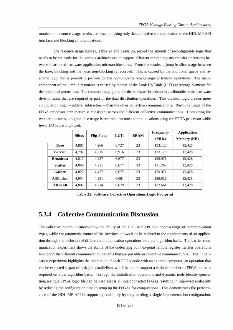
FPGA Message Passing Cluster Architectures
191 of 257
munication resource usage results are based on using only that collective communication in the HDL MP API
interface and blocking communications.
The resource usage figures, Table 24 and Table 25, record the amount of reconfigurable logic that
needs to be set aside for the various architectures to support different remote register transfer operations be-
tween distributed hardware application microarchitectures. From the results, a jump in slice usage between
the base, blocking and the base, non-blocking is recorded. This is caused by the additional queue and re-
source logic that is present to provide for the non-blocking remote register transfer operations. The major
component of the jump in resources is caused by the use of the Look Up Table (LUT) as storage elements for
the additional queue data. The resource usage jump for the hardware broadcast is attributable to the hardware
division units that are required as part of the data distribution operations. This division logic creates more
computation logic – adders, subtractors – than the other collective communications. Resource usage of the
FPGA processor architecture is consistent across the different collective communications. Comparing the
two architectures, a higher slice usage is recorded for most communications using the FPGA processor while
fewer LUTs are employed.
Slices Flip-Flops LUTs BRAM Frequency
(MHz)
Application
Memory (KB)
Base 4,885 4,266 6,727 23 133.120 12,428
Barrier 4,797 4,315 6,916 23 133.120 12,428
Broadcast 4,817 4,237 6,677 23 129.971 12,428
Scatter 4,866 4,231 6,677 23 131.268 12,428
Gather 4,827 4,427 6,677 23 129.971 12,428
AllGather 4,954 4,231 6,681 23 129.921 12,428
AllToAll 4,807 4,214 6,679 23 132.661 12,428
Table 25: Software Collective Operations Logic Footprint
5.3.4 Collective Communication Discussion
The collective communications show the ability of the HDL MP API to support a range of communication
types, while the parametric nature of the interface allows it to be tailored to the requirements of an applica-
tion through the inclusion of different communication operations on a per algorithm basis. The barrier com-
munication experiment shows the ability of the underlying point-to-point remote register transfer operations
to support the different communication patterns that are possible in collective communications. The initiali-
sation experiment highlights the interaction of each FPGA node with an external computer, an operation that
can be expected as part of fork-join parallelism, which is able to support a variable number of FPGA nodes as
required on a per algorithm basis. Through the initialisation operations and dynamic node identity genera-
tion, a single FPGA logic file can be used across all interconnected FPGAs resulting in improved scalability
by reducing the configuration time to setup up the FPGAs for computations. This demonstrates the perform-
ance of the HDL MP API in supporting scalability by only needing a single implementation configuration.

Evaluation
192 of 257
Through the parametric operation of the HDL MP API, a range of collective communications can be included
as necessary, allowing for tailoring of the implementation to an algorithms requirements as opposed to im-
plementing all operations which may or may not always be required.
From the resource usage results that are presented, Table 24 and Table 25, the hardware only im-
plementation uses the least amount of resources when measured by slices which will result in more resources
being available for a distributed hardware application microarchitecture. The collective communications also
show that the layered implementation approach that has been taken can be easily extended to include differ-
ent communication patterns and operations as these have been layered on top of the functionality of the
point-to-point communications. As part of the collective communications, an objective was to interface
hardware collective communication state machines with the point-to-point mechanism independently of the
manner point-to-point communications are to be performed – hardware or software. This approach has not
previously been demonstrated, rather the use of software to support FPGA cluster collective communications
has been shown for the TMD-MPI while the use of hardware only collective communications has not been
demonstrated. The experiments and simulations of the collective communications shown here are novel from
that perspective while the use of single interconnect to support their operations is also an advance on other
comparable solutions – RCC, FHPCA – where additional networks and resources are needed.
The next section looks to use the hardware microarchitecture to support the remote register transfer
operations of a high performance application, parallel matrix multiplication. This tests both the structures of
the communication hardware microarchitecture and the operations of the HDL MP API in supporting parallel
computations of hardware application microarchitectures.
5.4 Parallel Matrix Multiplication
Experiments looking at the performance and capabilities of the HDL MP API in supporting remote register
transfer operations between distributed hardware application microarchitectures are based on using parallel
matrix multiplication. Parallel matrix multiplication using the details presented in previous chapters has been
implemented and a range of experiments, detailed here have been performed to measure the functionality and
performance of the HDL MP API. As mentioned above, these experiments are performed using the hardware
communication microarchitecture as it provides certain performance advantages which better support the
parallel matrix multiplication experiments. A number of experiments have been performed, each looking to
measure certain aspects of the HDL MP API and its operations. The first looks at using classical matrix mul-
tiplication to test the parallelisation of the algorithm across multiple FPGAs. This allows testing of the HDL
MP API interface, the memory interface and data parallelisation which is used in the algorithm. The second
set of experiments use the linear array architecture as the computation logic. A number of experiments have
been performed using the linear array, measuring different aspects of the architecture. The first set of ex-
periments form the basis of the publication [Creedon '08] and were undertaken before the HDL MP API was
updated to use burst data transfers. To see the effect that the burst accesses have on the performance of the
computations, the same experiments were performed again across the same experiment sizes with the results

FPGA Message Passing Cluster Architectures
193 of 257
presented below. Finally, to help put the results of the parallel matrix multiplication into perspective, results
from using a commodity cluster, Moloch and MPI are also presented.
5.4.1 Classical Parallel Configuration
The classical parallel matrix multiplication architecture is used to test the data decomposition and communi-
cation ring topology that will be used for the high performance linear array architecture. This shows that the
platform is able to support computations and communications of a parallel application, using the HDL MP
API. The classical implementation has been developed to provide preliminary testing of the HDL MP API
under parallel computation and communication loads. The classical implementation does not perform or
look into any optimisations, including timing closure and has been developed purely to allow for testing of
the HDL MP API and the communication systems. The classical implementation looks at ensuring the cor-
rect operation of the data decomposition and communication patterns while also offering a verification plat-
form against which the linear array microarchitecture can be compared. The computation results of the clas-
sical implementation are verified against software running on the management node.
Test Configuration
For the classical parallel matrix multiplication multiple compute units are interconnected, with the number of
compute units specified and configured during system initialisation, with 1 to 4 nodes possible as part of the
FPGA cluster. The number of compute units is dictated by the amount of hardware that is available, and is
not based on any known hardware implementation restrictions. Following the results and experience of the
classical matrix multiplication, the HDL MP API was updated to a single command interface, to better sup-
port the remote register transfer operations of different distributed hardware microarchitectures. The HDL
MP API interfaces used in classical matrix multiplications is based on a two channel command interface,
with all control logic duplicated for each new remote register transfer interface that could be used. By using
the two channels, autonomous concurrent remote register transfers are supported but this interface does not
easily lend itself to supporting the expandability and programmability already discussed. For the experi-
ments, the computations are performed before the remote register transfer operations are performed. This
allows for testing of the HDL MP API in supporting both the computations and remote register transfer op-
erations without increasing the complexity of testing each.
Horizontal data decomposition with linear data distribution is used for the parallel system. Remote
register transfer data exchange is based on transferring the B matrix data between the distributed hardware
application microarchitectures using a ring communication topology. The result data, C matrix, is stored on
each FPGA based on the compute unit identity and the computation iteration that is used. This allows for
more efficient result readback as very little data post processing is required on the management node.
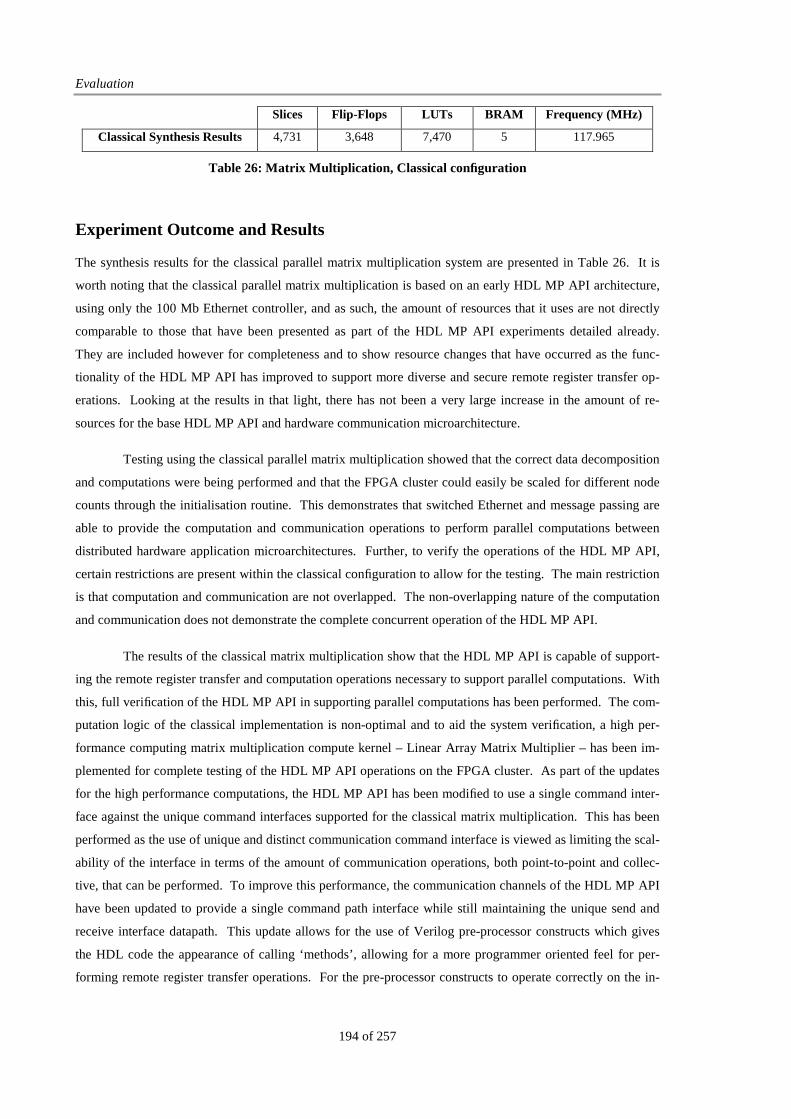
Evaluation
194 of 257
Slices Flip-Flops LUTs BRAM Frequency (MHz)
Classical Synthesis Results 4,731 3,648 7,470 5 117.965
Table 26: Matrix Multiplication, Classical configuration
Experiment Outcome and Results
The synthesis results for the classical parallel matrix multiplication system are presented in Table 26. It is
worth noting that the classical parallel matrix multiplication is based on an early HDL MP API architecture,
using only the 100 Mb Ethernet controller, and as such, the amount of resources that it uses are not directly
comparable to those that have been presented as part of the HDL MP API experiments detailed already.
They are included however for completeness and to show resource changes that have occurred as the func-
tionality of the HDL MP API has improved to support more diverse and secure remote register transfer op-
erations. Looking at the results in that light, there has not been a very large increase in the amount of re-
sources for the base HDL MP API and hardware communication microarchitecture.
Testing using the classical parallel matrix multiplication showed that the correct data decomposition
and computations were being performed and that the FPGA cluster could easily be scaled for different node
counts through the initialisation routine. This demonstrates that switched Ethernet and message passing are
able to provide the computation and communication operations to perform parallel computations between
distributed hardware application microarchitectures. Further, to verify the operations of the HDL MP API,
certain restrictions are present within the classical configuration to allow for the testing. The main restriction
is that computation and communication are not overlapped. The non-overlapping nature of the computation
and communication does not demonstrate the complete concurrent operation of the HDL MP API.
The results of the classical matrix multiplication show that the HDL MP API is capable of support-
ing the remote register transfer and computation operations necessary to support parallel computations. With
this, full verification of the HDL MP API in supporting parallel computations has been performed. The com-
putation logic of the classical implementation is non-optimal and to aid the system verification, a high per-
formance computing matrix multiplication compute kernel – Linear Array Matrix Multiplier – has been im-
plemented for complete testing of the HDL MP API operations on the FPGA cluster. As part of the updates
for the high performance computations, the HDL MP API has been modified to use a single command inter-
face against the unique command interfaces supported for the classical matrix multiplication. This has been
performed as the use of unique and distinct communication command interface is viewed as limiting the scal-
ability of the interface in terms of the amount of communication operations, both point-to-point and collec-
tive, that can be performed. To improve this performance, the communication channels of the HDL MP API
have been updated to provide a single command path interface while still maintaining the unique send and
receive interface datapath. This update allows for the use of Verilog pre-processor constructs which gives
the HDL code the appearance of calling ‘methods’, allowing for a more programmer oriented feel for per-
forming remote register transfer operations. For the pre-processor constructs to operate correctly on the in-
FPGA Message Passing Cluster Architectures
195 of 257
terface logic, all communication operations on the interface must be performed as part of a single always
construct, which is not possible if the interface signal is set in multiple locations.
5.4.2 Multi-Node Parallel Linear Array Matrix Multiplicat ion
The linear array and control logic microarchitecture, described previously, has been integrated with the re-
mote register transfer operations of the classical parallel matrix multiplication architecture. Parallel matrix
multiplication is an EP computation which requires a large amount of memory bandwidth against the amount
of remote register transfer operations. This operation coupled to the size of the remote register transfer,
which is larger than 100 MB for some experiments, provides the testing environment for the operations of the
HDL MP API in supporting parallel computations between distributed hardware application microarchitec-
tures, using switched Ethernet and message passing.
The communication operations of the parallel matrix multiplication call for an initial data set for
both matrix A and B, followed by a bidirectional remote register transfer between the hardware application
microarchitectures. This remote register transfer is performed concurrently to ongoing computations, allow-
ing for data pre-fetch operations which hide the communication network latencies. To reduce the complexity
of performing computations and communications on large data sets, the hardware communication microar-
chitecture is required to transfer data directly from external memory while the hardware application microar-
chitecture is responsible for accessing the application memory that it needs. The concurrent access of com-
pute unit memory is supported by the on-FPGA SoC interconnect.
As part of the implementation of the parallel linear array microarchitecture, tests were performed
both in simulation and across the FPGAs to verify all operations are performed correctly. As part of these
verification experiments, smaller matrix sizes running across fewer processing elements were used.
Linear Array Performance Testing
Before detailing the tests of the high performance parallel matrix multiplication, details on a standalone linear
array unit are presented. While testing the operation of the linear array, simulations using a single linear ar-
ray were used to test the movement of data between the interconnected processing elements and external
DDR memory. As part of this, simulations on the number of processing elements that could fit on an FPGA
if the hardware communications microarchitecture was not present were undertaken. This allows for easy
simulation testing of the linear array and the data exchange mechanisms used between processing elements.
Through the use of the HDL MP API memory interface, it was possible to connect the linear array directly to
the AMBA memory interface without requiring a change to the linear array. By interfacing directly with the
memory interface fewer resources are used. Implementation testing and synthesis results showed that a total
of 14 processing elements, running at 125MHz, could be catered for on a single FPGA, yielding a maximum
throughput of 3500 Megabyte Floating-Point Operations Per Second (MFLOPS) for the linear array. Per-
formance measurements of the single linear array architecture were not taken. However, the simulation re-
Evaluation
196 of 257
sults and computation operations were directly applicable to the parallel matrix multiplication experiments.
This was easily facilitated by the HDL MP API which meant that no changes were required on the hardware
application microarchitecture. Changes were only needed to interface the HDL MP API with the hardware
communication microarchitecture and its structures. Once the linear array was shown to exchange data cor-
rectly, full testing with the distributed hardware application microarchitectures and remote register transfer
operations were undertaken. These experiments are now detailed.
Test Configuration
Two distinct experiments have been performed on the parallel linear array matrix multiplication, testing two
aspects of the performance and operation of the HDL MP API, the hardware communication architecture and
the behaviour of the FPGA cluster, the results of which have been presented in Creedon and Manzke FPL
2008 [Creedon '08]. For the experiments, the FPGA cluster compute units have been interconnected across
the Cisco switch that is being used. All on-FPGA interconnect operations are based on non-burst, memory
aligned accesses.
Experiment One, The Scaling Test: This experiment looks at how the communication and computation
logic scale as the size of the computations and communication data are scaled based on the number of
distributed hardware application microarchitectures used. A base set of results are gathered, which show
the performance of a single linear array microarchitecture. As more nodes are added, the same matrix
sizes are scaled to reflect the higher compute unit count. This test measures the remote register transfer
operations overheads and how these affect the performance of the linear array. This is seen as if no im-
pact is recorded, a 100% improvement in computation performance should be recorded. Any drop below
this reflects overheads that the remote register transfer operations introduce. The upper limit for the scal-
ing test is when the memory footprint for performing the computations completely fills the FPGA cluster
nodes memory.
Experiment Two, The Parallel Test: The parallel performance of the platform is measured in this experi-
ment. This experiment looks at the speed-ups that are achieved by parallelising the computations over
multiple hardware application microarchitectures. Starting from a larger matrix whose result is com-
puted on a single FPGA – from the scaling test – the matrix data is appropriately divided across the ap-
plication microarchitectures to perform the parallel computations. As part of this experiment, the per-
formance across multiple nodes is measured in relation to the size of matrix that can be computed. This
sees the scaling and parallel test expanded so that the size of the computations can be increased for the
given amount of computation resources.
The linear array microarchitecture is designed to accept parameter uploading to control the size of
the matrices that are being used in the computation. Parameter uploading is performed within certain restric-
tions caused by the control logic implemented as part of the linear array, not by any problems with the HDL
MP API and remote register transfer operations. The parameterised test upload allows for different computa-
tion grid sizes, which highlight the trade-off between the A and B matrix buffer sizes. All computation pa-
rameters are transmitted to the FPGA compute units before the computation commences. To ensure the

FPGA Message Passing Cluster Architectures
197 of 257
hardware operates correctly at 100MHz, a dataflow structure is used to generate the matrix address and data
offsets inline as the computation parameters are received by the hardware application microarchitecture con-
trol logic. For the dataflow structure, the various matrix address pointers are generated based on the compu-
tation sizes e.g. B matrix address base pointers for the two buffers that are present, the C matrix base address
pointer given the B matrix sizes that are being used.
Slices Flip-Flops LUTs BRAM Frequency
(MHz)
HDL MP API
Structures
5,239 /
13,696
4,116 /
30,816
8,523 /
30,816 17 / 136 108.009
Single
Processing
Element
854 / 13,696 699 / 30,816 1,302 /
30,816 10 / 136 159.848
Linear
Array
9,148 /
13,696
9,136 /
30,816
15,695 /
30,816 100 / 136 118.918
FPGA Cluster
Node
12,501 /
13,696
12,979 /
30,816
22,939 /
30,816 117 / 136 98.6546
Table 27: Linear Array, Parallel Matrix Multiplicat ion Experiment Resource
Utilisation. Maximum available resources are shown after the /
Experiment Outcome and Results
All matrix multiplication results presented as part of the HDL MP API experiments are run at 100MHz, with
the linear array structure consisting of 10 single precision floating point processing elements. This yields a
maximum throughput of 2000 MFLOPS for each linear array. The synthesis results for the initial HDL MP
API architecture are presented in Table 27. The synthesis results are presented built on the operations of the
lower logic. For the results this means a direct increase in the resource utilisation will not occur as certain
functionality is merged by the synthesis tools as the logic operations of other layers are taken into considera-
tion. The synthesis results fill the FPGA nodes that are being used for the verification, and it is for this rea-
son that a 10 unit linear array configuration has been used for the verification experiments.
Scaling Test
The scaling test measures performance drop off that is recorded as the number of compute units of the FPGA
cluster is increased. This drop in performance is caused by the additional remote register transfer operation
overheads that are introduced as more memory accesses are present to move the data between the hardware
application microarchitectures. The scaling test presents a directly comparable architecture to measure the
overheads that are present when memory access is shared between the computation and the communication
6 As taken from the synthesis report. Place and route optimisations met the 100 MHz.
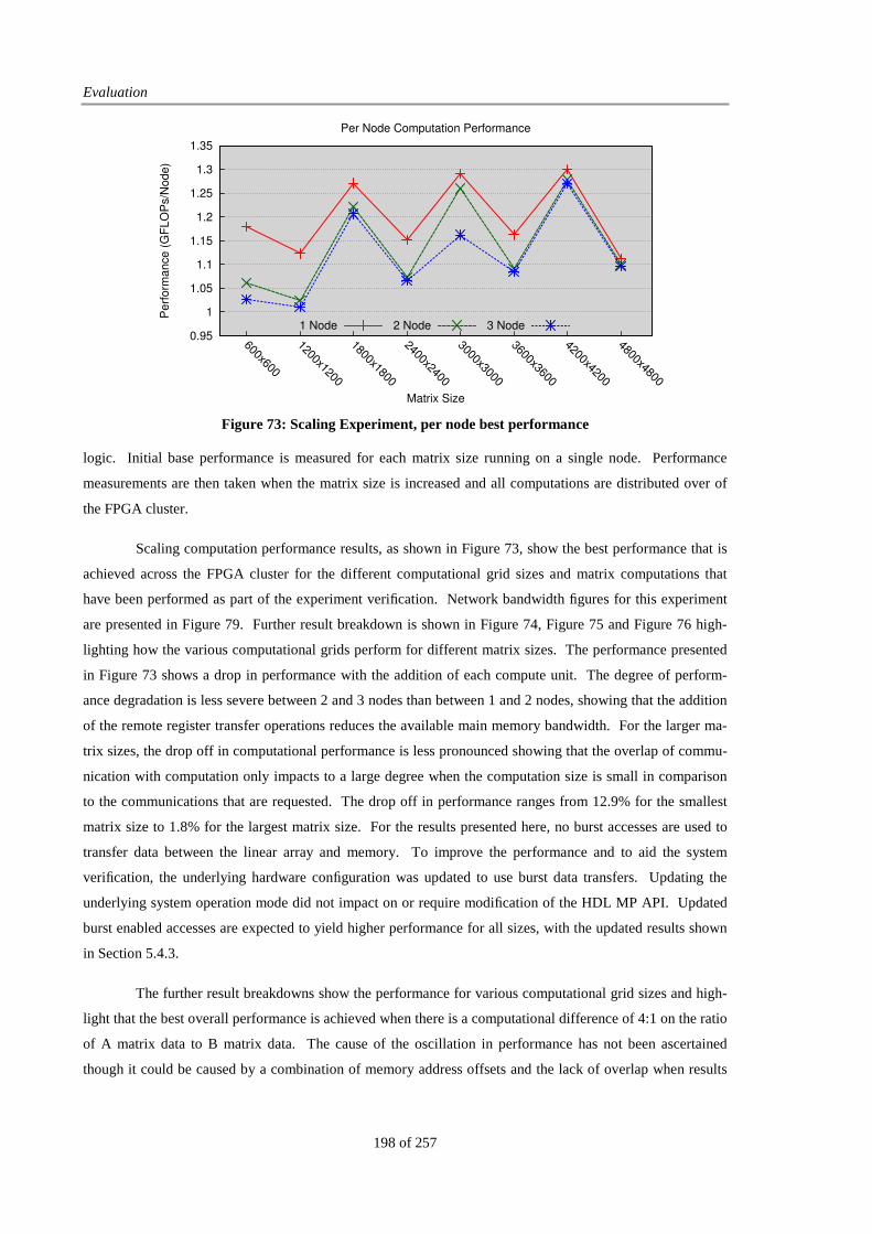
Evaluation
198 of 257
logic. Initial base performance is measured for each matrix size running on a single node. Performance
measurements are then taken when the matrix size is increased and all computations are distributed over of
the FPGA cluster.
Scaling computation performance results, as shown in Figure 73, show the best performance that is
achieved across the FPGA cluster for the different computational grid sizes and matrix computations that
have been performed as part of the experiment verification. Network bandwidth figures for this experiment
are presented in Figure 79. Further result breakdown is shown in Figure 74, Figure 75 and Figure 76 high-
lighting how the various computational grids perform for different matrix sizes. The performance presented
in Figure 73 shows a drop in performance with the addition of each compute unit. The degree of perform-
ance degradation is less severe between 2 and 3 nodes than between 1 and 2 nodes, showing that the addition
of the remote register transfer operations reduces the available main memory bandwidth. For the larger ma-
trix sizes, the drop off in computational performance is less pronounced showing that the overlap of commu-
nication with computation only impacts to a large degree when the computation size is small in comparison
to the communications that are requested. The drop off in performance ranges from 12.9% for the smallest
matrix size to 1.8% for the largest matrix size. For the results presented here, no burst accesses are used to
transfer data between the linear array and memory. To improve the performance and to aid the system
verification, the underlying hardware configuration was updated to use burst data transfers. Updating the
underlying system operation mode did not impact on or require modification of the HDL MP API. Updated
burst enabled accesses are expected to yield higher performance for all sizes, with the updated results shown
in Section 5.4.3.
The further result breakdowns show the performance for various computational grid sizes and high-
light that the best overall performance is achieved when there is a computational difference of 4:1 on the ratio
of A matrix data to B matrix data. The cause of the oscillation in performance has not been ascertained
though it could be caused by a combination of memory address offsets and the lack of overlap when results
0.95
1
1.05
1.1
1.15
1.2
1.25
1.3
1.35
600x600
1200x1200
1800x1800
2400x2400
3000x3000
3600x3600
4200x4200
4800x4800
Pe
rfo
rma
nce
(G
FL
OP
s/N
od
e)
Matrix Size
Per Node Computation Performance
1 Node 2 Node 3 Node
Figure 73: Scaling Experiment, per node best performance

FPGA Message Passing Cluster Architectures
199 of 257
are written back to memory. Depending on the system behaviour that is required, stable increase in computa-
tional performance is noted when a 10:1 ratio is used between the A matrix and B matrix data sizes.
The network bandwidth performance has also been measured for the 2 and 3 node configurations,
shown in Figure 79. Better network performance is measured for two nodes, when less interconnect conten-
tion is present. The scaling test verifies the interfacing between the hardware application microarchitecture,
the network and the memory system for performing remote register transfer operations while also showing
the amount of computation operations that can be performed. The scaling verification test show that it is pos-
sible for the HDL MP API to use the system memory for performing compute intensive applications. This is
seen as it was possible to directly increase the computation size and amount of computation data without ei-
ther modifying or otherwise changing the hardware application microarchitecture. Further, it was possible to
access and operate all the memory that was connected to an individual node directly from both the hardware
application microarchitecture and the network remote register transfer operations.
0.6
0.7
0.8
0.9
1
1.1
1.2
1.3
1.4
600x600
1200x1200
1800x1800
2400x2400
3000x3000
3600x3600
4200x4200
4800x4800
Pe
rfo
rma
nce
(G
FL
OP
s)
Matrix Size
Matrix Multiplication, 1 Node
200 x 20200 x 15
120 x 30100 x 30
60 x 6050 x 60
Figure 74: Matrix Multiplication Performance Breakd own, 1 Node

Evaluation
200 of 257
0.6
0.7
0.8
0.9
1
1.1
1.2
1.3
1.4
600x600
1200x1200
1800x1800
2400x2400
3000x3000
3600x3600
4200x4200
4800x4800
Pe
rfo
rma
nce
(G
FL
OP
s/n
od
e)
Matrix Size
Matrix Multiplication, 2 Node
200 x 20200 x 15
120 x 30100 x 30
60 x 6050 x 60
Figure 75: Matrix Multiplication Performance Breakd own, 2 Nodes
0.6
0.7
0.8
0.9
1
1.1
1.2
1.3
1.4
600x600
1200x1200
1800x1800
2400x2400
3000x3000
3600x3600
4200x4200
4800x4800
Perf
orm
ance (
GF
LO
Ps/n
ode)
Matrix Size
Matrix Multiplication, 3 Node
200 x 20200 x 15
120 x 30100 x 30
60 x 6050 x 60
Figure 76: Matrix Multiplication Performance Breakd own, 3 Nodes
Parallel Test
Parallel computation testing, where a known problem size is split across multiple hardware application mi-
croarchitectures to reduce the time to perform computations, has been performed as part of the hardware sys-
tem verification testing. The parallel test is used to measure computation speed ups when additional nodes
are added and configured to perform the computation concurrently to the other nodes. This test measures

FPGA Message Passing Cluster Architectures
201 of 257
system speed ups that are recorded and further verifies the HDL MP API interface as the performance meas-
urements look at more directly measuring the performance of the hardware only message passing environ-
ment. This test measures the speed-ups that are achieved for a given problem size when additional hardware
application microarchitectures are added. Connected with this experiment is a measure of the maximum size
that can be computed across the FPGA cluster with the computation time reported. Parallel performance
measurements are presented in Figure 77, with computational speed-ups for the various node counts are pre-
sented in Figure 78. Network bandwidth performance is shown in Figure 79.
One of the merits of supporting remote register transfer between distributed hardware application
microarchitectures is the ability to easily increase the size of the computation that is being performed once
the reconfigurable resources of a compute unit are exhausted. This is measured in the parallel computation
by the ever increasing size of the matrix. For these results, once the matrix size was too great to fit in avail-
able memory, testing on that number of hardware application microarchitecture compute units was stopped.
This can be seen between the 1 node and 2, 3 node experiments once a matrix size of 5400x5400 was to be
computed. Each FPGA compute unit has 512 MB of data that is segmented, 128 MB for the A matrix, 256
MB for the B matrix, split between the two B matrix buffers and 128 MB for the C matrix. A matrix size of
5400x5400 single precision, requires 111 MB of available storage per matrix. 6000x6000 requires 137 MB
of available storage which is outside the limits of a single node. The maximum size that can be computed
across the 3 nodes is a 9600x9600 matrix.
0
100
200
300
400
500
600x600
1200x1200
1800x1800
2400x2400
3000x3000
3600x3600
4200x4200
4800x4800
5400x5400
6000x6000
6600x6600
7200x7200
7800x7800
8400x8400
9000x9000
9600x9600
Com
puta
tion T
ime (
seconds)
Matrix Size
Parallel Computation Times
1 Node FPGA2 Node FPGA3 Node FPGA
Figure 77: Parallel Matrix Multiplication Times
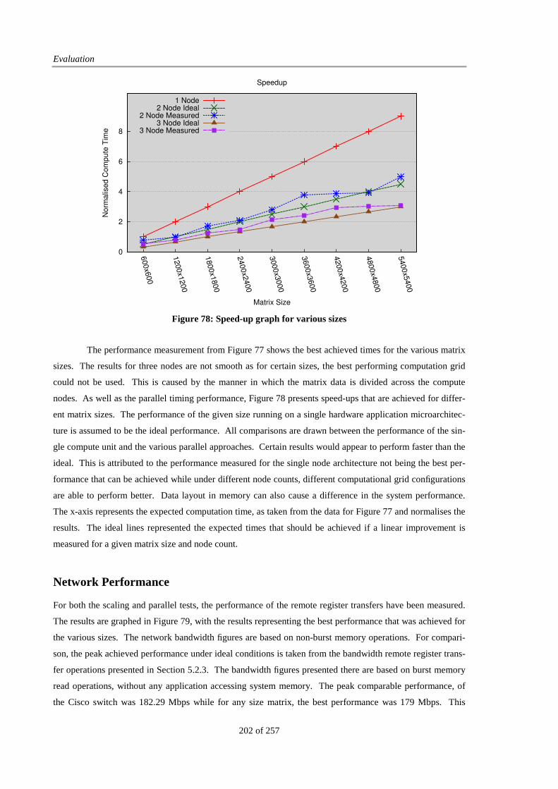
Evaluation
202 of 257
The performance measurement from Figure 77 shows the best achieved times for the various matrix
sizes. The results for three nodes are not smooth as for certain sizes, the best performing computation grid
could not be used. This is caused by the manner in which the matrix data is divided across the compute
nodes. As well as the parallel timing performance, Figure 78 presents speed-ups that are achieved for differ-
ent matrix sizes. The performance of the given size running on a single hardware application microarchitec-
ture is assumed to be the ideal performance. All comparisons are drawn between the performance of the sin-
gle compute unit and the various parallel approaches. Certain results would appear to perform faster than the
ideal. This is attributed to the performance measured for the single node architecture not being the best per-
formance that can be achieved while under different node counts, different computational grid configurations
are able to perform better. Data layout in memory can also cause a difference in the system performance.
The x-axis represents the expected computation time, as taken from the data for Figure 77 and normalises the
results. The ideal lines represented the expected times that should be achieved if a linear improvement is
measured for a given matrix size and node count.
Network Performance
For both the scaling and parallel tests, the performance of the remote register transfers have been measured.
The results are graphed in Figure 79, with the results representing the best performance that was achieved for
the various sizes. The network bandwidth figures are based on non-burst memory operations. For compari-
son, the peak achieved performance under ideal conditions is taken from the bandwidth remote register trans-
fer operations presented in Section 5.2.3. The bandwidth figures presented there are based on burst memory
read operations, without any application accessing system memory. The peak comparable performance, of
the Cisco switch was 182.29 Mbps while for any size matrix, the best performance was 179 Mbps. This
0
2
4
6
8
600x600
1200x1200
1800x1800
2400x2400
3000x3000
3600x3600
4200x4200
4800x4800
5400x5400
Norm
alis
ed C
om
pute
Tim
e
Matrix Size
Speedup
1 Node2 Node Ideal
2 Node Measured3 Node Ideal
3 Node Measured
Figure 78: Speed-up graph for various sizes

FPGA Message Passing Cluster Architectures
203 of 257
shows that on a pure peak performance measurement, there is a drop of some 3 Mbps when the application
logic is introduced. This peak performance is measured between two hardware application microarchitec-
tures and represents the peak performance that was measured across all computation grid sizes. Looking at
the performance between the two and three node hardware application microarchitectures, a drop of some
5Mbps is seen across all matrix sizes. This drop in performance is caused by extra SoC interconnect conges-
tion. The results for the non-burst based configuration represent around 90% of total performance across the
Cisco switch. However, this performance measurement is the best achieved for the various matrix computa-
tion sizes. The drop in performance that is seen for the parallel two compute unit architecture is attributed to
the additional overheads that are present for accessing the system memory and the additional computation
size. The performance for the three compute unit architecture is stable across all computation sizes, showing
its performance scales as the amount of data increases. The results show that the platform and approach is
realistic and able to support high performance distributed hardware application microarchitectures.
170
175
180
600x600
1200x1200
1800x1800
2400x2400
3000x3000
3600x3600
4200x4200
4800x4800
5400x5400
6000x6000
6600x6600
7200x7200
7800x7800
8400x8400
9000x9000
9600x9600
Bandw
idth
(M
bps)
Matrix Size
Application Network Bandwidth
2 Node Scaling2 Node Parallel
3 Node Scaling3 Node Parallel
Figure 79: Measured Application Network Bandwidth
5.4.3 Burst Matrix Multiplication update
The non-burst SoC architecture has demonstrated the operations of switched Ethernet, message passing en-
abled FPGA compute nodes along with the HDL MP API in supporting remote register transfer operations
between distributed hardware application microarchitectures. However, efficiency, certain result concerns
and the cyclic result behaviour warranted the upgrading of the on-FPGA interconnect SoC to use burst opera-
tions. As well as performance concerns, the matrix multiplication experiments also highlighted operational

Evaluation
204 of 257
issues with the communications protocol which prevented its correct operation across more than three com-
pute units. Because of these, the implementation architecture of the hardware communication microarchitec-
ture was updated. The matrix multiplication experiments have been re-run to test the updated architecture’s
performance. The updates have been applied transparently to the linear array hardware application microar-
chitecture as it is abstracted from the physical architecture by the HDL MP API. This further enforces the
abstraction the HDL MP API provides to applications independently of the architecture used to provide re-
mote register transfer operations. As part of the network flow control and SoC upgrades, the use of the Net-
gear FS108 was targeted. This switch was targeted as it has the lowest latency and highest bandwidth but
also as it represents the least advanced switch that is used as part of the verification testing, further highlight-
ing the stability and feasibility of this approach to support parallel communications between FPGAs. To al-
low for comparisons between the burst and non-burst architectures, the same matrix multiplication experi-
ments have been run with the FS108 providing the interconnect between the distributed hardware application
microarchitectures.
Experiment Outcome and Results
Slices Flip-Flops LUTs BRAM Frequency
(MHz)
MP
Structures
4,961 /
13,696
3,726 /
30,816
7,871 /
30,816 7 / 136 110.347
Single
Processing
Element
854 / 13,696 699 / 30,816 1,302 /
30,816 10 / 136 159.848
Linear
Array
9,148 /
13,696
9,136 /
30,816
15,695 /
30,816 100 / 136 118.918
FPGA
Cluster
Node
12,884 /
13,696
13,523 /
30,816
24,705 /
30,816 120 / 136 99.7607
Table 28: Linear Array, Parallel Matrix Multiplicat ion Burst Experiment Resource
Utilisation
Scaling Test
The scaling test as detailed previously has been performed using the burst architecture. The maximum per-
formance result from this experiment is presented in Figure 80. The results show a 40% increase in perform-
ance of the burst architecture over the non-burst approach, with a peak performance of 1.81 GFLOPS (Giga-
byte Floating-Point Operations Per Second) (90.5% efficiency) reported. On a per node basis, this drops off
to 1.78 GFLOPs (89.3% efficiency) when four compute units are used for the computation. Results in Table
29 show the boost each additional node provides to the computation performance. These results show a near
7 As taken from the synthesis report. Place and route optimisations met the 100 MHz.

FPGA Message Passing Cluster Architectures
205 of 257
linear increase in performance for each additional compute unit that is added to the computation resources of
the FPGA cluster.
Minimum Maximum
2 Node 1.85 1.98
3 Node 2.71 2.96
4 Node 3.58 3.94
Table 29: Additional Node Performance Boost, Scaling. The figures shown record the increased
performance that each new compute unit provides. Linear increase would see an improvement
on par with the number of compute units i.e. 4 compute units giving a boost of 4 etc.
The burst architecture supports more scalable performance than the non-burst architecture and this is
reflected by the results as only a small drop off in performance is seen. The range of performance drop off
when multiple compute units are used is between 1.7% for the largest matrix size and 10.5% for the smallest
matrix size. This compares to a drop off of 2.4% for the largest matrix size and 16% for the smallest matrix
for the non-burst architecture. This shows a better performance from the burst architecture in terms of the
efficiencies that it achieves. The drop in performance is attributable to the overlapping of the communication
with the computation, and the contention this places on the memory system and its operations.
As with the non-burst architecture, the same computational grid sizes have been used for measuring
the scaling performance of the burst architecture. These results are presented in Figure 81 and Figure 84.
From the results, the best overall performance is achieved by the computation grid size 120x30 – an A matrix
FIFO size of 120 vs. a B matrix size of 30. Performance measurements on the 60x60 computational grid
show impressive performance boosts against the non-burst architecture showing that the burst HDL MP API
has improved the computations that can be supported for a hardware application microarchitecture.
1.4
1.5
1.6
1.7
1.8
1.9
600x600
1200x1200
1800x1800
2400x2400
3000x3000
3600x3600
4200x4200
4800x4800
5400x5400
Pe
rfo
rma
nce
(G
FL
OP
s)
Matrix Size
Per Node Computation Performance, Burst
1 Node 2 Node 3 Node 4 Node
Figure 80: Scaling Experiment, Burst, per node performance

Evaluation
206 of 257
0.8
1
1.2
1.4
1.6
1.8
2
600x600
1200x1200
1800x1800
2400x2400
3000x3000
3600x3600
4200x4200
4800x4800
5400x5400
Perf
orm
ance (
GF
LO
Ps)
Matrix Size
Matrix Multiplication, 1 Node Burst
200 x 20200 x 15
120 x 30100 x 30
60 x 6050 x 60
Figure 81: Matrix Multiplication Performance Breakd own, Burst, 1 Node
0.8
1
1.2
1.4
1.6
1.8
2
600x600
1200x1200
1800x1800
2400x2400
3000x3000
3600x3600
4200x4200
4800x4800
5400x5400
Perf
orm
ance (
GF
LO
Ps/n
ode)
Matrix Size
Matrix Multiplication, 2 Node Burst
200 x 20200 x 15
120 x 30100 x 30
60 x 6050 x 60
Figure 82: Matrix Multiplication Performance Breakd own, Burst, 2 Nodes
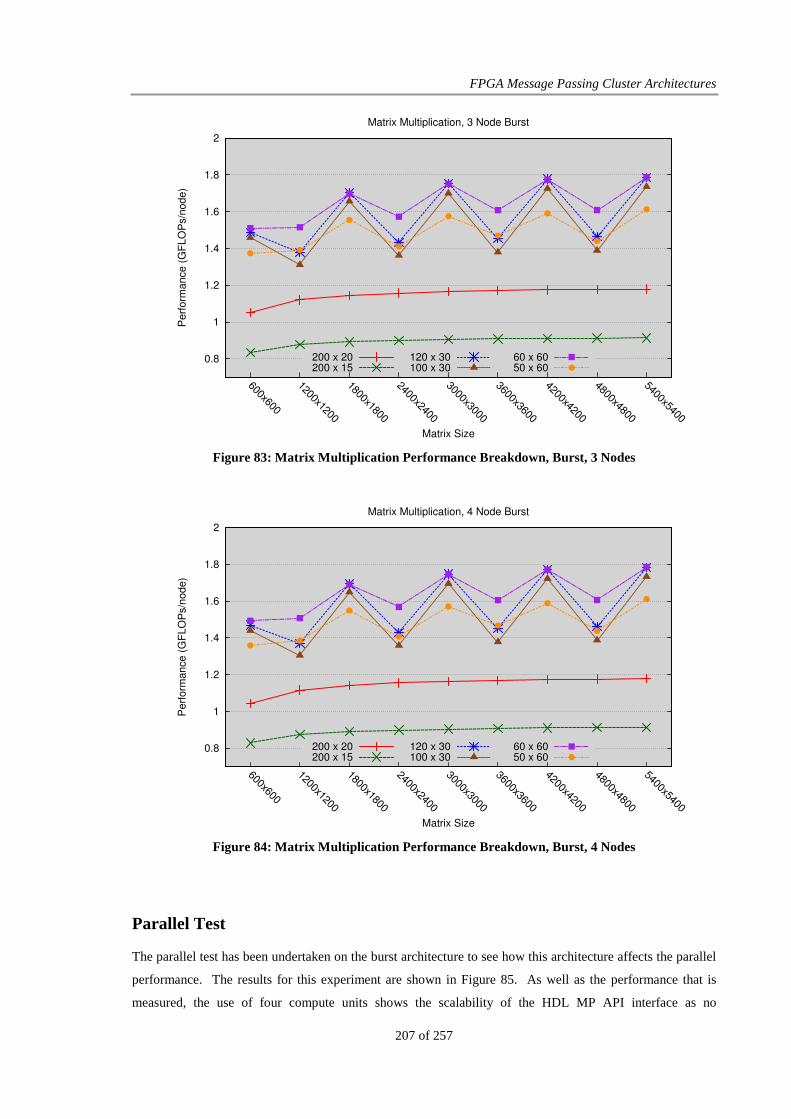
FPGA Message Passing Cluster Architectures
207 of 257
0.8
1
1.2
1.4
1.6
1.8
2
600x600
1200x1200
1800x1800
2400x2400
3000x3000
3600x3600
4200x4200
4800x4800
5400x5400
Perf
orm
ance (
GF
LO
Ps/n
ode)
Matrix Size
Matrix Multiplication, 3 Node Burst
200 x 20200 x 15
120 x 30100 x 30
60 x 6050 x 60
Figure 83: Matrix Multiplication Performance Breakd own, Burst, 3 Nodes
0.8
1
1.2
1.4
1.6
1.8
2
600x600
1200x1200
1800x1800
2400x2400
3000x3000
3600x3600
4200x4200
4800x4800
5400x5400
Perf
orm
ance (
GF
LO
Ps/n
ode)
Matrix Size
Matrix Multiplication, 4 Node Burst
200 x 20200 x 15
120 x 30100 x 30
60 x 6050 x 60
Figure 84: Matrix Multiplication Performance Breakd own, Burst, 4 Nodes
Parallel Test
The parallel test has been undertaken on the burst architecture to see how this architecture affects the parallel
performance. The results for this experiment are shown in Figure 85. As well as the performance that is
measured, the use of four compute units shows the scalability of the HDL MP API interface as no

Evaluation
208 of 257
modifications were performed on the hardware application microarchitecture to support the additional com-
pute units. The additional compute unit allows the parallel experiment to perform computations on a larger
data set, again showing scalability of the distributed hardware application microarchitectures and support for
the remote register transfer operations. From the results, running on a single compute unit, a time difference
of some 70 seconds is recorded, which is a performance improvement of approximately 30% over the non-
burst architecture. This level of performance increase is noted for all sizes, showing that the burst architec-
ture is better as would be expected but also that the HDL MP API application could operate correctly both for
burst and non-burst architecture approaches
Minimum Maximum
2 Node 1.66 1.99
3 Node 1.96 2.88
4 Node 1.90 3.57
The parallel test results measure performance improvements seen when additional nodes are used
for the computation. These results, in Table 30, show that each additional node improves the overall compu-
tational performance. The results for the minimum size are measured for the minimum matrix size and show
that the additional computation and remote register transfer overheads do not overlap efficiently with each
other to support the near linear improvement seen for the scaling test.
0
100
200
300
400
500
600600x600
1200x1200
1800x1800
2400x2400
3000x3000
3600x3600
4200x4200
4800x4800
5400x5400
6000x6000
6600x6600
7200x7200
7800x7800
8400x8400
9000x9000
9600x9600
10200x10200
10800x10800
11400x11400
Com
puta
tion T
ime (
seconds)
Matrix Size
Parallel Computation Times, Burst
1 Node FPGA2 Node FPGA3 Node FPGA4 Node FPGA
Figure 85: Parallel Matrix Multiplication Times, Bu rst
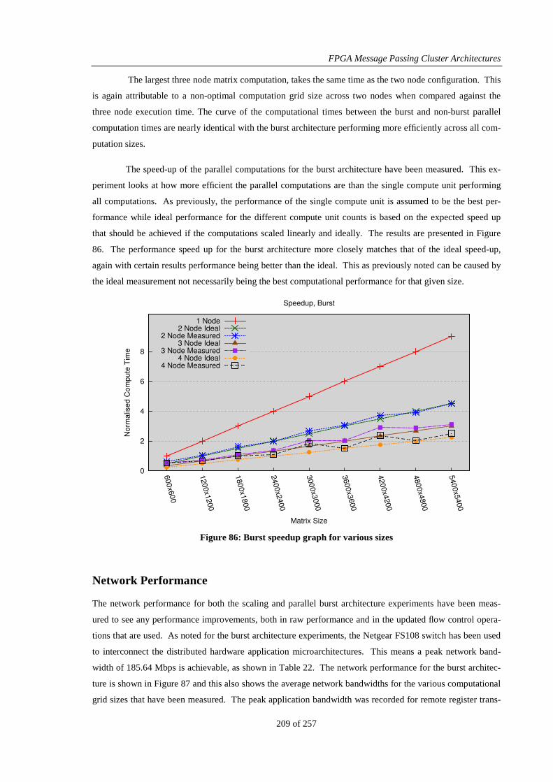
FPGA Message Passing Cluster Architectures
209 of 257
The largest three node matrix computation, takes the same time as the two node configuration. This
is again attributable to a non-optimal computation grid size across two nodes when compared against the
three node execution time. The curve of the computational times between the burst and non-burst parallel
computation times are nearly identical with the burst architecture performing more efficiently across all com-
putation sizes.
The speed-up of the parallel computations for the burst architecture have been measured. This ex-
periment looks at how more efficient the parallel computations are than the single compute unit performing
all computations. As previously, the performance of the single compute unit is assumed to be the best per-
formance while ideal performance for the different compute unit counts is based on the expected speed up
that should be achieved if the computations scaled linearly and ideally. The results are presented in Figure
86. The performance speed up for the burst architecture more closely matches that of the ideal speed-up,
again with certain results performance being better than the ideal. This as previously noted can be caused by
the ideal measurement not necessarily being the best computational performance for that given size.
0
2
4
6
8
600x600
1200x1200
1800x1800
2400x2400
3000x3000
3600x3600
4200x4200
4800x4800
5400x5400
Norm
alis
ed C
om
pute
Tim
e
Matrix Size
Speedup, Burst
1 Node2 Node Ideal
2 Node Measured3 Node Ideal
3 Node Measured4 Node Ideal
4 Node Measured
Figure 86: Burst speedup graph for various sizes
Network Performance
The network performance for both the scaling and parallel burst architecture experiments have been meas-
ured to see any performance improvements, both in raw performance and in the updated flow control opera-
tions that are used. As noted for the burst architecture experiments, the Netgear FS108 switch has been used
to interconnect the distributed hardware application microarchitectures. This means a peak network band-
width of 185.64 Mbps is achievable, as shown in Table 22. The network performance for the burst architec-
ture is shown in Figure 87 and this also shows the average network bandwidths for the various computational
grid sizes that have been measured. The peak application bandwidth was recorded for remote register trans-
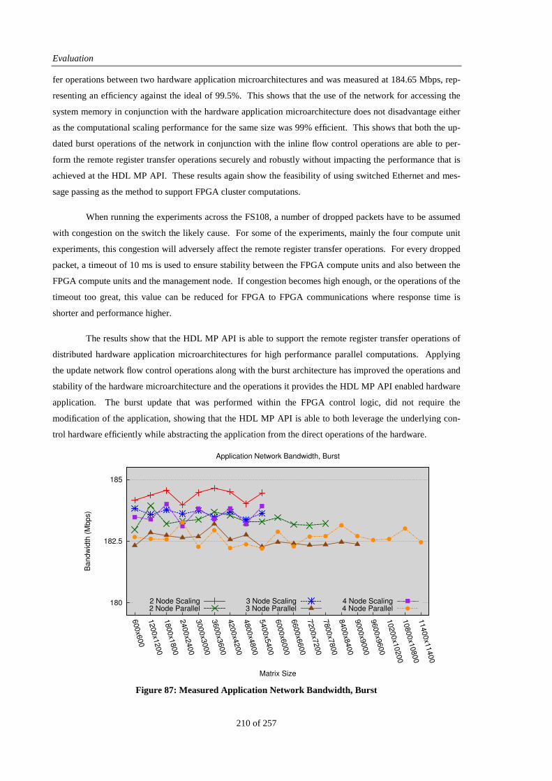
Evaluation
210 of 257
fer operations between two hardware application microarchitectures and was measured at 184.65 Mbps, rep-
resenting an efficiency against the ideal of 99.5%. This shows that the use of the network for accessing the
system memory in conjunction with the hardware application microarchitecture does not disadvantage either
as the computational scaling performance for the same size was 99% efficient. This shows that both the up-
dated burst operations of the network in conjunction with the inline flow control operations are able to per-
form the remote register transfer operations securely and robustly without impacting the performance that is
achieved at the HDL MP API. These results again show the feasibility of using switched Ethernet and mes-
sage passing as the method to support FPGA cluster computations.
When running the experiments across the FS108, a number of dropped packets have to be assumed
with congestion on the switch the likely cause. For some of the experiments, mainly the four compute unit
experiments, this congestion will adversely affect the remote register transfer operations. For every dropped
packet, a timeout of 10 ms is used to ensure stability between the FPGA compute units and also between the
FPGA compute units and the management node. If congestion becomes high enough, or the operations of the
timeout too great, this value can be reduced for FPGA to FPGA communications where response time is
shorter and performance higher.
The results show that the HDL MP API is able to support the remote register transfer operations of
distributed hardware application microarchitectures for high performance parallel computations. Applying
the update network flow control operations along with the burst architecture has improved the operations and
stability of the hardware microarchitecture and the operations it provides the HDL MP API enabled hardware
application. The burst update that was performed within the FPGA control logic, did not require the
modification of the application, showing that the HDL MP API is able to both leverage the underlying con-
trol hardware efficiently while abstracting the application from the direct operations of the hardware.
180
182.5
185
600x600
1200x1200
1800x1800
2400x2400
3000x3000
3600x3600
4200x4200
4800x4800
5400x5400
6000x6000
6600x6600
7200x7200
7800x7800
8400x8400
9000x9000
9600x9600
10200x10200
10800x10800
11400x11400
Bandw
idth
(M
bps)
Matrix Size
Application Network Bandwidth, Burst
2 Node Scaling2 Node Parallel
3 Node Scaling3 Node Parallel
4 Node Scaling4 Node Parallel
Figure 87: Measured Application Network Bandwidth, Burst
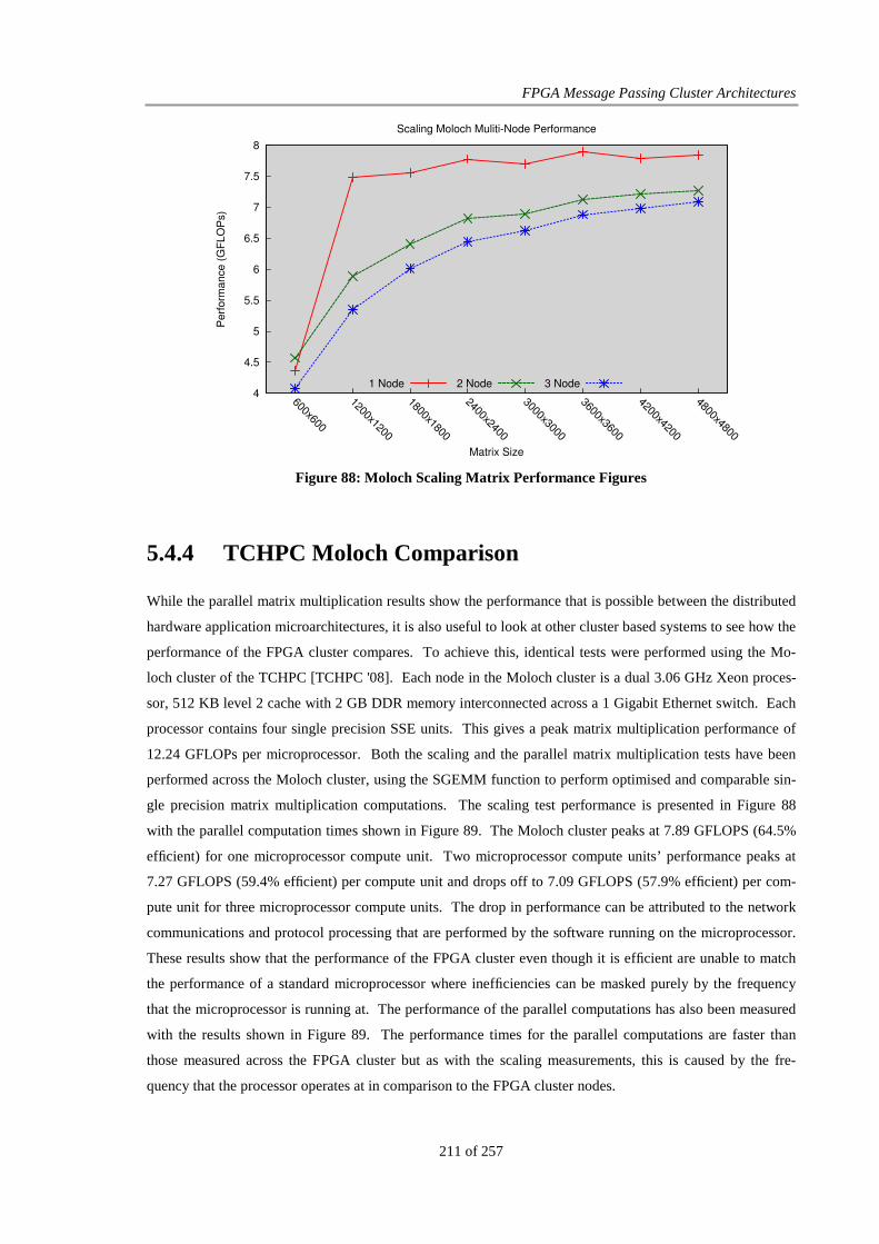
FPGA Message Passing Cluster Architectures
211 of 257
5.4.4 TCHPC Moloch Comparison
While the parallel matrix multiplication results show the performance that is possible between the distributed
hardware application microarchitectures, it is also useful to look at other cluster based systems to see how the
performance of the FPGA cluster compares. To achieve this, identical tests were performed using the Mo-
loch cluster of the TCHPC [TCHPC '08]. Each node in the Moloch cluster is a dual 3.06 GHz Xeon proces-
sor, 512 KB level 2 cache with 2 GB DDR memory interconnected across a 1 Gigabit Ethernet switch. Each
processor contains four single precision SSE units. This gives a peak matrix multiplication performance of
12.24 GFLOPs per microprocessor. Both the scaling and the parallel matrix multiplication tests have been
performed across the Moloch cluster, using the SGEMM function to perform optimised and comparable sin-
gle precision matrix multiplication computations. The scaling test performance is presented in Figure 88
with the parallel computation times shown in Figure 89. The Moloch cluster peaks at 7.89 GFLOPS (64.5%
efficient) for one microprocessor compute unit. Two microprocessor compute units’ performance peaks at
7.27 GFLOPS (59.4% efficient) per compute unit and drops off to 7.09 GFLOPS (57.9% efficient) per com-
pute unit for three microprocessor compute units. The drop in performance can be attributed to the network
communications and protocol processing that are performed by the software running on the microprocessor.
These results show that the performance of the FPGA cluster even though it is efficient are unable to match
the performance of a standard microprocessor where inefficiencies can be masked purely by the frequency
that the microprocessor is running at. The performance of the parallel computations has also been measured
with the results shown in Figure 89. The performance times for the parallel computations are faster than
those measured across the FPGA cluster but as with the scaling measurements, this is caused by the fre-
quency that the processor operates at in comparison to the FPGA cluster nodes.
4
4.5
5
5.5
6
6.5
7
7.5
8
600x600
1200x1200
1800x1800
2400x2400
3000x3000
3600x3600
4200x4200
4800x4800
Pe
rfo
rma
nce
(G
FL
OP
s)
Matrix Size
Scaling Moloch Muliti-Node Performance
1 Node 2 Node 3 Node
Figure 88: Moloch Scaling Matrix Performance Figures
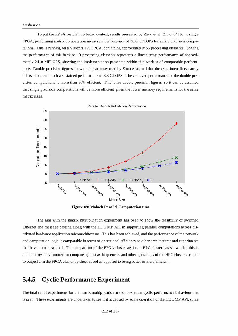
Evaluation
212 of 257
To put the FPGA results into better context, results presented by Zhuo et al [Zhuo '04] for a single
FPGA, performing matrix computation measure a performance of 26.6 GFLOPs for single precision compu-
tations. This is running on a Virtex2P125 FPGA, containing approximately 55 processing elements. Scaling
the performance of this back to 10 processing elements represents a linear array performance of approxi-
mately 2410 MFLOPS, showing the implementation presented within this work is of comparable perform-
ance. Double precision figures show the linear array used by Zhuo et al, and that the experiment linear array
is based on, can reach a sustained performance of 8.3 GLOPS. The achieved performance of the double pre-
cision computations is more than 60% efficient. This is for double precision figures, so it can be assumed
that single precision computations will be more efficient given the lower memory requirements for the same
matrix sizes.
The aim with the matrix multiplication experiment has been to show the feasibility of switched
Ethernet and message passing along with the HDL MP API in supporting parallel computations across dis-
tributed hardware application microarchitecture. This has been achieved, and the performance of the network
and computation logic is comparable in terms of operational efficiency to other architectures and experiments
that have been measured. The comparison of the FPGA cluster against a HPC cluster has shown that this is
an unfair test environment to compare against as frequencies and other operations of the HPC cluster are able
to outperform the FPGA cluster by sheer speed as opposed to being better or more efficient.
5.4.5 Cyclic Performance Experiment
The final set of experiments for the matrix multiplication are to look at the cyclic performance behaviour that
is seen. These experiments are undertaken to see if it is caused by some operation of the HDL MP API, some
-5
0
5
10
15
20
25
30
35
600x600
1200x1200
1800x1800
2400x2400
3000x3000
3600x3600
4200x4200
4800x4800
Com
puta
tion T
ime (
seconds)
Matrix Size
Parallel Moloch Muliti-Node Performance
1 Node 2 Node 3 Node
Figure 89: Moloch Parallel Computation time
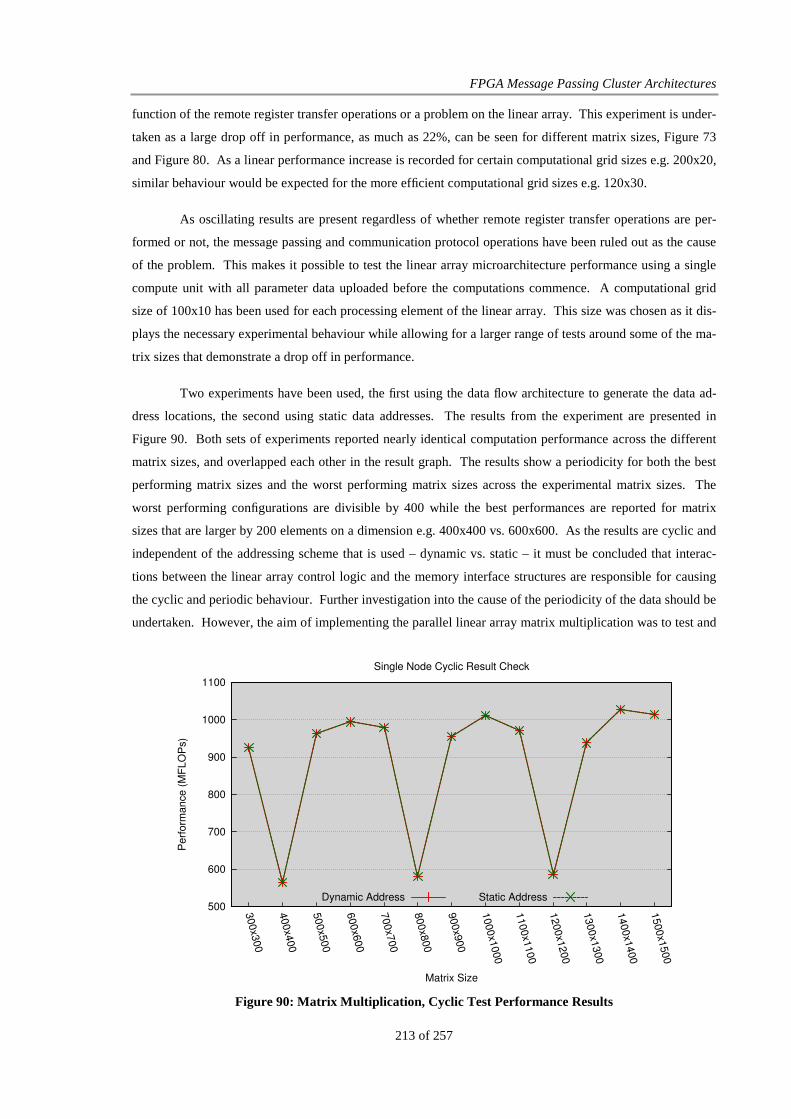
FPGA Message Passing Cluster Architectures
213 of 257
function of the remote register transfer operations or a problem on the linear array. This experiment is under-
taken as a large drop off in performance, as much as 22%, can be seen for different matrix sizes, Figure 73
and Figure 80. As a linear performance increase is recorded for certain computational grid sizes e.g. 200x20,
similar behaviour would be expected for the more efficient computational grid sizes e.g. 120x30.
As oscillating results are present regardless of whether remote register transfer operations are per-
formed or not, the message passing and communication protocol operations have been ruled out as the cause
of the problem. This makes it possible to test the linear array microarchitecture performance using a single
compute unit with all parameter data uploaded before the computations commence. A computational grid
size of 100x10 has been used for each processing element of the linear array. This size was chosen as it dis-
plays the necessary experimental behaviour while allowing for a larger range of tests around some of the ma-
trix sizes that demonstrate a drop off in performance.
Two experiments have been used, the first using the data flow architecture to generate the data ad-
dress locations, the second using static data addresses. The results from the experiment are presented in
Figure 90. Both sets of experiments reported nearly identical computation performance across the different
matrix sizes, and overlapped each other in the result graph. The results show a periodicity for both the best
performing matrix sizes and the worst performing matrix sizes across the experimental matrix sizes. The
worst performing configurations are divisible by 400 while the best performances are reported for matrix
sizes that are larger by 200 elements on a dimension e.g. 400x400 vs. 600x600. As the results are cyclic and
independent of the addressing scheme that is used – dynamic vs. static – it must be concluded that interac-
tions between the linear array control logic and the memory interface structures are responsible for causing
the cyclic and periodic behaviour. Further investigation into the cause of the periodicity of the data should be
undertaken. However, the aim of implementing the parallel linear array matrix multiplication was to test and
500
600
700
800
900
1000
1100
300x300
400x400
500x500
600x600
700x700
800x800
900x900
1000x1000
1100x1100
1200x1200
1300x1300
1400x1400
1500x1500
Perf
orm
ance (
MF
LO
Ps)
Matrix Size
Single Node Cyclic Result Check
Dynamic Address Static Address
Figure 90: Matrix Multiplication, Cyclic Test Perfo rmance Results

Evaluation
214 of 257
verify that the HDL MP API is able to support a distributed hardware application microarchitecture that is
performing remote register transfer operations as part of a parallel algorithm, which has been demonstrated
across a range of different experimental configurations.
As put forward by Bondhugula et al [Bondhugula '06] a strong cause of the oscillating behaviour
can be attributed to the memory access pattern. As they note, as the size approaches a power of 2 boundary,
cache line misses result in the loss of temporal locality as the memory interface buffer must be continuously
flushed and refilled with new data for every access. Changing the memory data layout would aid in removing
some of the oscillation behaviour. When this was applied by Bondhugula et al within their computation, a
performance improvement was recorded. A similar approach applied to the memory layout taking into ac-
count the block size would then improve and stabilise the achieved performance.
5.4.6 NAS Parallel Benchmark Discussion
Matrix multiplication has been presented to demonstrate the performance, feasibility and scalability of using
switched Ethernet and message passing in supporting parallel computing applications and the remote register
transfer operations between distributed hardware application microarchitectures. As part of the description
on the requirements of the HDL MP API the NPB were discussed and the characteristics of these applications
in conjunction with the benchmarks of the two approaches is now discussed.
Multigrid
Multigrid looks to arrive at a state of equilibrium/convergence when no changes arise across an entire set of
data in use for the computation. For correct performance, MG uses an iterative approach to calculating a
state of equilibrium with each new iteration getting closer to arriving at a result. Depending on the system
being measured, both two-dimensional and three-dimensional approaches are possible. When the algorithm
is parallelised across multiple computation elements, grid edge data needs to be exchange with neighbour
nodes to ensure all nodes are performing computations on the latest iterations data. It is possible to perform
the computations and the communications concurrently once edge data operations are performed first. The
amount of computations a node needs to perform to hide the communication is a function of the time it will
take to exchange the edge data between neighbour nodes. For switched Ethernet, the time to exchange small
amounts of data are higher than point-to-point links which will increase the amount of computations a node
will need to perform. This places a lower limit on the amount of computations which a node must perform.
For higher speed networks, with lower latencies, the computation lower limit will be smaller and this may
result in smaller FPGAs being possible against a switched Ethernet solution. Further MG exchanges data to
nearest neighbour nodes so a switched Ethernet network with its ability to exchange data as efficiently with
both near and distant nodes will not be an advantage, rather it is a disadvantage with higher latencies. Com-
paring the hardware and the software approaches, the lower communication time of the hardware approach
means it will be able to perform more efficiently on smaller computational grids by virtue of not requiring as
many computations to hide the communication overheads.

FPGA Message Passing Cluster Architectures
215 of 257
Conjugate Gradient
Conjugate Gradient solutions look to solve both sparse and dense linear systems which consist mainly of
matrix-vector computations using iterative methods. A CG solution occurs when the approximated vector
result has a low enough error associated with it such that it can be assumed to be the correct result. To per-
form the computations of a CG solver in parallel, both matrix-vector and matrix-matrix computations are
performed across all nodes, with data partitioning performed similar to that for parallel matrix multiplication
discussed previously [Jordan '02, Chen '04]. To perform the computations in parallel however, a mas-
ter/slave approach to data distribution and result accumulation is required. To improve the performance of
CG solvers on FPGAs, the matrix-vector and matrix-matrix computations can be efficiently implemented as
streaming microarchitectures but the overhead of communicating with a master node will slow the overall
computations that can be performed.
From the results above, it can be seen that the HDL MP API will support the matrix-matrix compu-
tations through the interface with sizes and overheads of various approaches already detailed. For the master
node, two approaches present themselves – use an FPGA which will require two implementation streams
(one for the master, one for the slaves) or to use the management node as the master. Overheads of exchang-
ing initialisation data with a management node provide details on the overheads that this incurs while also
showing that the FPGAs as slaves are able to interact with the management node as a master. With the com-
putations following a master/slave approach, no benefit will arise from the peer-to-peer data exchange per-
formance that has been measured between FPGAs, rather the overheads of performing the matrix-matrix
multiplication provide a per-node performance guide and the initialisation measurements provide approxi-
mate communication overheads that can be expected when exchanging data with it.
From the results, the size of data that should be computed on each FPGA should be large enough to
support the exchange of data across switched Ethernet while its directed communication structure will sup-
port the master/slave model by allowing direct master-slave communications. This compares to point-to-
point interconnects where data will is routed through all nodes to reach the master node. The memory band-
width and associated overheads of randomly accessing both matrix and vector data is also relevant as this
will influence the saturation that will be achieved on the computation logic. Again, the measurements of the
matrix multiplication show the performance that can be expected along with the memory bandwidth results.
These results show the size of systems that is readily solvable while the bandwidth measurements show the
lower bound of the time that can be expected for exchanging master/slave data. Combining these results, the
amount of data per node will need to be fairly large to benefit from the FPGA computation logic and mini-
mise the overheads that the data merging will introduce into the computations. From the different experi-
ment results though, the platform will be able to support the CG computations through the HDL MP API.
Fourier Transform
Fourier Transforms solve three-dimensional partial differential equations using parallel FFT. Parallel FFTs
require each node to both perform computations and data communications between nodes. Fourier Trans-

Evaluation
216 of 257
forms are implemented as iterative solvers, with a new iteration required for each new computation that
needs to be performed. Each iteration requires data to be exchanged between nodes such that the data comes
from nodes that are twice as distant as the previous iteration. Parallel FFTs perform two levels of parallel-
ism, on node parallelism which may perform a number of iterations followed by internode communications
to perform the final iterations. For this discussion, only internode communications will be looked at.
The internode communication pattern follows a butterfly pattern such that after each iteration, the
distance between communicating nodes doubles. The doubling of communication distance will result in in-
creased communication time for point-to-point networks as the hop distance increases however, for the
switched Ethernet in use here, there will not be an appreciable increase in communication time. This is seen
as the switched Ethernet interconnect does not introduce additional overheads based on the distance between
devices. This means that it is possible to know how long the communications will take in each iteration and
from this configure each node to perform an appropriate amount of computations. In parallel FFT, it is not
possible to overlap the computation and the communication operations, so knowing the time to exchange data
vs. the time to perform the computations will allow for a more tailored implementation that could be more
compute bound than communication bound. From the communication patterns that need to be supported in
parallel FFT, the HDL MP API will be able to support the changes in communication node easily, as demon-
strated in the barrier communication experiment where new iterations required new communication pairings
to be created. The latency overhead difference between the two approaches will make the hardware solution
more efficient on the communications but if the amount of computations against communications is large, the
communication approach that is taken will not influence the overall computation time.
The computation operations are also of interest as it is possible to perform a large amount of compu-
tations on an FPGA against needing increased numbers of communications. This additional parallelism in-
creases the resource usage of the FPGA however as the time to exchange data between nodes on switched
Ethernet does not change regardless of the communication distance8, it is easier to match the amount of com-
putation that a node should perform against the amount of available resources and also the number of nodes
that will be needed to perform the computation. From the results and also the available resources of each
FPGA, it could be expected that the size of FFT that can be performed across the system would be greater
than 10,000 points, while the use of external memory provides enough memory storage for even larger sizes
though the increased memory access will decrease the computation performance.
Integer Sort
Parallel integer sorting looks at how large (>500,000 integers) numbers of integers can be sorted efficiently
across many compute nodes at the same time. At the start of a parallel integer sort, each compute node has a
subset of the overall number of integers, which it sorts first. As the amount of data that is involved in an in-
teger sort is large, the use of external memory is a requirement with a large amount of data movement opera-
tions and temporary storage required to ensure the data is sorted correctly, while not corrupting unsorted data.
8 Once all communications occur across a single switch.

FPGA Message Passing Cluster Architectures
217 of 257
After a node has sorted its data, it exchanges the newly sorted data with its neighbour nodes. Each data ex-
change with neighbour nodes follows a point-to-point pattern with the amount of data to be exchanged de-
pends on the parallel sorting algorithm that is used.
Typical parallel integer sorting approaches exchange a large amount of data between nodes and
from the parallel matrix multiplication results, the HDL MP API easily supports the exchange of a large
amount of data. The overhead and expected time to exchange this can be seen from the parallel matrix mul-
tiplication communication times while the maximum performance times across the range of available net-
works are presented in the bandwidth experiments. Again, these experiments show that both the hardware
and software solutions are able to support a parallel integer sort while the DMA operations of the hardware
solution would be compatible with the large data exchanges that are seen from parallel integer sort. The is-
sue for parallel integer sort is not the data exchanges however, it is the performance of the FPGA in relation
to random memory address accesses and the storage structures that are required to perform the sorting opera-
tions. From the random access pattern that is present in parallel matrix multiplication, the HDL MP API will
be able to support these access patterns while the development of suitable hardware sorting solutions should
be feasible on the available FPGA resources.
A typical sorting operation is in the order of O(NlogN) operations while the amount of data to be
exchanged will be of the order O(N), making the sorting operations more costly than the communication op-
erations so either solution will be appropriate for performing the communication operations between distrib-
uted integer sorting hardware nodes. The sorting and communication operations can not be overlapped so the
use of efficient communication operations will help reduce the sorting times. The communication pattern
follows a nearest neighbour pattern so the benefit of the switched Ethernet in supporting both near and far
communications is not required. The communication latency overhead will not pose a problem as the
amount of data that may be exchanged will reduce this overhead to being a small proportion of the entire data
exchange time.
5.5 Ethernet Fragmentation Experiments
From the design, a new and novel method for performing Ethernet fragmentation to support arbitrary remote
register transfer sizes was presented in Section 3.2.4. The performance of this as conveyed in Figure 21 and
Figure 22 provided a performance advantage for padded packets. When this fragmentation approach was
implemented and experiments run on it to calculate the amount of performance improvement that was pre-
sent, a large difference was recorded between the approaches. As an improvement was seen, further testing
and experiments have been undertaken to see how the algorithm functions and behaves on a wider range of
architectures than those directly related to the research question.
As previously mentioned, fragmentation is required to allow for arbitrary sized remote register
transfer operations by distributed hardware application microarchitectures through the HDL MP API. Frag-
mentation is responsible for taking the message data and splitting it up so that the size of data transferred
Evaluation
218 of 257
between hardware application microarchitectures conforms with the underlying network’s MTU. As part of
the evaluation of the performance of the fragmentation algorithm, two additional experiment architectures
above the hardware communication microarchitecture and FPGA processor have been used. The first archi-
tecture extends the management node software so that two commodity PCs could be configured to exchange
data with each other. The second architecture modifies the network operations of the Linux Kernel – 2.6.27 –
to see if the fragmentation approach can function correctly as part of standard TCP internode communica-
tions and if so, does it also provide a performance advantage. This allows for an additional investigation into
how the fragmentation operates as part of an operational network. Two tests were conducted on each plat-
form, while an additional third test was feasible for the TCP/IP configuration:
Test 1: Two compute units exchange data using the split fragmentation algorithm.
Test 2: Typical fragmentation is used between the compute units, the data split as maximum size and re-
mainder.
Test 3: One compute unit is configured to use split fragmentation and the other to use typical fragmentation.
This configuration is only used with the TCP/IP tests.
The experiments see the use of a modified ping-pong experiment, similar to that used for the latency
and bandwidth experiments, with communication occurring between two interconnected nodes. A range of
message sizes have been used for the experiments, from one packet up to three packets with the focus of the
experiments on two packets. This focus is because the fragmentation is attempting to improve their perform-
ance, while one and three packet experiments look at how the performance scales in relation to different
packet counts. For the FPGA microarchitectures, data resides in Block RAM memory and is accessed
through the HDL MP API. For the commodity PC experiments, a user space array is generated and filled
with random data. The Linux tests use the ping application. For the commodity PC experiments, each node
consists of an Intel 2160 processor running at 1.8 GHz with 1 GB RAM.
5.5.1 FPGA Fragmentation Experiments
The first set of experiments are performed between distributed application hardware compute units. As frag-
mentation operations are transparent to the application running on the compute unit, the first step in the ex-
periment was identifying how the two approaches could be used independently and correctly. For the hard-
ware communication microarchitecture, this is achieved by using parameters which select whether to use
splitting hardware or not within the communication flow operations. Selecting between each requires resyn-
thesis of the hardware depending on the experiment but reduces the hardware resource usage against includ-
ing both structures on the FPGA logic. For the FPGA processor solution, a define compiler directive is used
which performs the same functionality as the hardware parameter. To select between each fragmentation
algorithm, a recompile is required. In keeping with the HDL MP API architecture, the same hardware appli-
cation microarchitecture is used for both the hardware and FPGA processor solutions, with the application
unaware which configuration it is operating with – split, typical or hardware, FPGA processor.
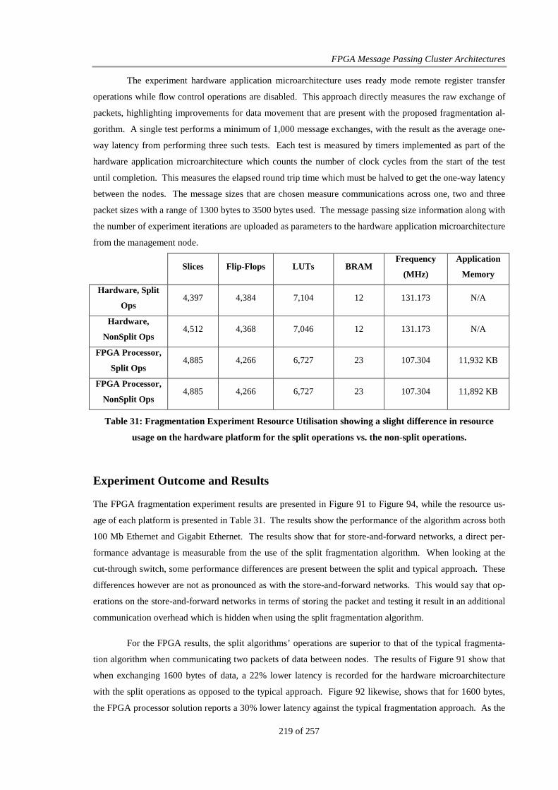
FPGA Message Passing Cluster Architectures
219 of 257
The experiment hardware application microarchitecture uses ready mode remote register transfer
operations while flow control operations are disabled. This approach directly measures the raw exchange of
packets, highlighting improvements for data movement that are present with the proposed fragmentation al-
gorithm. A single test performs a minimum of 1,000 message exchanges, with the result as the average one-
way latency from performing three such tests. Each test is measured by timers implemented as part of the
hardware application microarchitecture which counts the number of clock cycles from the start of the test
until completion. This measures the elapsed round trip time which must be halved to get the one-way latency
between the nodes. The message sizes that are chosen measure communications across one, two and three
packet sizes with a range of 1300 bytes to 3500 bytes used. The message passing size information along with
the number of experiment iterations are uploaded as parameters to the hardware application microarchitecture
from the management node.
Slices Flip-Flops LUTs BRAM Frequency
(MHz)
Application
Memory
Hardware, Split
Ops 4,397 4,384 7,104 12 131.173 N/A
Hardware,
NonSplit Ops 4,512 4,368 7,046 12 131.173 N/A
FPGA Processor,
Split Ops 4,885 4,266 6,727 23 107.304 11,932 KB
FPGA Processor,
NonSplit Ops 4,885 4,266 6,727 23 107.304 11,892 KB
Table 31: Fragmentation Experiment Resource Utilisation showing a slight difference in resource
usage on the hardware platform for the split operations vs. the non-split operations.
Experiment Outcome and Results
The FPGA fragmentation experiment results are presented in Figure 91 to Figure 94, while the resource us-
age of each platform is presented in Table 31. The results show the performance of the algorithm across both
100 Mb Ethernet and Gigabit Ethernet. The results show that for store-and-forward networks, a direct per-
formance advantage is measurable from the use of the split fragmentation algorithm. When looking at the
cut-through switch, some performance differences are present between the split and typical approach. These
differences however are not as pronounced as with the store-and-forward networks. This would say that op-
erations on the store-and-forward networks in terms of storing the packet and testing it result in an additional
communication overhead which is hidden when using the split fragmentation algorithm.
For the FPGA results, the split algorithms’ operations are superior to that of the typical fragmenta-
tion algorithm when communicating two packets of data between nodes. The results of Figure 91 show that
when exchanging 1600 bytes of data, a 22% lower latency is recorded for the hardware microarchitecture
with the split operations as opposed to the typical approach. Figure 92 likewise, shows that for 1600 bytes,
the FPGA processor solution reports a 30% lower latency against the typical fragmentation approach. As the
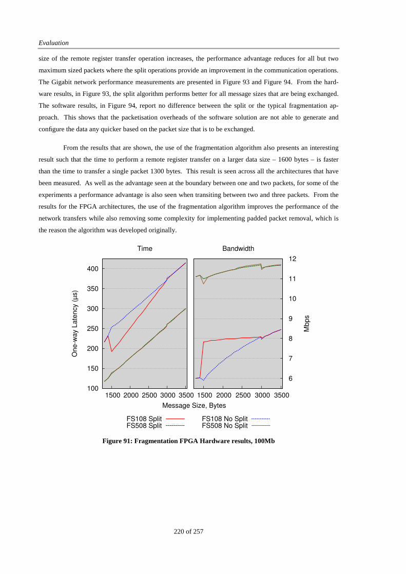
Evaluation
220 of 257
size of the remote register transfer operation increases, the performance advantage reduces for all but two
maximum sized packets where the split operations provide an improvement in the communication operations.
The Gigabit network performance measurements are presented in Figure 93 and Figure 94. From the hard-
ware results, in Figure 93, the split algorithm performs better for all message sizes that are being exchanged.
The software results, in Figure 94, report no difference between the split or the typical fragmentation ap-
proach. This shows that the packetisation overheads of the software solution are not able to generate and
configure the data any quicker based on the packet size that is to be exchanged.
From the results that are shown, the use of the fragmentation algorithm also presents an interesting
result such that the time to perform a remote register transfer on a larger data size – 1600 bytes – is faster
than the time to transfer a single packet 1300 bytes. This result is seen across all the architectures that have
been measured. As well as the advantage seen at the boundary between one and two packets, for some of the
experiments a performance advantage is also seen when transiting between two and three packets. From the
results for the FPGA architectures, the use of the fragmentation algorithm improves the performance of the
network transfers while also removing some complexity for implementing padded packet removal, which is
the reason the algorithm was developed originally.
100
150
200
250
300
350
400
1500 2000 2500 3000 3500
On
e-w
ay L
ate
ncy (
µs)
Message Size, Bytes
Time
FS108 SplitFS508 Split
1500 2000 2500 3000 3500
6
7
8
9
10
11
12
Mb
ps
Bandwidth
FS108 No SplitFS508 No Split
Figure 91: Fragmentation FPGA Hardware results, 100Mb

FPGA Message Passing Cluster Architectures
221 of 257
200
250
300
350
400
450
500
550
1500 2000 2500 3000 3500
One-w
ay L
ate
ncy (
µs)
Message Size, Bytes
Time
FS108 SplitFS508 Split
1500 2000 2500 3000 3500
4
5
6
7
8
Mbps
Bandwidth
FS108 No SplitFS508 No Split
Figure 92: Fragmentation FPGA Software results, 100Mb
20
25
30
35
40
45
1500 2000 2500 3000 3500
One-w
ay L
ate
ncy (
µs)
Message Size, Bytes
Time
GS608 SplitGS608 No Split
1500 2000 2500 3000 3500 50
55
60
65
70
75
80
85
Mbps
Bandwidth
GS608 SplitGS608 No Split
Figure 93: Fragmentation FPGA Hardware results, Gigabit
Evaluation
222 of 257
140
160
180
200
220
240
260
280
300
320
1500 2000 2500 3000 3500
One-w
ay L
ate
ncy (
µs)
Message Size, Bytes
Time
GS608 SplitGS608 No Split
1500 2000 2500 3000 3500 7.5
8
8.5
9
9.5
10
10.5
11
11.5
12
Mbps
Bandwidth
GS608 SplitGS608 No Split
Figure 94: Fragmentation FPGA Software results, Gigabit
5.5.2 PC Experiments
Extending the FPGA experiments, and using the management node code, the fragmentation algorithm has
been implemented to operate between commodity PCs. This test setup investigates how the algorithm per-
forms in the presence of an OS and to see does the same performance advantage reported for the FPGAs exist
between commodity computers. The management node code was updated to ensure it was able to function
between commodity PCs and as part of this, the node addresses were statically generated. This reduces ex-
periment implementation time and does not change the operations that are expected or measured – an initiali-
sation routine would not be timed.
The experiment is setup similar to the FPGA tests and measures the time to exchange a minimum of
1,000 packets between the compute units (PCs). The application operations are setup the same for the PC as
with the FPGA architectures. All communications use ready mode, without flow control operations imple-
mented. The PC experiment results are based on exchanging only normal Ethernet packets, limited to an
MTU of 1,500 bytes of data. Jumbo packets could not be configured to operate correctly and were not meas-
ured as part of the PC experiments. To measure the elapsed experiment time, the gettimeofday() function is
used, with the timer recording the time spent exchanging the 1,000 loops. The time is then averaged firstly to
generate a single round trip time and to then generate the one-way latency time. The GCC compiler, v4.4.0,
was used with varying optimisations applied as part of the experiments to see what effect compiler optimisa-
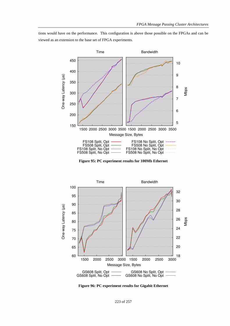
FPGA Message Passing Cluster Architectures
223 of 257
tions would have on the performance. This configuration is above those possible on the FPGAs and can be
viewed as an extension to the base set of FPGA experiments.
150
200
250
300
350
400
450
1500 2000 2500 3000 3500
One-w
ay L
ate
ncy (
µs)
Message Size, Bytes
Time
FS108 Split, OptFS508 Split, Opt
FS108 Split, No OptFS508 Split, No Opt
1500 2000 2500 3000 3500
5
6
7
8
9
10
Mbps
Bandwidth
FS108 No Split, OptFS508 No Split, Opt
FS108 No Split, No OptFS508 No Split, No Opt
Figure 95: PC experiment results for 100Mb Ethernet
60
65
70
75
80
85
90
95
100
1500 2000 2500 3000
One-w
ay L
ate
ncy (
µs)
Message Size, Bytes
Time
GS608 Split, OptGS608 Split, No Opt
1500 2000 2500 3000 18
20
22
24
26
28
30
32
Mbps
Bandwidth
GS608 No Split, OptGS608 No Split, No Opt
Figure 96: PC experiment results for Gigabit Ethernet
Evaluation
224 of 257
Experiment Outcome and Results
Figure 95 and Figure 96 present the PC experiment results. From the results, for all configurations, the frag-
mentation algorithm has a lower latency when exchanging the messages between the nodes. The result con-
figuration is similar to that of the FPGA nodes, showing that when no flow control is employed, the opera-
tions of the PC are similar to that of the FPGA architectures. Like the FPGA experiments, the performance
advantage is more evident on the store-and-forward switch. However, a performance difference is also re-
corded on the cut-through switch at smaller sizes. From the optimisation experiments that were performed,
the use of compiler optimisation level –O3 improves the communication performance, independently of the
fragmentation algorithm that is used. As with the FPGA architectures before it, there is a large change in
performance at the boundary between one and two packets. Again, the time to exchange a 1600 byte packet
as two individual packets is less than the time to exchange a 1300 byte packet. This leads to the belief that
the size of the packets being exchanged influences the performance, with certain sizes either easier to operate
and handle or design for.
5.5.3 Linux TCP Experiments
The final experimental configuration applies the split fragmentation algorithm to TCP/IP communications
performed between Linux computers. A number of different network configurations for the Linux experi-
ment were used, and these are discussed in more detail when describing those experiments. For the software
aspect of the experiments the same Linux setup was used, with the IP networking stack of Ubuntu Linux
8.10, kernel 2.6.27 modified to provide the desired functionality. The PC for the experiment consists of an
Intel 2160 processor running at 1.8 GHz with 1 GB RAM. The TCP/IP experiments measure the perform-
ance of the fragmentation algorithm in the presence of a complete flow control environment with tests run on
both a closed test network consisting of the experiment computers only and across an operational TCP/IP
network. This latter test is used to see how the split fragmentation algorithm interacts with compute units
that are not configured in a similar manner. As the operations are performed as part of TCP communications
no issues are expected with using the split fragmentation algorithm across an operational network.
The Linux Kernel implementation attempts to compare the performance when full TCP flow con-
trol operations are performed between the nodes. To reduce the complexity of implementing a TCP applica-
tion, standard ping which is included as part of Ubuntu 8.10 is used. Using ping as the application has meant
the test configuration has to be modified against that used for the previous experiments. Unlike the other
experiments which perform a single large communication iteration, the ping experiment performs a single
ping exchange which is performed multiple times. The time recorded for the ping experiments is that taken
from ping itself with the best and worst 15 times removed to reduce inconsistent communication perform-
ance. The times are then averaged, giving the overall time to exchange data using ping. The message size is
controlled through the ping ‘-s’ parameter option. The use of a pre-existing application also aids in showing
that the fragmentation strategy can be added without requiring modifications of pre-existing applications.

FPGA Message Passing Cluster Architectures
225 of 257
To update the TCP implementation to apply the split fragmentation algorithm, it was necessary to
identify where to implement the code modifications. This required identifying where fragmentation opera-
tions occur within the Linux Kernel and applying the split fragmentation algorithm. Difficulty identifying
exactly where fragmentation occurs has seen the implementation being placed on the slow_path operations
within the ip_fragment method of ip_output.c. To ensure the split fragmentation algorithm is used, the pre-
fragmented operations of ip_fragment are skipped although the application pre-fragmentation operations still
occur. This results in the TCP/IP implementation doubling up on the fragmentation operations that are per-
formed for the split algorithm against those of the typical non-split algorithm. From the results, this opera-
tion doubling up is reflected in a drop off in performance which will be discussed. As the networking opera-
tions of the Linux Kernel are integral to its correct operation, it was only possible to implement the algorithm
through a kernel rebuild. This means it is only possible to test and check the algorithm through rebooting
and loading the kernel version that is required.
The performed experiments can be grouped to give three overall test configurations. The first group
looks at the performance of the split fragmentation algorithm across an operational network, consisting solely
of Cisco switches and routers, with a 100 Mb interconnect and a Gigabit backbone between routers. For the
operational network experiment, data must be exchanged across two virtual LANs as well as routes between
2 different networks to reach the destination. The use of an operational network demonstrates the perform-
ance of the algorithm in a real network environment while highlighting the applicability of the approach in an
environment which is not under the experiments control. As the environment is not under the experiments
control, the results are for illustrative purposes as the same network data load can not be regenerated. This
experiment measured the time for two nodes to ping a common central network resource. To remove tran-
sient effects, both nodes commenced the ping operations concurrently so that similar network traffic was pre-
sent on the network for both compute units. The second group represent the standard tests that have been
undertaken by the previous experiments. These represent the fragmentation times when standard network
settings are used for both 100Mb and Gigabit Ethernet. The third group of results expand the scope of the
Gigabit tests and employ a range of Jumbo packets to see how they perform under the split fragmentation
algorithm.
Experiment Outcome and Results
The results of the operational, live network test are shown in Figure 97. Only two configurations were possi-
ble for the experiment, an unmodified configuration where typical fragmentation is used and a modified ver-
sion where split fragmentation is used. Within this experiment, a minimum of three store-and-forward hops
are present between the computer and the central resource. The computer is connected to a 100Mb network
with a Gigabit fibre backbone. The results show that for a wide range of the experiment sizes, the modified
kernel performs better. However, it does not perform better on all sizes with communication at 2400 bytes
being a packet size where the unmodified version performs better. From investigations into the configuration
of the network, the direct cause of this performance difference has not been ascertained. Possible causes of
this performance difference can be accounted for by the packet size of the unmodified solution being better

Evaluation
226 of 257
tuned to move through the network more efficiently or an unusual load on the modified node. The Ubuntu
platforms that are used have not been optimised for the experiments though extraneous applications have
been stopped as far as possible. For the unmodified system, the packet sizes across the network are 1460 and
940 bytes, while for the modified system, the packet sizes are 1200 bytes for both. Given the performance at
this point, speculation on the result would say that a packet size less than 1024 bytes might be able to traverse
the network more efficiently than packet sizes larger than it. For the modified results, this is the first sample
size which communicates packets which are greater than 1024 bytes. When both nodes are sending 2,800
bytes of data this represents two maximum sized TCP packets across the network with this reflected in both
configurations performing the same. The next result, 3,000 bytes is of interest as here, when three packets
are required, the modified version shows a marked improvement for sending this amount of data against the
unmodified version. This shows that the split fragmentation algorithm provides a direct performance advan-
tage against an unmodified version when run across an operational network. This experiment also shows that
the split fragmentation approach can be applied to an operational network without adverse affects.
1
1.05
1.1
1.15
1.2
1.25
1.3
1.35
1.4
1600 1800 2000 2200 2400 2600 2800 3000
On
e-w
ay L
ate
ncy (
ms)
Message Size, bytes
Fragmentation, Live 100Mb network
UnmodifiedModified
Figure 97: TCP/IP Fragmentation experiment, live 100Mb network
Figure 98 and Figure 99 show the results for the fragmentation experiments for both 100Mb and Gi-
gabit Ethernet. For both results, an MTU of 1500 bytes is used. The two nodes used for these experiments
were directly connected together across an appropriate network switch. This allowed for three test configura-
tions, two where both nodes were configured to use the same fragmentation algorithm and one where both
nodes used a different fragmentation strategy. This final configuration corresponds with the modified results
that are presented. This configuration gives an overview of how the split fragmentation would perform if
implemented on only a subset of the nodes of a network.

FPGA Message Passing Cluster Architectures
227 of 257
500
550
600
650
700
750
800
850
900
1600 1800 2000 2200 2400 2600 2800 3000
One-w
ay L
ate
ncy (
µs)
Message Size, bytes
Fragmentation, Closed 100Mb network
Both Unmodified1 Modified
Both Modified
Figure 98: TCP/IP Fragmentation experiments, closed 100Mb network
150
160
170
180
190
200
210
1600 1800 2000 2200 2400 2600 2800 3000
One-w
ay L
ate
ncy (
µs)
Message Size, bytes
Fragmentation, Closed 1000Mb network, 1500 MTU
Both Unmodified1 Modified
Both Modified
Figure 99: TCP/IP Fragmentation experiments, closed Gigabit network
The results from Figure 98, 100Mb Ethernet, are similar to those seen previously for the 100Mb
networks on the FPGA and custom communication PCs. The best performance is again seen with the split
fragmentation algorithm, with the worst performance recorded when neither node has been modified. The
mixed configuration performs between the two sets. Unlike in the live network experiment, the performance
of the different configurations do not converge on 2,800 bytes, rather they converge at 3,000 bytes which

Evaluation
228 of 257
requires three packets for its communication. Figure 99 shows the performance for the same configuration
when run across Gigabit Ethernet with a 1500 byte MTU. The results are a lot more unpredictable with no
one algorithm approach directly better than the other. For smaller sizes, the split fragmentation performs the
best while at larger sizes the non-split fragmentation algorithm achieves better performance. Some of the
cause of this relates to older underlying difficulties of a commodity PC in handling Gigabit rate network traf-
fic efficiently [Bellows '02]. From the results, the TCP experiment implementation adds to the communica-
tion overheads. The TCP split fragmentation approach still performs the pre-fragmentation operations which
are used by the unmodified system, before then also performing split fragmentation operations. For the re-
sults of Figure 99, this additional overhead coupled with the underlying difficulty of efficiently operating at
Gigabit speeds, the unmodified solution is able to achieve a better performance. The performance advantage
of the modified solution though at smaller packet sizes even with the additional copy operations still show
that the split fragmentation algorithm should operate more efficiently than the unmodified approach.
Extending the TCP experiments, the MTU of the Gigabit network was increased to examine algo-
rithm performance for different MTUs. Three sizes were selected, 5,000 bytes in Figure 100, 7,000 bytes in
Figure 101 and 9,000 bytes in Figure 102. These sizes aim to represent different configurations that may be
supported across a range of networks. The message sizes have equally been increased to reflect the new net-
work MTUs. From the graphed results, again the split fragmentation algorithm is more efficient at smaller
sizes, with these Gigabit results mirroring those of the FPGA, the PC and the 100Mb closed network experi-
ment. The performance of the split algorithm when communicating close to two maximum sized packets is
again not as good as the unmodified approaches. This is likely caused by the experimental nature of the im-
plementation and the operation doubling up that is performed within the modified version.
250
300
350
400
450
500
550
600
6000 8000 10000 12000 14000
One-w
ay L
ate
ncy (
µs)
Message Size, bytes
Fragmentation, Closed 1000Mb network, 5000 MTU
Both Unmodified1 Modified
Both Modified
Figure 100: TCP/IP Fragmentation experiments, closed Gigabit network, MTU 5000

FPGA Message Passing Cluster Architectures
229 of 257
350
400
450
500
550
600
650
7000 8000 9000 10000 11000 12000 13000 14000
One-w
ay L
ate
ncy (
µs)
Message Size, bytes
Fragmentation, Closed 1000Mb network, 7000 MTU
Unmodified1 Modified
Both Modified
Figure 101: TCP/IP Fragmentation experiments, closed Gigabit network, MTU 7000
400
450
500
550
600
650
700
750
800
850
10000 12000 14000 16000 18000 20000
One-w
ay L
ate
ncy (
µs)
Message Size, bytes
Fragmentation, Closed 1000Mb network, 9000 MTU
Unmodified1 Modified
Both Modified
Figure 102: TCP/IP Fragmentation experiments, closed Gigabit network, MTU 9000
5.5.4 Fragmentation Experiment Discussion
The split fragmentation algorithm proposed in Section 3.2.4 has been tested in a wide range of experimental
environments. The results show that the split fragmentation algorithm provides a marked improvement in
Evaluation
230 of 257
packet communications as seen firstly by the reduced times to send the same size packets and secondly when
it is possible to send a larger data size consisting of two packets faster than a single packet. While the algo-
rithm shows performance advantages, this was not replicated across all experiments with the TCP implemen-
tation not always reporting an advantage. This arises because of the experimental nature of the implementa-
tion as opposed to any fault in the algorithm itself.
The experiments have looked at the fragmentation operations from a high level view – fragmenta-
tion has to be performed and here is an algorithm to perform it. To put the measured results into context,
different applications which would benefit from the fragmentation algorithm are now presented. The identi-
fied applications are those where a majority of the communication data would fall between 1,000 and 4,000
bytes as a range where the split fragmentation algorithm has demonstrated performance advantages. The use
of jumbo packets for this are not explored as from the results, an MTU of 5,000 bytes already performs in a
single communication what a standard MTU would take 4 packets to communicate. The work of Vetter et al
[Vetter '03], Cypher et al [Cypher '93], and Sur et al [Sur '06] look at different applications and their commu-
nication requirements. As part of the results discussion, we look at different applications they present and the
performance advantage that might be possible.
From Vetter et al [Vetter '03], the Structured Adaptive Mesh Refinement Application Infrastructure
(SAMRAI) application would benefit from the use of the split fragmentation algorithm as 34% of the data
communications require between 2,048 and 4,096 bytes with approximately 70% of all communications re-
quiring between 1,024 and 8,196 bytes. The amount of message communications performed is dependant on
the number of tasks used by the application with a range of between 43 and 136 message communications
performed. Cypher et al [Cypher '93] look at different applications, where a wider range of suitable applica-
tions are covered. Included in these applications are 2D and 3D fluid flow simulations, with 100% (29,147)
and 12.8% (8,188) of the communications for each falling between 1K and 8K bytes respectively. For the
3D fluid flow simulations, communications in the 1K to 8K range represent the upper communication sizes,
although some very large message communications are also performed with 108 communications between
512K and 4M. These would most likely represent data distribution operations as opposed to computation
communications. Molecular Dynamics has also been identified as an application with a large portion, 33%
(15,019), of data communication within the 1K to 8K bracket. Unlike the 3D fluid flow however, these
communications represent the lower range of the application’s requirements. A chemical reaction simulation
which applies first principles to see how quantum chemical reactions behave performs 15% of its communi-
cation in this range, totalling 68 communications. For the chemical reaction simulation however, the major-
ity of communications are between 8K and 64K in size. Finally, a climate simulation application performs
15%, some 101,376 communications which exchange the given range (1K – 8K), with no communications of
larger data required. Three other applications reported by Cypher are not detailed here as their communica-
tion pattern would not suit the split fragmentations operations as they either perform no communications in
the necessary range or all communications are too large. Sur et al [Sur '06] investigate the communication
requirements of the NPB. From the results that they present, only the MG application performs any commu-

FPGA Message Passing Cluster Architectures
231 of 257
nications requiring between 1K and 4K byte messages. The other applications either perform smaller or lar-
ger message sized communications.
The results and discussion show that the split fragmentation algorithm aids in reducing communica-
tion latency and with the details from the application investigations, a wide range of applications exist that
could benefit from this performance advantage.
5.6 Evaluation Conclusions
The evaluation experiments have set out to test and measure if using switched Ethernet and message passing
is a realistic, feasible and scalable approach for interconnecting distributed hardware application microarchi-
tectures implemented on FPGAs. Experiments have looked at the performance of the HDL MP API in sup-
porting algorithm parallelisation along with the architectures that support the remote register transfer opera-
tions – the hardware communication microarchitecture and the FPGA processor architecture. A range of
aspects of each approach, to support the remote register transfer have been tested. These experiments have
looked at how the HDL MP API provides a hardware application microarchitecture access to a message pass-
ing protocol for exchanging data between arbitrary point-to-point remote register transfers and collective
communications. Finally, the use of the HDL MP API to abstract the implementation of the communication
interconnect from a high performance parallel application has also been performed. These experiments re-
enforce the requirement to support remote register transfer between distributed hardware application mi-
croarchitectures which can be located on a diverse number of FPGAs. Support for remote register transfer
operations provides an algorithm with the ability to scale across additional reconfigurable logic, allowing the
algorithm to meet increased computation requirements. Along with identifying the need to support an ab-
stract interface for remote register transfer operations, the results also show that when performance is com-
pared with the MGT based approaches, that switched Ethernet represents a sensible approach for intercon-
necting distributed FPGAs. This is seen as the overall remote register transfer performance along with the
ability to easily add and remove nodes represents a scalable approach which has not be demonstrated by the
MGT based solutions to interconnecting FPGAs. The ability to mix the interconnect structures and devel-
opment boards shows that switched Ethernet is able to support a diverse range of operational structures with
the speed of data exchange a function of the interconnect approach that is used. This style of operation has
not been demonstrated robustly by others. A further advantage of switched Ethernet is the scalability and
robustness of the interconnects that are employed. While scalability has been demonstrated through various
experiments – barrier, initialisation, parallel matrix multiplication – the robustness of the solution has been
measured through the various development boards that can be used with each other and a management node
in support of application parallelisation through the fork-join approach.
The experiments have used a hardware communication microarchitecture and a soft-core FPGA
processor to measure the performance and operations of the remote register transfers. From the various ex-
periment results, the hardware communication microarchitecture provides the best performance for support-
ing the remote register transfer operations between the distributed hardware application microarchitectures.
Evaluation
232 of 257
This is seen as the hardware communication microarchitecture provides the best interconnect performance
with the lowest latency. When looking at the reconfigurable resource usage, the hardware communication
microarchitecture also has a smaller footprint using fewer slices and fewer Block RAMs making more avail-
able for an application to use for temporary computation data storage. The reduced Block RAM usage re-
flects the dedicated nature of the hardware communication microarchitecture with all operations supported
through logic while the FPGA processor requires software stored in memory to function. While the size of
the software is minimised, additional Block RAMs are still required to support the FPGA processor message
passing and communication functionality.
From the experiments, further information can be learnt about the message passing and communica-
tion protocols that have been developed. Through the use of a customised data packet, overheads associated
with packet identification have been kept to a minimum with network performance for 100 Mb Ethernet
nearly able to achieve maximum performance. For the operation of the message passing and transport proto-
cols for exchanging application data, a large overhead is apparent for small data sizes on each approach, with
the request-to-send/clear-to-send reducing the achieved performance. This is seen in the low performance
measurements from the bandwidth experiments but also in the high, when compared to MGT approaches,
latency for exchanging minimum sized packets. As the amount of data that needs to be transmitted increases,
the overhead of the initial handshake is no longer a concern as reflected in the amount of network bandwidth
an application is able to access.
Comparing both the hardware and the software approaches, a number of architectural differences af-
ford the hardware approach better overall performance. For the hardware approach, the ability to test and
operate on data as it arrives at the interface along with packet generation as it is communicated reduces the
amount of operations that need to be performed on the data. This is reflected in the communication protocol
where an error with a packet can be identified early and no further operations performed on that packets data.
Through these operations, the hardware approach is able to support DMA transfers. Comparing these opera-
tions with the software approach, data copy operations along with packet building operations on the proces-
sor are required while packets can only be identified after they have been stored in intermediate memory
buffers. This increases the overheads in moving data between the application microarchitecture and the in-
terconnect, resulting in a lower overall performance. To correctly exchange the data however, these opera-
tions can not be avoided. One of the major implementation difference that allows the hardware operate more
efficiently can be seen with the control packet exchange operations where the hardware is able to test and
operate on the data before the packet is completely received while the software must wait for the packet to be
received and moved to intermediate memory before it can be tested to know what operations to perform.
Along with packet data operations, the hardware approach employs an efficient interrupt handling and control
structure which allows for concurrent processing of both transmit and receive operations. This is not possible
with the software approach where a polling operation is used to ensure correct identification and operation of
packets through the network. This again represents a performance difference between each approach as the
hardware is able to operate concurrently on the network data while the software must sequentially deal with
network events.

FPGA Message Passing Cluster Architectures
233 of 257
While the hardware communication microarchitecture and software FPGA processor perform the
data communications, the HDL MP API enables the abstraction of these operations from the hardware appli-
cation microarchitectures and these have been tested. As part of the evaluation, parallel matrix multiplication
has been undertaken to evaluate the HDL MP APIs support for high performance parallel computations dis-
tributed across hardware application microarchitectures operating on different FPGAs. Results from the par-
allel application showed that the HDL MP API supports high performance parallel algorithms while as dis-
cussed, the HDL MP API allows the implementation system to be updated while the application logic was
not changed. This was seen with the update to the burst interface operations and the updated network flow
control operations. The HDL MP API also provided scalability operations through the ability to include or
not different collective communications and support of a single FPGA computation image regardless of the
number of FPGAs that were employed for experiments.


235 of 257
Chapter 6
Conclusions and Future Work
This thesis has set out to investigate the feasibility of using message passing to support the exchange of data
between distributed hardware application microarchitectures across a switched Ethernet interconnect. As
part of this investigation, a hardware application interface, the HDL MP API, to support remote register
transfer operations between independent application microarchitectures which are performing the computa-
tions of a parallel algorithm has been developed. From the experiments that have been performed to evaluate
the research question, the following conclusions can be made:
• Message Passing between distributed hardware applications across a switched Ethernet network is
a feasible approach to use, as shown by the network performance that has been achieved and sup-
port for a high performance application, parallel matrix multiplication.
• Through the use of a hardware abstraction interface, the HDL MP API, both hardware and soft-
ware message passing and communication operations are feasible for supporting parallel computa-
tions. Of these approaches, the hardware approach is more practical as it supports lower commu-
nication latency, higher network performance and some additional operations not readily sup-
ported by a software approach e.g. DMA operations
• Through the experiments that have been performed, it has been possible to compare this approach
to other related solutions to help answer the research question. Performance has been similar
while the use of a single interconnect across all computation devices facilitates a robust and scal-
able approach for supporting computation parallelisation.
• The HDL MP API while abstracting the implementation approach has also aided in comparing the
hardware and software approaches as the it was possible to use the same application independent
of the manner used to exchange data. The HDL MP API also facilitated parametric communica-
tions as different collective communications could be easily supported while not impacting other
applications which did not require them.

Conclusions and Future Work
236 of 257
The HDL MP API allows the hardware application microarchitectures to be implemented independ-
ently of the message passing and communication operations that are used. This has been demonstrated with
the parallel matrix multiplication where on-chip parallelisation operations were extended across multiple
interconnected and distributed FPGAs while further shown with the range of benchmark experiments which
were undertaken to measure overall system performance. As part of these experiments, the scalability of the
platform has been tested through the use of both, the matrix multiplication computations and the additional
tests which show the use of multiple interconnected FPGA nodes across the Ethernet switches. This scalabil-
ity has been supported directly by the HDL MP API. Scalability has also been shown through the program-
mability of the HDL MP API where additional communications could be easily added, with collective com-
munications used to demonstrate this. Additional communications could be implemented without modifying
pre-existing applications as the additional communications are supported through the HDL MP API. This
demonstrates the benefit of a single command interface which will support the remote register transfer opera-
tions easily and directly without requiring modifications of pre-existing code basis. Rather, it allows im-
provement in the performance of applications while not impacting their performance if the communications
are not required.
For each architecture, the exchange of register data between microarchitectures has required the de-
velopment and implementation of both a message passing and communication protocol. These protocols
have been developed to support the scalable and robust transfer of data between the distributed hardware
application microarchitectures. Through the use of the HDL MP API, the user is abstracted from the physical
operations of the protocols but the requirements and operations of the protocols for supporting this are still
required from the implementation perspective. The design and development of these protocols firstly facili-
tate the exchange of remote register transfer operations through the use of the messages while the communi-
cation protocol ensures the correct exchange of data across the switched Ethernet interconnect. From the
structures possible for implementing message passing, a layered approach has been taken which has seen the
message passing operations implemented independently of the interconnect that is used. The message pass-
ing protocol functions of send and receive accept application communication requests and direct the inter-
connect control hardware to perform the handshake and data exchange operations. The communication pro-
tocol has been developed to provide packet-based communications across switched Ethernet. The use of this
communication protocol in conjunction with Ethernet switches allows for scalability of the available applica-
tion hardware resources. The communication protocol that has been developed for this work shows that a
specific protocol in a controlled network structure is able to operate efficiently and maintain correct commu-
nications between interconnected nodes. As part of the communication protocol development a novel means
to exchange data across store-and-forward networks has been identified. This algorithm approach does not
display the see-saw behaviour between packets that are typically seen when exchanging data. This operation
has also shown a performance advantage over a typical IP approach to exchanging data. The benefit of this
algorithm is that it reduces the communication overheads between interconnected nodes, reducing the time
spent communicating data. During the discussion on the fragmentation algorithm results, details on a number
of applications which would benefit from the use of this algorithm have been presented.

FPGA Message Passing Cluster Architectures
237 of 257
Through the use of switched Ethernet and message passing, a novel aspect of the work has been the
ability to mix and match the FPGA development boards that support the distributed application. The use of
Ethernet also removes the need for an interconnect bridge between the computation resources of the FPGAs
and a management compute unit which aids in reducing the cost of implementing the FPGA hardware archi-
tectures and also furthers support for the fork-join approach to application parallelisation.
From the experiment results, the following additional information can be developed, that there is a
need to match up the interconnect that is supported with the hardware that is being used. In the background
chapter, a number of projects are detailed which use FPGA processors to support the exchange of data be-
tween distributed FPGAs through the use of high performance interconnects – MGT point-to-point links.
Results in this thesis show that the performance of the interconnect may not be a bottleneck and that incur-
ring the additional costs of a higher specification interconnect may not provide any advantage to the data ex-
change operations. This is evident where the difference in FPGA processor bandwidth between the 100 Mb
and Gigabit Ethernet was approximately 5 Mbps. The overheads of supporting the software operations show
that it is not overly advantageous for the remote register transfer operations of a distributed hardware applica-
tion microarchitecture to use a high performance interconnect.
6.1 Limitations
While developing the HDL MP API and remote register transfer logic, certain limitations are identified that
have not been addressed within the implementation of this work. Investigating these limitations from the
HDL MP API and working down to the physical interconnect interface, the first limitation concerns the op-
erations of the collective communications. For the present implementation of the collective operations, all
data regardless of the destination node is transferred across the network. This is a costly copy operation if
both the source and destination node are the same device. To address this limitation, rather than moving data
between the application registers and the network, support for moving data between registers on the same
device would be required. The HDL MP API interface already supports the necessary interface signals
meaning the update is only applicable to the implementation approach, and not the HDL MP API. Address-
ing this concern would reduce the time to move data as part of a collective communication.
While the HDL MP API supports remote register transfer operations, it only supports a single com-
munication at a time. This means a remote register transfer operation must complete before starting the next
one. Message passing queues have been developed to support multiple outstanding communications concur-
rently. These have been simulated to show correct functionality but have not been implemented on the hard-
ware. As these queues were not required for experiments, simulations were enough to show they operated as
required. These queues would need to be tested on the hardware to ensure they are able to support multiple
communications. Support for multiple communications simultaneously would mirror the non-blocking op-
erations of MPI where it is possible to perform communication and computation at the same time. With the
use of a hardware application microarchitecture both the communication and computations will occur simul-
taneously on the same hardware, regardless of whether blocking or non-blocking communications are used.

Conclusions and Future Work
238 of 257
While the communication protocol supports the exchange of data between interconnected FPGAs
across switched Ethernet, some limitations have been identified with the implementation. When developing
the synchronisation communications, certain assumptions about the stability of switched Ethernet were made.
This has resulted in the synchronisation packets being generated but not acknowledge as per the exchange of
data packets. Under heavy communication loads, the use of this approach for synchronisation does not work
as packets can be dropped because of congestion. This issue can be resolved by adding dedicated flow con-
trol logic as part of the hardware communication microarchitecture and by adding additional software for the
FPGA processor to support the synchronisation flow control operations. Maintaining dedicated flow control
structures is more advantageous as it reduces delays on the interconnect while also supporting the fact that
synchronisation packets can be received at any time during an applications execution. As part of the com-
munication protocol, dropped packets will arise and to identify these, a timeout along with the packet number
are used. The timeout value is set artificially high to support communications between the FPGA nodes and
the management node. It should be possible to use a variable length timeout based on the nodes that are ex-
changing data – one timeout for between FPGAs, a different time out for between the FPGA and manage-
ment node. Packetisation operations see all packets created after the previous data has been sent. This re-
duces network bandwidth as no overlap of communication and data packetisation is performed. This sees
reduced network performance on Gigabit Ethernet while necessitating the disabling of the transmission wa-
termark as part of the experiments to show good performance. By using packet pre-buffering operations like
those mentioned, it is expected that the watermark can be re-enabled while better bandwidth performance
figures are also expected.
The FPGA processor solution has been implemented to support the research question. This means
that it has been developed for the various experiments that it was used for and is not a complete, robust solu-
tion for supporting remote register transfer operations. This can be seen as no flow control operations are
used, however the packets are generated correctly – headers and counters are implemented and prepended
appropriately. This limitation does affect the amount of memory that is needed for the software communica-
tions but does not affect other aspects of the results that have been recorded and presented.
A final limitation relates to the interoperatibility of the hardware communication microarchitecture
and the FPGA processor. While the HDL MP API does support parallel computations across distributed
hardware application microarchitectures, certain implementation decisions and differences between the two
architectures mean it is not possible to use them both as part of the same computations, rather all computation
resources must use the same communication structures. This limitation arises because of the synchronisation
operations that are performed as part of the hardware approach. For the hardware, it is possible to test pack-
ets as they arrive at the network interface. This allows for early packet testing and results in the addition of
the embedded CRC as part of the synchronisation packets. This results in reduced latency and implementa-
tion complexity for the hardware. However, while this improves hardware latencies, implementing the CRC
as part of the FPGA processor solution is not necessary. In the FPGA processor solution, the Ethernet CRC
packet is tested and checked before the synchronisation data is tested. As only a correct packet will be re-
ceived, no additional benefit arises from the embedded CRC value. This difference in implementation pre-

FPGA Message Passing Cluster Architectures
239 of 257
vents the two architecture approaches from working with each other. Solutions are either to remove the em-
bedded CRC aspect from the hardware approach or implement the CRC embedding with the FPGA proces-
sor. Because of the overheads of implementing the CRC embedding operations on the software, the best so-
lution is to remove the embedded CRC value and only use the Ethernet CRC value.
6.2 Future Work
Some of the limitations highlight future work that can be taken with the research and architectures that have
been designed and implemented in this work. This section looks at some of the future work that could be
undertaken. Again, following the flow from the thesis, the details now are based on looking from the HDL
MP API interface down through the implementations.
While matrix multiplication has been able to prove the operations of the HDL MP API in supporting
distributed hardware application microarchitectures, testing using other applications should be undertaken.
From the background, possible other applications are Fast Fourier Transform, Multigrid computations (heat
exchange) or Conjugate Gradient problems. Each has been shown to work on an FPGA while details on par-
allel implementations are readily available and detailed in this thesis.
The HDL MP API is designed with a single communication command interface. What this means is
that a new communication operation can only be started once previous ones have finished. While this inter-
face supports collective communications easily, the ability to perform multiple communications simultane-
ously is not present in this approach. While message queues look to address this, it still requires the applica-
tion microarchitecture to pipeline the communication requests. By using multiple independent remote regis-
ter transfer interface ports, this requirement would be removed and it would be possible to request multiple
communications simultaneously.
Matrix multiplication experiments highlight an issue with the memory interface in terms of the cy-
clic performance of the computations. The cause of this should be further investigated to see what part of the
memory architecture is causing the problem and can it be removed or fixed. As well as this aspect of the
memory interface, a further concern is the interfacing of DDR memory with Gigabit Ethernet. Calculations
show it is not possible in the memory controllers present architecture to support Gigabit data rates, though it
should be possible to implement and test the Gigabit remote register transfer operations between DDR
memories.
For network operations, packet pre-buffering support should be added as part of the packetisation
operations. While packet pre-buffering was not required with the 100 Mb Ethernet experiments, it quickly
became apparent it was needed with Gigabit Ethernet to support the high rate of communications. Imple-
mentation of this should be undertaken to allow for the transmission watermark along with interfacing DDR
memory with the network control logic.
Conclusions and Future Work
240 of 257
The FPGA processor implementation and experiments can be further refined and updated. While
looking at the MicroBlaze processor, it has become apparent that it does not support burst data transfer opera-
tions. This is one cause for the difference in performance between the two solutions. To resolve this con-
cern, a different processor should be used as part of the FPGA processor implementation, with one such
processor the PowerPC already supported by the development tools. The PowerPC is an embedded proces-
sor on the FPGA and its use for remote register transfer operations should be investigated. The use of this
processor will have an impact on the reconfigurable resource usage as very few resources are consumed sup-
porting this processor against the need to support the MicroBlaze processor on the FPGA.
Along with looking at the PowerPC processor, a further refinement that would support remote regis-
ter transfer operations is to use the FPGA processor to setup and control the structures while hardware is used
to perform specific operations on the data and packet testing. This hybrid solution would look to get the ease
of implementing an efficient solution without some of the implementation overheads that are introduced in-
cluding complexity cost and verification overheads. While a hybrid approach could reduce some of the im-
plementation complexity, its overall logic usage would be higher than either the FPGA processor or dedi-
cated hardware communication microarchitecture as operations from both are merged without the ability to
reduce the amount of resources required by the FPGA processor any further.
241 of 257
Appendix A FPGAs
Field Programmable Gate Arrays are Integrated Circuits that allow for hardware levels of parallelism while
retaining software levels of reconfigurability. This is achieved through the technology that makes up the
FPGA, the slice logic.
A.1 Compute Resources
The basic operation of an FPGA is to run the desired binary operations defined by HDL code. In a standard
system, this operation would be performed by creating the necessary gate structures and interconnecting them
together. However, to allow the FPGA to be completely reconfigurable, using static gates would not provide
for the desired functionality. Rather, the basic logic elements of an FPGA design are provided by Look Up
Tables, which, based on the inputs, generate the appropriate output. All operations can be defined through
the use of the LUTs however, timing and other configuration considerations have seen the addition of dedi-
cated hardware as part of the slice logic. The carry chain logic is used for performing arithmetic operations
including comparison operations. The carry chain has been developed to use dedicated interconnects be-
tween the units which reduces the time when multiple units are cascaded together. Further refinement of the
FPGA logic has seen the addition of embedded 18x18 signed multipliers which perform multiplication
efficiently. The use of dedicated multipliers again improves the overall performance and operation of the
FPGA logic as the multipliers are configured to operate and be as efficient as possible.
A.2 FPGA Processors
FPGAs were originally viewed as providing glue logic between different discrete components, though as the
amount of resources present on an FPGA has grown, the Systems-on-Chip paradigm has been extended to
using individual FPGAs for performing all operations. As part of this, FPGA based processors have been
developed to run the system-on-chip systems. Further refinement of the FPGA processors has seen the emer-
gence of Chip-Multiprocessor systems where multiple processors run on a single FPGA [Saldaña '06a,
Schultz '06, Ziavras '07]. As this field of operations has grown, Xilinx have added dedicated hard processors
to the FPGA fabric, starting with the Virtex2Pro [Xilinx '02] and continued with the Virtex4 and Virtex5
FPGAs.
A.2.i Soft Processors
The original processor based systems were developed using soft processors, which use FPGA logic resources
to provide the operational functionality. A number of solutions are available for the soft processor with nota-
ble 32-bit processors being the MicroBlaze processor [Xilinx '06b] developed by Xilinx, the OpenRisc proc-

FPGAs
242 of 257
essor developed by OpenCores [Wrang '09] and the Leon processor [Gaisler '07b] developed by Gaisler.
Each soft processor is developed around a different design philosophy with the Xilinx developing the Micro-
Blaze processor to leverage their knowledge and the performance of Xilinx FPGAs. This is achieved by the
MicroBlaze being tightly coupled to the architecture that it is running on. This gives it additional perform-
ance advantages over the other processors. The OpenRisc processor is developed as an open source proces-
sor that can easily be run on different FPGAs as it is not tied directly to the FPGA fabric that runs the proces-
sor. The same is true of the Leon processor however, it is not an open source project though the code is
available to be used and looked at. The Leon processor is based on supporting the SPARC architecture ver-
sion 8.
Each processor is developed around the use of the Harvard architecture, with independent data and
instruction memories. Each processor has a unique instruction set though RISC design principles are em-
ployed in their development.
A.3 Memory Technologies
FPGAs provide a rich and varied memory structure as part of the FPGA fabric while ever evolving I/O inter-
faces allow FPGAs to leverage a wide range of off-chip memories.
A.3.i Registers
Each slice within the FPGA contains two D Flip Flop registers. Registers form the base storage element that
is present on an FPGA. Registers are instantiated as part of the HDL code when clocked processing logic is
coded.
A.3.ii Distributed SelectRAM
The LUT logic of an FPGA slice can be targeted for a variety of functions, one of which is Distributed Selec-
tRAM. Distributed SelectRAM functions and operates as a basic RAM module within the FPGA and can be
used as a ROM also. The use of LUTs for Distributed SelectRAM however removes that LUT logic from
performing logic operations. This makes the use of Distributed SelectRAM a trade-off between additional
logic resources and more memory storage on the FPGA.
A.3.iii Block SelectRAM
To allow for a better use of the available LUT resources and to expand the RAM capabilities of the FPGA,
dedicated Block SelectRAM modules are present as part of the FPGA fabric. A Block SelectRAM is a dual-
ported Static RAM. It can be used to store intermediate computation data efficiently. There is minimal
FPGA logic costs associated with using Block RAMs as they are part of the physical FPGA logic fabric.
Block RAM cascading is possible allowing for the generation of larger on-FPGA memories. Block RAMs
can also be configured for parallel access, increasing the data path width that can be accessed at that time.

FPGAs
243 of 257
The overall amount of Block RAM on an FPGA is static by virtue of being built into the underlying silicon.
A further option with the Block RAMs is the ability to control both the number of address lines and the data
path width from an individual Block RAM. An individual Block RAM consists of 16,384 bits of storage
which can be arranged in a number of ways, including 1-bit wide by 16,384 deep or 32-bits wide by 512 deep
[Xilinx '02]. Appropriate powers of two configurations exist in between also.
A.3.iv Single Data Rate DRAM
SDRAM is RAM that operates synchronously with a given clock. The RAM is termed dynamic as the under-
lying storage elements require constant refreshing to ensure the data stays consistent and valid. This is in
contrast to SRAM which once set, stores the value until it is updated. SDRAM requires data refreshing as
the memory individual memory element is a capacitor that loses charge over time. If the data is not re-
freshed, the capacitor memory cells lose charge and the associated data at that address is lost. SDRAM is
also known as Single Data Rate (SDR) SDRAM. This name arises as SDRAM data is only read on the sin-
gle, positive clock edge. This is as opposed with reading data on both clock edges, as DDR memory does.
All memory accesses to SDRAM are based on activating an appropriate row, followed by the data column,
before the requested data is presented on the data path.
A.3.v Dual Data Rate DRAM
DDR SDRAM operates in the same manner as SDR SDRAM except that the data is available on both edges
of the clock. Design decisions with DDR memory specified that the memory modules themselves were not
to be complex however to allow for correct reading and operation, the memory controller logic is responsible
for performing the necessary data skewing and correction operations that are needed. This can be seen from
the operations and controls that are required to interface with and operate DDR memory correctly. DDR I/O
pins are present on the FPGA to allow it to interface with and use DDR memory. For correct interfacing with
and control of the memory, special and dedicated clock management control structures must be implemented.
A.4 Clock Management
Digital Clock Management (DCM) elements provides all necessary clock management features for the FPGA
[Xilinx '02]. This includes phase aligning and low skew operations to ensure that clock is able to meet the
required operational performance.
A.4.i Edge Triggered
Edge triggered operations occur when a signal transitions from a non-active state to an active state. To
efficiently capture this, the trigger signal is stored while the active signal causes the logic to operate. By test-
ing if both the stored signal and the activation signal are set, the logic can be set to perform an edge triggered
action. Basically, an edge triggered event is registered when the activation signal and the registered signal

FPGAs
244 of 257
are not identical. Edge triggered operations are useful when the first instance of an event occurring is all that
should be operated on. However, if a burst operation or a continuous operation is required, an edge triggered
event will not be able to record more than the start of the operation.
A.4.ii Level Triggered
When more than a single operation is to be measured, level triggered operations are used. Level triggered
operations are based on the activation signal being in the necessary active state. While the signal is active,
the necessary logic operations are performed. When the signal is not active, no logic operations are per-
formed. Both triggering mechanisms are used throughout this work, edge triggered to ensure a single in-
stance of an event is recorded e.g. send configuration, and level triggered when multiple unique events occur
sequentially e.g. data path burst operations.
A.4.iii Cross Clock Domain Operations
Cross clock domain operations arise whenever register data in a primary clock domain – source – must be
transferred to a secondary clock domain – sink. To ensure correct operation and transfer of data between the
clock domains, care must be taken during the implementation to ensure stability and integrity of the signal is
maintained between the clock domains. To achieve this, register pairing is used, similar to that shown in
Figure 103. When setting up cross clock domain configurations, a direct interface between the appropriate
registers must be used which creates a direct connection between the source register and the sink register.
Two registers are present in the sink domain, with the second register being accessed and operated on by the
sink domains logic as required.
The configuration for fast clocks to slow clocks or vice versa are identical, however it may be neces-
sary to implement a return path between the clock domains that handles the clearing of the signals in the
source clock domain. This can be necessary when moving from a faster domain to a slower domain as the
faster domains signal pulse may occur within a clock pulse in the slower, sink domain. As said, to address
this a return, clearing signal can be generated appropriately by the sink domain, or if level triggered logic is
used in the source domain, the appropriate acknowledgement back from the sink domain when the operation
is completed achieves the same.
D Q D Q D Q
SourceClock
SinkClock
Figure 103: Cross Clock Domain Logic Configuration
The phase of the clocks relative to each other plays a roll in the level of clock synchronisation that is
required. When two clocks are in phase with each other but one is a multiple of the other, no special cross
FPGAs
245 of 257
clock logic is required however, the signal from the faster domain would need to be stretched to ensure it is
correctly picked up by the slower clock domain. When the clock domains operate asynchronously to each
other, and are not in phase or a multiple of each other, the above cross clock logic is required to ensure the
correct exchange of data between the clock domains. Two problems present themselves if cross clock opera-
tions are not correctly addressed, firstly data corruption will arise between the clock domains and secondly,
the Xilinx tools will not be able to meet the specific constraints of the application design.
The first problem is addressed by the correct design and implementation of all cross clock signal op-
erations. This must be done at all times, regardless of how trivial the signal appears. For a better system
implementation, it is advisable to only allow a single clock into each module and to generate appropriate
cross clock modules which aid in highlighting the cross clock domain operations.
The second problem that arises is caused by the Xilinx hardware generation tools – Synthesis, Place
and Route. To meet timing closure, Xilinx attempts to meet the system constraints, independently of the
clocks present in the system, unless otherwise configured. Without correct configuration, asynchronous clock
domains are unplaceable as the timing window between the clock domains will not allow for the correct
propagation of signals between the domains. To address this, a special TIG constraint is added to the User
Constraint File (UCF) which configures the Xilinx tools to ignore all cross clock signals that are present in
the design. For this work, further refinement of the cross clock operations required placement constraints on
the different units where cross clock operations are required. This arises as further to Xilinx not being con-
cerned about the cross clock signalling from the TIG statement, it does not appropriately place the interface
registers that are present, rather it places them where appropriate once the clocking constraints within the
appropriate domain are achieved. By using placement constraints, the different registers are constrained to
being placed close to each other on the FPGA logic, reducing the routing delay that is present between the
registers.
A.5 FPGA On-Chip Interconnection Strategies
The ability of an FPGA to contain multiple independent processing structures that may share common re-
sources, requires the addition of on-chip interconnection logic to allow for correct sharing of resources in an
orderly manner. The two main interconnection paradigms are, SoC and NoC [Benini '02].
A.5.i System-on-Chip
When designing for hardware devices, there is a necessity to exchange data internally between different
processing blocks that are acting independently of each other but which need to operate together to perform
the overall operations. To allow for the exchange of data between the units and to make the overall system to
operate correctly, a SoC bus is needed. Different buses exist with the underlying idea of each bus driving
how it operates. Some buses are designed to operate only internally on the FPGA while others are designed
to operate both internally and externally as required. As the different bus protocols that are used have been

FPGAs
246 of 257
created from different design philosophies, there can be difficulty interconnecting the protocols with a need
to generate and create glue logic to allow for correct interchanging over the buses [Pacalet '06].
For Xilinx FPGA devices, there are 3 main System-on-Chip bus protocols [Pelgrims '03]
• Advanced Microcontroller Bus Architecture Bus
• Wishbone Bus
• CoreConnect Bus
• Fast Simplex Link
Advanced Microcontroller Bus Architecture Bus
The AMBA [ARM '99] bus protocol is the protocol developed by ARM for use as a SoC protocol. It is
mainly designed for internal use while maintaining a high degree of expandable and interoperatable with de-
vices requiring different bus interconnection dimensions. Within AMBA, three distinct busses are specified
with the Advanced High-performance Bus (AHB) and the Advanced Peripheral Bus (APB) being the main
SoC busses. Bridging logic allows for the interfacing of AHB and APB based devices.
Wishbone Bus
The Wishbone Bus [OpenCores '02] protocol, developed by Silicore for SoC, allows for multiple types of on-
chip interconnection topologies while maintaining a simple and standard interface. The Wishbone bus is
open source and is used by the OpenCores Organisation as the bus interconnect for their projects. Only one
bus structure is for Wishbone but with appropriate bridging logic as with both AMBA and CoreConnect bus-
ses, different bus structures can be created and interconnected.
CoreConnect Bus
Similar to the AMBA bus, the CoreConnect bus [IBM '99] architecture is a collection of different bus sys-
tems each specified with different performance considerations in mind. The CoreConnect bus architecture
has been developed by IBM and is used by Xilinx as the interconnection structure for the EDK . Like
AMBA, three distinct busses are present with the PLB [IBM '04] and the OPB [IBM '01] forming the main
SoC busses.
Fast Simplex Link
The Fast Simplex Link is the Xilinx unidirectional, point-to-point bus interface which allows for direct access
to the MicroBlaze register file [Xilinx '07c]. The Fast Simplex Link is used to allow for efficient interfacing
between the MicroBlaze processor and compute logic that has been implemented as part of the FPGA fabric.
The FSL is motivated by allowing for a defined, reusable system which does not require the continued modi-
fication of the MicroBlaze processor for different external compute logic. The MicroBlaze processor ac-
cesses and operates the FSL interface through the use of specialised instructions which allow for both block-

FPGAs
247 of 257
ing and non-blocking testing of the FSL link.
The FSL is FIFO structure requiring both a master(producer) and slave(consumer) for correct opera-
tions. The FSL link is not limited to processor only operations and may be used by compute logic to ex-
change data between various compute phases as required. The FSL is used in a polling environment where
the FSL link is tested for new data. If a blocking access is used, the access stalls the processor until it com-
pletes. For non-blocking access, the operation returns and it is left to the programmer to test that there was
data present in the register through the use of the status registers. Newer versions of the FSL link allow for 8
pairs of interfaces with the processor (8 master, 8 slave).
A.5.ii Network-on-Chip
For complete operation, System-on-Chip structures require a rich and diversified amount of on chip routing
logic to allow for the dynamic programming model that is used by FPGAs. To overcome the limitations and
reduce the overall implementation overheads of the routing logic on an FPGA, the Network-on-Chip inter-
connection paradigm has been proposed [Dally '01, Benini '02]. The NoC configuration maintains the advan-
tages of SoC based systems through the use of a defined interface structure while removing some of the rout-
ing overheads that are traditionally associated with SoC systems.
Nostrum
Nostrum is an NoC architecture system where each processing unit is connected through a network protocol
structure and the necessary router logic to communicate with other processing units on the chip [Millberg
'04]. In [Millberg '04] the protocol stack that can leverage the Nostrum NoC in an efficient manner is pre-
sented. As the system operates a network, the standard OSI model is used as a basis for a layered implemen-
tation between the processing units and the network. The point is made that layers are merged to improve the
efficiency of accessing and operating the NoC system. A mesh based on-chip network is implemented as
higher dimension topologies do not present any advantages while a torus configuration presents too large an
inter-switch latency and overhead.
TMD-MPI
Within the TMD-MPI system [Fuentes '06], a NoC has been developed to exchange information between the
processing units that are present on each FPGA – Microprocessor, Dedicated Hardware Compute Logic,
OCCC link. Interfacing to the NoC is through FIFO style interface logic while a Network Interface unit –
NetIF – performs the necessary conversions and operations for putting the data onto the NoC.
SCMP
Single Chip Multi-Processor [Baker '04] is an ASIC based single chip solution containing multiple intercon-
nected microprocessors on a single device. Each processor is interconnected across a nearest neighbour two
FPGAs
248 of 257
dimensional grid. Communication between the processors is through the use of this network with all neces-
sary intermediate hops performed by the routers that are associated with each individual processor unit. To
maintain the grid structure, each individual processor unit within the SCMP consists of four network points,
allowing for a north/south and east/west grid configuration while a fifth point is reserved for the processor so
that it can inject data into the network.
A.6 Commodity FPGA Accelerator Architectures
The Cray XD1 [Cray '05] is an FPGA augmented system from Cray. The XD1 is a modular system made up
of a number of interconnected compute blades. Each compute blade consists of dual Opteron processors
which can be augmented with one Xilinx FPGA, Virtex2Pro50. Only one processor has access to the FPGA
while the compute blade itself is interconnected with 6 other compute blade across a RapidArray high speed
interconnected as part of a single chassis. MPI is supported for Inter-compute blade communication opera-
tions. Algorithm acceleration is performed on the FPGA, known as the Application Acceleration Processors.
Access to the FPGA is through only one processor with the FPGA memory and registers memory mapped
into the processor address space. On the FPGA itself, a preconfigured hardware module is used to interface
the application with the RapidArray interface structures. Interactions with this hardware module are through
a hardware API with the application able to access memory local to the FPGA, the interface registers and the
attached processors memory dedicated to FPGA operations. Each node consists of 4 4MB Quad Data Rate
(QDR) SRAM memory banks which can all be accessed concurrently through the API. A design considera-
tion with the API is that processor-FPGA interactions are asymmetric with reads taking longer than writes.
To improve performance, a write only policy is recommended with the processor writing to FPGA memory
and the FPGA writing to processor memory. When developing an application this would need to be taken
into account. Although FPGA-FPGA interconnects appear to be present, they are not supported and all inter-
FPGA communication must go through the processors [Tripp '05], possibly using MPI communications.
The SGI Altix Reconfigurable Application Specific Computing (RASC) [SGI '08a] is a shared
memory reconfigurable logic computer system. The SGI Altix/RASC consists of an Altix compute node
connected to one or more RASC blades across NUMALink. Each RASC node consists of dual Virtex-4
LX200 FPGAs and up to 80MB QDR SRAM, configured as 5 banks. This memory is accessible by the
FPGAs and NUMALink as a shared memory resource, ensuring the shared memory programming model is
applicable across all NUMALink enabled devices. To use the FPGA logic on each RASC blade, SGI use the
software RASC Abstraction Layer (RASCAL) [SGI '08b] and a hardware RASC API to abstract the user
from the direct implementation operations of the FPGA. Like the XD1, the hardware unit is supported as a
drop in hardware module which handles all interaction operations between the NUMALink, the memory and
the FPGA. The programmer just requires to develop the application to run on the FPGA. Operation and in-
teraction with the FPGA is through the central Altix processing server which directs the loading and opera-
tion of the FPGA blades.

FPGAs
249 of 257
DRC [DRC '09] have developed a HyperTransport enabled drop-in coprocessor architecture which
allows FPGAs to be used in commodity computers. Interface operations between the processor and FPGA
are performed through a software API and a hardware ‘OS’ which exports interface signals as a hardware
API. All HyperTransport operations are performed by the hardware ‘OS’ abstracting the application from
implementing these. Each DRC node consists of a single FPGA, Virtex5 LX300, and both low latency and
standard DDR memory. Up to a maximum of 20.5GB of memory can be local to the FPGA while access to
board memory through the HyperTransport bus is also supported. Algorithm acceleration using the DRC
system follows the typical flow with data exchanged between the processor and hardware through memory
mapped registers and memory.
Intel [Intel '08] have developed a similar environment to DRC for use with the FSB. They have
taken a slightly different approach however and have developed an abstraction layer, QuickAssist, which
does not rely on the interconnect features directly rather, allows for portability across a number of intercon-
nects including PCI-Express, FSB and future Intel busses – QuickPath. The Acceleration Abstraction Layer
(AAL) supports these operations and exports a hardware API through an acceleration library to the hardware
application. The use of this additional layer reduces the amount of updates that are necessary to implement
the acceleration logic on other platforms. Like DRC, Intel have developed the FSB architecture so that it can
be dropped into commodity computer environments, as demonstrated by JNIC [Ling '09], while Nallatech
have developed a range of solutions including ones where the FPGAs can be stacked, increasing the amount
of reconfigurable logic addressable on a single socket [Nallatech '09].
SRC [SRC '08] have developed a platform system which consists of both a programming environ-
ment, Carte-C, and a scalable modular hardware architecture. The programming environment is imple-
mented as an Implicit+Explicit model allow the use of explicit hardware optimised operations or more off the
shelf solutions if appropriate. Interaction between the software is supported through the Carte MAP compiler
which with the aid of compiler directives generates the parallel segments for execution on the FPGAs. No
direct information is given on the hardware API that is used to support this. FPGAs are interfaced with the
processor through DIMM memory interfaces. Scalability is supported by a Hi-Bar switch, which allows up
to 16 FPGAs and other devices – memory – to share the memory interface. FPGAs are housed in MAP
Processor units consisting of two user logic and one control logic Altera FPGAs. The control logic FPGA is
responsible for the interface operations between the processor and the user logic FPGAs.
The Compute Node Platform (CNP) [CNP '07] is a multi-FPGA solution where multiple FPGAs are
located on a single PCB. Multiple PCBs can be mounted in a blade centre creating one large FPGA solution,
similar in style to the Cray XD1 chassis environment. Each blade within the CNP consists of four processing
FPGAs and a fifth communication/routing FPGA which handles the off board communication operations.
Intra-FPGA communications are handled by a dedicated interconnection network while the routing FPGA
handles inter-blade communication operations. Each processing FPGA is connected to 5GB DRAM and
40MB SRAM, giving a total of 20GB DRAM and 160MB SRAM per blade. Each FPGA is able to access
and operate its memory independently of the other FPGAs. No details however are presented on whether the
memory can be shared between FPGA. Programming and operating the CNP is handled by implementation

FPGAs
250 of 257
tools provided, with all logic to interconnect FPGAs and external units added automatically by the tools.
This makes the CNP appear as one large FPGA to the developer rather than multiple FPGAs which have to
be programmed independently. Details on the hardware or software APIs which can use the CNP are not
provided but it should be assumed the approach is similar to the other solutions that have been presented al-
ready.

251 of 257
Appendix B Interconnection
Technologies
As part of this work, the different interconnect strategies that are possible between the FPGAs have been
further investigated with a closer look at the different technologies presented here. As previously stated,
multi-FPGA systems are not being investigated as part of this work, rather the use of interconnection tech-
nologies have been targeted. This fits in with the overall flow and operation of the project as better multi-
FPGA topologies and interconnects may be present which are not directly addressed by this project. If the
work from this project were to be extended to multi-FPGA systems, the interconnect would need to be
modified however, the application HDL MP API interface would remain the same. This ensures the applica-
tion independence from the interconnect that is used. To directly extend this work without modification, the
interconnect structure on the multi-FPGA system would require an Ethernet switch module providing all nec-
essary interconnect signalling.
B.1 Internode Connection Networks
To connect multiple networked nodes together, an interconnection network is required which can be made up
of switched, ringed or direct connect networks [Duato '03]. This work targets switch based interconnect net-
works with a single network point present per FPGA. The choice of network has a large bearing on the un-
derlying operations of the interconnect with a switched network providing for a point-to-point link between
nodes. The main switching technique of relevance to this project is Packet Switching [Tanenbaum '03].
Within packet switched networks, three underlying methods provide the required interconnection structures
• Point-to-Point
• Store-and-Forward
• Cut-through
B.1.i Point-to-Point
Point-to-point interconnects see the direct connection of two communicating nodes with each other. No in-
termediate hardware is present and rather a single connection exists between two nodes. As no intermediate
communication hardware is present e.g. switches, no additional overheads are present when communicating
data. Issues with a point-to-point interface arise though if more than two nodes are used. To increase the
amount of connected nodes, either more point-to-point interfaces must be provided on a node or dedicated
routing logic created for each end point. The use of dedicated routing logic ensures data moves around the
network to the necessary destination node. The use of a ring communication topology is assumed as part of a
point-to-point interconnect.
Interconnection Technologies
252 of 257
B.1.ii Store-and-Forward
Store-and-Forward switching operates by accepting a complete packet before forwarding it to the next hop in
the network traversal. With this form of network interconnect, corrupted packets are caught early and dis-
carded reducing the network overhead of moving corrupted, error packets across the interconnect. Within
store-and-forward, the more hops that are present between communicating nodes, the higher the overhead
associated with exchanging data. This is caused by the need to store each packet on all intervening switches
before forwarding it to the next switch.
B.1.iii Cut-Through
Cut-Through switches remove the need to store a complete packet at each hop in the network and instead,
forward the packet to the appropriate outgoing port once the egress port address has been ascertained. This
results in a faster flow of the packets through the network as only a small amount of the packet is stored in
the switch before it is sent to the next hop.
Along with the types of switched interconnect that are available to be used, there is also restrictions
on the types of packets that will actually traverse the network. Amongst those that are prevented from trav-
ersing the switches are multi-cast control frames [IEEE '02] which instead are removed at the first hop by the
receiving switch MAC unit. To inform a sending node to halt transmission of its packets, it is necessary to
transmit an appropriate control packet to the physical MAC address of the node thus informing it directly to
halt.

253 of 257
Appendix C Node Synchronisation
While developing the node synchronisation operations, the use of the address matching and control opera-
tions performed directly at the wire interface were investigated. The aim of this was to test and see if the
MAC layer residing on the FPGA could be leveraged to perform the required synchronisation operations
without needing the initial handshaking operation. Rather the aim was to perform the handshake based on
the packet that was being generated. This would be similar to the short message operations of standard MPI
where the communication message envelope is sent as part of the message data.
The configuration running on the FPGA was designed to test the packet as it arrives and based on
the initial header data either accept the packet data or drop the packet in such a manner that the sending
FPGA is aware that the data has been dropped, meaning no synchronisation was present between the com-
municating FPGAs.
This configuration was developed to aid in improving the communication latency between the
FPGAs as it reduces the number of communications that arise when synchronised nodes are communicated,
while not directly affecting communications when the nodes are not synchronised.
The development of this system arose from an incorrect assumption based on the style of intercon-
nect that is used. This can be seen as for store-and-forward networks, by the time the receiving node starts to
receive the packet, the sending node is already finished. This operation coupled with attempting to use the
error signal to propagate back the appropriate information does not progress passed the switch physical layer
interface. This avenue of research was tested based firstly on attempting to leverage the on-FPGA network
layer control operations – at wire processing and testing – and secondly based on the operations of the simu-
lations that are being run – no interconnect overhead was present in the original simulations models that were
being used.
The knowledge from performing synchronisation at the wire interface was dropped as not being
possible rather unique indivisible packets are used at all times for flow control between the nodes. The on
FPGA control structures that were used for the synchronisation however were modified to perform the net-
work flow control operations.


255 of 257
Appendix D Hardware On-FPGA
Interconnect Implementation
Comparison
The performance of the different hardware on-FPGA interconnection strategies have been measured, looking
at access latency and logic footprint. Each implementation improvement is built on top of the previous ver-
sion meaning certain performance metrics will be the same. Logic footprint measurements for the different
interconnect configurations are presented in Table 32, Table 33, and Table 34. It is worth noting that the
burst update to the crossbar interconnected required modifying the logic, but not changing the interface. The
synthesis results for the bus interconnection are presented in Table 32 while those for the two crossbar inter-
connects are presented in Table 33 and Table 34. All interconnection strategies provide the same functional-
ity, the main difference is the latency and operational overheads associated with each approach. The burst
system development was undertaken to improve the efficiency of the interconnect bandwidth utilisation. Dif-
ferences exist in the number of masters and slave that are recorded, reflecting developmental updates that
have occurred during the work. Initial system implementations did not use direct writing of the synchronisa-
tion data, rather it was read back from registers and the buffers upgraded. The missing slave interface is the
message passing synchronisation interface.
The bus interconnect provides the structures to implement the systems operations, with operational
latencies of between 3 and 5 clock cycles under ideal loads. This measurement is taken from when the ap-
propriate request is registered to when the acknowledgement has propagated back to the requesting device.
The variability in the measured access overhead is caused by the device that is being accessed, with addi-
tional overheads present for accessing external memory. Further latency overheads are present when con-
necting external memory depending on the operations that are performed with additional overhead based on
the flushing and reading back of the data. An additional overhead of some 54 clock cycles has been meas-
ured when full memory access operations must be undertaken – flush and read back.
The single bus interconnect consumes the most resources while the least resources are consumed by
the burst configuration. The burst configuration consumes the least resources as intermediate storage that
would previously have been performed has been removed. The improved resource utilisation for the crossbar
interconnects is attributable to a better match between the interconnect implementation and the underlying
FPGA hardware structures.

Hardware On-FPGA Interconnect Implementation Comparison
256 of 257
Device utilization summary: --------------------------- Selected Device : 2vp30ff896-7 Number of Slices: 552 out of 13696 4% Number of Slice Flip Flops: 194 out of 27392 0% Number of 4 input LUTs: 1010 out of 27392 3% Cell Usage : # BELS : 1019 # GND : 1 # LUT2 : 77 # LUT2_D : 4 # LUT2_L : 1 # LUT3 : 268 # LUT3_D : 2 # LUT3_L : 2 # LUT4 : 546 # LUT4_D : 14 # LUT4_L : 96 # MUXF5 : 7 # VCC : 1 # FlipFlops/Latches : 194 # FDC : 194
Table 32: Bus Interconnection, 3 masters, 3 slaves – FF896
For the crossbar implementations, an initial access latency of between 3 and 5 clock cycles is again
recorded, however all units can operate independently once they are addressing a unique slave device. The
single access crossbar suffers a penalty of 3 clock cycles between each access while the burst configuration
will generate a new value for each successive clock cycle. As part of the crossbar development, bus locking
was employed during the accesses. This was driven by the memory alignment operations and the buffered
memory interface control hardware. The locking of the bus reduced the complexity of the slave units, and
reduced the subsequent single accesses from 5 to 3 clock cycles.
Device utilization summary: --------------------------- Selected Device : 2vp30ff896-7 Number of Slices: 377 out of 13696 2% Number of Slice Flip Flops: 219 out of 27392 0% Number of 4 input LUTs: 657 out of 27392 2% Cell Usage : # BELS : 731 # GND : 1 # LUT2 : 14 # LUT3 : 113 # LUT4 : 521 # LUT4_D : 6 # LUT4_L : 3 # MUXF5 : 73 # FlipFlops/Latches : 219 # FDC : 219
Table 33: Crossbar Interconnection, 3 masters, 3 slaves – FF896

Hardware On-FPGA Interconnect Implementation Comparison
257 of 257
Device utilization summary: --------------------------- Selected Device : 2vp30ff896-7 Number of Slices: 317 out of 13696 2% Number of Slice Flip Flops: 7 out of 27392 0% Number of 4 input LUTs: 479 out of 27392 1% Cell Usage : # BELS : 488 # GND : 1 # LUT2 : 314 # LUT3 : 74 # LUT4 : 91 # MUXCY : 5 # MUXF5 : 2 # VCC : 1 # FlipFlops/Latches : 7 # FD : 3 # FDC : 4
Table 34: Burst Crossbar Interconnection, 3 masters, 4 slaves – FF896


I
BIBLIOGRAPHY
[Adiga '02] NR Adiga, G Almasi, GS Almasi, Y Aridor, R Barik, et al., "An Overview of the BlueGene/L Supercomputer", in Proceedings of the 2002 ACM/IEEE Conference on Supercomput-ing (SC '02), pp 60 - 81, 2002.
[Agarwal '94] R. C. Agarwal, F. G. Gustavson and M. Zubair, "A High Performance Parallel Algo-rithm for 1-D FFT", in Proceedings of the 1994 ACM/IEEE Conference on Supercomputing, Con-ference on High Performance Networking and Computing, pp 34 - 40, 1994.
[Agbaria '06] Adnan Agbaria, Dong-In Kang and Kuldip Singh, "LMPI: MPI for heterogeneous em-bedded distributed systems", in Proceedings of the 12th International Conference on Parallel and Distributed Systems (ICPADS '06), pp 79 - 86, 2006.
[Aggarwal '04] Vikas Aggarwal, Ian A. Troxel and Alan D. George, "Design and Analysis of Parallel N-Queens on Reconfigurable Hardware with Handel-C and MPI", in Proceedings of the 7th Military and Aerospace Programmable Logic Devices International Conference (MAPLD '04), pp 1, 2004.
[Amdahl '67] Gene M. Amdahl, "Validity of the Single Processor Approach to Achieving Large Scale Computing Capabilities", in Proceedings of the 31st Conference of the American Federation of In-formation Processing Societies (AFIPS '67), pp 483 - 485, 1967.
[Amira '02] A. Amira and F. Bensaali, "An FPGA based Parameterizable System for Matrix Product Implementation", in Proceedings of the 16th IEEE International Workshop on Signal Processing Systems (SIPS), pp 75 - 79, 2002.
[ARM '99] ARM, AMBA Specification (Rev. 2.0), 1999
[Association '08] InfiniBand Trade Association, InfiniBand™ Architecture Specification Release 1.2.1, 2008
[Aulwes '04] Rob T. Aulwes, David J. Daniel, Nehal N. Desai, Richard L. Graham, L. Dean Risinger, Mark A. Taylor, Timothy S. Woodall and Mitchel W. Sukalski, "Architecture of LA-MPI, a net-work-fault-tolerant MPI", in Proceedings of the 18th International Parallel and Distributed Process-ing Symposium (IPDPS '04), pp 15 - 24, 2004.
[Azizi '04] Navid Azizi, Ian Kuon, Aaron Egier, Ahmad Darabiha and Paul Chow, "Reconfigurable Molecular Dynamics Simulator", in Proceedings of the 12th Annual IEEE Symposium on Field-Programmable Custom Computing Machines (FCCM '04), pp 197 - 206, 2004.
[Bailey '94] "THE NAS PARALLEL BENCHMARKS", Technical Report, D. Bailey, E. Barszcz, J. Barton, D. Browning, R. Carter, L. Dagum, R. Fatoohi, S. Fineberg, P. Frederickson, T. Lasinski, R. Schreiber, H. Simon, V. Venkatakrishnan and S. Weeratunga, NASA Advanced Computing Divi-sion, 79 pages, 1994.
[Baker '04] James M. Baker, Brian Gold, Mark Bucciero, Sidney Bennett, Rajneesh Mahajan, Pri-yadarshini Ramachandran and Jignesh Shah, "SCMP: A Single-Chip Message-Passing Parallel Computer", The Journal of Supercomputing, pp 133 - 149, Vol. 30, No. 2, 2004.
[Barczyk '06] A. Barczyk, D. Bortolotti, A. Carbone, J.-P. Dufey, D. Galli, B. Gaidioz, D. Gregori, B. Jost, U. Marconi, N. Neufeld, G. Peco and V. Vagnoni, "High Rate Packets Transmission on Ethernet LAN Using Commodity Hardware", IEEE Transactions on Nuclear Science, pp 810 - 816, Vol. 53, No. 3, 2006.
[Baxter '07] Rob Baxter, Stephen Booth, Mark Bull, Geoff Cawood, James Perry, Mark Parsons, Alan Simpson, Arthur Trew, Andrew McCormick, Graham Smart, Ronnie Smart, Allan Cantle,

Bibliography
II
Richard Chamberlain and Gildas Genest, "Maxwell - a 64 FPGA Supercomputer", in Proceedings of the 2nd NASA/ESA Conference on Adaptive Hardware and Systems (AHS '07), pp 287 - 294, 2007.
[Baxter '08] "High-Performance Reconfigurable Computing – the View from Edinburgh", Technical Report, Rob Baxter, Stephen Booth, Mark Bull, Geoff Cawood, Kenton D’Mellow, Xu Guo, Mark Parsons, James Perry, Alan Simpson and Arthur Trew, FHPCA, 7 pages, 2008.
[Beauchamp '06] Michael J. Beauchamp, Scott Hauck, Keith D. Underwood and K. Scott Hemmert, "Embedded Floating-Point Units in FPGAs", in Proceedings of the 2006 ACM/SIGDA 14th Interna-tional Symposium on Field Programmable Gate Arrays (FPGA '06), pp 12 - 20, 2006.
[Belletti '09] F. Belletti, M. Guidetti, A. Maiorano, F. Mantovani, S.F. Schifano, et al., "Janus: An FPGA-Based System for High-Performance Scientific Computing", Journal of Computing in Sci-ence & Engineering, pp 48 - 58, Vol. 11, No. 1, 2009.
[Belletti '06] Francesco Belletti, Isabel Campos, Andrea Maiorano, Sergio Pérez Gaviro, Daniele Sciretti, et al., "Ianus: an Adaptive FPGA Computer", Journal of Computing in Science & Engineer-ing, pp 41 - 49, Vol. 8, No. 1, 2006.
[Belletti '08] Francesco Belletti, M. Cotallo, Andres Cruz, Luis Antonio Fernandez, A. Gordillo, An-drea Maiorano, Filippo Mantovani, Enzo Marinari, Victor Martin-Mayor, Antonio Muñoz Sudupe, Denis Navarro, Sergio Pérez Gaviro, Juan Jesus Ruiz-Lorenzo, Sebastiano Fabio Schifano, Daniele Sciretti, Alfonso Tarancon, Lele Tripiccione and José Luis Velasco, "Simulating SPIN Systems on IANUS, an FPGA-based Computer", Journal of Computer Physics Communications, pp 208 - 216, Vol. 178, No. 3, 2008.
[Bellows '02] Peter Bellows, Jaroslav Flidr, Tom Lehman, Brian Schott and Keith D. Underwood, "GRIP: A Reconfigurable Architecture for Host-Based Gigabit-Rate Packet Processing", in Pro-ceedings of the 10th Annual IEEE Symposium on Field Programmable Custom Computing Machines (FCCM '02), pp 121 - 130, 2002.
[Benini '02] Luca Benini and Giovanni De Micheli, "Networks on Chip: A New Paradigm for Sys-tems on Chip Design", in Proceedings of the 2002 Design, Automation and Test in Europe Confer-ence and Exhibition (DATE '02), pp 1 - 2, 2002.
[Benitez '02] Domingo Benitez, "A Quantitative Understanding of the Performance of Reconfigurable Coprocessors", in Proceedings of the 12th International Conference on Field-Programmable Logic and Applications (FPL '02), pp 976 - 986, 2002.
[Binkert '04] Nathan L. Binkert, Ronald G. Dreslinski, Erik G. Hallnor, Lisa R. Hsu, Steven E. Raasch, Andrew L. Schultz and Steven K. Reinhardt, "The Performance Potential of an Integrated Network Interface", in Proceedings of the Advanced Networking and Communications Hardware Workshop (ANCHOR '04), pp 23 - 32, 2004.
[Binkert '06] Nathan L. Binkert, Ali G. Saidi and Steven K. Reinhardt, "Integrated Network Inter-faces for High-Bandwidth TCP/IP", in Proceedings of the 12th International Conference on Archi-tectural Support for Programming Languages and Operating Systems (ASPLOS '06), pp 315 - 324, 2006.
[Boden '95] Nanette J. Boden, Danny Cohen, Robert E. Felderman, Alan E. Kulawik, Charles L. Seitz, Jakov N. Seizovic and Wen-King Su, "Myrinet: A Gigabit-per-second Local Area Network", IEEE Micro, pp 29 - 36, Vol. 15, No. 1, 1995.
[Bonachea '06] Dan Bonachea, GASNet Specification, 2006
[Bondhugula '06] Uday Bondhugula, Ananth Devulapalli, James Dinan, Joseph Fernando, Pete Wyckoff, Eric Stahlberg and P. Sadayappan, "Hardware/Software Integration for FPGA-based All-Pairs Shortest-Paths", in Proceedings of the 14th Annual IEEE Symposium on Field-Programmable Cus-tom Computing Machines (FCCM '06), pp 152 - 164, 2006.
Bibliography
III
[Brebner '02] Gordon Brebner, "Single-Chip Gigabit Mixed-Version IP Router on Virtex-II Pro", in Proceedings 10th Annual IEEE Symposium on Field-Programmable Custom Computing Machines (FCCM '02), pp 35 - 44, 2002.
[Brennan '07] Ross Brennan, Michael Manzke, Keith O'Conor, John Dingliana and Carol O'Sullivan, "A Scalable and Reconfigurable Shared-Memory Graphics Cluster Architecture", in Proceedings of the International Conference on Engineering of Reconfigurable Systems and Algorithms (ERSA '07), pp 1 - 7, 2007.
[Bruck '95] Jehoshua Bruck, Danny Dolev, Ching-Tien Ho, Marcel-Cătălin Roşu and Ray Strong, "Efficient Message Passing Interface (MPI) for Parallel Computing on Clusters of Workstations", in Proceedings of the 7th Annual ACM Symposium on Parallel Algorithms and Architectures (SPAA '95), pp 64 - 73, 1995.
[Burke '08] D. Burke, J. Wawrzynek, K. Asanović, A. Krasnov, A. Schultz, G. Gibeling and P.-Y. Droz, "RAMP Blue: Implementation of a Manycore 1008 Processor FPGA System", in Proceedings of the 4th Annual Reconfigurable Systems Summer Institute (RSSI '08), pp 1 - 11, 2008.
[Bycul '02] Robert Piotr Bycul, Andrzej Jordan and Marcin Cichomski, "A new version of conju-gate gradient method parallel implementation", in Proceedings of the International Conference on Parallel Computing in Electrical Engineering (PARELEC’02), pp 318 - 322, 2002.
[Callanan '06a] Owen Callanan, "High Performance Scientific Computing Using FPGAs for Lattice QCD", Ph. D., Trinity College, 340 pages, 2006a.
[Callanan '06b] Owen Callanan, David Gregg, Andy Nisbet and Mike Peardon, "High Performance Sci-entific Computing Using FPGAs with IEEE Floating Point and Logarithmic Arithmetic for Lattice QCD", in Proceedings of the 16th IEEE International Conference on Field-Programmable Logic and Applications (FPL '06), pp 1 - 6, 2006b.
[Canning '08] Andrew Canning, "Scalable Parallel 3d FFTs for Electronic Structure Codes ", High Performance Computing for Computational Science - VECPAR 2008, Vol. 5336, Springer Berlin / Heidelberg, pp 280 - 286, 2008.
[Castillo '08] E. Castillo, C. Pedraza, J. Castillo, C. Camarero, J. L. Bosque, R. Menendez and J. I. Martinez, "SMILE: Scientific Parallel Multiprocessing based on Low-Cost Reconfigurable Hard-ware", in Proceedings of the 16th International Symposium on Field-Programmable Custom Com-puting Machines (FCCM '08), pp 277 - 278, 2008.
[Cathey '06] Charles L. Cathey, Jason D. Bakos and Duncan A. Buell, "A Reconfigurable Distributed Computing Fabric Exploiting Multilevel Parallelism", in Proceedins of the 14th International Sym-posium on Field-Programmable Custom Computing Machines (FCCM '06), pp 121 - 130, 2006.
[Chang '05] Chen Chang, John Wawrzynek and Robert W. Brodersen, "BEE2: A High-end Recon-figurable Computing System", IEEE Design and Test of Computers, pp 114 - 125, Vol. 22, No. 2, Mar/Apr 2005.
[Chapman '08] "Expanding Dedicated Multipliers", Technical Report, Ken Chapman, Xilinx Inc., 8 pages, May 2008.
[Chaubal '04] Aditya Prakash Chaubal, "Design and Implementation of an FPGA-based Partially Re-configurable Network Controller", M. Sc., Virginia Polytechnic Institute and State University, 100 pages, 2004.
[Chavarría-Miranda '07] Daniel Chavarría-Miranda and Andrés Márquez, "Assessing the Potential of Hy-brid HPC Systems for Scientific Applications: A Case Study", in Proceedings of the 4th Interna-tional Conference on Computing Frontiers (CF '07), pp 173 - 181, 2007.
[Chavarría-Miranda '08] Daniel Chavarría-Miranda, Jarek Nieplocha and Ian Gorton, "Hardware-

Bibliography
IV
accelerated Components for Hybrid Computing Systems", in Proceedings of the 2008 comp-Frame/HPC-GECO workshop on Component Based High Performance Computing (CBHPC '08), pp 1 - 8, 2008.
[Chen '04] Fei Chen, Kevin B. Theobald and Guang R. Gao, "Implementing parallel conjugate gra-dient on the EARTH multithreaded architecture", in Proceedings of the 6th IEEE International Con-ference on Cluster Computing (Cluster 2004), pp 459 - 469, 2004.
[Choi '94] Jaeyoung Choi, Jack J. Dongarra and David W. Walker, "PUMMA: Parallel Universal Matrix Multiplication Algorithms on Distributed Memory Concurrent Computers", Concurrency: Practice and Experience, pp 543 - 570, Vol. 6, No. 7, 1994.
[CNP '07] Computing Node Platform, 2007, http://www.synective.com
[Comis '05] Christopher John Comis, "A High-speed Inter-process Communication Architecture for FPGA-based Hardware Acceleration of Molecular Dynamics", M. Sc., University of Toronto, 103 pages, 2005.
[Compton '02] Katherine Compton and Scott Hauck, "Reconfigurable Computing: A Survey of Sys-tems and Software", ACM Computing Surveys, pp 171 - 210, Vol. 34, No. 2, Jun 2002.
[Consortium '09] RDMA Consortium, 2009, http://www.rdmaconsortium.org/home
[Cray '05] "Cray XD1 FPGA Development", Technical Report, Cray, Cray, Apr 2005.
[Creedon '06] Eoin Creedon, Ross Brennan and Michael Manzke, "Towards a Scalable Field Pro-grammable Gate Array Cluster for Interactive Parallel Ray-Tracing", in Proceedings of Eurograph-ics Ireland Workshop, pp 19 - 26, 2006.
[Creedon '08] Eoin Creedon and Michael Manzke, "Scalable High Performance Computing on FPGA Clusters using Message Passing", in Proceedings of the 18th IEEE International Conference on Field Programmable Logic and Applications (FPL '08), pp 443 - 446, 2008.
[Creedon '09a] Eoin Creedon and Michael Manzke, "Impact of Fragmentation Strategy on Ethernet Performance", in Proceedings of the 6th IFIP/IEEE International Conference on Network and Paral-lel Computing (NPC '09), 2009a.
[Creedon '09b] Eoin Creedon and Michael Manzke, "Software vs. Hardware Message Passing Imple-mentations on FPGA Clusters", in Proceedings of Parallel Computing with FPGAs, held in conjunc-tion with the 13th International Conference on Parallel Computing (ParaCo2009), 2009b.
[Cruz '01] A. Cruz, J. Pech, A. Tarancón, P. Téllez, C. L. Ullod and C. Ungil, "SUE: A Special Purpose Computer for SPIN Glass Models", Computer Physics Communications, pp 165 - 176, Vol. 133, No. 2-3, 2001.
[Cummings '02] Clifford E. Cummings and Peter Alfke, "Simulation and Synthesis Techniques for Asynchronous FIFO Design with Asynchronous Pointer Comparisons", in SNUG 2002 (Synopsys Users Group Conference, San Jose, CA, 2002) User Papers, pp 1 - 18, 2002.
[Currid '04] Andy Currid, "TCP Offload to the Rescue", Queue, pp 58 - 65, Vol. 2, No. 3, 2004.
[Cypher '93] R. Cypher, A. Ho, S. Konstantinidou and P. Messina, "Architectural Requirements Of Parallel Scientific Applications With Explicit Communication", in Proceedings of the 20th Annual International Symposium on Computer Architecture (ISCA '93), pp 2 - 13, 1993.
[Dalessandro '05a] Dennis Dalessandro, Ananth Devulapalli and Pete Wyckoff, "Design and Implementa-tion of the iWarp Protocol in Software", in Proceedings of the 17th International Conference on Parallel and Distributed Computing and Systems (PDCS '05), pp 1 - 7, 2005a.

Bibliography
V
[Dalessandro '05b] Dennis Dalessandro and Pete Wyckoff, "A Performance Analysis of the Ammasso RDMA Enabled Ethernet Adapter and its iWARP API", in Proceedings of the 7th IEEE Interna-tional Conference on Cluster Computing, pp 1 - 7, 2005b.
[Dalessandro '06] Dennis Dalessandro, Pete Wyckoff and Gary Montry, "Initial Performance Evaluation of the NetEffect 10 Gigabit iWARP Adapter", in Proceedings of the 8th IEEE International Confer-ence on Cluster Computing, pp 1 - 7, 2006.
[Dally '01] William J. Dally and Brian Towles, "Route Packets, Not Wires: On-Chip Interconnec-tion Networks", in Proceedings of the 38th Design Automation Conference (DAC '01), pp 684 - 689, 2001.
[Dick '96] Chris Dick, "Computing the Discrete Fourier Transform on FPGA based Systolic Ar-rays", in Proceedings of the 4th ACM International Symposium on Field-Programmable Gate Arrays (FPGA '96), pp 129 - 135, 1996.
[Dickenson '04] William Wesley Dickenson, "High Performance Applications for the Single-Chip Mes-sage-Passing Parallel Computer", M. Sc., Virginia Polytechnic Institute and State University, 83 pages, 2004.
[Dionne '08] uCLinux, 2008, http://www.uclinux.org/
[Dongarra '93] "A Proposal for a User-Level, Message Passing Interface in a Distributed Memory En-vironment", Technical Report, Jack J. Dongarra, Rolf Hempel, Anthony J. G. Hey and David W. Walker, 74 pages, 1993.
[Dou '05] Yong Dou, S. Vassilliadis, G. K. Kuzmanov and G. N. Gaydadliev, "64-bit Floating-Point FPGA Matrix Multiplication", in Proceedings of the 2005 ACM/SIGDA 13th International Symposium on Field-Programmable Gate Arrays (FPGA '05), pp 86 - 95, 2005.
[DRC '09] DRC Accelium Appliance Platform, 2009, http://www.drccomputer.com/pdfs/DRC_Accelium_Appliance_Platform.pdf
[Duato '03] José Duato, Sudhaker Yalamanchili and Lionel Ni, Interconnection Networks: An Engi-neering Approach, Morgan Kaufmann Publishers, 567 pages, 2003.
[Elzinga '00] "Design Tips for HDL Implementation of Arithmetic Functions", Technical Report, Ste-ven Elzinga, Jeffrey Lin and Vinita Singhal, Xilinx Inc., Jun 2000.
[Eskelinen '04] P. Eskelinen, P. Vuorimaa, M. Tommiska, I. Niemela, R. Smeds, P. Vainikainen, M. Sipila, K. Hytonen, K. Tenhonen and A. Paloheimo, "Mobile Security - in Search for Comprehen-sive Integrity", in Proceedings of the 5th IEEE International Conference on 3G Mobile Communica-tion Technologies (3G '04), pp 457 - 460, 2004.
[Fagg '00] Graham E. Fagg and Jack J. Dongarra, "FT-MPI: Fault Tolerant MPI, Supporting Dy-namic Applications in a Dynamic World", in Proceedings of EuroPVM/MPI User's Group Meeting 2000, pp 346 - 353, 2000.
[Fahmy '05] Suhaib A. Fahmy, Peter Y. K. Cheung and Wayne Luk, "Novel FPGA-based Implemen-tation of Median and Weighted Median Filters for Image Processing", in Proceedings of the 15th In-ternational Conference on Field Programmable Logic and Applications (FPL '05), pp 142 - 147, 2005.
[Fallside '00] Hamish Fallside and Michael J. S. Smith, "Internet Connected FPL", in Proceedings of the 10th International Workshop on Field-Programmable Logic and Applications: The Roadmap to Reconfigurable Computing (FPL '00), pp 48 - 57, 2000.
[Fan '04]Zhe Fan, Feng Qiu, Arie Kaufman and Suzanne Yoakum-Stover, "GPU Cluster for High Perform-
Bibliography
VI
ance Computing", in Proceedings of the 2004 ACM/IEEE conference on Supercomputing, 2004.
[Faraj '02] Ahmad Faraj and Xin Yuan, "Communication Characteristics in the NAS Parallel Benchmarks", in Proceedings of the 14th IASTED International Conference on Parallel and Distrib-uted Computing and Systems (PDCS '02), pp 729 - 734, 2002.
[Farrell '00] Paul A. Farrell and Hong Ong, "Communication Performance over a Gigabit Ethernet Network", in Proceedings of the 19th IEEE International Performance, Computing, and Communi-cations Conference (IPCCC '00), pp 181 - 189, 2000.
[Fatica '09] Massimiliano Fatica, "Accelerating Linpack with CUDA on Heterogenous Clusters", in Proceedings of the 2nd Workshop on General Purpose Processing on Graphics Processing Units (GPGPU '09), pp 1 - 6, 2009.
[Fenech '04] Keith Fenech, "Low-Latency Message Passing Over Gigabit Ethernet Clusters", in Pro-ceedings of Computer Science Annual Workshop (CSAW '04), pp 42 - 48, 2004.
[Feng '05] W. Feng, P. Balaji, C. Baron, L. N. Bhuyan and D. K. Panda, "Performance Characteri-zation of a 10-Gigabit Ethernet TOE", in Proceedings of the 13th Symposium on High Performance Interconnects, pp 58 - 63, 2005.
[Fiuczynski '98] Marc E. Fiuczynski, Richard P. Martin, Tsutomu Owa and Brian N. Bershad, "On Us-ing Intelligent Network Interface Cards to support Multimedia Applications", in Proceedings of the 7th Workshop on Network and Operating System Support for Digital Audio Video (NOSSDAV '98), pp 1 - 3, 1998.
[Forum '95] Message Passing Interface Forum, MPI: A Message-Passing Interface Standard, 1995
[Freimuth '05] Doug Freimuth, Elbert Hu, Jason LaVoie, Ronald Mraz, Erich Nahum, Prashant Prad-han and John Tracey, "Server Network Scalability and TCP Offload", in Proceedings of the 2005 USENIX Annual Technical Conference (USENIX '05), pp 209 - 222, 2005.
[Fross '98] Bradley K. Fross, Dennis M. Hawver and James B. Peterson, "WILDFIRE(TM) Hetero-geneous Adaptive Parallel Processing Systems", in Proceedings of the 1st Merged International Parallel Processing Symposium and Symposium on Parallel and Distributed Processing, pp 611 - 615, 1998.
[FT-MPI '09] FT-MPI, 2009, http://icl.cs.utk.edu/ftmpi/index.html
[Fuentes '06] Manuel Alejandro Saldaña De Fuentes, "A Parallel Programming Model for a Multi-FPGA Multiprocessor Machine", M. Sc., University of Toronto, 75 pages, 2006.
[Gabriel '04] Edgar Gabriel, Graham E. Fagg, George Bosilca, Thara Angskun, Jack J. Dongarra, Jeffrey M. Squyres, Vishal Sahay, Prabhanjan Kambadur, Brian Barrett, Andrew Lumsdaine, Ralph H. Castain, David J. Daniel, Richard L. Graham and Timothy S. Woodall, "Open MPI: Goals, Con-cept, and Design of a Next Generation MPI Implementation", in Proceedings of the 11th European PVM/MPI Users' Group Meeting, pp 97 - 104, 2004.
[Gaisler '07a] Gaisler DDR Controller, 2007a, http://www.gaisler.com/cms/
[Gaisler '06] "GRETH 10/100 Mbit Ethernet MAC", Technical Report, Jiri Gaisler and Marko Isomaki, Gaisler, August 2006.
[Gaisler '07b] Processors - Gaisler Research, 2007b, http://www.gaisler.com/cms/index.php?option=com_content&task=section&id=4&Itemid=33
[Geijn '97] Robert A. van de Geijn and Jerrell Watts, "SUMMA: Scalable Universal Matrix Multi-plication Algorithm.", Concurrency - Practice and Experience, pp 255 - 274, Vol. 9, No. 4, 1997.
Bibliography
VII
[Geist '94] "PVM: Parallel Virtual Machine A Users' Guide and Tutorial for Networked Parallel Computing", Technical Report, Al Geist, Adam Beguelin, Jack Dongarra, Weicheng Jiang, Robert Manchek, Vaidy Sunderam and Vaidy Sunderam, MIT Press, 279 pages, 1994.
[Gibb '08] Glen Gibb, John Lockwood, Jad Naous, Paul Hartke and Nick McKeown, "NetFPGA - An Open Platform for Teaching How to Build Gigabit-Rate Network Switches and Routers", IEEE Transactions on Education, pp 364 - 369, Vol. 51, No. 3, 2008.
[Gilfeather '01] Patricia Gilfeather and Todd Underwood, "Fragmentation and High Performance IP", in Proceedings of the 15th International Parallel and Distributed Processing Symposium (IPDPS '01), pp 1690 - 1697, 2001.
[Gropp '93] William Gropp and Ewing Lusk, "The MPI Communication Library: Its Design and a Portable Implementation", in Proceedings of the 1st Scalable Parallel Libraries Conference (SPLC '93), pp 160 - 165, 1993.
[Gropp '94] "An Abstract Device Definition to Support the Implementation of a High-Level Point-to-Point Message Passing Interface", Technical Report, William Gropp and Ewing Lusk, Argonne Na-tional Laboratory, 23 pages, 1994.
[Gropp '96] William Gropp, Ewing Lusk, Nathan Doss and Anthony Skjellum, "A High-Performance, Portable Implementation of the MPI Message Passing Interface Standard", Parallel Computing, pp 789 - 828, Vol. 22, No. 6, 1996.
[Gu '07] Yongfeng Gu and Martin C. Herbordt, "FPGA-Based Multigrid Computation for Molecular Dynam-ics Simulations", in Proceedings of the 15th Annual IEEE Symposium on Field-Programmable Cus-tom Computing Machines (FCCM '07) pp 117 - 126, 2007.
[Guo '04] Zhi Guo, Walid Najjar, Frank Vahid and Kees Vissers, "A Quantitative Analysis of the Speedup Factors of FPGAs over Processors", in Proceedings of the 12th ACM/SIGDA International Symposium on Field Programmable Gate Arrays (FPGA '04), pp 162 - 170, 2004.
[Hauck '95] Scott Hauck, "Multi-FPGA Systems", Ph. D., University of Washington, 256 pages, 1995.
[Hempel '91] "The ANL/GMD Macros (PARMACS) in FORTRAN for Portable Parallel Program-ming using the Message Passing Programming Model User's Guide and Reference Manual", Tech-nical Report, R. Hempel, GMD, Postfach 1316, D-5205 Sankt Augustin 1, 29 pages, Nov 1991.
[Hennessy '03] John L. Hennessy and David A. Patterson, Computer Architecture A Quantitative Ap-proach, 3rd ed., Morgan Kaufmann Publisher, 1136 pages, 2003.
[Herland '98] Bjarne Geir Herland, Michael Eberl and Hermann Hellwagner, "A Common Messaging Layer for MPI and PVM over SCI", in Proceedings of the 6th International Conference and Exhibi-tion on High-Performance Computing and Networking (HPCN '98), pp 576 - 587, 1998.
[Huang '01] "Synthesizable FPGA Interface for Retrieving ROM Number from 1-Wire Devices", Technical Report, Dai Huang and Rick Ballantyne, Xilinx Inc., May 8 2001.
[IBM '99] "The CoreConnect Bus Architecture", Technical Report, IBM, IBM, 1999.
[IBM '01] IBM, On-Chip Peripheral Bus, 2001
[IBM '04] IBM, 128-bit Processor Local Bus, 2004
[IEEE '92a] IEEE, IEEE Standard for Scalable Coherent Interface (SCI), 1992a

Bibliography
VIII
[IEEE '92b] IEEE, IEEE Standard for Futurebus+- Logical Protocol Specification, 1992b
[IEEE '02] IEEE, IEEE Standards 802.3-2002. Part 3: Carrier sense multiple access with collision detection(CSMA/CD) access method and physical layer specification, 2002
[IEEE '05] IEEE, IEEE Standards 802.3-2005. Part 3: Carrier Sense Multiple Access with Colli-sion Detection(CSMA/CD) Access Method and Physical Layer Specification, 2005
[IMPI '00] "IMPI: Interoperable Message-Passing Interface", Technical Report, IMPI, IMPI, Jan 2000.
[Intel '08] "Enabling Consistent Platform-Level Services for Tightly Coupled Accelerators", Tech-nical Report, Intel, Intel, 12 pages, Aug 2008.
[ISO '07] ISO, ISO/IEC 13239:2002 Information technology - Telecommunications and informa-tion exchange between systems - High-level data link control (HDLC) procedures, 2007
[Izu '02] Naoyuki Izu, Tomonori Yokoyama, Junichiro Tsuchiya, Konosuke Watanabe and Hideharu Amano, "RHiNE/NI: A Reconfigurable Network Interface for Cluster Computing", Proceedings of the 12th International Conference on Field-Programmable Logic and Applications (FPL '02), M. Glesner, P. Zipf and M. Renovell Eds., Vol. 2438, Springer-Verlag Berlin/Heidelberg, pp 1118 - 1121, 2002.
[Jaganathan '03] Ranjesh G. Jaganathan, Keith D. Underwood and Ron Sass, "A Configurable Network Protocol for Cluster Based Communications using Modular Hardware Primitives on an Intelligent NIC", in Proceedings of the 2003 ACM/IEEE Conference on Supercomputing (SC '03), pp 22 - 34, 2003.
[Jedhe '08] Gajanan S. Jedhe, Arun Ramamoorthy and Kuruvilla Varghese, "A Scalable High Throughput Firewall in FPGA", in Proceedings of the 16th International Symposium on Field-Programmable Custom Computing Machines (FCCM '08) pp 43 - 52, 2008.
[Jiang '09] Weirong Jiang and Viktor K. Prasanna, "Large-scale Wire-speed Packet Classification on FPGAs", in Proceeding of the 17th ACM/SIGDA international symposium on Field Programma-ble Gate Arrays (FPGA '09), pp 219 - 228, 2009.
[Joglekar '06] Abhijeet A. Joglekar and Steve King, "Software iSCSI over iWARP on a General Pur-pose CPU", in Proceedings of the 8th IEEE International Conference on Cluster Computing, pp 1 - 9, 2006.
[Jordan '02] Andrzej Jordan and Robert Bycul, "The Parallel Algorithm of Conjugate Gradient Method", Advanced Environments, Tools, and Applications for Cluster Computing,pp 235 - 240, 2002.
[Kalé '99] Laxmikant Kalé, Robert Skeel, Milind Bhandarkar, Robert Brunner, Attila Gursoy, Neal Krawetz, James Phillips, Aritomo Shinozaki, Krishnan Varadarajan and Klaus Schulten, "NAMD2: Greater scalability for parallel molecular dynamics", Journal of Computational Physics, pp 283 - 312, Vol. 151, No. 1999.
[Karanam '08] Ravi Kiran Karanam, Arun Ravindran and Arindam Mukherjee, "A Stream Chip Multi-processor for Bioinformatics", Computer Architecture News, pp 2 - 9, Vol. 36, No. 2, May 2008.
[Karl '99] Wolfgang Karl, Markus Leberecht and Martin Schulz, "Supporting Shared Memory and Message Passing on Clusters of PCs with a SMiLE", in Proceedings of the 3rd International Work-shop on Communication, Architecture, and Applications for Network-Based Parallel Computing (CANPC '99), pp 196 - 210, 1999.
[Kindratenko '06] Volodymyr Kindratenko and David Pointer, "A case study in porting a production sci-entific supercomputing application to a reconfigurable computer", in Field-Programmable Custom Computing Machines, 2006. FCCM '06. 14th Annual IEEE Symposium on, pp 13-22, 2006.

Bibliography
IX
[Kistler '09] Michael Kistler, John Gunnels, Daniel Brokenshire and Brad Benton, "Petascale Com-puting with Accelerators", in Proceedings of the 14th ACM SIGPLAN Symposium on Principles and Practice of Parallel Programming (PPoPP '09), pp 241 - 250, 2009.
[Krieg '08] Stefan Krieg, "Optimizing Lattice QCD Simulations on BlueGene/L", in Proceedings of Parallel Computing: Architectures, Algorithms and Applications, pp 1 - 9, 2008.
[Krishnan '04] Manojkumar Krishnan and Jarek Nieplocha, "SRUMMA: A Matrix Multiplication Al-gorithm Suitable for Clusters and Scalable Shared Memory Systems", in Proceedings of the 18th In-ternational Parallel and Distributed Processing Symposium (IPDPS'04), pp 70 - 79, 2004.
[Kudoh '99] Tomohiro Kudoh, Shinji Nishimura, Osamu Tatebe, Junji Yamamoto, Hiroaki Nishi and Hideharu Amano, "RHINET: a network for high performance parallel computing using locally distributed computers", in Proceeding of the International Workshop on Innovative Architecture for Future Generation High-Performance Processors and Systems (IWIA '99), pp 69 - 73, 1999.
[Kumar '91] V. K. Prasanna Kumar and Yu-Chen Tsai, "On Synthesizing Optimal Family of Linear Systolic Arrays for Matrix Multiplication", IEEE Transactions on Computers, pp 770 - 774, Vol. 40, No. 6, Jun 1991.
[Kumar '09] Vinay B. Y. Kumar, Siddharth Joshi, Sachin B. Patkar and H. Narayanan, "FPGA Based High Performance Double-Precision Matrix Multiplication", in Proceedings of the 22nd Interna-tional Conference on VLSI Design, pp 341 - 346, 2009.
[LA-MPI '09] The Los Alamos Message Passing Interface 2009, http://public.lanl.gov/lampi/
[LAM '09] LAM/MPI Parallel Computing, 2009, http://piotrkosoft.net/pub/mirrors/lam-mpi.org/
[Lewis '97] David M. Lewis, David R. Galloway, Marcus van Ierssel, Jonathan Rose and Paul Chow, "The Transmogrifier-2: A 1 Million Gate Rapid Prototyping System", in ACM/SIGDA Inter-national Symposium on Field-Programmable Gate Arrays, 1997.
[Ling '09] Liu Ling, Neal Oliver, Chitlur Bhushan, Wang Qigang, Alvin Chen, Shen Wenbo, Yu Zhihong, Arthur Sheiman, Ian McCallum, Joseph Grecco, Henry Mitchel, Liu Dong and Prabhat Gupta, "High-performance, Energy-efficient Platforms using In-socket FPGA Accelerators", in Pro-ceeding of the 17th ACM/SIGDA International Symposium on Field Programmable Gate Arrays (FPGA '09), pp 261 - 264, 2009.
[LinPack '09] LinPack Benchmark, 2009, http://www.netlib.org/linpack/
[Litz '08] Heiner Litz, Holger Fröning, Mondrian Nüssle and Ulrich Brüning, "VELO: A Novel Communication Engine for Ultra-low Latency Message Transfers", in Proceedings of the 37th Inter-national Conference on Parallel Processing (ICCP '08), pp 238 - 245, 2008.
[Liu '03a] Jiuxing Liu, Balasubramanian Chandrasekaran, Jiesheng Wu, Weihang Jiang, Sushmitha Kini, Weikuan Yu, Darius Buntinas, Peter Wyckoff and D. K. Panda, "Performance Comparison of MPI Implementations over InfiniBand, Myrinet and Quadrics", in Proceedings of the ACM/IEEE Conference on Supercomputing, Conference on High Performance Networking and Computing (SC '03), pp 58 - 71, 2003a.
[Liu '03b] Jiuxing Liu, Jiesheng Wu, Sushmitha P. Kini, Pete Wyckoff and Dhabaleswar K. Panda, "High performance RDMA-based MPI implementation over InfiniBand", in Proceedings of the 17th Annual International Conference on Supercomputing (ICS '03), pp 295 - 304, 2003b.
[Lockwood '00] John W. Lockwood, Jon S. Turner and David E. Taylor, "Field Programmable Port Ex-tender (FPX) for Distributed Routing and Queuing", in Proceedings of the 8th ACM/SIGDA Interna-tional Symposium on Field Programmable Gate Arrays (FPGA'00), pp 137 - 144, 2000.
[Lockwood '01] John W. Lockwood, Naji Naufel, Jon S. Turner and David E. Taylor, "Reprogrammable

Bibliography
X
Network Packet Processing on the Field Programmable Port Extender(FPX)", in Proceedings of the 9th ACM/SIGDA international symposium on Field Programmable Gate Arrays (FPGA '01), pp 87 - 93, 2001.
[Lockwood '07] John W. Lockwood, Nick McKeown, Greg Watson, Glen Gibb, Paul Hartke, Jad Naous, Ramanan Raghuraman and Jianying Luo, "NetFPGA - An Open Platform for Gigabit-Rate Network Switching and Routing", in Proceedings of the IEEE International Conference on Microelectronic Systems Education (MSE '07) pp 160 - 161, 2007.
[Löfgren '05] Andreas Löfgren, Lucas Lodesten, Stefan Sjöholm and Hans Hansson, "An Analysis of FPGA-based UDP/IP Stack Parallelism for Embedded Ethernet Connectivity", in Proceedings of the 23rd NORCHIP Conference, pp 94 - 97, 2005.
[Lopes '08] Antonio Roldao Lopes and George A. Constantinides, "A High Throughput FPGA-Based Floating Point Conjugate Gradient Implementation", Reconfigurable Computing: Architec-tures, Tools and Applications, R. Woods Ed. Vol. 4943, Springer Berlin / Heidelberg, pp 75 - 86, 2008.
[Mahr '08] Philipp Mahr, Christian Lörchner, Harold Ishebabi and Christophe Bobda, "SoC-MPI: A Flexible Message Passing Library for Multiprocessor Systems-on-Chips", in Proceedings of the International Conference on Reconfigurable Computing and FPGAs (ReConFig '08), pp 187 - 192, 2008.
[Markatos '02] Evangelos P. Markatos, "Speeding up TCP/IP: Faster Processors are not Enough", in Proceedings of the 21st IEEE International Performance, Computing, and Communications Confer-ence (IPCCC 2002), pp 341 - 345, 2002.
[Marshall '99] Alan Marshall, Tony Stansfield, Igor Kostarnov, Jean Vuillemin and Brad Hutchings, "A Reconfigurable Arithmetic Array for Multimedia Applications", in Proceedings of the 7th ACM/SIGDA International Symposium on Field-Programmable Gate Arrays (FPGA '99), pp 135 - 144, 1999.
[McKechnie '09] Paul E. McKechnie, Michaela Blott and Wim A. Vanderbauwhede, "Debugging FPGA-based Packet Processing Systems through Transaction-level Communication-centric Monitoring", in Proceedings of the ACM SIGPLAN/SIGBED Conference on Languages, Compilers, and Tools for Embedded Systems (LCTES '09), pp 129 - 136, 2009.
[McKeown '08] Nick McKeown, Tom Anderson, Hari Balakrishnan, Guru Parulkar, Larry Peterson, Jennifer Rexford, Scott Shenker and Jonathan Turner, "OpenFlow: Enabling Innovation in Campus Networks", SIGCOMM Computer Communication Review, pp 69 - 74, Vol. 38, No. 2, Apr 2008.
[McMahon '96] Thomas P. McMahon and Anthony Skjellum, "eMPI/eMPICH: Embedding MPI", in Proceedings of the 2nd MPI Developers Conference, pp 180 - 184, 1996.
[Mencer '09] Oskar Mencer, Kuen Hung Tsoi, Stephen Craimer, Timothy Todman, Wayne Luk, Ming Yee Wong and Philip Heng Wai Leong, "CUBE: A 512-FPGA Cluster", in Proceedings of the 5th IEEE Southern Conference on Programmable Logic (SPL'09), pp 51 - 57, 2009.
[Michalski '05] Allen Michalski and Duncan Buell, "Microprocessors with FPGAs: An Implementation and Workload Partitioning Study of the DARPA HPCS Integer Sort Benchmark within the SRC-6e Reconfigurable Computer", in Proceedings of 8th Military and Aerospace Programmable Logic De-vices International Conference (MAPLD '05), 2005.
[Millberg '04] Mikael Millberg, Erland Nilsson, Rikard Thid, Shashi Kumar and Axel Jantsch, "The Nostrum Backbone - a Communication Protocol Stack for Networks on Chip", in Proceedings of the 27th International Conference on VLSI Design, India, pp 693 - 696, 2004.
Bibliography
XI
[Mogul '97] Jeffrey C. Mogul and K. K. Ramakrishnan, "Eliminating Receive Livelock in an Inter-rupt-driven Kernel", ACM Transactions on Computer Systems, pp 217 - 252, Vol. 15, No. 3, Aug 1997.
[Mogul '03] Jeffrey C. Mogul, "TCP Offload is a Dumb Idea whose Time has Come", in Proceed-ings of the 9th Conference on Hot Topics in Operating Systems (HotOS '03), pp 5 - 10, 2003.
[Mohor '02] "Ethernet IP Core Design Document", Technical Report, Igor Mohor, OpenCores, 2002.
[Mohsenin '04] Tinoosh Mohsenin, "Design and Evaluation of FPGA-Based Gigabit-Ethernet/PCI Network Interface Card", M. Sc., Rice University, Texas, 122 pages, 2004.
[Morris '06] Gerald R. Morris, Viktor K. Prasanna and Richard D. Anderson, "A Hybrid Approach for Mapping Conjugate Gradient onto an FPGA-Augmented Reconfigurable Supercomputer", in Proceedings of the 14th Annual IEEE Symposium on Field-Programmable Custom Computing Ma-chines (FCCM '06), pp 3 - 12, 2006.
[Morrison '03] John P. Morrison, Philip D. Healy and Padraig J. O’Dowd, "Architecture and Imple-mentation of a Distributed Reconfigurable Metacomputer", in Proceedings of the 2nd International Symposium on Parallel and Distributed Computing (ISPDC '03), pp 153 - 158, 2003.
[Morrison '05] John P. Morrison, Padraig O'Dowd and Philip D. Healy, "An Investigation of the Appli-cability of Distributed FPGAs to High-Performance Computing", Chapter 14 in High-Performance Computing, L. T. Yang and M. Guo Eds., John Wiley & Sons, pp 277 - 294, 2005.
[MPICH '07] MPICH Home Page, 2007, http://www-unix.mcs.anl.gov/mpi/mpich1/
[Na'mneh '04] Rami A. AL Na'mneh, W. David Pan and B. Earl Wells, "Two Parallel Implementations for One Dimension FFT on Symmetric Multiprocessors", in Proceedings of the 42nd Annual South-east Regional Conference (ACMSE '04), pp 273 - 278, 2004.
[Nallatech '09] "FPGA Accelerated Computing Solutions Intel Xeon Front Side Bus", Technical Report, Nallatech, Nallatech, 14 pages, 2009.
[Naous '08a] Jad Naous, David Erickson, G. Adam Covington, Guido Appenzeller and Nick McKe-own, "Implementing an OpenFlow switch on the NetFPGA platform", in Proceedings of the 4th ACM/IEEE Symposium on Architectures for Networking and Communications Systems (ANCS '08), pp 1 - 9, 2008a.
[Naous '08b] Jad Naous, Glen Gibb, Sara Bolouki and Nick McKeown, "NetFPGA: Reusable Router Architecture for Experimental Research", in Proceedings of the 2nd ACM Workshop on Programma-ble Routers for Extensible Services of Tomorrow (PRESTO '08), pp 1 - 7, 2008b.
[Nascimento '06] Paulo Sérgio B. do Nascimento, Manoel E. de Lima, Stelita M. da Silva and Jordana L. Seixas, "Mapping of Image Processing Systems to FPGA Computer Based on Temporal Partitioning and Design Space Exploration", in Proceedings of the 19th Annual Symposium on Integrated Cir-cuits and Systems Design (SBCCI '06), pp 50 - 55, 2006.
[Nikitakis '08] Antonis Nikitakis and Ioannis Papaefstathiou, "A Memory-Efficient FPGA-based Clas-sification Engine", in Proceedings of the 16th International Symposium on Field-Programmable Custom Computing Machines (FCCM '08), pp 53 - 62, 2008.
[Nunes '08] Daniel Nunes, Manuel Saldana and Paul Chow, "A Profiler for a Heterogeneous Multi-core Multi-FPGA System", in Proceedings of the 7th International Conference on Field-Programmable Technology (ICFPT '08), pp 113 - 120, 2008.
[Nüssle '07] Mondrian Nüssle, Holger Fröning, Alexander Giese, Heiner Litz, David Slogsnat and Ulrich Brüning, "A Hypertransport Based Low-latency Reconfigurable Testbed for Message-

Bibliography
XII
Passing Developments", in Proceedings of the 2nd Workshop Kommunikation in Clusterrechnern und Clusterverbundsystemen (KiCC'07), pp 1 - 6, 2007.
[O'Dell '09] Mike O'Dell, "Network Front-end Processors, yet again", Communications of the ACM, pp 46 - 50, Vol. 52, No. 6, Jun 2009.
[OpenCores '02] "WISHBONE System-on-Chip (SoC) Interconnection Architecture for Portable IP Cores", Technical Report, OpenCores, OpenCores, 140 pages, Sept 2002.
[OpenCores '07a] Ethernet MAC 10/100Mbps, OPENCORES.ORG, 2007a, http://opencores.org/?do=project&who=ethmac
[OpenCores '07b] Opencores.org, 2007b, http://www.opencores.org
[OpenMP '07] OpenMP Project, 2007, http://www.openmp.org.
[Owens '07] John D. Owens, David Luebke, Naga Govindaraju, Mark Harris, Jens Krüger, Aaron E. Lefohn and Timothy J. Purcell, "A Survey of General-Purpose Computation on Graphics Hard-ware", Computer Graphics Forum, pp 80 - 113, Vol. 26, No. 1, Mar 2007.
[Pacalet '06] "Overview on System-on-Chip BUSSES, NoC, Crossbar", Technical Report, Renaud Pacalet, Chafic Jaber, Fabio Forciniti and Thierry Fischer, http://soc.eurecom.fr/SoC/l3/presentations/jaber-fischer-forciniti.pdf, Nov 2006.
[Patel '06] Arun Patel, Christopher A. Madill, Manuel Saldaña, Christopher Comis, Régis Pomes and Paul Chow, "A Scalable FPGA-based Multiprocessor", in Proceedings of the 14th Annual IEEE Symposium on Field-Programmable Custom Computing Machines (FCCM '06), pp 111 - 120, 2006.
[Pedraza '08] Cesar Pedraza, Emilio Castillo, Javier Castillo, Cristobal Camarero, José L. Bosque, José I. Martínez and Rafael Menendez, "Cluster Architecture Based on Low Cost Reconfigurable Hardware", in Proceedings of the 18th IEEE International Conference on Field Programmable Logic and Applications (FPL '08), pp 595 - 598, 2008.
[Pelgrims '03] "Overview AMBA AVALON CORECONNECT WISHBONE", Technical Report, Patrick Pelgrims, De Nayer Institut http://emsys.denayer.wenk.be/empro/Overview%20of%20Embedded%20Busses.pdf, 2003.
[Petrini '02] Fabrizio Petrini, Wu-chun Feng, Adolfy Hoisie, Salvador Coll and Eitan Frachtenberg, "The Quadrics Network: High-performance Clustering Technology", IEEE Micro, pp 46 - 57, Vol. 22, No. 1, Jan/Feb 2002.
[Pierce '88] Paul Pierce, "The NX/2 Operating System", in Proceedings of the 3rd Conference on Hypercube Concurrent Computers and Applications: Architecture, Software, Computer Systems and General Issues - Volume 1, pp 384 - 390, 1988.
[Pope '07] Steven Pope and David Riddoch, "10Gb/s Ethernet Performance and Retrospective", ACM SIGCOMM Computer Communication Review, pp 89 - 92, Vol. 37, No. 2, Apr 2007.
[Postel '81a] "RFC 793 - Transmission Control Protocol", Technical Report, Jon Postel, Defense Advanced Research Projects Agency, Information Processing Techniques Office, 84 pages, 1981a.
[Postel '81b] "RFC 791 - Internet Protocol", Technical Report, Jon Postel, Defense Advanced Re-search Projects Agency, Information Processing Techniques Office, 45 pages, 1981b.
[Pratt '01] Ian Pratt and Keir Fraser, "Arsenic: A User-Accessible Gigabit Ethernet Interface", in Proceedings of the 20th Annual Joint Conference of the IEEE Computer and Communications Socie-ties (INFOCOMM '01), pp 67 - 76, 2001.

Bibliography
XIII
[Quadrics '07] Quadrics, 2007, http://www.quadrics.com
[Quinn '94] Michael J. Quinn, Parallel Computing: Theory and Practice, 2nd ed., New York ; Lon-don, McGraw-Hill, 446 pages, 1994.
[Raabe '06] Andreas Raabe, Stefan Hochgurtel, Joachim Anlauf and Gabriel Zachmann, "Space-efficient FPGA-accelerated Collision Detection for Virtual Prototyping", in Proceedings of the 9th Conference on Design, Automation and Test in Europe (DATE '06), pp 206 - 211, 2006.
[Ramalho '08] Emanuel Caldeira Ramalho, "The LINPACK Benchmark on a Multi-Core Multi-FPGA System", M. Sc., Toronto, 57 pages, 2008.
[Riesen '06] Rolf Riesen, "Communication Patterns [Message-Passing Patterns]", in Proceedings of the 20th International Parallel and Distributed Processing Symposium (IPDPS '06), pp 1 - 8, 2006.
[Riesen '09] Communication Patterns of the NAS Parallel Benchmarks, 2009, http://www.cs.sandia.gov/~rolf/NAS/
[Rousseaux '07] Sébastien Rousseaux, Damien Hubaux, Pierre Guisset and Jean-Didier Legat, "A High Performance FPGA-Based Accelerator for BLAS Library Implementation", in Proceedings of the 3rd Annual Reconfigurable Systems Summer Institute (RSSI '07), pp 1 - 10, 2007.
[Saegusa '08] Takashi Saegusa, Tsutomu Maruyama and Yoshiki Yamaguchi, "How Fast is an FPGA in Image Processing?", in Proceedings of the 18th International Conference on Field Programmable Logic and Applications (FPL '08), pp 77 - 82, 2008.
[Saha '06] Sankalita Saha, Shuvra S. Bhattacharyya and Wayne Wolf, "A Communication Inter-face for Multiprocessor Signal Processing Systems", in Proceedings of the 4th IEEE/ACM/IFIP In-ternational Workshop on Embedded Systems for Real Time Multimedia (ESTIMedia '06), pp 127 - 132, 2006.
[Saha '08] Sankalita Saha, Jason Schlessman, Sebastian Puthenpurayil, Shuvra S. Bhattacharyya and Wayne Wolf, "An Optimized Message Passing Framework for Parallel Implementation of Sig-nal Processing Applications", in Proceedings of the International Conference on Design, Automa-tion and Test in Europe (DATE '08), pp 1220 - 1225, 2008.
[Saldaña '06a] Manuel Saldaña and Paul Chow, "TMD-MPI: An MPI Implementation for Multiple Processors Across Multiple FPGAs", in Proceedings of the 16th IEEE International Conference on Field Programmable Logic and Applications (FPL '06), pp 1 - 6, 2006a.
[Saldaña '06b] Manuel Saldaña, Daniel Nunes, Emanuel Ramalho and Paul Chow, "Configuration and Programming of Heterogeneous Multiprocessors on a Multi-FPGA System Using TMD-MPI", in Proceedings of the IEEE International Conference on Reconfigurable Computing and FPGA's (Re-ConFig '06), pp 1 - 10, 2006b.
[Saldaña '06c] Manuel Saldaña, Lesley Shannon and Paul Chow, "The Routability of Multiprocessor Network Topologies in FPGAs", in Proceedings of the 8th International Workshop on System-Level Interconnect Prediction (SLIP '06), pp 49 - 56, 2006c.
[Sano '07] Kentaro Sano, Takanori Iizuka and Satoru Yamamoto, "Systolic Architecture for Com-putational Fluid Dynamics on FPGAs", in Proceedings of the 15th Annual IEEE Symposium on Field-Programmable Custom Computing Machines (FCCM '07), pp 107 - 116, 2007.
[Sass '07] Ron Sass, William V. Kritikos, Andrew G. Schmidt, Srinivas Beeravolu, Parag Beeraka, Kushal Datta, David Andrews, Richard S. Miller and Daniel Stanzione Jr., "Reconfigur-able Computing Cluster (RCC) Project: Investigating the Feasibility of FPGA-Based Petascale Computing", in Proceedings of the 15th Annual IEEE Symposium on Field-Programmable Custom Computing Machines (FCCM '07), pp 127 - 138, 2007.
Bibliography
XIV
[SC '09] Top500 Supercomputing Sites, 2009, http://www.top500.org
[ScaLAPACK '09] The ScaLAPACK Project, 2009, http://www.netlib.org/scalapack/
[Schlansker '07] Michael Schlansker, Nagabhushan Chitlur, Erwin Oertli, Paul M. Stillwell Jr, Linda Rankin, Dennis Bradford, Richard J. Carter, Jayaram Mudigonda, Nathan Binkert and Norman P. Jouppi, "High-Performance Ethernet-Based Communications for Future Multi-Core Processors", in Proceedings of the 2007 ACM/IEEE Conference on Supercomputing, Conference on High Perform-ance Networking and Computing, pp 1 - 12, 2007.
[Schmidt '08] Andrew G. Schmidt, William V. Kritikos, Siddhartha Datta and Ron Sass, "Reconfigur-able Computing Cluster Project: Phase I Brief", in Proceedings of the 16th International Symposium on Field-Programmable Custom Computing Machines (FCCM '08), pp 300 - 301, 2008.
[Schmittler '04] Jörg Schmittler, Sven Woop, Daniel Wagner, Wolfgang J. Paul and Philipp Slusallek, "Realtime Ray Tracing of Dynamic Scenes on an FPGA chip", in Proceedings of the 4th ACM SIG-GRAPH/EUROGRAPHICS Conference on Graphics Hardware, pp 95 - 106, 2004.
[Schmollinger '02] Martin Schmollinger and Michael Kaufmann, "Algorithms for SMP-Clusters Dense Matrix-Vector Multiplication", in Proceedings of the 16th International Parallel and Distributed Processing Symposium (IPDPS'02), pp 57 - 63, 2002.
[Schott '00] Brian Schott, Stephen P. Crago, Robert H. Parker, Chen H. Chen, Lauretta C. Carter, Joseph P. Czarnaski, Matthew French, Ivan Hom, Tam Tho and Terri Valenti, "Reconfigurable Ar-chitectures for System Level Applications of Adaptive Computing", VLSI Design, pp 265 - 279, Vol. 10, No. 3, Oct 2000.
[Schuehler '03a] David V. Schuehler and John W. Lockwood, "TCP Splitter: a TCP/IP Flow Monitor in Reconfigurable Hardware", IEEE Micro, pp 54 - 59, Vol. 23, No. 1, Jan/Feb 2003a.
[Schuehler '03b] David V. Schuehler, James Moscola and John Lockwood, "Architecture for a Hardware Based, TCP/IP Content Scanning System", in Proceedings of the 11th Symposium on High Perform-ance Interconnects (HOTI '03), pp 89 - 95, 2003b.
[Schultz '06] Andrew Schultz, "RAMP Blue: Design and Implementation of a Message Passing Multi-processor System on the BEE2", M. Sc., University of California at Berkeley, 113 pages, 2006.
[Schumacher '07] Tobias Schumacher, Enno Lubbers, Paul Kaufmann and Marco Platzner, "Accelerating the Cube Cut Problem with an FPGA-Augmented Compute Cluster", in Proceedings of Parallel Computing with FPGAs, held in conjunction with 12th International Conference on Parallel Com-puting (ParaCo2007), pp 749 - 756, 2007.
[Scrofano '06] Ronald Scrofano, Maya Gokhale, Frans Trouw and Viktor K. Prasanna, "Hard-ware/Software Approach to Molecular Dynamics on Reconfigurable Computers", in Proceedings of the 14th Annual IEEE Symposium on Field-Programmable Custom Computing Machines (FCCM '06), pp 23 - 34, 2006.
[SGI '05a] "SGI NUMAlink Industry Leading Interconnect Technology", Technical Report, SGI, SGI, 2005a.
[SGI '05b] "Message Passing Toolkit (MPT) User's Guide", Technical Report, SGI, SGI, Jun 2005b.
[SGI '08a] "SGI RASC RC100 Blade", Technical Report, SGI, Silicon Graphics, Inc., 2008a.
[SGI '08b] "Reconfigurable Application-Specific Computing User's Guide", Technical Report, SGI, SGI, 2008b.

Bibliography
XV
[Shafer '07] Jeffrey Shafer and Scott Rixner, "RiceNIC: A Reconfigurable Network Interface for Experimental Research and Education", in Proceedings of the 2007 Workshop on Experimental Computer Science (ExpCS '07), pp 1 - 9, 2007.
[Shanley '02] Tom Shanley, InfiniBand Network Architecture, 1st ed., Addison Wesley, 1280 pages, 2002.
[Shivam '01] Piyush Shivam, Pete Wyckoff and Dhabaleswar Panda, "EMP: Zero-copy OS-bypass NIC-driven Gigabit Ethernet Message Passing", in Proceedings of the 2001 ACM/IEEE Conference on Supercomputing, Conference on High Performance Networking and Computing, pp 49 - 56, 2001.
[Shivam '03] Piyush Shivam and Jeffrey S. Chase, "On the Elusive Benefits of Protocol Offload", in Proceedings of the ACM SIGCOMM Workshop on Network-I/O Convergence: Experience, Lessons, Implications (NICELI '03), pp 179 - 184, 2003.
[Shoch '80] John F. Shoch and Jon A. Hupp, "Measured Performance of an Ethernet Local Net-work", Communications of the ACM, pp 711 - 721, Vol. 23, No. 12, Dec 1980.
[Slogsnat '08] David Slogsnat, Alexander Giese, Mondrian Nussle and Ulrich Bruning, "An open-source HyperTransport core", ACM Transactions on Reconfigurable Technology and Systems (TRETS), pp 1 - 21, Vol. 1, No. 3, Sept 2008.
[Smith '03] Melissa C. Smith, "Analytical Modeling of High Performance Reconfigurable Com-puters: Prediction and Analysis of System Performance", Ph. D., The University of Tennessee, 208 pages, 2003.
[Snir '98] Marc Snir, Steve Otto, Steven Huss-Lederman, David Walker and Jack Dongarra, MPI-The Complete Reference Volume 1, The MPI Core, 2nd ed., The MIT Press, 448 pages, 1998.
[SRC '08] SRC-7, 2008, http://www.srccomputers.com/products/src7.asp
[Sterling '95] Thomas Sterling, Donald J. Becker, Daniel Savarese, John E. Dorband, Udaya A. Ranawake and Charles V. Packer, "Beowulf: A Parallel Workstation For Scientific Computation", in Proceedings of the 24th International Conference on Parallel Processing (ICPP '95), pp 11 - 14, 1995.
[Storaasli '08] Olaf O. Storaasli and Dave Strenski, "Experiences on 64 and 150 FPGA Systems", in Proceedings of the 4th Annual Reconfigurable Systems Summer Institute (RSSI'08), pp 1 - 2, 2008.
[Subramaniyan '06] Rajagopal Subramaniyan, Vikas Aggarwal, Adam Jacobs and Alan D. George, "FEMPI: A Lightweight Fault-tolerant MPI for Embedded Cluster Systems", in Proceedings of the 2006 In-ternational Conference on Embedded Systems and Applications (ESA '06), pp 3 - 9, 2006.
[Sunderam '90] Vaidy S. Sunderam, "PVM: A Framework for Parallel Distributed Computing", Con-currency, Practice and Experience, pp 315 - 340, Vol. 2, No. 4, Dec 1990.
[Sur '06] Sayantan Sur, Matthew J. Koop and Dhabaleswar K. Panda, "High-performance and scalable MPI over InfiniBand with Reduced Memory Usage: An in-depth Performance Analysis", in Proceedings of the 2006 ACM/IEEE Conference on Supercomputing, Conference on High Performance Network-ing and Computing, pp 1 - 13, 2006.
[Tanabe '05] Noboru Tanabe, Akira Kitamura, Tomotaka Miyashiro, Yasuo Miyabe, Tohru Izawa, Yoshihiro Hamada, Hironori Nakajo and Hideharu Amano, "Preliminary Evaluations of a FPGA-based-prototype of DIMMnet-2 Network Interface", in Proceedings of the Innovative Architecture on Future Generation High-Performance Processors and Systems, pp 119 - 127, 2005.
[Tanenbaum '03] Andrew S. Tanenbaum, Computer Networks, 4th ed., Pearson Education, 912 pages,

Bibliography
XVI
2003.
[TCHPC '08] Trinity Centre for High Performance Computing, 2008, http://www.tchpc.tcd.ie/systems/compute/moloch/
[Tian '08] Xiang Tian and Khaled Benkrid, "Design and Implementation of a High Performance Financial Monte-Carlo Simulation Engine on an FPGA Supercomputer", in Proceedings of the 7th International Conference on Field-Programmable Technology (ICFPT '08), pp 81 - 88, 2008.
[Tripp '05] Justin L. Tripp, Anders A. Hanson, Maya Gokhale and Henning Mortveit, "Partitioning Hardware and Software for Reconfigurable Supercomputing Applications: A Case Study", in Pro-ceedings of the 2005 ACM/IEEE conference on Supercomputing, Conference on High Performance Networking and Computing, pp 27 - 38, 2005.
[Tuchler '09] Incoming: 10 Gigabit Ethernet for HPC, 2009, http://www.hpcwire.com/topic/interconnects/Incoming_10_Gigabit_Ethernet_for_HPC_34786494.html
[Underwood '01a] Keith D. Underwood, Ron R. Sass and Walter B. Ligon III, "Cost Effectiveness of an Adaptable Computing Cluster", in Proceedings of the 2001 ACM/IEEE conference on Supercomput-ing, Conference on High Performance Networking and Computing, pp 54 - 65, 2001a.
[Underwood '01b] Keith D. Underwood, Ron R. Sass and Walter B. Ligon III, "A Reconfigurable Exten-sion to the Network Interface of Beowulf Clusters", in Proceedings of the IEEE Conference on Cluster Computing (Cluster '01), pp 212 - 221, 2001b.
[Underwood '01c] Keith D. Underwood, Ron R. Sass and Walter B. Ligon, "Acceleration of a 2D-FFT on an Adaptable Computing Cluster", in Proceedings of the 9th Annual IEEE Symposium on Field-Programmable Custom Computing Machines (FCCM '01), pp 180 - 189, 2001c.
[Underwood '02] Keith D. Underwood, "An Evaluation of the Integration of Reconfigurable Hardware with the Network Interface in Cluster Computing Systems", Ph. D., Clemson University, 124 pages, 2002.
[Underwood '05] Keith D. Underwood, K. Scott Hemmert, Arun Rodrigues, Richard Murphy and Ron Brightwell, "A Hardware Acceleration Unit for MPI Queue Processing", in Proceedings of the 19th IEEE International Parallel and Distributed Processing Symposium (IPDPS '05), pp 1 - 10, 2005.
[Underwood '06] Keith D. Underwood and K. Scott Hemmert, "Architectures and APIs: Assessing Re-quirements for Delivering FPGA Performance to Applications", in Proceedings of the 2006 ACM/IEEE Conference on Supercomputing, Conference on High Performance Networking and Computing, pp 1 - 12, 2006.
[University '09] MVAPICH: MPI over InfiniBand and iWARP, 2009, http://mvapich.cse.ohio-state.edu/
[Usselmann '01] "OpenCores SoC Bus Review", Technical Report, Rudolf Usselmann, OpenCores, Jan 2001.
[Vetter '03] Jeffrey S. Vetter and Frank Mueller, "Communication Characteristics of Large-scale Scientific Applications for Contemporary Cluster Architectures", Journal of Parallel and Distrib-uted Computing, pp 853-865, Vol. 63, No. 9, Sept 2003.
[Viet '05] Ta Quoc Viet, Tsutomu Yoshinaga and Ben A. Abderazek, "Performance Enhancement for Matrix Multiplication on an SMP PC Cluster", in Proceedings of the 2004 Summer United Workshops on Parallel, Distributed and Cooperative Processing (SWoPP '05), pp 115 - 120, 2005.
[Wander '06] "100 Gb/s Ethernet Demonstration", Technical Report, Arvinderpal S. Wander, Anujan Varma, Drew Perkins and Vijay Vusirikala, 2 pages, 2006.

Bibliography
XVII
[Watanabe '07] Konosuke Watanabe, Tomohiro Otsuka, Junichiro Tsuchiya, Hiroaki Nishi, Junji Ya-mamoto, Noboru Tanabe, Tomohiro Kudoh and Hideharu Amano, "Martini: A Network Interface Controller Chip for High Performance Computing with Distributed PCs", IEEE Transactions on Parallel and Distributed Systems, pp 1282 - 1295, Vol. 18, No. 9, Sept 2007.
[Wawrzynek '07] John Wawrzynek, David Patterson, Mark Oskin, Shih-Lien Lu, Christoforos Kozyrakis, James C. Hoe, Derek Chiou and Krste Asanovic, "RAMP: Research Accelerator for Multiple Proc-essors", IEEE Micro, pp 46 - 57, Vol. 27, No. 2, Mar/Apr 2007.
[Wee '07] Sewook Wee, Jared Casper, Njuguna Njoroge, Yuriy Tesylar, Daxa Ge, Christos Kozyrakis and Kunle Olukotun, "A Practical FPGA-base Framework for Novel CMP Research", in Proceedings of the 15th ACM/SIGDA International Symposium on Field Programmable Gate Arrays (FPGA '07), pp 116 - 125, 2007.
[Werstein '03] Paul Werstein, Mark Pethick and Zhiyi Huang, "A Performance Comparison of DSM, PVM, and MPI", in Proceedings of the 4th International Conference on Parallel and Distributed Computing, Applications and Technologies (PDCAT' 03), pp 476 - 482, 2003.
[Williams '06] John A. Williams, Irfan Syed, J. Wu and Neil W. Bergmann, "A Reconfigurable Clus-ter-on-Chip Architecture with MPI Communication Layer", in Proceedings of the 14th Annual Sym-posium on Field-Programmable Custom Computing Machines (FCCM '06), pp 350 - 352, 2006.
[Winkler '09] DDR SDRAM Controller Core, 2009, http://www.opencores.org/projects.cgi/web/ddr_sdr/overview
[Woulfe '07] Muiris Woulfe, John Dingliana and Michael Manzke, "Hardware Accelerated Broad Phase Collision Detection", in Proceedings of the International Conference on Computer Graphics and Interactive Techniques, ACM SIGGRAPH 2007 posters, 2007.
[Woulfe '09] Muiris Woulfe, Eoin Creedon, Ross Brennan, Michael Doyle and Michael Manzke, "Programming Models for Reconfigurable Application Accelerators", in Proceedings of the 1st Workshop on Programming Models for Emerging Architectures (PMEA '09) held in conjunction with the 18th International Conference on Parallel Architectures and Compilation Techniques (PACT'09), pp 77 - 83, 2009.
[Wrang '09] OpenRISC 1000: Overview, 2009, http://www.opencores.org/projects.cgi/web/or1k/overview
[Xilinx '02] Xilinx, Virtex-II Pro Platform FPGA Handbook, Xilinx Inc., 560 pages, 2002.
[Xilinx '04] " Dual-Port Block Memory Core v6.3", Technical Report, Xilinx, Xilinx Inc., Aug 2004.
[Xilinx '05] " Xilinx University Program Virtex-II Pro Development System Hardware Reference Manual", Technical Report, Xilinx, Xilinx Inc., Mar 2005.
[Xilinx '06a] "ML401/ML402/ML403 Evaluation Platform User Guide", Technical Report, Xilinx, Xilinx Inc., May 24 2006a.
[Xilinx '06b] "MicroBlaze Processor Reference Guide", Technical Report, Xilinx, Xilinx, September 2006b.
[Xilinx '07a] "Virtex-5 Integrated Endpoint Block for PCI Express Designs", Technical Report, Xil-inx, Xilinx Inc., Mar 2007a.
[Xilinx '07b] "Virtex-4 Embedded Tri-Mode Ethernet MAC User Guide", Technical Report, Xilinx, Xilinx, August 20 2007b.
[Xilinx '07c] "Fast Simplex Link (FSL) Bus (v2.11a), DS449", Technical Report, Xilinx, Xilinx, June

Bibliography
XVIII
2007c.
[Xilinx '08a] "LogiCORE IP Aurora v2.9", Technical Report, Xilinx, Xilinx Inc., Mar 2008a.
[Xilinx '08b] "MicroBlaze Processor Reference Guide", Technical Report, Xilinx, Xilinx Inc., Sept 2008b.
[Xilinx '09a] "Processor Local Bus (PLB) v4.6 (v1.04a)", Technical Report, Xilinx, Xilinx Inc., Apr 2009a.
[Xilinx '09b] "Floating-Point Operator v5.0", Technical Report, Xilinx, Xilinx Inc., Jun 2009b.
[Xilinx '09c] "Fast Fourier Transform v7.0", Technical Report, Xilinx, Xilinx Inc., Jun 2009c.
[Xilinx '09d] "1-Gigabit Ethernet MAC", Technical Report, Xilinx, Xilinx Inc., Aug 2009d.
[Zemcik '02] Pavel Zemcik, "Hardware Acceleration of Graphics and Imaging Algorithms using FPGAs", in Proceedings of the 18th Spring Conference on Computer Graphics (SCCG '02), pp 25 - 32, 2002.
[Zhuo '04] Ling Zhuo and Viktor K. Prasanna, "Scalable and Modular Algorithms for Floating-Point Matrix Multiplication on FPGAs", in Proceedings of the 18th International Parallel and Dis-tributed Processing Symposium (IPDPS'04), pp 92 - 101, 2004.
[Zhuo '06] Ling Zhuo and Viktor K. Prasanna, "Scalable Hybrid Designs for Linear Algebra on Reconfigurable Computing Systems", in Proceedings of the 12th International Conference on Paral-lel and Distributed Systems (ICPADS '06), pp 1 - 9, 2006.
[Ziavras '07] Sotirios G. Ziavras, Alexandros V. Gerbessiotis and Rohan Bafna, "Coprocessor Design to Support MPI Primitives in Configurable Multiprocessors", The VLSI Journal of Integration, pp 235 - 252, Vol. 40, No. 3, Apr 2007.
[Zimmerman '80] Hubert Zimmerman, "OSI Reference Model - The ISO Model of Architecture for Open Systems Interconnection", IEEE Transactions on Communications, pp 425 - 432, Vol. 28, No. 4, Apr 1980.