Embed Size (px)
Citation preview

UNIVERSITY OF NAIROBI
FACULTY OF ENGINEERING
DEPARTMENT OF ELECTRICAL AND INFORMATION ENGINEERING
TITLE : FOURTH ORDER ACTIVE BANDPASS FILTER USED IN GRAPHIC
EQUILIZER.
PROJECT INDEX: PRJ 046
BY KINYUA JAMLICK MURIMI
F17/1768/2006
SUPERVISOR: MR. V. DHARMADHIKARY
EXAMINER: MR. OMBURA
A report submitted in partial fulfillment of the requirement for the award of the degree of
Bachelor of Science in Electrical and Electronic Engineering of the University of Nairobi.
Submitted on:
18thMay, 2011

i
DEDICATION
This project is dedicated to:
My parent Mary Kinyua and my brother for their support, help and encouragement during the
time of writing this project

ii
ACKNOWLEDGEMENTS
I give thanks and glory to Almighty God for giving me sufficient grace, favor, unfathomable
love, good health and all wisdom during the study and implementation of this project. With Him
everything is possible.
My sincere gratitude goes to my project supervisor Mr. Dharmadhikary for providing me with
guidance, useful information and powerful encouragement that helped me greatly shape this
project.
Recognition must also be made of the many sources that contributed in no small measure to the
success of the work.
I am also grateful to all the lecturers in the Department of Electrical and Information
Engineering, University of Nairobi for the knowledge and skills they have equipped me for the
five year period in the course. I am also very grateful to my entire family for their immense
support, prayers and motivation.
May God bless you all!

iii
DECLARATION This work is my original work and has not been presented for a degree award in this or any other
university.
………………………………………..
Kinyua Jamlick Murimi.
F17/1768/2006
Date:……………………
This report has been submitted to the Department of Electrical and Information Engineering,
University of Nairobi with my approval as supervisor:
………………………………
Mr. V. Dharmadhikary.
Date:………………………

iv
ABSTRACT The design is based on the project requirement, which is to design a fourth order active band pass
filter used in graphic equalizers. The report is as a result of study of active and passive filters.
The filter is constructed from some given specifications, one of which is that the filter needs to
have a Butterworth response. The architecture that will be used is the Sallen and Key. There is
general discussion of the various classifications of the filters and their qualitative characteristics.
As per the stated problem the focus is primarily on the low pass and high pass filters, means of
predicting their performance and determining the complexity required to meet specific filtering
requirement. The two second order LPF and HPF are then cascaded to produce the fourth order
Band pass filter. The band pass filter is then used in a graphic equalizer section (for adjusting the
response).
The values of the passive components are then calculated, and the circuit is then simulated with
Multisim and tested to see whether the response agreed with the simulated and theoretical
results.
v
TABLE OF CONTENTS
DEDICATION ................................................................................................................................. i
ACKNOWLEDGEMENTS ............................................................................................................... ii
DECLARATION ............................................................................................................................ iii
ABSTRACT .................................................................................................................................. iv
TABLE OF CONTENTS ................................................................................................................... v
LIST OF FIGURES ....................................................................................................................... viii
CHAPTER 1 ..................................................................................................................................1
INTRODUCTION ...........................................................................................................................1
1.1 ACTIVE FILTERS ..................................................................................................................1
1.1.1 Cascade design. ..........................................................................................................2
1.1.2 The LC filters simulation. .............................................................................................2
1.1.3 Coupled filters. ...........................................................................................................2
1.2 The cascade filters design. .................................................................................................2
1.2.1 Advantage of cascade filters .......................................................................................2
1.2.2 Disadvantages of a cascade filter. ...............................................................................3
1.2.3 The cascade response of band pass filter (LPF-HPF) ....................................................3
1.2 Filters as a special class of linear systems ..........................................................................3
1.3 Dichotomy of linear systems..............................................................................................4
CHAPTER 2 ..................................................................................................................................5
2.1 FILTER AND EQUALIZER .....................................................................................................5
2.1.1 Definitions. .................................................................................................................5
2.1.2 Use of high and low pass filter as part of system equalizer........................................11
CHAPTER 3 ................................................................................................................................12
CLASSIFICATION OF FILTERS ..................................................................................................12
3.1.1 The implementation Technology. ..............................................................................12

vi
• Active filters ................................................................................................................12
• Passive Filter ...............................................................................................................12
3.1.2. Position of the pass band. ........................................................................................12
3.1.3 Forms of Active filters ...............................................................................................14
CHAPTER 4 ................................................................................................................................23
TRANSFER FUNCTIONS ..............................................................................................................23
4.1 FILTER TRANSFER FUNCTIONS .........................................................................................23
CHAPTER 5 ................................................................................................................................26
5.1 FILTER DESIGN PROCESS. .....................................................................................................26
5.1.1 Filter specifications ...................................................................................................26
5.1.2 The approximation phase .........................................................................................26
5.1.3 The realization phase. ...............................................................................................26
5.1.4 Frequency scaling .....................................................................................................26
5.1.5 Impedance scaling. ...................................................................................................27
5.2 CLASSICAL FILTER APPROXIMATIONS ...............................................................................27
5.2.2 Chebyshev ripples approximation. ............................................................................28
5.2.3 The biquad filter .......................................................................................................28
CHAPTER 6 ................................................................................................................................32
BAND PASS FILTER DESIGN AND EQUILIZER DESIGN ..................................................................32
6.1 FILTER DESIGN .................................................................................................................32
6.1.1 Actual problem solution ............................................................................................32
6.1.2 Project design specifications .....................................................................................34
6.1.3 Design procedure for a high pass biquad filter ..........................................................35
6.1.4 band-pass filters realization. .....................................................................................37
CHAPTER 7 ................................................................................................................................40
FABRICATION AND TESTING THE CIRCUITS ................................................................................40

vii
MEASUREMENT OF THE ACTIVE FILTER .................................................................................40
STABILITY ..............................................................................................................................40
LAB WORK AND APPARATUS .................................................................................................40
CHAPTER 8 ................................................................................................................................41
COMMENTS ..........................................................................................................................41
CONCLUSION.........................................................................................................................41
1 Appendix ...........................................................................................................................42
REFERENCES ..............................................................................................................................43

viii
LIST OF FIGURES
FIGURE 1 TRANSFER FUNCTION OF A LINEAR SYSTEM ................................................................................................ 3
FIGURE 2 TYPES OF FILTER RESPONSE ....................................................................................................................... 5
FIGURE 3 BAND PASS RESPONSE ............................................................................................................................... 6
FIGURE 4 HIGH PASS FILTER RESPONSE ................................................................................................................... 13
FIGURE 5 BAND PASS FILTER RESPONSE .................................................................................................................. 13
FIGURE 6 BAND REJECT FILTER RESPONSE .............................................................................................................. 14
FIGURE 7 A SECOND ORDER VCVS LOW PASS FILTER. ............................................................................................ 15
FIGURE 8 HIGH PASS VCVS FILTER ........................................................................................................................ 16
FIGURE 9 SHOWS AS SECOND ORDER BAND PASS VCVS FILTER. ............................................................................... 17
FIGURE 10 A LOW-PASS IGMF .............................................................................................................................. 18
FIGURE 11 SECOND ORDER IGMF HIGH PASS ......................................................................................................... 19
FIGURE 12 SHOWS A SECOND-ORDER IGMF PASS BAND FILTER. .............................................................................. 19
FIGURE 13 LOW PASS BIQUAD FILTER ..................................................................................................................... 20
FIGURE 14 HIGH PASS BIQUAD FILTERS .................................................................................................................... 21
FIGURE 15 BIQUAD FILTER .................................................................................................................................... 29
FIGURE 16 LOW PASS BIQUAD FILTER ..................................................................................................................... 33
FIGURE 17 SECOND ORDER LOW PASS FILTER ......................................................................................................... 34
FIGURE 18 HIGH PASS BIQUAD FILTER .................................................................................................................... 35
FIGURE 19 FOURTH ORDER BIQUAD BAND PASS FILTER. ........................................................................................... 37
FIGURE 20 AN EQUALIZER CIRCUITS ...................................................................................................................... 38

1
CHAPTER 1
INTRODUCTION Filters are essential components in many electrical systems that have to do with selective
processing of signal information. This field has broadened tremendously. Some of the advances
have been spurred by technological developments of ICs. High performance filters requires one
to remove undesired signals at different stages of the equalizer. All analog filters fall in one of
the two categories: passive or active. In this design active filters are used because of the
following advantages.
• Active filters can generate a gain greater than one.
• Higher order filters can easily be cascaded since each Op Amp can be a second order.
• Filters are smaller in size as longs as no inductors are used which makes it very useful as
an integrated circuit.
The most common filter responses are the Butterworth, Chebyshev and Bessel. Among these
responses Butterworth type is used to get maximally flat response. Also it exhibits a nearly flat
pass band with no ripple and it has a roll off of 20dB/decade for every pole, Thus a fourth order
Butterworth band pass filter would have an attenuation rate of -40dB/decade and 40dB/decade.
1.1 ACTIVE FILTERS
Active filters usually use Op-Amps as the active element and have several advantages over the
passive filters. The Op-Amp provides gain so that the signal is not attenuated as it passes through
the filter. Active filters are also easy to adjust over a wide frequency range without altering the
desired response. There is a wide tendency to eliminate the LC filters from modern electronic
equipment, because ICs have completely changed the convectional systems and the performance
criteria previously accepted in electronic devices. Thus LC filters like all other circuits that do
not fit in the microminiaturization tread are rapidly being replaced by the filter types that do.
An active filter works properly to the extent that the Op AMP does. The term active filter
comprises a host of different concepts and design methods, most of which can be categorized
into:

2
1.1.1 Cascade design.
This denotes isolated second order filter sections connected in cascade to realize the required
higher transfer functions.
1.1.2 The LC filters simulation.
This is realized by transforming the initial filter structure such that it can be realized with the
general impedance converter of which can be realized by the operational amplifier.
1.1.3 Coupled filters.
This is realized by cascading a low pass filter and a high pass filter which are then coupled by
additional negative feedback loops.
1.2 The cascade filters design. A 4th order active band pass filter is obtained by cascading two second order filters. Cascade
denotes an isolated second order filter section connected in series with the input of the second
circuit to realize the required higher order transfer function. Individual building block may have
second or third and may comprise of one or two Op-Amps. The cutoff point of low pass filter is
the f h and that of the high pass is the fl.
This approach is the most widely used to design the active filters meeting the moderate demands.
Its choice is the one in use in modern communication and data processing systems because many
of the demands on the peripherals analog active filters are often moderate and, in particular, the
poles are relatively low.
1.2.1 Advantage of cascade filters
A cascade filter takes minimum power because the numbers of the Op-Amps per second-order
filter section can be modified according to the performance quality required.
The design of simple second order filter sections presents a near to ideal solutions to the filtering
problem.
It can be used for the high Q filters for example, those with higher pole Q’s and requirements for
very low sensitivities. Biquad are always designed to have very low output impedances. Cascade
designs are simple and have simple components trimming and filter trimming.
3
1.2.2 Disadvantages of a cascade filter.
The cut off frequency of low and high pass sections must not overlap. Each low pass section
must have the same band pass gain, further more the low pass filter LPF fc ≥ 10 Example, to
obtain best results if f1 and fh are at least one octave apart and hence gain not exceeding 0.707.
1.2.3 The cascade response of band pass filter (LPF-HPF)
It should be noted that:
• The low pass filter determines the high cut off frequency fh
• The high pass filter determines the low cut off frequency fl.
• The gain is maximum at resonant frequency fr and is equal to the pass band of either
filters.
1.2 Filters as a special class of linear systems Figure 1 illustrates the concept of the linear system. The system is characterized in time domain
by its impulse response, g(t) and the output signal y(t) produced in response to a unit
impulse(t), applied at the input. For an arbitrary input signal U(t) ,the output signal y(t) is given
in the convolution integral.
Figure 1 transfer function of a linear system.

4
1.3 Dichotomy of linear systems
Table 1.1 Dichotomy of linear systems.
LINEAR SYSTEMS
Spectral shaping networks, Filters( For selecting signals)
Examples Examples
Pulse forming networks low pass filter
Amplitude equalizers Band pass filter
Delay equalizers High pass filters
Control systems band reject filters
Matched filters
The two groups are:
• Those whose purpose is to pass, undistorted, signals with a spectrum which lies only in a
designated region of the physical frequency (jw) axis while distorting all the others.
• Those whose purpose is to provide a specified output for a given in put these are referred
to as spectral shaping networks.
Filters are a special case class of spectral shaping networks. The role of filters is to select signals
while the role of spectral shaping networks is to modify the input signal in an arbitrary manner.
It’s desired that the filter does not distort signals in the pass band. Any shaping is considered as
distortion of the signal (noise).Networks that performs pulse forming within the spectral shaping
category

5
CHAPTER 2
2.1 FILTER AND EQUALIZER
2.1.1 Definitions.
Filter:
Filters are usually categorized in the manner in which the output voltage varies with the
frequency of the input voltage. The categories of active filters are the low pass, high pass, band
pass and stop band. These filters are designed to have their desired transfer function For
Example, to operate on the input signal in a predetermined manner. They remove undesired
portion of frequency spectrum and modify, shape and manipulate the frequency spectrum
according to some desired specifications. This entails;
• Amplifying or attenuation
• Rejecting or isolating a frequency component.
Higher order filters are capable of responses which are more closely to the ideal. Band edges can
be sharper and steeper, stop band can have a greater attenuation.
Figure 2 shows the types of filter response.
Figure 2 types of filter response
The amplitude response is plotted in decibels (dB), α=20log H (jw).

6
Thus at the cut off, α = 20log√2 = 3dB below its maximum value.
Pass band:
There are five basic filter types (band pass, notch, low-pass, high-pass, and all-pass). The
number of possible band pass response characteristics is infinite, but they all share the same
basic form. Several examples of band pass amplitude response curves are shown in Figure 3. The
curve in figure 3 is what might be called an ``ideal'' band pass response, with absolutely constant
gain within the pass band, zero gain outside the pass band, and an abrupt boundary between the
two. This response characteristic is impossible to realize in practice, but it can be approximated
to varying degrees of accuracy by real filters. The Curve shown (figure 3) is an example of band
pass amplitude response curve that approximate the ideal curves with varying degrees of
accuracy. Note that while some band pass responses are very smooth, other have ripple (gain
variations in their pass bands. Other have ripple in their stop bands as well. The stop band is the
range of frequencies over which unwanted signals are attenuated. Band pass filters have two stop
bands, one above and one below the pass band.
Figure 3 band pass response
Bandwidth:
This is the difference between the upper and the lower points where the filter response falls to -
3dB below the peak value on the way out of the pass band as shown in figure 3.

7
Bandwidth, BW = fh-fl (2.1)
Stop band:
Another category of active filter is the band stop, also known as notch or band reject. Its
operation is opposite to that of the band pass filter because frequencies within a certain band
width are rejected, and frequencies outside the band width are passed.
Critical frequency:
It is the point at which the response curve is at 70.7 percent of its maximum. This is also called
the 3 dB frequency. The frequency at which the pass band is centered is called the centre
frequency, fo, defined as the geometric mean of the critical frequency.
fo = √ℎ (2.2)
Quality Factor Q:
This can simply be defined as the ratio of the centre frequency fo, to the band width B w.
Q = FoBw (2.3)
The value of the Q is an indication of the selectivity of the band pass filter. The higher the value
of Q, The narrower the bandwidth and the better the selectivity for a given value of f o. Band
pass filters are sometimes classified as narrow band (Q> 10) or wide band if (Q< 10). The Q
can also be expressed in terms of the damping factor of the filter as
Q = 1 (2.4)
The quality factor Q is an equivalent design parameter to the filter of order n. Instead of
designing nth order Chebyshev low-pass, the problem can be solved by designing a Chebyshev
low-pass filter with a certain Q.
For band-pass filters, Q is defined for low-pass and high-pass filters, Q represents the pole
quality.
The damping factor:
The damping factor (DF) of an active filter circuit determines which response characteristics the
filter exhibits a generalized active filter is shown in the figure 3. This includes an amplifier, a
negative feedback circuit, and a filter section. The amplifier and the feedback are connected in a
non inverting configuration. The damping factor is determined by the negative feedback circuit
which is defined by the following equation.
8
DF = 2 - 12 (2.5)
Basically the damping factor affects the filter response by negative feedback action. Any
attempted increase or decrease in the output voltage is offset by the opposing effect of the
negative feedback. This tends to make the response curve flat in the pass band of the filter if the
value for the damping factor is precisely set. The values of the damping factor have been derived
for various orders of filters to achieve the maximally flat response of the butter worth
characteristic.
The value of the damping factor required to produce a desired response characteristic depends on
the order (number of poles) of the filter. A pole for simplicity is a circuit with one resistor and
one capacitor. The more poles a filter has, the faster its role-off is. In order to achieve a second
order Butterworth response, for example, the damping factor must be 1.414(appendix). To
implement the feedback, resistor ratio should be:
= 2 - DF = 2 - 1.414 = 0.586 (2.6)
This ratio gives the closed loop gain of the non inverting filter amplifier.
A cl (NI)=
=
(2.7)
Phase shift:
A phase shift is a change of signal phase as the signal passes through the filter.
Phase angle:
The phase angle for a period wave form is obtained by multiplying the phase by 2 if the angle
is to be expressed in radians or by 360 degrees if the angle is to be expressed in degrees.
Combining filters:
A combining filter is that which will combine with another filter, the total response being the
combination of the two filters. With combining filters we shift the maximum attenuation
frequency between the two filters by varying the amount of attenuation given by each filter.
Non combining filters:
This is a filter that will not combine with a frequency above or below cut off frequency.
Combining filters will always produce ripples in the output.

9
Normalizing:
This is the adjusting of the filter component values to a convenient frequency level. For adjusting
the frequency is usually normalized to 1rad/sec.amd the impedance to 1Ω.for designing practical
audio circuits, the filters is normalized to1Hz and 10 KHz.
Scaling:
This is the renormalizing the filter by changing its frequency or impedance level by varying
resistors and capacitor to a desired ratio. Frequency is changed inversely by multiplying all the
frequency determining capacitor or dividing all capacitors by a defined factor.
Insertion loss:
This is the loss measured at given frequency in the pass band, with the filter in and out of a
circuit. The insertion loss of a filter (in decibel) may be found by determining the amount of
voltage reduction at the load side of the network.
Insertion loss, IL= 20 log (12 ) – 20 log (
) (2.8)
Where;
E1 = Voltage at input terminal.
E2 = Voltage at output terminal.
Ri = impedance at the input terminal.
Ro = impedance at the output terminal.
This equation takes into consideration the mismatch of impedances at either end of the network
and the effect of series and shunt reactance’s in the network.
Critical band width:
It’s the band width within which human ear cannot detect spectrum shape when listening to the
complex sounds. It’s also the smallest band width that does not produce ringing. When using a
narrow band filter (notch filter) ringing does occur, particularly if the filter is deep (more than
5dB).Most room equalization can be accomplished with one third octave filters. (These are not
band width of filter but are spacing between the centers of each adjacent filters)

10
Graphic equalizers:
A graphic equalizer is a pre-amplifier which process the signal before they reach power
amplifier. It is basically a sophisticated tone control which control and equalize the overall sound
in a manner which is very graphic.
A graphic equalizer is most often used to shape the signal during recording. It’s called graphic
because the output frequency response follows the shape of the adjustable slides. Graphic
equalizer as are normally two thirds or full octave devices. By dividing the audible frequency
spectrum into multiple bands, they can be adjusted individually and thus provide much more
accurate control of sounds. Each band can then be cut or boosted with respect to each other to
achieve special sound effects
The average graphic have 5 bands, though there are unit with 10. Some have an integrated
amplifier, which can be useful, particularly from the point of view of mounting space.
Graphic equalizer is useful in hostile environments where any annoying booms can be
compensated for by cutting the frequency response in the 250Hz/500Hz region hence obtaining a
better sound.
Graphic equalizer consists of active and passive elements that may be connected into an
electrical circuit for the purpose of altering the frequency characteristics of the circuit either up
or down.
Sound reinforcement equalizes:
Room sound system equalization, distinguished from program equalization, is intended as
adjustment parameters legitimately in the domain of electronic equalization that optimizes the
acoustic response of the loudspeaker in its interaction with the acoustic environment.
• The acoustic environmental domain.
• The electrical or electronic domain.
• The transducer domain.
Band-reject equalizers:
The one third octave equalizer is designed specifically for sound reinforcement since the only
reject or cut do not boost.
Cut and boost equalizers:
A one third octave equalizer consists of a one third 3 octave minimum phase shift active filter
sections. Each section provides 12dB of boost and cut.

11
Synergistic equalizers:
This is basically two systems in one package. It consists of a very powerful image point
(shelving) tone control system in conjunction with a one half octave equalizer that has adjustable
frequency centre points. The two system coupled together make strong equalizer system, hence
the term synergistic equalizer.
By using the balanced input then one can select unity gain or+10 gain. When the unbalanced
input is selected, the units operate only at a unity gain. From inputs the signal is switch selected
through the tone control system
The tone control system allows the use to make drastic changes in audio spectrum such as raise
the entire high end frequency or lower them. These controls consist of frequency controls and
boost and cut controls for both treble and bass.
The equalizer consists of 11 filters per channel. Each filter is adjustable to a frequency at the
centre point. Filter operation (boost and cut) is selected by a resistor network that each filter
independently selects from a bus system. From the equalizer section, the signal is then processed
for a non-inverted and an inverted output.
2.1.2 Use of high and low pass filter as part of system equalizer.
A 12-or 18dB/octave high pass filter, at approximately 50 to 160Hz, will enhance performance
of a voice only system by filtering out unwanted low frequency transients.
A12-or 18 dB/octave low pass filter at 12.5 to 20 KHz will reduce unwanted radio frequency
signals and will help prevent system electronic oscillations.

12
CHAPTER 3
CLASSIFICATION OF FILTERS
Filters are classified according to;
3.1.1 The implementation Technology.
• Active filters
These do not have the inductor.
Are designed with only resistors, capacitors and active element (for instance, Op-Amps this is
due to their excellent characteristic such as high input impedance, small in size, easy to design
and tuning).
• Passive Filter
They are bulky, heavy and nonlinear especially at low frequencies. They also generate stray
magnetic fields and may dissipate a lot of energy. These comprise of inductor, resistor and
capacitor and hence are big and therefore not compatible with the IC technology [10].
• Crystal filters.
• Mechanical filters.
3.1.2. Position of the pass band.
• Low pass filter.
This transmits all frequencies from zero (dc) to the cut off frequency without loss and attenuates
or rejects those of higher frequencies.
• High pass filters.
The filter usually attenuates all frequencies below critical frequency and passes all frequencies
above fc. The fc is the frequency at which the output voltage is 70.7 percent of the band pass
voltage and this corresponds to the value where Xc = R. The response of the high pass filter
extends from fc to up to the frequency that is determined by the limitations of the active
elements.

13
Figure 4 high pass filter response
• Band pass filter (BPF)
This filter usually pass all signals lying within a band between a lower and an upper frequency
limit and essentially rejects all other frequencies that are outside this specified band. Band pass
filters are used in electronic systems to separate a signal at one frequency or within a band of
frequencies from signals at other frequencies
Figure 5 band pass filter response
14
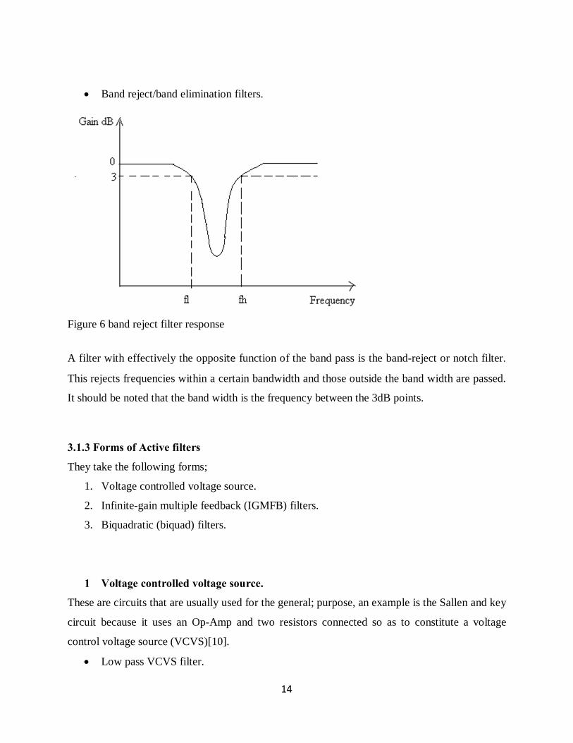
• Band reject/band elimination filters.
Figure 6 band reject filter response
A filter with effectively the opposite function of the band pass is the band-reject or notch filter.
This rejects frequencies within a certain bandwidth and those outside the band width are passed.
It should be noted that the band width is the frequency between the 3dB points.
3.1.3 Forms of Active filters
They take the following forms;
1. Voltage controlled voltage source.
2. Infinite-gain multiple feedback (IGMFB) filters.
3. Biquadratic (biquad) filters.
1 Voltage controlled voltage source.
These are circuits that are usually used for the general; purpose, an example is the Sallen and key
circuit because it uses an Op-Amp and two resistors connected so as to constitute a voltage
control voltage source (VCVS)[10].
• Low pass VCVS filter.

15
The second order transfer function is given by;
=
(3.1)
Analysis of figure 7 shows that it achieves equation 3.1 with
b O=
b1 =
(1-μ) +
+
Av = µ = 1+
(3.2)
Where µ is the VCVS and also the gain of the amplifier
Figure 7 A second order VCVS low pass filter.
• High pass VCVS filter.
The circuit is obtained from the VCVs low pass only that the positions of the resistors and
capacitors are being interchanged.
=
=
(3.3)

16
Figure 8 high pass VCVS filter
The circuit shown in the figure 8 achieves this equation with,
ao =
a1 =
(1 -μ) +
Av = µ = 1 +
(3.4)
Where µ = gain of the VCVS or the amplifiers gain.
• Band pass VCVS filter.
Higher order band pass filter may be obtained by cascading second order sections.
The second order transfer function of a band pass filter is given by the eqn…
=
(3.5)

17
Figure 9 shows as second order band pass VCVs filter.
Analysis of the circuit shows that this equation is realized when,
b = (
) (3.5.1)
wo2 = (
+
) (3.5.2)
Av = µ/R1cb (3.5.3)
Where µ = 1 +
The VCVS usually performs best when Q10 (narrow band)
Advantages of VCVS
• They have low output impedance.
• Have a low spread of values and is capable of relatively high gains.
• They have relatively eased adjustment of characteristics.
• Have a minimum number of network elements.
• Tuning can be achieved by adjusting R2 for the desired fo and then by adjusting μfor the
desired band width.

18
• Its band width can be varied by changing µ without affecting the centre frequency fo
2. The infinite multiple feed-back (IGMF) filter.
The circuit realizes the Sallen and Key networks with one less resistor. The circuit is so called
because of its feedback paths and because of the op-amps is serving as an infinite gain device
rather than an infinite gain VCVS.
a) Low pass IGMF filter.
The following circuit Figure 10 is a second order IGMF low pass filter.
Figure 10 A low-pass IGMF
The circuit achieves the following equation 3.6
=
(3.6)
With
bo =
(3.6.1)
b1 = (
+
+
) (3.6.2)
Av +
(3.6.3)
The filter has an inverting
and hence is useful if a phase shift of 180 degrees is required.

19
b) High pass IGMF filter.
A second order IGMF high pass filter is as shown in the following figure…
Figure 11 second order IGMF high pass
The transfer function,
+
(3.7)
Is achieved from the circuit with
a o =
(3.7.1)
a1 = (
) (3.7.2)
Av =
(3.7.3)
Thus this has an inverting gain.
c) Band pass IGMF filter.
Figure 12 shows a second-order IGMF pass band filter.
The circuit achieves the transfer function equation (3.8)
20
=
(3.8)
Advantages of IGMF filters
• They have low input impedance.
• They have a good stability characteristic.
• They have minimal number of networks than the VCVS pass band filter.
3. The Biquad filters
This type of filter usually requires more elements than the VCVS or IGMF filters but has
significant tuning advantage and excellent stability.
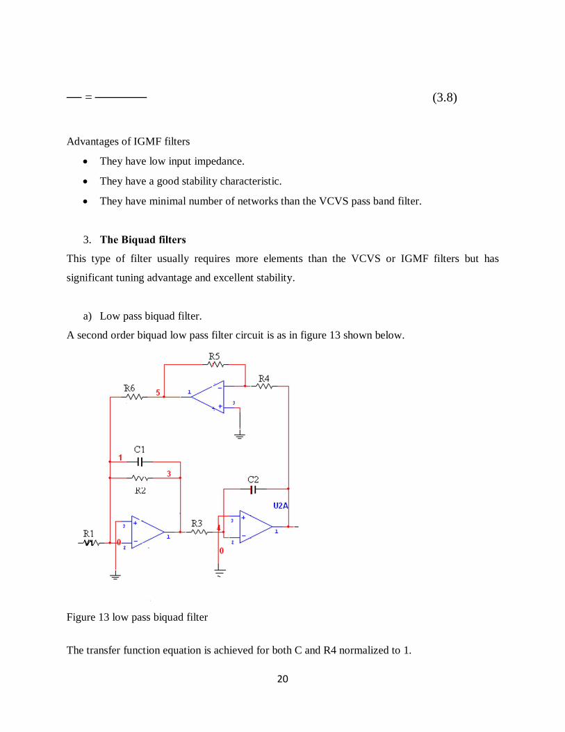
a) Low pass biquad filter.
A second order biquad low pass filter circuit is as in figure 13 shown below.
Figure 13 low pass biquad filter
The transfer function equation is achieved for both C and R4 normalized to 1.

21
Bo =
(3.8.1)
B1 =
(3.8.2)
Av =
(3.8.3)
This same results follow except that the gain is inverting if the output V o is taken at a point in
the figure 13 Op-amp A3 provides polarity reversal. Thus,
(3.9)
b. High pass biquad filters
Figure 14 High pass biquad filters The biquad circuit achieves the transfer function,
(3.10)

22
For both C and R5 normalized to 1 and an inverting gain, (Av> 0) with
A o =
(3.10.1)
A1 =
(3.10.2)
Av =
+
(3.10.3)
A second order band pass function is given by the equation 3.11 shown below,
=
(3.11)
Analysis shows that the equation 3.11 has
Av = −
(3.11.1)
B =
(3.11.2)
Wo = (3.11.3)
If an inverting gain is required, the output VO may be taken at point a
The gain is adjusted by varying R1; Q is changed by varying R2, and changing R3effect the
centre frequency.
Advantage of biquad
• It has excellent tuning features.
• It has a good stability, important in the cascading several stages.
• It is capable of attaining Q’s of 100 or more, which is beyond the capability of other
circuits.
Disadvantages
• The biquad circuits require more elements more than the other circuits.

23
CHAPTER 4
TRANSFER FUNCTIONS
4.1 FILTER TRANSFER FUNCTIONS The output and input of a linear time invariant system is related by different equations as;
= an-1 +
+ … +a1
+ aoy = bm + bm-1
+…+box (4.1)
Where x(t) is the input signal, y(t) is the output signal and n≥ mThe general form of H(s) is
H(s) = ()()
= ⋯⋯
(4.2)
Where all coefficients ai and bi are real
The function is factored into biquadratic as
H(s) = ∏ Ki =
(4.3)
Where Ki is a constant
Ai and di=1 or 0
For real zero,a1=0 bi=0
Case for real pole di=0, e1=1.
Thus for a complex pole zero pair, the biquadratic (second order filter function) can be
represented as;
H(s) = k

24
The general design procedure is the initial realization of a biquad corresponding to the filter type
then cascading of several biquads Example, the low pass and the high pass filter to obtain the
desired filter characteristics.
The biquadratic in equation …can be written as;
H(s) = K
(4.4)
Where K = Constant.
W z, W p = zero and pole of un-damped frequency respectively.
Q z, Q p = Q’s of complex zero and poles respectively.
Wp denotes the frequency at which G(s) has a peak
The 3dB bandwidth is given by:
B w =
(4.5)
The resultant frequency f r = ℎ (4.6)
And Quality factor, Q =
(4.7)
Q is the measure of the sharpness of the peak i.e. selectivity. A high Q indicates that the filter
selects a smaller band of frequencies. In most case pass band filters are made by cascading a low
pass filter circuit with a high pass.

25
The properties satisfied by transfer function, H(s) realized by active RC networks.
• H(s) is a rational function in s with real coefficients.
• All poles of H(s) must be in the left half of the s plane (for stability)
• The zeros of H(s) can be anywhere in the s plane.
• The poles of the jw axis must be in plane
• Complex poles and zeros occur in conjugate pairs.

26
CHAPTER 5
5.1 FILTER DESIGN PROCESS.
5.1.1 Filter specifications
When designing the filter the following specifications were required:
1. The cut off frequency f l, f h and f c (That is the range of pass band frequencies).
2. The allowable band pass ripple (Though some times the ripple is not permitted).
3. The band-pass frequency range.
4. The band-pass attenuation.
Another factor that is usually specified is the impedance level at both the input and output (the
interface with the signal source and load).
Often, the phase response (delay) and transient response (rise time, over-shoot) of the filter are
also specified.
Since most of the Op-Amps have a unity gain band widths, it is possible to design filters up to
frequencies of several mega hertz though at these frequencies filters are usually costly. Because
of the slew rate limitations and unit to unit variations in Op-Amp gain-band width product and
open loop gain, however, most IC active filters are used at audio frequencies.
5.1.2 The approximation phase
This is where the component values are approximated. This is derived from the transfer function H(s) =
whose associated attenuation A (w) and delay function fit within the given tolerance
boundaries.
5.1.3 The realization phase.
In-order to realize the filter, It is well done by using normalized circuits and then scaling
them to the desired values. The normalized circuit is then developed on the basis of very
simplified cut-off or centre frequency and convenient impedances level.
5.1.4 Frequency scaling
The normalized design is then converted to an actual design through frequency scaling. This
is changing the frequency of the normalized design into the required frequency of the actual
design.

27
5.1.5 Impedance scaling.
This is achieved by changing all the relative impedance levels of all components in
the filter by a specific amount to acquire a realistic and workable element values.
5.2 CLASSICAL FILTER APPROXIMATIONS It is important to note that the solution of approximation takes into consideration the
technology used, For Example, passive RLC, active RC, mechanical or crystal filters.
5.2.1 Butterworth maximally flat band pass filter functions.
The general form of the transfer function is
H (s) =
Where A(s) and B(s) are polynomial in the frequency variables. For stability the poles
of B(s) lie in the left half plane. The zeros location of A(s) are unrestricted, however
the number of finite zeros of N(s) is assumed to be equal to or less than the number of
zeros in B(s), That is the poles of H(s).
Table 5.1[10] The Biquadratic transfer function
Type of filter Form of transfer function
Low-pass
+ +
High-pass
+ +
Band-pass
+ +
Band-elimination +
+ +
Butterworth usually have a maximally flat amplitude response characteristic. The
attenuation rate of the response is approximately -20dB/decade/pole. That is
distinctively inferior to that of the Chebyshev filter.

28
5.2.2 Chebyshev ripples approximation.
This response is useful when a rapid roll of rate of more than 20dB/decade/pole is
required. Thus filters can be implemented with Chebyshev response with fewer poles
and less complex circuitry for a given roll off. This type of filter has ripples or
overshoots in the pass band and even less linear phase response. The phase response
is given by.
H (jw) =
. (5.1)
Where
= ratio of cut-off frequency of LPF
= Ratio of cut-off frequency for HPF
And k1 are constants and C n is the Chebyshev polynomial of first kind of degree n.
As n increases, the number of ripples increases and the attenuation in the band pass
increases. For K =1 is given by
F c =
or Rw = 1- √1 + (5.2)
In decibels is
R w dB = 20log√1 − ε (5.3)
5.2.3 The biquad filter
The biquad configuration is a useful circuit for producing band pass and low-pass responses,
which require high Q-factor values not achievable with the VSVS and the IGMF circuits. The
Biquad and the state variable filter circuit configuration can have Q-factor values of 400 or
greater. This circuit, whilst not as useful as the state variable, nevertheless has certain
applications. It is easily tunable using single resistor tuning (normally a stereo or ganged
potentiometer). It can be configured to produce a Butterworth or Chebychev response by
changing the damping (1/Q )[10].

29
Figure 15 Biquad filter
Figure 15 shows a typical three-operational amplifier circuit. The transfer function
is obtained by considering the band pass output first. The low-pass is easily obtained
thereafter. The Biquad active filter consists of a leaky integrator, an integrator and a
summing amplifier. Let Z f be the parallel combination of R2 and C1:
Z f =
(5.4)
The transfer function for the last stage is defined as:
=
(5.5)
In addition, for the second last stage:
=
(5.6)
The first op-amp is a leaky integrator and we can write for the output voltage as:
V2 = -
V4 -
V1 (5.7)

30
Substituting for V4 and V2 from equations 5.5 and 5.6, gives
V4 = -
V3 (5.8)
V3 = -
V2 (5.8.1)
V4 =
V2 (5.8.2)
Substituting 5.8 into 5.7 yields
V2 = -
V2 -
V1 (5.9)
V2 (1 +6 5
234) = -
1 (5.9.1)
=
(5.9.2)
=
(5.9.3)
=
(5.9.4)
If R4 = R5
=
(5.9.5)
The standard form for a band pass second order function is

31
=
(5.10)
The expressions for the pass band edge frequency, Q-factor and gain in terms of the circuit
components by comparing coefficients. The gain at the resonant frequency is
H (0) = K=
(5.10.1)
The resonant frequency becomes:
Wo2 =
(5.10.2)
Q =
(5.10.3)
B w =
(5.10.4)
The Q-factor and the resonant frequency are not independent in this circuit. For high frequencies,
the bandwidth will be the same as that for low frequencies. This, in general, is not a desirable
feature. For example, in an audio mixing desk, the equalizing section would use a state-variable
circuit where the bandwidth changes with the higher frequencies. The tuning procedure for the
Biquad BP is as follows:
1) The values for C1, C2 and R5 are selected
2) The resonant frequency ω p is adjusted by varying R3 set the gain by R1,
3) The Q-factor is set by R2. As opposed to iterative where one has to keep adjusting the
component values to get the desired value, and
4) The Q-factor is set by R2.
If C1 = C2 = C and R3 = R6 = R, are set, then the equations are greatly simplified.

32
CHAPTER 6
BAND PASS FILTER DESIGN AND EQUILIZER DESIGN
6.1 FILTER DESIGN Biquad filters have been considered due to their advantages over the types of active filter
such as multiple feedback filters, voltage controlled voltage source and crystal filter.
These advantages are;
1. Biquad has excellent tuning features.
2. It has a good stability, important in cascading several stages.
3. It is capable of attaining Q’s of 100 or more, which is beyond the capability of other
circuits.
The process of getting a band pass filter is achieved through the following three stages.
1. Designing a high pass biquad filter
2. Designing a low pass filter
3. Cascading the two filters to get a fourth order band pass. It does not depend on the one
which begins.
6.1.1 Actual problem solution
If the cut off frequency is calculated f c (Hz), filters gain G, and order n none then the
following steps are followed:
1. Select the value of capacitor c and determine the constant K parameter.
K =
(6.1)
Where the values of c are in µF
2. After that the values of resistor are obtained with assistance of table 1 below. The
resistors in the table are given for the value of k=1 and hence these values must be
multiplied with k parameter of step 1 to yield the resistance of the circuit. The

33
stage gain G and for the filter gain less than 2 the filter gain is the product of the
stage gains.
Figure 16 low pass biquad filter
Table 6.1 [1]
Chebyshev
Resistor Butterworth 0.1dB 0.5dB 1dB 2dB 3Db
R1 1.592 0.480/G 1.050/G 1.444/G 1.934/G 2.248/G
R2 1.125 0.671 1.116 1.450 1.980 2.468
R3 1.592 0.480 1.050 1444 1.934 2.248
R4 1.592 1.592 1.592 1.592 1.592 1.592
R in KΩ for a k parameter of 1 and G = 1
From the table 6.1 the standard resistor values are selected close to the ones in the table
and the filter is designed.
Q f o should be limited to much small than (Q f o = 25 KHz) to achieve Q enhancement
(Increasing the actual value of Q-effect on no ideal Op-Amp.)

34
6.1.2 Project design specifications
f h = 100Hz
f l = 40kHz
f c =
Figure 17 second order low pass filter
To obtain the component values table 6.1is used.
1st stage
DF = 2 –
(6.2)
= 2 – 1.848
R4 = 0.152R2
Let R3 = 1M
R4 = 152k
f c = √40 100 = 2KHz
B w = 40 k – 100 = 39.9 KHz
Q c = = 2
39.9 (6.3)
= 0.05Hz
fl = 100Hz =
(6.3.1)
R = 1 2100

35
Let C = 1µF
= 1.59k
For HPF
R1 R2
Let R3 =R2
DF = 2 – R4/R3
Thus
R1≅R2 ≅R3 = 1.151k
And R4 ≅ 1k
It should be noted that decreasing capacitor increases resistance.
For example
Suppose C = 1nF
R2 = 1.591MΩ
R1 = 1kΩ
6.1.3 Design procedure for a high pass biquad filter
The general circuit is as shown in the figure 6.2
Figure 18 High pass biquad filter

36
Procedure
If the cut-off were given.filter gain ,order n and filter type then
1. selecting the values of the capacitor C and determine k parameter
K =
Where C = value of C in µF
The resistance values are determined from the table 6.2.The resistance in the table is
given for the values of k = 1 and hence the value odf G must be mulfiplied by k
parameter of step 1 to yield the resistance of the circuit.The number G in the table is the
stage gain and for n> 2,The filter gain is the product of the stage gains.
The standard resistor values are chosen which are as close as posibl to those indicated in
table6.2 and construct the filter, or its stages.
Table 6.2[1]
Resistor Butter
worth
0.1Db 0.5dB 1dB 2dB 3dB
R1 1.125/G 0.671/G 1.116/G 1.450/G 1.980/G 2.468/G
R2 1.592/G 1.592/G 1.592/G 1.592/G 1.592/G 1.592/G
R3 1.125 2.223 1.693 1.598 1.630 1.747
R4 1.592 5.273 2.413 1.755 1.310 1.127
R5 1.592 1.592 1.592 1.592 1.592 1.592
Design per project requirement
C = 0.001µF, Ripple 0.1dB, let g = 4 and fc=39.9k fl = 100Hz
Thus k =
× . (6.5)
And from the table resistor values are obtained as.
R1 = 16k
R2 = 39k

37
R3 = 220k
R4 =527k
R5 = 159k
Thus the above design values of the resistors were obtained.
6.1.4 band-pass filters realization.
The band pass filter is usually realized by cascading low pass filter and high pass filter.
The manner in which they are cascaded is of no importance to the filter frequency
response. As long as the critical frequency is sufficiently separated, Thus the critical
frequency is chosen such that the response curves overlaps sufficiently. The critical
frequency of high pass must be sufficiently higher than that of low pass.
In order to allow for boost or cut, the specified frequency band an equalizer section is
cascaded with the band-pass section.
Figure 19 fourth order biquad band pass filter.

38
Realization of equalizer
The circuit is designed so that over a specified frequency band, C1 acts as an open loop
while C2 acts as a short circuit, thus, allowing for boost or cut control depending on the
wiper position is to the left or to the right. Outside the band the circuit acts as a unity gain
inverting amplifier, regardless of the wiper position. This is due to the fact that C2 acts
as a short circuit at high frequencies. The result is a flat response, but with a peak or a dip
over the specified band.
Figure 20 an equalizer circuits If the component values are selected such that
R2≫R1
R4 = 10R3
C1 = 10 C2
And the centre of the band is
fo =
And the gain magnitude Av at this frequency is variable over the range
Av

39
Typical values for each section (assuming topology of each section identical to the one shown)
R1 = 10k
R2 = 100k
R3 = 1M
The capacitance is determined using the equation 6.3.1
C1 = 19.1pF
C2 = 1.91pF
Selecting standard values for the circuit parameters close to those calculated and implemented in
the circuit.
6.2.4 Realization of band-pass as a graphic equalizer
This was realized by cascading the fourth order band pass filter with the equalizer .The output of
the band pass is the input to the equalizer circuit.
40
CHAPTER 7
FABRICATION AND TESTING THE CIRCUITS
MEASUREMENT OF THE ACTIVE FILTER This was achieved by measuring the response of each individual filter beginning with low pass,
then high pass and then the cascaded fourth order active band pass filter. Q factors and
attenuation frequencies are considered.
STABILITY It was noted that if not stable, then the output was an oscillator.
Some of the causes of instability were;
Ø An excessive capacitive load on an Op-Amp
Ø The existence of high frequency parasitic poles
Ø An Op-Amp that has too critically frequency compensated
LAB WORK AND APPARATUS Power supply
Oscilloscope
Signal generator
The circuit
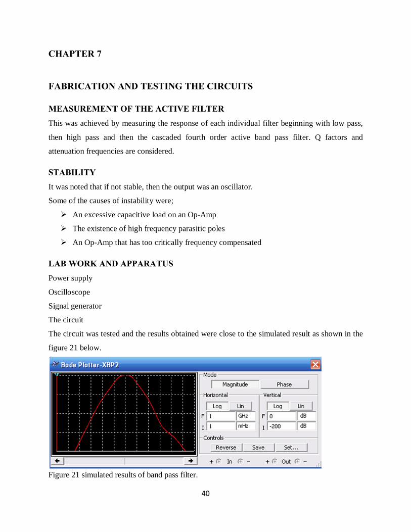
The circuit was tested and the results obtained were close to the simulated result as shown in the
figure 21 below.
Figure 21 simulated results of band pass filter.

41
CHAPTER 8
COMMENTS It was noted that the expected results were not perfectly obtained. The maximum gain at
resonance frequency is -2.8dB.
CONCLUSION The objective of the project was achieved since the values got from the test did not differ
appreciably with the simulated results. Thus the tests give a response that agrees with the theory.
The small deviations were due to:
Ø Non ideal nature of the Op-Amp
Ø The quality factor Q on capacitance was not ideal
The effects of the driving stages where the driving impedance is large rather being negligible.

42
1 Appendix Order Roll Off
dB/dec.
1st stage
Poles
DF R1/R2 2nd stage
poles
DF R1/R2
1 20 1 Optional 0.586
2 40 2 1.414 1
3 60 2 1.00 0.152 1 1.00 1
4 80 2 1.848 1 2 0.765 1.235
5 100 2 1.00 0.068 2 1.618 0.382
6 120 2 1.932 2 1.414 0.586
Table of Values of the Butterworth response[10].

43
REFERENCES [1.] Electronics Devices and circuits
Merrill publishing Division of Bell and Howell Company.1986
[2.] Filter Theory design, Active and passive
Pitman publishing company, London, 1979
[3.] Filter theory and design, Active and passive
Adels Bedraand Peter, O Blackett.
[4.] Approximation method for electronic filter design
Mc Graw-Hill book coNew York. 1979
[5.] Table of Active filter design
Geogi Publishing co.1980. St. Saparin, Switzerland 1980
[6.] Filter theory and design, Anctive and passive
Sedra, A. S and Brackett, P. O(Pitman 1979)
Van Norstrad Reinhold co. NY 1969
[7.] Active filter for Communication and instrumentation
Bownn, P and Stephenson, F .w Mc Graw-Hill 1979
[8.] Rappid practical design of Active filters
John Willey and Sons, Newyork 1975.
[9.] Electronic Filter Design Hard book.
Artur B. Willims, Fred J Taylor, 1995
[10.] Microelectronics Second Edition
Aarvin Grael
Jacob Milman, 1987

44


![Line filter Pi 1907 - pramo.lt · Line filter Pi 1907 NG 400 - 6000 4 8. Order numbers 8.1 Filter elements Nominal size NG [l/min] Order number Type Filter material max. ∆ p [bar]](https://img.dokumen.tips/doc/110x75/5b5068e97f8b9a5a6f8e686f/line-filter-pi-1907-pramolt-line-filter-pi-1907-ng-400-6000-4-8-order.jpg)


