Embed Size (px)
Citation preview

FOUR BIT SHIFT REGISTER
EE 584
GUIDED BY: SUBMITTED BY: Dr. Elias Chris Soh Adjunct Professor Karan Jhavar University of Kentucky Stephen Disney Tapan Desai (Group 13)
1

INDEX Introduction………………………………………………………………………………..2 Historical Uses…………………………………………………………………………….2 Project Description………………………………………………………………………...2 Components Used………………………………………………………………………....5 Desgin Considerations…………………………………………………………………...23Simulation………………………………………………………………………………. 26 Conclusion……………………………………………………………………………….29
2

Introduction While the goal of this class is to help students develop the necessary skills needed
to do for CMOS implementation, this project gave us an opportunity to use real industrial tools to design and build VLSI schematics and layouts. This project is primarily aimed toward designing a circuit that can be used to test the functionality, fidelity and maximum speed of shifting of a four bit SISO (Serial In Serial Out) shift register. In order to do this the inputs of the shift register are made to store and then compared with the outputs.
The speed and functionality of the shift register under test is tested at various corners, such as temperature, applied voltage and process corners. This testing is done using a simulation tool known as ‘Spectre’. Then the real world sketch of the circuit is i.e. layout, is implemented in ‘Virtuoso’ editor provided by ‘Cadence’ tool set. The layout is made to pass the DRC (Design Rule Check), and the LVS (Layout Vs Simulation) test, both, conforming to the standards of “Cypress Semiconductors Ltd.”.
Historical Uses There are a plethora of different shift register designs currently being used. Each
possessing its own advantages and disadvantages. A shift register can have a combination of serial or parallel inputs and outputs. There are also bi-directional registers that can shift both left and right. It is also possible to connect the inputs and outputs together to create a ring counter. These registers are often used to build simple delay circuits. Generally these delay circuits are used to create a serial to parallel interface. The registers can also be connected in parallel to create the hardware implementation of a stack.
SISO shift registers are generally used in multiplier circuits. Also they can be used to perform a bit to bit comparison of a data stream. However the most frequently used application of a SISO shift register is as a frequency divider. Project Description
The SISO shift register transmits data serially from one flip-flop to the next, in sequence from left to right. The shift register is designed such that at the negative edge of each clock cycle, the data present at the input is loaded into the first flip-flop, (a more detailed design is discussed below). At each subsequent negative edge of the clock, the data in the predecessor flip-flop will be loaded into the successor flip flop. This continues until the clock stops. This means the data would be shifted out from the last flip-flop and lost, unless stored. The testing circuit makes it possible to compare the outputs from each flip flop with the original inputs sent to the shift register. In order to do this testing for comparison, each of the input bits is made to store in D Flip Flops, present in the test circuitry.
It was important to store input bits in the correct order. For this, a counter and an accompanying logic had to be implemented. The counter is used to provide clocks to the input storing D-flip flops. The counter and the accompanying logic are set up such that, a perticular D flip-flop is enabled at every fourth clock cycles. This makes it possible to
3

store correct input in correct order. The order in which the input is stored is mentioned in more detail below.
The inputs storing D Flip Flops are a master and slave type flip-flops. Where slave follows master at the negative edge of the clock pulse. In the circuit involved in this project, a level high of clock is continuously applied. This makes master track input at every moment. When a particular D Flip Flop is wanted to store the input, the clock for that particular D Flip Flop is made to go low, which, makes the master stop tracking input and slave follows and stores master’s output. The logic circuit in between the counter and the input storing D Flip Flops helps in implementing this scheme. Thus, a particular D Flip Flop (i.e. slave) actually stores input at every 4th clock pulse, and, thus correct input is made to store in correct flip flop.
I/P – INPUT O/P – OUTPUT CLK – CLOCK C – COUNTER I – INVERTER N – NAND D – D FLIP FLOP E – COMPARING LOGIC S – SHIFT REG. DL – DELAY
Figure 1: Schematic of main circuit
4

Components Used NAND Gate The NAND gate is a logic device that follows the following truth table:
00 1
01 1
10 1
11 0
A schematic, symbol and layout for a two input, three input and four input NAND gates are shown below
Figure 2: Two input NAND gate
5

Fig 3: Symbol view of two input NAND Gate
Fig 4: Layout of tow input NAND gate
6

Figure 5: Three input NAND
Fig 6: Symbol view of three input NAND gate
7

Fig 7: Layout of three input NAND gate
8

Fig 8: Schematic of 4 input NAND gate
Fig 9: Symbol view of 4 input NAND gate
9

Fig 10: Symbol view of a 4 input NAND gate
10

Transmission Gate A transmission gate is basically made up of a PMOS and NMOS transistor. Looking at Fig 12 below, clk1 is the opposite of clk2. That is if clk1 is one clk2 is zero. When clk2 is high then in1 is passed out 1. If the clk1 and clk2 are different than mentioned above, the output of transmission gate is ‘Z’ (High Impedance State). It is basically used for separating two circuits or used as an enabling logic. The disadvantage of using a transmission gate is that it takes up more area in the layout. However the fact that the transmission gate gives a rail to rail swing from 0 to 1 means the layout problems can be overlooked.
Fig 11: Schematic transmission gate
11

Fig 12: Symbol view of transmission gate
Fig 13: Layout of transmission gate
12

Counter
A counter counts in a predefined sequence. When given a clock as an input, the counter changes its state (i.e. counts), at every clock pulse. The normal (2 bit) BCD counter counts in the given sequence: (assuming that the initial state of bit’1’ and bit’2’ before application of clock is ‘0’)
After application of:
BIT 1 BIT 2
1st Clock 0 1 2nd Clock 1 0 3rd Clock 1 1 4th Clock 0 0
The counter was designed using TK Flip Flops and digital designing fundamentals involving ‘State Table’ and ‘Excitation Table’.
Fig 14: Counter schematic
13

Fig 15: Simulation of counter
Fig 16: Symbol view of counter
14

Negative Edge-Triggered D flip-flop A negative edge triggered flip-flop changes state at the negative edge of the clock.
This means that when the clock goes from 1 to 0 a new input is stored and the old input gets passed. The D flip-flops used in the shift register are a master slave combination. When clock goes high the input is tracked by the master. When the clock goes low the input is captured by the slave through the master.
Looking at Fig 17 when clock is high, T1 and T4 are turned on. T2 and T3 are turned off. The input is tracked by the master. When the clock goes low T2 and T3 turn on. T1 and T4 turn off. This means the value in the master is passed to the slave thus passed to the output. Set gives the flip-flops an initial state either one or zero. Reset when triggered, would set the flip-flop to its initial state.
Fig 17: Schematic of D-flip flop
15

Fig 18: Symbol view of D flip-flop
Fig 19: Layout of D flip-flop
16

The center of the D flip flop is composed of the transmissions gates. They are group together so that they make a densely packed center. Since the outputs never leave the D flip-flop the NAND gates are positioned around the transmission gate. This means the signals have the shortest path to any internal piece of the D flip-flop. This was done in the hopes that the final D flip-flop would be as densely packed as possible. This will reduce the overall area for circuitry. Shift Register The four but shift register is simply 4 negative edge-triggered master slave D-flip flops connected in series. It operates in a similar fashion to the negative edge triggered D-flip flops. When the clock transitions from high to low the input is loaded into the first shift register. On every subsequent clock pulse the input is shifted from one flip flop to the next serially. This process will shift the original input from left to right.
Fig 20: Schematic of shift register
Fig 21: Symbol view of the shift register
17

Fig 22: Simulation of shift register performance
18

Description of D- Flip Flop in test circuit The D-flip flops in the test circuit operate exactly as the ones in the shift register. The only difference between the two is the channel lengths of the transistors. The transistors in these flip flops have a channel length of 0.5 micrometers.
Fig 23: Schematic of D-flip flop
Fig 24: Symbol view of D flip-flop
19

Fig 25: Layout of D flip-flop The center of the D flip flop is composed of the transmissions gates. They are group together so that they make a densely packed center. Since the outputs never leave the D flip-flop the NAND gates are positioned around the transmission gate. This means the signals have the shortest path to any internal piece of the D flip-flop. This was done in the hopes that the final D flip-flop would be as densely packed as possible. This will reduce the overall area for circuitry.
20
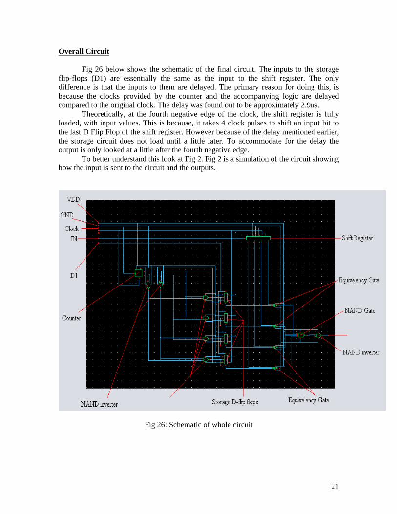
Overall Circuit
Fig 26 below shows the schematic of the final circuit. The inputs to the storage flip-flops (D1) are essentially the same as the input to the shift register. The only difference is that the inputs to them are delayed. The primary reason for doing this, is because the clocks provided by the counter and the accompanying logic are delayed compared to the original clock. The delay was found out to be approximately 2.9ns.
Theoretically, at the fourth negative edge of the clock, the shift register is fully loaded, with input values. This is because, it takes 4 clock pulses to shift an input bit to the last D Flip Flop of the shift register. However because of the delay mentioned earlier, the storage circuit does not load until a little later. To accommodate for the delay the output is only looked at a little after the fourth negative edge. To better understand this look at Fig 2. Fig 2 is a simulation of the circuit showing how the input is sent to the circuit and the outputs.
Fig 26: Schematic of whole circuit
21

Fig 27: Simulation of the circuit
22

Design Considerations Counter
When running the simulations for the counter a design error occurred. After the application of the 2nd clock pulse in the 2 bit BCD counter, it was seen that both ‘b2’ and ‘b4’ (refer to simulation of counter) changed state at the same time. This was undesirable as the purpose of the logic was to make only ‘b2’ go low. This will enable only one input storing D Flip Flop to, actually store the input. If both ‘b2’ and ‘b4’ go low at the same time, their respective input storing D Flip Flop are enabled. If this happens, both D Flip Flops will store the input and the comparing logic of the circuit ‘may’ give a wrong indication of matching (or faithfulness of the shift register). Essentially this should happen after 4th clock pulse (i.e. indication of faithfulness of shift register). However if the original counter was used, the comparing logic showed the faithfulness of the shift register before the 4th clock pulse. The problem arouse because ’BIT 1’ and ‘BIT 2’ were transitioning at the same time, at the application of the 2nd clock pulse. Since the transition is not ideal the circuit wrongly interpreted a change of state of ‘BIT 1’ from ‘0’ to ‘0’ and ‘BIT 2’ from ‘1’ to ‘0’. Instead of ‘BIT 1’ from ‘0’ to ‘1’ and ‘BIT 2’ from ‘1’ to ‘0’. This enabled the input storing D Flip Flop, which responded (or stored) at the application of the 4th clock pulse.
By designing the counter in the above format, i.e. counting sequence, where, only one bit changed state at a time. This eliminated the problem of both ‘b2’ and ‘b4’ go low at same time.
actual transition wrongly interpreted transition
The counter involved in this project is designed as such to count in the given sequence:
BIT 1 BIT 2
1st Clock 0 1 2nd Clock 1 1 3rd Clock 1 0 4th Clock 0 0
23

Designing of the counter was done using TK Flip Flops and digital designing fundamentals involving ‘State Table’ and ‘Excitation Table’. Shift Register
From the simulations we found that the shift register always breaks at a lower frequency, than the counter, for same set of conditions. If the counter breaks before the shift register then our simulations will not give the correct data. The frequency of the clock was increased until the breaking point of the shift register was found. Then the simulations were used to find were the counter breaks, were also performed. The simulations showed the counter was breaking before the shift register. This the because, the D Flip Flop breaks at a higher frequency as compared to the counter (JK Flip Flop), for same W/L (Width over Length) ratio. The easiest solution was changing the channel lengths of the MOSFETS used in the shift register. The channel lengths were changed from 0.5 micrometers to 0.6 micrometers. This ensured, that the shift register loses fidelity at lower frequency, than at which a counter does, at same set of input conditions.
Figure 28 below shows the point at which the shift register breaks. The clock frequency at which the shift register breaks is 0.22 GHz. Using this clock frequency the counter was simulated. Figure 29 below shows the simulation of the counter. It can be seen that the counter works at this frequency. Therefore the shift register breaks before the counter.
24

Fig 28: Simulation of shift register breaking
Figure 29: Counter working at breaking frequency of shift register
Synchronization
It was also noticed that a significant delay existed through the counter and accompanying circuit. This caused a synchronization problem. The problem was between synchronization of inputs to clock pulse at the storage D Flip Flops. This caused output to be wrong. A method to slow the clock going to the counter had to be considered.
An integrator can slow the clock down. However using an integrator means the capacitance value has to be calculated for each frequency simulation. Thus, in order to concentrate more on project objectives and applicable, timing constraints, it was assumed that there is availability of a delayed version of the inputs, given to the circuitry. Simulations
25

Simulations to find the effect of VDD and frequency, frequency and temperature
and VDD and temperature were performed. These simulations are done under the typical, fast and slow conditions. From the simulations the behavior of the shift register under conditions mentioned above can be observed. Typical Simulations As mentioned earlier the input to the storage flip-flops has to be delayed longer then the input. This can be seen in the plot below. D1 is delayed 3 ns longer then ‘in’(input data).
Fig 30: Simulation of final circuit
26

Using the same set up for D1, in, reset and clk as above the various effects of temperature frequency and VDD was simulated. VDD and Frequency For each test shown below the temperature was fixed at 27oC. Then as shown above, the simulation was set up and the simulation was run. A 1 represents the circuit working. A zero represents the circuit failing. At each frequency the VDD was swept from 1.6V to 2V in steps of 0.5V. Vdd 0.2 G Hz 0.22 G Hz .23 GHz .24G Hz .25G Hz .26 G Hz 2.0 1 1 1 1 1 1 1.95 1 1 1 1 1 1 1.9 1 1 1 1 1 1 1.85 1 1 1 1 1 1 1.8 1 1 1 0 0 0 1.75 0 0 0 0 0 0 1.7 0 0 0 0 0 0 1.65 0 0 0 0 0 0 1.6 0 0 0 0 0 0 Temperature and Frequency For each test shown below the VDD was fixed at 1.8V. Then as shown above, the simulation was set up and the simulation was run. A 1 represents the circuit working. A zero represents the circuit failing. At each frequency the temperature was swept from ------155oC to 155oC in steps of about 30oC. Temp 0.2 G Hz 0.22 G Hz .23 GHz .24G Hz .25G Hz .26 G Hz 155 1 1 1 1 1 1 100 1 1 1 1 1 1 55 1 1 1 1 1 1 27 1 1 1 0 0 0 0 0 0 0 0 0 0 -30 0 0 0 0 0 0 -155 0 0 0 0 0 0
27

Temperature and VDD For each test shown below the frequency was fixed at 0.2 GHz. Then as shown above, the simulation was set up and the simulation was run. A 1 represents the circuit working. A zero represents the circuit failing. At each temperature the VDD was swept from 1.6V to 2V in steps of 0.5V Vdd -155 -30 0 27 55 100 155 2.0 0 0 0 1 1 1 1 1.95 0 0 0 1 1 1 1 1.9 0 0 0 1 1 1 1 1.85 0 0 0 1 1 1 1 1.8 0 0 0 1 1 1 1 1.75 0 0 0 0 1 1 1 1.7 0 0 0 0 1 1 1 1.65 0 0 0 0 1 1 1 1.6 0 0 0 0 1 1 1
28

Conclusion
The shift register was simulated with the test circuitry. Using the test circuitry, the functionality of the shift register can be observed. The simulations were performed under different corners and the information was recorded. Using this data an operating range for the frequency divider can be found.
All the inputs and outputs of the circuitry were connected to the pads in the bounding the box. This means that using oscilloscope probes the inputs and outputs can be observed to find were the test circuitry breaks.
29


![74HC164; 74HCT164 8-bit serial-in, parallel-out shift register · 8-bit serial-in, parallel-out shift register [1] The input and output voltage ratings may be exceeded if the input](https://img.dokumen.tips/doc/110x75/5ce599c888c993b62d8bbe66/74hc164-74hct164-8-bit-serial-in-parallel-out-shift-register-8-bit-serial-in.jpg)
![74HC165; 74HCT165 8-bit parallel-in/serial out shift register · 2016-01-12 · 8-bit parallel-in/serial out shift register [1] The input and output voltage ratings may be exceeded](https://img.dokumen.tips/doc/110x75/5e921a9249b0587de52357d2/74hc165-74hct165-8-bit-parallel-inserial-out-shift-2016-01-12-8-bit-parallel-inserial.jpg)


