Embed Size (px)
Citation preview

Formation of ZnO in or on glasses by using the Sol-Gel and Chemical
Bath Deposition Techniques
S. J. CASTILLO1, M. C. ACOSTA-ENRÍQUEZ1, MA. E. ZAYAS1, H. ARIZPE1, T. MENDÍVIL-REYNOSO1, A. GARCIA-JUÁREZ1, M. E. ALVAREZ-RAMOS2 AND E. LARIOS-
RODRÍGUEZ3,4 1Departamento de Investigación en Física, Universidad de Sonora, Apdo. Postal 5-088, CP. 83000,
Hermosillo, Sonora, México. 2Departamento de Física, Universidad de Sonora, Apdo. Postal 1626, CP. 83000, Hermosillo, Sonora,
México. 3Departamento de Investigación en Polímeros y Materiales, Universidad de Sonora, CP. 83000,
Hermosillo, Sonora, México. 4Departamento de Ingeniería Química de la Universidad de Sonora, CP. 83000, Hermosillo, Sonora,
México.
[email protected] http://www.cifus.uson.mx Abstract: - In the first part of this work was produced Zinc Oxide (ZnO) into a glass matrix by using the Sol-Gel Technique at room temperature, these materials were prepared using tetraethyl orthosilicate (TEOS) as precursor, the Zn ions were added before the jellification step trough an aqueous solution of zinc acetate. These glasses were characterized by X-ray diffraction, optic absorption, FT-IR and Raman spectroscopy. The X-ray patterns showed amorphousness. The optical absorption shows a shoulder in the UV range corresponding whit ZnO confined to the vitreous matrix. The spectra by FT-IR show characteristic vibrations of Si-O-Si with interaction Zn+2. Raman scattering let us to identify and precise the formation of the ZnO. In the second part of this work was immersed glass substrates into an aqueous chemical bath with external controlled temperature, the chemical solutions contained in the bath were a Zn Ions source (ZnSO4) 0.1 M, a pH 10 Buffer solution (NH4Cl/NH4OH), Ethanolamine to complex the Zn ions, and pure water, resulting ZnO films hexagonally structured with energy band gap of 3.3 eV, growing 1000 nm during 25 minutes followed of 60 minutes to 75°C and 85°C in the same chemical reaction.
Key-words: Glasses, Zn Ions, Zinc Oxide, Sol-Gel Process, Thin Films, Chemical Bath Deposition and semiconductors
1 Introduction Zinc oxide has attracted a significant attention in
the last decades because its wide band gap behavior which confers a host of potential applications in gas sensors [1], solar cells [2, 3], Catalysis [4], Organic light emitting diodes (OLEDs) [5], microelectronic devices how transistors [5-9], particularly a very interesting use of the ZnO is like electronic devices with highly nonlinear current-voltage relationships called Varistors [10-14]. At small applied electric fields, varistors are insulating; but at a fairly well-defined higher field, those switch to conducting and maintain a nearly constant field over many decades or magnitude orders of current. Most commercial, and military application varistors are based on polycrystalline, semiconducting ZnO with a variety of other oxide additives typically in the molar range of 100 parts per million to several percent. Their
main application is in electrical circuits to limit or regulate the voltage that can be applied to other devices or components. While it is common for varistors to operate with current densities of 10-3 to 10 A/cm2, some others applications also require unusually high electric fields near 40kV/cm. With these high power conditions, it is perhaps not surprising those small flaws in the varistor result in breakdown, or a large irreversible change in their electrical and sometimes structural properties. The functional dependence of current on voltage in these devices is symmetrically bipolar that is due to an inherent property of the semiconductor from which it is made.
Several process using both chemical and physical methods have been reported for the production of these materials (ZnO and ZnO-composites) like tape casting[14], sol-gel[15-16], vapor-phase transport
WSEAS TRANSACTIONS on CIRCUITS and SYSTEMS
S. J. Castillo, M. C. Acosta-Enriquez, Ma. E. Zayas, H. Arizpe, T. Mendivil-Reynoso, A. Garcia-Juarez, M. E. Alvarez-Ramos, E. Larios-Rodriguez
ISSN: 1109-2734 143 Issue 3, Volume 9, March 2010
method[17], chemical vapour transport (CVT) process, spray pyrolysis (SP)[18], sputtering, etc., either to produce powders, thin films, nanoparticles, nanorods, composites, etc. Particularly ZnO-composites either using a matrix of glass, ceramic or polymeric, are very attractive since these composites offer many possibilities for creating new materials, especially for microelectronics and nanoelectronics industry, because through appropriate techniques can be homogeneously disperse the particles of the semiconductor (ZnO) in the matrix chosen. Furthermore, ZnO thin-film transistors (TFT) have recently received much attention due to their potentials toward a new driving component for liquid crystal display and other applications like solar cells, etc.
The purpose of this work is to study two alternative ways to prepare composites containing SiO2 glasses and Zn ions or ZnO molecules. The first one, by using the sol-gel technique, is a way to prepare this kind of the required composites starting from TEOS as precursor, then the Zn ions are added trough an aqueous solution of Zn(CH3COO)2•2H2O in the process, before the gel formation. The process is carry on at room temperature and the complete process is as simple as the sol-gel technique. The second one, by Chemical Bath Deposition (CBD) technique using two reaction temperatures T1 =75°C and T2 = 85°C, during respective times of 25 minutes and 1 hour, in the same reaction.
2 Materials and Methods The used chemicals compounds were reagent
grade, but with purities between 98 to 99%. For the first composites were used Deionized Water, Absolute Ethanol, Tetraethyl Orthosilicate, Chlorhydric Acid and Zinc Acetate. For the second composites kind were used Deionized Water, Zinc Sulfate, Buffer Solution pH 10 (NH4OH/NH4Cl), Ethanolamine and Corning brand microscope slides as substrates. 2.1 Experimental Method to produce ZnO
into a glass matrix by using the Sol-Gel
Technique Ten samples with different proportions of zinc
ions were prepared, where the ZnO single molecules or nanoparticles were formed being embedded into the SiO2 phase. The starting solutions were prepared by mixing TEOS, water and ethanol. This set of samples was prepared using a constant ethanol:TEOS volume ratio of 1:1 and a volume ratio of water : TEOS, 1:1. The solution was catalyzed with 50 drops of concentred HCl (or some
dilution), in order to homogenize its phases, Sol formation. It is necessary to wait several days (7-15) to dry the monoliths. After jellification all samples were dried and/or ground to obtain a fine powder at room temperature. The zinc was incorporated into the samples, dissolving Zn (CH3-COO)2 into water and added to the starting solution. The amount of the zinc acetate varied from 0.1 M to 1.0 M, see Table 1.
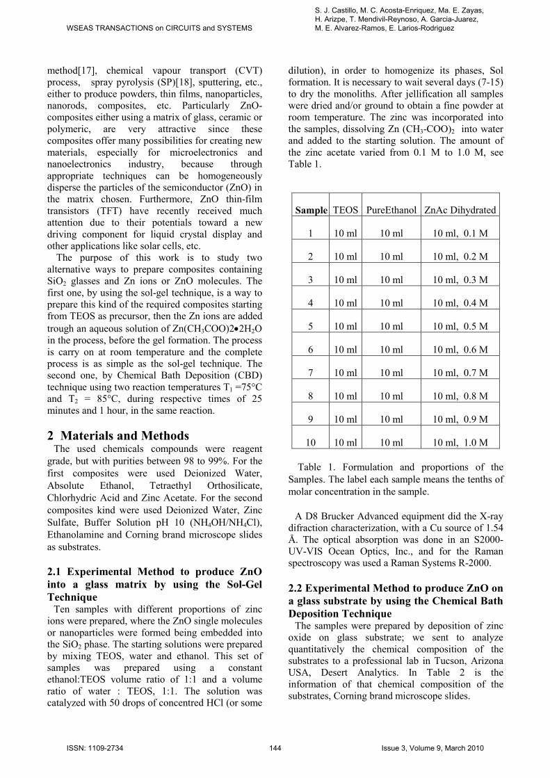
Sample TEOS PureEthanol ZnAc Dihydrated
1 10 ml 10 ml 10 ml, 0.1 M
2 10 ml 10 ml 10 ml, 0.2 M
3 10 ml 10 ml 10 ml, 0.3 M
4 10 ml 10 ml 10 ml, 0.4 M
5 10 ml 10 ml 10 ml, 0.5 M
6 10 ml 10 ml 10 ml, 0.6 M
7 10 ml 10 ml 10 ml, 0.7 M
8 10 ml 10 ml 10 ml, 0.8 M
9 10 ml 10 ml 10 ml, 0.9 M
10 10 ml 10 ml 10 ml, 1.0 M Table 1. Formulation and proportions of the
Samples. The label each sample means the tenths of molar concentration in the sample.
A D8 Brucker Advanced equipment did the X-ray
difraction characterization, with a Cu source of 1.54 Å. The optical absorption was done in an S2000-UV-VIS Ocean Optics, Inc., and for the Raman spectroscopy was used a Raman Systems R-2000.
2.2 Experimental Method to produce ZnO on
a glass substrate by using the Chemical Bath
Deposition Technique The samples were prepared by deposition of zinc
oxide on glass substrate; we sent to analyze quantitatively the chemical composition of the substrates to a professional lab in Tucson, Arizona USA, Desert Analytics. In Table 2 is the information of that chemical composition of the substrates, Corning brand microscope slides.
WSEAS TRANSACTIONS on CIRCUITS and SYSTEMS
S. J. Castillo, M. C. Acosta-Enriquez, Ma. E. Zayas, H. Arizpe, T. Mendivil-Reynoso, A. Garcia-Juarez, M. E. Alvarez-Ramos, E. Larios-Rodriguez
ISSN: 1109-2734 144 Issue 3, Volume 9, March 2010

Element Concentration Compound Concentration
Al 0.702 Al2O3 1.326 Si 34.039 SiO2 72.82 Na 8.527 Na2O 11.494 Mg 2.478 MgO 4.108 S 0.107 SO2 0.214 P 0 P2O5 0 K 0.696 K2O 0.839 Ca 4.702 CaO 6.578 Fe 0 FeO 0 Mn 0 MnO 0 Ti 0.003 TiO2 0.005 O 46.131 Stoichiometry -
Total 97.385 total 97.384
Table 2. Quantitative analysis and chemical
composition of the Substrates sent to analyze to a professional lab in Tucson, Arizona USA, Desert Analytics.
Whereas, in Table 3 we tabulate the technical
information of the provider of substrates.
Composition Percent approx.
SiO2 73%
Na2O 14%
CaO 7%
MgO 4%
Al2O3 2%
Table 3 Technical information published for the
provider of substrates.
The chemical bath deposition (CBD) is used for deposition techniques that produce a solid film in a single immersion through control of the kinetics of formation of the solid. Film thickness and composition can be easily controlled by changing simple reaction parameters such as reactant concentration, reaction temperature and deposition time. The deposition medium for CBD consists of one or more salts of metal Mn+, a source for a chalcogenide (if the film to be deposited contains S, Se, etc), a source of oxygen for oxide films and a complexing agent (e.g. ammonia, NH3, EDTA, sodium citrate, etc.) all mixed in aqueous solution.
For oxides, water normally provides the oxygen. The processes that occur in the CBD solution consist in general of the following five steps: (1) Time zero to equilibrium between the complexing agent and water; (2) Hydrolysis of the chalcogenide source (if the film is not an oxide); (3) Formation and/or dissociation of ionic metal–ligand complexes [M(L)i]
n-ik, where Lk- denotes one of more ligands, and (4), (5) Formation of the solids. Step (4) consists of the oxidation of a metal hydroxide from the water release. Step (5) the controlled reaction of metallic cations either with ionic oxygen or chalcogenides ions by mean of release complexing agents.
Now schematically, CBD for oxide or sulfide films from a metal cation Mn+ complexed by i ligands Lk-, can be depicted as follows (five steps):
1) Dissociation of water and Complexant-water
equilibrium:
−++→← nOHnHOnH 2
−+−−+→←+ OHHLOHL k
i
k
i 2)(22)(2 12
2) Thiourea hydrolyzes to form sulfides
OnHNnCHnS
nOHNHnSC
2222
22
2
2)(
++
→+
−
−
3) Displacement of ligands:
−+−−+→+
k
in
ikn
i LsOHMLMnOH )()()()( )(
4) Deprotonation to form oxides
OHn
sMOsOHM nn 22 2)()()( +→
5) Total Reactions:
−++
−++→+
k
in
ikn
i LnHsMOOHn
LM )()(2
)( 22)(
−−+
−+→+
k
in
ikn
i LsMSnSLM )()()( 22)(
WSEAS TRANSACTIONS on CIRCUITS and SYSTEMS
S. J. Castillo, M. C. Acosta-Enriquez, Ma. E. Zayas, H. Arizpe, T. Mendivil-Reynoso, A. Garcia-Juarez, M. E. Alvarez-Ramos, E. Larios-Rodriguez
ISSN: 1109-2734 145 Issue 3, Volume 9, March 2010

The complexant is optional and is usually chosen
based on the affinity of its ligands toward the metal. This makes step 3 the rate-determining step, adding a degree of control for thin film thickness. The hydrolytic process of reactions 4 and 5 can be accelerated by heating the solution, which induces deprotonation of the hydrated metal species (reaction (4)). This eliminates the need to use a base in reactions 4 and 5. For the oxide systems to be formed in this research work, hydrolysis can occur even in acidic solutions when the metal cation is easily hydrolysable, as in the case of some of the metals to be evaluated here (Al3+, Zn2+, In3+). In contrast, CBD of non-oxides requires the addition of basic solutions. In all CBD processes, whether oxide or non-oxide, a solvated metal complex reacts with a chalcogenide source to form a desired solid product. The main difference is that for oxides, the ‘‘chalcogenide source’’ is water, so that tighter control must be exerted over just two parameters (pH, T) to achieve a similar degree of control over the rate of hydrolysis and, therefore, control over the film’s microstructure and properties. For non-oxide films, the supply of chalcogenide anions can be controlled, in addition to pH and temperature, with the concentration of the chalcogenide source.
The practical procedure is too simple, consists to immerse the substrate into the solution (bath) containing an aqueous solution of complexed zinc sulfate, until the zinc oxide thin film is formed on the glass substrate.
Reagents used to deposit of ZnO thin films in a two-stage temperatures process; 25 minutes at 75°C and 1 hour at 85°C, in the same reaction bath: • 36 ml of zinc sulphate (ZnSO4) 0.1 M. Source
metal. • 12 ml of pH 10 controller buffer
(NH4Cl/NH4OH). • 18 ml of Diluted Ethanolamine in deionized
water, 50%:50%. Complexing agent. • Complete to a volume of 100 ml with deionized
water. This process has a singular complication as
reaction condition which is: If we start to a initial temperature like the ambient, ~ 21 °C, it is necessary to consider a first reaction with small temperature gradient, until arrive to 75 °C, 25 minutes remaining in the latter, subsequently increasing the temperature to reach 85 °C for 1 hour.
Some equipment used to analyze this second kind of composite were: X-ray diffraction was done in a Philips X'Pert; studies of optical absorption UV -Vis
was carried out using a UV-Vis spectrophotometer brand Perkin Elmer, Model 330; the image of the surface morphology, was performed with a scanning electron microscope brand Topcon SM-510 (SEM); the Raman spectra were obtained with the equipment Micro-Raman scattering brand LABRAM-Dilor. The thickness was done directly and enough accurate by using a profilometer brand Dekatar.
3 Results Developed materials are of two types, so the
presented results in this section will try to maintain a systematic independence
The monoliths of silicon dioxide with embedded zinc oxide particles are amorphous, they scatter the light and even some of them are opaque. The monoliths ere characterized by X-ray diffraction, UV-Visible and Raman spectroscopies, which below are explained in some detail. Similarly the growth Zinc Oxide Thin films on glass substrates led to a polycrystalline hexagonal structure, 1µm thickness and they were more completely characterized by X-ray diffraction, visible, Auger and Raman spectroscopies, and additionally its morphology was studied by scanning electron microscopy.
3.1 ZnO-Glass matrix composites by Sol-Gel
Technique (SiO2: ZnO) Let us to begin with the commentary that the
composites obtained had a drying time between 7 to 15 days. Also it is necessary to know that when added low proportions of zinc acetate, the composites were of a more translucent appearance, whereas that the obtained composites using the higher concentrations had opaque appearance.
We could have to measured more features for this material, but it is necessary to break the research in order to report some partial results if not this
The XRD patterns obtained showed that all the samples were amorphous compounds, as can be observed from Fig. 1. The behavior it is very similar between each gel, basically amorphous. However we can see that the wide band between 2θ = 17-35° is better defined with increase of content acetate of zinc. A little peak appears at 2θ=34°, samples corresponding to 0.8 and 0.9 M, which can correspond to hexagonal ZnO structure. Here we can consider that the sensitivity of the XRD indicates the ZnO- Glass matrix composites have
WSEAS TRANSACTIONS on CIRCUITS and SYSTEMS
S. J. Castillo, M. C. Acosta-Enriquez, Ma. E. Zayas, H. Arizpe, T. Mendivil-Reynoso, A. Garcia-Juarez, M. E. Alvarez-Ramos, E. Larios-Rodriguez
ISSN: 1109-2734 146 Issue 3, Volume 9, March 2010

not crystalline particles (SiO2: ZnO).
5 10 15 20 25 30 35 40 45 50 55 60 65
0
50
100
150
200
250
300
350 GlassesContaining ZnO
ZnAc1.0M
ZnAc0.9M
ZnAc0.8M
ZnAc0.7M
ZnAc0.6M
ZnAc0.5M
ZnAc0.4M
ZnAc0.3M
ZnAc0.2M
ZnAc0.1M
Inte
nsit
y (A
.U.)
2θ (Degrees)
Fig1. XRD patterns of glasses with zinc ions
(ZnO), showing essentially the amorphousness of the samples.
Zinc oxide has a wide direct band gap of slightly
bigger than 3 eV (~ 400 nm). It is a great UV absorber. The Fig. 2 shows the absorption spectra with different contents of acetate of zinc. We can see an increasing of the optical absorption rising from 300 nm toward UV region in the graph. This plot also shows an absorption edge located at about 420 nm, (the inflection point), which means that ZnO is present in amorphous form in the samples.
They showed opaqueness lead to a diffuse detection of the intensity by the UV-Vis spectroscopy technique, but any way the main behave follows the same features of the involved material, we should not forget that this ZnO formation it is of very small and scattered particles. This also corresponds with the global amorphousness.
250 275 300 325 350 375 400 425 450
0.00
0.02
0.04
0.06
0.08
0.10
0.12
0.14
7
810
3
46
5
192
Glasses
containing
ZnO
Optical absorption (A. U.)
Wavel engh t (nm)
Fig. 2 Absorption spectra of glasses with zinc ions (ZnO), in the 245-500 nm range. All the samples, except the number 7 show typical ZnO behavior.
In Fig. 3 are shown the absorption spectra in the 425-640nm range, these spectra have a similar behavior for almost all samples. In fact absorption edges are weak in the zone of the 400-500 nm; from there the spectra behavior remains almost constant. The low intensities surely correspond with the opaqueness and to the dispersive of most of the samples.
Fig. 3 Absorption spectra of glasses with zinc ions
(ZnO), in the 425-640 nm range. Curiously, the labeled samples 1 and 2 begin an absorption edge
450 500 550 600
-0.05
0.00
0.05
0.10
0.15
Glas ses
containing
ZnO
Th e use d mo lar co ncen tration of
O i n th e sam ple
i t is co rresp on din g to th e la bel
10
9
8
7
65
4
3
2
1
Optical absorption (A. U.)
W avelenght (nm )
WSEAS TRANSACTIONS on CIRCUITS and SYSTEMS
S. J. Castillo, M. C. Acosta-Enriquez, Ma. E. Zayas, H. Arizpe, T. Mendivil-Reynoso, A. Garcia-Juarez, M. E. Alvarez-Ramos, E. Larios-Rodriguez
ISSN: 1109-2734 147 Issue 3, Volume 9, March 2010

around 500 nm.
In the Figure 4 is shown the IR spectrum of eight of the ten studied samples. In order to understand the origin of the above glass structure in this spectrum is observed an intensive peak at 1100 cm-1, which can be attributed to characteristic vibration of Si-O-Si bridges in the silica network [19-21]. The band seen at 965cm-1, can be related to the Si-O-H stretching vibration [21-22], this peak increases as the concentration of Zn decreases, which is expected since the signal of the silicon bonded to hydroxyl groups would be more intense.
The band at around 800 cm-1 observed for all the considered concentrations, vary likely due to interaction between Zn+2 and the silica glass network which can result between the two characteristic bands for silica at 800cm-1 and 470 cm-1.
4000 3750 3500 3250 3000 2750 2500 2250 2000 1750 1500 1250 1000 750 500
0
10
20
30
40
50
60
70
80 GlassesContaining ZnO
Decreasing
Order Plots:
0.2 M
0.4 M
0.3 M
0.5 M
0.8 M
0.6 M
0.9 M
0.7 M
Intensity (A.U.)
Frecuency (cm-1)
Fig. 4 Infrarred spectrum of our glasses with zinc ions (ZnO).
From the Raman spectroscopy patterns can be
identified a signal corresponding to ZnO, see Figure 5, there are shown Raman spectra of as grown samples at room temperature; with different molar concentration. Two broad bands are shown, corresponding to ZnO (435 cm-1) and SiO2, as we already appointed. As it can be seen, small molar concentrations result in larger peak intensities. The peak at 435 cm-1 is related with E2 mode for ZnO.
It is possible to use Raman Spectroscopy excited by laser light of various wavelengths to study LO and TO modes in polar and nonpolar semiconducting materials, the frequency variations of the LO and TO modes in polarized semiconducting material like
ZnO Nano-Particles (NPs) have distinct physical origins to first order so we can do such an analysis from the experimental Raman spectra of ZnO Bulk-powder (BP) and NPs, excited by 514.5nm laser line, respectively. The first order Raman modes A1T, E1T, E2 (H), A1L and E1L are identified as the peaks at: 385, 426, 437, 572 and 584 c m−1
On other hand, Zinc acetate in pure form shows a large peak in its Raman Spectra, located at 960 cm-1, as it can be see Fig. 5. This peak is related with CH-out of plane molecular stretching bond [24]. In our samples, this peak could disappear with a thermal annealing, due to breakage of the organic bonds by heating.
Samples in pure powder at RT show two Raman small signals at 435 cm-1 and 556 cm-1 corresponding to reported in other works [23]. Both peaks have a small intensity varying for different concentrations. The peaks at both positions are related with oxygen vacancies in ZnO [20].
ZnO can be derived in Sol-Gel procedures starting with TEOS. In this case, Raman spectra will show a broad band raising from 500 to 550 cm-1 corresponding to SiO2. This band can overlap the second mentioned Raman signal for ZnO.
300 400 500 600 700 800 900 1000
0
250
500
750
1000
1250
924702419
GlassesContaining ZnO
8
6
2
4
5
3
1
7
9
10
Intensity (A. U.)
Raman shift (cm-1)
514
Fig. 5. Raman spectra of our glasses with zinc ions (ZnO).
WSEAS TRANSACTIONS on CIRCUITS and SYSTEMS
S. J. Castillo, M. C. Acosta-Enriquez, Ma. E. Zayas, H. Arizpe, T. Mendivil-Reynoso, A. Garcia-Juarez, M. E. Alvarez-Ramos, E. Larios-Rodriguez
ISSN: 1109-2734 148 Issue 3, Volume 9, March 2010

3.2 ZnO Thin Films on Glass substrate
composites by CBD technique (ZnO/Glass) Here we describe the specific characterization
developed to study our second material, this material is inorganic semiconductor type metal-chalcogenide and it is obtained in the form of thin films by the method of chemical bath deposition. Thanks to the versatility of this method or technique, it would be possible to vary a number of physical and chemical parameters that allow us to modify the properties of the obtained semiconductor.
20 25 30 35 40 45 50 55 60
0
100
200
300
400
500
600
700
800
900
1000
2θ (Degrees)
Inte
nsit
y (A
.U.)
(002)
(100)
(101)
(102) (110)
Some Hexagonal ZnO peaks
Fig. 6. XRD pattern of our Zinc Oxide Thin Film on a glass substrate. Here can be observed the polycrystalline feature of the ZnO film and the amorphous feature of the substrate, like evolving broad band.
The XRD pattern in Figure 6 shows to us that the
ZnO thin film onto glass substrate was polycrystalline; the diffractogram displays several sharp peaks. These peaks are related to the lattice spacing’s 2.814Å to 2θ=31.77o, 2.603Å to 2θ=34.42o, 2.475Å to 2θ=36.25o, 1.911Å to
2θ=47.53o and 1.624Å to 2θ=56.6o, which correspond to the (100), (002), (101), (102) and (110) planes of the hexagonal structure of zinc oxide (JCPDS card 36-1451). Therefore, the material synthesized has the hexagonal phase of the Wurtzite structure (space group: p63 mc) of ZnO (calculated cell constants: a = 3.24 Å, c = 5.20 Å). The strong and sharp peaks indicate that this as synthesized product is highly crystalline and pure. Also, it can observe a wide band around 2θ=23o, this band corresponds to background of glass matrix (the substrate).
From a UV-Vis spectrometer we measure the
absorbance, in Fig. 7. In this case the film is on the surface of the substrate, and then it can be measured or absorbance, or transmittance and also reflectance.
We can to observe a fast increasing in the absorption as we decrease the wavelength, in our study range, but an appropriate data treatment and some theoretical assumptions typical, allows us to obtain the energy band gap.
350 400 450 500 550 600 650
0.0
0.5
1.0
1.5
2.0
Opt
ical
abs
orpt
ion
(A.U
.)
Wavelength (nm)
ZnO/Glass Sustrate
Fig. 7. Optical Absorption spectrum of our Zinc Oxide Thin Film on a glass substrate.
Using the fact that the ZnO is a direct bandgap semiconductor, it is possible to calculate the Energy bandgap (Eg) by using the optical absorption data. In
WSEAS TRANSACTIONS on CIRCUITS and SYSTEMS
S. J. Castillo, M. C. Acosta-Enriquez, Ma. E. Zayas, H. Arizpe, T. Mendivil-Reynoso, A. Garcia-Juarez, M. E. Alvarez-Ramos, E. Larios-Rodriguez
ISSN: 1109-2734 149 Issue 3, Volume 9, March 2010

the Fig. 8 the absorption data were treated and the Energy Band Gap was Eg=3.3 eV
2.0 2.1 2.2 2.3 2.4 2.5 2.6 2.7 2.8 2.9 3.0 3.1 3.2 3.3 3.4 3.5 3.6 3.7
0
10
20
30
40
50
60
[(Optical Density)(Energy)]2 (A.U.)
Energy (eV)
Equation y = a + b*x
Adj. R-Square 0.9942
Value Standard Error
B Intercept -755.19336 13.76401
B Slope 229.01322 4.01112
Fig. 8. Plot for the energy band gap calculations of our Zinc Oxide Thin Film on a glass substrate. Eg=3.3 eV.
Using Auger spectroscopy we get the Fig. 9 where it is shown the presence of oxygen, zinc and carbon. It is considered that carbon is found as an environmental contaminant since CO2 it is absorbed by the film. This confirms that DBQ is a very clean technique or selective, since it does not have other types of elements in the reagents.
100 200 300 400 500 600 700 800 900 1000 1100
-6x10⁶
-5x10⁶
-4x10⁶
-3x10⁶
-2x10⁶
-1x10⁶
0
1x10⁶
2x10⁶
3x10⁶
4x10⁶
5x10⁶
6x10⁶
Zn
994
O
515
C
271
ZnO 75oC→85
oC
dN
dE
Energy (eV)
Fig. 9. Detection of some chemical elements by Auger spectroscopy of our Zinc Oxide Thin Film on a glass substrate.
From the Raman spectroscopy pattern seen in the Fig. 9, it is possible to observe a wide band between 540-600 cm-1, such has been reported as corresponding to the signal 570-580 cm-1 of ZnO, with hexagonal structure [25]. This broad band can be produced by the phonons A1 (LO) to 574 cm-1 and / or phonons E1 (LO) to 583 cm-1 .
100 200 300 400 500 600 700 800 900 1000
2000
2500
3000
3500
4000
4500
5000
5500
6000
6500
Inte
nsit
y (A
.U.)
Raman Shift (cm-1)
Fig. 9. Raman shift of our ZnO thin film. It is corresponding with previous reported on literature.
The Fig. 10 shows the surface morphology obtained by SEM, which shows a uniform surface of the ZnO films. This material does not grow forming isolated aggregates; it can be observed a regular distribution of a kind of disordered cylinders with lengths between 0.5-1.0 µm.
Fig. 10. SEM micrograph of our Zinc Oxide Thin Film on a glass substrate.
WSEAS TRANSACTIONS on CIRCUITS and SYSTEMS
S. J. Castillo, M. C. Acosta-Enriquez, Ma. E. Zayas, H. Arizpe, T. Mendivil-Reynoso, A. Garcia-Juarez, M. E. Alvarez-Ramos, E. Larios-Rodriguez
ISSN: 1109-2734 150 Issue 3, Volume 9, March 2010
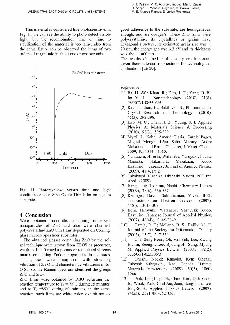
This material is considered like photosensitive. In Fig. 11 we can see the ability to photo detect visible light, but the recombination time or time to stabilization of the material is too large, also from the same figure can be observed the jump of two orders of magnitude in about one or two seconds.
0 300 600 900 1200
10-12
10-11
10-10
10-9
10-8
10-7
10-6
10-5
10-4
Light Dark
ZnO/Glass substrate
Dark
I (A
)
Tiempo (s)
Fig. 11 Photoresponse versus time and light conditions of our Zinc Oxide Thin Film on a glass substrate.
4 Conclusion Were obtained monoliths containing immersed nanoparticles of ZnO and also were obtained polycrystalline ZnO thin films deposited on Corning glass microscope slides substrates
The obtained glasses containing ZnO by the sol-gel technique were grown from TEOS as precursor, we think it is formed a porous or reticulated vitreous matrix containing ZnO nanoparticles in its pores. The glasses were amorphous, with stretching vibration of Zn-O and characteristic vibrations of Si-O-Si. So, the Raman spectrum identified the groups ZnO and SiO2. ZnO films were obtained by DBQ adjusting the reaction temperature to T1 = 75oC during 25 minutes and to T2 =85oC during 60 minutes, in the same reaction, such films are white color, exhibit not so
good adherence to the substrate, are homogeneous enough, and are opaque’s. These ZnO films were polycrystalline, its crystallites or grains have hexagonal structure, its estimated grain size was ~ 20 nm, the energy gap was 3.3 eV and its thickness was about 1000 nm. The results obtained in this study are important given their potential implications for technological applications [26-29]. References:
[1] Ra, H. -W.; Khan, R.; Kim, J. T.; Kang, B. R.; Im, Y. H. Nanotechnology (2010), 21(8), 085502/1-085502/5
[2] Ravichandran, K.; Sakthivel, B.; Philominathan, Crystal Research and Technology (2010), 45(3), 292-298.
[3] Kao, M. C.; Chen, H. Z.; Young, S. L Applied Physics A: Materials Science & Processing (2010), 98(3), 595-599.
[4] Myrtil L. Kahn, Arnaud Glaria, Carole Pages, Miguel Monge, Léna Saint Macary, André Maisonnat and Bruno Chaudret, J. Mater. Chem., 2009, 19, 4044 – 4060.
[5] Yamauchi, Hiroshi; Watanabe, Yasuyuki; Iizuka, Masaaki; Nakamura, Masakazu; Kudo, Kazuhiro. Japanese Journal of Applied Physics (2009), 48(4, Pt. 2)
[6] Takahashi, Hirohisa; Ishibashi, Satoru. PCT Int. Appl. (2009)
[7] Jiang, Hui; Toshima, Naoki. Chemistry Letters (2009), 38(6), 566-567
[8] Redinger, David; Subramanian, Vivek, IEEE Transactions on Electron Devices (2007), 54(6), 1301-1307
[9] Iechi, Hiroyuki; Watanabe, Yasuyuki; Kudo, Kazuhiro, Japanese Journal of Applied Physics, (2007), 46(4B), 2645-2649.
[10] Carcia, P. F.; McLean, R. S.; Reilly, M. H, Journal of the Society for Information Display (2005), 13(7), 547-554
[11] Cha, Sung Hoon; Oh, Min Suk; Lee, Kwang H.; Im, Seongil; Lee, Byoung H.; Sung, Myung M. Applied Physics Letters (2008), 92(2), 023506/1-023506/3
[12] Ohashi, Naoki; Kataoka, Ken; Ohgaki, Takeshi; Sakaguchi, Isao; Haneda, Hajime, Materials Transactions (2009), 50(5), 1060-1066
[13] Park, Jong-Lo; Park, Chan; Kim, Doh-Yeon; Jo, Wook; Park, Chul-Jae; Jeon, Sang-Yun; Lee, Jong-Sook. Applied Physics Letters (2009), 94(25), 252108/1-252108/3.
WSEAS TRANSACTIONS on CIRCUITS and SYSTEMS
S. J. Castillo, M. C. Acosta-Enriquez, Ma. E. Zayas, H. Arizpe, T. Mendivil-Reynoso, A. Garcia-Juarez, M. E. Alvarez-Ramos, E. Larios-Rodriguez
ISSN: 1109-2734 151 Issue 3, Volume 9, March 2010

[14] Lanyi Wang,w,z,y Guoyi Tang,z and Zheng-Kui Xuy J. Am. Ceram. Soc., (2008), 91 [11] 3742–3745.
[15] Gurvan Brasse, Christine Restoin, Jean-Louis Auguste, Philippe Roy, Stephanie Leparmentier, Jean-Marc Blondy, 1st WSEAS International Conference on Recent Advances in Nanotechnology Proceedings, ISSN: 1790-5117, ISBN: 978-960-474-059-8, (2009), 41-46.
[16] Suresh C. Pillai,a John M. Kelly,*b Declan E. McCormack*c and Raghavendra Rameshd, J. Mater. Chem., 2008, 18, 3926–3932
[17] C. X. Xu and X. W. Sun Applied Physics Letters 85, 17
[18] Adamopoulos, George; Bashir, Aneeqa; Woebkenberg, Paul H.; Bradley, Donal D. C.; Anthopoulos, Thomas D, Applied Physics Letters (2009), 95(13), 133507/1-133507/3.
[19] Bruni, F. Cariati, M. Casu, A. Lai, A. Musiu, G. Piccaluga and S. Solinas Nanostruct. Mater ., 1999, 11, 573.
[20] E. J. Kamitsos and A. P. Patsis, Phys. Rev. B, 1993, 48, 12499.
[21] H. Itzutzu, P. K. Hair, Y. Kiyozumi and F. Mizwkami, Mater. Res. Bull., 1997, 32, 1303.
[22] O. Clause, M. Kermarec, L. Bonneviot, F. Villain and M. Che, J. Am. Chem. Soc., 1992, 114, 4709.
[23] X. L. Xu, S. P. Lau, J. S. Chen, G. Y. Chen, B. K. Tay, J. of Crystal Growth 223 (2001) 201-205.
[24] N. B. Colthup, L. H. Daly, S. E. Wiberley Introduction to Infrared and Raman Spectroscopy, Ac. Press (1990).
[25] B-M. Basol, o.M Stafsudd, A Bindal, Sola Cells, 1985, 15, 279-284.
[26] Ana Marija Grancaric, Anita Tarbuk, Ivancica Kovacek, 1st WSEAS International Conference on Recent Advances in Nanotechnology, ISSN: 1790-5117, ISBN: 978-960-474-059-8 (2009), 21-23.
[27] H. Abdullah, S. Shaari, A.Amir Kadhum and M. N. Norazia, Proceedings of the 1st WSEAS International Conference on MATERIALS SCIENCE, ISSN: 1790-2769, ISBN: 978-960-474-024-6, (2008), 29-34.
[28] Huda Abdullah, Nugroho Pratomo Ariyanto, Brian Yuliarto and Syarif Junaid, Proceedings of the 1st WSEAS International Conference on MATERIALS SCIENCE, ISSN: 1790-2769, ISBN: 978-960-474-024-6, (2008), 24-48.
[29] S.J. Castillo, L.E. Regalado, M.R. Manzo-Valencia, J.C. Lopez-Cervantes, M.E. Alvarez-Ramos, A. Apolinar-Iribe and R.P. Duarte-Zamorano. New Nanotechnology
Development. ISBN: 978-1-60741-028-7. 2009 (pp. 17-30).
WSEAS TRANSACTIONS on CIRCUITS and SYSTEMS
S. J. Castillo, M. C. Acosta-Enriquez, Ma. E. Zayas, H. Arizpe, T. Mendivil-Reynoso, A. Garcia-Juarez, M. E. Alvarez-Ramos, E. Larios-Rodriguez
ISSN: 1109-2734 152 Issue 3, Volume 9, March 2010