Embed Size (px)
Citation preview

For the exclusive use of adopters of the book Introduction to Microelectronic Fabrication, Second Edition by Richard C. Jaeger. ISBN0-201-44494-1.
© 2002 Pearson Education, Inc., Upper Saddle River, NJ. All rights reserved. This material is protected under all copyright laws as they currently exist. No portion of this material may be reproduced, in any form or by any means, without permission in writing from the publisher.
Introduction toMicroelectronic Fabrication
by Richard C. Jaeger
Distinguished University ProfessorECE Department
Auburn University Chapter 6
Film Deposition

For the exclusive use of adopters of the book Introduction to Microelectronic Fabrication, Second Edition by Richard C. Jaeger. ISBN0-201-44494-1.
© 2002 Pearson Education, Inc., Upper Saddle River, NJ. All rights reserved. This material is protected under all copyright laws as they currently exist. No portion of this material may be reproduced, in any form or by any means, without permission in writing from the publisher.
Copyright Notice
• © 2002 Pearson Education, Inc., Upper Saddle River, NJ. All rights reserved. This material is protected under all copyright laws as they currently exist. No portion of this material may be reproduced, in any form or by any means, without permission in writing from the publisher.
• For the exclusive use of adopters of the book Introduction to Microelectronic Fabrication, Second Edition by Richard C. Jaeger. ISBN0-201-44494-1.

For the exclusive use of adopters of the book Introduction to Microelectronic Fabrication, Second Edition by Richard C. Jaeger. ISBN0-201-44494-1.
© 2002 Pearson Education, Inc., Upper Saddle River, NJ. All rights reserved. This material is protected under all copyright laws as they currently exist. No portion of this material may be reproduced, in any form or by any means, without permission in writing from the publisher.
EvaporationHigh Vacuum System

For the exclusive use of adopters of the book Introduction to Microelectronic Fabrication, Second Edition by Richard C. Jaeger. ISBN0-201-44494-1.
© 2002 Pearson Education, Inc., Upper Saddle River, NJ. All rights reserved. This material is protected under all copyright laws as they currently exist. No portion of this material may be reproduced, in any form or by any means, without permission in writing from the publisher.
EvaporationFilament & Electron Beam
(a) Filament Evaporation with Loops of Wire Hanging from a Heated Filament
(b) Electron Beam is Focused on Metal Charge by a Magnetic Field
For the exclusive use of adopters of the book Introduction to Microelectronic Fabrication, Second Edition by Richard C. Jaeger. ISBN0-201-44494-1.
© 2002 Pearson Education, Inc., Upper Saddle River, NJ. All rights reserved. This material is protected under all copyright laws as they currently exist. No portion of this material may be reproduced, in any form or by any means, without permission in writing from the publisher.
EvaporationElectron Beam
€
Growth Rate
G =m
πρr2cosφcosθ
cosφ = cosθ =r
2ro
G =m
4πρro2

For the exclusive use of adopters of the book Introduction to Microelectronic Fabrication, Second Edition by Richard C. Jaeger. ISBN0-201-44494-1.
© 2002 Pearson Education, Inc., Upper Saddle River, NJ. All rights reserved. This material is protected under all copyright laws as they currently exist. No portion of this material may be reproduced, in any form or by any means, without permission in writing from the publisher.
EvaporationShadowing and Step Coverage
• Shadowing and Step Coverage Problems Can Occur in Low Pressure Vacuum Deposition in which the Mean Free Path is Large
Figure 6.5

For the exclusive use of adopters of the book Introduction to Microelectronic Fabrication, Second Edition by Richard C. Jaeger. ISBN0-201-44494-1.
© 2002 Pearson Education, Inc., Upper Saddle River, NJ. All rights reserved. This material is protected under all copyright laws as they currently exist. No portion of this material may be reproduced, in any form or by any means, without permission in writing from the publisher.
Film DepositionSputtering
Figure 6.6A dc sputtering system in which the target material acts as the cathode of a diode and the wafers are mounted on the system anode.
Figure 6.7Sputtering yield increases rapidly as ion energy is increased above the sputtering threshold (argon)
For the exclusive use of adopters of the book Introduction to Microelectronic Fabrication, Second Edition by Richard C. Jaeger. ISBN0-201-44494-1.
© 2002 Pearson Education, Inc., Upper Saddle River, NJ. All rights reserved. This material is protected under all copyright laws as they currently exist. No portion of this material may be reproduced, in any form or by any means, without permission in writing from the publisher.
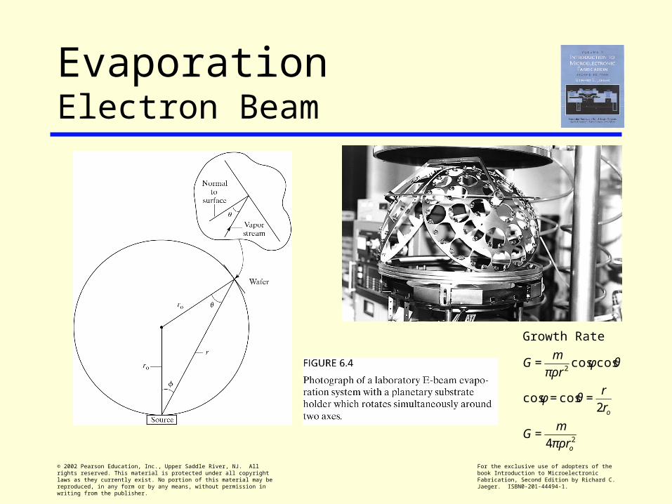
CVDChemical Vapor Deposition
Figure 6.8Four types of CVD systems. (a) Atmospheric-pressure reactor (b) hot-wall low-pressure (LPCVD) system in a three-zone furnace (c) parallel-plate plasma-enhanced system (d) photo-enhanced (PECVD) system using a three-zone furnace. Copyright 1983 Bell Telephone Laboratories, Inc. Reprinted with permission from Ref. [2].

For the exclusive use of adopters of the book Introduction to Microelectronic Fabrication, Second Edition by Richard C. Jaeger. ISBN0-201-44494-1.
© 2002 Pearson Education, Inc., Upper Saddle River, NJ. All rights reserved. This material is protected under all copyright laws as they currently exist. No portion of this material may be reproduced, in any form or by any means, without permission in writing from the publisher.
CVDPolysilicon Deposition
€
SiH4600o C ⏐ → ⏐ ⏐ Si + 2H2
•Low Pressure Chemical Vapor Deposition (LPCVD)
– 25-150 Pa
•Thermal Decomposition of Silane– 100% Silane– 20-30% Silane in Nitrogen
– 100-200 Å/min at 600-650o C
For the exclusive use of adopters of the book Introduction to Microelectronic Fabrication, Second Edition by Richard C. Jaeger. ISBN0-201-44494-1.
© 2002 Pearson Education, Inc., Upper Saddle River, NJ. All rights reserved. This material is protected under all copyright laws as they currently exist. No portion of this material may be reproduced, in any form or by any means, without permission in writing from the publisher.
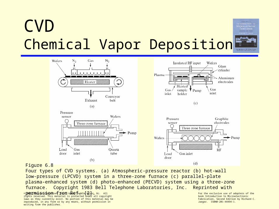
CVDSilicon Dioxide Deposition
€
Deposition of Silicon Dioxide over Aluminum (300 - 500 C)
SiH4 + O2 → SiO2 + 2H2 T ≤ 577oC
Phosphous Doped SiO2 - Atmospheric Pressure or LPCVD
4PH3 + 5O2 → 2P2O5 + 6H2
Higher Temperature Prior to Metallization
Dichlorosilane Reaction at 900oC
SiCl2H2 + 2N2O → SiO2 + 2N2 + 2HCl
LPCVD Decomposition of TEOS 650 - 750oC
Si OC2H5( )4→ SiO2 +byproducts
SiO2 containing 6-8% phosphorus will soften and flow at 1000-1100o C.
“P-glass reflow” can be used to smooth surface topology.
For the exclusive use of adopters of the book Introduction to Microelectronic Fabrication, Second Edition by Richard C. Jaeger. ISBN0-201-44494-1.
© 2002 Pearson Education, Inc., Upper Saddle River, NJ. All rights reserved. This material is protected under all copyright laws as they currently exist. No portion of this material may be reproduced, in any form or by any means, without permission in writing from the publisher.
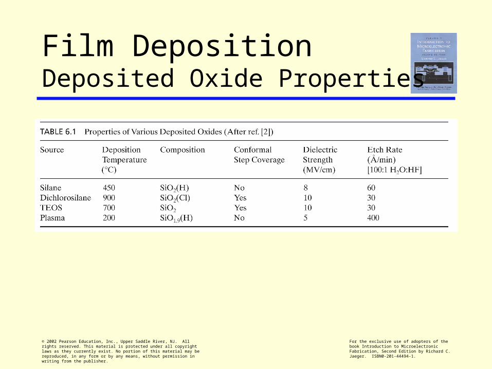
Film DepositionDeposited Oxide Properties
For the exclusive use of adopters of the book Introduction to Microelectronic Fabrication, Second Edition by Richard C. Jaeger. ISBN0-201-44494-1.
© 2002 Pearson Education, Inc., Upper Saddle River, NJ. All rights reserved. This material is protected under all copyright laws as they currently exist. No portion of this material may be reproduced, in any form or by any means, without permission in writing from the publisher.
CVDSilicon Nitride
€
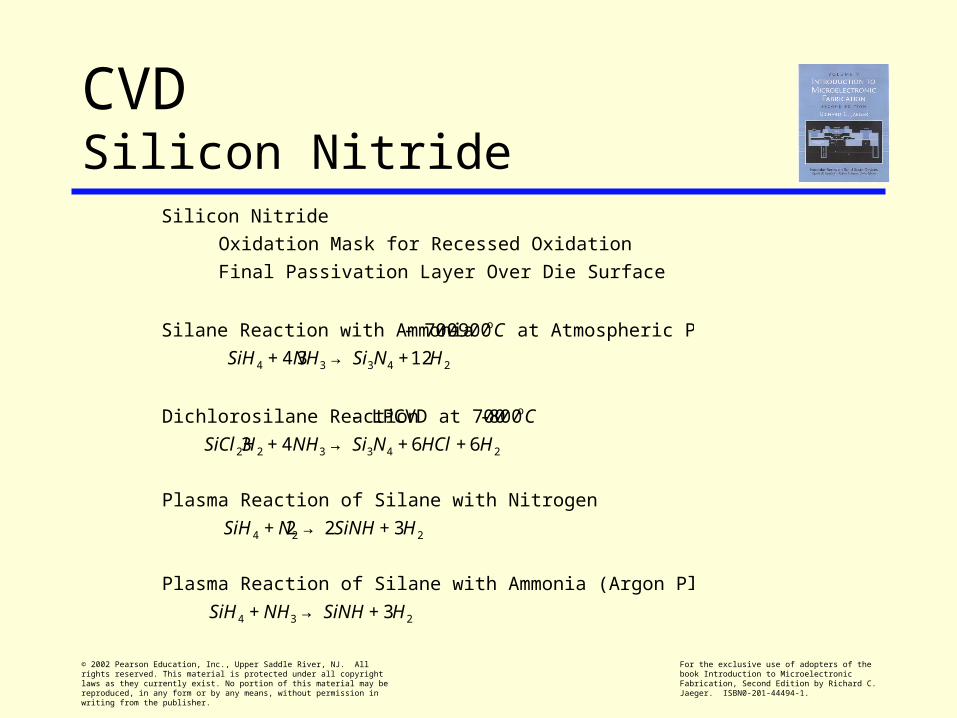
Silicon Nitride
Oxidation Mask for Recessed Oxidation
Final Passivation Layer Over Die Surface
Silane Reaction with Ammonia - 700 - 900oC at Atmospheric Pressure
3SiH4 + 4NH3 → Si3N4 +12H2
Dichlorosilane Reaction - LPCVD at 700 - 800oC
3SiCl2H2 + 4NH3 → Si3N4 + 6HCl + 6H2
Plasma Reaction of Silane with Nitrogen
2SiH4 + N2 → 2SiNH + 3H2
Plasma Reaction of Silane with Ammonia (Argon Plasma)
SiH4 + NH3 → SiNH + 3H2

For the exclusive use of adopters of the book Introduction to Microelectronic Fabrication, Second Edition by Richard C. Jaeger. ISBN0-201-44494-1.
© 2002 Pearson Education, Inc., Upper Saddle River, NJ. All rights reserved. This material is protected under all copyright laws as they currently exist. No portion of this material may be reproduced, in any form or by any means, without permission in writing from the publisher.
CVDMetal Deposition (Mo, Ta, Ti, W)
€
Tungsten - Thermal, Plasma or Optical Assisted Decomposition of WF6
WF6 →W + 3F2
Tungsten - Reduction of WF6 with Hydrogen
WF6 + 3H2 →W + 6HF
Mo, Ta and Ti - LPCVD Reaction with Hydrogen
2MCl5 + 5H2 → 2M +10HCl
− − − − − −
Copper is Deposited by "Standard" Plating Techniques

For the exclusive use of adopters of the book Introduction to Microelectronic Fabrication, Second Edition by Richard C. Jaeger. ISBN0-201-44494-1.
© 2002 Pearson Education, Inc., Upper Saddle River, NJ. All rights reserved. This material is protected under all copyright laws as they currently exist. No portion of this material may be reproduced, in any form or by any means, without permission in writing from the publisher.
Film Deposition Epitaxial Growth
• Vapor Phase Epitaxy
• Liquid Phase Epitaxy– Compound Semiconductors
• Molecular Beam Epitaxy– Compound Semiconductors
• III-V Compound Semiconductors– GaAs, InP, GaInAs, InAs …
For the exclusive use of adopters of the book Introduction to Microelectronic Fabrication, Second Edition by Richard C. Jaeger. ISBN0-201-44494-1.
© 2002 Pearson Education, Inc., Upper Saddle River, NJ. All rights reserved. This material is protected under all copyright laws as they currently exist. No portion of this material may be reproduced, in any form or by any means, without permission in writing from the publisher.
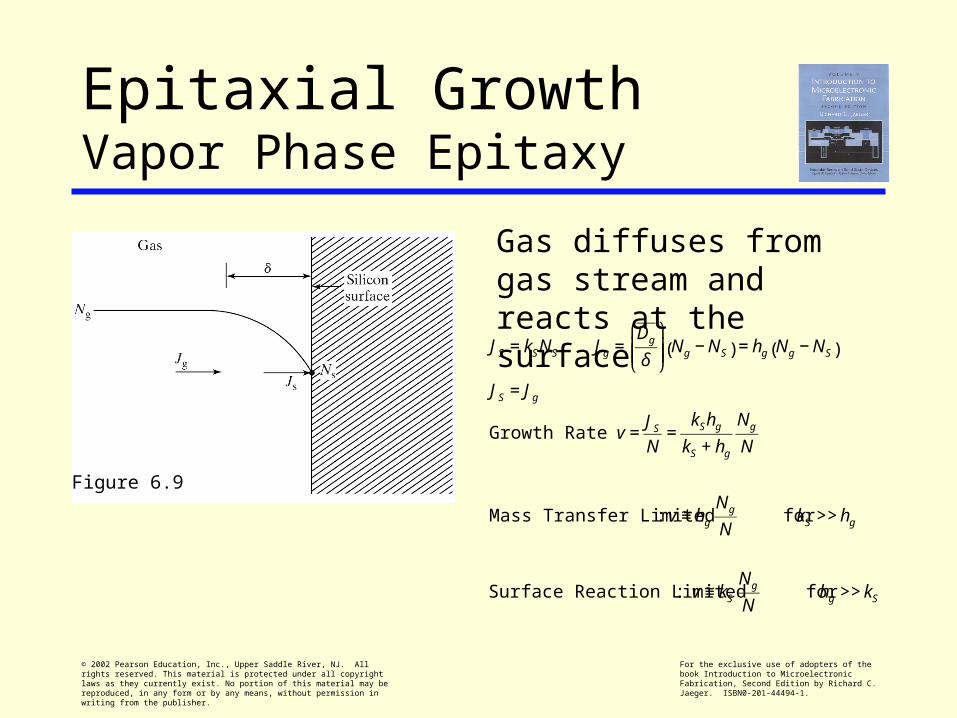
Epitaxial GrowthVapor Phase Epitaxy
€
JS = kSNS Jg =Dg
δ
⎛
⎝ ⎜ ⎜
⎞
⎠ ⎟ ⎟ Ng − NS( ) = hg Ng − NS( )
JS = Jg
Growth Rate v =JS
N=
kShg
kS + hg
Ng
N
Mass Transfer Limited : v ≅ hg
Ng
N for kS >> hg
Surface Reaction Limited : v ≅ kS
Ng
N for hg >> kS
Figure 6.9
Gas diffuses from gas stream and reacts at the surface
For the exclusive use of adopters of the book Introduction to Microelectronic Fabrication, Second Edition by Richard C. Jaeger. ISBN0-201-44494-1.
© 2002 Pearson Education, Inc., Upper Saddle River, NJ. All rights reserved. This material is protected under all copyright laws as they currently exist. No portion of this material may be reproduced, in any form or by any means, without permission in writing from the publisher.
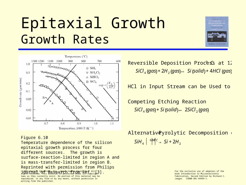
Epitaxial GrowthGrowth Rates
Figure 6.10Temperature dependence of the silicon epitaxial growth process for four different sources. The growth is surface-reaction-limited in region A and is mass-transfer-limited in region B. Reprinted with permission from Philips Journal of Research from Ref. [3]. €
Reversible Deposition Process at 1200o C
SiCl4 gas( ) + 2H2 gas( ) ↔ Si solid( ) + 4HCl gas( )
HCl in Input Stream can be Used to Clean Surface
Competing Etching Reaction
SiCl4 gas( ) + Si solid( ) ↔ 2SiCl2 gas( )
Alternative - Pyrolytic Decomposition of Silane
SiH4600o C ⏐ → ⏐ ⏐ Si + 2H2
For the exclusive use of adopters of the book Introduction to Microelectronic Fabrication, Second Edition by Richard C. Jaeger. ISBN0-201-44494-1.
© 2002 Pearson Education, Inc., Upper Saddle River, NJ. All rights reserved. This material is protected under all copyright laws as they currently exist. No portion of this material may be reproduced, in any form or by any means, without permission in writing from the publisher.
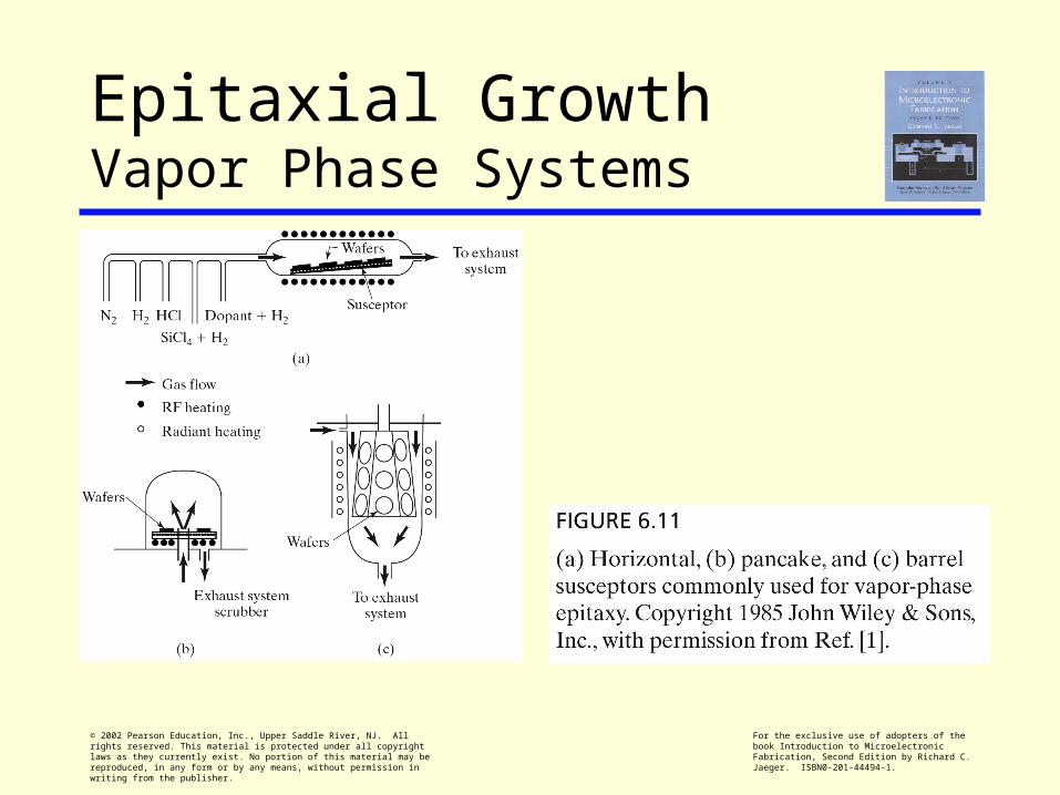
Epitaxial GrowthVapor Phase Systems

For the exclusive use of adopters of the book Introduction to Microelectronic Fabrication, Second Edition by Richard C. Jaeger. ISBN0-201-44494-1.
© 2002 Pearson Education, Inc., Upper Saddle River, NJ. All rights reserved. This material is protected under all copyright laws as they currently exist. No portion of this material may be reproduced, in any form or by any means, without permission in writing from the publisher.
Epitaxial GrowthGrowth in Silicon Tetrachloride
Single Crystal Silicon Growth for Rates Below 2 m/min
Etching for High SiCl4 Concentrations

For the exclusive use of adopters of the book Introduction to Microelectronic Fabrication, Second Edition by Richard C. Jaeger. ISBN0-201-44494-1.
© 2002 Pearson Education, Inc., Upper Saddle River, NJ. All rights reserved. This material is protected under all copyright laws as they currently exist. No portion of this material may be reproduced, in any form or by any means, without permission in writing from the publisher.
Epitaxial GrowthImpurity Redistribution
€
Moving Boundary Diffusion Problem
D∂ 2N
∂x 2=
∂N
∂t+ vx
∂N
∂x
For the exclusive use of adopters of the book Introduction to Microelectronic Fabrication, Second Edition by Richard C. Jaeger. ISBN0-201-44494-1.
© 2002 Pearson Education, Inc., Upper Saddle River, NJ. All rights reserved. This material is protected under all copyright laws as they currently exist. No portion of this material may be reproduced, in any form or by any means, without permission in writing from the publisher.
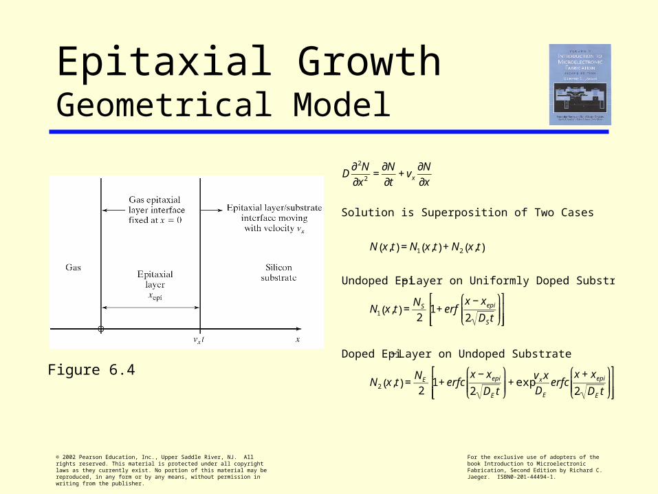
Epitaxial GrowthGeometrical Model
€
D∂ 2N
∂x 2=
∂N
∂t+ vx
∂N
∂x
Solution is Superposition of Two Cases
N x, t( ) = N1 x, t( ) + N2 x, t( )
Undoped Epi− Layer on Uniformly Doped Substrate
N1 x, t( ) =NS
21+ erf
x − xepi
2 DS t
⎛
⎝ ⎜ ⎜
⎞
⎠ ⎟ ⎟
⎡
⎣ ⎢ ⎢
⎤
⎦ ⎥ ⎥
Doped Epi − Layer on Undoped Substrate
N2 x, t( ) =NE
21+ erfc
x − xepi
2 DE t
⎛
⎝ ⎜ ⎜
⎞
⎠ ⎟ ⎟+ exp
vx x
DE
erfcx + xepi
2 DE t
⎛
⎝ ⎜ ⎜
⎞
⎠ ⎟ ⎟
⎡
⎣ ⎢ ⎢
⎤
⎦ ⎥ ⎥
Figure 6.4
For the exclusive use of adopters of the book Introduction to Microelectronic Fabrication, Second Edition by Richard C. Jaeger. ISBN0-201-44494-1.
© 2002 Pearson Education, Inc., Upper Saddle River, NJ. All rights reserved. This material is protected under all copyright laws as they currently exist. No portion of this material may be reproduced, in any form or by any means, without permission in writing from the publisher.
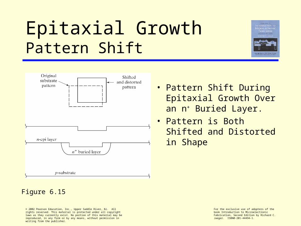
Epitaxial GrowthPattern Shift
• Pattern Shift During Epitaxial Growth Over an n+ Buried Layer.
• Pattern is Both Shifted and Distorted in Shape
Figure 6.15
For the exclusive use of adopters of the book Introduction to Microelectronic Fabrication, Second Edition by Richard C. Jaeger. ISBN0-201-44494-1.
© 2002 Pearson Education, Inc., Upper Saddle River, NJ. All rights reserved. This material is protected under all copyright laws as they currently exist. No portion of this material may be reproduced, in any form or by any means, without permission in writing from the publisher.
Film DeposiiontReferences & Further Reading
For the exclusive use of adopters of the book Introduction to Microelectronic Fabrication, Second Edition by Richard C. Jaeger. ISBN0-201-44494-1.
© 2002 Pearson Education, Inc., Upper Saddle River, NJ. All rights reserved. This material is protected under all copyright laws as they currently exist. No portion of this material may be reproduced, in any form or by any means, without permission in writing from the publisher.
End of Chapter 6