Embed Size (px)
Citation preview

FnIO-S System ODVA SPECIFICATION NSxNA9188_??.docDraft-revB Ethernet/IP Adapter (NA-9188) Page 1 of 61
FnIO S–Series: NA-9188
Ethernet/IP Adapter
DRAFT

FnIO-S System ODVA SPECIFICATION NSxNA9188_??.docDraft-revB Ethernet/IP Adapter (NA-9188) Page 2 of 61
DOCUMENT CHANGE SUMMARYREV. PAGES REMARKS DATE Editor
N/A New Document
Draft release 05/11/2005 Go, Samsug
Draft B Enable Input Run/Idle Header (Default)Enable Output Run/Idle Header (Default)
12/19/2008 Go, Samsug
DRAFT

FnIO-S System ODVA SPECIFICATION NSxNA9188_??.docDraft-revB Ethernet/IP Adapter (NA-9188) Page 3 of 61
Table of Contents1. FNBUS OVERVIEW ........................................................................................................................................ 6
1.1. FNBUS SYSTEM ................................................................................................................................................................. 6 1.2. FNBUS PIN DESCRIPTION ................................................................................................................................................... 7
2. ETHERNET/IP ADAPTER MODULE ........................................................................................................... 8 2.1. SHAPE ............................................................................................................................................................................... 8 2.2. ETHERNET/IP ADAPTER SPECIFICATION .............................................................................................................................. 9 2.3. LED INDICATOR ............................................................................................................................................................. 10
2.3.1. Module Status LED (MOD) ................................................................................................................................... 10 2.3.2. Network Status LED (NET) ................................................................................................................................... 10 2.3.3. Link/Active Status LED (LINK) ............................................................................................................................ 10 2.3.4. Expansion I/O Module Status LED (I/O) .............................................................................................................. 10 2.3.5. Field Power Status LED ......................................................................................................................................... 11 2.3.6. Adapter Electrical Interface ................................................................................................................................... 11
2.4. ETHERNET/IP IP-ADDRESS SETUP .................................................................................................................................... 12 2.4.1. IP-Address Setup using BOOTP ............................................................................................................................ 12
2.5. I/O PROCESS IMAGE MAP ............................................................................................................................................... 13 2.5.1. Example of Input Process Image Map ................................................................................................................... 14 2.5.2. Example of Output Process Image Map ................................................................................................................ 18
3. OBJECT MODELS ......................................................................................................................................... 20 3.1. SUPPORTED OBJECTS ....................................................................................................................................................... 20 3.2. IDENTITY OBJECT ............................................................................................................................................................ 21
3.2.1. Common Services ................................................................................................................................................. 21 3.2.2. Class Attributes ...................................................................................................................................................... 21 3.2.3. Instance Attributes ................................................................................................................................................. 21
3.3. MESSAGE ROUTER OBJECT .............................................................................................................................................. 23 3.3.1. Common Services ................................................................................................................................................. 23 3.3.2. Class Attributes ...................................................................................................................................................... 23 3.3.3. Instance Attributes ................................................................................................................................................. 23
3.4. ASSEMBLY OBJECT .......................................................................................................................................................... 24 3.4.1. Common Services ................................................................................................................................................. 24 3.4.2. Class Attributes ...................................................................................................................................................... 24 3.4.3. Instance Attributes ................................................................................................................................................. 24
3.5. CONNECTION MANAGER OBJECT ...................................................................................................................................... 25 3.5.1. Class Attributes, Instance Attribute ....................................................................................................................... 25
3.6. PORT OBJECT ................................................................................................................................................................. 25 3.6.1. Common Services ................................................................................................................................................. 25 3.6.2. Class Attributes ...................................................................................................................................................... 25 3.6.3. Instance Attributes ................................................................................................................................................. 25
3.7. TCP/IP OBJECT ............................................................................................................................................................ 26 3.7.1. Common Services ................................................................................................................................................. 26 3.7.2. Class Attributes ...................................................................................................................................................... 26 3.7.3. Instance Attributes ................................................................................................................................................. 26
3.8. ETHERNET LINK OBJECT ................................................................................................................................................. 27 3.8.1. Common Services ................................................................................................................................................. 27 3.8.2. Class Attributes ...................................................................................................................................................... 27 3.8.3. Instance Attributes ................................................................................................................................................. 27
3.9. FNBUS MANAGER OBJECT ............................................................................................................................................... 28
DRAFT

FnIO-S System ODVA SPECIFICATION NSxNA9188_??.docDraft-revB Ethernet/IP Adapter (NA-9188) Page 4 of 61
3.9.1. Common Services ................................................................................................................................................. 28 3.9.2. Class Attributes ...................................................................................................................................................... 28 3.9.3. Instance Attributes ................................................................................................................................................. 28
Table 3.9.1. Selection of Input (Produced) Process Image Mode..............................................................................29 Table 3.9.2. Selection of Output (Consumed) Process Image Mode.........................................................................29 Table 3.9.3. Slot Active Flag....................................................................................................................................29 Table 3.9.4. Slot Live List.........................................................................................................................................29 Table 3.9.5. Slot Alarm List......................................................................................................................................30 Table 3.9.6. External IDs (=Expansion Module ID).................................................................................................30
3.10. EXPANSION SLOT OBJECT .............................................................................................................................................. 31 3.10.1. Common Services ............................................................................................................................................... 31 3.10.2. Class Attributes .................................................................................................................................................... 31 3.10.3. Instance Attributes ............................................................................................................................................... 31
Table 3.10.1. I/O Data Code Format.........................................................................................................................32 Table 3.10.2. Product Code Format..........................................................................................................................32
3.11. ETHERNET/IP REFERENCE ............................................................................................................................................. 35
APPENDIX A.....................................................................................................................................................36A.1. PRODUCT LIST...............................................................................................................................................................36A.2. CONFIGURATION PARAMETER.........................................................................................................................................38
A.2.1. ST-1214 (4-sinking input, 24Vdc)........................................................................................................................38A.2.2. ST-1224 (4-sourcing input, 24Vdc)......................................................................................................................38A.2.3. ST-1218 (8-sinking input, 24Vdc)........................................................................................................................38A.2.4. ST-1228 (8-sourcing input, 24Vdc)......................................................................................................................38A.2.5. ST-121F (16-sinking input, 24Vdc)......................................................................................................................38A.2.6. ST-122F (16-sourcing input, 24Vdc)....................................................................................................................38A.2.7. ST-1314 (4-sinking input, 48Vdc)........................................................................................................................38A.2.8. ST-1324 (4-sourcing input, 48Vdc)......................................................................................................................38A.2.9. ST-1804 (4-ac input, 110Vac)...............................................................................................................................38A.2.10. ST-1904 (4-ac input, 220Vac).............................................................................................................................38A.2.11. ST-2314 (4-sinking output, 24Vdc 0.5A)...........................................................................................................39A.2.12. ST-2324 (4-sourcing output, 24Vdc 0.5A).........................................................................................................39A.2.13. ST-2318 (8-sinking output, 24Vdc 0.5A)...........................................................................................................39A.2.14. ST-2328 (8-sourcing output, 24Vdc 0.5A).........................................................................................................41A.2.15. ST-221F (16-sinking output, 24Vdc 0.3A).........................................................................................................41A.2.16. ST-222F (16-sourcing output, 24Vdc 0.3A).......................................................................................................41A.2.17. ST-2414 (4-sinking output, Diag, 24Vdc 0.5A).................................................................................................42A.2.18. ST-2424 (4-sourcing output, Diag, 24Vdc 0.5A)...............................................................................................42A.2.19. ST-2514 (4-sinking output, Diag, 24Vdc 2A)....................................................................................................42A.2.20. ST-2524 (4-sourcing output, Diag, 24Vdc 2A)..................................................................................................43A.2.21. ST-2742 (2-relay output, 230Vac 2A)................................................................................................................43A.2.22. ST-2852 (2-triac output, 120Vac 0.5A)..............................................................................................................43A.2.23. ST-3114 (4-current analog input, 0~20mA, 12bit).............................................................................................44A.2.24. ST-3134 (4-current analog input, 0~20mA, 14bit).............................................................................................44A.2.25. ST-3214 (4-current analog input, 4~20mA, 12bit).............................................................................................44A.2.26. ST-3234 (4-current analog input, 4~20mA, 14bit).............................................................................................44A.2.27. ST-3424 (4-voltage analog input, 0~10V, 12bit)................................................................................................44A.2.28. ST-3444 (4-voltage analog input, 0~10V, 14bit)................................................................................................44A.2.29. ST-3524 (4-voltage analog input, -10~10V, 12bit).............................................................................................44A.2.30. ST-3544 (4-voltage analog input, -10~10V, 14bit).............................................................................................44A.2.31. ST-3624 (4-voltage analog input, 0~5V, 12bit)..................................................................................................44A.2.32. ST-3644 (4-voltage analog input, 0~5V, 14bit)..................................................................................................44A.2.33. ST-3702 (2- RTD/Resistance input)...................................................................................................................46
DRAFT
FnIO-S System ODVA SPECIFICATION NSxNA9188_??.docDraft-revB Ethernet/IP Adapter (NA-9188) Page 5 of 61
A.2.34. ST-3802 (2- Thermocouple/mV input)...............................................................................................................47A.2.35. ST-4112 (2-current analog output, 0~20mA, 12bit)...........................................................................................48A.2.36. ST-4212 (2-current analog output, 4~20mA, 12bit)...........................................................................................48A.2.37. ST-4422 (2-voltage analog output, 0~10Vdc, 12bit)..........................................................................................48A.2.38. ST-4522 (2-voltage analog output, -10~10Vdc, 12bit).......................................................................................48A.2.39. ST-4622 (2-voltage analog output, 0~5Vdc, 12bit)............................................................................................48A.2.40. ST-5101 (1 Channel High Speed Counter 5Vdc)...............................................................................................48A.2.41. ST-5111 (1 Channel High Speed Counter 24Vdc).............................................................................................48
A.3. MEMORY REGISTER.......................................................................................................................................................49A.3.1. ST-1214 (4-sinking input, 24Vdc)........................................................................................................................49A.3.2. ST-1224 (4-sourcing input, 24Vdc)......................................................................................................................49A.3.3. ST-1218 (8-sinking input, 24Vdc)........................................................................................................................49A.3.4. ST-1228 (8-sourcing input, 24Vdc)......................................................................................................................49A.3.5. ST-121F (16-sinking input, 24Vdc)......................................................................................................................49A.3.6. ST-122F (16-sourcing input, 24Vdc)....................................................................................................................49A.3.7. ST-1314 (4-sinking input, 48Vdc)........................................................................................................................49A.3.8. ST-1324 (4-sourcing input, 48Vdc)......................................................................................................................49A.3.9. ST-1804 (4-ac input, 110Vac)...............................................................................................................................49A.3.10. ST-1904 (4-ac input, 220Vac).............................................................................................................................49A.3.11. ST-2314 (4-sinking output, 24Vdc 0.5A)...........................................................................................................49A.3.12. ST-2324 (4-sourcing output, 24Vdc 0.5A).........................................................................................................50A.3.13. ST-2318 (8-sinking output, 24Vdc 0.5A)...........................................................................................................50A.3.14. ST-2328 (8-sourcing output, 24Vdc 0.5A).........................................................................................................50A.3.15. ST-221F (16-sinking output, 24Vdc 0.1A).........................................................................................................50A.3.16. ST-222F (16-sourcing output, 24Vdc 0.1A).......................................................................................................50A.3.17. ST-2414 (4-sinking output, Diag, 24Vdc 0.5A).................................................................................................50A.3.18. ST-2424 (4-sourcing output, Diag, 24Vdc 0.5A)...............................................................................................50A.3.19. ST-2514 (4-sinking output, Diag, 24Vdc 2A)....................................................................................................50A.3.20. ST-2524 (4-sourcing output, Diag, 24Vdc 2A)..................................................................................................50A.3.21. ST-2742 (2-relay output, 230Vac 2A)................................................................................................................50A.3.22. ST-2852 (2-triac output, 120Vac 0.5A)..............................................................................................................50A.3.23. ST-3114 (4-current analog input, 0~20mA, 12bit).............................................................................................51A.3.24. ST-3134 (4-current analog input, 0~20mA, 14bit).............................................................................................51A.3.25. ST-3214 (4-current analog input, 4~20mA, 12bit).............................................................................................52A.3.26. ST-3234 (4-current analog input, 4~20mA, 14bit).............................................................................................52A.3.27. ST-3424 (4-voltage analog input, 0~10V, 12bit)................................................................................................53A.3.28. ST-3444 (4-voltage analog input, 0~10V, 14bit)................................................................................................53A.3.29. ST-3524 (4-voltage analog input, -10~10V, 12bit).............................................................................................54A.3.30. ST-3544 (4-voltage analog input, -10~10V, 14bit).............................................................................................54A.3.31. ST-3624 (4-voltage analog input, 0~5V, 12bit)..................................................................................................55A.3.32. ST-3644 (4-voltage analog input, 0~5V, 14bit)..................................................................................................55A.3.33. ST-3702 (2- RTD/Resistance input)...................................................................................................................56A.3.34. ST-3802 (2- Thermocouple/mV input)...............................................................................................................56A.3.35. ST-4112 (2-current analog output, 0~20mA, 12bit)...........................................................................................58A.3.36. ST-4212 (2-current analog output, 4~20mA, 12bit)...........................................................................................58A.3.37. ST-4422 (2-voltage analog output, 0~10Vdc, 12bit)..........................................................................................59A.3.38. ST-4522 (2-voltage analog output, -10~10Vdc, 12bit).......................................................................................59A.3.39. ST-4622 (2-voltage analog output, 0~5Vdc, 12bit)...........................................................................................60A.3.40. ST-5101 (1 Channel High Speed Counter 5Vdc)...............................................................................................60A.3.41. ST-5111 (1 Channel High Speed Counter 24Vdc).............................................................................................60
DRAFT

FnIO-S System ODVA SPECIFICATION NSxNA9188_??.docDraft-revB Ethernet/IP Adapter (NA-9188) Page 6 of 61
1. FNBUS OVERVIEW
1.1. FnBus System
Network Adapter ModuleThe Network Adapter Module forms the link between the fieldbus and the field devices with the Expansion Modules. The connection to different fieldbus systems can be established by each of the corresponding Network Adapter Module, e.g. for SynqNet, PROFIBUS, CANopen, DeviceNet , Ethernet/IP, CC-Link, MODBUS/Serial, MODBUS/TCP etc.
Expansion ModuleThe Expansion Modules are supported a variety of input and output field devices. There are digital and analog input/output modules and special function modules.
Two types of FnBus Message Service Messaging I/O Messaging
DRAFT
NetworkAdapterModule
GNDToken OutputSerial OutputSerial InputReserved
Ethernet/I
Profibus Slot 1 Slot 2 Slot 32
Vcc(5V)
Field GND (0Vdc)Field Vcc (24Vdc)
…
…
NetworkAdapterModule
ExpansionModule
...
DeviceNe
CANope

FnIO-S System ODVA SPECIFICATION NSxNA9188_??.docDraft-revB Ethernet/IP Adapter (NA-9188) Page 7 of 61
1.2. FnBus Pin Description
No. Name Description1 Vcc System supply voltage (5V dc).2 GND System Ground.3 Token Output Token output port of Processor module.4 Serial Output Transmitter output port of Processor module.5 Serial Input Receiver input port of Processor module.6 Reserved Reserved for bypass Token.
7 Field GND Field Ground.8 Field Vcc Field supply voltage (24Vdc).
DRAFT

FnIO-S System ODVA SPECIFICATION NSxNA9188_??.docDraft-revB Ethernet/IP Adapter (NA-9188) Page 8 of 61
2. ETHERNET/IP ADAPTER MODULE
2.1. Shape
NA-9188 (Ethernet/IP)
DRAFT
FnBus
24V 0VSystem Power
24V 0VField Power
Field Power
EthernetRJ-45

FnIO-S System ODVA SPECIFICATION NSxNA9188_??.docDraft-revB Ethernet/IP Adapter (NA-9188) Page 9 of 61
2.2. Ethernet/IP Adapter Specification
SpecificationInterface Specification, NA-9188 (Ethernet/IP Adapter)Adapter Type Level 2 I/O Server (Explicit, I/O Message)Max. Expansion Module 32 slotsMax. Input Size 252 bytesMax. Output Size 252 bytesMax. Length Bus Line Up to100m from Ethernet Hub/Switch with twisted CAT 3 UTP/STPMax. Nodes Limited by Ethernet Specification.Max. Connection 16 IO message connections
64 CIP connections64 Explicit message connections
Data transfer rate 10/100Mbps, Auto-negotiation, Full duplex Protocol Ethernet/IP, BOOTPInterface Connector RJ-45 socketIP-Address Setup Via BOOTPIndicator 5 LEDs
1 Green/Red, Module Status (MOD)1 Green, Network Status (NET)1 Green, Link/Active Status (LINK)1 Green/Red Expansion I/O Module Status (I/O)1 Green, Field Power Status
Module Location Starter module – left side of FnIO systemField Power Detection About 11Vdc
General SpecificationSystem Power Supply voltage : 24Vdc nominal
Supply voltage range : 11~28.8VdcProtection : Output current limit(Min. 1.5A) Reverse polarity protection
Power Dissipation 60mA typical @24VdcCurrent for I/O Module 1.5A @5VdcIsolation System power to internal logic : Non-isolation
System power to I/O driver : IsolationField Power Supply voltage : 24Vdc nominal
Supply voltage range : 11~28.8VdcMax. Current Field PowerContact
DC 10A Max.
Weight 150gModule Size 45mm x 99mm x 70mmEnvironment Condition Refer to Environment Specification
DRAFT
FnIO-S System ODVA SPECIFICATION NSxNA9188_??.docDraft-revB Ethernet/IP Adapter (NA-9188) Page 10 of 61
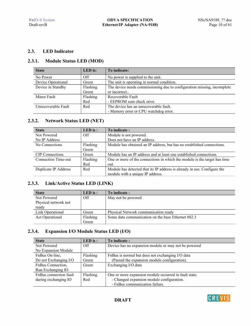
2.3. LED Indicator
2.3.1. Module Status LED (MOD)
State LED is: To indicate:No Power Off No power is supplied to the unit.Device Operational Green The unit is operating in normal condition.Device in Standby Flashing
GreenThe device needs commissioning due to configuration missing, incomplete or incorrect..
Minor Fault Flashing Red
Recoverable Fault- EEPROM sum check error.
Unrecoverable Fault Red The device has an unrecoverable fault. - Memory error or CPU watchdog error.
2.3.2. Network Status LED (NET)
State LED is : To indicate :Not PoweredNo IP Address
Off Module is not powered.Does not have an IP address.
No Connections Flashing Green
Module has obtained an IP address, but has no established connections.
CIP Connections Green Module has an IP address and at least one established connections.Connection Time-out Flashing
RedOne or more of the connections in which the module is the target has time out.
Duplicate IP Address Red Module has detected that its IP address is already in use. Configure the module with a unique IP address.
2.3.3. Link/Active Status LED (LINK)
State LED is : To indicate :Not PoweredPhysical network not ready
Off May not be powered
Link Operational Green Physical Network communication readyAct Operational Flashing
GreenSome data communication on the base Ethernet 802.3
2.3.4. Expansion I/O Module Status LED (I/O)
State LED is : To indicate :Not PoweredNo Expansion Module
Off Device has no expansion module or may not be powered
FnBus On-line,Do not Exchanging I/O
Flashing Green
FnBus is normal but does not exchanging I/O data(Passed the expansion module configuration).
FnBus Connection, Run Exchanging IO
Green Exchanging I/O data
FnBus connection fault during exchanging IO
Flashing Red
One or more expansion module occurred in fault state.- Changed expansion module configuration.- FnBus communication failure.
DRAFT

FnIO-S System ODVA SPECIFICATION NSxNA9188_??.docDraft-revB Ethernet/IP Adapter (NA-9188) Page 11 of 61
Expansion Configuration Failed
Red Failed to initialize expansion module- Detected invalid expansion module ID.- Overflowed Input/Output Size- Too many expansion module- Initial protocol failure- Mismatch vendor code between adapter and expansion module.
2.3.5. Field Power Status LED
State LED is : To indicate :Not Supplied Field Power Off Not supplied 24V dc field powerSupplied Field Power Green Supplied 24V dc field power
2.3.6. Adapter Electrical Interface
To connect the PC directly to network adapter without Hub(Switch), the Ethernet cable connection must be crossed.
Shielded RJ-45 Socket
DRAFT
RJ-45 SignalName
Description
1 TD+ Transmit +2 TD- Transmit +3 RD+ Receive +4 ----5 ----6 RD- Receive -7 ----8 ----
Case Shield
#1

FnIO-S System ODVA SPECIFICATION NSxNA9188_??.docDraft-revB Ethernet/IP Adapter (NA-9188) Page 12 of 61
2.4. Ethernet/IP IP-Address Setup
2.4.1. IP-Address Setup using BOOTP
If the adapter BOOTP enabled, the adapter sends BOOTP request message every 5sec.
The following is an example of adapter IP-Address setup that can be used with a third party BOOTP server.
Rockwell Automation’ s BOOTP server
DRAFT

FnIO-S System ODVA SPECIFICATION NSxNA9188_??.docDraft-revB Ethernet/IP Adapter (NA-9188) Page 13 of 61
2.5. I/O Process Image Map
An expansion module may have 3 types of data as I/O data, configuration parameter and memory register.The data exchange between network adapter and expansion modules is done via an I/O process image data by FnBus protocol. The following figure shows the data flow of process image between network adapter and expansion modules.
DRAFT
Write
Input Image Data
Slot 1 Input DataSlot 2 Input Data
Slot 32 Input Data
Output Image Data
Slot 1 Output DataSlot 2 Output Data
Slot 32 Output Data
Network Adapter
Network READ
Network WRITE
Slot 1
�Read
Slot 2 Slot 32
Expansion Modules
Status(Option)
FnIO-S System ODVA SPECIFICATION NSxNA9188_??.docDraft-revB Ethernet/IP Adapter (NA-9188) Page 14 of 61
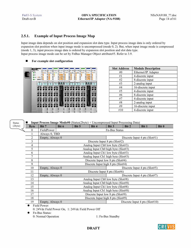
2.5.1. Example of Input Process Image Map
Input image data depends on slot position and expansion slot data type. Input process image data is only ordered by expansion slot position when input image mode is uncompressed (mode 0, 2). But, when input image mode is compressed (mode 1, 3), input process image data is ordered by expansion slot position and slot data type.Input process image mode can be set by FnBus Manager Object attribute#5. Refer to 3.9.
For example slot configuration
Input Process Image Mode#0 (Status(2byte) + Uncompressed Input Processing Data)Byte Bit 7 Bit 6 Bit 5 Bit 4 Bit 3 Bit 2 Bit 1 Bit 0
0 FieldPower Fn-Bus Status1 Always 0, TBD2 Empty, Always 0 Discrete Input 4 pts (Slot#1)3 Discrete Input 8 pts (Slot#2)4 Analog Input Ch0 low byte (Slot#3)5 Analog Input Ch0 high byte (Slot#3)6 Analog Input Ch1 low byte (Slot#3)7 Analog Input Ch1 high byte (Slot#3)8 Discrete Input low 8 pts (Slot#4)9 Discrete Input high 8 pts (Slot#4)10 Empty, Always 0 Discrete Input 4 pts (Slot#5)11 Discrete Input 8 pts (Slot#6)12 Empty, Always 0 Discrete Input 4 pts (Slot#7)13 Analog Input Ch0 low byte (Slot#8)14 Analog Input Ch0 high byte (Slot#8)15 Analog Input Ch1 low byte (Slot#8)16 Analog Input Ch1 high byte (Slot#8)17 Discrete Input low 8 pts (Slot#9)18 Discrete Input high 8 pts (Slot#9)19 Empty, Always 0 Discrete Input 4 pts (Slot#10)
Field Power: 0: 24Vdc Field Power On, 1: 24Vdc Field Power Off
Fn-Bus Status:0: Normal Operation 1: Fn-Bus Standby
DRAFT
Slot Address Module Description#0 Ethernet/IP Adapter#1 4-discrete input#2 8-discrete input#3 2-analog input#4 16-discrete input#5 4-discrete input#6 8-discrete input#7 4-discrete input#8 2-analog input#9 16-discrete input#10 4-discrete input
Status(2byte)

FnIO-S System ODVA SPECIFICATION NSxNA9188_??.docDraft-revB Ethernet/IP Adapter (NA-9188) Page 15 of 61
2: Fn-Bus Communication Fault 3: Slot Configuration Failed4: No Expansion Slot
DRAFT
FnIO-S System ODVA SPECIFICATION NSxNA9188_??.docDraft-revB Ethernet/IP Adapter (NA-9188) Page 16 of 61
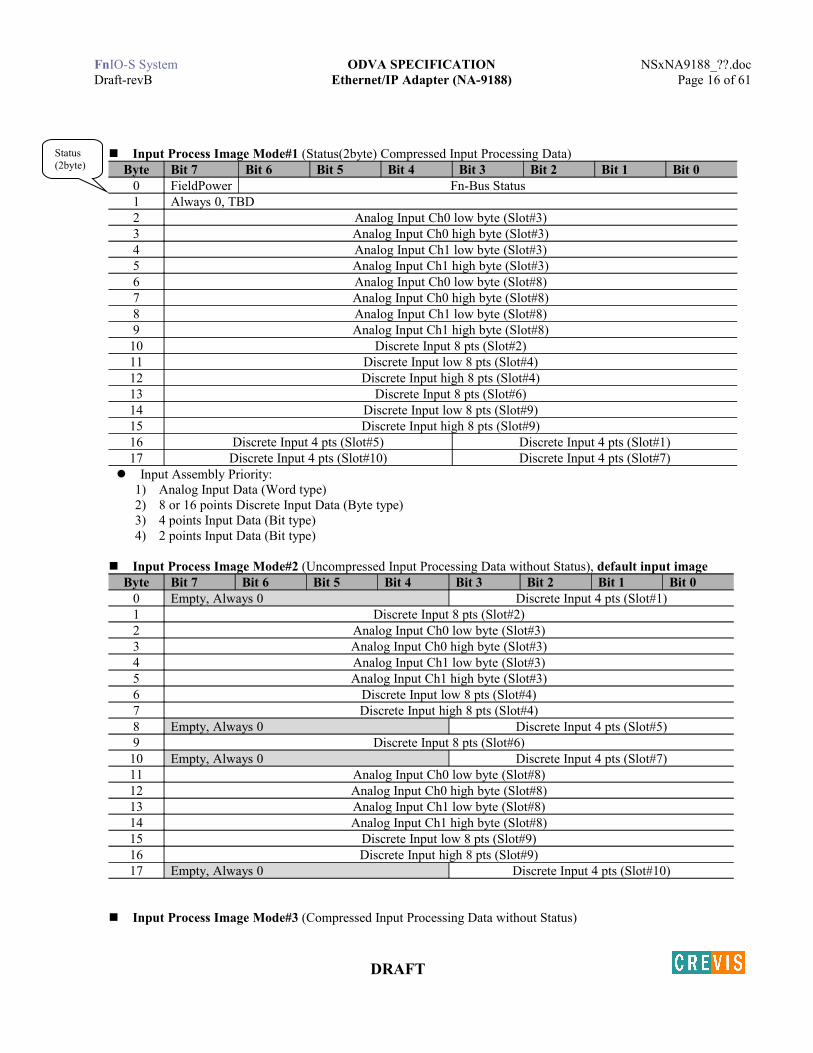
Input Process Image Mode#1 (Status(2byte) Compressed Input Processing Data)Byte Bit 7 Bit 6 Bit 5 Bit 4 Bit 3 Bit 2 Bit 1 Bit 0
0 FieldPower Fn-Bus Status1 Always 0, TBD2 Analog Input Ch0 low byte (Slot#3)3 Analog Input Ch0 high byte (Slot#3)4 Analog Input Ch1 low byte (Slot#3)5 Analog Input Ch1 high byte (Slot#3)6 Analog Input Ch0 low byte (Slot#8)7 Analog Input Ch0 high byte (Slot#8)8 Analog Input Ch1 low byte (Slot#8)9 Analog Input Ch1 high byte (Slot#8)10 Discrete Input 8 pts (Slot#2)11 Discrete Input low 8 pts (Slot#4)12 Discrete Input high 8 pts (Slot#4)13 Discrete Input 8 pts (Slot#6)14 Discrete Input low 8 pts (Slot#9)15 Discrete Input high 8 pts (Slot#9)16 Discrete Input 4 pts (Slot#5) Discrete Input 4 pts (Slot#1)17 Discrete Input 4 pts (Slot#10) Discrete Input 4 pts (Slot#7)
Input Assembly Priority: 1) Analog Input Data (Word type)2) 8 or 16 points Discrete Input Data (Byte type)3) 4 points Input Data (Bit type)4) 2 points Input Data (Bit type)
Input Process Image Mode#2 (Uncompressed Input Processing Data without Status), default input imageByte Bit 7 Bit 6 Bit 5 Bit 4 Bit 3 Bit 2 Bit 1 Bit 0
0 Empty, Always 0 Discrete Input 4 pts (Slot#1)1 Discrete Input 8 pts (Slot#2)2 Analog Input Ch0 low byte (Slot#3)3 Analog Input Ch0 high byte (Slot#3)4 Analog Input Ch1 low byte (Slot#3)5 Analog Input Ch1 high byte (Slot#3)6 Discrete Input low 8 pts (Slot#4)7 Discrete Input high 8 pts (Slot#4)8 Empty, Always 0 Discrete Input 4 pts (Slot#5)9 Discrete Input 8 pts (Slot#6)10 Empty, Always 0 Discrete Input 4 pts (Slot#7)11 Analog Input Ch0 low byte (Slot#8)12 Analog Input Ch0 high byte (Slot#8)13 Analog Input Ch1 low byte (Slot#8)14 Analog Input Ch1 high byte (Slot#8)15 Discrete Input low 8 pts (Slot#9)16 Discrete Input high 8 pts (Slot#9)17 Empty, Always 0 Discrete Input 4 pts (Slot#10)
Input Process Image Mode#3 (Compressed Input Processing Data without Status)
DRAFT
Status(2byte)

FnIO-S System ODVA SPECIFICATION NSxNA9188_??.docDraft-revB Ethernet/IP Adapter (NA-9188) Page 17 of 61
Byte Bit 7 Bit 6 Bit 5 Bit 4 Bit 3 Bit 2 Bit 1 Bit 00 Analog Input Ch0 low byte (Slot#3)1 Analog Input Ch0 high byte (Slot#3)2 Analog Input Ch1 low byte (Slot#3)3 Analog Input Ch1 high byte (Slot#3)4 Analog Input Ch0 low byte (Slot#8)5 Analog Input Ch0 high byte (Slot#8)6 Analog Input Ch1 low byte (Slot#8)7 Analog Input Ch1 high byte (Slot#8)8 Discrete Input 8 pts (Slot#2)9 Discrete Input low 8 pts (Slot#4)10 Discrete Input high 8 pts (Slot#4)11 Discrete Input 8 pts (Slot#6)12 Discrete Input low 8 pts (Slot#9)13 Discrete Input high 8 pts (Slot#9)14 Discrete Input 4 pts (Slot#5) Discrete Input 4 pts (Slot#1)15 Discrete Input 4 pts (Slot#10) Discrete Input 4 pts (Slot#7)
Input Assembly Priority: 1) Analog Input Data (Word type)2) 8 or 16 points Discrete Input Data (Byte type)3) 4 points Input Data (Bit type)4) 2 points Input Data (Bit type)
DRAFT
FnIO-S System ODVA SPECIFICATION NSxNA9188_??.docDraft-revB Ethernet/IP Adapter (NA-9188) Page 18 of 61
2.5.2. Example of Output Process Image Map
Output image data depends on slot position and expansion slot data type. Output process image data is only ordered by expansion slot position when output image mode is uncompressed (mode 0). But, when output image mode is compressed (mode 1), output process image data is ordered by expansion slot position and slot data type.Output process image mode can be set by FnBus Manager Object attribute#6. Refer to 3.9.
For example slot configuration
Output Process Image Mode#0 (Uncompressed Output Processing Data), default output imageByte Bit 7 Bit 6 Bit 5 Bit 4 Bit 3 Bit 2 Bit 1 Bit 0
0 Empty, Don’t care Discrete Output 4 pts (Slot#1)1 Discrete Output 8 pts (Slot#2)2 Analog Output Ch0 low byte (Slot#3)3 Analog Output Ch0 high byte (Slot#3)4 Analog Output Ch1 low byte (Slot#3)5 Analog Output Ch1 high byte (Slot#3)6 Discrete Output low 8 pts (Slot#4)7 Discrete Output high 8 pts (Slot#4)8 Empty, Don’t care Discrete Output 4 pts (Slot#5)9 Discrete Input 8 pts (Slot#6)10 Empty, Don’t care Discrete Output 2 pts
(Slot#7)11 Empty, Don’t care Discrete Output 2 pts
(Slot#8)12 Analog Output Ch0 low byte (Slot#9)13 Analog Output Ch0 high byte (Slot#9)14 Analog Output Ch1 low byte (Slot#9)15 Analog Output Ch1 high byte (Slot#9)16 Discrete Output low 8 pts (Slot#10)17 Discrete Output high 8 pts (Slot#10)18 Empty, Don’t care Discrete Output 4 pts (Slot#11)
Output Process Image Mode#1 (Compressed Output Processing Data)
DRAFT
Slot Address Module Description#0 Ethernet/IP Adapter#1 4-discrete output#2 8-discrete output#3 2-analog output#4 16-discrete output#5 4-discrete output#6 8-discrete output#7 2-realy output#8 2-realy output#9 2-analog output#10 16-discrete output#11 4-discrete output
FnIO-S System ODVA SPECIFICATION NSxNA9188_??.docDraft-revB Ethernet/IP Adapter (NA-9188) Page 19 of 61
Byte Bit 7 Bit 6 Bit 5 Bit 4 Bit 3 Bit 2 Bit 1 Bit 00 Analog Output Ch0 low byte (Slot#3)1 Analog Output Ch0 high byte (Slot#3)2 Analog Output Ch1 low byte (Slot#3)3 Analog Output Ch1 high byte (Slot#3)4 Analog Output Ch0 low byte (Slot#9)5 Analog Output Ch0 high byte (Slot#9)6 Analog Output Ch1 low byte (Slot#9)7 Analog Output Ch1 high byte (Slot#9)8 Discrete Output 8 pts (Slot#2)9 Discrete Output low 8 pts (Slot#4)10 Discrete Output high 8 pts (Slot#4)11 Discrete Input 8 pts (Slot#6)12 Discrete Output low 8 pts (Slot#10)13 Discrete Output high 8 pts (Slot#10)14 Discrete Output 4 pts (Slot#5) Discrete Output 4 pts (Slot#1)15 Discrete Output 2 pts
(Slot#8)Discrete Output 2 pts
(Slot#7)Discrete Output 4 pts (Slot#11)
Output Assembly Priority: 1) Analog Output Data (Word type)2) 8 or 16 points Discrete Output Data (Byte type)3) 4 points Output Data (Bit type)4) 2 points Output Data (Bit type)
DRAFT

FnIO-S System ODVA SPECIFICATION NSxNA9188_??.docDraft-revB Ethernet/IP Adapter (NA-9188) Page 20 of 61
3. OBJECT MODELSEvery CIP node is modeled as a collection of objects. An object provides an abstract representation of a particular component within a device. Anything not described in object form is not visible through the CIP protocol. CIP objects are structured into classes, instances, and attributes. A class of objects represents the same kind of system component. An object instance is the actual representation of a particular object within a class. Each instance of a class has the same attributes, but it has its own particular set of attribute values.
The objects and their components are addressed by a uniform addressing scheme consisting of : Media Access Control Identifier (MAC ID), an integer identification value assigned to each node on a CIP network. Class Identifier (Class ID), an integer identification value assigned to each Object Class accessible from the
network. Instance Identifier (Instance ID), an integer identification value assigned to an Object Instance that identifies it
among all Instances of the same Class. Attribute Identifier (Attribute ID), an integer identification value assigned to a Class and/or Instance Attribute. Service Code, an integer identification value which denotes a particular Object Instance and/or Object Class
function.
3.1. Supported Objects
Supported Object Name of Object Type Number of Instances Class CodeIdentity Required 1 01HEX
Message Router Required 1 02 HEX
Assembly Required 2 04 HEX
Connection Manager Required 1 06 HEX
Port Required 1 F4 HEX
TCP/IP Interface Required 1 F5 HEX
Ethernet Link Required 1 F6 HEX
FnBus Manager Vendor-specific 1 70 HEX
Expansion Slot Vendor-specific 1~32 71 HEX
DRAFT

FnIO-S System ODVA SPECIFICATION NSxNA9188_??.docDraft-revB Ethernet/IP Adapter (NA-9188) Page 21 of 61
3.2. Identity Object
Class Code: 01HEX
3.2.1. Common Services
Service Code
Implemented for Service Name ValueClass Instance
0x01 Yes Yes Get_Attribute_All0x05 No Yes Reset 0: Reset Only
1: Reset and Factory Default0x0E No Yes Get_Attribute_Single
3.2.2. Class Attributes
Instance ID
Attribute ID
Access Rule
Name Data Type Value
0 1 Get Revision UINT 0001HEX x
2 Get Max Instance UINT 0001HEX
6 Get Maximum ID Number Class Attributes
UINT 0000HEX
7 Get Maximum ID NumberInstance Attributes
UINT 0000HEX
3.2.3. Instance Attributes
Instance ID
Attribute ID
Access Rule
Name Data Type Value
1 1 Get Vendor ID UINT 741DEC (Crevis Co., Ltd)2 Get Device Type UINT 0CHEX (Communications Adapter)3 Get Product Code UINT 512 DEC (NA-9188)4 Get Revision
- Major- Minor
Structure of:USINTUSINT
1 ~ 91 ~ 255
5 Get Status WORD Defined in Spec.6 Get Serial Number UDINT Unique Number7 Get Product Name
- String Length- ASCII String
Short_StringUSINTSTRING
24DEC
“NA9188_Ethernet/IP_Adapter”Vendor-specific
100 Get Device Fault Code USINT 00HEX : Normal OperationBit 0: No expansion slotBit 1: Too many expansion slotBit 2: Overflow I/O sizeBit 3: I/O Configuration failure Bit 4: EEPROM Checksum faultBit 6: Invalid Module IDBit 7: Firmware fault
104 Get Firmware Release Date UDINT YYYYMMDDHEX
DRAFT

FnIO-S System ODVA SPECIFICATION NSxNA9188_??.docDraft-revB Ethernet/IP Adapter (NA-9188) Page 22 of 61
DRAFT

FnIO-S System ODVA SPECIFICATION NSxNA9188_??.docDraft-revB Ethernet/IP Adapter (NA-9188) Page 23 of 61
3.3. Message Router Object
Class Code: 02 HEX
3.3.1. Common Services
Service Code
Implemented for Service NameClass Instance
0x01 Yes No Get_Attribute_All0x0E No Yes Get_Attribute_Single
3.3.2. Class Attributes
Instance ID
Attribute ID
Access Rule
Name Data Type Value
0 1 Get Revision UINT 0001HEX
4 Get Number of Attribute UINT 0001HEX
5 Number of Service UINT 0000HEX
6 Get Maximum ID Number Class Attributes
UINT 0000HEX
7 Get Maximum ID NumberInstance Attributes
UINT 0000HEX
3.3.3. Instance Attributes
Instance ID
Attribute ID
Access Rule
Name Data Type Value
1 1 Get Object List STRUCT of UINT Array of
UINT
9DEC 01 00 02 00 04 00 06 00 F4 00 F5 00 F6 00 70 00 71 00
2 Get Number Available UINT 16DEC
Maximum number of connections supported
DRAFT

FnIO-S System ODVA SPECIFICATION NSxNA9188_??.docDraft-revB Ethernet/IP Adapter (NA-9188) Page 24 of 61
3.4. Assembly Object
Class Code: 04 HEX
3.4.1. Common Services
Service Code
Implemented for Service NameClass Instance
0x0E No Yes Get_Attribute_Single0x10 No Yes Set_Attribute_Single
3.4.2. Class Attributes
Instance ID
Attribute ID
Access Rule
Name Data Type Value
0 1 Get Revision UINT 0002HEX
2 Get Max Instance UINT
3.4.3. Instance Attributes
Instance ID
Attribute ID
Access Rule
Name Data Type Value
Input/ Output
Instance ID
3 Get/Set Data Array n BYTE
Input/Output process image data
Input/Output Instance IDInstance
IDAttribute
IDAccess Rule
Name Data Type Value
1(0x01)
3 Get Input (Produced) Process Image Data
Array n BYTE
Input process image data
2(0x02)
3 Set/Get Output (Consumed) Process Image Data
Array n BYTE
Output process image data
Configuration Instance is 170(AAHEX). There is no configuration data needed. Heartbeat Instance is 171(ABHEX) for input only connection. Listen only Instance is 172(ACHEX) for multicast listening.
DRAFT
FnIO-S System ODVA SPECIFICATION NSxNA9188_??.docDraft-revB Ethernet/IP Adapter (NA-9188) Page 25 of 61
3.5. Connection Manager Object
Class Code: 06 HEX
3.5.1. Class Attributes, Instance Attribute
None
3.6. Port Object
Class Code: F4hex
3.6.1. Common Services
Service Code
Implemented for Service NameClass Instance
0x01 Yes Yes Get_Attribute_All0x0E Yes Yes Get_Attribute_Single
3.6.2. Class Attributes
Instance ID
Attribute ID
Access Rule
Name Data Type Value
0 1 Get Revision UINT 0001HEX
2 Get Max Instance UINT 0001HEX
3 Get Num Instances UINT 0001HEX
8 Get Entry Port UINT 0001HEX
9 Get All Ports ARRY of STRUCT
UINTUINT
0000HEX
0000HEX
0004HEX
0002HEX
3.6.3. Instance Attributes
Instance ID
Attribute ID
Access Rule
Name Data Type Value
1 1 Get Port Type UINT 0004HEX , TCP/IP Port2 Get Port Number UINT 0002HEX, CIP port number associate
with port3 Get Port Object UINT
Padded EPATH
4 Get Port Name Short_String =07 Get Node Address Padded
EPATH
DRAFT
FnIO-S System ODVA SPECIFICATION NSxNA9188_??.docDraft-revB Ethernet/IP Adapter (NA-9188) Page 26 of 61
3.7. TCP/IP Object
Class Code: F5 HEX
3.7.1. Common Services
Service Code
Implemented for Service NameClass Instance
0x01 Yes Yes Get_Attribute_All0x0E Yes Yes Get_Attribute_Single0x02 No Yes Set_Attribute_All0x10 No Yes Set_Attribute_Single
3.7.2. Class Attributes
Instance ID
Attribute ID
Access Rule
Name Data Type Value
0 1 Get Revision UINT 0001HEX
2 Get Max Instance UINT 0001HEX
3 Get Num Instances UINT
3.7.3. Instance Attributes
Instance ID
Attribute ID
Access Rule
Name Data Type Value
1 1 Get Status DWORD2 Get Configuration
CapabilityDWORD 00000006HEX
3 Get/Set Configuration Control DWORD 00000010HEX
4 Get Physical Link PathSize of PathPath
STRUCT of:UINTPadded- PATH
0002HEX
20 F6 24 01
5 Get/Set Interface Configuration STRUCT of:UDINTUDINTUDINTUDINTUDINTSTRING
6 Get/Set HOST Name STRING
DRAFT

FnIO-S System ODVA SPECIFICATION NSxNA9188_??.docDraft-revB Ethernet/IP Adapter (NA-9188) Page 27 of 61
3.8. Ethernet Link Object
Class Code: F6 HEX
3.8.1. Common Services
Service Code
Implemented for Service NameClass Instance
0x01 Yes Yes Get_Attribute_All0x0E Yes Yes Get_Attribute_Single
3.8.2. Class Attributes
Instance ID
Attribute ID
Access Rule
Name Data Type Value
0 1 Get Revision UINT 0002HEX
2 Get Max Instance UINT 0001HEX
3 Get Num Instances UINT 0001HEX
3.8.3. Instance Attributes
Instance ID
Attribute ID
Access Rule
Name Data Type Value
1 1 Get Interface Speed UDINT 10DEC, 100DEC
2 Get Interface Flags DWORD Bit 0 : Link ActiveBit 1 : Full DuplexBit 2~4 : Auto negotiationBit 5 : Manual Setting required ResetBit 6 : Local Hardware FaultOthers : 0
3 Get Physical Address ARRAY of 6 USINTs
Same as MAC address
DRAFT

FnIO-S System ODVA SPECIFICATION NSxNA9188_??.docDraft-revB Ethernet/IP Adapter (NA-9188) Page 28 of 61
3.9. FnBus Manager Object
Class Code: 70 HEX
3.9.1. Common Services
Service Code
Implemented for Service NameClass Instance
0x0E No Yes Get_Attribute_Single0x10 No Yes Set_Attribute_Single
3.9.2. Class Attributes
None
3.9.3. Instance Attributes
Instance ID
Attribute ID
Access Rule
Name Data Type Value
1 1 Get Number of Slot USINT (include deactivated slot)2 Get Num of Activated Slot USINT3 Get Num of Deactivated
SlotUSINT
4 Get External IDs Array of 33 BYTE
See Table 3.9.6.See Appendix A.1.
5 Get/Set* Selection of Input (Produced) Process Image Mode
USINT See Table 3.9.1.Valid value range is 0,1,2,3(default 2)
6 Get/Set* Selection of Output (Consumed) Process Image Mode
USINT See Table 3.9.2.Valid value range is 0,1(default 0)
7 Get/Set* Slot Active Flag DWORD See Table 3.9.38 Get Slot Live List DWORD See Table 3.9.4.9 Get Slot Alarm List DWORD See Table 3.9.5.10 Get Fn-Bus Status USINT 0: Normal Operation
1: Fn-Bus Standby2: Fn-Bus Connection Fault3: Expansion Configuration Fault4: No Expansion Module
11 Get Input (Produced) Byte Size
UINT Read IO input data size
12 Get Output (Consumed) Byte Size
UINT Read IO output data size
13 Get/Set*TBD
Enable Input Run/IdleHeader (Default)
BOOL 0:Disabled1:Enabled Input Run/Idle Header
14 Get/Set*TBD
Enable Output Run/IdleHeader (Default)
BOOL 0:Disabled1:Enabled Output Run/Idle Header
32 Get Real IO Input Data Array n BYTE
Real IO input data
DRAFT

FnIO-S System ODVA SPECIFICATION NSxNA9188_??.docDraft-revB Ethernet/IP Adapter (NA-9188) Page 29 of 61
33 Get/Set Real IO Output Data Array n BYTE
Real IO output data
112 Set Scan Command Vendor only113 Get Run Time Fault Code Vendor only150 Get FnBus Revision UINT Vendor only151 Get Vendor Code USINT Vendor only224 Get All ST- name Array of
UINTsVendor only
226 Get Scan Time UINTUINT
Vendor only
*After the system is reset, the new “Set Value” action is applied.If changed slot location, set default value automatically.
Table 3.9.1. Selection of Input (Produced) Process Image Mode
Selection Input Image Mode
Description
0 Status(2byte) + Uncompressed Input Processing Data (default)1 Status(2byte) + Compressed Input Processing Data2 Uncompressed Input Processing Data default3 Compressed Input Processing Data
Table 3.9.2. Selection of Output (Consumed) Process Image Mode
Selection Output Image Mode
Description
0 Uncompressed Output Processing Data (default) default1 Compressed Output Processing Data
Table 3.9.3. Slot Active Flag
DWORD(32bits) Decimal Bit DescriptionGet/Set Bit 00 Activate/Deactivate flag for slot position #1 (0:Active, 1:Decative)
Bit 01 Activate/Deactivate flag for slot position #2 (0:Active, 1:Decative)Bit 02 Activate/Deactivate flag for slot position #3 (0:Active, 1:Decative)
.
.
.
.
.
.Bit 30 Activate/Deactivate flag for slot position #31 (0:Active, 1:Decative)Bit 31 Activate/Deactivate flag for slot position #32 (0:Active, 1:Decative)
Table 3.9.4. Slot Live List
DWORD(32bits) Decimal Bit DescriptionGet/Set Bit 00 This bit is set (1) when slot position #1 is available to exchange IO
Bit 01 This bit is set (1) when slot position #2 is available to exchange IOBit 02 This bit is set (1) when slot position #3 is available to exchange IO
.
.
.
.
.
.Bit 30 This bit is set (1) when slot position #31 is available to exchange IOBit 31 This bit is set (1) when slot position #32 is available to exchange IO
DRAFT

FnIO-S System ODVA SPECIFICATION NSxNA9188_??.docDraft-revB Ethernet/IP Adapter (NA-9188) Page 30 of 61
Table 3.9.5. Slot Alarm List
DWORD(32bits) Decimal Bit DescriptionGet/Set Bit 00 This bit is set (1) when an error is detected in slot position #1
Bit 01 This bit is set (1) when an error is detected in slot position #2Bit 02 This bit is set (1) when an error is detected in slot position #3
.
.
.
.
.
.Bit 30 This bit is set (1) when an error is detected in slot position #31Bit 31 This bit is set (1) when an error is detected in slot position #32
Table 3.9.6. External IDs (=Expansion Module ID)
Byte Description0 Network Adapter Module External ID = 0x001 External ID for slot position #12 External ID for slot position #23 External ID for slot position #34 External ID for slot position #45 External ID for slot position #56 External ID for slot position #67 External ID for slot position #78 External ID for slot position #89 External ID for slot position #910 External ID for slot position #1011 External ID for slot position #1112 External ID for slot position #1213 External ID for slot position #1314 External ID for slot position #1415 External ID for slot position #1516 External ID for slot position #1617 External ID for slot position #1718 External ID for slot position #1819 External ID for slot position #1920 External ID for slot position #2021 External ID for slot position #2122 External ID for slot position #2223 External ID for slot position #2324 External ID for slot position #2425 External ID for slot position #2526 External ID for slot position #2627 External ID for slot position #2728 External ID for slot position #2829 External ID for slot position #2930 External ID for slot position #3031 External ID for slot position #3132 External ID for slot position #32
DRAFT

FnIO-S System ODVA SPECIFICATION NSxNA9188_??.docDraft-revB Ethernet/IP Adapter (NA-9188) Page 31 of 61
3.10. Expansion Slot Object
Class Code: 71 HEX
3.10.1. Common Services
Service Code
Implemented for Service NameClass Instance
0x0E No Yes Get_Attribute_Single0x10 No Yes Set_Attribute_Single
3.10.2. Class Attributes
None
3.10.3. Instance Attributes
Instance ID
Attribute ID
Access Rule
Name Data Type Value
1~32
(Slot Address)
1 Get Module External ID USINT See Appendix A.1.2 Get I/O Data Code
- Input Data Code - Output Data Code
Structure of:USINTUSINT
See Table 3.10.1.
3 Get Input Offset Table - Byte Offset - Bit Offset
Structure of:USINTUSINT
Byte offset in the Input AssemblyCorresponding bit offset in the byte(If Input data length is zero, then return Empty.)
4 Get Output Offset Table - Byte Offset - Bit Offset
Structure of:USINTUSINT
Byte offset in the Output AssemblyCorresponding bit offset in the byte(If Output data length is zero, then return Empty.)
5 Get Input Data Array of BYTE
Read Input data size defined by attribute 2.If Input data length is zero, then return Empty.
6 Get/Set Output Data Array of BYTE
Read/Write Output data size defined by attribute 2.If Output data length is zero, then return Empty.
7 Get/Set* Active Flag BOOL 0: This slot is activated1: This slot is deactivated
8 Get Configuration Parameter Data length
USINT See Appendix A.2.
9 Get/Set R/W Configuration Data n Byte Data array size defined by attribute 8.10 Get Register Data Length USINT See Appendix A.3.
DRAFT

FnIO-S System ODVA SPECIFICATION NSxNA9188_??.docDraft-revB Ethernet/IP Adapter (NA-9188) Page 32 of 61
11 Get/Set R/W Register Data- Offset Low- Offset High- R/W Length- Write Data
Structure of:USINTUSINTUSINTn Byte
Read data array size defined by attribute 10.. R/W Length ≤ 32byte. Offset+Length ≤ attribute 9
15 Get/Set R/W Maintenance Data- Module Serial ID- Offset- R/W Length- Write Data
Structure of:USINTUSINTUSINTn Byte
Vendor onlyModule Serial ID = Attribute 1R/W Length ≤ 32byte
100 Get Product Code 4 Byte See Table 3.10.2. and Appendix A.1.101 Get Catalog Number 4 Byte See Appendix A.1.102 Get Firmware Revision Structure of:
USINTUSINT
Expansion Module Firmware Revision
113 Get/Set Expansion Class Vendor only150 Get FnBus Revision Structure of:
USINTUSINT
Vendor only
224 Get ST- name UINT Vendor only225 Get Module Descriptions Short_String Vendor only
*After the system is reset, the new “Set Value” action is applied.If changed slot location, set default value automatically.
Table 3.10.1. I/O Data Code Format
Byte# Bit 7 Bit 6 Bit 5 Bit 4 Bit 3 Bit 2 Bit 1 Bit 0+0 Input Data Type Input Data Length+1 Output Data Type Output Data Length
Input/Output Type :0 0: No I/O Data0 1: Byte Data1 0: Word Data1 1: Bit Data
Input/Output Data Length:0 0 0 0 0 0 0 : 0 Bit/Byte/Word0 0 0 0 0 0 1 : 1 Bit/Byte/Word0 0 0 0 0 1 0 : 2 Bit/Byte/Word0 0 0 0 0 1 1 : 3 Bit/Byte/Word
…
1 1 1 1 1 1 1 : 63 Bit/Byte/Word
Table 3.10.2. Product Code Format
Byte# Bit 7 Bit 6 Bit 5 Bit 4 Bit 3 Bit 2 Bit 1 Bit 0
+0 Connection Type
+1 Assembly Type
DRAFT

FnIO-S System ODVA SPECIFICATION NSxNA9188_??.docDraft-revB Ethernet/IP Adapter (NA-9188) Page 33 of 61
+2 Output Information
+3 Input Information
Connection TypeByte# Bit 7 Bit 6 Bit 5 Bit 4 Bit 3 Bit 2 Bit 1 Bit 0
+0 Reserved Mem IO
▪ IO (Input/Output Connection) :
IO = 0 : does not support Input/Output ConnectionIO = 1 : support Input/Output Connection
▪ MEM (Memory Register Service) :
MEM = 0 : does not support Memory Register Service ConnectionMEM = 1 : support Memory Register Service Connection
Assembly TypeByte# Bit 7 Bit 6 Bit 5 Bit 4 Bit 3 Bit 2 Bit 1 Bit 0
+1 Unit_Type Priority S Reserved
▪ Unit_Type :
0 0 : Not Used0 1 : Input Module1 0 : Output Module1 1 : I/O Both Module
▪ Priority (Input/Output Data Priority for assembly) :0 0: Priority 0 (low) - usually it is used by Byte/Bit Type Discrete module.0 1: Priority 1 1 0: Priority 2 - usually it is used by Analog I/O module.1 1: Priority 3 (high)
▪ S (Status for Profibus Slot Diagnostic) :0: No Status1: Support Word Input Diagnostic(0x8000 = -32678)
for example: ST-3234(current analog input 4~20mA, 14bit)Status Input DataNormal 0x0000 (4mA)
~ 0x3FFF (20mA)Open Wireor Underrange (0~3mA)
0x8000 (-32678)
Input/Output InformationByte# Bit 7 Bit 6 Bit 5 Bit 4 Bit 3 Bit 2 Bit 1 Bit 0
+2 Data_Type Data_Length Output Information
+3 Data_Type Data_Length Input Information
DRAFT
FnIO-S System ODVA SPECIFICATION NSxNA9188_??.docDraft-revB Ethernet/IP Adapter (NA-9188) Page 34 of 61
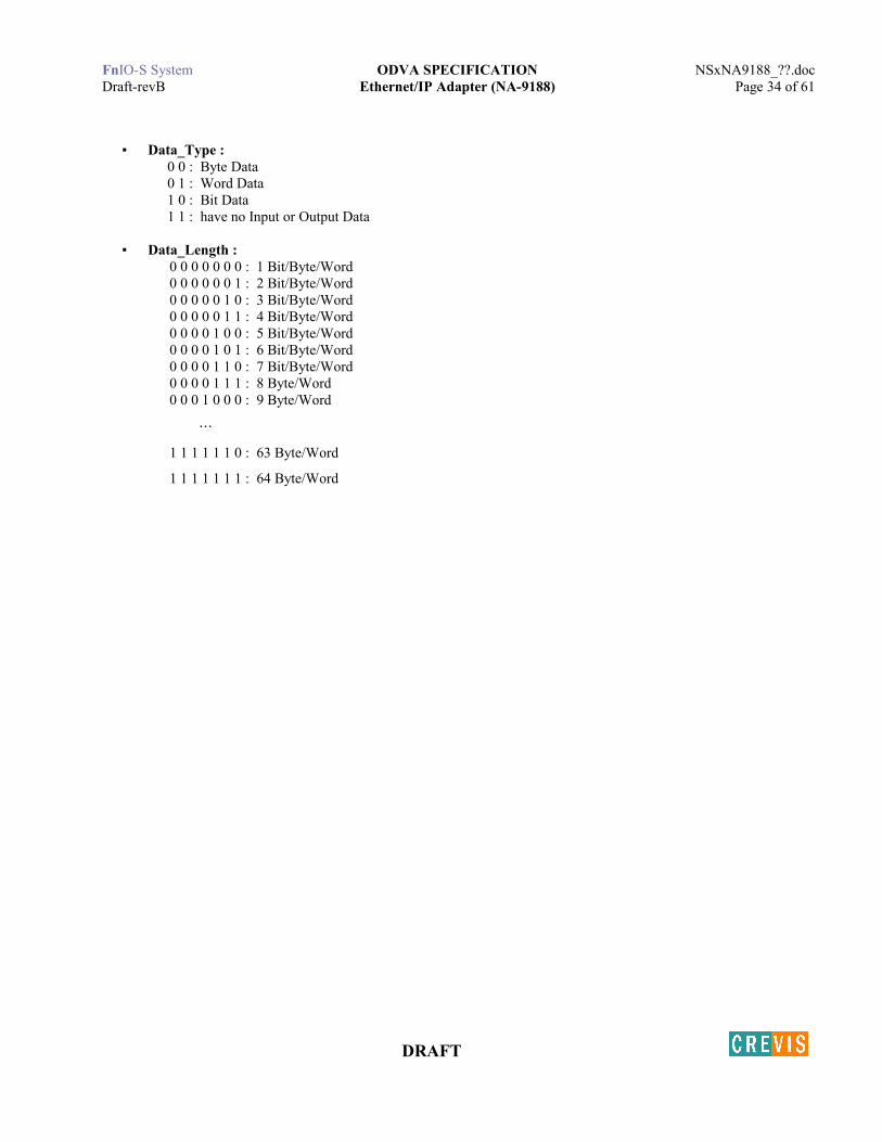
▪ Data_Type :0 0 : Byte Data0 1 : Word Data1 0 : Bit Data1 1 : have no Input or Output Data
▪ Data_Length :0 0 0 0 0 0 0 : 1 Bit/Byte/Word0 0 0 0 0 0 1 : 2 Bit/Byte/Word0 0 0 0 0 1 0 : 3 Bit/Byte/Word0 0 0 0 0 1 1 : 4 Bit/Byte/Word0 0 0 0 1 0 0 : 5 Bit/Byte/Word0 0 0 0 1 0 1 : 6 Bit/Byte/Word0 0 0 0 1 1 0 : 7 Bit/Byte/Word0 0 0 0 1 1 1 : 8 Byte/Word0 0 0 1 0 0 0 : 9 Byte/Word
…
1 1 1 1 1 1 0 : 63 Byte/Word
1 1 1 1 1 1 1 : 64 Byte/Word
DRAFT

FnIO-S System ODVA SPECIFICATION NSxNA9188_??.docDraft-revB Ethernet/IP Adapter (NA-9188) Page 35 of 61
3.11. Ethernet/IP Reference
Ethernet/IP Reference Documentshttp://www.odva.org http://www.ethernet-ip.org
Ethernet/IP Toolshttp://www.pyramid-solutions.com
DRAFT

FnIO-S System ODVA SPECIFICATION NSxNA9188_??.docDraft-revB Ethernet/IP Adapter (NA-9188) Page 36 of 61
APPENDIX A
A.1. Product List
No. ST-Number Description Module Id(hex)
Catalog Number Product Code
1 ST-1214 4-sinking input, 24Vdc 03 00 03 00 41 83 C0 40 012 ST-1224 4-sourcing input, 24Vdc 04 00 04 00 41 83 C0 40 013 ST-1218 8-sinking input, 24Vdc 07 00 07 00 41 00 C0 40 014 ST-1228 8-sourcing input, 24Vdc 08 00 08 00 41 00 C0 40 015 ST-121F 16-sinking input, 24Vdc 13 00 13 01 41 01 C0 40 016 ST-122F 16-sourcing input, 24Vdc 14 00 14 01 41 01 C0 40 017 ST-1314 4-sinking input, 48Vdc 05 00 05 00 41 83 C0 40 018 ST-1324 4-sourcing input, 48Vdc 06 00 06 00 41 83 C0 40 019 ST-1804 4-ac input, 110Vac 09 00 09 00 41 83 C0 40 0110 ST-1904 4-ac input, 220Vac 0A 00 0A 00 41 83 C0 40 0111 ST-2314 4-sinking output, 24Vdc 0.5A 0E 00 0E 00 81 C0 83 80 0112 ST-2324 4-sourcing output, 24Vdc 0.5A 10 00 10 00 81 C0 83 80 0113 ST-2318 8-sinking output, 24Vdc 0.5A 11 00 11 00 81 C0 00 80 0114 ST-2328 8-sourcing output, 24Vdc 0.5A 12 00 12 00 81 C0 00 80 0115 ST-221F 16-sinking output, 24Vdc 0.3A 15 00 15 01 81 C0 01 80 0116 ST-222F 16-sourcing output, 24Vdc 0.3A 16 00 16 01 81 C0 01 80 0117 ST-2414 4-sinking output, diag, 24Vdc 0.5A 37 37 00 00 C1 83 83 C0 0118 ST-2424 4-sourcing output, diag, 24Vdc 0.5A 38 38 00 00 C1 83 83 C0 0119 ST-2514 4-sinking output, diag, 24Vdc 2A 35 35 00 00 C1 83 83 C0 0120 ST-2524 4-sourcing output, diag, 24Vdc 2A 36 36 00 00 C1 83 83 C0 0121 ST-2742 2-relay output, 230Vac 2A 0B 00 0B 00 81 C0 81 80 0122 ST-2852 2-triac output, 120Vac 0.5A 0C 00 0C 00 81 C0 81 80 0123 ST-3114 4-current analog input, 0~20mA, 12bit 1C 00 1C 43 41 43 C0 60 0324 ST-3134 4-current analog input, 0~20mA, 14bit 1E 00 1E 43 41 43 C0 60 0325 ST-3214 4-current analog input, 4~20mA, 12bit 1D 00 1D 43 41 43 C0 68 0326 ST-3234 4-current analog input, 4~20mA, 14bit 1F 00 1F 43 41 43 C0 68 0327 ST-3424 4-voltage analog input, 0~10V, 12bit 20 00 20 43 41 43 C0 60 0328 ST-3444 4-voltage analog input, 0~10V, 14bit 22 00 22 43 41 43 C0 60 0329 ST-3524 4-voltage analog input, -10~10V, 12bit 21 00 21 43 41 43 C0 60 0330 ST-3544 4-voltage analog input, -10~10V, 14bit 23 00 23 43 41 43 C0 60 0331 ST-3624 4-voltage analog input, 0~5V, 12bit 24 00 24 43 41 43 C0 60 0332 ST-3644 4-voltage analog input, 0~5V, 14bit 25 00 25 43 41 43 C0 60 0333 ST-3702 2-RTD/Resistance input 28 00 28 41 41 41 C0 68 0334 ST-3802 2-Thermocouple/mV input 2A 00 2A 41 41 41 C0 68 0335 ST-4112 2-current analog output, 0~20mA, 12bit 2C 00 2C 41 81 C0 41 A0 0336 ST-4212 2-current analog output, 4~20mA, 12bit 2D 00 2D 41 81 C0 41 A0 0337 ST-4422 2-voltage analog output, 0~10Vdc, 12bit 2E 00 2E 41 81 C0 41 A0 0338 ST-4522 2-voltage analog output, -10~10Vdc, 12bit 2F 00 2F 41 81 C0 41 A0 0339 ST-4622 2-voltage analog output, 0~5Vdc, 12bit 30 00 30 41 81 C0 41 A0 0340 ST-5101 1 Channel, High Speed Counter, 5Vdc 34 34 05 01 C1 05 01 D0 0341 ST-5111 1 Channel, High Speed Counter, 24Vdc 39 39 05 01 C1 05 01 D0 0342 ST-5241 2-Axes Motion Controller * 41 41 07 07 C1 07 07 D0 01
DRAFT

FnIO-S System ODVA SPECIFICATION NSxNA9188_??.docDraft-revB Ethernet/IP Adapter (NA-9188) Page 37 of 61
43 1-channel RS232 Communication **44 2-channel RS232 Communication **45 1-channel RS422 Communication **46 1-channel RS485 Communication **47 2-channel RS485 Communication **48 4-input, 5Vdc **49 4-output, 5Vdc 20mA **
* Under development.** Under planning.
DRAFT
FnIO-S System ODVA SPECIFICATION NSxNA9188_??.docDraft-revB Ethernet/IP Adapter (NA-9188) Page 38 of 61
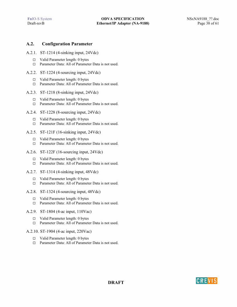
A.2. Configuration Parameter
A.2.1. ST-1214 (4-sinking input, 24Vdc) Valid Parameter length: 0 bytes Parameter Data: All of Parameter Data is not used.
A.2.2. ST-1224 (4-sourcing input, 24Vdc) Valid Parameter length: 0 bytes Parameter Data: All of Parameter Data is not used.
A.2.3. ST-1218 (8-sinking input, 24Vdc) Valid Parameter length: 0 bytes Parameter Data: All of Parameter Data is not used.
A.2.4. ST-1228 (8-sourcing input, 24Vdc) Valid Parameter length: 0 bytes Parameter Data: All of Parameter Data is not used.
A.2.5. ST-121F (16-sinking input, 24Vdc) Valid Parameter length: 0 bytes Parameter Data: All of Parameter Data is not used.
A.2.6. ST-122F (16-sourcing input, 24Vdc) Valid Parameter length: 0 bytes Parameter Data: All of Parameter Data is not used.
A.2.7. ST-1314 (4-sinking input, 48Vdc) Valid Parameter length: 0 bytes Parameter Data: All of Parameter Data is not used.
A.2.8. ST-1324 (4-sourcing input, 48Vdc) Valid Parameter length: 0 bytes Parameter Data: All of Parameter Data is not used.
A.2.9. ST-1804 (4-ac input, 110Vac) Valid Parameter length: 0 bytes Parameter Data: All of Parameter Data is not used.
A.2.10. ST-1904 (4-ac input, 220Vac) Valid Parameter length: 0 bytes Parameter Data: All of Parameter Data is not used.
DRAFT
FnIO-S System ODVA SPECIFICATION NSxNA9188_??.docDraft-revB Ethernet/IP Adapter (NA-9188) Page 39 of 61
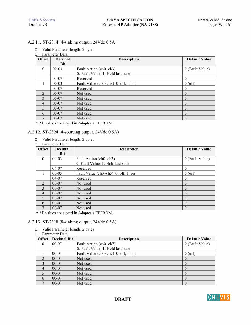
A.2.11. ST-2314 (4-sinking output, 24Vdc 0.5A) Valid Parameter length: 2 bytes Parameter Data:
Offset Decimal Bit
Description Default Value
0 00-03 Fault Action (ch0~ch3)0: Fault Value, 1: Hold last state
0 (Fault Value)
04-07 Reserved 01 00-03 Fault Value (ch0~ch3) 0: off, 1: on 0 (off)
04-07 Reserved 02 00-07 Not used 03 00-07 Not used 04 00-07 Not used 05 00-07 Not used 06 00-07 Not used 07 00-07 Not used 0
* All values are stored in Adapter’s EEPROM.
A.2.12. ST-2324 (4-sourcing output, 24Vdc 0.5A) Valid Parameter length: 2 bytes Parameter Data:
Offset Decimal Bit
Description Default Value
0 00-03 Fault Action (ch0~ch3)0: Fault Value, 1: Hold last state
0 (Fault Value)
04-07 Reserved 01 00-03 Fault Value (ch0~ch3) 0: off, 1: on 0 (off)
04-07 Reserved 02 00-07 Not used 03 00-07 Not used 04 00-07 Not used 05 00-07 Not used 06 00-07 Not used 07 00-07 Not used 0
* All values are stored in Adapter’s EEPROM.
A.2.13. ST-2318 (8-sinking output, 24Vdc 0.5A) Valid Parameter length: 2 bytes Parameter Data:
Offset Decimal Bit Description Default Value0 00-07 Fault Action (ch0~ch7)
0: Fault Value, 1: Hold last state0 (Fault Value)
1 00-07 Fault Value (ch0~ch7) 0: off, 1: on 0 (off)2 00-07 Not used 03 00-07 Not used 04 00-07 Not used 05 00-07 Not used 06 00-07 Not used 07 00-07 Not used 0
DRAFT

FnIO-S System ODVA SPECIFICATION NSxNA9188_??.docDraft-revB Ethernet/IP Adapter (NA-9188) Page 40 of 61
* All values are stored in Adapter’s EEPROM.
DRAFT
FnIO-S System ODVA SPECIFICATION NSxNA9188_??.docDraft-revB Ethernet/IP Adapter (NA-9188) Page 41 of 61
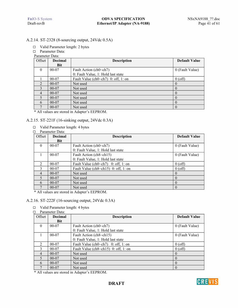
A.2.14. ST-2328 (8-sourcing output, 24Vdc 0.5A) Valid Parameter length: 2 bytes Parameter Data:Parameter Data:
Offset Decimal Bit
Description Default Value
0 00-07 Fault Action (ch0~ch7)0: Fault Value, 1: Hold last state
0 (Fault Value)
1 00-07 Fault Value (ch0~ch7) 0: off, 1: on 0 (off)2 00-07 Not used 03 00-07 Not used 04 00-07 Not used 05 00-07 Not used 06 00-07 Not used 07 00-07 Not used 0
* All values are stored in Adapter’s EEPROM.
A.2.15. ST-221F (16-sinking output, 24Vdc 0.3A) Valid Parameter length: 4 bytes Parameter Data:
Offset Decimal Bit
Description Default Value
0 00-07 Fault Action (ch0~ch7)0: Fault Value, 1: Hold last state
0 (Fault Value)
1 00-07 Fault Action (ch8~ch15)0: Fault Value, 1: Hold last state
0 (Fault Value)
2 00-07 Fault Value (ch0~ch7) 0: off, 1: on 0 (off)3 00-07 Fault Value (ch8~ch15) 0: off, 1: on 0 (off)4 00-07 Not used 05 00-07 Not used 06 00-07 Not used 07 00-07 Not used 0
* All values are stored in Adapter’s EEPROM.
A.2.16. ST-222F (16-sourcing output, 24Vdc 0.3A) Valid Parameter length: 4 bytes Parameter Data:
Offset Decimal Bit
Description Default Value
0 00-07 Fault Action (ch0~ch7)0: Fault Value, 1: Hold last state
0 (Fault Value)
1 00-07 Fault Action (ch8~ch15)0: Fault Value, 1: Hold last state
0 (Fault Value)
2 00-07 Fault Value (ch0~ch7) 0: off, 1: on 0 (off)3 00-07 Fault Value (ch8~ch15) 0: off, 1: on 0 (off)4 00-07 Not used 05 00-07 Not used 06 00-07 Not used 07 00-07 Not used 0
* All values are stored in Adapter’s EEPROM.
DRAFT

FnIO-S System ODVA SPECIFICATION NSxNA9188_??.docDraft-revB Ethernet/IP Adapter (NA-9188) Page 42 of 61
A.2.17. ST-2414 (4-sinking output, Diag, 24Vdc 0.5A) Valid Parameter length: 2 bytes Parameter Data:
Offset Decimal Bit
Description Default Value
0 00-03 Fault Action (ch0~ch3)0: Fault Value, 1: Hold last state
0 (Fault Value)
04-07 Reserved 01 00-03 Fault Value (ch0~ch3) 0: off, 1: on 0 (off)
04-07 Reserved 02 00-07 Not used 03 00-07 Not used 04 00-07 Not used 05 00-07 Not used 06 00-07 Not used 07 00-07 Not used 0
* All values are stored in Adapter’s EEPROM.
A.2.18. ST-2424 (4-sourcing output, Diag, 24Vdc 0.5A) Valid Parameter length: 2 bytes Parameter Data:
Offset Decimal Bit
Description Default Value
0 00-03 Fault Action (ch0~ch3)0: Fault Value, 1: Hold last state
0 (Fault Value)
04-07 Reserved 01 00-03 Fault Value (ch0~ch3) 0: off, 1: on 0 (off)
04-07 Reserved 02 00-07 Not used 03 00-07 Not used 04 00-07 Not used 05 00-07 Not used 06 00-07 Not used 07 00-07 Not used 0
* All values are stored in Adapter’s EEPROM.
A.2.19. ST-2514 (4-sinking output, Diag, 24Vdc 2A) Valid Parameter length: 2 bytes Parameter Data:
Offset Decimal Bit
Description Default Value
0 00-03 Fault Action (ch0~ch3)0: Fault Value, 1: Hold last state
0 (Fault Value)
04-07 Reserved 01 00-03 Fault Value (ch0~ch3) 0: off, 1: on 0 (off)
04-07 Reserved 02 00-07 Not used 03 00-07 Not used 04 00-07 Not used 0
DRAFT

FnIO-S System ODVA SPECIFICATION NSxNA9188_??.docDraft-revB Ethernet/IP Adapter (NA-9188) Page 43 of 61
5 00-07 Not used 06 00-07 Not used 07 00-07 Not used 0
* All values are stored in Adapter’s EEPROM.
A.2.20. ST-2524 (4-sourcing output, Diag, 24Vdc 2A) Valid Parameter length: 2 bytes Parameter Data:
Offset Decimal Bit
Description Default Value
0 00-03 Fault Action (ch0~ch3)0: Fault Value, 1: Hold last state
0 (Fault Value)
04-07 Reserved 01 00-03 Fault Value (ch0~ch3) 0: off, 1: on 0 (off)
04-07 Reserved 02 00-07 Not used 03 00-07 Not used 04 00-07 Not used 05 00-07 Not used 06 00-07 Not used 07 00-07 Not used 0
* All values are stored in Adapter’s EEPROM.
A.2.21. ST-2742 (2-relay output, 230Vac 2A) Valid Parameter length: 2 bytes Parameter Data:
Offset Decimal Bit
Description Default Value
0 00, 01 Fault Action (ch0, ch1)0: Fault Value, 1: Hold last state
0 (Fault Value)
02-07 Reserved 01 00, 01 Fault Value (ch0, ch1) 0: off, 1: on 0 (off)
02-07 Reserved 02 00-07 Not used 03 00-07 Not used 04 00-07 Not used 05 00-07 Not used 06 00-07 Not used 07 00-07 Not used 0
* All values are stored in Adapter’s EEPROM.
A.2.22. ST-2852 (2-triac output, 120Vac 0.5A) Valid Parameter length: 2 bytes Parameter Data:
Offset Decimal Bit
Description Default Value
0 00, 01 Fault Action (ch0, ch1)0: Fault Value, 1: Hold last state
0 (Fault Value)
02-07 Reserved 01 00, 01 Fault Value (ch0, ch1) 0: off, 1: on 0 (off)
DRAFT

FnIO-S System ODVA SPECIFICATION NSxNA9188_??.docDraft-revB Ethernet/IP Adapter (NA-9188) Page 44 of 61
02-07 Reserved 02 00-07 Not used 03 00-07 Not used 04 00-07 Not used 05 00-07 Not used 06 00-07 Not used 07 00-07 Not used 0
* All values are stored in Adapter’s EEPROM.
A.2.23. ST-3114 (4-current analog input, 0~20mA, 12bit) Valid Parameter length: 0 bytes Parameter Data: All of Parameter Data is not used.
A.2.24. ST-3134 (4-current analog input, 0~20mA, 14bit) Valid Parameter length: 0 bytes Parameter Data: All of Parameter Data is not used.
A.2.25. ST-3214 (4-current analog input, 4~20mA, 12bit) Valid Parameter length: 0 bytes Parameter Data: All of Parameter Data is not used.
A.2.26. ST-3234 (4-current analog input, 4~20mA, 14bit) Valid Parameter length: 0 bytes Parameter Data: All of Parameter Data is not used.
A.2.27. ST-3424 (4-voltage analog input, 0~10V, 12bit) Valid Parameter length: 0 bytes Parameter Data: All of Parameter Data is not used.
A.2.28. ST-3444 (4-voltage analog input, 0~10V, 14bit) Valid Parameter length: 0 bytes Parameter Data: All of Parameter Data is not used.
A.2.29. ST-3524 (4-voltage analog input, -10~10V, 12bit) Valid Parameter length: 0 bytes Parameter Data: All of Parameter Data is not used.
A.2.30. ST-3544 (4-voltage analog input, -10~10V, 14bit) Valid Parameter length: 0 bytes Parameter Data: All of Parameter Data is not used.
A.2.31. ST-3624 (4-voltage analog input, 0~5V, 12bit) Valid Parameter length: 0 bytes Parameter Data: All of Parameter Data is not used.
A.2.32. ST-3644 (4-voltage analog input, 0~5V, 14bit) Valid Parameter length: 0 bytes Parameter Data: All of Parameter Data is not used.
DRAFT

FnIO-S System ODVA SPECIFICATION NSxNA9188_??.docDraft-revB Ethernet/IP Adapter (NA-9188) Page 45 of 61
DRAFT

FnIO-S System ODVA SPECIFICATION NSxNA9188_??.docDraft-revB Ethernet/IP Adapter (NA-9188) Page 46 of 61
A.2.33. ST-3702 (2- RTD/Resistance input) Valid Parameter length: 2 bytes Parameter Data:
Offset Decimal Bit
Description Default Value
0 00-07 The selection Sensor Type=00h:PT100, 0.00385, -200~850°C, 0.1°C /count=01h:PT200, 0.00385, -200~850°C, 0.1°C/count=02h:PT500, 0.00385, -200~850°C, 0.1°C/count=03h:PT1000, 0.00385, -200~350°C, 0.1°C/count=04h:PT50, 0.00385, -200~850°C, 0.1°C/count=10h:JPT100, 0.003916, -200~640°C, 0.1°C/count =11h:JPT200, 0.003916, -200~640°C, 0.1°C/count=12h:JPT500, 0.003916, -200~640°C, 0.1°C/count=13h:JPT1000, 0.003916, -200~350°C, 0.1°C/count=20h:NI100, 0.00618, -60~250°C, 0.1°C/count=21h:NI200, 0.00618, -60~250°C, 0.1°C/count=22h:NI500, 0.00618, -60~250°C, 0.1°C/count=23h:NI1000, 0.00618, -60~180°C, 0.1°C/count=30h:NI120, 0.00672, -80~250°C, 0.1°C/count=40h:CU10, 0.00427, -200~260°C, 0.1°C/count=80h:Resistance Input, 1~2000Ω, 100mΩ /1count=81h: Resistance Input, 1~327Ω, 10mΩ/1count=82h: Resistance Input, 1~620Ω, 20mΩ/1count=Others: Reserved
0: PT100
1 00 Temperature Type0: Celsius(°C), 1: Fahrenheit(°F)
0: Celsius(°C)
01-03 Reserved 004 Filter Type
0: Normal Filter, 1: Enhanced Filter0: Normal Filter
05-07 Reserved 02 00-07 Not used 03 00-07 Not used 04 00-07 Not used 05 00-07 Not used 06 00-07 Not used 07 00-07 Not used 0
* All values are stored in Adapter’s EEPROM.
DRAFT

FnIO-S System ODVA SPECIFICATION NSxNA9188_??.docDraft-revB Ethernet/IP Adapter (NA-9188) Page 47 of 61
A.2.34. ST-3802 (2- Thermocouple/mV input) Valid Parameter length: 2 bytes Parameter Data:
Offset Decimal Bit
Description Default Value
0 00-07 The selection Sensor Type=00h: Type K, 0.1°C/count=01h: Type J, 0.1°C/count=02h: Type T, 0.1°C/count=03h: Type B, 0.1°C/count=04h: Type R, 0.1°C/count=05h: Type S, 0.1°C/count=06h: Type E, 0.1°C/count=07h: Type N, 0.1°C/count=08h: Type L, 0.1°C/count=09h: Type U, 0.1°C/count=0Ah: Type C, 0.1°C/count=0Bh: Type D, 0.1°C/count=80h: 10uV Input, -78.0~78.0mV, 10uV/count=81h: 1uV Input, -32.7~32.7mV, 1uV/count=82h: 2uV Input, -65.5~65.5mV, 2uV/count=Others: Reserved
0: Type K
1 00 Temperature Type0: Celsius(°C), 1: Fahrenheit(°F)
0: Celsius(°C)
01 0: Cold Junction Compensation1: Disable Compensation
0
02, 03 Reserved 004 Filter Type
0: Normal Filter, 1: Enhanced Filter0: Normal Filter
05-07 Reserved 02 00-07 Not used 03 00-07 Not used 04 00-07 Not used 05 00-07 Not used 06 00-07 Not used 07 00-07 Not used 0
* All values are stored in Adapter’s EEPROM.
DRAFT
FnIO-S System ODVA SPECIFICATION NSxNA9188_??.docDraft-revB Ethernet/IP Adapter (NA-9188) Page 48 of 61
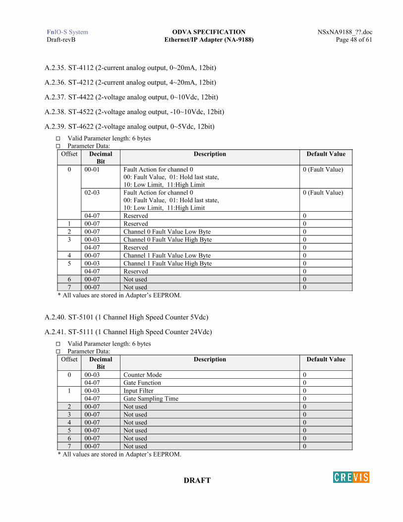
A.2.35. ST-4112 (2-current analog output, 0~20mA, 12bit)
A.2.36. ST-4212 (2-current analog output, 4~20mA, 12bit)
A.2.37. ST-4422 (2-voltage analog output, 0~10Vdc, 12bit)
A.2.38. ST-4522 (2-voltage analog output, -10~10Vdc, 12bit)
A.2.39. ST-4622 (2-voltage analog output, 0~5Vdc, 12bit) Valid Parameter length: 6 bytes Parameter Data:
Offset Decimal Bit
Description Default Value
0 00-01 Fault Action for channel 000: Fault Value, 01: Hold last state, 10: Low Limit, 11:High Limit
0 (Fault Value)
02-03 Fault Action for channel 000: Fault Value, 01: Hold last state, 10: Low Limit, 11:High Limit
0 (Fault Value)
04-07 Reserved 01 00-07 Reserved 02 00-07 Channel 0 Fault Value Low Byte 03 00-03 Channel 0 Fault Value High Byte 0
04-07 Reserved 04 00-07 Channel 1 Fault Value Low Byte 05 00-03 Channel 1 Fault Value High Byte 0
04-07 Reserved 06 00-07 Not used 07 00-07 Not used 0
* All values are stored in Adapter’s EEPROM.
A.2.40. ST-5101 (1 Channel High Speed Counter 5Vdc)
A.2.41. ST-5111 (1 Channel High Speed Counter 24Vdc) Valid Parameter length: 6 bytes Parameter Data:
Offset Decimal Bit
Description Default Value
0 00-03 Counter Mode 004-07 Gate Function 0
1 00-03 Input Filter 004-07 Gate Sampling Time 0
2 00-07 Not used 03 00-07 Not used 04 00-07 Not used 05 00-07 Not used 06 00-07 Not used 07 00-07 Not used 0
* All values are stored in Adapter’s EEPROM.
DRAFT
FnIO-S System ODVA SPECIFICATION NSxNA9188_??.docDraft-revB Ethernet/IP Adapter (NA-9188) Page 49 of 61
A.3. Memory Register
A.3.1. ST-1214 (4-sinking input, 24Vdc) Memory Register length: 0 bytes Memory Register: none
A.3.2. ST-1224 (4-sourcing input, 24Vdc) Memory Register length: 0 bytes Memory Register: none
A.3.3. ST-1218 (8-sinking input, 24Vdc) Memory Register length: 0 bytes Memory Register: none
A.3.4. ST-1228 (8-sourcing input, 24Vdc) Memory Register length: 0 bytes Memory Register: none
A.3.5. ST-121F (16-sinking input, 24Vdc) Memory Register length: 0 bytes Memory Register: none
A.3.6. ST-122F (16-sourcing input, 24Vdc) Memory Register length: 0 bytes Memory Register: none
A.3.7. ST-1314 (4-sinking input, 48Vdc) Memory Register length: 0 bytes Memory Register: none
A.3.8. ST-1324 (4-sourcing input, 48Vdc) Memory Register length: 0 bytes Memory Register: none
A.3.9. ST-1804 (4-ac input, 110Vac) Memory Register length: 0 bytes Memory Register: none
A.3.10. ST-1904 (4-ac input, 220Vac) Memory Register length: 0 bytes Memory Register: none
A.3.11. ST-2314 (4-sinking output, 24Vdc 0.5A) Memory Register length: 0 bytes Memory Register: none
DRAFT

FnIO-S System ODVA SPECIFICATION NSxNA9188_??.docDraft-revB Ethernet/IP Adapter (NA-9188) Page 50 of 61
A.3.12. ST-2324 (4-sourcing output, 24Vdc 0.5A) Memory Register length: 0 bytes Memory Register: none
A.3.13. ST-2318 (8-sinking output, 24Vdc 0.5A) Memory Register length: 0 bytes Memory Register: none
A.3.14. ST-2328 (8-sourcing output, 24Vdc 0.5A) Memory Register length: 0 bytes Memory Register: none
A.3.15. ST-221F (16-sinking output, 24Vdc 0.1A) Memory Register length: 0 bytes Memory Register: none
A.3.16. ST-222F (16-sourcing output, 24Vdc 0.1A) Memory Register length: 0 bytes Memory Register: none
A.3.17. ST-2414 (4-sinking output, Diag, 24Vdc 0.5A) Memory Register length: 0 bytes Memory Register: none
A.3.18. ST-2424 (4-sourcing output, Diag, 24Vdc 0.5A) Memory Register length: 0 bytes Memory Register: none
A.3.19. ST-2514 (4-sinking output, Diag, 24Vdc 2A) Memory Register length: 0 bytes Memory Register: none
A.3.20. ST-2524 (4-sourcing output, Diag, 24Vdc 2A) Memory Register length: 0 bytes Memory Register: none
A.3.21. ST-2742 (2-relay output, 230Vac 2A) Memory Register length: 0 bytes Memory Register: none
A.3.22. ST-2852 (2-triac output, 120Vac 0.5A) Memory Register length: 0 bytes Memory Register: none
DRAFT

FnIO-S System ODVA SPECIFICATION NSxNA9188_??.docDraft-revB Ethernet/IP Adapter (NA-9188) Page 51 of 61
A.3.23. ST-3114 (4-current analog input, 0~20mA, 12bit) Memory Register length: 10 bytes Memory Register:
Offset Access Decimal Bit
Description Default Value
0 R 00-07 Channel 0 Input Data Low 8 bits1 R 00-03 Channel 0 Input Data High 4 bits
04-07 not used 02 R 00-07 Channel 1 Input Data Low 8 bits3 R 00-03 Channel 1 Input Data High 4 bits
04-07 not used 04 R 00-07 Channel 2 Input Data Low 8 bits5 R 00-03 Channel 2 Input Data High 4 bits
04-07 not used 06 R 00-07 Channel 3 Input Data Low 8 bits7 R 00-03 Channel 3 Input Data High 4 bits
04-07 not used 08 R 00-07 Reserved 09 R 00-07 Reserved 0
A.3.24. ST-3134 (4-current analog input, 0~20mA, 14bit) Memory Register length: 10 bytes Memory Register:
Offset Access Decimal Bit
Description Default Value
0 R 00-07 Channel 0 Input Data Low 8 bits1 R 00-05 Channel 0 Input Data High 6 bits
06, 07 not used 02 R 00-07 Channel 1 Input Data Low 8 bits3 R 00-05 Channel 1 Input Data High 6 bits
06, 07 not used 04 R 00-07 Channel 2 Input Data Low 8 bits5 R 00-05 Channel 2 Input Data High 6 bits
06, 07 not used 06 R 00-07 Channel 3 Input Data Low 8 bits7 R 00-05 Channel 3 Input Data High 6 bits
06, 07 not used 08 R 00-07 Reserved 09 R 00-07 Reserved 0
DRAFT

FnIO-S System ODVA SPECIFICATION NSxNA9188_??.docDraft-revB Ethernet/IP Adapter (NA-9188) Page 52 of 61
A.3.25. ST-3214 (4-current analog input, 4~20mA, 12bit) Memory Register length: 10 bytes Memory Register:
Offset Access Decimal Bit
Description Default Value
0 R 00-07 Channel 0 Input Data Low 8 bits1 R 00-03 Channel 0 Input Data High 4 bits
04-07 not used 02 R 00-07 Channel 1 Input Data Low 8 bits3 R 00-03 Channel 1 Input Data High 4 bits
04-07 not used 04 R 00-07 Channel 2 Input Data Low 8 bits5 R 00-03 Channel 2 Input Data High 4 bits
04-07 not used 06 R 00-07 Channel 3 Input Data Low 8 bits7 R 00-03 Channel 3 Input Data High 4 bits
04-07 not used 08 R 00-03 Alarm Status Bit for individual channels - Bit 00 corresponds to
input channel 0, bit 01 corresponds to input channel 1, and so on.When set(1), the input signal is below the input channel’s minimum range(3mA). And Input Data will be 0x8000(-32678)
04-07 Reserved 09 R 00-07 Reserved 0
A.3.26. ST-3234 (4-current analog input, 4~20mA, 14bit) Memory Register length: 10 bytes Memory Register:
Offset Access Decimal Bit
Description Default Value
0 R 00-07 Channel 0 Input Data Low 8 bits1 R 00-05 Channel 0 Input Data High 6 bits
06, 07 not used 02 R 00-07 Channel 1 Input Data Low 8 bits3 R 00-05 Channel 1 Input Data High 6 bits
06, 07 not used 04 R 00-07 Channel 2 Input Data Low 8 bits5 R 00-05 Channel 2 Input Data High 6 bits
06, 07 not used 06 R 00-07 Channel 3 Input Data Low 8 bits7 R 00-05 Channel 3 Input Data High 6 bits
06, 07 not used 08 R 00-03 Alarm Status Bit for individual channels - Bit 00 corresponds to
input channel 0, bit 01 corresponds to input channel 1, and so on.When set(1), the input signal is below the input channel’s minimum range(3mA). And Input Data will be 0x8000(-32678)
04-07 Reserved 09 R 00-07 Reserved 0
DRAFT

FnIO-S System ODVA SPECIFICATION NSxNA9188_??.docDraft-revB Ethernet/IP Adapter (NA-9188) Page 53 of 61
A.3.27. ST-3424 (4-voltage analog input, 0~10V, 12bit) Memory Register length: 10 bytes Memory Register:
Offset Access Decimal Bit
Description Default Value
0 R 00-07 Channel 0 Input Data Low 8 bits1 R 00-03 Channel 0 Input Data High 4 bits
04-07 not used 02 R 00-07 Channel 1 Input Data Low 8 bits3 R 00-03 Channel 1 Input Data High 4 bits
04-07 not used 04 R 00-07 Channel 2 Input Data Low 8 bits5 R 00-03 Channel 2 Input Data High 4 bits
04-07 not used 06 R 00-07 Channel 3 Input Data Low 8 bits7 R 00-03 Channel 3 Input Data High 4 bits
04-07 not used 08 R 00-07 Reserved 09 R 00-07 Reserved 0
A.3.28. ST-3444 (4-voltage analog input, 0~10V, 14bit) Memory Register length: 10 bytes Memory Register:
Offset Access Decimal Bit
Description Default Value
0 R 00-07 Channel 0 Input Data Low 8 bits1 R 00-05 Channel 0 Input Data High 6 bits
06, 07 not used 02 R 00-07 Channel 1 Input Data Low 8 bits3 R 00-05 Channel 1 Input Data High 6 bits
06, 07 not used 04 R 00-07 Channel 2 Input Data Low 8 bits5 R 00-05 Channel 2 Input Data High 6 bits
06, 07 not used 06 R 00-07 Channel 3 Input Data Low 8 bits7 R 00-05 Channel 3 Input Data High 6 bits
06, 07 not used 08 R 00-07 Reserved 09 R 00-07 Reserved 0
DRAFT
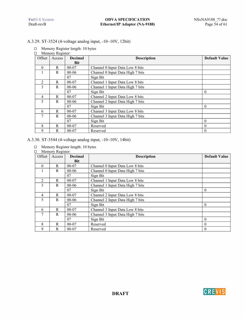
FnIO-S System ODVA SPECIFICATION NSxNA9188_??.docDraft-revB Ethernet/IP Adapter (NA-9188) Page 54 of 61
A.3.29. ST-3524 (4-voltage analog input, -10~10V, 12bit) Memory Register length: 10 bytes Memory Register:
Offset Access Decimal Bit
Description Default Value
0 R 00-07 Channel 0 Input Data Low 8 bits1 R 00-06 Channel 0 Input Data High 7 bits
07 Sign Bit2 R 00-07 Channel 1 Input Data Low 8 bits3 R 00-06 Channel 1 Input Data High 7 bits
07 Sign Bit 04 R 00-07 Channel 2 Input Data Low 8 bits5 R 00-06 Channel 2 Input Data High 7 bits
07 Sign Bit 06 R 00-07 Channel 3 Input Data Low 8 bits7 R 00-06 Channel 3 Input Data High 7 bits
07 Sign Bit 08 R 00-07 Reserved 09 R 00-07 Reserved 0
A.3.30. ST-3544 (4-voltage analog input, -10~10V, 14bit) Memory Register length: 10 bytes Memory Register:
Offset Access Decimal Bit
Description Default Value
0 R 00-07 Channel 0 Input Data Low 8 bits1 R 00-06 Channel 0 Input Data High 7 bits
07 Sign Bit2 R 00-07 Channel 1 Input Data Low 8 bits3 R 00-06 Channel 1 Input Data High 7 bits
07 Sign Bit 04 R 00-07 Channel 2 Input Data Low 8 bits5 R 00-06 Channel 2 Input Data High 7 bits
07 Sign Bit 06 R 00-07 Channel 3 Input Data Low 8 bits7 R 00-06 Channel 3 Input Data High 7 bits
07 Sign Bit 08 R 00-07 Reserved 09 R 00-07 Reserved 0
DRAFT

FnIO-S System ODVA SPECIFICATION NSxNA9188_??.docDraft-revB Ethernet/IP Adapter (NA-9188) Page 55 of 61
A.3.31. ST-3624 (4-voltage analog input, 0~5V, 12bit) Memory Register length: 10 bytes Memory Register:
Offset Access Decimal Bit
Description Default Value
0 R 00-07 Channel 0 Input Data Low 8 bits1 R 00-03 Channel 0 Input Data High 4 bits
04-07 not used 02 R 00-07 Channel 1 Input Data Low 8 bits3 R 00-03 Channel 1 Input Data High 4 bits
04-07 not used 04 R 00-07 Channel 2 Input Data Low 8 bits5 R 00-03 Channel 2 Input Data High 4 bits
04-07 not used 06 R 00-07 Channel 3 Input Data Low 8 bits7 R 00-03 Channel 3 Input Data High 4 bits
04-07 not used 08 R 00-07 Reserved 09 R 00-07 Reserved 0
A.3.32. ST-3644 (4-voltage analog input, 0~5V, 14bit) Memory Register length: 10 bytes Memory Register:
Offset Access Decimal Bit
Description Default Value
0 R 00-07 Channel 0 Input Data Low 8 bits1 R 00-05 Channel 0 Input Data High 6 bits
06, 07 not used 02 R 00-07 Channel 1 Input Data Low 8 bits3 R 00-05 Channel 1 Input Data High 6 bits
06, 07 not used 04 R 00-07 Channel 2 Input Data Low 8 bits5 R 00-05 Channel 2 Input Data High 6 bits
06, 07 not used 06 R 00-07 Channel 3 Input Data Low 8 bits7 R 00-05 Channel 3 Input Data High 6 bits
06, 07 not used 08 R 00-07 Reserved 09 R 00-07 Reserved 0
DRAFT
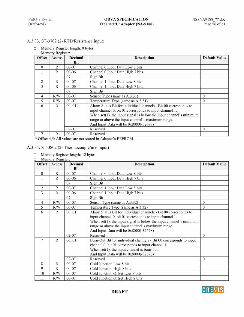
FnIO-S System ODVA SPECIFICATION NSxNA9188_??.docDraft-revB Ethernet/IP Adapter (NA-9188) Page 56 of 61
A.3.33. ST-3702 (2- RTD/Resistance input) Memory Register length: 8 bytes Memory Register:
Offset Access Decimal Bit
Description Default Value
0 R 00-07 Channel 0 Input Data Low 8 bits1 R 00-06 Channel 0 Input Data High 7 bits
07 Sign Bit2 R 00-07 Channel 1 Input Data Low 8 bits3 R 00-06 Channel 1 Input Data High 7 bits
07 Sign Bit4 R/W 00-07 Sensor Type (same as A.3.31) 05 R/W 00-07 Temperature Type (same as A.3.31) 06 R 00, 01 Alarm Status Bit for individual channels - Bit 00 corresponds to
input channel 0, bit 01 corresponds to input channel 1.When set(1), the input signal is below the input channel’s minimum range or above the input channel’s maximum range.And Input Data will be 0x8000(-32678)
02-07 Reserved 07 R 00-07 Reserved
* Offset 4,5: All values are not stored in Adapter’s EEPROM.
A.3.34. ST-3802 (2- Thermocouple/mV input) Memory Register length: 12 bytes Memory Register:
Offset Access Decimal Bit
Description Default Value
0 R 00-07 Channel 0 Input Data Low 8 bits1 R 00-06 Channel 0 Input Data High 7 bits
07 Sign Bit2 R 00-07 Channel 1 Input Data Low 8 bits3 R 00-06 Channel 1 Input Data High 7 bits
07 Sign Bit4 R/W 00-07 Sensor Type (same as A.3.32) 05 R/W 00-07 Temperature Type (same as A.3.32) 06 R 00, 01 Alarm Status Bit for individual channels - Bit 00 corresponds to
input channel 0, bit 01 corresponds to input channel 1.When set(1), the input signal is below the input channel’s minimum range or above the input channel’s maximum range.And Input Data will be 0x8000(-32678)
02-07 Reserved 07 R 00, 01 Burn-Out Bit for individual channels - Bit 00 corresponds to input
channel 0, bit 01 corresponds to input channel 1.When set(1), the input channel is burn-out.And Input Data will be 0x8000(-32678)
02-07 Reserved 08 R 00-07 Cold Junction Low 8 bits9 R 00-07 Cold Junction High 8 bits10 R/W 00-07 Cold Junction Offset Low 8 bits11 R/W 00-07 Cold Junction Offset High 8 bits
DRAFT

FnIO-S System ODVA SPECIFICATION NSxNA9188_??.docDraft-revB Ethernet/IP Adapter (NA-9188) Page 57 of 61
* Offset 4,5,10,11: All values are not stored in Adapter’s EEPROM.
DRAFT
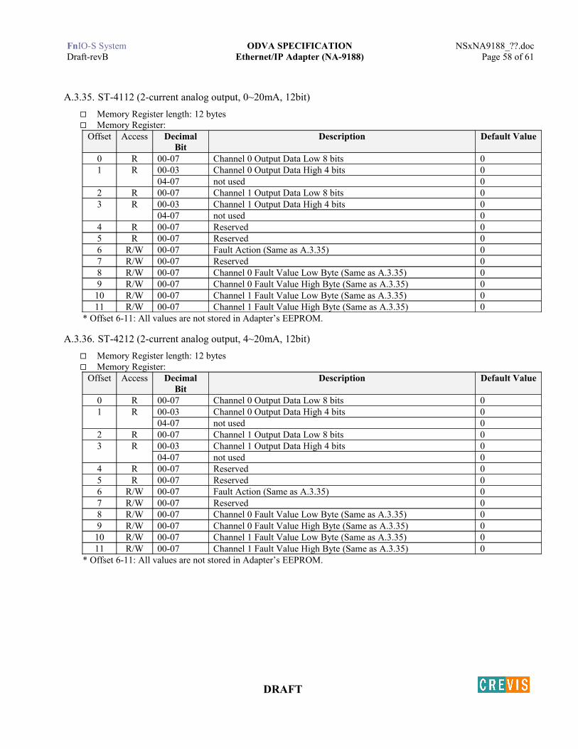
FnIO-S System ODVA SPECIFICATION NSxNA9188_??.docDraft-revB Ethernet/IP Adapter (NA-9188) Page 58 of 61
A.3.35. ST-4112 (2-current analog output, 0~20mA, 12bit) Memory Register length: 12 bytes Memory Register:
Offset Access Decimal Bit
Description Default Value
0 R 00-07 Channel 0 Output Data Low 8 bits 01 R 00-03 Channel 0 Output Data High 4 bits 0
04-07 not used 02 R 00-07 Channel 1 Output Data Low 8 bits 03 R 00-03 Channel 1 Output Data High 4 bits 0
04-07 not used 04 R 00-07 Reserved 05 R 00-07 Reserved 06 R/W 00-07 Fault Action (Same as A.3.35) 07 R/W 00-07 Reserved 08 R/W 00-07 Channel 0 Fault Value Low Byte (Same as A.3.35) 09 R/W 00-07 Channel 0 Fault Value High Byte (Same as A.3.35) 010 R/W 00-07 Channel 1 Fault Value Low Byte (Same as A.3.35) 011 R/W 00-07 Channel 1 Fault Value High Byte (Same as A.3.35) 0
* Offset 6-11: All values are not stored in Adapter’s EEPROM.
A.3.36. ST-4212 (2-current analog output, 4~20mA, 12bit) Memory Register length: 12 bytes Memory Register:
Offset Access Decimal Bit
Description Default Value
0 R 00-07 Channel 0 Output Data Low 8 bits 01 R 00-03 Channel 0 Output Data High 4 bits 0
04-07 not used 02 R 00-07 Channel 1 Output Data Low 8 bits 03 R 00-03 Channel 1 Output Data High 4 bits 0
04-07 not used 04 R 00-07 Reserved 05 R 00-07 Reserved 06 R/W 00-07 Fault Action (Same as A.3.35) 07 R/W 00-07 Reserved 08 R/W 00-07 Channel 0 Fault Value Low Byte (Same as A.3.35) 09 R/W 00-07 Channel 0 Fault Value High Byte (Same as A.3.35) 010 R/W 00-07 Channel 1 Fault Value Low Byte (Same as A.3.35) 011 R/W 00-07 Channel 1 Fault Value High Byte (Same as A.3.35) 0
* Offset 6-11: All values are not stored in Adapter’s EEPROM.
DRAFT

FnIO-S System ODVA SPECIFICATION NSxNA9188_??.docDraft-revB Ethernet/IP Adapter (NA-9188) Page 59 of 61
A.3.37. ST-4422 (2-voltage analog output, 0~10Vdc, 12bit) Memory Register length: 12 bytes Memory Register:
Offset Access Decimal Bit
Description Default Value
0 R 00-07 Channel 0 Output Data Low 8 bits 01 R 00-03 Channel 0 Output Data High 4 bits 0
04-07 not used 02 R 00-07 Channel 1 Output Data Low 8 bits 03 R 00-03 Channel 1 Output Data High 4 bits 0
04-07 not used 04 R 00-07 Reserved 05 R 00-07 Reserved 06 R/W 00-07 Fault Action (Same as A.3.35) 07 R/W 00-07 Reserved 08 R/W 00-07 Channel 0 Fault Value Low Byte (Same as A.3.35) 09 R/W 00-07 Channel 0 Fault Value High Byte (Same as A.3.35) 010 R/W 00-07 Channel 1 Fault Value Low Byte (Same as A.3.35) 011 R/W 00-07 Channel 1 Fault Value High Byte (Same as A.3.35) 0
* Offset 6-11: All values are not stored in Adapter’s EEPROM.
A.3.38. ST-4522 (2-voltage analog output, -10~10Vdc, 12bit) Memory Register length: 12 bytes Memory Register:
Offset Access Decimal Bit
Description Default Value
0 R 00-07 Channel 0 Output Data Low 8 bits 01 R 00-03 Channel 0 Output Data High 4 bits 0
04-07 not used 02 R 00-07 Channel 1 Output Data Low 8 bits 03 R 00-03 Channel 1 Output Data High 4 bits 0
04-07 not used 04 R 00-07 Reserved 05 R 00-07 Reserved 06 R/W 00-07 Fault Action (Same as A.3.35) 07 R/W 00-07 Reserved 08 R/W 00-07 Channel 0 Fault Value Low Byte (Same as A.3.35) 09 R/W 00-07 Channel 0 Fault Value High Byte (Same as A.3.35) 010 R/W 00-07 Channel 1 Fault Value Low Byte (Same as A.3.35) 011 R/W 00-07 Channel 1 Fault Value High Byte (Same as A.3.35) 0
* Offset 6-11: All values are not stored in Adapter’s EEPROM.
DRAFT

FnIO-S System ODVA SPECIFICATION NSxNA9188_??.docDraft-revB Ethernet/IP Adapter (NA-9188) Page 60 of 61
A.3.39. ST-4622 (2-voltage analog output, 0~5Vdc, 12bit) Memory Register length: 12 bytes Memory Register:
Offset Access Decimal Bit
Description Default Value
0 R 00-07 Channel 0 Output Data Low 8 bits 01 R 00-03 Channel 0 Output Data High 4 bits 0
04-07 not used 02 R 00-07 Channel 1 Output Data Low 8 bits 03 R 00-03 Channel 1 Output Data High 4 bits 0
04-07 not used 04 R 00-07 Reserved 05 R 00-07 Reserved 06 R/W 00-07 Fault Action (Same as A.3.35) 07 R/W 00-07 Reserved 08 R/W 00-07 Channel 0 Fault Value Low Byte (Same as A.3.35) 09 R/W 00-07 Channel 0 Fault Value High Byte (Same as A.3.35) 010 R/W 00-07 Channel 1 Fault Value Low Byte (Same as A.3.35) 011 R/W 00-07 Channel 1 Fault Value High Byte (Same as A.3.35) 0
* Offset 6-11: All values are not stored in Adapter’s EEPROM.
A.3.40. ST-5101 (1 Channel High Speed Counter 5Vdc)
A.3.41. ST-5111 (1 Channel High Speed Counter 24Vdc) Memory Register length: 24 bytes Memory Register:
Offset Access Decimal Bit
Description Default Value
0 R 00-07 Current count value Low byte 01 R 00-07 Current count value Middle byte 02 R 00-07 Current count value High byte 03 R 00-07 Always 0 04 R 00-07 Status Low (compared flags) 05 R 00-07 Status High (same as LED display) 06 R 00-07 Output Terminal (OT) Control 07 R 00-07 SSR(Special Selection Register) 08 R/W 00-07 Gate Function/Counter Mode (Same as A.3.36) 09 R/W 00-07 Gate Sampling Time/Input Filter (Same as A.3.36) 010 R/W 00-07 Don’t care 011 R/W 00-07 Don’t care 012 R 00-07 Stored count value Low byte 013 R 00-07 Stored count value Middle byte 014 R 00-07 Stored count value High byte 015 R 00-07 Always 0 016 R/W 00-07 Initial Counter Value Low byte
(Initial counter or PWM Frequency value)0
17 R/W 00-07 Initial Counter Value Middle byte(Initial counter or PWM Frequency value)
0
DRAFT

FnIO-S System ODVA SPECIFICATION NSxNA9188_??.docDraft-revB Ethernet/IP Adapter (NA-9188) Page 61 of 61
18 R/W 00-07 Initial count value High byte(Initial counter or PWM Frequency value)
0
19 R/W 00-07 Always 0 020 R/W 00-07 Compare count value Low byte 021 R/W 00-07 Compare count value Middle byte 022 R/W 00-07 Compare count value High byte 023 R/W 00-07 Always 0 0
* Offset 8-9: All values are not stored in Adapter’s EEPROM.
DRAFT