Embed Size (px)
Citation preview

RSC Advances
PAPER
Ope
n A
cces
s A
rtic
le. P
ublis
hed
on 2
8 Se
ptem
ber
2018
. Dow
nloa
ded
on 1
/16/
2022
6:1
6:14
AM
. T
his
artic
le is
lice
nsed
und
er a
Cre
ativ
e C
omm
ons
Attr
ibut
ion-
Non
Com
mer
cial
3.0
Unp
orte
d L
icen
ce.
View Article OnlineView Journal | View Issue
Flexible Fe3Si/SiC
aScience and Technology on Thermostruc
Northwestern Polytechnical University, 71
nwpu.edu.cn; [email protected] Laboratories, National Universit
117411, SingaporecCollege of Material Science and Technolog
Astronautics, 210016, Nanjing, ChinadDepartment of Mechanical Engineering, K
United Arab Emirates
† Electronic supplementary informa10.1039/c8ra06941g
Cite this: RSC Adv., 2018, 8, 33574
Received 20th August 2018Accepted 23rd September 2018
DOI: 10.1039/c8ra06941g
rsc.li/rsc-advances
33574 | RSC Adv., 2018, 8, 33574–3358
ultrathin hybrid fiber mats withdesignable microwave absorption performance†
Yi Hou, a Yani Zhang,*a Xiaoqing Du,a Yong Yang,b Chaoran Deng,b Zhihong Yang,c
Lianxi Zheng d and Laifei Cheng*a
Flexible Fe3Si/SiC ultrathin fiber mats have been fabricated by electrospinning and high temperature
treatment (1400 �C) using polycarbosilane (PCS) and ferric acetylacetonate (Fe(acac)3) as precursors. The
crystallization degree, flexibility, electrical conductivity, dielectric loss and microwave absorption
properties of the hybrid fibers have been dramatically enhanced by the introduction of Fe. Fe3Si
nanoparticles with a diameter around 500 nm are embedded in SiC fibers. As the Fe3Si content increases
from 0 to 6.5 wt%, the related saturation magnetization (Ms) values increase from 0 to 8.4 emu g�1, and
the electrical conductivity rises from 7.9 � 10�8 to 3.1 � 10�3 S cm�1. Moreover, the flexibility of Fe3Si/
SiC hybrid fiber mats is greatly improved and remains intact after 500 times 180�-bending testing.
Compared with pure SiC fibers, the Fe3Si/SiC hybrid fibers process higher dielectric and magnetic loss,
which would be further advanced as more Fe3Si phase is introduced. At the optimal Fe3Si content of
3.8 wt%, the Fe3Si/SiC fibers/silicon resin composite (5 wt%) exhibits minimal reflection loss (RL) of �22.5
dB at 16.5 GHz and 2.5 mm thickness with a wide effective absorption bandwidth (EAB, RL < �10 dB) of
8.5 GHz. The microwave absorption performance can be further promoted by multi component stacking
fiber mat composites which contain both low and high Fe3Si content layers. Furthermore, the position of
the microwave absorption bands can also be simply manipulated by designing the stacking components
and structure.
1 Introduction
With ideal mechanical properties, excellent chemical stability,outstanding high temperature resistance and low density,1–5
silicon carbide (SiC) has been recognized as an ideal candidatefor both structural (e.g., composites reinforcement/matrix,6,7
aero-engine,3,8 nuclear reactor,9–11 etc.) and functional materials(e.g., electromagnetic wave (EM) absorbers,12,13 catalysttemplates,14,15 mechanical/gas sensors supporters,16 etc.) oper-ating in harsh environments. In particular, SiC is a suitable EMabsorber material due to its wide band gap, tunable electricalconductivity and dielectric properties,2,13 exhibiting the appro-priate impedance match to realize good EM attenuation ability.Moreover, 1D SiC nano-materials (such as SiC nanobers,
tural Composite Materials Laboratory,
0072, Xi'an, China. E-mail: chenglf@
y of Singapore, 5A Engineering Drive 1,
y, Nanjing University of Aeronautics and
halifa University, 127788, Abu Dhabi,
tion (ESI) available. See DOI:
2
whiskers or nanowires), with high surface area and designablemicrostructure, have been proved to provide superior EMabsorption capacity to bulk or particle SiC materials.17,18
Compared with carbon and ferromagnetic EM absorbers,pure SiC phase shows relatively lower dielectric loss ability.Therefore, defects18,19 or second phase additions (e.g. nano-carbon phase,20–24 ZnO nano-crystals,25 Al doping26) are usuallyintroduced to enhance the permittivity of 1D SiC nano-materials, achieving a proper impedance match degree formicrowave absorption properties. In particular, magnetic phasedoped 1D SiC nano-materials, such as Fe–SiC whisker,19 Fe3O4–
SiC hybrid nanowires,27 and Co–SiC hybrid nanowires,28 couldeffectively improve the EM absorption performance by intro-ducing both dielectric and magnetic losses. Recently, we havesuccessfully fabricated Fe/SiC hybrid ber with outstanding EMabsorption properties.29 However, the as-prepared Fe/SiC hybridber mat presented large diameter (5–10 mm) and weak exi-bility, which would greatly limit its practical application. On theother hand, the bers' continuity and distribution have beenproved to be highly signicant for the dielectric and microwaveabsorption performance of the SiC nanober mat.30 To the bestof our knowledge, the inuence of components and structuredesign on the EM absorption properties for exible magneticphase/SiC ber mat has not been investigated.
This journal is © The Royal Society of Chemistry 2018
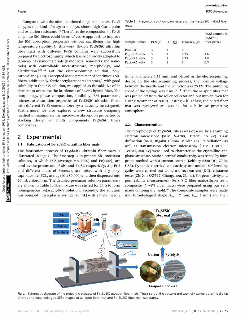
Table 1 Precursor solution parameters of the Fe3Si/SiC hybrid fibermats
Sample names PCS (g) PCL (g) Fe(acac)3 (g)
Fe3Si content inFe3Si/SiCber (wt%)
Pure SiC 3 1 0 0Fe3Si-1.6 wt% 3 1 0.25 1.6Fe3Si-3.8 wt% 3 1 0.75 3.8Fe3Si-6.5 wt% 3 1 1 6.5
Paper RSC Advances
Ope
n A
cces
s A
rtic
le. P
ublis
hed
on 2
8 Se
ptem
ber
2018
. Dow
nloa
ded
on 1
/16/
2022
6:1
6:14
AM
. T
his
artic
le is
lice
nsed
und
er a
Cre
ativ
e C
omm
ons
Attr
ibut
ion-
Non
Com
mer
cial
3.0
Unp
orte
d L
icen
ce.
View Article Online
Compared with the aforementioned magnetic phases, Fe–Sialloy, as one kind of magnetic alloys, shows high Curie pointand oxidation resistance.31 Therefore, the composition of Fe–Sialloy into SiC bers could be an effective approach to improvethe EM absorption properties without sacricing the hightemperature stability. In this work, exible Fe3Si/SiC ultrathinber mats with different Fe3Si contents were successfullyprepared by electrospinning, which has been widely adopted tofabricate 1D nano-materials (nanobers, nano-nets and nano-rods) with controllable microstructure, morphology, anddistribution.2,32–34 For the electrospinning solution, poly-carbosilane (PCS) is accepted as the precursor of continuous SiCbers. Additionally, ferric acetylacetonate (Fe(acac)3), with goodsolubility in the PCS solution, was applied as the additive of Feelement to overcome the brittleness of Fe/SiC hybrid ber. Themorphology, phase composition, exibility, EM parameters,microwave absorption properties of Fe3Si/SiC ultrathin berswith different Fe3Si contents were systematically investigated.Furthermore, we also explored a new structure designingmethod to manipulate the microwave absorption properties bystacking design of multi components Fe3Si/SiC berscomposites.
2 Experimental2.1. Fabrication of Fe3Si/SiC ultrathin ber mats
The fabrication process of Fe3Si/SiC ultrathin ber mats isillustrated in Fig. 1. The rst step is to prepare SiC precursorsolution, in which PCS (average Mn 2000) and Fe(acac)3 areused as the precursors of SiC and Fe3Si, respectively. 3 g PCSand different mass of Fe(acac)3 are mixed with 1 g poly-caprolactone (PCL, average Mn 80 000) and then dispersed into20 mL chloroform. The detailed precursor solution parametersare shown in Table 1. The mixture was stirred for 24 h to formhomogeneous Fe(acac)3/PCS solution. Secondly, the solutionwas pumped into a plastic syringe (20 mL) with a metal needle
Fig. 1 Schematic diagram of the preparing process of Fe3Si/SiC ultrathinphotos and local enlarged SEM images of as-spun fiber mat and Fe3Si/S
This journal is © The Royal Society of Chemistry 2018
(inner diameter: 0.51 mm) and placed in the electrospinningdevice. In the electrospinning process, the positive voltagebetween the needle and the collector was 25 kV. The pumpingspeed of the syringe was 2 mL h�1. Then the as-spun ber matwas peeled off from the roller collector and put into an oven forcuring treatment at 200 �C lasting 2 h. At last, the cured bermat was pyrolyzed at 1400 �C for 2 h in Ar protectingatmosphere.
2.2. Characterization
The morphology of Fe3Si/SiC bers was observe by a scanningelectron microscope (SEM, S-4700, Hitachi, 15 kV). X-raydiffraction (XRD, Rigaku Ultima IV with Cu Ka radiation) aswell as transmission electron microscopy (TEM, F-30 FEI-Tecnai, 300 kV) were used to characterize the crystalline andphase structure. Static electrical conductivity was tested by four-probe method with a current source (Keithley 6220 DC; Ohio,USA). Dynamic electrical conductivity test under 180�-bendingcycles were carried out using a direct current (DC) resistancetester (Zhi Xin ZX5512, Changzhou, China). For permittivity andpermeability measurement, Fe3Si/SiC ber mats/silicon resincomposite (5 wt% ber mats) were prepared using our self-made tamping die mold.30 The composite samples were madeinto toroid-shaped shape (Dout: 7 mm, Din: 3 mm) and then
fiber mats. The insets at the bottom and top right corners are the digitaliC fiber mat, separately.
RSC Adv., 2018, 8, 33574–33582 | 33575

RSC Advances Paper
Ope
n A
cces
s A
rtic
le. P
ublis
hed
on 2
8 Se
ptem
ber
2018
. Dow
nloa
ded
on 1
/16/
2022
6:1
6:14
AM
. T
his
artic
le is
lice
nsed
und
er a
Cre
ativ
e C
omm
ons
Attr
ibut
ion-
Non
Com
mer
cial
3.0
Unp
orte
d L
icen
ce.
View Article Online
placed in the coaxial line mode of Agilent vector network ana-lyser HP8722D to measure and calculate complex permittivity(3r ¼ 30 � j300) and permeability (mr ¼ m0 � jm00).
Based on transmission-line theory and metal back-panelmodel,35–37 the reection loss (RL) values were calculated by 3r
and mr to evaluate the microwave absorption properties.
RL ¼ 20 log10|(Zin � Z0)/(Zin + Z0)| (1)
Z0 ¼ (m0/30)1/2 (2)
Zin ¼ Z0 (mr/3r)1/2 tanh[j(2pfd/c)(mr3r)
1/2] (3)
where Zin means the impedance of the composite backed by theground plane, Z0 is the intrinsic impedance of free space, f is thefrequency of incident EMwaves, d is the thickness of absorber, cis the speed of light.
Fig. 2 (a)–(f) SEM images of Fe3Si/SiC hybrid fibers with different Fe3Sicontents: (a and b) Fe3Si-1.6 wt%; (c and d) Fe3Si-3.8 wt%; (e and f)Fe3Si-6.5 wt%. (g and h) EDS mapping images (Fe and Si) of Fe3Si-3.8 wt% sample.
3 Results and discussion3.1. Microstructure and chemical composition
The diameter of pure SiC bers is around 5 mm (as shown inFig. S1†). As the introducing of Fe3Si phase, the diameter ofFe3Si/SiC hybrid bers (Fig. 2(a)–(f)) greatly drops to 1–2 mm.The reduction of ber size is mainly contributed from theadding of Fe(acac)3 in the PCS solution, which enhances theelectrical conductivity and spinnability of the precursor solu-tion. In the process of electrospinning, a jet of the pendantdroplet at the tip of needle becomes highly electried when thehigh voltage is applied. And the droplet will form into a conicalshape called Taylor cone, from which a liquid jet will be ejectedout once the electric energy surpasses the surface free energy ofthe electrospun solution. With the introduction of Fe(acac)3,there would be a larger charge density on the surface of Taylorcone, so more electric charges could be loaded by the solutionjet.34,38 Such effect was also observed and reported in the elec-trospun polymer nanobers with salts additive.39,40 And thecrystallization degree, exibility and EM properties of Fe3Si/SiCbers will also be further inuenced by the adding of Fe(acac)3and the reduction of bers diameter, which would be discussedlater. As the Fe3Si content increased from 1.6 to 3.8 wt%,nanoparticles with the average size of 500 nm appear on thesurface of Fe3Si/SiC bers (Fig. 2(c) and (d)). And the nano-particles' number further rises when the Fe3Si content increasesto 6.5 wt% (Fig. 2(e) and (f)). According to the EDS elementmapping images of an individual Fe3Si-3.8 wt% ber in Fig. 2(g)and (h), Si is uniformly distributed in the whole ber while Fe ismainly concentrated in the nanoparticles, implying that thenanoparticles might be made of Fe3Si phase, which will beelaborated in the following parts.
To further verify the crystal structure and phase distributionof Fe3Si/SiC hybrid bers, the transmission electron microscopy(TEM) images and selected area electron diffraction (SAED)patterns detected form different parts (A and B in Fig. 3(a)) wereacquired and presented in Fig. 3(a)–(e). The high-resolutionTEM (HRTEM) image of area A (Fig. 3(b)) reveals a distinguish-able lattice spacing of 0.25 nm, matching the spacing of the
33576 | RSC Adv., 2018, 8, 33574–33582
(111) plane of b-SiC.15,41 Meanwhile, Fe3Si phase, together withSiC phase was also detected in the SAED patterns of area A(Fig. 3(c)), which is formed from the adding of Fe(acac)3 in theprecursor during the pyrolysis process.
In the nanoparticle part, the lattice spacing of 0.20 nm inarea B (Fig. 3(d)) agrees well with the (220) plane of Fe3Siphase.42,43 Carbon phase is usually existed in SiC ceramicfabricated by polymer-derived ceramic (PDC) and originatedfrom the pyrolysis PCS precursor.29 From Fig. 3(d) it is alsofound that a thin graphite layer with the thickness of 5–10 nmwas coated on the surface of nanoparticles.22 Moreover, SAEDpatterns in Fig. 3(e) further conrm the existence of Fe3Siphase44 and graphite.45 However, SiC phase is not observed inarea B from the results in Fig. 3(d) and (e). Therefore, it can beveried that Fe3Si phase is mainly concentrated in the nano-particles (area B). While in the ber part (area A), SiC and Fe3Siphase are coexisted.
The X-ray diffraction (XRD) patterns of pure SiC bers andFe3Si/SiC hybrid bers were compared and exhibited inFig. 4(a). The diffraction peaks of b-SiC (JCPDS#74-2307; 35.6�,60.0� and 71.8�)21 are observed in all the patterns, whichbecome much sharper as the Fe3Si content increased from 0 to6.5 wt%, implying that the crystalline size are getting larger.
This journal is © The Royal Society of Chemistry 2018

Fig. 3 (a) TEM image of a single Fe3Si/SiC (Fe3Si-3.8 wt%) fiber; HRTEM and SAED images of the (b and c) fiber part (area A) and (d and e)nanoparticle part (area B) of the hybrid fiber.
Paper RSC Advances
Ope
n A
cces
s A
rtic
le. P
ublis
hed
on 2
8 Se
ptem
ber
2018
. Dow
nloa
ded
on 1
/16/
2022
6:1
6:14
AM
. T
his
artic
le is
lice
nsed
und
er a
Cre
ativ
e C
omm
ons
Attr
ibut
ion-
Non
Com
mer
cial
3.0
Unp
orte
d L
icen
ce.
View Article Online
Actually, the adding of Fe(acac)3 in the PCS solution canpromote the formation of SiC phase, which is attributed to theFe element acting as the catalyst when SiC crystal was formedfrom PCS precursor.30,46 In addition, Fe3Si phase is also detectedwith the peaks at 45.3�, 66.1� and 83.7� (JCPDS#45-1207)47 forFe3Si/SiC hybrid bers, corresponding to the HRTEM and SAEDresults in Fig. 3(c)–(e). The Fe3Si phase was formed fromFe(acac)3 in the heat treatment process. Fe(acac)3 was convertedto Fe3O4 at relatively low pyrolysis temperature (<800 �C) andreduced into Fe3Si in Si-rich environment at high temperature(>800 �C). The conversion process was described in detail in ourlast article.30 Fig. 4(b) shows the hysteresis loops of Fe3Si/SiChybrid bers with different Fe3Si contents, it can be seen thatthe hybrid bers demonstrate ferromagnetic behaviour,resulting from the Fe3Si phase with a half-metallic property.42,48
For the sample of Fe3Si-1.6/3.8/6.5 wt%, the related saturation
Fig. 4 (a) XRD patterns of pure SiC fibers and Fe3Si/SiC hybrid fibers whybrid fibers with different Fe3Si contents.
This journal is © The Royal Society of Chemistry 2018
magnetization (Ms) values are 2.5/5.0/8.4 emu g�1, separately.Meanwhile, the coercivity (Hc) of Fe3Si-1.6 wt% and 6.5 wt% areabout 50 Oe, while the Hc of Fe3Si-3.8 wt% slightly grows to 90Oe.
180� bending test was performed to evaluate the exibility ofFe3Si/SiC hybrid ber mats. The testing sample of pure SiC bermat was broken in two pieces even at the rst bending cycle (asshown in Fig. S2†), implying a very brittle feature. By compar-ison, the exibility is drastically improved for Fe3Si/SiC hybridber mats. In the process of 500 times bending test, as shown inFig. 5, the electric resistance changing ratio (DR/R0) of Fe3Si-1.6 wt% and Fe3Si-3.8 wt% remained below 1%, meaning thebers kept intact in the whole testing process. Such enhancedexibility is owing to the smaller ber diameter and highercrystallization degree than pure SiC bers.31,49 However, as theFe3Si content further increased to 6.3 wt%, the DR/R0 value
ith different Fe3Si; (b) room-temperature hysteresis loops of Fe3Si/SiC
RSC Adv., 2018, 8, 33574–33582 | 33577
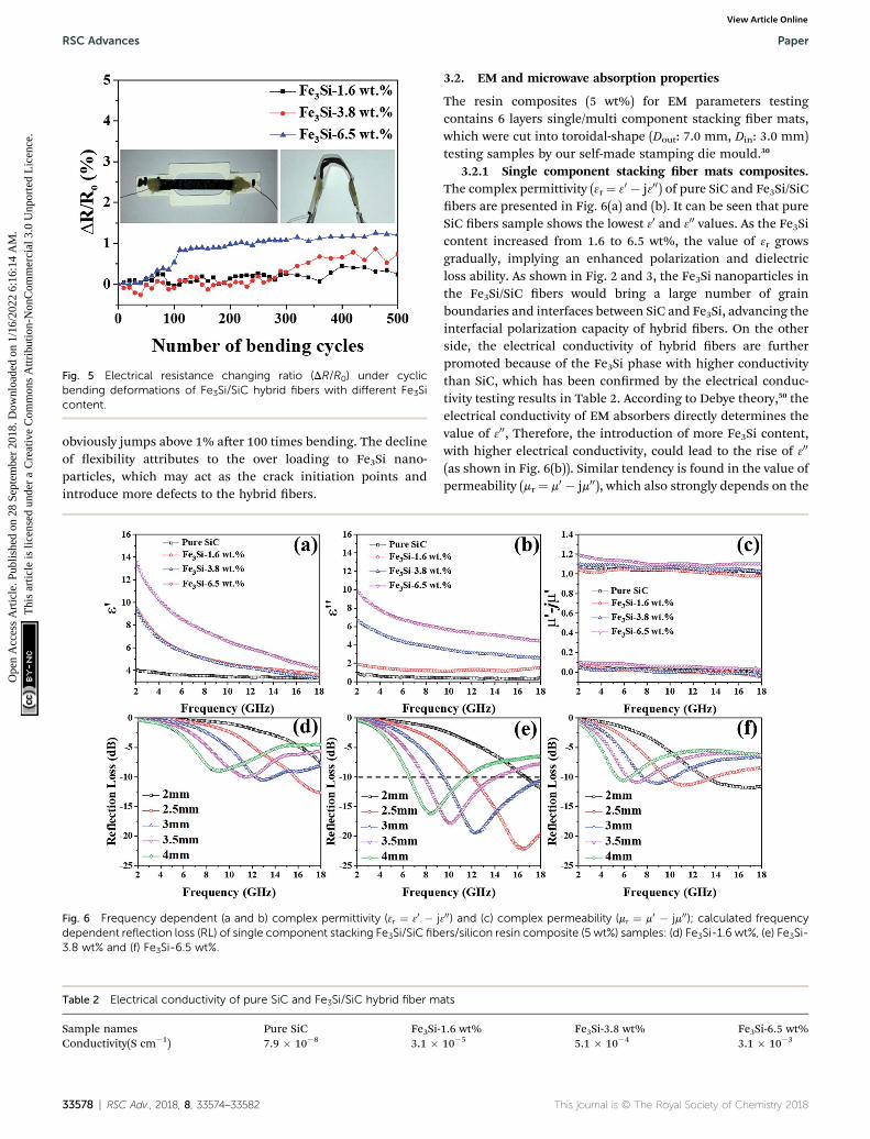
Fig. 5 Electrical resistance changing ratio (DR/R0) under cyclicbending deformations of Fe3Si/SiC hybrid fibers with different Fe3Sicontent.
RSC Advances Paper
Ope
n A
cces
s A
rtic
le. P
ublis
hed
on 2
8 Se
ptem
ber
2018
. Dow
nloa
ded
on 1
/16/
2022
6:1
6:14
AM
. T
his
artic
le is
lice
nsed
und
er a
Cre
ativ
e C
omm
ons
Attr
ibut
ion-
Non
Com
mer
cial
3.0
Unp
orte
d L
icen
ce.
View Article Online
obviously jumps above 1% aer 100 times bending. The declineof exibility attributes to the over loading to Fe3Si nano-particles, which may act as the crack initiation points andintroduce more defects to the hybrid bers.
Fig. 6 Frequency dependent (a and b) complex permittivity (3r ¼ 30 � jdependent reflection loss (RL) of single component stacking Fe3Si/SiC fib3.8 wt% and (f) Fe3Si-6.5 wt%.
Table 2 Electrical conductivity of pure SiC and Fe3Si/SiC hybrid fiber m
Sample names Pure SiC Fe3Si-Conductivity(S cm�1) 7.9 � 10�8 3.1 �
33578 | RSC Adv., 2018, 8, 33574–33582
3.2. EM and microwave absorption properties
The resin composites (5 wt%) for EM parameters testingcontains 6 layers single/multi component stacking ber mats,which were cut into toroidal-shape (Dout: 7.0 mm, Din: 3.0 mm)testing samples by our self-made stamping die mould.30
3.2.1 Single component stacking ber mats composites.The complex permittivity (3r ¼ 30 � j300) of pure SiC and Fe3Si/SiCbers are presented in Fig. 6(a) and (b). It can be seen that pureSiC bers sample shows the lowest 30 and 300 values. As the Fe3Sicontent increased from 1.6 to 6.5 wt%, the value of 3r growsgradually, implying an enhanced polarization and dielectricloss ability. As shown in Fig. 2 and 3, the Fe3Si nanoparticles inthe Fe3Si/SiC bers would bring a large number of grainboundaries and interfaces between SiC and Fe3Si, advancing theinterfacial polarization capacity of hybrid bers. On the otherside, the electrical conductivity of hybrid bers are furtherpromoted because of the Fe3Si phase with higher conductivitythan SiC, which has been conrmed by the electrical conduc-tivity testing results in Table 2. According to Debye theory,50 theelectrical conductivity of EM absorbers directly determines thevalue of 300, Therefore, the introduction of more Fe3Si content,with higher electrical conductivity, could lead to the rise of 300
(as shown in Fig. 6(b)). Similar tendency is found in the value ofpermeability (mr ¼ m0 � jm00), which also strongly depends on the
300) and (c) complex permeability (mr ¼ m0 � jm00); calculated frequencyers/silicon resin composite (5 wt%) samples: (d) Fe3Si-1.6 wt%, (e) Fe3Si-
ats
1.6 wt% Fe3Si-3.8 wt% Fe3Si-6.5 wt%10�5 5.1 � 10�4 3.1 � 10�3
This journal is © The Royal Society of Chemistry 2018

Fig. 7 Stacking design of multi components stacking fiber matscomposites.
Paper RSC Advances
Ope
n A
cces
s A
rtic
le. P
ublis
hed
on 2
8 Se
ptem
ber
2018
. Dow
nloa
ded
on 1
/16/
2022
6:1
6:14
AM
. T
his
artic
le is
lice
nsed
und
er a
Cre
ativ
e C
omm
ons
Attr
ibut
ion-
Non
Com
mer
cial
3.0
Unp
orte
d L
icen
ce.
View Article Online
Fe3Si content (Fig. 6(c)). Since SiC is a dielectric ceramicmaterial, the magnetic resonance in mr is contributed by Fe3Siphase.
The reection loss (RL) of pure SiC and Fe3Si/SiC bers(depicted in Fig. S3† and 6(d)–(f)) are calculated to evaluate themicrowave absorption capacity by using eqn (1)–(3). Pure SiCbers sample (Fig. S3†) still shows the worst microwaveabsorption property and the RL values are above�5 dB with thesample thickness from 2–4 mm. For the sample of Fe3Si-1.6 wt%, the situation is slightly modied as shown in Fig. 6(d),where the minimal RL value decreases to �12.8 dB at 18 GHz at2.5 mm. As the Fe3Si content is further increased to 3.8 wt%,a remarkable improvement of the RL values is shown up(Fig. 6(e)). At 16.5 GHz and 2.5 mm thickness, the RL valuereaches�22.5 dB, associated with the effective absorption areas(EAB, RL <�10 dB, 90% absorption) as broad as 8.5 GHz (9.5–18GHz at 3 mm thickness). However, over loading of Fe3Si wouldlead to the decay of microwave absorption property. As illus-trated in Fig. 6(f), the minimal RL value of Fe3Si-6.3 wt% is only�11.9 dB at 17.0 GHz with the sample thickness of 2 mm. Thedrop of RL values should be blamed on the improper matchedcharacteristic impedance. Based on the back-panel model andl/4 cancellation theory, the maximum RL values would berealized when the phase difference between incident and re-ected wave at the air-absorber (AA) interface is 180�.51–53
Besides, the amplitudes of the two waves that related to 3r and mr
Fig. 8 Frequency dependent (a and b) complex permittivity (3r ¼ 30 � jstacking Fe3Si/SiC fibers/silicon resin composite (5 wt%) samples.
This journal is © The Royal Society of Chemistry 2018
have to be equal in order to achieve the optimal cancellationscenario. If the characteristic impedance matches well, moremicrowave would enter the absorbers and be dissipated.Otherwise the microwave would mostly be reected in thesurface of absorbers. The modulus of Zin � 1 (|Zin � 1|) thatcalculated by eqn (2) and (3) is used to evaluate the character-istic impedance matching degree. As shown in Fig. S4†, the |Zin� 1| value of pure SiC bers is far away from 0 in the wholefrequency range, meaning that the characteristic impedance ismismatched. As for the Fe3Si/SiC hybrid bers, the |Zin � 1|value of Fe3Si-3.8 wt% sample gets closest to zero, then followedby Fe3Si-6.5 wt% and Fe3Si-1.6 wt% separately. As a result, Fe3Si-3.8 wt% sample exhibits the best characteristic impedancematching degree and consequently has the lowest RL values.Moreover, it is worth noticing that introducing Fe3Si phase intoSiC bers could apparently shi the RL peaks to lowerfrequency range, and the shiing degree is enhanced with theincreasing content of Fe3Si. Such effect should be ascribed tothe magnetic loss that introduced by Fe3Si phase, which hasbeen conrmed and discussed in our last report.29
3.2.2 Multi components stacking ber mats composites.The Fe3Si/SiC hybrid ber mats composites stacked by multicomponents ber layers were also prepared to further enhancethe RL values and then manipulate the microwave absorptionparameters. As shown in Fig. 7, different numbers of low Fe3Sicontent layers (Fe3Si-1.6 wt%) and high Fe3Si content layers(Fe3Si-6.5 wt%) were stacked to form 6 layers' Fe3Si/SiC bers/silicon resin composite (5 wt%) samples.
The EM parameters of multi components stacking ber matscomposites were measured and presented in Fig. 8. With thenumber of high Fe3Si content layer increased from 1–5, thepolarization and dielectric loss ability of the stacking ber matscomposite would be gradually advanced, hence, both 30 and 300
are slightly promoted in most frequency range (shown inFig. 8(a) and (b)). It means that the permittivity of Fe3Si/SiCbers/silicon resin composites can be easily tuned by thestacking component designing. In addition, since the Fe3Sicontent in our prepared Fe3Si/SiC hybrid bers is less than 7%,the magnetic loss would not play a dominated role in the EMproperties of multi components stacking bermats composites,corresponding with the results in Fig. 8(c) that no obviousdifference is found in the permeability (mr ¼ m0 � jm00) curves.
300) and (c) complex permeability (mr ¼ mʹ � jm00) of multi components
RSC Adv., 2018, 8, 33574–33582 | 33579
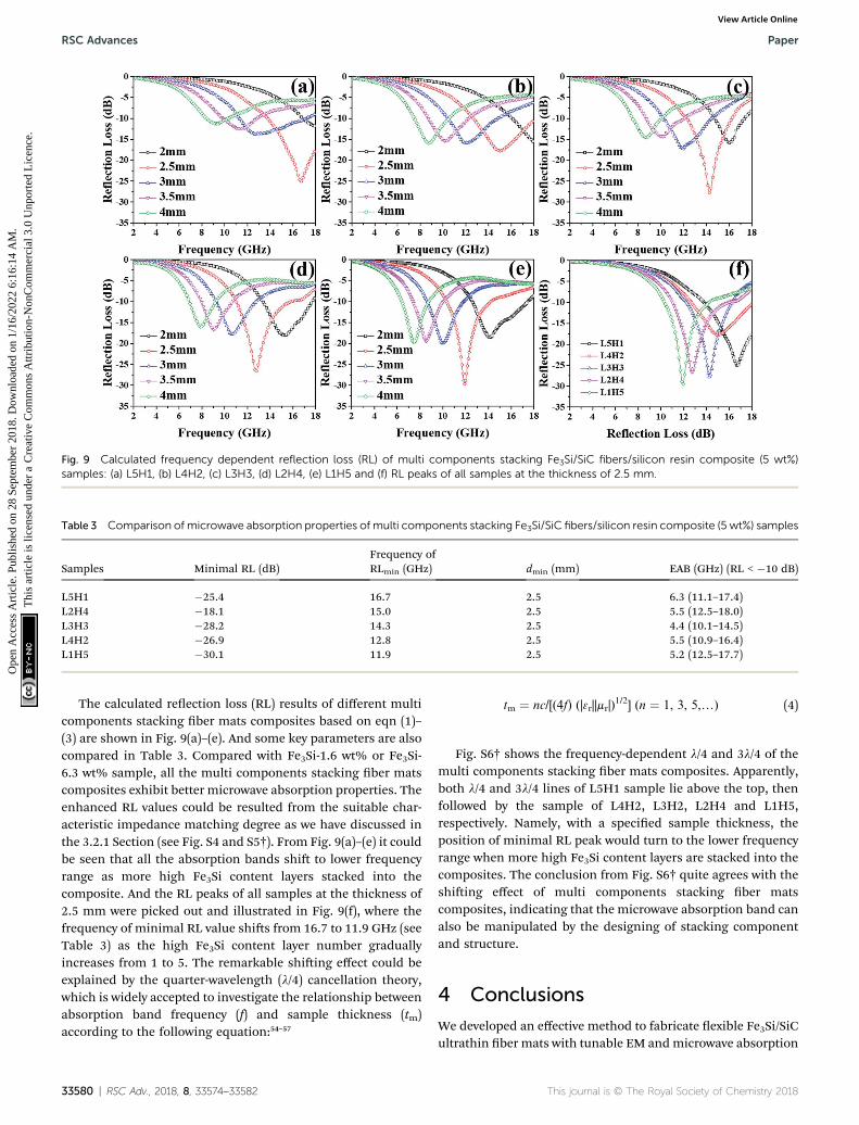
Fig. 9 Calculated frequency dependent reflection loss (RL) of multi components stacking Fe3Si/SiC fibers/silicon resin composite (5 wt%)samples: (a) L5H1, (b) L4H2, (c) L3H3, (d) L2H4, (e) L1H5 and (f) RL peaks of all samples at the thickness of 2.5 mm.
Table 3 Comparison of microwave absorption properties of multi components stacking Fe3Si/SiC fibers/silicon resin composite (5 wt%) samples
Samples Minimal RL (dB)Frequency ofRLmin (GHz) dmin (mm) EAB (GHz) (RL < �10 dB)
L5H1 �25.4 16.7 2.5 6.3 (11.1–17.4)L2H4 �18.1 15.0 2.5 5.5 (12.5–18.0)L3H3 �28.2 14.3 2.5 4.4 (10.1–14.5)L4H2 �26.9 12.8 2.5 5.5 (10.9–16.4)L1H5 �30.1 11.9 2.5 5.2 (12.5–17.7)
RSC Advances Paper
Ope
n A
cces
s A
rtic
le. P
ublis
hed
on 2
8 Se
ptem
ber
2018
. Dow
nloa
ded
on 1
/16/
2022
6:1
6:14
AM
. T
his
artic
le is
lice
nsed
und
er a
Cre
ativ
e C
omm
ons
Attr
ibut
ion-
Non
Com
mer
cial
3.0
Unp
orte
d L
icen
ce.
View Article Online
The calculated reection loss (RL) results of different multicomponents stacking ber mats composites based on eqn (1)–(3) are shown in Fig. 9(a)–(e). And some key parameters are alsocompared in Table 3. Compared with Fe3Si-1.6 wt% or Fe3Si-6.3 wt% sample, all the multi components stacking ber matscomposites exhibit better microwave absorption properties. Theenhanced RL values could be resulted from the suitable char-acteristic impedance matching degree as we have discussed inthe 3.2.1 Section (see Fig. S4 and S5†). From Fig. 9(a)–(e) it couldbe seen that all the absorption bands shi to lower frequencyrange as more high Fe3Si content layers stacked into thecomposite. And the RL peaks of all samples at the thickness of2.5 mm were picked out and illustrated in Fig. 9(f), where thefrequency of minimal RL value shis from 16.7 to 11.9 GHz (seeTable 3) as the high Fe3Si content layer number graduallyincreases from 1 to 5. The remarkable shiing effect could beexplained by the quarter-wavelength (l/4) cancellation theory,which is widely accepted to investigate the relationship betweenabsorption band frequency (f) and sample thickness (tm)according to the following equation:54–57
33580 | RSC Adv., 2018, 8, 33574–33582
tm ¼ nc/[(4f) (|3r||mr|)1/2] (n ¼ 1, 3, 5,.) (4)
Fig. S6† shows the frequency-dependent l/4 and 3l/4 of themulti components stacking ber mats composites. Apparently,both l/4 and 3l/4 lines of L5H1 sample lie above the top, thenfollowed by the sample of L4H2, L3H2, L2H4 and L1H5,respectively. Namely, with a specied sample thickness, theposition of minimal RL peak would turn to the lower frequencyrange when more high Fe3Si content layers are stacked into thecomposites. The conclusion from Fig. S6† quite agrees with theshiing effect of multi components stacking ber matscomposites, indicating that the microwave absorption band canalso be manipulated by the designing of stacking componentand structure.
4 Conclusions
We developed an effective method to fabricate exible Fe3Si/SiCultrathin ber mats with tunable EM andmicrowave absorption
This journal is © The Royal Society of Chemistry 2018

Paper RSC Advances
Ope
n A
cces
s A
rtic
le. P
ublis
hed
on 2
8 Se
ptem
ber
2018
. Dow
nloa
ded
on 1
/16/
2022
6:1
6:14
AM
. T
his
artic
le is
lice
nsed
und
er a
Cre
ativ
e C
omm
ons
Attr
ibut
ion-
Non
Com
mer
cial
3.0
Unp
orte
d L
icen
ce.
View Article Online
properties by component and structure design. Fe(acac)3 wasselected as the Fe source in the PCS solution, which trans-formed into Fe3Si phase in the Fe3Si/SiC hybrid bers.Compared with pure SiC bers, the Fe3Si/SiC hybrid bers showsmaller diameter of 1–2 mm. The exibility of Fe3Si/SiC hybridber mats (Fe3Si-1.6 and 3.8 wt%) are also greatly enhanced andremained undamaged aer 500 times' 180� bending testing.Furthermore, the composition of Fe3Si phase could bringimprovement to the electrical conductivity and EM attenuationability, associated with higher dielectric and magnetic loss. Atthe optimal Fe3Si content of 3.8 wt%, the Fe3Si/SiC bers/siliconresin composite (5 wt%) could reach a minimal RL value of�22.5 dB at 16.5 GHz and 2.5 mm thickness with the EAB valueas broad as 8.5 GHz. By varying the stacking structure of multicomponents stacking ber mats composites, the microwaveabsorption performance can be further promoted andmanipulated.
Conflicts of interest
There are no conicts to declare.
Acknowledgements
This work was supported by the National Key R&D Program ofChina (No. 2017YFB1103500). And we would like to thank theAnalytical & Testing Center of Northwestern PolytechnicalUniversity for the supporting of TEM testing.
Notes and references
1 X. Jin, X. Fan, C. Lu and T. Wang, J. Eur. Ceram. Soc., 2018,38, 1–28.
2 R. Wu, K. Zhou, C. Y. Yue, J. Wei and Y. Pan, Prog. Mater. Sci.,2015, 72, 1–60.
3 M. Belmonte, Adv. Eng. Mater., 2006, 8, 693–703.4 L. Su, H. Wang, M. Niu, X. Fan, M. Ma, Z. Shi and S.-W. Guo,ACS Nano, 2018, 12, 3103–3111.
5 B. Sun, Y. Sun and C. Wang, Small, 2018, 14, 1703391.6 L. Cheng, Y. Xu, L. Zhang and X. Yin, Composites, Part A,2000, 31, 1015–1020.
7 X. Ma, X. Yin, X. Fan, X. Sun, L. Yang, F. Ye and L. Cheng, J.Eur. Ceram. Soc., 2018, 38, 1069–1078.
8 I. Spitsberg and J. Steibel, Int. J. Appl. Ceram. Technol., 2004,1, 291–301.
9 R. Naslain, Compos. Sci. Technol., 2004, 64, 155–170.10 Y. Katoh, K. Ozawa, C. Shih, T. Nozawa, R. J. Shinavski,
A. Hasegawa and L. L. Snead, J. Nucl. Mater., 2014, 448,448–476.
11 Y. Katoh, L. L. Snead, C. H. Henager, T. Nozawa, T. Hinoki,A. Ivekovic, S. Novak and S. G. De Vicente, J. Nucl. Mater.,2014, 455, 387–397.
12 M. Han, X. Yin, Z. Hou, C. Song, X. Li, L. Zhang andL. Cheng, ACS Appl. Mater. Interfaces, 2017, 9, 11803–11810.
13 X. Yin, L. Kong, L. Zhang, L. Cheng, N. Travitzky and P. Greil,Int. Mater. Rev., 2014, 59, 326–355.
This journal is © The Royal Society of Chemistry 2018
14 A. Mathur, S. B. Dutta, D. Pal, J. Singhal, A. Singh andS. Chattopadhyay, Adv. Mater. Interfaces, 2016, 3, 1600413.
15 B. Wang, Y. Wang, Y. Lei, N. Wu, Y. Gou, C. Han, S. Xie andD. Fang, Nano Res., 2016, 9, 886–898.
16 A. Oliveros, A. Guiseppi-Elie and S. E. Saddow, Biomed.Microdevices, 2013, 15, 353–368.
17 S. C. Chiu, H. C. Yu and Y. Y. Li, J. Phys. Chem. C, 2010, 114,1947–1952.
18 J. Kuang and W. Cao, Appl. Phys. Lett., 2013, 103, 112906.19 J. Kuang, P. Jiang, W. Liu and W. Cao, Appl. Phys. Lett., 2015,
106, 212903.20 S. Sarkar, J. Zou, J. Liu, C. Xu, L. An and L. Zhai, ACS Appl.
Mater. Interfaces, 2010, 2, 1150–1156.21 L. P. Rajukumar, M. Belmonte, J. E. Slimak, A. L. Elıas,
E. Cruz-Silva, N. Perea-Lopez, A. Morelos-Gomez,H. Terrones, M. Endo and P. Miranzo, Adv. Funct. Mater.,2015, 25, 4985–4993.
22 P. Wang, L. Cheng, Y. Zhang, H. Wu, Y. Hou, W. Yuan andL. Zheng, Ceram. Int., 2017, 43, 7424–7435.
23 Y. Cheng, M. Tan, P. Hu, X. Zhang, B. Sun, L. Yan, S. Zhouand W. Han, Appl. Surf. Sci., 2018, 448, 138–144.
24 X. Huang, X. Yan, L. Xia, P. Wang, Q. Wang, X. Zhang,B. Zhong, H. Zhao and G. Wen, Scr. Mater., 2016, 120, 107–111.
25 M. Sun, X. Lv, A. Xie, W. Jiang and F. Wu, J. Mater. Chem. C,2016, 4, 8897–8902.
26 J. Kuang, P. Jiang, F. Ran and W. Cao, J. Alloys Compd., 2016,687, 227–231.
27 C. Liang, C. Liu, H. Wang, L. Wu, Z. Jiang, Y. Xu, B. Shen andZ. Wang, J. Mater. Chem. A, 2014, 2, 16397–16402.
28 H. Wang, L. Wu, J. Jiao, J. Zhou, Y. Xu, H. Zhang, Z. Jiang,B. Shen and Z. Wang, J. Mater. Chem. A, 2015, 3, 6517–6525.
29 Y. Hou, L. Cheng, Y. Zhang, Y. Yang, C. Deng, Z. Yang,Q. Chen, P. Wang and L. Zheng, ACS Appl. Mater.Interfaces, 2017, 9, 7265–7271.
30 Y. Hou, L. Cheng, Y. Zhang, Y. Yang, C. Deng, Z. Yang,Q. Chen, X. Du and L. Zheng, ACS Appl. Mater. Interfaces,2017, 9, 43072–43080.
31 Y. Hou, B. Xiao, G. Yang, Z. Sun, W. Yang, S. Wu, X. Huangand G. Wen, J. Mater. Chem. C, 2018, 6, 7661–7670.
32 X. Wang, B. Ding, G. Sun, M. Wang and J. Yu, Prog. Mater.Sci., 2013, 58, 1173–1243.
33 D. Li and Y. Xia, Adv. Mater., 2004, 16, 1151–1170.34 D. Li, J. T. McCann, Y. Xia and M. Marquez, J. Am. Ceram.
Soc., 2006, 89, 1861–1869.35 P. Miles, W. Westphal and A. Von Hippel, Rev. Mod. Phys.,
1957, 29, 279.36 F. Ye, Q. Song, Z. Zhang, W. Li, S. Zhang, X. Yin, Y. Zhou,
H. Tao, Y. Liu and L. Cheng, Adv. Funct. Mater., 2018,1707205.
37 L. Kong, C. Wang, X. Yin, X. Fan, W. Wang and J. Huang, J.Mater. Chem. C, 2017, 5, 7479–7488.
38 K.-H. Chang and H.-L. Lin, J. Polym. Res., 2009, 16, 611–622.39 N. A. M. Barakat, M. A. Kanjwal, F. A. Sheikh and H. Y. Kim,
Polymer, 2009, 50, 4389–4396.40 M. M. Demir, I. Yilgor, E. Yilgor and B. Erman, Polymer,
2002, 43, 3303–3309.
RSC Adv., 2018, 8, 33574–33582 | 33581

RSC Advances Paper
Ope
n A
cces
s A
rtic
le. P
ublis
hed
on 2
8 Se
ptem
ber
2018
. Dow
nloa
ded
on 1
/16/
2022
6:1
6:14
AM
. T
his
artic
le is
lice
nsed
und
er a
Cre
ativ
e C
omm
ons
Attr
ibut
ion-
Non
Com
mer
cial
3.0
Unp
orte
d L
icen
ce.
View Article Online
41 L. Wang, G. Wei, F. Gao, C. Li and W. Yang, Nanoscale, 2015,7, 7585–7592.
42 J. Thomas, J. Schumann, H. Vinzelberg, E. Arushanov,R. Engelhard, O. Schmidt and T. Gemming,Nanotechnology, 2009, 20, 235604.
43 C. Deneke, J. Schumann, R. Engelhard, J. Thomas, C. Muller,M. Khatri, A. Malachias, M. Weisser, T. Metzger andO. Schmidt, Nanotechnology, 2008, 20, 045703.
44 Y. Jing, S.-H. He and J.-P. Wang, J. Nanopart. Res., 2013, 15,1517.
45 X. Sun, K. Sun, C. Chen, H. Sun and B. Cui, Int. J. Mater.Chem., 2012, 2, 218–224.
46 Z. Yu, L. Yang, H. Min, P. Zhang, C. Zhou and R. Riedel, J.Mater. Chem. C, 2014, 2, 1057–1067.
47 C. Vakifahmetoglu, E. Pippel, J. Woltersdorf andP. Colombo, J. Am. Ceram. Soc., 2010, 93, 959–968.
48 Y. Kobayashi, T. Kaneko, M. Kamogawa, K. Asai, K. Akiyamaand H. Funakubo, J. Phys. D: Appl. Phys., 2007, 40, 6873.
33582 | RSC Adv., 2018, 8, 33574–33582
49 S.-C. Wong, A. Baji and S. Leng, Polymer, 2008, 49, 4713–4722.
50 W. Duan, X. Yin, F. Ye, Q. Li, M. Han, X. Liu and Y. Cai, J.Mater. Chem. C, 2016, 4, 5962–5969.
51 T. Wang, R. Han, G. Tan, J. Wei, L. Qiao and F. Li, J. Appl.Phys., 2012, 112, 104903.
52 Z. Li, G. Lin and L. Kong, IEEE Trans. Magn., 2008, 44, 2255–2261.
53 T. Zhang, J. Zhang, G. Wen, B. Zhong, L. Xia, X. Huang,H. Zhao, H. Wang and L. Qin, Carbon, 2018, 136, 345–358.
54 B. Wang, J. Wei, Y. Yang, T. Wang and F. Li, J. Magn. Magn.Mater., 2011, 323, 1101–1103.
55 X. Li, H. Yi, J. Zhang, J. Feng, F. Li, D. Xue, H. Zhang, Y. Pengand N. J. Mellors, J. Nanopart. Res., 2013, 15, 1–11.
56 X. Li, J. Feng, Y. Du, J. Bai, H. Fan, H. Zhang, Y. Peng andF. Li, J. Mater. Chem. A, 2015, 3, 5535–5546.
57 X. Yuan, L. Cheng and L. Zhang, J. Alloys Compd., 2016, 680,604–611.
This journal is © The Royal Society of Chemistry 2018