Embed Size (px)
Citation preview

Flexible Clock Translator for GPON, Base Station, SONET/SDH, T1/E1, and Ethernet
AD9553
Rev. A Information furnished by Analog Devices is believed to be accurate and reliable. However, no responsibility is assumed by Analog Devices for its use, nor for any infringements of patents or other rights of third parties that may result from its use. Specifications subject to change without notice. No license is granted by implication or otherwise under any patent or patent rights of Analog Devices. Trademarks and registered trademarks are the property of their respective owners.
One Technology Way, P.O. Box 9106, Norwood, MA 02062-9106, U.S.A. Tel: 781.329.4700 www.analog.com Fax: 781.461.3113 ©2010 Analog Devices, Inc. All rights reserved.
FEATURES Input frequencies from 8 kHz to 710 MHz Output frequencies up to 810 MHz LVPECL and LVDS (up to
200 MHz for CMOS output) Preset pin-programmable frequency translation ratios cover
popular wireline and wireless frequency applications, including xDSL, T1/E1, BITS, SONET, and Ethernet
Arbitrary frequency translation ratios via SPI port On-chip VCO Accepts a crystal resonator for holdover applications Two single-ended (or one differential) reference input(s) Two output clocks (independently programmable as LVDS,
LVPECL, or CMOS) SPI-compatible, 3-wire programming interface Single supply (3.3 V) Very low power: <450 mW (under most conditions) Small package size (5 mm × 5 mm) Exceeds Telcordia GR-253-CORE jitter generation, transfer,
and tolerance specifications
APPLICATIONS Cost effective replacement of high frequency VCXO, OCXO,
and SAW resonators Extremely flexible frequency translation for SONET/SDH,
Ethernet, Fibre Channel, DRFI/DOCSIS, and PON/EPON/GPON
Wireless infrastructure Test and measurement (including handheld devices)
GENERAL DESCRIPTION The AD9553 is a phase-locked loop (PLL) based clock translator designed to address the needs of passive optical networks (PON) and base stations. The device employs an integer-N PLL to accommodate the applicable frequency translation requirements. The user supplies up to two single-ended input reference signals or one differential input reference signal via the REFA and REFB inputs. The device supports holdover applications by allowing the user to connect a 25 MHz crystal resonator to the XTAL input.
The AD9553 is pin programmable, providing a matrix of standard input/output frequency translations from a list of 15 possible input frequencies to a list of 52 possible output frequency pairs (OUT1 and OUT2). The device also has a 3-wire SPI interface, enabling the user to program custom input-to-output frequency translations.
The AD9553 output drivers are compatible with LVPECL, LVDS, or single-ended CMOS logic levels, although the AD9553 is implemented in a strictly CMOS process.
The AD9553 operates over the extended industrial temperature range of −40°C to +85°C.
BASIC BLOCK DIAGRAM
PLL OUTPUTCIRCUITRY
INPUTFREQUENCY
SOURCESELECTOR
REFA
REFB
XTAL
OUT2
OUT1
PIN-DEFINED AND SERIAL PROGRAMMING
AD9553
0856
5-00
1
Figure 1.

AD9553
Rev. A | Page 2 of 44
TABLE OF CONTENTS Features .............................................................................................. 1 Applications ....................................................................................... 1 General Description ......................................................................... 1 Basic Block Diagram ........................................................................ 1 Revision History ............................................................................... 2 Specifications ..................................................................................... 3
Power Consumption .................................................................... 3 Logic Input Pins ............................................................................ 3 Logic Output Pins ......................................................................... 3 RESET Pin ..................................................................................... 4 Reference Clock Input Characteristics ...................................... 4 VCO Characteristics .................................................................... 5 Crystal Input Characteristics ...................................................... 5 Output Characteristics ................................................................. 6 Jitter Characteristics ..................................................................... 7 Serial Control Port ....................................................................... 8 Serial Control Port Timing ......................................................... 8
Absolute Maximum Ratings ............................................................ 9 ESD Caution .................................................................................. 9
Pin Configuration and Function Descriptions ........................... 10 Typical Performance Characteristics ........................................... 11 Input/Output Termination Recommendations .......................... 15
Theory of Operation ...................................................................... 16 Overview ..................................................................................... 16 Preset Frequencies ...................................................................... 16 Device Control Modes ............................................................... 19 Description of Functional Blocks ............................................. 20 Jitter Tolerance ............................................................................ 26 Output/Input Frequency Relationship .................................... 26 Calculating Divider Values ....................................................... 27 Low Dropout (LDO) Regulators .............................................. 28 Automatic Power-On Reset ...................................................... 28
Applications Information .............................................................. 29 Thermal Performance ................................................................ 29
Serial Control Port ......................................................................... 30 Serial Control Port Pin Descriptions ....................................... 30 Operation of the Serial Control Port ....................................... 30 Instruction Word (16 Bits) ........................................................ 31 MSB/LSB First Transfers ........................................................... 31
Register Map ................................................................................... 33 Register Map Descriptions ........................................................ 35
Outline Dimensions ....................................................................... 42 Ordering Guide .......................................................................... 42
REVISION HISTORY 10/10—Rev. 0 to Rev. A Changes to Features Section, Applications Section, and General Description Section .......................................................................... 1 Added Table Summary to Specifications Section ......................... 3 Added Supply Voltage Parameter, Table 1 ..................................... 3 Changes to Table 5 ............................................................................ 4 Changes to Table 6 and Crystal Load Capacitance Parameter, Table 7 ................................................................................................ 5 Changes to Table 8 ............................................................................ 6 Changes to Table 9 ............................................................................ 7 Changes to Pin 1 and Pin 15, Table 13 ......................................... 10 Added Figure 4, Renumbered Sequentially ................................ 11 Added Figure 10, Figure 12, Figure 13, and Figure 14............... 12 Added Input/Output Termination Recommendations Section, Figure 25, Figure 26, and Figure 27 .............................................. 15 Moved Theory of Operation and Figure 28 ................................ 16 Changed General Description Section to Overview Section and Moved ............................................................................................... 16 Changes to Overview Section ....................................................... 16 Changes to Preset Frequencies Section and Table 14 ................ 17 Changes to Table 15 ........................................................................ 18
Changes to Table 16 ....................................................................... 19 Changes to PLL (PFD, Charge Pump, VCO, Feedback Divider Section .............................................................................................. 22 Changes to Loop Filter Section, Figure 31, Table 17, PLL Locked Indicator Section, and Output Dividers Section ........................ 23 Changes to Output Driver Mode Control Section ..................... 24 Changes to Output Driver Polarity (CMOS) Section ................ 25 Changes to Output/Input Frequency Relationship Section ...... 26 Changes to Calculating Divider Values Section ......................... 27 Changes to Automatic Power-On Reset Section ........................ 28 Changes to Thermal Performance Section ................................. 29 Changes to Address 0x18, Address 0x32, and Address 0x34, Table 27 ............................................................................................ 33 Changes to Address 0x18, Table 31 .............................................. 37 Change to Address 0x20, Table 34 ............................................... 38 Changes to Address 0x24, Table 35 and Address 0x28, Table 36 ... 39 Changes to Address 0x32, Table 37 .............................................. 40 Changes to Address 0x34, Table 39 .............................................. 41
4/10—Revision 0: Initial Version

AD9553
Rev. A | Page 3 of 44
SPECIFICATIONS Minimum (min) and maximum (max) values apply for the full range of supply voltage and operating temperature variations. Typical (typ) values apply for VDD = 3.3 V; TA = 25°C, unless otherwise noted.
POWER CONSUMPTION
Table 1. Parameter Min Typ Max Unit Test Conditions/Comments SUPPLY VOLTAGE 3.135 3.30 3.465 V Pin 18, Pin 21, and Pin 28 TOTAL CURRENT 162 185 mA Tested with both output channels active at
maximum output frequency; LVPECL and LVDS outputs use a 100 Ω termination between both pins of the output driver
VDD CURRENT BY PIN Tested with both output channels active at maximum output frequency; LVPECL and LVDS outputs use a 100 Ω termination between both pins of the output driver
Pin 18 93 106 mA Pin 21
LVDS Configured Output 35 41 mA LVPECL Configured Output 36 42 mA CMOS Configured Output 29 34 mA
Pin 28 LVDS Configured Output 35 41 mA LVPECL Configured Output 36 42 mA CMOS Configured Output 29 34 mA
LOGIC INPUT PINS Table 2. Parameter Min Typ Max Unit Test Conditions/Comments INPUT CHARACTERISTICS1
Logic 1 Voltage, VIH 1.02 V For the CMOS inputs, a static Logic 1 results from either a pull-up resistor or no connection
Logic 0 Voltage, VIL 0.64 V Logic 1 Current, IIH 3 µA Logic 0 Current, IIL 17 µA
1 The A3 to A0 and Y5 to Y0 pins have 100 kΩ internal pull-up resistors. The OM2 to OM0 pins have 40 kΩ pull-up resistors when the device is not in SPI mode.
LOGIC OUTPUT PINS Table 3. Parameter Min Typ Max Unit Test Conditions/Comments OUTPUT CHARACTERISTICS
Output Voltage High, VOH 2.7 V Tested at 1 mA load current Output Voltage Low, VOL 0.19 V Tested at 1 mA load current

AD9553
Rev. A | Page 4 of 44
RESET PIN
Table 4. Parameter Min Typ Max Unit Test Conditions/Comments INPUT CHARACTERISTICS1
Input Voltage High, VIH 1.96 V Input Voltage Low, VIL 0.85 V Input Current High, IINH 0.3 12.5 µA Input Current Low, IINL 31 43 µA
MINIMUM PULSE WIDTH LOW 150 µs Tested with an active source driving the RESET pin 1 The RESET pin has a 100 kΩ internal pull-up resistor.
REFERENCE CLOCK INPUT CHARACTERISTICS Table 5. Parameter Min Typ Max Unit Test Conditions/Comments DIFFERENTIAL INPUT
Input Frequency Range 0.008 250 MHz 710 MHz Assumes minimum LVDS input level and requires
bypassing of the divide-by-5 divider and ×2 multiplier Common-Mode Internally Generated
Input Voltage 613 692 769 mV Use ac coupling to preserve the internal dc bias of the
differential input Differential Input Voltage Sensitivity 250 mV p-p Requires ac coupling; can accommodate single-ended
input by ac grounding unused input; the instantaneous voltage on either pin must not exceed the 3.3 V dc supply rails
Differential Input Resistance 5 kΩ Differential Input Capacitance 3 pF Duty Cycle Pulse width high and pulse width low specifications
establish the bounds for duty cycle Pulse Width Low 1.6 ns Up to 250 MHz Pulse Width High 1.6 ns Up to 250 MHz Pulse Width Low 0.64 ns Beyond 250 MHz, up to 710 MHz Pulse Width High 0.64 ns Beyond 250 MHz, up to 710 MHz
CMOS SINGLE-ENDED INPUT Input Frequency Range 0.008 200 MHz Input High Voltage 1.62 V Input Low Voltage 0.52 V Input Threshold Voltage 1.0 V When ac coupling to the input receiver, the user must dc
bias the input to 1 V; the single-ended CMOS input is 3.3 V compatible
Input High Current 0.04 µA Input Low Current 0.03 µA Input Capacitance 3 pF Duty Cycle Pulse width high and pulse width low establish the
bounds for duty cycle Pulse Width Low 2 ns Pulse Width High 2 ns
×2 FREQUENCY MULTIPLIER 125 MHz To avoid excessive reference spurs, the ×2 multiplier requires 48% to 52% duty cycle; reference clock input frequencies greater than 125 MHz require the use of the divide-by-5 divider

AD9553
Rev. A | Page 5 of 44
VCO CHARACTERISTICS
Table 6. Parameter Min Typ Max Unit Test Conditions/Comments FREQUENCY RANGE 3350 4050 MHz VCO GAIN 45 MHz/V VCO TRACKING RANGE ±300 ppm VCO CALIBRATION TIME As measured from completion of the VCO calibration command
(the rising edge of CS (Pin 12)) until the rising edge of LOCKED (Pin 20)
Low Bandwidth Setting (170 Hz) Applies for Pin A3 to Pin A0 = 0001 to 1100, or for Pin A3 to Pin A0 = 1111
13.3 kHz PFD Frequency 214 ms 16 kHz PFD Frequency 176 ms
Medium Bandwidth Setting (20 kHz) Applies for Pin A3 to Pin A0 = 1110 and Pin Y5 to Pin Y0 = 111111 1.5625 MHz PFD Frequency 1.82 ms
High Bandwidth Setting (75 kHz) Applies for Pin A3 to Pin A0 = 1101 to 1110 2.64 MHz PFD Frequency 1.46 ms 4.86 MHz PFD Frequency 0.80 ms
PLL LOCK TIME Using the pin selected frequency settings; lock time is from the rising edge of the RESET pin to the rising edge of the LOCKED pin
Low Bandwidth Setting (170 Hz) Applies for Pin A3 to Pin A0 = 0001 to 1100 or for Pin A3 to Pin A0 = 1111
13.3 kHz PFD Frequency 214 ms 16 kHz PFD Frequency 176 ms
Medium Bandwidth Setting (20 kHz) Applies for Pin A3 to Pin A0 = 1110 and Pin Y5 to Pin Y0 = 111111 1.5625 MHz PFD Frequency 2 ms
High Bandwidth Setting (75 kHz) Applies for Pin A3 to Pin A0 = 1101 to 1110 2.64 MHz PFD Frequency 1.50 ms 4.86 MHz PFD Frequency 0.89 ms
CRYSTAL INPUT CHARACTERISTICS
Table 7. Parameter Min Typ Max Unit Test Conditions/Comments CRYSTAL FREQUENCY
Range 10 25 52 MHz When using the pin selected frequency settings, the device requires a 25 MHz crystal to support holdover functionality
Tolerance 20 ppm CRYSTAL MOTIONAL RESISTANCE 100 Ω CRYSTAL LOAD CAPACITANCE 10 pF Using a crystal with a specified load capacitance other than 10 pF
(8 pF to 24 pF) is possible, but necessitates using the SPI port to alter the default register values for load capacitance

AD9553
Rev. A | Page 6 of 44
OUTPUT CHARACTERISTICS
Table 8. Parameter Min Typ Max Unit Test Conditions/Comments LVPECL MODE
Differential Output Voltage Swing 690 800 890 mV Output driver static (for dynamic performance, see Figure 18)
Common-Mode Output Voltage VDD − 1.66 VDD − 1.34 VDD − 1.01 V Output driver static Frequency Range 0 810 MHz Duty Cycle 40 60 % Up to 805 MHz output frequency Rise/Fall Time1 (20% to 80%) 255 305 ps 100 Ω termination between both pins of the
output driver LVDS MODE
Differential Output Voltage Swing Output driver static (for dynamic performance, see Figure 18)
Balanced, VOD 297 398 mV Voltage swing between the pins of a differential output pair with the output driver static
Unbalanced, ΔVOD 8.3 mV Absolute difference between voltage swing of normal pin and inverted pin with the output driver static
Offset Voltage Common Mode, VOS 1.17 1.35 V (VOH + VOL)/2 across a differential pair with output
driver static Common-Mode Difference, ΔVOS 7.3 mV This is the absolute value of the difference
between VOS when the normal output is high vs. when the complementary output is high with output driver static
Short-Circuit Output Current 17 24 mA Output shorted to GND Frequency Range 0 810 MHz Duty Cycle 40 60 % Up to 805 MHz output frequency Rise/Fall Time1 (20% to 80%) 285 355 ps 100 Ω termination between both pins of the
output driver CMOS MODE
Output Voltage High, VOH Output driver static; standard drive strength setting IOH = 10 mA 2.8 V IOH = 1 mA 2.8 V
Output Voltage Low, VOL Output driver static; standard drive strength setting IOL = 10 mA 0.5 V IOL = 1 mA 0.3 V
Frequency Range 0 200 MHz 3.3 V CMOS; standard drive strength setting; output toggle rates in excess of the maximum are possible, but with reduced amplitude (see Figure 17)
Duty Cycle 45 55 % At maximum output frequency Rise/Fall Time1 (20% to 80%) 500 745 ps 3.3 V CMOS; standard drive strength setting;
10 pF load 1 The listed values are for the slower edge (rise or fall).

AD9553
Rev. A | Page 7 of 44
JITTER CHARACTERISTICS
Table 9. Parameter Min Typ Max Unit Test Conditions/Comments JITTER GENERATION
12 kHz to 20 MHz LVPECL Output 1.28 ps rms Input = 19.44 MHz, output = 245.76 MHz 0.89 ps rms Input = 25 MHz, output = 125 MHz, Pin A3 to Pin A0 = 1110, Pin Y5
to Pin Y0 = 111111 (see Figure 4) 1.31 ps rms Input = 122.88 MHz, output = 155.52 MHz LVDS Output 1.29 ps rms Input = 19.44 MHz, output = 245.76 MHz 1.32 ps rms Input = 122.88 MHz, output = 155.52 MHz CMOS Output 1.26 ps rms Input = 19.44 MHz, output = 245.76 MHz, see Figure 17 regarding
CMOS toggle rates above 250 MHz 1.24 ps rms Input = 122.88 MHz, output = 155.52 MHz
50 kHz to 80 MHz LVPECL Output 0.75 ps rms Input = 19.44 MHz, output = 245.76 MHz 0.58 ps rms Input = 25 MHz, output = 125 MHz, Pin A3 to Pin A0 = 1110, Pin Y5
to Pin Y0 = 111111 (see Figure 4) 0.44 ps rms Input = 122.88 MHz, output = 155.52 MHz LVDS Output 0.76 ps rms Input = 19.44 MHz, output = 245.76 MHz 0.45 ps rms Input = 122.88 MHz, output = 155.52 MHz CMOS Output 0.44 ps rms Input = 19.44 MHz, output = 245.76 MHz, see Figure 17 regarding
CMOS toggle rates above 250 MHz 0.39 ps rms Input = 122.88 MHz, output = 155.52 MHz
JITTER TRANSFER BANDWIDTH See the Typical Performance Characteristics section Low Bandwidth Setting 170 Hz Medium Bandwidth Setting 20 kHz High Bandwidth Setting 75 kHz
JITTER TRANSFER PEAKING See the Typical Performance Characteristics section Low BW Setting 1.3 dB Medium BW Setting 0 dB High BW Setting 0.08 dB

AD9553
Rev. A | Page 8 of 44
SERIAL CONTROL PORT
Table 10. Parameter Min Typ Max Unit Test Conditions/Comments CS
Input Logic 1 Voltage 1.6 V Input Logic 0 Voltage 0.5 V Input Logic 1 Current 0.03 µA Input Logic 0 Current 2 µA Input Capacitance 2 pF
SCLK Input Logic 1 Voltage 1.6 V Input Logic 0 Voltage 0.5 V Input Logic 1 Current 2 µA Input Logic 0 Current 0.03 µA Input Capacitance 2 pF
SDIO Input
Input Logic 1 Voltage 1.6 V Input Logic 0 Voltage 0.5 V Input Logic 1 Current 1 µA Input Logic 0 Current 1 µA Input Capacitance 2 pF
Output Output Logic 1 Voltage 2.8 V 1 mA load current Output Logic 0 Voltage 0.3 V 1 mA load current
SERIAL CONTROL PORT TIMING
Table 11. Parameter Limit Unit SCLK
Clock Rate, 1/tCLK 50 MHz max Pulse Width High, tHIGH 3 ns min Pulse Width Low, tLOW 3 ns min
SDIO to SCLK Setup, tDS 4 ns min SCLK to SDIO Hold, tDH 0 ns min SCLK to Valid SDIO, tDV 13 ns max CS to SCLK Setup (tS) and Hold (tH) 0 ns min
CS Minimum Pulse Width High 6.4 ns min

AD9553
Rev. A | Page 9 of 44
ABSOLUTE MAXIMUM RATINGS Table 12. Parameter Rating Supply Voltage (VDD) 3.6 V Maximum Digital Input Voltage −0.5 V to VDD + 0.5 V Storage Temperature Range −65°C to +150°C Operating Temperature Range −40°C to +85°C Lead Temperature (Soldering, 10 sec) 300°C
Junction Temperature 150°C
Stresses above those listed under Absolute Maximum Ratings may cause permanent damage to the device. This is a stress rating only; functional operation of the device at these or any other conditions above those indicated in the operational section of this specification is not implied. Exposure to absolute maximum rating conditions for extended periods may affect device reliability.
ESD CAUTION
AD9553
Rev. A | Page 10 of 44
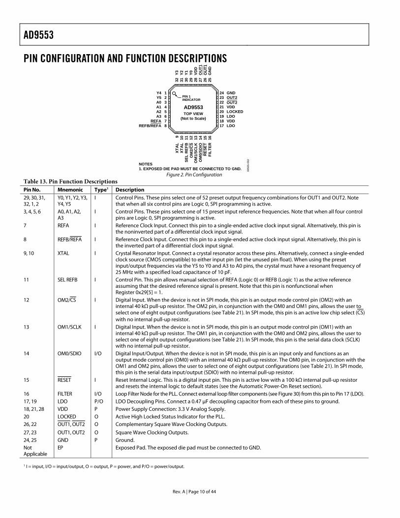
PIN CONFIGURATION AND FUNCTION DESCRIPTIONS
NOTES1. EXPOSED DIE PAD MUST BE CONNECTED TO GND.
PIN 1INDICATOR
1Y42Y53A04A15A26A37REFA8REFB/REFA
24 GND23 OUT22221 VDD20 LOCKED19 LDO18 VDD17 LDO
9X
TA
L10
XT
AL
11S
EL
RE
FB
12 13O
M1/
SC
LK
14O
M0/
SD
IO15
RE
SE
T16
FIL
TE
R
32Y
331
Y2
30Y
129
Y0
28V
DD
27O
UT
126 25
GN
D
TOP VIEW(Not to Scale)
AD9553
OU
T1
OUT2
OM
2/C
S
085
65-0
02
Figure 2. Pin Configuration
Table 13. Pin Function Descriptions Pin No. Mnemonic Type1 Description 29, 30, 31, 32, 1, 2
Y0, Y1, Y2, Y3, Y4, Y5
I Control Pins. These pins select one of 52 preset output frequency combinations for OUT1 and OUT2. Note that when all six control pins are Logic 0, SPI programming is active.
3, 4, 5, 6 A0, A1, A2, A3
I Control Pins. These pins select one of 15 preset input reference frequencies. Note that when all four control pins are Logic 0, SPI programming is active.
7 REFA I Reference Clock Input. Connect this pin to a single-ended active clock input signal. Alternatively, this pin is the noninverted part of a differential clock input signal.
8 REFB/REFA I Reference Clock Input. Connect this pin to a single-ended active clock input signal. Alternatively, this pin is the inverted part of a differential clock input signal.
9, 10 XTAL I Crystal Resonator Input. Connect a crystal resonator across these pins. Alternatively, connect a single-ended clock source (CMOS compatible) to either input pin (let the unused pin float). When using the preset input/output frequencies via the Y5 to Y0 and A3 to A0 pins, the crystal must have a resonant frequency of 25 MHz with a specified load capacitance of 10 pF.
11 SEL REFB I Control Pin. This pin allows manual selection of REFA (Logic 0) or REFB (Logic 1) as the active reference assuming that the desired reference signal is present. Note that this pin is nonfunctional when Register 0x29[5] = 1.
12 OM2/CS I Digital Input. When the device is not in SPI mode, this pin is an output mode control pin (OM2) with an internal 40 kΩ pull-up resistor. The OM2 pin, in conjunction with the OM0 and OM1 pins, allows the user to select one of eight output configurations (see Table 21). In SPI mode, this pin is an active low chip select (CS) with no internal pull-up resistor.
13 OM1/SCLK I Digital Input. When the device is not in SPI mode, this pin is an output mode control pin (OM1) with an internal 40 kΩ pull-up resistor. The OM1 pin, in conjunction with the OM0 and OM2 pins, allows the user to select one of eight output configurations (see Table 21). In SPI mode, this pin is the serial data clock (SCLK) with no internal pull-up resistor.
14 OM0/SDIO I/O Digital Input/Output. When the device is not in SPI mode, this pin is an input only and functions as an output mode control pin (OM0) with an internal 40 kΩ pull-up resistor. The OM0 pin, in conjunction with the OM1 and OM2 pins, allows the user to select one of eight output configurations (see Table 21). In SPI mode, this pin is the serial data input/output (SDIO) with no internal pull-up resistor.
15 RESET I Reset Internal Logic. This is a digital input pin. This pin is active low with a 100 kΩ internal pull-up resistor and resets the internal logic to default states (see the Automatic Power-On Reset section).
16 FILTER I/O Loop Filter Node for the PLL. Connect external loop filter components (see Figure 30) from this pin to Pin 17 (LDO). 17, 19 LDO P/O LDO Decoupling Pins. Connect a 0.47 μF decoupling capacitor from each of these pins to ground. 18, 21, 28 VDD P Power Supply Connection: 3.3 V Analog Supply. 20 LOCKED O Active High Locked Status Indicator for the PLL. 26, 22 OUT1, OUT2 O Complementary Square Wave Clocking Outputs.
27, 23 OUT1, OUT2 O Square Wave Clocking Outputs. 24, 25 GND P Ground. Not Applicable
EP Exposed Pad. The exposed die pad must be connected to GND.
1 I = input, I/O = input/output, O = output, P = power, and P/O = power/output.

AD9553
Rev. A | Page 11 of 44
TYPICAL PERFORMANCE CHARACTERISTICS –30
–40
–50
–60
–70
–80
–90
–100
–110
–120
–130
–140
–150
–16010 100 1k 10k 100k 1M 10M 100M
PHA
SE N
OIS
E (d
Bc/
Hz)
FREQUENCY OFFSET FROM CARRIER (Hz)
JITTER BANDWIDTH12kHz TO 20MHz50kHz TO 80MHz
JITTER (rms)1.30ps0.62ps
0856
5-20
3
Figure 3. Phase Noise, Pin Programmed
(fXTAL = 25 MHz, fOUT1 = 156.25 MHz)
–30
–40
–50
–60
–70
–80
–90
–100
–110
–120
–130
–140
–150
–16010 100 1k 100k10k
PHA
SE N
OIS
E (d
Bc/
Hz)
FREQUENCY OFFSET FROM CARRIER (Hz)
JITTER BANDWIDTH12kHz TO 20MHz50kHz TO 80MHz
JITTER (rms)0.89ps0.58ps
0856
5-30
41M 10M 100M
Figure 4. Phase Noise, Pin Programmed
(fREF = 25 MHz, fOUT1 = 125 MHz, Pin Ax = 1110)
–30
–40
–50
–60
–70
–80
–90
–100
–110
–120
–130
–140
–150
–16010 100 1k 10k 100k 1M 10M 100M
PHA
SE N
OIS
E (d
Bc/
Hz)
FREQUENCY OFFSET FROM CARRIER (Hz)
JITTER BANDWIDTH12kHz TO 20MHz50kHz TO 80MHz
JITTER (rms)1.25ps0.63ps
0856
5-20
4
Figure 5. Phase Noise, Pin Programmed
(fREF = 61.44 MHz, fOUT1 = 122.88 MHz)
–70
–80
–90
–100
–110
–120
–130
–140
–150
–160100 1k 10k 100k 1M 10M 100M
PHA
SE N
OIS
E (d
Bc/
Hz)
FREQUENCY OFFSET FROM CARRIER (Hz)
JITTER BANDWIDTH12kHz TO 20MHz50kHz TO 80MHz
JITTER (rms)0.73ps0.51ps
0856
5-20
5
Figure 6. Phase Noise, Pin Programmed
(fREF = 77.76 MHz, fOUT1 = 622.08 MHz)
–30
–40
–50
–60
–70
–80
–90
–100
–110
–120
–130
–140
–150
–16010 100 1k 10k 100k 1M 10M 100M
PHA
SE N
OIS
E (d
Bc/
Hz)
FREQUENCY OFFSET FROM CARRIER (Hz)
JITTER BANDWIDTH12kHz TO 20MHz50kHz TO 80MHz
JITTER (rms)1.26ps0.49ps
0856
5-20
6
Figure 7. Phase Noise, Pin Programmed
(fREF = 19.44 MHz, fOUT1 = 155.52 MHz)
–30
–40
–50
–60
–70
–80
–90
–100
–110
–120
–130
–140
–150
–16010 100 1k 10k 100k 1M 10M 100M
PHA
SE N
OIS
E (d
Bc/
Hz)
FREQUENCY OFFSET FROM CARRIER (Hz)
JITTER BANDWIDTH12kHz TO 20MHz50kHz TO 80MHz
JITTER (rms)1.27ps0.54ps
0856
5-20
7
Figure 8. Phase Noise, Pin Programmed
(fREF = 8 kHz, fOUT1 = 155.52 MHz)

AD9553
Rev. A | Page 12 of 44
5
–30
–25
–20
–15
–10
–5
0
10 1k100
MA
GN
ITU
DE
(dB
)
FREQUENCY OFFSET (Hz) 0856
5-02
8
JITTER TRANSFER
MA
GN
ITU
DE
(dB
)
FREQUENCY OFFSET (Hz)
2
1
0
–1
–2
–30 25 50 75 100 125 150 175
JITTER PEAKING
Figure 9. Jitter Transfer, Loop Bandwidth = 170 Hz
10
–60
–50
–40
–30
–20
–10
0
1k 10k 100k 1M
MA
GN
ITU
DE
(dB
)
FREQUENCY OFFSET (Hz) 0856
5-31
1
JITTER TRANSFER
Figure 10. Jitter Transfer, Loop Bandwidth = 20 kHz
5
–45
–25
–40
–35
–30
–20
–15
–10
–5
0
10 1k100
MA
GN
ITU
DE
(dB
)
FREQUENCY OFFSET (kHz) 0856
5-02
9
JITTER TRANSFER
MA
GN
ITU
DE
(dB
)
FREQUENCY OFFSET (kHz)
1
0
–1
–2
–310 20 30 40 50 60 70 80
JITTER PEAKING
Figure 11. Jitter Transfer, Loop Bandwidth = 75 kHz
242
243
244
245
246
247
248
249
TIME (ms)
FREQ
UEN
CY
(MH
z)
0 2 4 6 8 10 12 14 16 18 20
REF B TO ATRANSITION
REF A TO BTRANSITION
248.3MHz
242.8MHz
REF A TO XTALTRANSITION
XTAL TO REF ATRANSITION
–19.6MHz/ms
+15.6MHz/ms
0856
5-31
3
Figure 12. Output Transient Due to Input Reference Switchover,
Pin Ax = 0110, Pin Yx = 000001, Loop Bandwidth = 170 Hz
654
656
658
660
662
664
666
0 5 10 15 20 25 30 35 40 45 50
TIME (µs)
FREQ
UEN
CY
(MH
z)
REF A TO BTRANSITION
REF B TO ATRANSITION
–13.6MHz/µs–15.2MHz/µs
655.20 MHz655.24 MHz
0856
5-31
4
Figure 13. Output Transient Due to Input Reference Switchover,
Pin Ax = 1101, Pin Yx = 101101, Loop Bandwidth = 75 kHz
0856
5-31
5
612
614
616
618
620
622
624
0 5 10 15 20 25 30 35 40 45 50
TIME (µs)
FREQ
UEN
CY
(MH
z)
REF B TO ATRANSITION
REF A TO BTRANSITION
–15.2MHz/µs
614.09MHz613.31MHz
–10.4MHz/µs
Figure 14. Output Transient Due to Input Reference Switchover,
Pin Ax = 1110, Pin Yx = 110011, Loop Bandwidth = 75 kHz
AD9553
Rev. A | Page 13 of 44
35
0
5
10
15
20
25
30
0 900800700600500400300200100
SUPP
LY C
UR
REN
T (m
A)
FREQUENCY (MHz)
LVPECL
LVDS WEAK
LVDS STRONG
0856
5-20
9
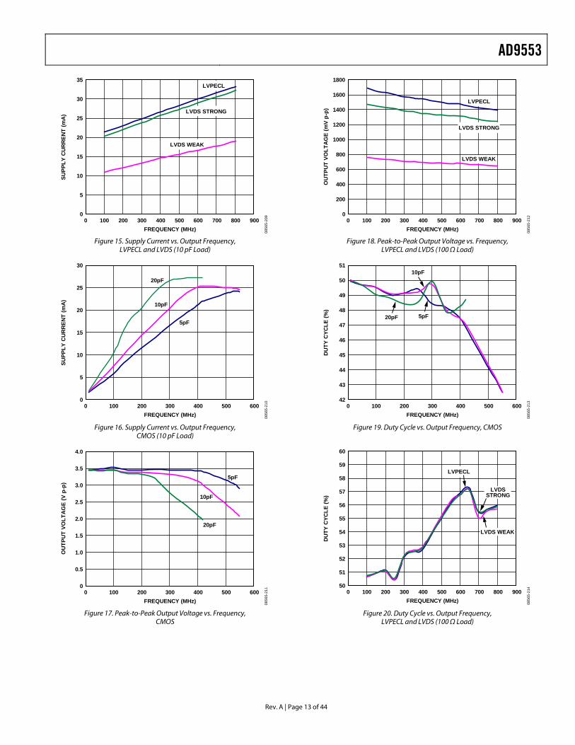
Figure 15. Supply Current vs. Output Frequency,
LVPECL and LVDS (10 pF Load)
0
5
10
15
20
25
30
0 600500400300200100
SUPP
LY C
UR
REN
T (m
A)
FREQUENCY (MHz)
10pF
20pF
5pF
0856
5-21
0
Figure 16. Supply Current vs. Output Frequency,
CMOS (10 pF Load)
0
0.5
1.0
1.5
2.0
2.5
4.0
3.0
3.5
0 600500400300200100
OU
TPU
T VO
LTA
GE
(V p
-p)
FREQUENCY (MHz)
10pF
20pF
5pF
0856
5-21
1
Figure 17. Peak-to-Peak Output Voltage vs. Frequency,
CMOS
0
200
400
600
800
1000
1800
1600
1200
1400
OU
TPU
T VO
LTA
GE
(mV
p-p)
0 900800700600500400300200100FREQUENCY (MHz)
LVPECL
LVDS STRONG
LVDS WEAK
0856
5-21
2
Figure 18. Peak-to-Peak Output Voltage vs. Frequency,
LVPECL and LVDS (100 Ω Load)
42
51
50
49
48
47
46
45
44
43
0 600500400300200100
DU
TY C
YCLE
(%)
FREQUENCY (MHz)
10pF
20pF 5pF
0856
5-21
3
Figure 19. Duty Cycle vs. Output Frequency, CMOS
50
51
52
53
54
55
56
57
58
59
60
0 900800700600500400300200100
DU
TY C
YCLE
(%)
FREQUENCY (MHz)
LVPECL
LVDS WEAK
LVDSSTRONG
0856
5-21
4
Figure 20. Duty Cycle vs. Output Frequency,
LVPECL and LVDS (100 Ω Load)

AD9553
Rev. A | Page 14 of 44
2
200mV/DIV 500ps/DIV
085
65-2
15
Figure 21. Typical Output Waveform, LVPECL (800 MHz)
2
125mV/DIV 500ps/DIV
085
65-2
16
Figure 22. Typical Output Waveform, LVDS (800 MHz, 3.5 mA Drive Current)
2
500mV/DIV 1.25ns/DIV
085
65-2
17
Figure 23. Typical Output Waveform, CMOS (250 MHz, 10 pF Load)

AD9553
Rev. A | Page 15 of 44
INPUT/OUTPUT TERMINATION RECOMMENDATIONS
AD9553
100Ω
HIGHIMPEDANCE
INPUTDOWNSTREAM
DEVICE
0.1µF
0.1µF
3.3V DIFFERENTIALOUTPUT
(LVDS ORLVPECL MODE)
0856
5-32
4
Figure 24. AC-Coupled LVDS or LVPECL Output Driver
AD9553
100Ω DOWNSTREAM
DEVICE3.3V DIFFERENTIALOUTPUT
(LVDS ORLVPECL MODE)
0856
5-32
5
Figure 25. DC-Coupled LVDS or LVPECL Output Driver
0.1µF
0.1µF
AD9553SELF-BIASEDREFERENCE
INPUT(OPT
ION
AL)
100Ω
0856
5-32
6
Figure 26. Reference Input

AD9553
Rev. A | Page 16 of 44
THEORY OF OPERATION
A[3:0]
REGISTER BANK OUTPUT MODE/SERIAL PORT
PRECONFIGUREDDIVIDER SETTINGS
REFA
XTAL
Y[5:0]
4
6
3
XTAL
VCO
AD9553
OUT1
3350MHzTO
4050MHz
LOCKED FILTER
2
N
PFD
OUT22
20
3 10
10
P0 P1
P2
P2
P0 P1
DN
UP
33
SPI CTRL
3
×2
FDBK
REFERENCESWITCHOVER
CONTROL
CLOCKMUX
CLOCK MUX
HOLD
HOLD
REFSEL
DETA
DETB
DETXO
SEL REFB
DCXOCTRL
TEST
1 0
01
01
01
RA, ×2A, ÷5ARB, ×2B, ÷5B
RXO, DCXO CTRLN, P0, P1, P2
REF SELTEST
REF DIFF
REFDIFF
÷501
÷5A
÷501
÷5B
REFB/REFA
XO
FPFD
PLL
14
DETDET A
01 ÷RA
÷N
×2A RA
×2
14
DETDET B
01 ÷RB
×2B RB
×2
14
DETDET XO
÷RXO
RXO
TUNINGCONTROL
UP/2FPFD/2FDBK/2
XO LOCKDETECT
OUTPUTMODE
CONTROL
5 TO 11LOOP
FILTERCHARGE
PUMP
0856
5-10
1
Figure 27. Detailed Block Diagram
OVERVIEW The AD9553 can receive up to two input reference clocks, REFA and REFB. Both input clock paths include an optional divide-by-5 (÷5) prescaler, an optional ×2 frequency multiplier, and a 14-bit programmable divider. Alternatively, the user can program the device to operate with one differential input clock (instead of two single-ended input clocks) via the serial I/O port. In the differential operating mode, the REFB path is inactive.
The AD9553 also has a dedicated XTAL input for direct connec-tion of an optional 25 MHz crystal resonator. This allows for a backup clock signal useful for holdover operation in case both input references fail. The XTAL clock path includes a fixed ×2 frequency multiplier and a 14-bit programmable divider.
The AD9553 includes a switchover control block that auto-matically handles switching from REFA to REFB (or vice versa) in the event of a reference failure. If both REFA and REFB fail, however, then the switchover control block automatically enters holdover mode by selecting the XTAL clock signal (assuming the presence of a crystal resonator at the XTAL input).
Generally, the clock signals that appear at the input to the clock multiplexer (see Figure 27) all operate at the same frequency. Thus, the frequency at the input to the PLL (FPFD in Figure 27) is the same regardless of the signal selected by the clock multi-plexer. The PLL converts FPFD to a frequency within the operating range of the VCO (3.35 GHz to 4.05 GHz) based on the value of the feedback divider (N). The VCO prescaler (P0) reduces the VCO output frequency by an integer factor of 5 to 11, resulting in an intermediate frequency in the range of 305 MHz to 810 MHz.
The 10-bit P1 and P2 dividers can further reduce the P0 output frequency to yield the final output clock frequencies at OUT1 and OUT2, respectively.
Thus, the frequency translation ratio from the reference input to the output depends on the selection of the ÷5 prescalers; the ×2 frequency multipliers; the values of the three R dividers; the N divider; and the P0, P1, and P2 dividers. These parameters are set automatically via the preconfigured divider settings per the Ax and Yx pins (see the Preset Frequencies section). Alternatively, the user can custom program these parameters via the serial I/O port (see the Serial Control Port and Register Map sections), which allows the device to accommodate custom frequency translation ratios.
PRESET FREQUENCIES The frequency selection pins (A3 to A0 and Y5 to Y0) allow the user to hardwire the device for preset input and output frequencies based on the pin logic states (see Figure 27). The pins decode ground or open connections as Logic 0 or Logic 1, respectively.
To have access to the device control registers via the SPI port, the user must select Pin Y5 to Pin Y0 = 000000 and/or Pin A3 to Pin A0 = 0000. Doing so causes Pin 12 through Pin 14 to function as SPI port control pins instead of output mode control pins (see the Output Driver Mode Control section). Note that after selecting SPI mode, the user must write a Logic 1 to Bit 0 of Register 0x32 and Register 0x34 to enable the registers as the source of the OUT1 and OUT2 mode control bits (see Figure 31 and the Output Driver Mode Control section).

AD9553
Rev. A | Page 17 of 44
The Ax pins allow the user to select one of fifteen input reference frequencies as shown in Table 14. The device sets the appropriate divide-by-5 (÷5A, ÷5B), multiply-by-2 (×2A, ×2B), and input divider (RA, RB, RXO) values based on the logic levels applied to the Ax pins.
The same settings apply to both the REFA and REFB input paths. Furthermore, the ÷5, ×2, and R values cause the PLL input frequency to be either 16 kHz or 40/3 kHz. There are two exceptions. The first is for Pin A3 to Pin A0 = 1101, which yields a PLL input frequency of 155.52/59 MHz. The second is for Pin A3 to Pin A0 = 1110, which yields a PLL input frequency of either 1.5625 MHz or 4.86 MHz depending on the Yx pins.
Note that the XTAL input is not available for holdover func-tionality in the A3 to A0 = 1101 and 1110 pin configurations, thus the undefined RXO value.
The Yx pins allow the user to select one of 52 output frequency combinations (fOUT1 and fOUT2) per Table 15. The device sets the appropriate P0, P1, and P2 settings based on the logic levels applied to the Yx pins. Note, however, that selections 101101 through 110010 require Pin A3 to Pin A0 = 1101, and selection 110011 requires Pin A3 to Pin A0 = 1110.
The value (N) of the PLL feedback divider and the control setting for the charge pump current (CP) depend on a combi-nation of both the Ax and Yx pin settings as shown in Table 16.
Table 14. Pin Configured Input Frequency, Ax Pins1
Pin A3 to Pin A0 fREFA, fREFB (MHz) Divide-by-5A, Divide-by-5B ×2A, ×2B RA, RB (Decimal) RXO (Decimal)
0000 SPI mode 0001 0.008 Bypassed On 1 3125 0010 1.536 Bypassed Bypassed 96 3125 0011 2.048 Bypassed Bypassed 128 3125 0100 16.384 Bypassed Bypassed 1024 3125 0101 19.44 Bypassed Bypassed 1215 3125 01102 25 Bypassed On 3125 3125 0111 38.88 Bypassed Bypassed 2430 3125 1000 61.44 Bypassed Bypassed 3840 3125 1001 77.76 Bypassed Bypassed 4860 3125 1010 122.88 Bypassed Bypassed 7680 3125 1011 125 On On 3125 3125 1100 1.544 Bypassed On 193 3125
11013 155.52 Bypassed Bypassed 59 Undefined
11104 25 or 77.76 Bypassed Bypassed 16 Undefined 1111 200/3 Bypassed Bypassed 5000 3750 1 For divide-by-5 and ×2 frequency scalers, “On” indicates active. 2 Using A0 to A3 = 0110 to yield a 25 MHz to 125 MHz conversion provides a loop bandwidth of 170 Hz. An alternate 25 MHz to 125 MHz conversion uses A0 to A3 = 1110, which
provides a loop bandwidth of 20 kHz. 3 Pin A3 to Pin A0 = 1101 only works with Pin Y5 to Pin Y0 =101101 through 110010. 4 Pin A3 to Pin A0 = 1110 only works with Pin Y5 to Pin Y0 =110011 or 111111.

AD9553
Rev. A | Page 18 of 44
Table 15. Pin Configured Output Frequency, Yx Pins Pin Y5 to Pin Y0 fVCO (MHz) fOUT1 (MHz) fOUT2 (MHz) P0 P1 P2
000000 SPI mode
000001 3686.4 245.76 245.76 5 3 3 000010 3686.4 245.76 122.88 5 3 6 000011 3686.4 245.76 61.44 5 3 12 000100 3686.4 245.76 16.384 5 3 45 000101 3686.4 245.76 2.048 5 3 360 000110 3686.4 245.76 1.536 5 3 480 000111 3686.4 122.88 122.88 5 6 6 001000 3686.4 122.88 61.44 5 6 12 001001 3686.4 122.88 16.384 5 6 45 001010 3686.4 122.88 2.048 5 6 360 001011 3686.4 122.88 1.536 5 6 480 001100 3686.4 61.44 61.44 5 12 12 001101 3686.4 61.44 16.384 5 12 45 001110 3686.4 61.44 2.048 5 12 360 001111 3686.4 61.44 1.536 5 12 480 010000 3686.4 16.384 16.384 5 45 45 010001 3686.4 16.384 2.048 5 45 360 010010 3686.4 16.384 1.536 5 45 480 010011 3686.4 2.048 2.048 5 360 360 010100 3686.4 2.048 1.536 5 360 480 010101 3686.4 1.536 1.536 5 480 480 010110 3750 156.25 156.25 6 4 4 010111 3750 156.25 125 6 4 5 011000 3750 156.25 25 6 4 25 011001 3750 125 125 6 5 5 011010 3750 125 25 6 5 25 011011 3750 25 25 6 25 25 011100 3732.48 155.52 155.52 6 4 4 011101 3732.48 155.52 77.76 6 4 8 011110 3732.48 155.52 19.44 6 4 32 011111 3732.48 77.76 77.76 6 8 8 100000 3732.48 77.76 19.44 6 8 32 100001 3732.48 19.44 19.44 6 32 32 100010 3686.4 153.6 153.6 6 4 4 100011 3686.4 153.6 122.88 6 4 5 100100 3686.4 153.6 61.44 6 4 10 100101 3686.4 153.6 2.048 6 4 300 100110 3686.4 153.6 1.536 6 4 400 100111 3600 100 100 6 6 6 101000 3600 100 50 6 6 12 101001 3600 100 25 6 6 24 101010 3600 50 50 6 12 12 101011 3600 50 25 6 12 24 101100 3705.6 1.544 1.544 6 400 400 101101 ~3985.53 fO
1 fO1 6 1 1
101110 ~3985.53 fO1 fO/21 6 1 2
101111 ~3985.53 fO1 fO/41 6 1 4
110000 ~3985.53 fO/21 fO/21 6 2 2 110001 ~3985.53 fO/21 fO/41 6 2 4 110010 ~3985.53 fO/41 fO/41 6 4 4 110011 3732.48 622.08 622.08 6 1 1 110100 to 111110 Undefined Undefined Undefined Undefined Undefined Undefined 111111 3750 125 25 5 6 30 1 fO = 39,191.04/59 MHz.

AD9553
Rev. A | Page 19 of 44
Table 16. Pin Configuration vs. PLL Feedback Divider (N) and Charge Pump Value (CP) A3 to A0 Y5 to Y0 N1 CP2
0001 to 1100 000001 to 010101 230,400 121 010110 to 011011 234,375 121 011100 to 100001 233,280 121 100010 to 100110 230,400 121 100111 to 101011 225,000 121 101100 231,600 121 101101 to 111111 Undefined Undefined 1101 000001 to 101100 Undefined Undefined 101101 to 110010 1512 255 110010 to 111111 Undefined Undefined 1110 000001 to 110010 Undefined Undefined 110011 768 121 110100 to 111110 Undefined Undefined 111111 2400 121 1111 000001 to 010101 276,480 145 010110 to 011011 281,250 145 011100 to 100001 279,936 145 100010 to 100110 276,480 145 100111 to 101011 270,000 145 101100 277,920 145 101101 to 111111 Undefined Undefined 1 PLL feedback divider value (decimal). 2 Charge pump register value (decimal). Multiply by 3.5 µA to yield ICP.
DEVICE CONTROL MODES The AD9553 provides two modes of control: pin control and register control. Pin control, via the frequency selection pins (Ax and Yx) as described in the Preset Frequencies section, is the simplest. Typically, pin control is for applications requiring only a single set of operating parameters (assuming that one of the options available via the frequency selection pins provides the parameters that satisfy the application requirements). Register control is typically for applications that require the flexibility to program different operating parameters from time to time, or for applications that require parameters not available with any of the pin control options. The block diagram (see Figure 28) shows how the SPI and pin control modes interact.
The SPI/OM[2:0] label in Figure 28 refers to Pin 12, Pin 13, and Pin 14 of the AD9553. Furthermore, the SPI mode signal is Logic 1 when Pin A3 to Pin A0 = 0000 and/or Pin Y5 to Pin Y0 = 000000; otherwise, it is Logic 0. The SPI/OM[2:0] pins serve double duty (as either SPI pins or output mode control pins). A mux (controlled by the SPI mode signal) selects whether the three signals associated with the SPI/OM[2:0] pins connect to the output mode control decoder or to the SPI controller. Note that the SPI mode signal originates from the frequency selec-tion pins decoder.
To enable communication with the SPI controller (SPI mode), the user must apply the appropriate logic pattern to the frequency selection pins (A3 to A0 = 0000 and/or Y5 to Y0 = 000000).
Note that as long as the frequency selection pins are set to invoke SPI mode, the user cannot establish output mode control via the output mode control decoder. Conversely, when the frequency selection pins are set to anything other than SPI mode, the user cannot communicate with the device via the SPI controller.
In Figure 28, note that some of the functions internal to the AD9553 are controlled by function bits that originate either from the two pin decoders or from within the register map. Specifically, each function receives its function bits from a function mux; and each function mux, in turn, receives its control signal from a single enable SPI control bit in the register map.
Be aware that the default values within the register map are such that all enable SPI control bits are Logic 0. Thus, the default state of the device is such that each function mux selects the pin decoders (not the register map) as the source for all control functions.
In order to switch a function mux so that it selects function bits from the register map, the user must first set the frequency selec-tion pins to SPI mode. Then, write a Logic 1 to the appropriate enable SPI control bit in the register map. Be aware that the function mux routes the function bits in the register map to the selected function the instant that the enable SPI control bit becomes Logic 1. Thus, it is a good idea to program the function bits to the desired state prior to writing Logic 1 to the corresponding enable SPI control bit.

AD9553
Rev. A | Page 20 of 44
A[3:0]
4
SPI/OM[2:0]
3
0
1
1 0
3
0
1
FUNCTIONABC BITS
0
1
FUNCTIONXYZ BITS
ENABLE SPI CONTROLOF OUTPUT MODE
ENABLE SPI CONTROLOF OUTPUT ABC BITS
ENABLE SPI CONTROLOF FUNCTIONING XYZ
OUTPUTMODE
CONTROLFUNCTION
BITS
REGISTER MAPFUNCTION
MUXES
SPI CONTROLLER
FREQUENCYSELECTION
PINS DECODER
OUTPUTMODE
CONTROLDECODER
OUTPUT MODECONTROLFUNCTION
FUNCTIONABC
FUNCTIONXYZ
Y[5:0]
6
3 3
3
SPI MODE
0856
5-10
0
Figure 28. Control Mode Diagram
Although the SPI and pin control modes are functionally independent, it is possible to mix the control modes. For example, suppose that pin control satisfies all of the require-ments for an application except for the value of the P2 divider (which is associated with OUT2). The user could do the following:
• Activate SPI mode via the frequency selection pins. • Program the desired P0, P1, and P2 values in the register
map (Register 0x15 to Register 0x18). • Set the enable SPI control bit for the output dividers
(Register 0x14[2] = 1). • Calibrate the VCO by enabling SPI control of VCO
calibration (Register 0x0E[2] = 1), then issue a calibrate command (Register 0x0E[7] = 1). Be sure to program the N divider, R dividers, ÷5 dividers, and ×2 multipliers to the values defined by the Ax and Yx pin settings prior to cali-brating the VCO.
• Restore the original settings to the frequency selection pins to invoke the desired frequency selection.
In this way, the function muxes that control P0, P1, and P2 select the appropriate register bits as the source for controlling the dividers, while all the other function muxes select the pin decoders as the source for controlling the other functions. Note that the dividers remain under register control until the user activates
SPI mode and writes Register 0x14[2] = 0, thereby causing the function mux to use the frequency selection pins decoder as the source for controlling the dividers, instead of the register map.
DESCRIPTION OF FUNCTIONAL BLOCKS Reference Inputs
The default configuration of the AD9553 provides up to two single-ended input clock receivers, REFA and REFB, which are high impedance CMOS inputs. In applications that require redun-dant reference clocks with switchover capability, REFA is the primary reference and REFB the secondary reference. Alternatively, the user can configure the input (via the serial I/O port) as a single differential receiver. In this case, the REFB input func-tions as REFA (the complementary input of REFA). Note that in this configuration the device operates with only one reference input clock, eliminating the need for switchover functionality.
XTAL Input
The AD9553 accepts an optional 25 MHz crystal resonator connected across the XTAL pins. Alternatively, it accepts a single-ended clock source (CMOS compatible) connected to either one of the XTAL input pins (in this case, the unused input remains floating). Unless otherwise programmed, the device expects the crystal to have a specified load capacitance of 10 pF (default). The AD9553 provides the necessary load capacitance internally. The internal load capacitance consists

AD9553
Rev. A | Page 21 of 44
of a fixed component of 8 pF and a variable (programmable) component of 0 pF to 15.75 pF.
After applying power to the AD9553 (or after a device reset), the programmable component defaults to 2 pF. This establishes the default load capacitance of 10 pF (8 pF fixed plus 2 pF programmable).
To accommodate crystals with a specified load capacitance other than 10 pF (8 pF to 23.75 pF), the user can adjust the program-mable capacitance in 0.25 pF increments via Register 0x1B[5:0]. Note that when the user sets Register 0x1B[7] to 0 (enabling SPI control of the XTAL tuning capacitors), the variable capacitance changes from 2 pF (its default power-up value) to 15.75 pF due to the default value of Register 0x1B[5:0]. This causes the crystal load capacitance to be 23.75 pF until the user overwrites the default contents of Register 0x1B[5:0].
A noncomprehensive, alphabetical list of crystal manufacturers includes the following:
• AVX/Kyocera • ECS • Epson Toyocom • Fox Electronics • NDK • Siward
Although these crystals meet the load capacitance and motional resistance requirements of the AD9553 according to their data sheets, Analog Devices, Inc., does not guarantee their operation with the AD9553, nor does Analog Devices endorse one supplier of crystals over another.
Input Frequency Prescalers (Divide-by-5A, Divide-by-5B)
The divide-by-5 prescalers provide the option to reduce the input reference frequency by a factor of five. Note that the prescalers physically precede the ×2 frequency multipliers. This allows the prescalers to bring a high frequency reference clock down to a frequency that is within the range of the ×2 frequency multipliers.
Input ×2 Frequency Multipliers (×2A, ×2B)
The ×2 frequency multipliers provide the option to double the frequency at their input; thereby taking advantage of a higher frequency at the input to the PLL (FPFD). This provides greater separation between the frequency generated by the PLL and the modulation spur associated with the frequency at the PLL input. However, increased reference spur separation comes at the expense of the harmonic spurs introduced by the frequency multiplier. As such, beneficial use of the frequency multiplier is application specific. Note that the maximum input frequency to the ×2 fre-quency multipliers must not exceed 125 MHz.
Input Clock Detectors
The three clock input sections (REFA, REFB, and XTAL) include a dedicated monitor circuit that detects signal presence at the input. The detectors provide input to the switchover control block to support automatic reference switching and holdover operation.
Switchover/Holdover
The AD9553 supports automatic reference switching and hold-over functions. It also supports manual reference switching via an external pin (SEL REFB) or via program control using the serial I/O port. A block diagram of the switchover/holdover capability appears in Figure 29. Note that the mux selects one of the three input signals (REFA, REFB, or XTAL) routing it to the input of the PLL. The selection of an input signal depends on which signals are present along with the contents of Register 0x29[7:6] and the logic level at the SEL REFB pin.
Note that each input signal has a dedicated signal presence detector. Each detector uses the feedback signal from the PLL as a sampling clock (which is always present due to the free-running VCO). This allows the detectors to determine the presence or absence of the input signals reliably. Note that the mux control logic uses the detector signals directly in order to determine the need for a switch to holdover operation.
Holdover occurs whenever the mux control logic determines that both the REFA and REFB signals are not present, in which case the device selects the XTAL signal if it is present. The excep-tion is when Register 0x29[7:6] = 10 or 11, which disables the holdover function. If none of the three input signals is present, the device waits until at least one signal becomes present and selects according to the device settings (Register 0x29[7:6] and the logic level at the SEL REFB pin).
When the device is reset (or following a power-up), the internal logic defaults to revertive switchover mode (Register 0x29[7:6] = 00). In revertive switchover mode, the device selects the REFA signal whenever it is present. If REFA is not present, then the device selects the REFB signal, if present, but returns to REFA whenever it becomes available. That is, in revertive switchover mode, the device favors REFA. If both REFA and REFB are not present, the device switches to holdover mode.
When programmed for nonrevertive switchover mode (Register 0x29[7:6] = 01), the device selects the REFA signal if it is present. If REFA is not present, then the device selects the REFB signal (if present). Even if REFA becomes available, the device continues to use REFB until REFB fails. That is, in nonrevertive switchover mode, the switch to REFB is permanent unless REFB fails (or unless both REFA and REFB fail, in which case the device switches to holdover mode).

AD9553
Rev. A | Page 22 of 44
00
11
10
01
REG 0x29[7:6]
REVERTIVE
NON-REVERTIVE
SELECT REFA
SELECT REFB
REVERTIVE/NON-REVERTIVE
LOGIC
SPI SELECT REFA/BLOGIC
SELREFB
FROM REFAINPUT
FROM REFBINPUT
FROM XTALINPUT
SIGNAL
DETECTOR REFA PRESENT
REFB PRESENT
XTAL PRESENT
REFA/BSELECTION LOGIC
MUXCONTROL
LOGIC
TOPLL
SEL B/ASEL B/A
SEL B/A
SEL B/A
11
FDBK
CLOCKMUX
RA DIVIDER
÷
÷
÷
RB DIVIDER
RXO DIVIDER
0856
5-10
2
Figure 29. Switchover/Holdover Block Diagram
The user can override the automatic switchover functions (revertive and nonrevertive) and manually select the REFA or REFB signal by programming Register 0x29[7:6] = 10 or 11, respectively. Note, however, that the desired signal (REFA or REFB) must be present for the device to select it.
The user can also force the device to switch to REFB by applying a Logic 1 to the external SEL REFB pin. This overrides a REFA selection invoked by either the revertive/nonrevertive logic or when Register 0x29[7:6] = 10. Note, however, that REFB must be present to be selected by the device.
PLL (PFD, Charge Pump, VCO, Feedback Divider)
The PLL (see Figure 27) consists of a phase/frequency detector (PFD), a partially integrated analog loop filter (see Figure 30), an integrated voltage controlled oscillator (VCO), and a 20-bit programmable feedback divider. The PLL generates a 3.35 GHz to 4.05 GHz clock signal that is phase locked to the active input reference signal, and its frequency is the phase detector frequency (FPFD) multiplied by the feedback divider value (N).
The PFD of the PLL drives a charge pump that increases, decreases, or holds constant the charge stored on the loop filter capacitors (both internal and external). The stored charge results in a voltage that sets the output frequency of the VCO. The feedback loop of the PLL causes the VCO control voltage to vary in such a way as to phase lock the PFD input signals. Note that the PFD supports input frequencies spanning 13.3 kHz to 100 MHz (implying that input frequencies between 8 kHz and 13.3 kHz must use the ×2 frequency multiplier in the input path).
The PLL has a VCO with 128 frequency bands spanning a range of 3350 MHz to 4050 MHz (3700 MHz nominal). However, the actual operating frequency within a particular band depends on the control voltage that appears on the loop filter capacitor. The control voltage causes the VCO output frequency to vary linearly within the selected band. This frequency variability allows the control loop of the PLL to synchronize the VCO output signal with the reference signal applied to the PFD.
Typically, selection of the VCO frequency band (as well as gain adjustment) occurs automatically as part of the automatic VCO calibration process of the device, which initiates at power up (or reset). Alternatively, the user can force VCO calibration by first enabling SPI control of VCO calibration (Register 0x0E[2] = 1) and then writing a 1 to the calibrate VCO bit (Register 0x0E[7]). Note that VCO calibration centers the dc operating point of the VCO control signal. Furthermore, during VCO calibration, the output drivers provide a static dc signal.
To facilitate system debugging, the user can override the VCO band setting by first enabling SPI control of VCO band (Register 0x0E[0] = 1) and then writing the desired value to Register 0x10[7:1].
The feedback divider (N-divider) sets the frequency multi-plication factor of the PLL in integer steps over a 20-bit range. Note that the N-divider has a lower limit of 32.

AD9553
Rev. A | Page 23 of 44
Loop Filter
The charge pump in the PFD delivers current to the loop filter (see Figure 30). The components primarily responsible for the bandwidth of the loop filter are external and connect between Pin 16 and Pin 17.
The internal portion of the loop filter has two configurations: one is for low loop bandwidth applications (~170 Hz) and the other is for medium (~20 kHz)/high (~75 kHz) bandwidth applications. The low loop bandwidth condition applies when the feedback divider value (N) is 214 (16,384) or greater. Otherwise, the medium/high loop bandwidth configuration is in effect. The feedback divider value depends on the configuration of the Ax and Yx pins per Table 16.
0856
5-33
1TOVCO
3kΩ
FILTER
53pF
C1
R
AD9553
C2
375Ω
400kΩ
BUFFER170pF
CONTROLLOGIC
SWITCHES CHANGESTATE FOR N ≥ 16384
LDO1716
FROMCHARGE
PUMP
Figure 30. External Loop Filter
The bandwidth of the loop filter primarily depends on three external components (R, C1, and C2). There are two sets of recom-mended values for these components corresponding to the low and medium/high loop bandwidth configurations (see Table 17).
Table 17. External Loop Filter Components
A3 to A0 Pins R C1 C2 Loop Bandwidth
0001 to 1100, and 1111 6.8 kΩ 47 nF 1 µF 0.17 kHz 11101 12 kΩ 51 pF 220 nF 20 kHz 1101 and 11102 12 kΩ 51 pF 220 nF 75 kHz 1 The 20 kHz loop bandwidth case only applies when the A3 pin to A0 pin =
1110 and the Y5 pin to Y0 pin = 111111. 2 The 75 kHz loop bandwidth case only applies when the A3 pin to A0 pin =
1101 and the Y5 pin to Y0 pin = 101101 through 110010, or when the A3 pin to A0 pin = 1110 and the Y5 pin to Y0 pin = 110011.
To achieve the best jitter performance in applications requiring a loop bandwidth of less than 1 kHz, C1 and C2 must have an insulation resistance of at least 500 ΩF.
PLL Locked Indicator
The PLL provides a status indicator that appears at Pin 20 (LOCKED). When the PLL acquires phase lock, the LOCKED pin switches to a Logic 1 state. When the PLL loses lock, however, the LOCKED pin returns to a Logic 0 state.
Alternatively, the LOCKED pin serves as a test port allowing the user to monitor one-of-four internal clocks. Register 0x17[3:1] controls the test port as shown in Table 18.
Table 18. LOCKED Pin Output Control Register 0x17[3:1] LOCKED Pin Output 0XX PLL locked indication (default) 100 Crystal oscillator clock signal 101 PFD pump-up clock divided-by-2 110 PFD reference input clock divided-by-2 111 PLL feedback to PFD clock divided-by-2
Output Dividers
The output divider section consists of three dividers: P0, P1, and P2. The P0 divider (or VCO frequency prescaler) accepts the VCO frequency and reduces it by a factor of 5 to 11 (selectable). This brings the frequency down to a range between 305 MHz and 810 MHz.
The output of the P0 divider independently drives the P1 divider and the P2 divider. The P1 divider establishes the frequency at OUT1 and the P2 divider establishes the frequency at OUT2. The P1 and P2 dividers are each programmable over a range of 1 to 1023, which results in a frequency at OUT1 or OUT2 that is an integer submultiple of the frequency at the output of the P0 divider.
Output Driver Configuration
The user has complete control over all configurable parameters of the OUT1 and OUT2 drivers via the OUT1 and OUT2 driver control registers (Register 0x32 and Register 0x34, respectively, as shown in Figure 31). To alter the parameters from their default values, the user must use the SPI port to program the driver control registers as desired.
The OUT1 and OUT2 drivers are configurable in terms of the following parameters:
• Logic family (via mode control) • Pin function (via mode control but only applies to the
CMOS family) • Polarity (only applies to the CMOS family) • Drive current • Power-down
Output Driver Mode Control
Three mode control bits establish the logic family and pin function of the output drivers. The three bits originate either from Bits[5:3] of Register 0x32 and Register 0x34 or from the decode logic associated with the OM2 to OM0 pins as shown in Figure 31. Note that Bit 0 of Register 0x32 and Register 0x34 determines the source of the three mode control bits for the associated output driver. Specifically, when Bit 0 of the register is Logic 0 (default), the source of the mode control bits for the associated driver is the OM2 to OM0 pin decoder. When Bit 0 is Logic 1, the source of the mode control bits is from Bits[5:3] of Register 0x32 and Register 0x34.

AD9553
Rev. A | Page 24 of 44
The mode control bits establish the logic family and output pin function of the associated output driver per Table 19. The logic families include LVDS, LVPECL, and CMOS. Because both output drivers support the LVDS and LVPECL logic families, each driver has two pins to handle the differential signals associated with these two logic families. The OUT1 driver uses the OUT1 and OUT1 pins and the OUT2 driver uses the OUT2 and OUT2 pins. However, the CMOS logic family handles only single-ended signals, thereby requiring only one pin. Even though CMOS only requires one pin, both pins of OUT1 and both pins of OUT2 have a dedicated CMOS driver.
Note that the LVPECL mode of the AD9553 is not implemented using an emitter-follower topology, and therefore, a pull-down resistor is not needed (and should be avoided) on the output pins. Rather, it uses a CMOS output driver whose output amplitude and common-mode voltage are compatible with LVPECL speci-fications. 100 Ω termination across the output pair is still recommended.
The user has the option to disable (that is, tristate) either or both of the pins for OUT1 and/or OUT2 via the mode control bits (see Table 19 for the 001, 010, and 011 bit patterns). Alternatively, the user can make both pins active (see Table 19, Bit Pattern 000) to produce two single-ended CMOS output clocks at OUT1 and/or OUT2.
Table 19. Output Mode Control Bits
Mode Control Bits Logic Family Pin Function of the Output Driver
000 CMOS Both pins active 001 CMOS Positive pin active,
negative pin tristate 010 CMOS Positive pin tristate,
negative pin active 011 CMOS Both pins tristate 100 LVDS Both pins active 101 LVPECL Both pins active 110 Unused Unused 111 Unused Unused
Note that the pin decoder for the OM2 to OM0 pins generates two sets of mode control bits: one set for the OUT1 driver and another set for the OUT2 driver. The relationship between the logic levels applied to the OM2 to OM0 pins and the resulting mode control bits appears in Table 20.
Table 20. OM2 to OM0 Pin Decoder
Pin OM2 to Pin OM0
Mode Control Bits OUT1 OUT2
000 101 101 001 101 100 010 100 101 011 101 001 100 100 100 101 100 001 110 001 100 111 001 001
This decoding scheme allows the OM2 to OM0 pins to establish a matrix of logic family selections for the OUT1 and OUT2 drivers as shown in Table 21. Note that when the OM2 to OM0 pins select the CMOS logic family, the signal at the OUT1 pin is a phase aligned replica of the signal at the OUT1 pin and the signal at the OUT2 pin is a phase aligned replica of the signal at the OUT2 pin.
Table 21. Logic Family Assignment via the OM2 to OM0 Pins
Pin OM2 to Pin OM0
Logic Family OUT1 OUT2
000 LVPECL LVPECL 001 LVPECL LVDS 010 LVDS LVPECL 011 LVPECL CMOS 100 LVDS LVDS 101 LVDS CMOS 110 CMOS LVDS 111 CMOS CMOS

AD9553
Rev. A | Page 25 of 44
PINDECODELOGIC
OM[2:0]
0
13
3
DRIVER OUT1
OUTPUTCONTROL
OUTPUTCONTROL
2
3
3
3
DRIVESTRENGTH
REGISTER 0x32
REGISTER 0x34
MODECONTROL
ENABLESPICONTROL
POWER-DOWN
CMOSPOLARITY
DRIVESTRENGTH
MODECONTROL
POWER-DOWN
CMOSPOLARITY
2
DRIVER OUT22
0
1
2
3
3
MODECONTROL
0
REGISTERDEFAULT VALUES
SHOWN IN RED
101 0001
0101 0001
3
ENABLESPICONTROL
BITS[5:3]
BITS[2:1]BIT 0 BIT 7 BIT 6
BITS[5:3]
BITS[2:1]BIT 0 BIT 7 BIT 6
0856
5-10
4
Figure 31. Output Driver Control
Output Driver Polarity (CMOS)
When the mode control bits indicate the CMOS logic family (see Table 19), the user has control of the logic polarity asso-ciated with each CMOS output pin. Driver polarity defines how the logic level (Logic 1 or Logic 0) at a CMOS output pin relates to the logic state (logic true or logic false). Normal polarity equates Logic 1/Logic 0 to logic true/logic false, while inverted polarity equates Logic 0/Logic 1 to logic true/logic false. Bit[2] of the OUT1 and OUT2 driver control registers establishes the CMOS polarity of the associated output driver (see Figure 31).
Output Drive Strength (CMOS or LVDS)
When the mode bits indicate the CMOS or LVDS logic family (see Table 19), the user can select whether the output driver uses weak or strong drive capability. Bit 7 of the OUT1 and
OUT2 driver control registers control the drive strength of the associated output driver (see Figure 31). In the case of the CMOS family, the strong setting allows for driving increased capacitive loads. In the case of the LVDS family, the nominal weak and strong drive currents are 3.5 mA and 7 mA, respectively.
Output Power Down
The AD9553 supports the option of independent power-down of the output drivers. Bit 6 of the OUT1 and OUT2 driver control registers controls the power-down function (see Figure 31). When Bit 6 is Logic 0, the associated output driver is active. When Bit 6 is Logic 1, the associated output driver is in power-down mode.

AD9553
Rev. A | Page 26 of 44
JITTER TOLERANCE Jitter tolerance is the ability of the AD9553 to maintain lock in the presence of sinusoidal jitter. The AD9553 meets the input jitter tolerance mask per Telcordia GR-253-CORE (see Figure 32). The acceptable jitter tolerance is the region above the mask. The trace showing the performance of the AD9553 in Figure 32 represents the limitations of the test equipment because the AD9553 did not indicate loss of lock, even with the test equipment injecting its maximum jitter level.
1k
0.1
1
10
100
0.01 0.1 1 10 100 1k 10k
INPU
T JI
TTER
AM
PLIT
UD
E (U
LPP
)
JITTER FREQUENCY (kHz) 0856
5-03
0
AD9553
MASK
Figure 32. Jitter Tolerance
OUTPUT/INPUT FREQUENCY RELATIONSHIP The frequency at OUT1 and OUT2 depends on the frequency at the input to the PLL, the PLL feedback divider value (N), and the output divider values (P0, P1, and P2). The equations that define the frequency at OUT1 and OUT2 (fOUT1 and fOUT2, respectively) are as follows:
×=
101 PP
NFPFDfOUT
×=
202 PP
NFPFDfOUT
where: FPFD is the frequency at the reference input of the PFD. N is the feedback divider value. P0 is the VCO prescaler divider value. P1 is the OUT1 divider value. P2 is the OUT2 divider value.
The operating frequency range of the PFD places a limitation on FPFD as follows:
13.3 kHz ≤ FPFD ≤ 100 MHz
Note that for applications using the frequency selection pins in conjunction with the XTAL input for the holdover function, the maximum value of FPFD is 50 MHz (twice the 25 MHz default crystal frequency).
FPFD depends on the input frequency to the AD9553, the configuration of the multiplexers for the ÷5 prescaler and ×2 frequency multiplier, and the value of the RX divider (either RA, RB, or RXO) as follows:
XX R
KfFPFD ×=
where: fX is equal to fREFA, fREFB, or fXTAL. K is the scale factor per Table 22. FPFD is the frequency at the input to the phase frequency detector.
Table 22. K as a Function of Input Multiplexer Configuration Input ÷5 ×2 K REFA Bypassed Bypassed 1 Active Bypassed 1/5 Bypassed Active 2 Active Active 2/5 REFB Bypassed Bypassed 1 Active Bypassed 1/5 Bypassed Active 2 Active Active 2/5 XTAL N/A1 N/A1 2 1 N/A means not applicable.
This leads to the complete frequency translation formula
×
=
101 PP
NRKff
XXOUT
×
=
202 PP
NRKff
XXOUT
Specific numeric constraints apply as follows. Note that the symbol ∈ indicates that the constraint is an element of one in the series from the list within the curly brackets.
K
∈ 2,1,
52
,51
KX∈ 1, 2, …, 16,384 N∈ 32, 33, …, 1,048,576 P0∈ 5, 6, …, 11 P1∈ 1, 2, …, 63 P2∈ 1, 2, …, 63
Additional constraints apply. One constraint is related to the VCO and the other to the ×2 frequency multipliers in the REFA and REFB paths. The VCO constraint is a consequence of its limited bandwidth. However, the ×2 frequency multiplier constraint only applies when the ÷5 prescalers are bypassed, but it also requires that RA and RB are large enough to satisfy the FPFD constraint. The additional constraints are as follows:
3350 MHz ≤ fOUT1 × P0 × P1 ≤ 4050 MHz
3350 MHz ≤ fOUT2 × P0 × P2 ≤ 4050 MHz
fREFA/REFB ≤ 125 MHz (×2 multiplier with ÷5 bypassed)

AD9553
Rev. A | Page 27 of 44
Generally, the AD9553 is for applications in which fREFA and fREFB are the same frequency, so the multiplexers in the REFA and REFB paths share identical configurations. This, in conjunction with the crystal frequency (fXTAL), results in the following rela-tionship between the RA and RXO dividers (here K is the scale factor for the REFA path).
A
XO
REFA
XTAL
RR
Kf
f×=
×2
(1)
Note that for pin programmed holdover applications using the crystal, the crystal frequency must be 25 MHz. Under these circumstances, Equation 1 simplifies as follows:
A
XO
REFA RR
Kf
×=× 61050
CALCULATING DIVIDER VALUES This section describes the process of calculating the divider values when given a specific fOUT1/fREF ratio (fREF is the frequency of either the REFA or REFB input signal source or the external crystal resonator). This description is in general terms, but it includes a specific example for clarity. The example assumes a frequency control pin setting of A3 to A0 = 1011 (see Table 14) and Y5 to Y0 = 011100 (see Table 15), yielding the following:
fREF = 125 MHz
fOUT1 = 155.52 MHz
Follow these steps to calculate the divider values.
1. Determine the output divide factor (ODF). Note that the VCO frequency (fVCO) spans 3350 MHz to 4050 MHz. The ratio, fVCO/fOUT1, indicates the required ODF. Given the specified value of fOUT1 (155.52 MHz) and the range of fVCO, the ODF spans a range of 21.54 to 26.04. The ODF must be an integer, which means that ODF is 22, 23, 24, 25, or 26.
2. Determine suitable values for P0, P1 and fVCO. The ODF is the product of the two output dividers P0 and P1 (ODF = P0P1). However, P0 must be between 5 and 11 (see the Output/Input Frequency Relationship section), which means that there are only three possibilities for ODF in this example: ODF = 22 (P0 = 11, P1 = 2), ODF = 24 (P0 = 6, P1 = 4), and ODF = 25 (P0 = 5, P1 = 5). These three ODF values result in the only VCO frequencies that satisfy the 155.52 MHz requirement for OUT1 (3421.44 MHz for ODF = 22, 3732.48 MHz for ODF = 24, and 3888 MHz for ODF = 25). The results appear in Equation 2, Equation 3, and Equation 4. Note that the second result (Equation 3) agrees with Table 15 in the Preset Frequencies section).
P0 = 11, P1 = 2 (fVCO = 3421.44 MHz) (2)
P0 = 6, P1 = 4 (fVCO = 3732.48 MHz) (3)
P0 = 5, P1 = 5 (fVCO = 3888 MHz) (4)
3. Determine the boundary conditions on N, K, and R. Because of the architecture of the PLL, FPFD must be an integer submultiple of the VCO frequency as shown in the following equation. Note that N is an integer and is the 20-bit value of the N-divider.
Nf
FPFD VCO=
This relationship leads to boundary conditions on N because N must be an integer that satisfies N = fVCO/FPFD. The limits on FPFD (13.3 kHz to 100 MHz) combined with the results for fVCO from Step 2 yield
N = 35...257,251 (for fVCO = 3421.44 MHz)
N = 38...280,637 (for fVCO = 3732.48 MHz)
N = 39...292,330 (for fVCO = 3888 MHz)
Note that FPFD also relates to the input frequency, fREF, per the following equation. Here, R is the 14-bit integer divi-sion factor of the input divider (RA or RB), while K is the scale factor associated with the optional ×2 multiplier and divide-by-five functions. Note that K can only be one of four values: 1/5, 2/5, 1, or 2.
=
RKfFPFD REF
This relationship leads to boundary conditions on R because R/K = fREF/FPFD where R must be an integer and K can only be 1/5, 2/5, 1, or 2.
The limits on FPFD (13.3 kHz to 100 MHz) combined with the given value of fREF yield the following bounds on R. Note that for K = 2, the upper bound on R is limited by its 14-bit range.
R = 1...1879 (for K = 1/5) R = 1...3759 (for K = 2/5) R = 2...9398 (for K = 1) R = 3...16,384 (for K = 2)
4. Relate N, K, and R to the frequency requirements. The two FPFD equations in Step 3 show that fVCO and fREF relate as
RNK
ff
REF
VCO =
Note that fREF is a known quantity (125 MHz) and the VCO frequencies were determined in Step 2 as 3421.44 MHz, 3732.48 MHz, and 3888 MHz. Based on these values of fREF and fVCO
RNK
RNK
RNK
===1253888or,
12548.3732,
12544.3421

AD9553
Rev. A | Page 28 of 44
5. Determine N, K, and R.
For fVCO = 3888 MHz, an obvious solution is K = 1, R = 125, and N = 3888, which satisfies the constraint on both N and R, and yields FPFD = 1 MHz.
For fVCO = 3732.48 MHz, an obvious solution is N = 373,248, K = 1, and R = 12,500. This choice, however, violates the constraints on both N and R in Step 3.
A simple remedy is to divide both N and R by a common factor. In this particular case, four is the greatest common factor of N and R. Dividing by four leads to N = 93,312, K = 1, and R = 3125 (K = 1), satisfying the constraint on N and R, and yielding FPFD = 40 kHz. Note that to match the values given in the Preset Frequencies section, FPFD must be 16 kHz. To accomplish this, keep R = 3125, but choose K = 2/5 (see Table 14). This changes N to 233,280, which agrees with Table 16.
For fVCO = 3421.44 MHz, an obvious solution is
N = 342,144 K = 1 R = 12,500.
As with the case for fVCO = 3732.48 MHz, this choice violates the constraints on both N and R in Step 3. Once again, the greatest common factor of N and R is four, leading to N = 85,536, K = 1, and R = 3125 (K = 1), yielding FPFD = 40 kHz.
In summary, if choosing fVCO = 3421.44 MHz, then a possible solution is
P0 = 11 P1 = 2 N = 85,536 R = 3,125 K = 1 FPFD = 40 kHz
If one chooses fVCO = 3732.48 MHz, then the solution set that matches the tables in the Preset Frequencies section is
P0 = 6 P1 = 4 N = 233,280 R = 3,125 K = 2/5 FPFD = 16 kHz
If choosing fVCO = 3888 MHz, then a possible solution is
P0 = 5 P1 = 5 N = 3888 R = 125 K = 1 FPFD = 1 MHz
6. If applicable, determine RXO, the XTAL divider value.
The value of RXO depends on the value of fREF, K, and R from Step 5, as follows:
×=
KR
fR
REFXO
61050
Given that fREF = 125 MHz, the two results from Step 5 lead to
RXO = 3125 (for R = 3125 and K = 2/5)
RXO = 50 (for R = 125 and K = 1)
LOW DROPOUT (LDO) REGULATORS The AD9553 is powered from a single 3.3 V supply and contains on-chip LDO regulators for each function to eliminate the need for external LDOs. To ensure optimal performance, each LDO output should have a 0201-sized 0.47 μF capacitor connected between its access pin and ground. In addition, double vias to ground for these capacitors minimize the parasitic resistance andinductance.
AUTOMATIC POWER-ON RESET The AD9553 has an internal power-on reset circuit (see Figure 33). At power-up, an 800 pF capacitor momentarily holds a Logic 0 at the active low input of the reset circuitry. This ensures that the device is held in a reset state (~250 µs) until the capacitor charges sufficiently via the 100 kΩ pull-up resistor and 200 kΩ series resistor. Note that when using a low impedance source to drive the RESET pin, be sure that the source is either tristate or Logic 0 at power-up. Otherwise, the device may not calibrate properly.
15RESET200kΩ
100kΩ
800pF
VDD
RESETCIRCUITRY
AD9553
0856
5-10
5
Figure 33. Power-On Reset
Provided an input reference signal is present at the REFA, REFB, or XTAL pin, the device automatically performs a VCO calibration during power-up. If the input reference signal is not present, VCO calibration fails and the PLL does not lock. As soon as an input reference signal is present, the user must reset the device to initiate the automatic VCO calibration process.
Any change to the preset frequency selection pins requires the user to reset the device. This is necessary to initiate the automatic VCO calibration process.

AD9553
Rev. A | Page 29 of 44
APPLICATIONS INFORMATION THERMAL PERFORMANCE The AD9553 is specified for case temperature (TCASE). To ensure that TCASE is not exceeded, use an airflow source. Use the following equation to determine the junction temperature on the applica-tion printed circuit board (PCB):
TJ = TCASE + (ΨJT × PD)
where: TJ is the junction temperature (°C). TCASE is the case temperature (°C) measured by the customer at the top center of the package. ΨJT is the value indicated in Table 23. PD is the power dissipation (see Table 1 for the power consumption parameters).
Values of θJA are provided for package comparison and PCB design considerations. θJA can be used for a first-order approximation of TJ using the following equation:
TJ = TA + (θJA × PD)
where TA is the ambient temperature (°C).
Values of θJC are provided for package comparison and PCB design considerations when an external heat sink is required.
Values of θJB are provided for package comparison and PCB design considerations.
Table 23. Thermal Parameters for the 32-Lead LFCSP Package Symbol Description Value1 Unit θJA Junction-to-ambient thermal resistance, 0 m/sec airflow per JEDEC JESD51-2 (still air) 41.6 °C/W θJMA Junction-to-ambient thermal resistance, 1.0 m/sec airflow per JEDEC JESD51-6 (moving air) 36.4 °C/W θJMA Junction-to-ambient thermal resistance, 2.5 m/sec airflow per JEDEC JESD51-6 (moving air) 32.6 °C/W θJB Junction-to-board thermal resistance, 0 m/sec airflow per JEDEC JESD51-8 (still air) 24.2 °C/W ΨJB Junction-to-board characterization parameter, 0 m/sec airflow per JEDEC JESD51-6 (still air) 22.9 °C/W θJC Junction-to-case thermal resistance 4.8 °C/W ΨJT Junction-to-top-of-package characterization parameter, 0 m/sec airflow per JEDEC JESD51-2 (still air) 0.5 °C/W 1 Results are from simulations. The PCB is a JEDEC multilayer type. Thermal performance for actual applications requires careful inspection of the conditions in the
application to determine whether they are similar to those assumed in these calculations.

AD9553
Rev. A | Page 30 of 44
SERIAL CONTROL PORT The AD9553 serial control port is a flexible, synchronous, serial communications port that allows an easy interface to many industry-standard microcontrollers and microprocessors. Single or multiple byte transfers are supported, as well as MSB first or LSB first transfer formats. The AD9553 serial control port is configured for a single bidirectional I/O pin (SDIO only). The serial control port uses 16-bit instructions, which allow access to the entire register address range (0x00 to 0x34).
The serial control port has two types of registers: read-only and buffered. Read-only registers are nonbuffered and ignore write commands. All writable registers are buffered (also referred to as mirrored) and require an I/O update to transfer the new values from a temporary buffer on the chip to the actual register. To invoke an I/O update, write a 1 to the I/O update bit found in Register 0x05[0]. Because any number of bytes of data can be changed before issuing an update command, the update simul-taneously enables all register changes occurring since any previous update.
SERIAL CONTROL PORT PIN DESCRIPTIONS The serial data clock (SCLK) is the serial shift clock. This pin is an input. SCLK is used to synchronize serial control port reads and writes. Write data bits are registered on the rising edge of this clock, and read data bits are registered on the falling edge.
The digital serial data input/output (SDIO) pin is a dual-purpose pin that acts as input only or as an input/output. The AD9553 defaults to bidirectional pins for I/O.
The chip select bar (CS) is an active low control that gates the read and write cycles. When CS is high, SDIO is in a high impedance state. See the Operation of the Serial Control Port section on the use of the CS pin in a communication cycle.
AD9553
SERIALCONTROL
PORT
13
14
12
OM1/SCLK
OM0/SDIO
OM2/CS
0856
5-00
6
Figure 34. Serial Control Port
OPERATION OF THE SERIAL CONTROL PORT Framing a Communication Cycle with CS
The CS line gates the communication cycle (a write or a read oper-ation). CS must be brought low to initiate a communication cycle.
The CS stall high function is supported in modes where three or fewer bytes of data (plus instruction data) are transferred. Bits[W1:W0] must be set to 00, 01, or 10 (see Table 24). In these modes, CS may temporarily return high on any byte boundary, allowing time for the system controller to process the next byte. CS can go high on byte boundaries only and can go high during either part (instruction or data) of the transfer. During this period,
the serial control port state machine enters a wait state until all data has been sent. If the system controller decides to abort before the complete transfer of all the data, the state machine must be reset either by completing the remaining transfer or by returning the CS line low for at least one complete SCLK cycle (but fewer than eight SCLK cycles). A rising edge on the CS pin on a nonbyte boundary terminates the serial transfer and flushes the buffer.
Table 24. Byte Transfer Count
Bit W1 Bit W0 Bytes to Transfer (Excluding the 2-Byte Instruction)
0 0 1 0 1 2 1 0 3 1 1 Streaming mode
In the streaming mode (Bits[W1:W0] = 11), any number of data bytes can be transferred in a continuous stream. The register address is automatically incremented or decremented (see the MSB/LSB First Transfers section). CS must be raised at the end of the last byte to be transferred, thereby ending the stream mode.
Communication Cycle—Instruction Plus Data
There are two parts to a communication cycle with the AD9553. The first part writes a 16-bit instruction word into the AD9553, coincident with the first 16 SCLK rising edges. The instruction word provides the AD9553 serial control port with information regarding the data transfer, which is the second part of the commu-nication cycle. The instruction word defines whether the upcoming data transfer is a read or a write, the number of bytes in the data transfer, and the starting register address for the first byte of the data transfer.
Write
If the instruction word is for a write operation (Bit I15 = 0), the second part is the transfer of data into the serial control port buffer of the AD9553. The length of the transfer (1, 2, or 3 bytes; or streaming mode) is indicated by two bits (Bits[W1:W0]) in the instruction byte. The length of the transfer indicated by (Bits[W1:W0]) does not include the two-byte instruction. CS can be raised after each sequence of eight bits to stall the bus (except after the last byte, where it ends the cycle). When the bus is stalled, the serial transfer resumes when CS is lowered. Stalling on nonbyte boundaries resets the serial control port. Read
If the instruction word is for a read operation (Bit I15 = 1), the next N × 8 SCLK cycles clock out the data from the address specified in the instruction word, where N is 1, 2, 3, or 4, as determined by Bits[W1:W0]. In this case, 4 is used for streaming mode, where four or more words are transferred per read. The data readback is valid on the falling edge of SCLK.
The default mode of the AD9553 serial control port is bidirec-tional mode, and the data readback appears on the SDIO pin.

AD9553
Rev. A | Page 31 of 44
By default, a read request reads the register value that is currently in use by the AD9553. However, setting Register 0x04[0] = 1 causes the buffered registers to be read instead. The buffered registers are the ones that take effect during the next I/O update.
AD9553CORE
CO
NTR
OL
REG
ISTE
RS
SERIALCONTROL
PORT
REG
ISTE
R B
UFF
ERS
13
14
12
OM1/SCLK
OM0/SDIO
OM2/CS EXECUTE ANINPUT/OUTPUT
UPDATE
REGISTERUPDATE
0856
5-00
7
Figure 35. Relationship Between the Serial Control Port Register Buffers
and the Control Registers
INSTRUCTION WORD (16 BITS)
The MSB of the instruction word (see Table 25) is R/W, which indicates whether the instruction is a read or a write. The next two bits, W1 and W0, are the transfer length in bytes. The final 13 bits are the address bits (Address Bits[A12:A0]) at which the read or write operation is to begin.
For a write, the instruction word is followed by the number of bytes of data indicated by Bits[W1:W0], which is interpreted according to Table 24.
Address Bits[A12:A0] select the address within the register map that is written to or read from during the data transfer portion of the communication cycle. The AD9553 uses all of the 13-bit address space. For multibyte transfers, this address is the starting byte address.
MSB/LSB FIRST TRANSFERS The AD9553 instruction word and byte data can be MSB first or LSB first. The default for the AD9553 is MSB first. The LSB first mode can be set by writing a 1 to Register 0x00[6] and requires that an I/O update be executed. Immediately after the LSB first bit is set, all serial control port operations are changed to LSB first order.
When MSB first mode is active, the instruction and data bytes must be written from MSB to LSB. Multibyte data transfers in MSB first format start with an instruction byte that includes the register address of the most significant data byte. Subsequent data bytes must follow in order from high address to low address. In MSB first mode, the serial control port internal address gen-erator decrements for each data byte of the multibyte transfer cycle.
When LSB first = 1 (LSB first), the instruction and data bytes must be written from LSB to MSB. Multibyte data transfers in LSB first format start with an instruction byte that includes the register address of the least significant data byte followed by multiple data bytes. The serial control port internal byte address generator increments for each data byte of the multibyte transfer cycle.
The AD9553 serial control port register address decrements from the register address just written toward 0x00 for multibyte I/O operations if the MSB first mode is active (default). If the LSB first mode is active, the serial control port register address increments from the address just written toward 0x34 for multibyte I/O operations.
Unused addresses are not skipped during multibyte I/O operations. The user should write the default value to a reserved register and should write only zeros to unmapped registers. Note that it is more efficient to issue a new write command than to write the default value to more than two consecutive reserved (or unmapped) registers.
Table 25. Serial Control Port, 16-Bit Instruction Word, MSB First MSB LSB I15 I14 I13 I12 I11 I10 I9 I8 I7 I6 I5 I4 I3 I2 I1 I0 R/W W1 W0 A12 A11 A10 A9 A8 A7 A6 A5 A4 A3 A2 A1 A0
Table 26. Definition of Terms Used in Serial Control Port Timing Diagrams Parameter Description tCLK Period of SCLK tDV Read data valid time (time from falling edge of SCLK to valid data on SDIO) tDS Setup time between data and rising edge of SCLK tDH Hold time between data and rising edge of SCLK tS Setup time between CS and SCLK
tH Hold time between CS and SCLK
tHIGH Minimum period that SCLK should be in a logic high state tLOW Minimum period that SCLK should be in a logic low state

AD9553
Rev. A | Page 32 of 44
CS
SCLK DON'T CARE
SDIO A12W0W1R/W A11 A10 A9 A8 A7 A6 A5 A4 A3 A2 A1 A0 D7 D6 D5 D4 D3 D2 D1 D0 D7 D6 D5 D4 D3 D2 D1 D0 DON'T CAREDON'T CARE
DON'T CARE
16-BIT INSTRUCTION HEADER REGISTER (N) DATA REGISTER (N – 1) DATA
0856
5-00
8
Figure 36. Serial Control Port Write—MSB First, 16-Bit Instruction, Two Bytes Data
CSSCLK
SDIO
REGISTER (N) DATA16-BIT INSTRUCTION HEADER REGISTER (N – 1) DATA REGISTER (N – 2) DATA REGISTER (N – 3) DATA
A12W0W1R/W A11A10 A9 A8 A7 A6 A5 A4 A3 A2 A1 A0
DON'T CARE DON'T CARE
D7 D6 D5 D4 D3 D2 D1 D0 D7 D6 D5 D4 D3 D2 D1 D0 D7 D6 D5 D4 D3 D2 D1 D0 D7 D6 D5 D4 D3 D2 D1 D0
0856
5-00
9
Figure 37. Serial Control Port Read—MSB First, 16-Bit Instruction, Four Bytes Data
tS
DON'T CARE
DON'T CARE W1 W0 A12 A11 A10 A9 A8 A7 A6 A5 D4 D3 D2 D1 D0
DON'T CARE
DON'T CARER/W
tDStDH
tHIGH
tLOW
tCLK tH
CS
SCLK
SDIO
0856
5-01
0
Figure 38. Serial Control Port Write—MSB First, 16-Bit Instruction, Timing Measurements
DATA BIT N – 1DATA BIT N
CS
SCLK
SDIO
tDV
0856
5-01
1
Figure 39. Timing Diagram for Serial Control Port Register Read
CS
SCLK DON'T CARE DON'T CARE
16-BIT INSTRUCTION HEADER REGISTER (N) DATA REGISTER (N + 1) DATA
SDIO DON'T CAREDON'T CARE A0 A1 A2 A3 A4 A5 A6 A7 A8 A9 A10 A11 A12 D1D0R/WW1W0 D2 D3 D4 D5 D6 D7 D0 D1 D2 D3 D4 D5 D6 D7
0856
5-01
2
Figure 40. Serial Control Port Write—LSB First, 16-Bit Instruction, Two Bytes Data
SCLK
SDIO
tHIGH tLOW
tCLK
tS
tDS
tDH
tH
BIT N BIT N + 1
CS
0856
5-01
3
Figure 41. Serial Control Port Timing—Write

AD9553
Rev. A | Page 33 of 44
REGISTER MAP A bit that is labeled ACLR is an active high, autoclearing bit. When set to a Logic 1 state, the control logic automatically returns it to a Logic 0 state upon completion of the indicated task.
Table 27. Register Map Addr. (Hex)
Register Name
(MSB) Bit 7 Bit 6 Bit 5 Bit 4 Bit 3 Bit 2 Bit 1
(LSB) Bit 0 Default
0x00 Serial port control
0 LSB first Soft reset (ACLR)
1 1 Soft reset LSB first 0 0x18
0x04 Readback control
Unused Unused Unused Unused Unused Unused Unused Readback control
0x00
0x05 I/O update Unused Unused Unused Unused Unused Unused Unused I/O update (ACLR)
0x00
0x0A PLL charge pump and PFD control
Charge Pump Current Control[7:0] (3.5 μA granularity, ~900 μA full scale)
0x80
0x0B Enable SPI control of charge pump current
Enable SPI control of antiback-lash period
Charge Pump Mode[1:0]
Disable charge pump
PFD feedback input edge control
PFD reference input edge control
Force VCO to midpoint frequency
0x30
0x0C Unused Unused Unused Unused Unused Charge Pump Clock DIV[2:0] 0x00
0x0D Antibacklash Control[1:0] Unused Unused Unused Unused Unused PLL lock detector power-down
0x00
0x0E VCO control Calibrate VCO (ACLR)
Enable ALC
ALC Threshold[2:0] Enable SPI control of VCO calibration
Boost VCO supply
Enable SPI control of VCO band setting
0x70
0x0F VCO Level Control[5:0] Unused Unused 0x80
0x10 VCO Band Control[6:0] Unused 0x80
0x11 PLL and output frequency control
Unused Unused Unused Unused Unused Unused Unused Unused 0x00
0x12 Feedback Divider (N)[19:12] 0x80
0x13 Feedback Divider (N)[11:4] 0x00
0x14 Feedback Divider (N)[3:0] Enable SPI control of feedback divider
Enable SPI control of output dividers
Unused Reset PLL (ACLR)
0x00
0x15 P1 Divider[9:2] 0x20
0x16 P1 Divider[1:0] P2 Divider[9:4] 0x00
0x17 P2 Divider[3:0] Enable test port
Test Mux[1:0] Unused 0x01
0x18 P0 Divider[2:0] Unused Unused Unused Unused Unused 0x00
0x19 Unused Unused Unused Unused Unused Unused Unused Unused 0x20
0x1A Input receiver and band gap control
Reference reset (ACLR)
Band Gap Voltage Adjust[4:0] (00000 = maximum, 11111 = minimum)
Unused Enable SPI control of band gap voltage
0x00
0x1B XTAL control
Disable SPI control of XTAL tuning capacitance
0 XTAL Tuning Capacitor Control[5:0] (0.25 pF per bit, inverted binary coding)
0x80
0x1C Unused Unused Unused Unused Unused Unused Unused Unused 0x00
0x1D Unused Unused Unused Unused Unused Unused Unused Unused 0x00
0x1E Unused Unused Unused Unused Unused Unused Unused Unused Unused

AD9553
Rev. A | Page 34 of 44
Addr. (Hex)
Register Name
(MSB) Bit 7 Bit 6 Bit 5 Bit 4 Bit 3 Bit 2 Bit 1
(LSB) Bit 0 Default
0x1F REFA frequency control
REFA Divider (RA)[13:6] 0x40
0x20 REFA Divider (RA)[5:0] Enable SPI control of RA
Unused 0x00
0x21 Enable SPI control of ×2A
Select ×2A Enable SPI control of ÷5A
Select ÷5A Unused Unused Unused Unused 0x00
0x22 Unused Unused Unused Unused Unused Unused Unused Unused Unused
0x23 REFB frequency control
REFB Divider (RB)[13:6] 0x80
0x24 REFB Divider (RB)[5:0] Enable SPI control of RB
Unused 0x00
0x25 Enable SPI control of ×2B
Select ×2B Enable SPI control of ÷5B
Select ÷5B Unused Unused Unused Unused 0x00
0x26 Unused Unused Unused Unused Unused Unused Unused Unused Unused
0x27 DCXO frequency and reference switchover control
XO divider (RXO)[13:6] 0x40
0x28 XO Divider (RXO)[5:0] Enable SPI control of RXO
Unused 0x00
0x29 Switchover mode[1:0] REFA Diff Unused Unused Unused Unused Unused 0x00
0x2A to 0x31
Unused Unused Unused Unused Unused Unused Unused Unused Unused
0x32 OUT1 driver control
OUT1 drive strength
OUT1 power-down
OUT1 Mode Control[2:0] OUT1 CMOS polarity
Unused Use Bits[5:3] as source for OUT1 mode control
0xA8
0x33 Unused Unused Unused Unused Unused Unused Unused Unused Unused 0x00
0x34 OUT2 driver control
OUT2 drive strength
OUT2 power-down
OUT2 Mode Control[2:0] OUT2 CMOS polarity
Unused Use Bits[5:3] as source for OUT2 mode control
0xA8

AD9553
Rev. A | Page 35 of 44
REGISTER MAP DESCRIPTIONS Control bit functions are active high unless stated otherwise. Register address values are always hexadecimal unless otherwise indicated.
Serial Port Control (Register 0x00 to Register 0x05)
Table 28. Address Bit Bit Name Description 0x00 7 Unused Forced to Logic 0 internally, which enables 3-wire mode only.
6 LSB first Bit order for SPI port. 0 = most significant bit and byte first (default). 1 = least significant bit and byte first.
5 Soft reset Software initiated reset (register values set to default). This is an autoclearing bit. 4 Unused Forced to Logic 1 internally, which enables 16-bit mode (the only mode supported
by the device). [3:0] Unused Mirrored version of the contents of Register 0x00[7:4] (that is, Bits[3:0] = Bits[7:4]).
0x04 [7:1] Unused Unused. 0 Readback control For buffered registers, serial port readback reads from actual (active) registers instead
of from the buffer. 0 = reads values currently applied to the internal logic of the device (default). 1 = reads buffered values that take effect on next assertion of I/O update.
0x05 [7:1] Unused Unused. 0 I/O update Writing a 1 to this bit transfers the data in the serial I/O buffer registers to the
internal control registers of the device. This is an autoclearing bit. PLL Charge Pump and PFD Control (Register 0x0A to Register 0x0D)
Table 29. Address Bit Bit Name Description 0x0A [7:0] Charge pump current control These bits set the magnitude of the PLL charge pump current. The granularity is
~3.5 μA with a full-scale magnitude of ~900 μA. Default is 0x80, or ~448 μA. Register 0x0A is ineffective unless Register 0x0B[7] = 1.
0x0B 7 Enable SPI control of charge pump current
Controls the functionality of Register 0x0A. 0 = charge pump current based on A3 to A0 pins and Y5 to Y0 pins per Table 16 (default). 1 = charge pump current defined by Register 0x0A.
6 Enable SPI control of antibacklash period
Controls the functionality of Register 0x0D[7:6]. 0 = the device automatically controls the antibacklash period (default). 1 = antibacklash period defined by Register 0x0D[7:6].
[5:4] Charge pump mode Controls the mode of the PLL charge pump. 00 = tristate. 01 = pump up. 10 = pump down. 11 = normal (default).
3 Disable charge pump Disables the charge pump (functionally equivalent to Register 0x0B[5:4] = 00). 0 = normal operation (default). 1 = disable charge pump.
2 PFD feedback input edge control Selects the polarity of the active edge of the PLL’s feedback input. 0 = positive edge (default). 1 = negative edge.
1 PFD reference input edge control Selects the polarity of the active edge of the PLL’s reference input. 0 = positive edge (default). 1 = negative edge.
0 Force VCO to midpoint frequency Selects VCO control voltage functionality. 0 = normal VCO operation (default). 1 = force VCO control voltage to midscale.

AD9553
Rev. A | Page 36 of 44
Address Bit Bit Name Description 0x0C [7:3] Unused Unused. [2:0] Charge pump clock div. Enables the PFD clock dividers (used for test only via test mux).
000 = test clocks disabled, normal operation (default). 001 = divide feedback clock by 2. 010 = divide PFD reference input clock by 2. 011 = divide PFD reference input and feedback clocks by 2. 100 = divide pump-up clock by 2. 101 = divide pump-up and feedback clocks by 2. 110 = divide pump-up and PFD reference input clocks by 2. 111 = divide feedback, pump-up, and pump-down clocks by 2.
0x0D [7:6] Antibacklash control Controls the PFD antibacklash period of the PLL. These bits are ineffective unless Register 0x0B[6] = 1. 00 = minimum (default). 01 = low. 10 = high. 11 = maximum.
[5:1] Unused Unused. 0 PLL lock detector power-down Controls power-down of the PLL lock detector.
0 = lock detector active (default). 1 = lock detector powered down.
VCO Control (Register 0x0E to Register 0x10)
Table 30. Address Bit Bit Name Description 0x0E 7 Calibrate VCO Initiates VCO calibration (this is an autoclearing bit). This bit is ineffective unless
Register 0x0E[2] = 1. 6 Enable ALC Enables automatic level control (ALC) of the VCO.
0 = Register 0x0F[7:2] defines the VCO level. 1 = the device automatically controls the VCO level (default).
[5:3] ALC threshold Controls the VCO ALC threshold detector level from minimum (000) to maximum (111). The default is 110.
2 Enable SPI control of VCO calibration
Enables the functionality of Register 0x0E[7]. 0 = the device automatically performs VCO calibration (default). 1 = VCO calibration controlled by Register 0x0E[7].
1 Boost VCO supply Selects VCO supply voltage. 0 = normal supply voltage (default). 1 = increase supply voltage by 100 mV.
0 Enable SPI control of VCO band setting
Controls VCO band setting functionality. 0 = the device automatically selects the VCO band (default). 1 = VCO band defined by Register 0x10[7:1].
0x0F [7:2] VCO level control Controls the VCO amplitude from minimum (00 0000) to maximum (11 1111). These bits are ineffective unless Register 0x0E[6] = 0. The default is 10 0000.
[1:0] Unused Unused. 0x10 [7:1] VCO band control Controls the VCO frequency band from minimum (000 0000) to maximum
(111 1111). These bits are ineffective unless Register 0x0E[0] = 1. The default is 100 0000.
0 Unused Unused.

AD9553
Rev. A | Page 37 of 44
PLL and Output Frequency Control (Register 0x11 to Register 0x19)
Table 31. Address Bit Bit Name Description 0x11 [7:0] Unused Unused. 0x12 [7:0] Feedback divider (N) Bits[19:12] of the 20-bit feedback divider (N). 0x13 [7:0] Feedback divider (N) Bits[11:4] of the 20-bit feedback divider (N). 0x14 [7:4] Feedback divider (N) Bits[3:0] of the 20-bit feedback divider (N). Default is N = 0x80000 (524,288). The feedback
divider bits are ineffective unless Register 0x14[3] = 1. 3 Enable SPI control of
feedback divider Enables SPI port control of the feedback divider value (N). 0 = the A3 to A0 and Y5 to Y0 pins define N per Table 16 (default). 1 = the 20-bit value in the feedback divider register defines N.
2 Enable SPI control of output dividers
Enables SPI port control of the output dividers P0, P1, and P2. 0 = the Y5 to Y0 pins define the output divider values per Table 15 (default). 1 = the SPI port registers (0x15, 0x16, 0x18) define the output divider values.
1 Unused Unused. 0 Reset PLL Controls initialization of the PLL.
0 = normal operation (default). 1 = resets the counters and logic associated with the PLL but does not affect the output dividers.
0x15 [7:0] P1 divider Bits[9:2] of the 11-bit P1 divider. 0x16 [7:6] P1 divider Bits[1:0] of the 11-bit P1 divider (the default P1 divider register value is 128 decimal). The P1
divider bits are ineffective unless Register 0x14[2] = 1. [5:0] P2 divider Bits[9:4] of the 11-bit P2 divider. 0x17 [7:4] P2 divider Bits[3:0] of the 11-bit P2 divider. The P2 divider bits are ineffective unless Register 0x14[2] = 1.
3 Enable test port Enables use of the LOCKED pin as a test port. 0 = the LOCKED pin indicates PLL status (default). 1 = the LOCKED pin outputs a test signal per Register 0x17[2:1].
[2:1] Test mux Test mux select bits. 00 = crystal oscillator output (XO). 01 = PFD pump up clock divided-by-2 (UP/2). 10 = PFD reference input clock divided-by-2 (FPFD/2). 11 = PFD feedback clock divided-by-2 (FDBK/2).
0 Unused Unused. 0x18 [7:5] P0 divider Bits[2:0] of the P0 divider. The P0 divider bits are ineffective unless Register 0x14[2] = 1.
000 = invalid. 001 = divide-by-5. 010 = divide-by-6. 011 = divide-by-7. 100 = divide-by-8. 101 = divide-by-9. 110 = divide-by-10. 111 = divide-by-11.
[4:0] Unused Unused. 0x19 [7:0] Unused Unused.

AD9553
Rev. A | Page 38 of 44
Input Receiver and Band Gap Control (Register 0x1A)
Table 32. Address Bit Bit Name Description 0x1A 7 Receiver reset Input receiver reset control. This is an autoclearing bit.
0 = normal operation (default). 1 = resets the reference input hardware (detectors, dividers, switchover control, crystal oscillator, and its associated frequency doubler).
[6:2] Band gap voltage adjust Controls the band gap voltage setting from minimum (00000) to maximum (11111). Default is 00000. The band gap voltage adjust bits are ineffective unless Register 0x1A[0] = 1.
1 Unused Unused. 0 Enable SPI control of band
gap voltage Enables functionality of Register 0x1A[6:2]. 0 = the device automatically selects receiver band gap voltage (default). 1 = Register 0x1A[6:2] defines the receiver band gap voltage.
XTAL Control (Register 0x1B to Register 0x1E)
Table 33. Address Bit Bit Name Description 0x1B 7 Disable SPI control of XTAL
tuning capacitance Disables functionality of Register 0x1B[5:0]. 0 = tuning capacitance defined by Register 0x1B[5:0]. 1 = the device automatically selects XTAL tuning capacitance (default).
6 Unused When programming this register write a Logic 0 to this bit. [5:0] XTAL tuning capacitor control Capacitance value coded as inverted binary (0.25 pF per bit); that is, 111111 is 0 pF,
111110 is 0.25 pF, and so on. The default value, 000000, is 15.75 pF. The XTAL tuning capacitor bits are ineffective unless Register 0x1B[7] = 0.
0x1C [7:0] Unused Unused. 0x1D [7:0] Unused Unused. 0x1E [7:0] Unused Unused.
REFA Frequency Control (Register 0x1F to Register 0x22)
Table 34. Address Bit Bit Name Description 0x1F [7:0] REFA divider (RA) Bits[13:6] of the 14-bit REFA divider. 0x20 [7:2] REFA divider (RA) Bits[5:0] of the 14-bit REFA divider (default: RA = 4096 decimal). The REFA divider bits
are ineffective unless Register 0x20[1] = 1. 1 Enable SPI control of RA Enables SPI port control of the REFA divider value (RA).
0 = the A3 to A0 pins define RA per Table 14 (default). 1 = the 14-bit value in the REFA divider register defines RA.
0 Unused Unused. 0x21 7 Enable SPI control of ×2A Enables SPI control of the REFA ×2 frequency multiplier (×2A) per 0x21[6].
0 = the device automatically selects ×2A per Table 14 (default). 1 = Register 0x21[6] controls the selection of ×2A.
6 Select ×2A Selects ×2A. This bit is ineffective unless Register 0x21[7] = 1. 0 = bypass ×2A (default). 1 = select ×2A.
5 Enable SPI control of ÷5A Enables SPI control of the ÷5A prescaler per 0x21[4]. 0 = the device automatically selects ÷5A per Table 14 (default). 1 = Register 0x21[4] controls the selection of ÷5A.
4 Select ÷5A Selects ÷5A. This bit is ineffective unless Register 0x21[5] = 1. 0 = bypass ÷5A (default) 1 = select ÷5A.
[3:0] Unused Unused. 0x22 [7:0] Unused Unused.

AD9553
Rev. A | Page 39 of 44
REFB Frequency Control (Register 0x23 to Register 0x26)
Table 35. Address Bit Bit Name Description 0x23 [7:0] REFB divider (RB) Bits[13:6] of the 14-bit REFB divider. 0x24 [7:2] REFB divider (RB) Bits[5:0] of the 14-bit REFB divider (default: RB = 8192 decimal). The REFB divider bits
are ineffective unless Register 0x24[1] = 1. 1 Enable SPI control of RB Enables SPI port control of the REFB divider value (RB).
0 = the A3 to A0 pins define RB per Table 14 (default). 1 = the 14-bit value in the REFB divider register defines RB.
0 Unused Unused. 0x25 7 Enable SPI control of ×2B Enables SPI control of the REFB ×2 frequency multiplier (×2B) per Register 0x25[6].
0 = the device automatically selects ×2B per Table 14 (default). 1 = Register 0x25[6] controls the selection of ×2B.
6 Select ×2B Selects ×2B. This bit is ineffective unless Register 0x25[7] = 1. 0 = bypass ×2B (default). 1 = select ×2B.
5 Enable SPI control of ÷5B Enables SPI control of the ÷5B prescaler per Register 0x25[4]. 0 = the device automatically selects ÷5B per Table 14 (default). 1 = Register 0x25[4] controls the selection of ÷5B.
4 Select ÷5B Selects ÷5B. This bit is ineffective unless Register 0x25[5] = 1. 0 = bypass ÷5B (default). 1 = select ÷5B.
[3:0] Unused Unused. 0x26 [7:0] Unused Unused.
DCXO Frequency and Reference Switchover Control (Register 0x27 to Register 0x31)
Table 36. Address Bit Bit Name Description 0x27 [7:0] XO divider (RXO) Bits[13:6] of the 14-bit XO divider. 0x28 [7:2] XO divider (RXO) Bits[5:0] of the 14-bit XO divider (default: RXO = 4096 decimal). The XO divider bits are
ineffective unless Register 0x28[1] = 1. 1 Enable SPI control of RXO Enables SPI port control of the XO divider value (RXO).
0 = the A3 to A0 pins define RXO per Table 14 (default). 1 = the 14-bit value in the XO divider register defines RXO.
0 Unused Unused. 0x29 [7:6] Switchover mode Selects the switchover operating mode.
00 = revertive switchover (default). 01 = nonrevertive switchover. 10 = selects REFA as the active reference. 11 = selects REFB as the active reference.
5 REFA diff Enables the differential input reference function.
0 = normal single-ended operation of REFA and REFB (default).
1 = REFA configured as a differential reference in which the REFA pin functions as one differential input and the REFB/REFA pin functions as the other differential input. In this configuration, the REFB channel and switchover functionality are both unavailable.
[4:0] Unused Unused. 0x2A to 0x31
[7:0] Unused Unused.

AD9553
Rev. A | Page 40 of 44
OUT1 Driver Control (Register 0x32)
Table 37. Address Bit Bit Name Description 0x32 7 OUT1 drive strength Controls the output drive capability of the OUT1 driver.
0 = weak. 1 = strong (default).
6 OUT1 power-down Controls power-down functionality of the OUT1 driver. 0 = OUT1 active (default). 1 = OUT1 powered down.
[5:3] OUT1 mode control OUT1 driver mode selection. 000 = CMOS, both pins active. 001 = CMOS, positive pin active, negative pin tristate. 010 = CMOS, positive pin tristate, negative pin active. 011 = CMOS, both pins tristate. 100 = LVDS. 101 = LVPECL (default). 110 = not used. 111 = not used.
2 OUT1 CMOS polarity Selects the polarity of the OUT1 pins in CMOS mode. This bit is ineffective unless Bits[5:3] select CMOS mode. See the Output Driver Polarity (CMOS) section for the definition of normal and inverted polarity.
0 = positive pin is normal polarity and negative pin is normal polarity (default). 1 = positive pin logic is inverted polarity and negative pin is normal polarity.
1 Unused Unused. 0 OUT1 mode source Controls OUT1 driver functionality (see Figure 31).
0 = OUT1 mode determined by the OM2 to OM0 pins (default). 1 = OUT1 mode defined by Register 0x32[5:3].
Reserved (Register 0x33)
Table 38. Address Bit Bit Name Description 0x33 [7:0] Unused Unused.

AD9553
Rev. A | Page 41 of 44
OUT2 Driver Control (Register 0x34)
Table 39. Address Bit Bit Name Description 0x34 7 OUT2 drive strength Controls the output drive capability of the OUT2 driver.
0 = weak. 1 = strong (default).
6 OUT2 power-down Controls power-down functionality of the OUT2 driver. 0 = OUT2 active (default). 1 = OUT2 powered down.
[5:3] OUT2 mode control OUT2 driver mode selection. 000 = CMOS, both pins active. 001 = CMOS, positive pin active, negative pin tristate. 010 = CMOS, positive pin tristate, negative pin active. 011 = CMOS, both pins tristate. 100 = LVDS. 101 = LVPECL (default). 110 = not used. 111 = not used.
2 OUT2 CMOS polarity Selects the polarity of the OUT2 pins in CMOS mode. This bit is ineffective unless Bits[5:3] select CMOS mode. See the Output Driver Polarity (CMOS) section for the definition of normal and inverted polarity.
0 = positive pin is normal polarity and negative pin is normal polarity (default). 1 = positive pin logic is inverted polarity and negative pin is normal polarity.
1 Unused Unused. 0 OUT1 mode source Controls OUT2 driver functionality (see Figure 31).
0 = OUT2 mode determined by the OM2 to OM0 pins (default). 1 = OUT2 mode defined by Register 0x34[5:3].

AD9553
Rev. A | Page 42 of 44
OUTLINE DIMENSIONS
COMPLIANT TO JEDEC STANDARDS MO-220-WHHD. 1124
08-A
10.50BSC
BOTTOM VIEWTOP VIEW
PIN 1INDICATOR
32
916
17
24
25
8
EXPOSEDPAD
PIN 1INDICATOR
3.253.10 SQ2.95
SEATINGPLANE
0.05 MAX0.02 NOM
0.20 REF
COPLANARITY0.08
0.300.250.18
5.105.00 SQ4.90
0.800.750.70
FOR PROPER CONNECTION OFTHE EXPOSED PAD, REFER TOTHE PIN CONFIGURATION ANDFUNCTION DESCRIPTIONSSECTION OF THIS DATA SHEET.
0.500.400.30
0.25 MIN
Figure 42. 32-Lead Lead Frame Chip Scale Package [LFCSP_WQ]
5 mm × 5 mm Body, Very, Very Thin Quad (CP-32-7)
Dimensions shown in millimeters
ORDERING GUIDE Model1 Temperature Range Package Description Package Option AD9553BCPZ −40°C to +85°C 32-Lead Lead Frame Chip Scale Package [LFCSP_WQ] CP-32-7 AD9553BCPZ-REEL7 −40°C to +85°C 32-Lead Lead Frame Chip Scale Package [LFCSP_WQ] CP-32-7 AD9553/PCBZ Evaluation Board 1 Z = RoHS Compliant Part.

AD9553
Rev. A | Page 43 of 44
NOTES

AD9553
Rev. A | Page 44 of 44
NOTES
©2010 Analog Devices, Inc. All rights reserved. Trademarks and registered trademarks are the property of their respective owners. D08565-0-10/10(A)