Embed Size (px)
Citation preview
December 2009 Doc ID 15232 Rev 2 1/24
24
VIPER16
Fixed frequency VIPer™ plus family
Features■ 800 V avalanche rugged power section
■ PWM operation with frequency jittering for low EMI
■ Operating frequency: – 60 kHz for L type– 115 kHz for H type
■ No need of auxiliary winding for low power application
■ Standby power < 50 mW at 265 VAC
■ Limiting current with adjustable set point
■ On-board soft-start
■ Safe auto-restart after a fault condition
■ Hysteretic thermal shutdown
Application■ Replacement of capacitive power supply
■ Auxiliary power supply for appliances,
■ Power metering
■ LED drivers
DescriptionThe device is an off-line converter with an 800 V, avalanche ruggedness power section, a PWM controller, user defined over current limit, protection against feedback network disconnection, hysteretic thermal protection, soft start up and safe auto restart after any fault condition. It is able to power itself directly from the rectified mains, eliminating the need for an auxiliary bias winding.
Advance frequency jittering reduces EMI filter cost. Burst mode operation and device very low consumption helps to meet the stand by energy saving regulation.
Figure 1. Typical buck converter application
DIP-7SO-16
SO16 narrow
Table 1. Device summary
Order codes Package Packaging
VIPER16LNDIP-7 Tube
VIPER16HN
VIPER16HD
SO16 narrow
Tube
VIPER16HDTR Tape and reel
VIPER16LD Tube
VIPER16LDTR Tape and reel
www.st.com
Contents VIPER16
2/24 Doc ID 15232 Rev 2
Contents
1 Block diagram . . . . . . . . . . . . . . . . . . . . . . . . . . . . . . . . . . . . . . . . . . . . . . 3
2 Typical power . . . . . . . . . . . . . . . . . . . . . . . . . . . . . . . . . . . . . . . . . . . . . . . 3
3 Pin settings . . . . . . . . . . . . . . . . . . . . . . . . . . . . . . . . . . . . . . . . . . . . . . . . 4
4 Electrical data . . . . . . . . . . . . . . . . . . . . . . . . . . . . . . . . . . . . . . . . . . . . . . 5
4.1 Maximum ratings . . . . . . . . . . . . . . . . . . . . . . . . . . . . . . . . . . . . . . . . . . . . 5
4.2 Thermal data . . . . . . . . . . . . . . . . . . . . . . . . . . . . . . . . . . . . . . . . . . . . . . . 5
4.3 Electrical characteristics . . . . . . . . . . . . . . . . . . . . . . . . . . . . . . . . . . . . . . . 6
5 Typical electrical characteristics . . . . . . . . . . . . . . . . . . . . . . . . . . . . . . . 9
6 Typical circuit . . . . . . . . . . . . . . . . . . . . . . . . . . . . . . . . . . . . . . . . . . . . . 11
7 Power section . . . . . . . . . . . . . . . . . . . . . . . . . . . . . . . . . . . . . . . . . . . . . 13
8 High voltage current generator . . . . . . . . . . . . . . . . . . . . . . . . . . . . . . . 14
9 Oscillator . . . . . . . . . . . . . . . . . . . . . . . . . . . . . . . . . . . . . . . . . . . . . . . . . 15
10 Soft start-up . . . . . . . . . . . . . . . . . . . . . . . . . . . . . . . . . . . . . . . . . . . . . . . 15
11 Adjustable current limit set point . . . . . . . . . . . . . . . . . . . . . . . . . . . . . 15
12 FB pin and COMP pin . . . . . . . . . . . . . . . . . . . . . . . . . . . . . . . . . . . . . . . 16
13 Burst mode . . . . . . . . . . . . . . . . . . . . . . . . . . . . . . . . . . . . . . . . . . . . . . . 17
14 Autorestart after fault . . . . . . . . . . . . . . . . . . . . . . . . . . . . . . . . . . . . . . . 18
15 Open loop failure protection . . . . . . . . . . . . . . . . . . . . . . . . . . . . . . . . . 19
16 Package mechanical data . . . . . . . . . . . . . . . . . . . . . . . . . . . . . . . . . . . . 20
17 Revision history . . . . . . . . . . . . . . . . . . . . . . . . . . . . . . . . . . . . . . . . . . . 23
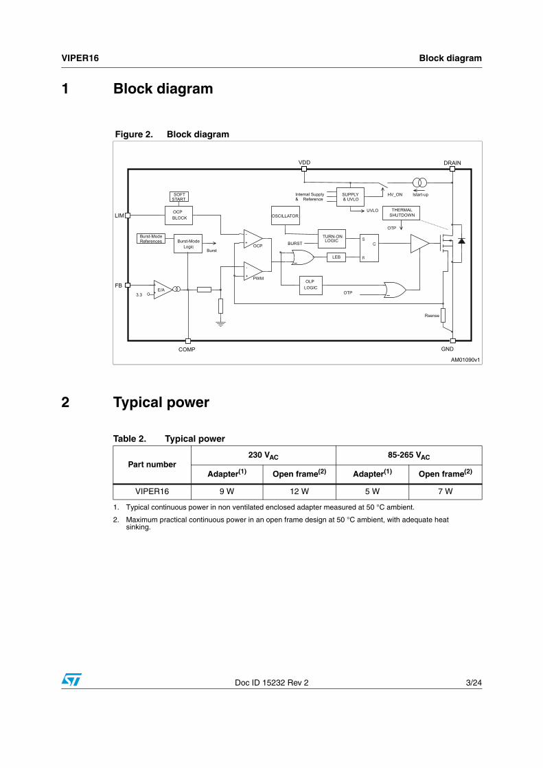
VIPER16 Block diagram
Doc ID 15232 Rev 2 3/24
1 Block diagram
2 Typical power
Figure 2. Block diagram
Table 2. Typical power
Part number230 VAC 85-265 VAC
Adapter(1)
1. Typical continuous power in non ventilated enclosed adapter measured at 50 °C ambient.
Open frame(2)
2. Maximum practical continuous power in an open frame design at 50 °C ambient, with adequate heat sinking.
Adapter(1) Open frame(2)
VIPER16 9 W 12 W 5 W 7 W

Pin settings VIPER16
4/24 Doc ID 15232 Rev 2
3 Pin settings
Figure 3. Connection diagram (top view)
Note: The copper area for heat dissipation has to be designed under the DRAIN pins.
Table 3. Pin description
Pin N.Name Function
DIP-7 SO16
1 1-4 GNDConnected to the source of the internal power MOSFET and controller ground reference.
2 5 VDDSupply voltage of the control section. This pin provides the charging current of the external capacitor.
3 6 LIMThis pin allows setting the drain current limitation. The limit can be reduced by connecting an external resistor between this pin and GND. Pin left open if default drain current limitation is used.
4 7 FB
Inverting input of the internal trans conductance error amplifier. Connecting the converter output to this pin through a single resistor results in an output voltage equal to the error amplifier reference voltage (3.3 V typ. see VFB_REF on Table 7). An external resistors divider is required for higher output voltages.
5 8 COMP
Output of the internal trans conductance error amplifier. The compensation network have to be placed between this pin and GND to achieve stability and good dynamic performance of the voltage control loop. The pin is used also to directly control the PWM with an optocoupler. The linear voltage range extends from VCOMPL to VCOMPH (Table 7).
7,8 13-16 DRAINHigh voltage drain pin. The built-in high voltage switched start-up bias current is drawn from this pin too.
Pins connected to the metal frame to facilitate heat dissipation.

VIPER16 Electrical data
Doc ID 15232 Rev 2 5/24
4 Electrical data
4.1 Maximum ratings
4.2 Thermal data
Table 4. Absolute maximum ratings
SymbolPin
(DIP-7)Parameter
ValueUnit
Min Max
VDRAIN 7, 8 Drain-to-source (ground) voltage 800 V
EAV 7, 8 Repetitive avalanche energy (limited by TJ = 150 °C) 2 mJ
IAR 7, 8 Repetitive avalanche current (limited by TJ = 150 °C) 1 A
IDRAIN 7, 8 Pulse drain current 2.5 A
VCOMP 5 Input pin voltage -0.3 3.5 V
VFB 4 Input pin voltage -0.3 4.8 V
VLIM 3 Input pin voltage -0.3 2.4 V
VDD 2 Supply voltage -0.3Self
limitedV
IDD 2 Input current 20 mA
PTOT
Power dissipation at TA < 40 °C (DIP-7) 1 W
Power dissipation at TA < 60 °C (SO16N) 1 W
TJ Operating junction temperature range -40 150 °C
TSTG Storage temperature -55 150 °C
Table 5. Thermal data
Symbol ParameterMax value
SO16N
Max value
DIP-7Unit
RthJPThermal resistance junction pin (Dissipated power = 1 W)
35 40 °C/W
RthJAThermal resistance junction ambient (Dissipated power = 1 W)
90 110 °C/W
RthJAThermal resistance junction ambient (1)
(Dissipated power = 1 W)
1. When mounted on a standard single side FR4 board with 100 mm2 (0.155 sq in) of Cu (35 μm thick)
80 90 °C/W
Electrical data VIPER16
6/24 Doc ID 15232 Rev 2
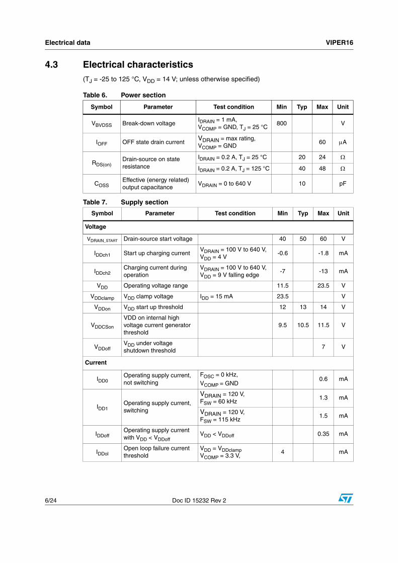
4.3 Electrical characteristics (TJ = -25 to 125 °C, VDD = 14 V; unless otherwise specified)
Table 6. Power section
Symbol Parameter Test condition Min Typ Max Unit
VBVDSS Break-down voltageIDRAIN = 1 mA, VCOMP = GND, TJ = 25 °C
800 V
IOFF OFF state drain currentVDRAIN = max rating, VCOMP = GND
60 μA
RDS(on)Drain-source on state resistance
IDRAIN = 0.2 A, TJ = 25 °C 20 24 Ω
IDRAIN = 0.2 A, TJ = 125 °C 40 48 Ω
COSSEffective (energy related) output capacitance
VDRAIN = 0 to 640 V 10 pF
Table 7. Supply section
Symbol Parameter Test condition Min Typ Max Unit
Voltage
VDRAIN_START Drain-source start voltage 40 50 60 V
IDDch1 Start up charging currentVDRAIN = 100 V to 640 V, VDD = 4 V
-0.6 -1.8 mA
IDDch2Charging current during operation
VDRAIN = 100 V to 640 V, VDD = 9 V falling edge
-7 -13 mA
VDD Operating voltage range 11.5 23.5 V
VDDclamp VDD clamp voltage IDD = 15 mA 23.5 V
VDDon VDD start up threshold 12 13 14 V
VDDCSon
VDD on internal high voltage current generator threshold
9.5 10.5 11.5 V
VDDoffVDD under voltage shutdown threshold
7 V
Current
IDD0Operating supply current, not switching
FOSC = 0 kHz,
VCOMP = GND0.6 mA
IDD1Operating supply current, switching
VDRAIN = 120 V, FSW = 60 kHz
1.3 mA
VDRAIN = 120 V,FSW = 115 kHz
1.5 mA
IDDoffOperating supply current with VDD < VDDoff
VDD < VDDoff 0.35 mA
IDDolOpen loop failure current threshold
VDD = VDDclampVCOMP = 3.3 V,
4 mA

VIPER16 Electrical data
Doc ID 15232 Rev 2 7/24
Table 7. Controller section(TJ = -25 to 125 °C, VDD = 14 V; unless otherwise specified)
Symbol Parameter Test condition Min Typ Max Unit
Error amplifier
VREF_FB FB reference voltage 3.2 3.3 3.4 V
IFB_PULL UP Current pull up -1 μA
GM Trans conductance 2 mA/V
Current setting (LIM) pin
VLIM_LOW Low level clamp voltage ILIM = -100 μA 0.5 V
Compensation (COMP) pin
VCOMPH Upper saturation limit TJ = 25 °C 3 V
VCOMPL Burst mode threshold TJ = 25 °C 1 1.1 1.2 V
VCOMPL_HYS Burst mode hysteresis TJ = 25 °C 40 mV
HCOMP ΔVCOMP / ΔIDRAIN 4 9 V/A
RCOMP(DYN) Dynamic resistance VFB = GND 15 kΩ
ICOMP
Source / sink current VFB > 100 mV 150 μA
Max source current VCOMP = GND, VFB = GND 220 μA
Current limitation
IDlim Drain current limitation
ILIM = -10 μA
VCOMP = 3.3 VTJ = 25 °C
0.38 0.4 0.42 A
tSS Soft-start time 8.5 ms
TON_MIN Minimum turn ON time 450 ns
IDlim_bmBurst mode current limitation
VCOMP = VCOMPL 85 mA
Overload
tOVL Overload time 50 ms
tRESTART Restart time after fault 1 s
Oscillator section
FOSCSwitching frequency VIPer16LN
54 60 66 kHz
Switching frequency
VIPer16HN103 115 127 kHz
FD Modulation depth FOSC = 60 kHz ±4 kHz
FOSC = 115 kHz ±8 kHz
FM Modulation frequency 230 Hz

Electrical data VIPER16
8/24 Doc ID 15232 Rev 2
Symbol Parameter Test condition Min Typ Max Unit
DMAX Maximum duty cycle 70 80 %
Thermal shutdown
TSDThermal shutdown temperature
150 160 °C
THYSTThermal shutdown hysteresis
30 °C
Table 7. Controller section (continued)(TJ = -25 to 125 °C, VDD = 14 V; unless otherwise specified)

VIPER16 Typical electrical characteristics
Doc ID 15232 Rev 2 9/24
5 Typical electrical characteristics
Figure 4. IDlim vs TJ Figure 5. FOSC vs TJ
Figure 6. VDRAIN_START vs TJ Figure 7. HCOMP vs TJ
Figure 8. GM vs TJ Figure 9. VREF_FB vs TJ

Typical electrical characteristics VIPER16
10/24 Doc ID 15232 Rev 2
Figure 10. ICOMP vs TJ Figure 11. Operating supply current(no switching) vs TJ
Figure 12. Operating supply current (switching) vs TJ
Figure 13. IDlim vs RLIM
Figure 14. Power MOSFET on-resistance vs TJ Figure 15. Power MOSFET break down voltage vs TJ

VIPER16 Typical circuit
Doc ID 15232 Rev 2 11/24
Figure 16. Thermal shutdown
6 Typical circuit
Figure 17. Buck converter

Typical circuit VIPER16
12/24 Doc ID 15232 Rev 2
Figure 18. Buck boost converter
Figure 19. Flyback converter (primary regulation)
VIPER16 Power section
Doc ID 15232 Rev 2 13/24
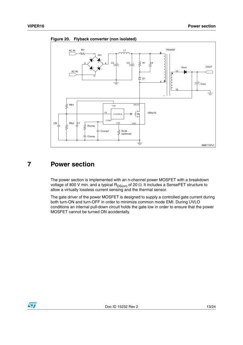
Figure 20. Flyback converter (non isolated)
7 Power section
The power section is implemented with an n-channel power MOSFET with a breakdown voltage of 800 V min. and a typical RDS(on) of 20 Ω. It includes a SenseFET structure to allow a virtually lossless current sensing and the thermal sensor.
The gate driver of the power MOSFET is designed to supply a controlled gate current during both turn-ON and turn-OFF in order to minimize common mode EMI. During UVLO conditions an internal pull-down circuit holds the gate low in order to ensure that the power MOSFET cannot be turned ON accidentally.

High voltage current generator VIPER16
14/24 Doc ID 15232 Rev 2
8 High voltage current generator
The high voltage current generator is supplied by the DRAIN pin. At the first start up of the converter, it is enabled when the voltage across the input bulk capacitor reaches the VDRAIN_START threshold (50 VDC typically), sourcing a 1 mA current (typical value); as the VDD voltage reaches the VDDon start-up threshold, the power section starts switching and the high voltage current generator is turned OFF. The VIPer16 is powered by the energy stored in the VDD capacitor.
In steady state condition, if the self biasing function is used, the high voltage current generator is activated between VDDCSon and VDDon (see Table 7), delivering 10 mA to the VDD capacitor during the MOSFET off time (see Figure 21).
The device can also be supplied through the auxiliary winding; in this case the high voltage current source is disabled during steady-state operation, provided that VDD is above VDDon.
At converter power-down, the VDD voltage drops and the converter activity stops as it falls below VDDoff threshold (see Table 7).
Figure 21. Flyback converter

VIPER16 Oscillator
Doc ID 15232 Rev 2 15/24
9 Oscillator
The switching frequency is internally fixed at 60 kHz (part number VIPER16LN) or 115 kHz (part number VIPER16HN).
In both cases the switching frequency is modulated by approximately ±4 kHz (60 kHz version) or ±8 kHz (115 kHz version) at 230 Hz (typical) rate, so that the resulting spread-spectrum action distributes the energy of each harmonic of the switching frequency over a number of sideband harmonics having the same energy on the whole but smaller amplitudes.
10 Soft start-up
During the converter start-up phase, the internal soft-start function progressively increases the cycle-by-cycle current limitation up to the IDlim value. In this way the drain current is further limited and the output voltage is progressively increased reducing the stress on the secondary diode. In combination with the control of the max duty cycle, this function helps to prevent transformer saturation during the start-up.
The soft-start time is internally fixed to 8.5 ms (see tSS on Table 7)and the function is activated for any attempt of converter start-up and after a fault event.
11 Adjustable current limit set point
The device is a current mode PWM: cycle-by-cycle the drain current is sensed and converted in a voltage that is applied to the non inverting pin of the PWM comparator and compared with the one present on the COMP pin (see Figure 2). When the two voltages values are equal, the power section is switched off.
Connecting a resistor RLIM between LIM and GND pins fixes the current sunk from the LIM pin and allows the designer to set the drain current limitation: it will be fixed to its default value, IDLIM on Table 7, if the LIM pin is left open or if the RLIM value is high enough (> 80 kΩ); it will be decreased, as reported in Figure 13 on page 10, if lower values of RLIM are chosen.

FB pin and COMP pin VIPER16
16/24 Doc ID 15232 Rev 2
12 FB pin and COMP pin
The device can be used both in non-isolated and in isolated topologies. In case of non-isolated topology, the feedback signal from the output voltage is applied to the FB pin and is compared with the error amplifier internal reference, VREF_FB (see Table 7). The error amplifier output sources and sinks the ICOMP current respectively to and from the compensation network connected on the COMP pin. The value of this voltage is then internally compared with the one coming from the SenseFET and the power section is switched off when the two values are equal on cycle by cycle basis.
As the regulation point on FB pin is 3.3 V, see VREF_FB on Table 7, a single resistor has to be connected to this pin if the output voltage is 3.3 V. While for higher output voltages an external resistor divider is needed. The FB pin is also provided with an internal pull up, in order to protect the IC when it is accidentally left floating.
The COMP pin, which is the output of the error amplifier, is used for the loop compensation: usually, an RC network, which stabilizes the overall control loop, is connected between this pin and GND.
In isolated topology, the FB pin is connected to GND, disabling the error amplifier. In this case a 15 kΩ internal resistor is connected between an internal 3.3 V generator and the COMP pin, which is also connected to an opto-transistor in parallel with the compensation network (see Figure 21).
The COMP pin voltage dynamics ranges is between VCOMPL and VCOMPH as reported in Figure 23 and Table 7.
At very low load or no load condition, when the voltage across the COMP pin drops below the voltage level VCOMPL - VCOMPL HYS, (where VCOMPL HYS is 50 mV typical), the converter enters burst mode (see Section 13 on page 17). When the COMP voltage rises above the VCOMPH threshold, the peak drain current will reach its limit, as well as the deliverable output power.
Figure 22. Feedback circuit Figure 23. COMP pin voltage versus IDLIM

VIPER16 Burst mode
Doc ID 15232 Rev 2 17/24
13 Burst mode
When the voltage at the COMP pin is 50 mV below an internally fixed threshold, VCOMPL, the power MOSFET is kept in OFF state and the consumption reduced at the lowest value. At this point, the voltage on the COMP pin increases as a result of the feedback reaction to the energy delivery stop. When the VCOMPL threshold is exceeded, the converter will start switching again. This controlled on-off operation, referred to as “burst mode”, causes an average frequency reduction, which can go down even to a few hundreds hertz, thus minimizing all frequency-related losses and making it easier to comply with energy saving regulations. This mode of operation, shown in the timing diagram of Figure 24, is noise-free since the peak current is very low.
Figure 24. Load-dependent operating modes: timing diagrams

Autorestart after fault VIPER16
18/24 Doc ID 15232 Rev 2
14 Autorestart after fault
In case of over load or short circuit, a counter increments every cycle the current-step logic detects a current limit condition; i.e. when the drain current reaches the IDLIM value (or the one set by the user through the Rlim resistor). If this condition is maintained continuously for a fixed-time, tOVL, the overload protection is tripped, the power section is turned off and the converter is disabled for a tRESTART time, whose typical value is 1 s (see Table 7). After the start-up sequence, the protection will occur in the same way until the overload condition is removed.
This protection ensures restart attempts of the converter with low repetition rate, so that it works safely with extremely low power throughput and avoiding the IC overheating in case of repeated overload events.
If the overload is removed before the protection tripping, the counter will be decremented cycle-by-cycle down to zero.
Figure 25. Timing diagram: OLP sequence

VIPER16 Open loop failure protection
Doc ID 15232 Rev 2 19/24
15 Open loop failure protection
When the VIPER16 is supplied by an auxiliary winding, the converter is protected against feedback loop failure or accidentally disconnections.
With reference to Figure 22, if resistance R1 is opened, the VIPER16 works at its drain current limitation.
The output voltage will increase and so the auxiliary voltage, which is coupled with the output through the secondary/auxiliary turns ratio.
As the auxiliary voltage increases up to the internal VDD active clamp, VDDclamp (see Table 7) and the clamp current injected on VDD pin exceeds the latch threshold, IDDol (see Table 7), a fault signal is internally generated.
Both the conditions: drain current equal to the drain current limitation and IDDol through VDD clamp, have to be verified to let the fault be revealed. This helps to distinguish an actual malfunction from a bad auxiliary winding design.
With reference to Figure 22, if the resistor R2 is opened, the FB pin is pulled up via R1, and the output voltage is clamped to VREF_FB (3.3 V, typ).
In case of accidental disconnection of the track on FB, the voltage on this pin goes up due to an internal pull-up, thus avoiding the power section switching.
In case of isolated flyback topology with auxiliary winding, the open loop failure protection will be triggered in the same way as described before, when the upper resistor of the output voltage divider, RUP, is opened or the lower resistor, RDOWN is shorted. If, on the contrary, RUP is shorted or RDOWN is opened, the output voltage will be limited to the voltage reference.

Package mechanical data VIPER16
20/24 Doc ID 15232 Rev 2
16 Package mechanical data
In order to meet environmental requirements, ST offers these devices in different grades of ECOPACK® packages, depending on their level of environmental compliance. ECOPACK® specifications, grade definitions and product status are available at: www.st.com. ECOPACK® is an ST trademark.
1- The leads size is comprehensive of the thickness of the leads finishing material.
2- Dimensions do not include mold protrusion, not to exceed 0,25 mm in total (both side).
3- Package outline exclusive of metal burrs dimensions.
4- Datum plane “H” coincident with the bottom of lead, where lead exits body.
5- Ref. POA MOTHER doc. 0037880
6- Creepage distance > 800 V
7- Creepage distance 250 V
8- Creepage distance as shown in the 664-1 CEI / IEC standard.
Table 8. DIP-7 mechanical data
Dim.mm
Typ Min Max
A 5,33
A1 0,38
A2 3,30 2,92 4,95
b 0,46 0,36 0,56
b2 1,52 1,14 1,78
c 0,25 0,20 0,36
D 9,27 9,02 10,16
E 7,87 7,62 8,26
E1 6,35 6,10 7,11
e 2,54
eA 7,62
eB 10,92
L 3,30 2,92 3,81
M (6)(8) 2,508
N 0,50 0,40 0,60
N1 0,60
O (7)(8) 0,548

VIPER16 Package mechanical data
Doc ID 15232 Rev 2 21/24
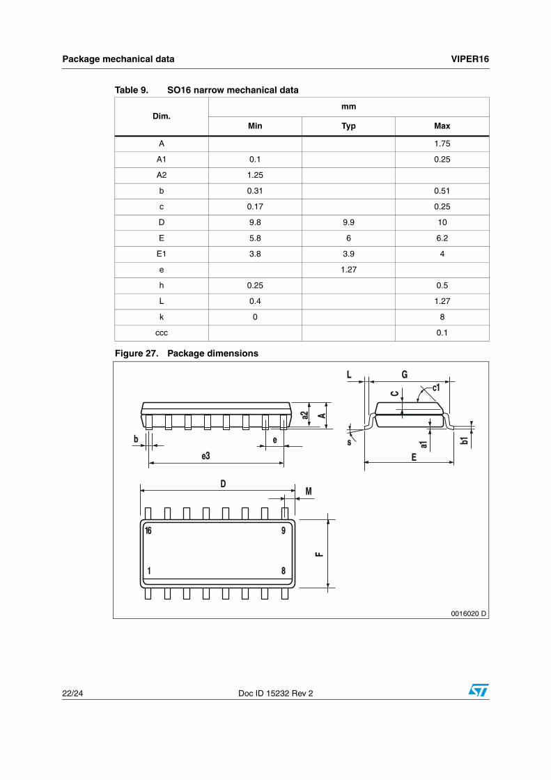
Figure 26. Package dimensions
Package mechanical data VIPER16
22/24 Doc ID 15232 Rev 2
Figure 27. Package dimensions
Table 9. SO16 narrow mechanical data
Dim.mm
Min Typ Max
A 1.75
A1 0.1 0.25
A2 1.25
b 0.31 0.51
c 0.17 0.25
D 9.8 9.9 10
E 5.8 6 6.2
E1 3.8 3.9 4
e 1.27
h 0.25 0.5
L 0.4 1.27
k 0 8
ccc 0.1
0016020 D

VIPER16 Revision history
Doc ID 15232 Rev 2 23/24
17 Revision history
Table 10. Document revision history
Date Revision Changes
21-Jan-2009 1 Initial release
07-Dec-2009 2 Updated Figure 7 on page 9

VIPER16
24/24 Doc ID 15232 Rev 2
Please Read Carefully:
Information in this document is provided solely in connection with ST products. STMicroelectronics NV and its subsidiaries (“ST”) reserve theright to make changes, corrections, modifications or improvements, to this document, and the products and services described herein at anytime, without notice.
All ST products are sold pursuant to ST’s terms and conditions of sale.
Purchasers are solely responsible for the choice, selection and use of the ST products and services described herein, and ST assumes noliability whatsoever relating to the choice, selection or use of the ST products and services described herein.
No license, express or implied, by estoppel or otherwise, to any intellectual property rights is granted under this document. If any part of thisdocument refers to any third party products or services it shall not be deemed a license grant by ST for the use of such third party productsor services, or any intellectual property contained therein or considered as a warranty covering the use in any manner whatsoever of suchthird party products or services or any intellectual property contained therein.
UNLESS OTHERWISE SET FORTH IN ST’S TERMS AND CONDITIONS OF SALE ST DISCLAIMS ANY EXPRESS OR IMPLIEDWARRANTY WITH RESPECT TO THE USE AND/OR SALE OF ST PRODUCTS INCLUDING WITHOUT LIMITATION IMPLIEDWARRANTIES OF MERCHANTABILITY, FITNESS FOR A PARTICULAR PURPOSE (AND THEIR EQUIVALENTS UNDER THE LAWSOF ANY JURISDICTION), OR INFRINGEMENT OF ANY PATENT, COPYRIGHT OR OTHER INTELLECTUAL PROPERTY RIGHT.
UNLESS EXPRESSLY APPROVED IN WRITING BY AN AUTHORIZED ST REPRESENTATIVE, ST PRODUCTS ARE NOTRECOMMENDED, AUTHORIZED OR WARRANTED FOR USE IN MILITARY, AIR CRAFT, SPACE, LIFE SAVING, OR LIFE SUSTAININGAPPLICATIONS, NOR IN PRODUCTS OR SYSTEMS WHERE FAILURE OR MALFUNCTION MAY RESULT IN PERSONAL INJURY,DEATH, OR SEVERE PROPERTY OR ENVIRONMENTAL DAMAGE. ST PRODUCTS WHICH ARE NOT SPECIFIED AS "AUTOMOTIVEGRADE" MAY ONLY BE USED IN AUTOMOTIVE APPLICATIONS AT USER’S OWN RISK.
Resale of ST products with provisions different from the statements and/or technical features set forth in this document shall immediately voidany warranty granted by ST for the ST product or service described herein and shall not create or extend in any manner whatsoever, anyliability of ST.
ST and the ST logo are trademarks or registered trademarks of ST in various countries.
Information in this document supersedes and replaces all information previously supplied.
The ST logo is a registered trademark of STMicroelectronics. All other names are the property of their respective owners.
© 2009 STMicroelectronics - All rights reserved
STMicroelectronics group of companies
Australia - Belgium - Brazil - Canada - China - Czech Republic - Finland - France - Germany - Hong Kong - India - Israel - Italy - Japan - Malaysia - Malta - Morocco - Philippines - Singapore - Spain - Sweden - Switzerland - United Kingdom - United States of America
www.st.com


![SPAWALNICTWO 10stan-mar.net/katalogi/rozne-spawalnicze.pdf · 2012. 8. 27. · VIPER 170D VIPER 170D VIPER 205D VIPER 225D PROFI Napięcie zasilania [V] 230/50Hz 230/50Hz 230/50Hz](https://img.dokumen.tips/doc/110x75/6125f2e6be651f2c7632063d/spawalnictwo-10stan-marnetkatalogirozne-2012-8-27-viper-170d-viper-170d.jpg)