Embed Size (px)
Citation preview

SURFACE AND INTERFACE ANALYSIS, VOL. 25, 374È379 (1997)
First Results from the Microscopy BeamlineESCAon ELETTRA
L. Casalis,1 L. Gregoratti,1 M. Kiskinova,1,* G. Margaritondo,1 F. M. Braz Fernandes,2 R. J. Silva,2G. R. Morrison3 and A. W. Potts31 Sincrotrone Trieste, Padriciano 99, Trieste 34012, Italy2 Materials Science Department, FCT, Universidade Nova de Lisboa, 2825 Monte de Caparica, Portugal3 Department of Physics, KingÏs College, University of London, Strand, London WC2R 2LS, UK
The results of the Ðrst experiments with test samples, tool steel and polycrystalline Sn carried out with the scanningphotoemission microscope built on the ELETTRA storage ring in Trieste are presented and discussed. The scan-ning photoemission microscope uses a zone plate optical system for demagniÐcation of the photon beam to sub-micron dimensions. The present performance of the microscope in photoemission allows elemental and chemicalmapping and small-spot photoelectron spectroscopy with lateral resolution better than 200 nm. The reported resultsshow how photoemission microscopy can distinguish the spatial distribution of carbide phases with di†erent Fecontent at the surface of a tool steel and the correlation between inhomogeneous oxidation of a polycrystalline Snsample and its grain structure. 1977 by John Wiley & Sons, Ltd.(
Surf. Interface Anal. 25, 374È379 (1997)No. of Figures : 6 No. of Tables : 0 No. of Refs. 19
INTRODUCTION
The advantage of photoemission spectromicroscopycompared to conventional photoemission spectroscopyis that it can provide spatially resolved informationabout the chemical composition of the sample surfaceby collecting photoelectrons with a speciÐc kineticenergy originating from a small spot.1h6 Many areas ofphysics, chemistry and materials research can beneÐtfrom the capabilities of spectromicroscopy. Theyinclude studies of micro- and nano-structured surfaces,friction-induced wearing of surfaces, imperfections inanti-corrosion Ðlms, inhomogeneities at multi-component metal semiconductor interfaces, impuritysegregation and reactivity variations at surfaces relatedto grain boundaries, plane orientations and defects on amicroscopic scale, etc. The importance and the broadrange of possible applications of spectromicroscopyhave been recognized and recently led to constructionof UV and x-ray photoemission microscopes at third-generation high-brightness synchrotron sources likeALS at Berkeley, ELETTRA in Trieste and SRRC inTaiwan.
This paper reports the Ðrst results obtained with thescanning photoemission microscope (SPEM) connectedto the U2-undulator beamline on ELETTRA. Theyinclude : measurements on a test specimen, whichcompare the lateral resolution in transmission andphotoemission and show the present routinely achievedresolution in photoemission ; studies of the inhomoge-neous distribution of carbide phases on the surface of a
* Correspondence to : M. Kiskinova.
tool steel sample ; and studies of inhomogeneous oxida-tion of a polycrystalline Sn sample.
EXPERIMENTAL
The coherent light for the SPEM was provided by anundulator and monochromatized by a spherical gratingmonochromator with Ðxed entrance and exit slits,designed to work in the 250È1000 eV photon energyrange.7 At present the beamline is optimized to work inthe 400È650 eV range. The measurement station con-sists of three ultrahigh vacuum (UHV) chambers. Theone connected to the beamline hosts the SPEM. It isUHV connected to the other two chambers, where low-energy electron di†raction (LEED), Auger electronspectroscopy (AES), scanning tunnelling microscopy(STM) and other basic techniques for sample cleaningand preparation can be used. The specimen can beintroduced through a fast-entry lock and transported todi†erent ports using magnetic arms and a wobble stick.The experiments described here were performed withphoton energies in the range 490È600 eV.
In the SPEM, the incident photon beam is demagni-Ðed to a submicron size using a zone plate opticalsystem.3,7 The x-ray microscope can operate both intransmission and photoemission, collecting informationfrom a small spot or providing two-dimensional mapsby scanning the sample with respect to the photon spot.The spot size and working distance depend on theparameters of the zone plate and on the photon energy.Using amplitude zone plates with 100 lm diameter andouter zone width 100 nm, a resolution in photoemissionof better than 200 nm was reported for the Ðrst SPEM
CCC 0142È2421/97/050374È06 $17.50 Received 24 October 1996( 1997 by John Wiley & Sons, Ltd. Accepted 22 January 1997

ESCA MICROSCOPY BEAMLINE ON ELETTRA 375
built in the USA.1,4 The same type of zone plates areused in our microscope. The main advantage of thechosen focusing element is that it can cover a widephoton energy range (200È1000 eV) and the spatialresolution does not depend on the kinetic energy of theemitted photoelectrons. Another advantage of the zoneplate microscope is that, compared to electrostaticmicroscopes,5,6 charging and corrugation of the samplehave a negligible e†ect on the spatial resolution.
The SPEM on ELETTRA uses as a photoelectrondetector a 100 mm hemispherical (HS) capacitor elec-tron analyser with large-angle acceptance lenses and amultichannel (16 channels) detector (MCD). Photo-emission data collection is synchronized with the scan-ning drive and is organized in two modes : peak [ back-ground or multichannel detection. The Ðrst modeprovides direct information on the intensity variationsof the photoelectron peak by summing the signal of all16 channels at the peak maximum and subtracting thebackground signal monitored by the 16 channels a fewelectron-volts from the peak. This mode requires alonger acquisition time. It is used when the signal islow, which is the case of core levels with low cross-sections, or when the measurements require high energyresolution. In the second mode, the 16 channels arespread over an energy window determined by the passenergy (D10% of the pass energy). Depending on theselected kinetic energy window, the multichannel detec-tion mode makes concentration and/or chemicalmapping possible if the chemical shifts of the elementcore levels are detectable. Topographical and chemicalcontrast can be distinguished from each other by com-paring the contrast between the images taken by chan-nels positioned at the photoelectron peak and awayfrom it. Processing of the images taken in the multi-channel detection mode allows manipulation of pixelinformation, summing of all channels, selection andsubtraction of individual channels, etc. Despite thelower signal, the main difficulty at present is that themultichannel detection mode requires that the yieldvariations from channel to channel are small or that thevariations in detector sensitivity can be monitored andcorrected for. The conventional energy distributioncurve (EDC) spectra are usually taken on microspotsselected from the images. The ultrahigh brightness ofthe third-generation x-ray sources allows the wholeanalytical power of ESCA to be used in spectroscopymode in order to obtain information about the chemicalcomposition and local electronic structure of a probedarea of \200 nm.
Another working mode of the microscope is in trans-mission. The transmitted x-rays can be detected using ahigh-sensitivity photodiode. The signal from the photo-diode is ampliÐed and read by a programmable multim-eter (HP 34401A). This mode is important for rapidlyÐnding the exact focal distance. It can also be used forimaging transmitting samples, where the di†erence ofthe absorption coefficients of the elements will result incontrast variations. By selecting an appropriate photonenergy before or after the absorption edge of an elementof interest, the images taken in transmission can alsoprovide chemical information.
More details for the construction and components ofthe beamline and of the measurement station can befound in Ref. 7.
RESULTS
Imaging and resolution in transmission andphotoemission : test samples
The resolution tests in transmission, using the intensityrise across the edge of a pinhole mounted on a solidsupport that is directly attached to the scanning stage,are described in Ref. 7. From the 20È80% rise in theintensity across the knife edge, a spatial resolution of150 nm was measured for a zone plate with a theoreticalresolution of 122 nm.
The test sample used for demonstration that the samesubmicron resolution can be achieved in transmissionand photoemission was a holey carbon sample with adeposited gold Ðlm of 150 nm thickness. This testsample contains holes of micron and submicron sizesand made it possible to compare the performance of themicroscope in transmission and photoemission. Thetwo-dimensional micrographs shown in Figs 1(a) and1(b) were obtained with a photon energy of 590 eV. Theimages in photoemission were obtained by tuning to theAu photoelectrons using a peak [ background4f7@2detection mode. The analyser was operated with a passenergy of 22 eV and a dwell time of 200 ms. An acquisi-tion time of D150 min was required for a 129] 129pixel image. The imaging rate in transmission wasdetermined only by the scanning speed of the stage so
Figure 1. (Left) 6.5 Ã6.5 lm2 images of a holey carbon samplewith 150 nm Au film. (Right) Linescan profiles across the images.(a) Transmission image; (b) photoemission image (129 Ã129pixels).
( 1997 by John Wiley & Sons, Ltd. SURFACE AND INTERFACE ANALYSIS, VOL. 25, 374È379 (1997)

376 L CASALIS ET AL .
that acquisition of a 128 ] 128 pixel map with piezo-scanners required D8 min.
In transmission, the holes through which the photonÑux passes undisturbed appear as bright areas in Fig.1(a). In photoemission the contrast is reversed : the holesappear dark and the Au-covered areas appear bright.Linescans across the images, displayed on the right sideof each image, show the same proÐle across the holesedges. This indicates that the resolution in photoemiss-ion and transmission is the same, as expected consider-ing the short mean-free path of the photoelectrons.
The present routinely achievable spatial resolution inphotoemission, using transferable sample holders, isillustrated in Fig. 2. The images are of a test sample,namely an e-beam-written Ge star pattern on Si, andare obtained by tuning to the Ge 3d core levels. Figure2 demonstrates very well-resolved Ge features of \200nm. To our knowledge this is the best performance of azone plate scanning microscope obtained in photoe-mission, as far as spatial resolution and signal are con-cerned. Further improvements in the construction of thetransferable sample holder assembly to ensure parallel-ism of better than 1¡ between the sample and the opticalelements are necessary in order to approach the excel-lency of the transmission microscopes.
Here, it is worth commenting brieÑy on theresolution limitations of the scanning photoemissionmicroscopes. Besides the technical problems, imposedby the fact that the instrument requires ultrahighvacuum, a sample transfer system and in-situ prep-aration facilities, the main limitations remain theworking distance between the sample and the opticalassembly and the efficiency of the zone plate(determined by the pattern placement accuracy andphoton energy). The working distance is about half thefocal length, because an order sorting aperture shouldbe placed between the zone plate and the sample.1,3,7The relationship between the focal length f, zone plateparameters (diameter D and outer zone width dr) andphoton energy E (eV) are described by
f (mm)\ DdrE/1.24 ] 10~7 (1)
The present experience has shown that the closely posi-tioned optical system obstructs the path of the photoe-mitted photoelectrons from the sample to the analyser,so that a reasonable working distance of D2 mm or
more should be kept. Thus, in photoemission theimprovement of the spatial resolution, which meanssmaller dr, should always be compensated by increasingthe diameter of the zone plate. At present the pro-duction of high-resolution zone plates with an outerzone width \100 nm and a large diameter is still atechnologically difficult task. Note that the bestresolution in transmission of 50 nm is obtained with azone plate with parameters : dr \ 35 nm and D\ 50lm, which determine a focal length of only 0.6 mm at500 eV.3
Microspectroscopy and two-dimensional micrographs ofcarbon containing phases in a tool steel sample
The Ðrst experiments with the microscope on a “realÏobject were performed on a technological item: a toolsteel where the microstructures induced by thecoexisting surface carbide phases were distinguishedfrom each other. This inhomogeneity is usually linkedto the mechanical properties of steel, such as hardness,wearing, etc.
The sample was a tool steel (H13-AISI : average com-position in wt.% (at.%) of carbon and alloying ele-ments : 0.35 (1.6) C, 5 (5.3) Cr, 1.5 (0.8) Mo and 1 (1.2)V) ; quenched from a temperature of 1320 K and tem-pered at 820 K. In the case of the steel sample underconsideration, the annealing (during steel fabrication)and tempering can result in the formation of variouscarbide precipitates with di†erent carbon, Fe and alloy-ing element content.8,10 In the commonly observedcarbide phases, such as MC, and whereM6C M23C6 ,M stands for the metals contained in the steel sample,the carbides of alloying elements are the dominatingones.8,9 The expected sizes of the di†erent carbidephases range from a few tens of nanometres to a fewtens of micrometres. In the sample under investigationmartensite laths, where Fe is the dominating element,can range from around 10 to a few tens of micrometres.Martensite has a higher non-equilibrium content of dis-solved carbon, inducing distortion of the Fe cubiclattice. Obviously, on a microscopic scale one canexpect chemical heterogeneity resulting from the largevariety of alloy metal-enriched carbide phases and thepresence of dissolved carbon in the iron-based matrix.
Figure 2. 12.5 Ã12.5 lm2 (a) and 2.5 Ã2.5 lm2 (b) images of a Ge star pattern on Si (256 Ã256 pixels).
( 1997 by John Wiley & Sons, Ltd. SURFACE AND INTERFACE ANALYSIS, VOL. 25, 374È379 (1997)
ESCA MICROSCOPY BEAMLINE ON ELETTRA 377
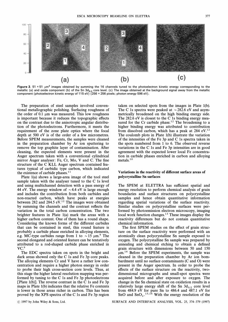
Figure 3. 51 Ã51 lm2 images obtained by summing the 16 channels tuned to the photoelectron kinetic energy corresponding to themetallic (a) and oxide component (b) of the Sn core level. (c) The image obtained at the background signal away from the metallic3d
5@2component (photoelectron kinetic energy of 115 eV) (256 Ã256 pixels ; photon energy 596 eV).
The preparation of steel samples involved conven-tional metallographic polishing. Surfacing roughness ofthe order of 0.1 lm was measured. This low roughnessis important because it reduces the topographic e†ectson the contrast due to the anisotropic angular distribu-tion of the photoelectrons. Furthermore, it meets therequirement of the zone plate optics where the focaldepth at 500 eV is of the order of a few micrometres.Before SPEM measurements, the samples were cleanedin the preparation chamber by Ar ion sputtering toremove the top graphite layer of contamination. Aftercleaning, the expected elements were present in theAuger spectrum taken with a conventional cylindricalmirror Auger analyser : Fe, Cr, Mo, V and C. The Ðnestructure of the C KLL Auger spectrum contained fea-tures typical of carbidic type carbon, which indicatedthe existence of carbide phases.11
Plate 1(a) shows a large-area image of the tool steelsample taken with the analyser tuned to the C 1s leveland using multichannel detection with a pass energy of44 eV. The energy window of D4.4 eV is large enoughand includes the contribution from both carbides andnon-reacted carbon, which have peaks at energiesbetween 282 and 284.5 eV.12 The images were obtainedby summing the channels and the contrast reÑects thevariation in the total carbon concentration. The twobrighter features in Plate 1(a) mark the areas with ahigher carbon content. One of them has a round shape.Considering the known forms of the di†erent carbidesthat can be contained in steel, this round feature isprobably a carbide phase enriched in alloying elements,e.g. MC-type carbides range from 1 to D15 lm.9 Thesecond elongated and oriented feature can be tentativelyattributed to a rod-shaped carbide phase enriched inVC.9
The EDC spectra taken on spots in the bright anddark areas showed only the C 1s and Fe 3p core peaks.The alloying elements Cr and V have a rather low con-centration and require a higher photon energy in orderto probe their high cross-section core levels. Thus, atthis stage the higher lateral resolution mapping was per-formed by tuning to the C 1s and Fe 3p photoelectrons[Plate 1(b)]. The reverse contrast in the C 1s and Fe 3pmaps in Plate 1(b) indicates that the relative Fe contentsis lower in those areas richer in carbon. This has beenproved by the XPS spectra of the C 1s and Fe 3p region
taken on selected spots from the images in Plate 1(b).The C 1s spectra were peaked at D282.6 eV and asym-metrically broadened on the high binding energy side.The 282.6 eV is closest to the C 1s binding energy mea-sured for the Cr carbide phase.12 The broadening to ahigher binding energy was attributed to contributionfrom dissolved carbon, which has a peak at 284 eV.12The coulomb plots in Plate 1(b) illustrate the variationof the intensities of the Fe 3p and C 1s spectra taken inthe spots numbered from 1 to 6. The observed reversevariations in the C 1s and Fe 3p intensities are in goodagreement with the expected lower local Fe concentra-tion in carbide phases enriched in carbon and alloyingmetals.10
Variations in the reactivity of di†erent surface areas ofpolycrystalline Sn surfaces
The SPEM at ELETTRA has sufficient spatial andenergy resolution to perform chemical analysis of grainboundaries and surface structures on polycrystallinesamples and hence obtain quantitative informationregarding spatial variations of the surface reactivity.Similar studies on polycrystalline surfaces were per-formed by photoemission electron microscopy, imaginglocal work function changes.13 These images display thereactivity di†erences but do not contain quantitativechemical information.
The Ðrst SPEM studies on the e†ect of grain struc-ture on the surface reactivity were performed with anatomically clean polycrystalline Sn sample exposed tooxygen. The polycrystalline Sn sample was prepared byannealing and chemical etching to obtain a deÐnedgrain structure with dimensions between 50 and 150lm.14 Before the SPEM experiments, the sample wascleaned in the preparation chamber by Ar ion bom-bardment until no surface contaminants (C and O) werepresent in the Auger spectrum. In order to probe thee†ects of the surface structure on the reactivity, two-dimensional micrographs and small-spot spectra wereacquired before and after exposure to oxygen. Thechange in the Sn chemical state on oxidation results in arelatively large energy shift of the Sn core level3d5@2from 484.9 eV for pure Sn to 486.4 and 487.1 eV forSnO and With the energy resolution of theSnO2 .15,16
( 1997 by John Wiley & Sons, Ltd. SURFACE AND INTERFACE ANALYSIS, VOL. 25, 374È379 (1997)

378 L CASALIS ET AL .
Figure 4. Small-spot EDC spectra of the Sn region taken3d5@2
from the areas (1) to (4) indicated in Fig. 3. Photon energy 596eV.
microscope of D0.5 eV, accurate chemical mappingwith photoelectron kinetic energy tuned to the metallicor oxide component of the Sn core level was pos-3d5@2sible.
Figure 3 shows images of the Sn sample after expo-sure to 1000 L of oxygen at 300 K. The images arecentred close to the corner of four grains. The chemicalmaps obtained with the analyser set for collectingphotoelectrons corresponding to the well-resolvedmetallic and oxide components of the Sn core3d5@2levels are displayed in panels (a) and (b), respectively.The contrast in the maps indicates a di†erence in theoxidation state of the di†erently oriented grains.
The di†erent stage of oxidation revealed by thechemical maps is conÐrmed by the Sn spectra dis-3d5@2played in Fig. 4. The spectra are taken from the spotson the four grains, numbered from 1 to 4 in Fig. 3. Thelarger width of the oxide-related peak has been associ-ated previously with the formation of both SnO and
in the oxidation process.17 From the small-spotSnO2spectra in Fig. 4 it is clear that the Sn/Sn oxide ratiovaries across the surface, in agreement with the contrastvariations observed in the images of Fig. 3.
Besides the four grains, another distinguishablefeature in the chemical maps in Fig. 3(a) and 3(b) are thedarker and brighter bands decorating the grain bound-aries. The image taken at the background signal anddisplayed in Fig. 3(c) indicates the topographic origin ofthese bands. It is notable that the very grazing take-o†angle of our analyser in order to gain surface sensitivityenhances the topographical artefacts. As submicronESCA imaging is a very recent achievement, methodsfor correction of topographic and subsurface inhomo-geneity e†ects are under development. The methodsused in scanning Auger microscopy,18 where the back-ground is simply determined by the inelastically scat-tered primary electrons, cannot be directly applied inphotoemission microscopy.
These Ðrst results show that it is possible to detectgrain e†ects on metal surfaces. This opens up theopportunity to study surface reactions with high spatialresolution. We would like to stress here that the greatadvantage of the SPEM is that it can distinguish thestructural impact on the surface reactivity by detailedexamination of the chemical composition and chemicalstate of the surface at a submicron level.
OUTLOOK
The results presented here show the capability of thescanning photoelectron microscope on ELETTRA as aresearch tool that can provide compositional andchemical information on a submicron scale. Combiningimaging tuned to di†erent core levels with small-spot
Figure 5. (Left) 6.5 Ã6.5 lm2 image of an Au ½Af/Si(111) interface tuned to the metallic component of the Ag core level. The bright3d5@3
features correspond to the three-dimensional subphase. (Right) Small-spot EDC spectra of the Ag 3d, Si 2p and Au 4f regions taken ontothe two- and three-dimensional areas. Photon energy 495 eV.
( 1997 by John Wiley & Sons, Ltd. SURFACE AND INTERFACE ANALYSIS, VOL. 25, 374È379 (1997)

ESCA MICROSCOPY BEAMLINE ON ELETTRA 379
spectroscopy made it possible to map the heterogeneousdistribution of carbide phases of a steel sample and toidentify spatial variations in the oxidation state of apolycrystalline Sn sample controlled by the presence ofgrain boundaries.
The most recent energy resolution improvements ofthe instrument allowed us to probe laterally heter-ogeneous metal/semiconductor interfaces and reveal thecomposition and chemical di†erences betweensubmicrometre-sized phases. Figure 5 illustrates space-resolved composition mapping and photoelectronspectromicroscopy results obtained for a multiphasebimetal/silicon interface. The images and spectra in Fig.6 are taken at the metallic Ag level of the3d5@2Au ] Ag/Si(111) interface containing three-dimensionalmicroparticles of sizes O1 lm. The space-resolved Ag3d, Au 4f and Si 2p core-level spectra from the two-dimensional and three-dimensional phases haverevealed the di†erences in the local Au and Ag chemical
states in each phase : the three-dimensional particlescontain metallic Ag and Au, whereas the two-dimensional Ag] Au/Si phase contains only reactedAg and Au.17 This recent result pinpoints an importantand almost unexplored application Ðeld for the micro-scope : chemical processes localized on sub-micronphases of morphologically complex interfaces.
Acknowledgements
We gratefully acknowledge P. Melpignano for her valuable contribu-tion to alignment and testing of the zone plate system, R. Krempaskaand R. Pugliese for upgrading the data acquisition programs andSandrin and D. Lonza for their excellent technical assistance. Themost recent results were obtained in collaboration with S. Guenther,A. Kolmakov and J. Kovac. The research was supported by an ECgrant under contract ERBCHGECT920013 and by SincrotroneTrieste SCpA.
REFERENCES
1. H. Ade, J. Kirz, S. Hulbert, E. Johnson, E. Anderson and D.Kern,Nucl . Instrum.Methods A291, 126 (1990).
2. G. Margaritondo and F. Cerrina, Nucl . Instrum. MethodsA291, 26 (1990) and references therein.
3. J. J. Kirz, Ch. Jacobsen and M. Howells, Q. Rev. Biol . 28, 33(1995) and references therein.
4. C.-H. Ko, J. Kirz, K. Maier, B. Winn, H. Ade, S. Hulbert, E.Johnson and E. Anderson, Proc. SPIE on X-ray MicrobeamTechnology and Applications , p. 2516 (1995).
5. B. P. Tonner and G. R. Harp, Rev. Sci . Instrum. 59, 853(1988).
6. E. Bauer, Ultramicroscopy 36, 52 (1991) and referencestherein.
7. L. Casalis, W. Jark, M. Kiskinova, D. Lonza, P. Melpignano, D.Morris, R. Rosei, A. Savoia, et al ., Rev. Sci . Instrum. 66, 4870(1995).
8. H. J. Goldschmidt, JISI , p. 345 (1948).9. J. Richter, M. Hetmanczuk and J. Cwajna, J. Mater . Process
Techol . 53, 34 (1995).10. R. C. Thomson and M. K. Miller, Appl . Surf . Sci . 87/88, 185
(1995).
11. E. L. Davis, N. C. MacDonald, W. P. Palmberg, G. E. Riachand E. R. Weber, Handbook of Auger Electron Spectroscopy.Physical Electronics Industries, Eden Prairie, MN (1976).
12. J. F. Moulder, W. F. Stickle, P. E. Sobol and K. D. Bomben,Handbook of X-ray Photoelectron Spectroscopy. Perkin-Elmer, Physical Electronics Division, Eden Prairie, MN (1992).
13. H. H. Rotermund, S. Jakubith, S. Kubala, A. von Oertzen andG. Ertl, J . Electron Spectrosc .Relat . Phenom. 52, 811 (1990).
14. A. W. Potts, S. Anjium, R. E. Burge, T. A. Tournas and A.Yacoot, Electron Spectrosc .Relat . Phenom. 61, 27 (1992).
15. J.-M. Themlin, M. Chtaib, L. Henrard, P. Lambin, J. Darvilleand J.-M. Gilles, Phys.Rev. B46, 2460 (1992).
16. G. Morelli, Z. Lovacs, R. Sanjines, I. Cserny, G. Margaritondo,J. Palinkas and H. Adachi, J . Vac. Sci . Technol . A13, 1383(1995).
17. R. Sanjines, C. Coluzaa, D. Rosenfeld, F. Gozzo, P. Almeras, F.Levi and G. Margaritondo, J.Appl . Phys. 73, 3997 (1993).
18. M. Prutton, I. R. Barkshire, M. Crone, Ultramicroscopy 59, 47(1995).
19. S. Gu� nther, J. Kovac, A. Kolmakov, M. Marsi and M. Kiskin-ova submittedPhys.Rev.B.
( 1997 by John Wiley & Sons, Ltd. SURFACE AND INTERFACE ANALYSIS, VOL. 25, 374È379 (1997)