Embed Size (px)
Citation preview
AT & S Austria Technologie & Systemtechnik Aktiengesellschaft | Fabriksgasse 13 | A-8700 Leoben Tel +43 (0) 3842 200-0 | E-Mail [email protected]
www.ats.net
AT&S First choice for advanced applications
Investor and Analyst Presentation
May 2017

Company Overview
Strategy & Market
Annex
Financials
Table of Contents
1

High-end interconnect
solutions for
Mobile Devices, Automotive,
Industrial, Medical Applications
and Semiconductor Industry
Continuously
outperforming
market growth
€ 814.9m revenue in FY 2016/17
# 1 manufacturer in Europe
# 3 in high-end technology
worldwide
9,526 employees
Cost-competitive production
footprint with
6 plants in Europe and Asia
AT&S – a world leading high-tech PCB and IC substrates company
2
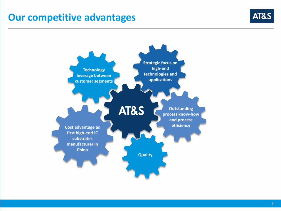
Outstanding process know-how
and process efficiency
Our competitive advantages
Cost advantage as first high-end IC
substrates manufacturer in
China
Strategic focus on high-end
technologies and applications
Technology leverage between
customer segments
Quality
3
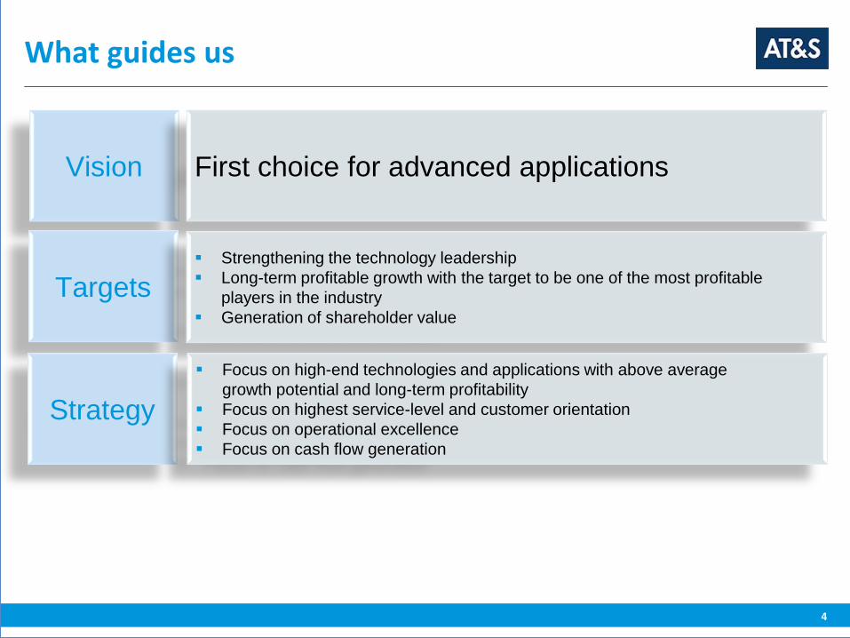
What guides us
Vision First choice for advanced applications
Targets
Strengthening the technology leadership
Long-term profitable growth with the target to be one of the most profitable
players in the industry
Generation of shareholder value
Strategy
Focus on high-end technologies and applications with above average
growth potential and long-term profitability
Focus on highest service-level and customer orientation
Focus on operational excellence
Focus on cash flow generation
4
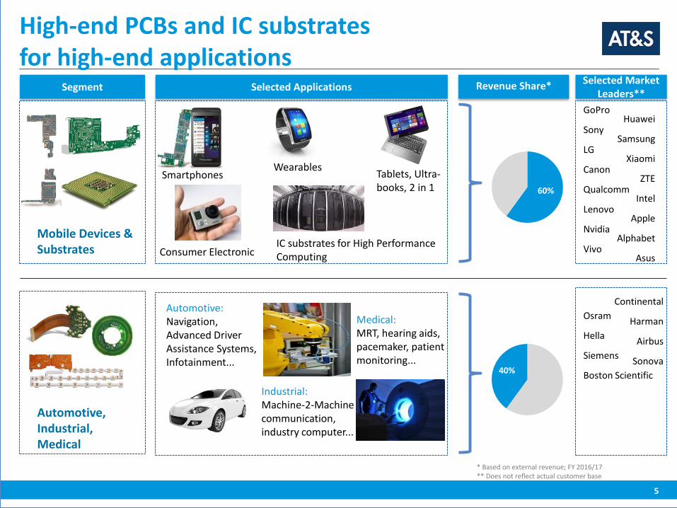
High-end PCBs and IC substrates for high-end applications
Revenue Share*
Segment Selected Market
Leaders**
GoPro
Sony
LG
Canon
Qualcomm
Lenovo
Nvidia
Vivo
Huawei
Samsung
Xiaomi
ZTE
Intel
Apple
Alphabet
Asus
Selected Applications
Osram
Hella
Siemens
Boston Scientific
Continental
Harman
Airbus
Sonova
Mobile Devices & Substrates
Automotive, Industrial, Medical
Consumer Electronic
Smartphones Wearables
Tablets, Ultra-books, 2 in 1
Automotive: Navigation, Advanced Driver Assistance Systems, Infotainment...
Industrial: Machine-2-Machine communication, industry computer...
Medical: MRT, hearing aids, pacemaker, patient monitoring...
* Based on external revenue; FY 2016/17 ** Does not reflect actual customer base
60%
40%
5
IC substrates for High Performance Computing
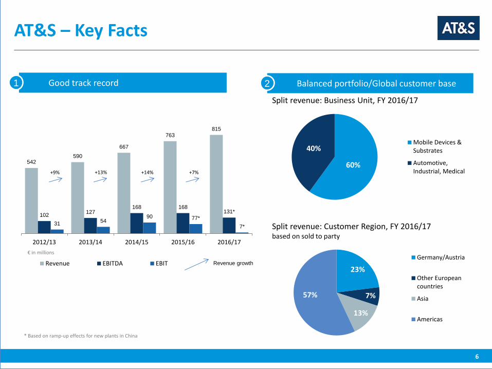
542 590
667
763 815
102 127
168 168 131*
31 54
90 77*
7*
2012/13 2013/14 2014/15 2015/16 2016/17
Revenue EBITDA EBIT
AT&S – Key Facts
Good track record 1 Balanced portfolio/Global customer base 2
7%
Split revenue: Business Unit, FY 2016/17
Split revenue: Customer Region, FY 2016/17 based on sold to party
+9% +13% +14% +7%
* Based on ramp-up effects for new plants in China
Revenue growth
€ in millions
6
60%
40% Mobile Devices &Substrates
Automotive,Industrial, Medical
23%
7%
13%
57%
Germany/Austria
Other Europeancountries
Asia
Americas

Global footprint ensures proximity to supply chain & cost efficiency
European production facilities: high mix/low volume Asian production facilities: high volume/low mix
Sales network spanning three continents 9,526 employees*
Plant Shanghai, China Staff: 4,583*
Plant Ansan, Korea Staff: 300*
Plant Nanjangud, India Staff: 1,134*
Plant Chongqing, China In ramp phase Staff: 2,083*
Plant Leoben, Austria Headquarters Staff: 977*
Plant Fehring, Austria Staff: 372*
AT&S sales offices AT&S plants
* Average, FTE, FY 2016/17; 77 employees in other locations
7

14.6 14.5
15.3 17.3
7.6 8.7
5.2
6.1 3.7
4.5 2.4
2.8 48.8
53.9
2017 2021
Computing Communication
Consumer Automotive
Industrial/Medical Military/Aerospace
5.0%
4.0%
3.5%
(0.2%)
3.0%
PCB market – Overview
Source: Prismark, Feb. 2017; Yole Apr. 2017
Moderate growth of 2.4% forecast for the total PCB market until 2021.
CAAGR 2017-2021: 2.4%
3.8%
USD in billions
8
AT&S outperformed a flat market in the past 6 years and is set to continue to do so also in the future.
100.5 101.3 103.7 96.9 95.1
105.4 114.8
129.8
148.4 158.5
2011* 2012 2013 2014 2015 2016
Index (2011 = 100)*
PCB & substrates market AT&S revenue
* Basis 2011: PCB & substrates market: USD 55.4bn AT&S revenue: € 514m
AT&S outperformed the market by scaling high-end any-layer technology and by leveraging HDI technology to the Computer-, Consumer-, Automotive-, Industrial and Medical market.
Company Overview
Strategy & Market
Annex
Financials
Table of Contents
9

10
AT&S positioning – Current
Strategic focus on high-end technologies
AT&S revenue structure in 2015/16 – based on technologies
High-end HDI PCBs and IC substrates
~ 30%
Single-sided (SS), double-sided (DS), multilayer (ML), flex and rigid-flex (RF) PCBs
~ 70%
High-end technology share > 70% HDI and any-layer PCBs, Embedding
Complementary technology share: < 30% SS, DS, ML,
Flex, RF
Structure of general PCB market – based on technologies

11
Source: Prismark 2016; NTI 2016; AT&S Strategy
* N/A due to single customer
Market position HDI Technology
Revenue (USD in millions)
Rank Country Supplier HDI Non HDI
PCBs IC
substrates Total
revenue
1 TWN Unimicron 802 490 830 2,122
2 TWN Compeq 679 716 - 1,395
3 AUT AT&S 596 248 -* 844
4 USA TTM 501 1,987 - 2,488
5 JPN Ibiden 368 - 929 1,297
6 TWN Tripod 316 1,052 - 1,368
7 TWN Unitech 311 123 - 434
8 KOR SEMCO 296 204 844 1,344
9 JPN Meiko 251 474 - 725
10 KOR DAP 226 - - 226
Market Player/Position HDI Technology
12
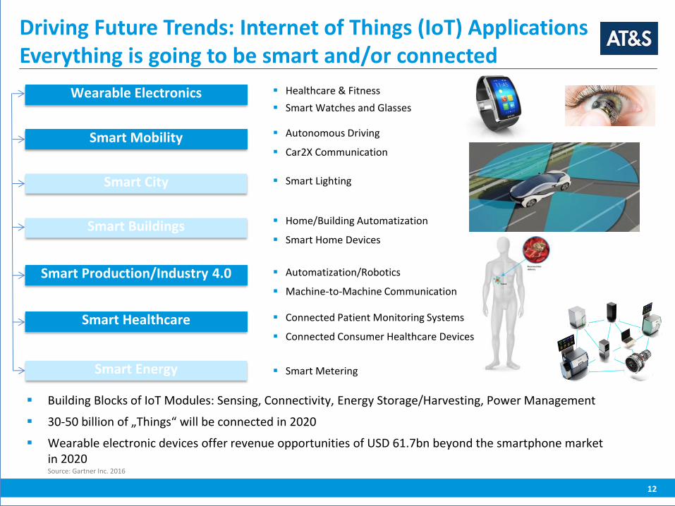
Driving Future Trends: Internet of Things (IoT) Applications Everything is going to be smart and/or connected
Healthcare & Fitness
Smart Watches and Glasses Wearable Electronics
Smart Mobility Autonomous Driving
Car2X Communication
Smart City Smart Lighting
Smart Buildings Home/Building Automatization
Smart Home Devices
Smart Production/Industry 4.0 Automatization/Robotics
Machine-to-Machine Communication
Smart Healthcare Connected Patient Monitoring Systems
Connected Consumer Healthcare Devices
Smart Energy Smart Metering
Building Blocks of IoT Modules: Sensing, Connectivity, Energy Storage/Harvesting, Power Management
30-50 billion of „Things“ will be connected in 2020
Wearable electronic devices offer revenue opportunities of USD 61.7bn beyond the smartphone market in 2020 Source: Gartner Inc. 2016
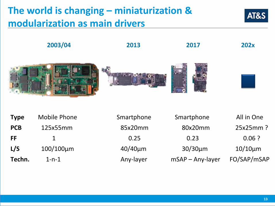
The world is changing – miniaturization & modularization as main drivers
2003/04 2013 2017 202x
?
Type Mobile Phone Smartphone Smartphone All in One
PCB 125x55mm 85x20mm 80x20mm 25x25mm ?
FF 1 0.25 0.23 0.06 ?
L/S 100/100µm 40/40µm 30/30µm 10/10µm
Techn. 1-n-1 Any-layer mSAP – Any-layer FO/SAP/mSAP
13

From vision to strategy
14
Targets/Key Performance Indicators
Strategy
Strengthening technology leadership • Leading player in the high-end core
business • Medium-term: leading player in new
business areas • Innovation Revenue Rate: > 20%
Continuous innovation and focus on high-end technologies and applications
Focus on innovative solutions
Long term profitable growth/to be one of the most profitable players in the industry • Medium-term EBITDA margin target of
18-20% • Medium-term revenue target of ~ € 1bn
Focus on technologies and applications with above- average growth potential and long-term profitability
Focus on highest service-level and customer orientation
Focus on operational excellence
Focus on cash flow generation
Generation of shareholder value • Medium term ROCE of 12%
Sustainable development focusing on ROCE
Stable dividend policy
Vision: “First choice for advanced
applications”
The best employees and executives • Talent Programs • Trainings • Leadership Excellence Program
Sustainable management To be the benchmark of the industry by reduction of: • 5% CO2 emissions p.a. • 3% freshwater consumption p.a.
Capital Excellence • Equity ratio: > 40% • Financing costs of < 2% (in a
corresponding interest environment) • Payback period of < 3 years

21.8% of AT&S‘ total revenue in 2016/17 is generated by products with new, innovative
technologies introduced to the market within the last three years (Innovation Revenue Rate).
196 patent families, resulting in 227 patents.
R&D expenses: € 62.8m in the financial year 2016/17.
R&D quota (i.e. relation to revenue): 7.7% (vs. 12.5% in the previous year).
24.7 31.8
57.9
95.5
62.8
2012/13 2013/14 2014/15 2015/16 2016/17
19.2
26.5 29.2
19.6 21.8
2012/13 2013/14 2014/15 2015/16 2016/17
124
153
174
212 227
2012/13 2013/14 2014/15 2015/16 2016/17
IRR (Innovation Revenue Rate)
€ in millions in % Quantity
Patents R&D expenses
Research and development as the key for technological leadership
15

Overview of the transformation from a high-end PCB manufacturer to a high-end interconnect solutions provider:
Core Business New technologies and interconnect
solutions
Extended Technology Toolbox
Additional customers
Additional applications
More comprehensive positioning in the value chain
Mo
re t
han
AT&
S
+
Future positioning as leading high-end interconnect solutions provider
16

17
AT&S’ advanced technology solutions
General Description & Technology Application Areas Customer Base
High-end (HDI) PCBs
PCBs are the interconnection platform for electric, electronic & mechanical components (such as resistors, capacitors, ICs,
connectors, etc.) Density: Line/Space > 35 micron
Computer, Consumer, Communication, Automotive
Industrial, Medical
OEMs Tier 1 Tier 2
Substrate-like PCBs
Substrate-like PCBs are the next evolution of high-end HDI PCBs with higher density: Line/Space < 30 micron
Mobile Applications like Wearables
OEMs Tier 1 Tier 2

18
General Description & Technology Application Areas Customer Base
IC substrates
IC substrates serve as interconnection platform with higher density (Line/Space < 15 micron) between
semiconductors (Chips) & PCBs
High-end processors for Computer, Communication,
Automotive, Industrial
OEMs Semiconductor
Industry
Embedded Component Packaging
(ECP®)
Embedded Component Packaging allows to embed active/passive components (e.g. wafer level dies) within the
layers of a PCB – contributes to miniaturization
Power Electronics, e.g. for
Automotive, Industrial
OEMs
Semiconductor Industry
AT&S’ advanced technology solutions

Growth Project Chongqing
IC substrate project Investment* Phase 1: ~ € 280m Investment* as of 31/03/2017: € 263m
mSAP project Investment* Phase 1**: ~ € 230m Investment* as of 31/03/2017: € 192m
IC substrates: > First production fully running; continuous improvement activities ongoing; high price pressure > Yield improvements follow internal development roadmap > 11 products for client computer and server qualified, 8 under qualification > Second production line started in December 2016; good performance > Target levels of both IC substrate lines to be achieved in the second half of calendar year 2017
Substrate-like PCBs -> mSAP > mSAP transformation ongoing: first production line currently updated to mSAP > Second production line under installation
CAPEX phase 2 of Chongqing: decision scheduled for summer 2017
* CAPEX for tangible fixed assets ** incl. investment of ~ € 30m for mSAP technology
19

20
Company Overview
Strategy & Market
Annex
Financials
Table of Contents
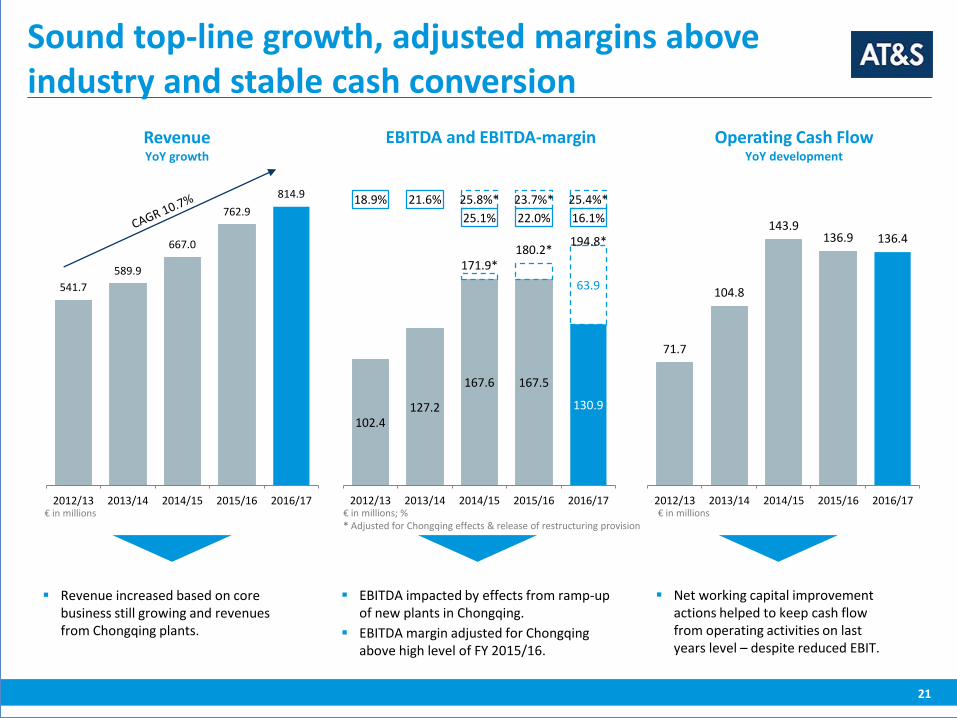
Sound top-line growth, adjusted margins above industry and stable cash conversion
Revenue YoY growth
Operating Cash Flow YoY development
EBITDA and EBITDA-margin
Revenue increased based on core business still growing and revenues from Chongqing plants.
EBITDA impacted by effects from ramp-up of new plants in Chongqing.
EBITDA margin adjusted for Chongqing above high level of FY 2015/16.
Net working capital improvement actions helped to keep cash flow from operating activities on last years level – despite reduced EBIT.
€ in millions
541.7
589.9
667.0
762.9
814.9
2012/13 2013/14 2014/15 2015/16 2016/17€ in millions € in millions; %
* Adjusted for Chongqing effects & release of restructuring provision
21
102.4 127.2
167.6 167.5
130.9
171.9*
63.9
180.2* 194.8*
25.1% 22.0% 16.1%
18.9% 21.6% 25.8%* 23.7%* 25.4%*
2012/13 2013/14 2014/15 2015/16 2016/17
71.7
104.8
143.9 136.9 136.4
2012/13 2013/14 2014/15 2015/16 2016/17

Flat revenue in core business due to stronger seasonality in Q1 and limited capacities in Q4 based on upgrade in Shanghai; revenue increase on segment level mainly based on Chongqing revenue
On EBITDA level: negative impacts from: Chongqing effects as well as price pressure both in core business and IC substrates, lost capacities in profitable core business; positive impacts: FX and cost savings
Adjusted EBITDA margin on last years high level
Business Development – Mobile Devices & Substrates
€ in millions (unless otherwise indicated)
2015/16 2016/17 Change in %
Revenue 539.7 573.0 6.2%
Revenue with external customers
452.5 486.5 7.5%
EBITDA 126.4 68.5 (45.8%)
EBITDA margin 23.4% 12.0% -
EBITDA adjusted* 139.6 135.7 (2.8%)
EBITDA margin adjusted* 26.0% 25.9% -
€ in millions; ** Revenue with external customers
Revenue per quarter**
22
* Adjusted for Chongqing effects
68.0
88.7
120.9 104.5 115.9 112.2
123.4
101.0 97.7
126.6
148.6
113.7
Q12014/15
Q22014/15
Q32014/15
Q42014/15
Q12015/16
Q22015/16
Q32015/16
Q42015/16
Q12016/17
Q22016/17
Q32016/17
Q42016/17
Trendline expressing seasonality
72.6 71.7
65.9
72.6
77.8 79.5 72.7 76.6
80.4 79.9 78.9
84.9
Q12014/15
Q22014/15
Q32014/15
Q42014/15
Q12015/16
Q22015/16
Q32015/16
Q42015/16
Q12016/17
Q22016/17
Q32016/17
Q42016/17
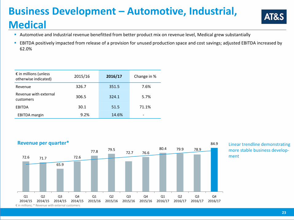
Automotive and Industrial revenue benefitted from better product mix on revenue level, Medical grew substantially
EBITDA positively impacted from release of a provision for unused production space and cost savings; adjusted EBITDA increased by 62.0%
Business Development – Automotive, Industrial, Medical
23
€ in millions; * Revenue with external customers
€ in millions (unless otherwise indicated)
2015/16 2016/17 Change in %
Revenue 326.7 351.5 7.6%
Revenue with external customers
306.5 324.1 5.7%
EBITDA 30.1 51.5 71.1%
EBITDA margin 9.2% 14.6% -
Revenue per quarter* Linear trendline demonstrating more stable business develop- ment

Net CAPEX & Staff
Net CAPEX Net CAPEX of € 240.7m in FY 2016/17 includes investments in Chongqing project (whereof € 169.2m) and technology investments in existing locations.
STAFF* Headcount increase primarily caused by project Chongqing.
€ in millions
40.5
90.3
164.8
254.3 240.7
2012/13 2013/14 2014/15 2015/16 2016/17
7,267 6,904 7,029 7,379 7,443
54 123
609 1,380
2,083 7,321 7,027
7,638
8,759 9,526
2012/13 2013/14 2014/15 2015/16 2016/17
Core business Employees Chongqing
* FTE; incl. contractors; average for the period
24

Financials FY 2016/17
€ in thousands (unless otherwise
stated)2015/16 2016/17
Change
YoYSTATEMENT OF PROFIT OR LOSS
Revenue 762,879 814,906 6.8%
produced in Asia 81.0% 82.0% 1.0pp
produced in Europe 19.0% 18.0% (1.0pp)
EBITDA 167,488 130,933 (21.8%)
EBITDA margin 22.0% 16.1% (5.9pp)
EBITDA adjusted 180,215 194,752 8.1%
EBITDA margin adjusted 23.7% 25.4% 1.7pp
EBIT 76,969 6,649 (91.4%)
EBIT margin 10.1% 0.8% (9.3pp)
EBIT adjusted 103,200 119,006 15.3%
EBIT margin adjusted 13.6% 15.5% 1.9pp
Finance costs – net (8,135) (17,499) (>100%)
Income taxes (12,883) (12,047) 6.5%
Profit/(loss) for the period 55,951 (22,897) (>100%)
Cash earnings 146,471 101,764 (30.5%)
Earnings per share € 1.44 (€ 0.59) (>100%)
Adjusted EBIT increased to € 119.0m benefitting from cost reductions and FX gains
25
Revenue increase of 6.8% mainly from additional capacities in Chongqing
Adjusted for Chongqing effects of € 71.2m and release of provision of € 7.3m EBITDA margin increase from prior year to 25.4%
Finance costs net increased due to FX € 7.3m and € 4.4m less capitalized interests

Financials FY 2016/17
€ in thousands (unless otherwise
stated)31 Mar 2016 31 Mar 2017 Change
STATEMENT OF FINANCIAL
POSITION
Non-current assets 866,338 1,029,363 18.8%
Current assets 478,312 407,331 (14.8%)
Equity 568,936 540,094 (5.1%)
Non-current liabilities 421,407 569,849 35.2%
Current liabilities 354,307 326,751 (7.8%)
Total assets 1,344,650 1,436,694 6.8%
Net debt 263,192 380,549 44.6%
Net debt/EBITDA 1.6x 2.9x 1.3pp
Net gearing 46.3% 70.5% 24.2pp
Net working capital 88,427 24,374 (72.4%)
Net working capital per revenue 11.6% 3.0% (8.6pp)
Equity ratio 42.3% 37.6% (4.7pp)
26
Reduction of € 28.0m due to € 22.9m net loss and € 14.0m dividend payment
Reflects high CAPEX for and financing start-up phase in Chongqing; Net debt/EBITDA of 2.9x
Includes results of net working capital optimization activities
Reduced to 37.6%; covenant at 35%

299
372 405
523
593
82
261 274
260 212
217
111 131
263
381
2012/13 2013/14 2014/15 2015/16 2016/17
Gross debt Financial assets and cash Net debt
2.1
0.9 0.8
1.6
2.9
2012/13 2013/14 2014/15 2015/16 2016/17
Expected multiple in temporary peak of Chongqing investments: ~ 3.5x
Net debt/EBITDA
Gross debt, financial assets and cash, net debt
Reflects high CAPEX for and financing start-up phase in Chongqing.
€ in millions
27
Gross debt, financial assets and cash, net debt
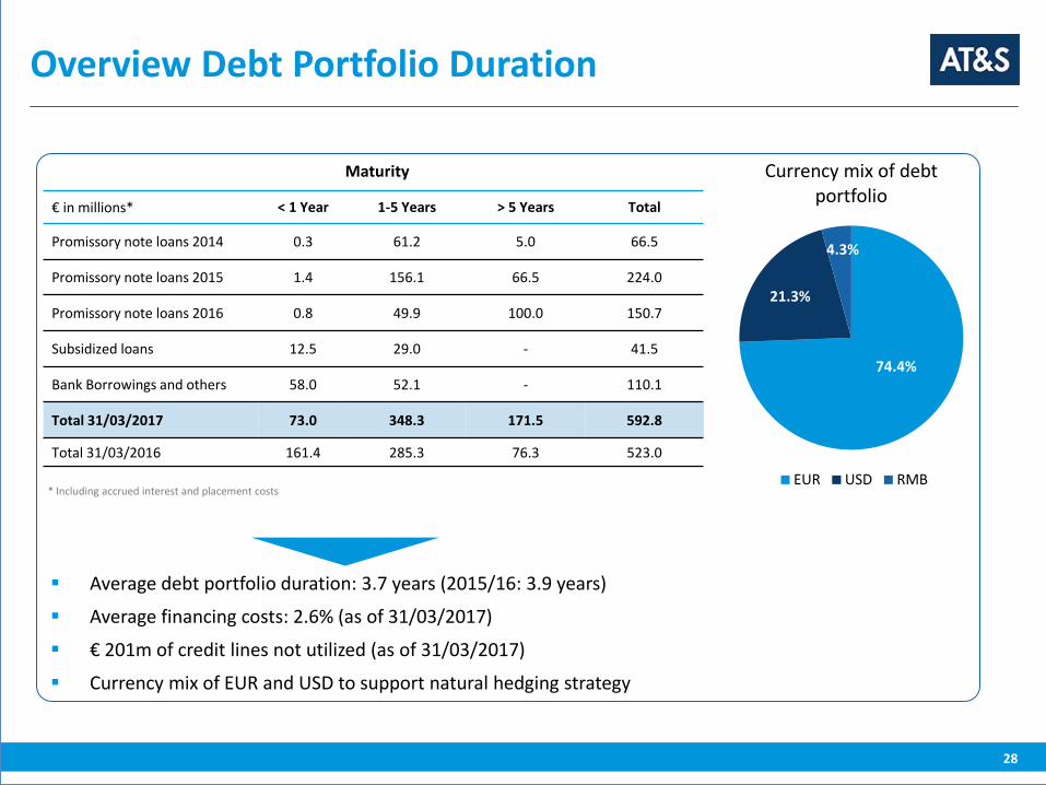
Overview Debt Portfolio Duration
Average debt portfolio duration: 3.7 years (2015/16: 3.9 years)
Average financing costs: 2.6% (as of 31/03/2017)
€ 201m of credit lines not utilized (as of 31/03/2017)
Currency mix of EUR and USD to support natural hedging strategy
28
Maturity
€ in millions* < 1 Year 1-5 Years > 5 Years Total
Promissory note loans 2014 0.3 61.2 5.0 66.5
Promissory note loans 2015 1.4 156.1 66.5 224.0
Promissory note loans 2016 0.8 49.9 100.0 150.7
Subsidized loans 12.5 29.0 - 41.5
Bank Borrowings and others 58.0 52.1 - 110.1
Total 31/03/2017 73.0 348.3 171.5 592.8
Total 31/03/2016 161.4 285.3 76.3 523.0
* Including accrued interest and placement costs
74.4%
21.3%
4.3%
Currency mix of debt portfolio
EUR USD RMB
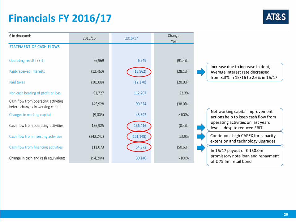
Financials FY 2016/17
€ in thousands2015/16 2016/17
Change
YoY
STATEMENT OF CASH FLOWS
Operating result (EBIT) 76,969 6,649 (91.4%)
Paid/received interests (12,460) (15,962) (28.1%)
Paid taxes (10,308) (12,370) (20.0%)
Non cash bearing of profit or loss 91,727 112,207 22.3%
Cash flow from operating activities
before changes in working capital145,928 90,524 (38.0%)
Changes in working capital (9,003) 45,892 >100%
Cash flow from operating activities 136,925 136,416 (0.4%)
Cash flow from investing activities (342,242) (161,148) 52.9%
Cash flow from financing activities 111,073 54,872 (50.6%)
Change in cash and cash equivalents (94,244) 30,140 >100%
29
Increase due to increase in debt; Average interest rate decreased from 3.3% in 15/16 to 2.6% in 16/17
Net working capital improvement actions help to keep cash flow from operating activities on last years level – despite reduced EBIT
In 16/17 payout of € 150.0m promissory note loan and repayment of € 75.5m retail bond
Continuous high CAPEX for capacity extension and technology upgrades
Net Working Capital Management
103
92 95
88
24
19.0%
15.6%
14.3%
11.6%
3.0%
2012/13 2013/14 2014/15 2015/16 2016/17
Net Working Capital development Net Working Capital as a percentage of revenues
€ in millions; % of revenue
Net Working Capital development
30

AT&S – Stock Profile
Listing: Vienna Stock Exchange,
Prime Standard
Indices: ATX Prime, WBI
Thomson Reuters (A): ATSV.VI
Bloomberg (A): ATS:AV
Record Date Annual General Meeting 26 June 2017
23rd Annual General Meeting 06 July 2017
Ex-Dividend Day 25 July 2017
Record Date Dividend 26 July 2017
Dividend Payment Day 27 July 2017
31
Financial Calendar Shareholder structure
# of shares outstanding 38.85m
Average daily volume: ~ 61,800 shares*
Performance YTD: +6.55%*
Dividend 2015/16: € 0.36 per share
Dividend yield: 2.8%
* 01/01/2017 – 30/04/2017
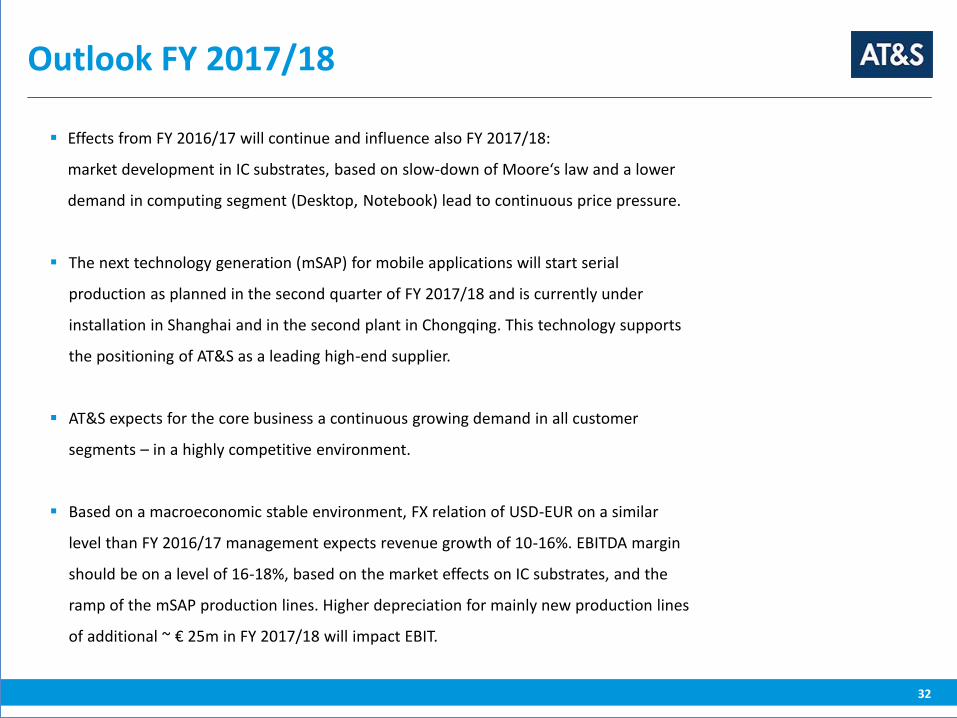
Outlook FY 2017/18
32
Effects from FY 2016/17 will continue and influence also FY 2017/18:
market development in IC substrates, based on slow-down of Moore‘s law and a lower
demand in computing segment (Desktop, Notebook) lead to continuous price pressure.
The next technology generation (mSAP) for mobile applications will start serial
production as planned in the second quarter of FY 2017/18 and is currently under
installation in Shanghai and in the second plant in Chongqing. This technology supports
the positioning of AT&S as a leading high-end supplier.
AT&S expects for the core business a continuous growing demand in all customer
segments – in a highly competitive environment.
Based on a macroeconomic stable environment, FX relation of USD-EUR on a similar
level than FY 2016/17 management expects revenue growth of 10-16%. EBITDA margin
should be on a level of 16-18%, based on the market effects on IC substrates, and the
ramp of the mSAP production lines. Higher depreciation for mainly new production lines
of additional ~ € 25m in FY 2017/18 will impact EBIT.

Overview of the transformation from a high-end PCB manufacturer to a high-end interconnect solutions provider:
Core Business New technologies and interconnect
solutions
Extended Technology Toolbox
Additional customers
Additional applications
More comprehensive positioning in the value chain
Mo
re t
han
AT&
S
+
This new positioning „More than AT&S“ is the foundation for returning back to profitability in FY 2018/19 with an EBITDA margin level based on mid-term guidance (18-20%).
Outlook beyond 2017/18
33

34
Company Overview
Strategy & Market
Annex
Financials
Table of Contents

AT&S Product Portfolio – I
ECP®: Embedded Component Packaging
IC substrates Substrate-like printed circuit boards
Embedded Component Packaging allows to embed active/passive components (e.g. wafer level dies) within the layers of a PCB – contributes to miniaturization.
IC substrates serve as interconnection platform with higher density (Line/Space < 15 micron) between semiconductors (Chips) & PCBs .
Substrate-like PCBs are the next evolution of high-end HDI PCBs with higher density: Line/Space < 30 micron.
Production site Leoben
Chongqing
Chongqing, Shanghai
Applications Devices such as smartphones, tablets, digital cameras and hearing aids
High-end processors for Computer, Communication, Automotive, Industrial
Mobile applications like wearables
35

AT&S Product Portfolio – II
HDI any-layer printed circuit
boards
HDI microvia printed circuit boards – high density interconnect
Multilayer printed circuit boards
Double-sided printed circuit boards
IMS printed circuit boards – insulated
metal substrate
Further technological enhancement to HDI microvia: All electrical connections in HDI any-layer boards consist of laser-drilled microvias. Advantage: further miniaturization, and higher performance and reliability. AT&S produces HDI any-layer in 4 to 12 layers.
HDI: high density interconnect, meaning laser-drilled connections (microvias). HDI is first step towards miniaturization. AT&S can produce 4-layer laser PCBs up to 6-n-6 HDI multi layer PCBs.
Found in almost every area of industrial electronics. AT&S produces printed circuit boards with 4 to 28 layers, in quantities from individual prototypes to small batches and mass production.
Used in all areas of electronics. AT&S focuses on double-sided printed circuit boards with thicknesses in the range of 0.1-3.2mm.
IMS: insulated metal substrate. Primary function: heat dissipation for use mainly with LEDs and power components.
Production site Shanghai
Shanghai, Leoben
Leoben, Nanjangud, Fehring
Fehring, Nanjangud
Fehring
Applications Smartphones, Tablets, Notebooks
Mobile phones and nearly all electronic applications including automotive (navigation, infotainment and driver assistance systems)
Used in all electronic applications including touch panels, and in products ranging from aircraft to motorcycles, from storage power plants to solar arrays
Primarily industrial and automotive applications
Lighting industry
36

AT&S Product Portfolio – III
Flexible printed circuit boards
Semi-flexible printed circuit boards
Rigid-flex printed circuit boards
Flexible printed circuit boards on aluminum
AT&S patented technologies
Used to replace wiring and connectors, allowing for connections and geometries that are not possible with rigid printed circuit boards.
More limited bend radius than flexible printed circuit boards. The use of a standard thin laminate makes them a cost-effective alternative.
Combine the advantages of flexible and rigid printed circuit boards, yielding benefits for signal transmission, size and stability.
Used when installing LEDs in car headlights, for example, where the printed circuit board is bonded to an aluminum heat sink to which the LEDs are then attached.
Production site Ansan, Fehring
Fehring
Leoben, Ansan
Ansan
Applications Nearly all areas of electronics, including measuring devices and medical applications
Automotive applications
Industrial electronics, such as production machines and industrial robots
Lighting, automotive, building lighting
ECP®: Embedded Component Packaging ECP® is a patented AT&S packaging technology used to embed active and passive electronic components in the inner layers of a printed circuit board. ECP® technology is used in ever smaller, more efficient and more powerful devices, such as smartphones, tablets, digital cameras and hearing aids. Production site: Leoben
2.5D® Technology Platform Combines mechanical and electronic miniaturization, and enables partial reduction of the thickness of a circuit board. Advantage: populated assemblies have a thinner profile. Can be also used to make cavities in the printed circuit board, e.g. for acoustic channels. Major application for this technology is the 2.5D® rigid-flex printed circuit board, a lower cost alternative for flex-to install applications. Production sites: Leoben, Shanghai
37
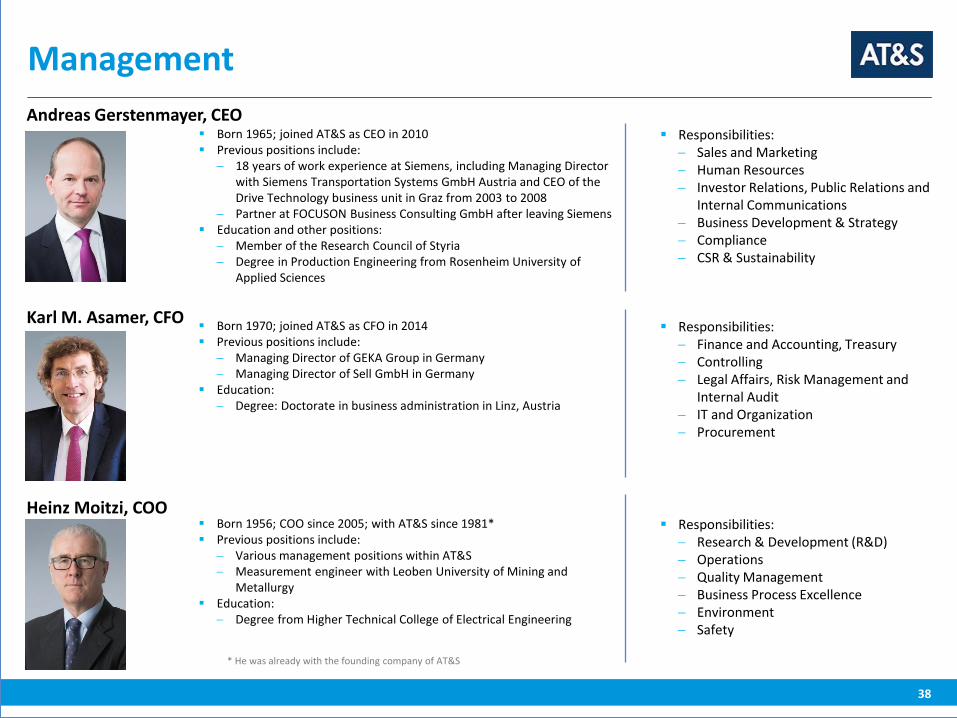
Management
Andreas Gerstenmayer, CEO Born 1965; joined AT&S as CEO in 2010 Previous positions include:
18 years of work experience at Siemens, including Managing Director with Siemens Transportation Systems GmbH Austria and CEO of the Drive Technology business unit in Graz from 2003 to 2008
Partner at FOCUSON Business Consulting GmbH after leaving Siemens Education and other positions:
Member of the Research Council of Styria Degree in Production Engineering from Rosenheim University of
Applied Sciences
Heinz Moitzi, COO Born 1956; COO since 2005; with AT&S since 1981* Previous positions include:
Various management positions within AT&S Measurement engineer with Leoben University of Mining and
Metallurgy Education:
Degree from Higher Technical College of Electrical Engineering
Karl M. Asamer, CFO Born 1970; joined AT&S as CFO in 2014 Previous positions include:
Managing Director of GEKA Group in Germany Managing Director of Sell GmbH in Germany
Education: Degree: Doctorate in business administration in Linz, Austria
* He was already with the founding company of AT&S
Responsibilities: Sales and Marketing Human Resources Investor Relations, Public Relations and
Internal Communications Business Development & Strategy Compliance CSR & Sustainability
Responsibilities: Finance and Accounting, Treasury Controlling Legal Affairs, Risk Management and
Internal Audit IT and Organization Procurement
Responsibilities: Research & Development (R&D) Operations Quality Management Business Process Excellence Environment Safety
38

Milestones in the Group’s history
1987 Founding of the Group, emerging
from several companies owned by
the Austrian State Owned
Industries.
1994 Privatization and acquisition
by Messrs. Androsch,
Dörflinger, Zoidl.
1999 Initial public offering on Frankfurt Stock Exchange
(„Neuer Markt“). Acquisition of Indal Electronics
Ltd., largest Indian printed circuit board plant
(Nanjangud) – today, AT&S India Private Limited.
2002 Start of production at new Shanghai
facility – one of the leading HDI
production sites in the world.
2010 Start of production
at plant II in India.
2009 New production direction: Austrian
plants produce for high-value niches
in the automotive and industrial
segment; Shanghai focuses on the
high-end mobile devices segment.
2008 AT&S changes
to Vienna Stock
Exchange. 2006 Acquisition of Korean
flexible printed circuit
board manufacturer,
Tofic Co. Ltd. – today,
AT&S Korea Co., Ltd.
2015 AT&S again achieves record high sales and earnings for
financial year 2014/15 and decides to increase the investment
program in Chongqing from € 350m to € 480m.
2011 Construction starts on new
plant in Chongqing, China.
Capacity increase in
Shanghai by 30%.
2013 AT&S enters the IC substrates
market in cooperation with a
leading manufacturer of
semiconductors.
2016 AT&S starts the serial production
of IC substrates at the plant in
Chongqing.
39

Five core dimensions of sustainability within AT&S
Energy and carbon footprint
Water
AT&S – a learning organization
Resources
Thinking ahead – shaping the future
CSR gains importance in long term success Improving efficiency Motivated and qualified staff
CSR as a key to sustainable business success
The importance of sustainability is rising within:
Authorities (basis for securing operation licenses)
Customers (relevant for placing orders)
40

AT&S saves CO2 and Water…
Sustainability – Figures and Fields of Action
AT&S aims to minimize its environmental footprint by reducing the CO2 emissions per m2 PCB attributable to production processes by 5% a year.
AT&S aims to reduce the Group‘s annual fresh water consumption per m2
PCB by 3%.
** in liters per sqm weighted PCB
* in kg CO2 per sqm weighted PCB
41
51.0 50.7 49.0
50.7
55.7
2012/13 2013/14 2014/15 2015/16 2016/17
Carbon footprint*
834.7 783.9
734.0 718.6 739.5
2012/13 2013/14 2014/15 2015/16 2016/17
Freshwater consumption**

Visit: www.ats.net; Twitter @AT&S IR_PR; YouTube AtundS
AT&S – First choice for advanced applications
IR contact: Elke Koch Fabriksgasse 13, 8700 Leoben/Austria Tel: +43 3842 200 5925 Mobile: +43 676 8955 5925 Fax: +43 3842 200 15909 [email protected] www.ats.net
42

Disclaimer
This presentation is provided by AT & S Austria Technologie & Systemtechnik Aktiengesellschaft, having its headquarter at Fabriksgasse 13, 8700 Leoben, Austria
(“AT&S”), and the contents are proprietary to AT&S and for information only.
AT&S does not provide any representations or warranties with regard to this presentation or for the correctness and completeness of the statements contained therein,
and no reliance may be placed for any purpose whatsoever on the information contained in this presentation, which has not been independently verified. You are
expressly cautioned not to place undue reliance on this information.
This presentation may contain forward-looking statements which were made on the basis of the information available at the time of preparation and on management‘s
expectations and assumptions. However, such statements are by their very nature subject to known and unknown risks and uncertainties. As a result, actual
developments, results, performance or events may vary significantly from the statements contained explicitly or implicitly herein.
Neither AT&S, nor any affiliated company, or any of their directors, officers, employees, advisors or agents accept any responsibility or liability (for negligence or
otherwise) for any loss whatsoever out of the use of or otherwise in connection with this presentation. AT&S undertakes no obligation to update or revise any forward-
looking statements, whether as a result of changed assumptions or expectations, new information or future events.
This presentation does not constitute a recommendation, an offer or invitation, or solicitation of an offer, to subscribe for or purchase any securities, and neither this
presentation nor anything contained herein shall form the basis of any contract or commitment whatsoever. This presentation does not constitute any financial analysis
or financial research and may not be construed to be or form part of a prospectus. This presentation is not directed at, or intended for distribution to or use by, any
person or entity that is a citizen or resident or located in any locality, state, country or other jurisdiction where such distribution, publication, availability or use would be
contrary to law or regulation or which would require any registration or licensing within such jurisdiction.
43