Embed Size (px)
Citation preview
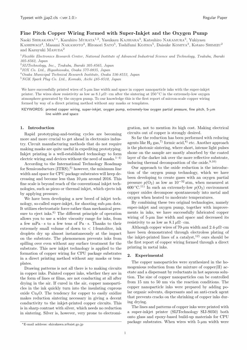
Typeset with jjap2.cls <ver.1.0> Regular Paper
Fine Pitch Copper Wiring Formed with Super-Inkjet and the Oxygen Pump
Naoki Shirakawa1 ∗, Kazuhiro Murata1,2, Yasukazu Kajihara3, Katsuhiro Nakamura3, YukiyasuKashiwagi4, Masami Nakamoto4, Hironori Sato5, Toshifumi Kojima5, Daisuke Komiya2, Kotaro Shimizu2
and Kazuyuki Masuda2
1Flexible Electronics Research Center, National Institute of Advanced Industrial Science and Technology, Tsukuba, Ibaraki305-8562, Japan2SIJTechnology, Inc., Tsukuba, Ibaraki 305-8565, Japan3IOX Co. Ltd., Higashiosaka, Osaka 577-0835, Japan4Osaka Municipal Technical Research Institute, Osaka 536-8553, Japan5NGK Spark Plug Co. Ltd., Komaki, Aichi 485-8510, Japan
We have successfully printed wires of 5-µm line width and space in copper nanoparticle inks with the super-inkjetprinter. The wires show resistivity as low as 8.1 µΩ · cm after the sintering at 250 C in the extremely-low oxygenatmosphere generated by the oxygen pump. To our knowledge this is the first report of micron-scale copper wiringformed by way of a direct printing method without any masks or templates.
KEYWORDS: printed copper wiring, super-inkjet, oxygen pump, extremely-low oxygen partial pressure, fine pitch, 5-µmline width and space
1. Introduction
Rapid prototyping-and-testing cycles are becomingmore and more crucial to get ahead in electronics indus-try. Circuit manufacturing methods that do not requiremaking masks are quite useful in expediting prototyping.Inkjet printing is a well-established technology to formelectric wiring and devices without the need of masks.1–4)
According to the International Technology Roadmapfor Semiconductors (ITRS),5) however, the minimum linewidth and space for CPU package substrates will keep de-creasing and become less than 10 µm around 2016. Thisfine scale is beyond reach of the conventional inkjet tech-nologies, such as piezo or thermal inkjet, which ejects inkby applying pressure.
We have been developing a new breed of inkjet tech-nology, so-called super-inkjet, for shooting sub-µm dots.It utilizes electrostatic force rather than mechanical pres-sure to eject inks.6) The different principle of operationallows you to use a wider viscosity range for inks, froma few mPa · s to a few tens of Pa · s. Thanks to theirextremely small volume of down to < 1 femtoliter, inkdroplets dry up almost instantaneously at the impacton the substrate. The phenomenon prevents inks fromspilling over even without any surface treatment for thesubstrate. This new inkjet technology is applied to theformation of copper wiring for CPU package substratesin a direct printing method without any masks or tem-plates.
Drawing patterns is not all there is to making circuitsin copper inks. Painted copper inks, whether they are inthe form of lines or films, are not conducting at all afterdrying in the air. If cured in the air, copper nanoparti-cles in the ink quickly turn into the insulating cuprousoxide Cu2O. The tendency for copper to easily oxidizemakes reduction sintering necessary in giving a decentconductivity to the inkjet-printed copper circuits. Thisis in sharp contrast with silver, which needs no reductionin sintering. Silver is, however, very prone to electromi-
∗E-mail address: [email protected]
gration, not to mention its high cost. Making electricalcircuits out of copper is strongly desired.
So far the reduction has been performed with reducingagents like H2 gas,7) formic acid,8) etc. Another approachis the photonic sintering, where short, intense light pulsesshone on the sample are mostly absorbed by the coatedlayer of the darker ink over the more reflective substrate,inducing thermal decomposition of the oxide.9,10)
Our approach to the oxide reduction is the introduc-tion of the oxygen pump technology, which we havebeen developing to create gases with an oxygen partialpressure p(O2) as low as 10−32 atm, when measured at600 C.11) In such an extremely-low p(O2) environmentcopper oxides decompose spontaneously into metal andoxygen when heated to moderate temperatures.
By combining these two original technologies, namelysuper-inkjet and oxygen pump, together with improve-ments in inks, we have successfully fabricated copperwiring of 5-µm line width and space and decreased itsresistivity to as low as 8.1 µΩ · cm.
Although copper wires of 70-µm width and 2.4-µΩ ·cmhave been demonstrated through electroless plating ofthe inkjet-printed lines of a catalyst,12) ours should bethe first report of copper wiring formed through a directprinting in metal inks.
2. Experimental
The copper nanoparticles were synthesized in the ho-mogenious reduction from the mixture of copper(II) ac-etate and a dispersant by reductants in hot aqueous solu-tion. The size of copper nanoparticles can be controlledfrom 15 nm to 50 nm via the reaction conditions. Thecopper nanoparticle inks were prepared by adding po-lar organic solvents, dispersants and an anti-crack agentthat prevents cracks on the shrinking of copper inks dur-ing drying.
The lines and patterns of copper inks were printed witha super-inkjet printer (SIJTechnology SIJ-S050) bothonto glass and epoxy-based build-up materials for CPUpackage substrates. When wires with 5-µm width were
1

2 Accepted for Jpn. J. Appl. Phys.
Fig. 1. Copper nanoparticles obtained in this study. The particlesize distributes around 15 nm.
drawn, nozzles with 3–4 µm inner diameters were used.Larger nozzles were usable for line widths > 50 µm.
The samples were then sintered at 250 C in the ni-trogen atmosphere with an extremely-low p(O2) for sev-eral hours. The p(O2) is measured with the oxygen sen-sor heated to 600 C. We have to keep in mind that thep(O2) should vary with temperature. The typical p(O2)during the sintering was 10−28 atm when the nitrogenwas sensed by the 600-C sensor.
The standard, DC four-probe method was used tomeasure line resistance of the copper wires. We used thelaser microscope (Keyence VK-9500) to measure theircross sections, which were used to calculate the volumeresistivity. The laser microscope was also used to takepictures of the printed patterns.
3. Results and discussions
A TEM photograph of the obtained copper nanopar-ticles is shown in Fig. 1. The particle size distributioncenters around 15 nm. The improvements in anti-crackagents were crucial in preventing cracks while the inkdried. The property of the anti-crack agent seemed tohave an impact also on the resistivity of the final prod-uct after sintering. The optimization is still going on.
Figure 2 shows the copper wires of 5-µm line widthand space, printed on the glass substrate. Another sam-ple (shown in the top panel of Fig. 3) was measured forits cross sectional shape and the standard deviation ofthe line width. The thickness of this sample was around1.4 µm. From 12 line widths measured in the photo-graph at an almost equal interval along the length ofthe wire, we estimate the line-width standard deviationas 0.28 µm.
In another example a pattern mimicking the wiring oftrue CPU package substrates was demonstrated on anepoxy substrate (Fig. 4). The line width here is 10µm.
The copper wires inkjet-printed on glass substrateswere then sintered in the extremely-low p(O2) atmo-sphere. The solid red line in the phase diagram of Fig. 5shows the boundary between CuO and metallic Cu inthe p(O2)–temperature plane. This line has been calcu-
Fig. 2. The photograph of copper wires with 5-µm line width andspace. The tick in the figure corresponds to 5 µm.
3.0
2.5
2.0
Hei
ght (
µm)
4846444240
Horizontal position (µm)
(b)
(a)
Fig. 3. (a) The photograph of a copper wire about which thestandard deviation of the line widths was measured. (b) A typicalcross sectional shape of the above sample.
Fig. 4. The photographs in different magnifications of a testwiring pattern resembling that of a true CPU package substrate.The substrate was made of the commercially-used build-up ma-terial.

Accepted for Jpn. J. Appl. Phys. 3
10-60
10-50
10-40
10-30
10-20
10-10
p(O
2) [
atm
]
600500400300200100
T [°C]
2CuO2Cu + O2 (g)
10-32
atm at 600°C
Expected behavior of p(O2)
Fig. 5. The phase diagram of Cu-O system. The red solid lineindicates the boundary between CuO and Cu metal in thep(O2)–temperature plane. The blue broken line shows the ex-pected behavior of p(O2) of the output gas of the oxygen pumpwhen the temperature varies.
lated by the software called HSC 5.1 from OutokumpuResearch Oy, Finland. Its calculation about the Cu-Osystem is based on the thermodynamic data compiled byKnacke et al.13) If the sintering condition is located belowthis line, CuO decomposes spontaneously and becomespure Cu. If the p(O2) of the gas generated by the oxygenpump is 10−32 atm at 600 C, the p(O2) is expected todecrease towards low temperatures as shown by the bluebroken curve. This means that our sintering condition isalways below the phase boundary, in favor of the metal-lic Cu, irrespective of temperature. We need, however,some level of thermal activation to facilitate especiallysintering rather than reduction. We thus needed to heatthe sample up to 250 C.
The resultant resistivity of the sample was 8.1µΩ · cmafter sintering in the above condition for several hours.The resistivity value is very good considering that thesample is a thin wire and not a wide-area film, which canprovide a lot of conducting paths between the measuringcontacts. Looking at the scanning ion microscope (SIM)image of the cross section of another sample (Fig. 6),however, we still see a lot of small grains and voids, whichis probably the cause of the higher resistivity than thatof pure bulk copper (1.7µΩ ·cm). We are working on thisissue and also on shortening the sintering process.
4. Conclusion
To print fine-pitch copper wiring using no masks ortemplates, we have adopted the super-inkjet printingtechnology. We have successfully printed copper wiringof 5-µm line width and space. As a necessary step of re-duction sintering, we have introduced the oxygen pumptechnology. Along with the aid of improvements in inks,
we have achieved a low resistivity of 8.1 µΩ · cm in theprinted thin wire of copper. We have made an impor-tant step towards the “manufacture on demand” of CPUpackage substrates in the near future.
Fig. 6. The SIM cross sectional image of a sample after reductionsintering. This sample was not the best and showed the resistivityof about 21 µΩ · cm.
Acknowledgment
This research is funded by the Innovation PromotionProgram/Research and Development for Nanotechnol-ogy and Advanced Materials Applications from the NewEnergy and Industrial Technology Development Organi-zation (NEDO), Japan.
1) J. Heinzl and C. H. Hertz: Adv. Electron. El. Phys. 65 (1985)91.
2) T. R. Hebner, C. C. Wu, D. Marcy, M. H. Lu and J. C. Sturm:Appl. Phys. Lett. 72 (1998) 519.
3) H. Sirringhaus, T. Kawase, R. H. Friend, T. Shimoda, M. In-basekaran, W. Wu and E. P. Woo: Science 290 (2000) 2123.
4) S. Roy: J. Phys. D: Appl. Phys. 40 (2007) R413 and referencestherein.
5) http://www.itrs.net/Links/2011ITRS/Home2011.htm6) K. Murata, J. Matsumoto, A. Tezuka, Y. Matsuba and H.
Yokoyama: Microsyst. Technol. 12 (2005) 2.7) Y. Lee and Y. Choa: J. Mater. Chem. 22 (2012) 12517.8) Y. Choi, J. Lee, S. J. Kim, D. Yeon and Y. Byun: J. Mater.
Chem. 22 (2012) 3624.9) N. Marjanovic, J. Hammerschmidt, J. Perelaer, S. Farnsworth,
I. Rawson, M. Kus, E. Yenel, S. Tilki, U. S. Schubert andR. R. Baumann: J. Mater. Chem. 21 (2011) 13634.
10) J. Perelaer, R. Abbel, S. Wunscher, R. Jani, T. van Lammerenand U. S. Schubert: Adv. Mater. 24 (2012) 2620.
11) K. Endo, N. Shirakawa, Y. Yoshida, S.-I. Ikeda, T. Mino,E. Gofuku, E. Suzuki: Jpn. J. Appl. Phys. 45 (2006) L393.
12) S. Fang, Q. Zhou, T. Kamakura, H. Kitahara, S. Ichikawa,M. Furusawa and S. Inoue: Proc. Int. Display Workshop ’07,2007, p. 713.
13) O. Knacke, O. Kubaschewski, K. Hesselman: ThermodynamicProperties Inorganic Substances (Springer-Verlag, Berlin,1991) 2nd. ed.