Embed Size (px)
Citation preview

Hard Drive Controller Lab Page 1
Final Technical Report
Instrumentation for Laboratory ImprovementNSF Grant DUE-9850821
Remote Distance Learning with FieldProgrammable Circuit Boards – a 21st
Century Approach to TeachingHeterogeneous Computer Hardware Design
J. F. McDonaldECSE Department &
Center for Integrated ElectronicsRensselaer Polytechnic Institute
Troy, New York 12181(518)-276-2919
eFAX (503)[email protected]
“LWL - The Laboratory without Lights”
Hard Drive Controller Lab Page 2
Executive Summary
In the 21st century more and more workers be telecommuting to work through internetconnections because of the extreme cost and increasing scarcity of fuel. Hence it willseem increasingly natural for students to telecommute to school. Remote DistanceLearning could also be seen to help long-term post secondary education, to provideeducational services to our men and woman in the services, to provide quality educationto minority and tribal students, and to assist an increasing market of single parents whowork at home. The biggest challenge in delivering such an education, however, would bein the incorporation of laboratory experiences. Laboratories by their very nature implyinteraction with the physical world through use of measurement instruments, forcing thestudent to understand and cope with measurement error and noise, stressing observationand analysis of these observations. In the laboratories for circuit design these interactionsalso involve perturbing the design under study in a quest to improve it, and then validatethe result. For remote distance learning this implies the ability to conceptualize designs,then implement them in a remote system, and then use remote instrumentation from hometo diagnose their creations. Throughout this process the environment of the actuallaboratory needs to be captured in a “virtual reality.” The actual laboratory could then belocated almost anywhere and literally operate in the dark. Hence the title of the effortbecame the “Laboratory without Lights” project or LWL, mimicking the Japanesereference to their highly automated factories as “Factories without Lights.”
A two-year NSF grant for $70,000 matched by Rensselaer funding of $70,000 wasrequested and awarded from the Instrumentation for Laboratory Improvement (ILI)program in 1998. This followed an earlier internally awarded $35,000 of funds from theRensselaer Strategic Initiatives program provided in 1997, to modernize a popular set ofcourses taught at Rensselaer. Leveraged with other funds, corporate donations anddiscounts, an ambitious program to provide students with an exciting new experience incomputer hardware design at Rensselaer was undertaken. The proposal was to modernizethe facilities and revamp the content of 35.477 Computer Hardware Design and itssuccessor 35.670 Advanced Computer Hardware Design so that they better reflect therapid changes in this field and assume a more prominent role in the new 4 x 4 ElectricalEngineering and Computer and Systems Engineering curricula, and accommodate theincreases in enrollment due to new Information Technology thrusts on the campus. Inaddition, this modernization effort provided an opportunity to explore ways to use newtechnology to permit remote distance learning in a course sequence whose entire claim topopularity was the “hands on” experience that it provided students in its laboratory.
In addition to the key NSF support, this project would not have been possible withoutgenerous grants and donations from Hewlett Packard, DEC/Compaq, NationalInstruments, APTIX, SUN, Annapolis Microsystems, Xilinx, Altera, IBM, VirtualComputing, and BIT. Continued support by NSF under its CRCD is acknowledged. TheILI proposal acted as an enabler for these numerous grants to coalesce successfully.

Hard Drive Controller Lab Page 3
A Short History of Computer Hardware Design Lab at Rensselaer
Computer Hardware Design (ECSE/35.477) has been a popular senior/junior/fifth-yearlevel course offering at Rensselaer with a proud history of teaching a variety ofchallenging digital design skills to students for nearly 28 years. These skills includecomputer interface design and computer hardware prototyping. The lab provided some ofthe first “hands-on” hardware design experience for ECSE and CS students. For most ofthese years the computer used for teaching these skills has remained the same, namely theDEC LSI-11. One can argue that basic computer design skills remain unchanged overthis period and hence why should it change? But the application arena in which theseskills get tested in real life changed at least a dozen times in the history of the class.Eventually change must occur.
The CHD lab was started in 1974 with the award of a Title VI HEW grant. From itsinception the lab focused on DEC hardware because DEC in the early days of the lab wasparticularly interested in education, and offered copious documentation to aid in teaching.In 1980 NSF awarded some high frequency plug in equipment and one new highfrequency oscilloscope. In 1990 the course received a major grant from DEC of threenew micro-VAX systems. These two systems can be seen in the lab prototyping stationin Figure 1 along with recent graduate Jason Bennett, (now employed at INTEL). It tooknearly two years just to convert one of the labs to the micro-VAX, since another problemfacing teachers is the shortage of TA support for new lab development, and so the coursestill depended partially on the LSI-11. Three of these prototyping stations wereeventually fielded for accommodating up to 9 students per three-hour lab slot. By timesharing the three stations over multiple lab meeting times, the equipment costs for the labwere kept reasonable, but there was a continuous cost of TA hours. This is madenecessary by institute rules on lab supervision for safety considerations. In addition a fulltime technician was required to maintain the equipment. One of the penalties of “handson” laboratory experience is “hands on destruction.”
A key parameter evaluating the relevance of the equipment offering in CHD lab has beenthe bandwidth or frequency of operation of its circuits and instruments. Although theLSI-11 is only a 1 MHz clock machine, many phenomena often require instruments thatperform at speeds well in excess of the computer’s clock rate when performing systemprototyping. For this reason one of the more beneficial offerings of the lab has been in itsoscilloscopes, counters and pulse generators. These permitted viewing “glitches” or“bugs” with substantially wider bandwidth than the basic clock rate. Often the casualobserver will not appreciate why such equipment is necessary. However, typically to seea good clock square wave one needs to be able to observe 9 odd harmonics of thefundamental, or 18 total harmonics. This means that a 1MHz computer really needs 18MHz of operating bandwidth. Similarly, a 300 MHz computer requires about 6 GHz todo the same! Equipment with this capability is extremely expensive, and is one reasonthat held back the modernization effort.

Hard Drive Controller Lab Page 4
Figure 1. Past History. Computer Hardware Design Prototyping Station used fornearly 28 years to teach basic digital systems design.
Although the lab managed to survive essentially on the same equipment for more than aquarter of a century, the skill set taught transcended the age of the instrumentation, or thegeneration of microprocessors in vogue in any given year, keeping interest in the coursehigh. This mitigated the effect of the aging of the equipment, but also helped with theruinous rate of change of microcomputer hardware, doubling in performance every threeor so years by Moore’s law. This is a testament to the generic nature of the skills taught.Students who have taken similar courses elsewhere, or even simpler courses within ECSEat Rensselaer, report that the skill set taught remains more ambitious in CHD. Studentscompleting CHD could claim to have designed and successfully prototyped a diskcontroller in a job interview, for example. This is a basic skill, which lends itself to longterm value for the student.
However, this still left the lab dependent on 10-30 year old technology. In recent years itbecame apparent that this situation was becoming unmaintainable, and was no longerpreparing the student for the modern design environment. Student complaints about theage of the equipment were chronic. Oscilloscopes in the lab shown in Figure 2 were alsoapproaching the same age, and replacement parts or repair become less tenable with eachpassing year. Other instruments in the lab were beginning to show wear.
Several scenarios were pursued to attempt to change the laboratory over to a MotorolaM68,000 based course due to the similarity of that microprocessor and the DEC LSI-11and the uVAX, but the Motorola printed circuit boards were not as rugged as the DEC

Hard Drive Controller Lab Page 5
pin-block assembly and as flexible as the DEC wire wrap technology. Eventually theeffort was put to one side since the older labs were very reliable, in spite of many 10’s ofthousands of board insertions and extractions, and wire wrap board stripping by thestudents. Pedagogically the UNIBUS standard and Q-BUS uVAX variations withstoodthe test of time. These bus standards taught students many important skills such asasynchronous design, and caus- effect diagnostic techniques.
Figure 2. More Past History. Thirty Year Tektronix Series 7000 Oscilloscopes, stillin use till last year.
Professors who teach laboratory-oriented courses at any school have become accustomedto the fact that money comes grudgingly to support labs over the years. Experienceshows that money becomes available for major modernization campaigns every 10 yearsor so. Simulation of systems can provide some relief, but actual hands-on experiencedemands real equipment.
Labs are popular with Rensselaer undergraduates, but lab equipment demands aresubstantial. Labs provide an important link between necessary abstract lecture conceptsand job related skills. However, Labs are loss-leaders in economic terms. Labs demandTA support, a large number of teacher contact hours, and technical support in addition toequipment and materials. Furthermore, the write-down time for depreciation in thecomputer area is extremely short, approximately 3 years. Hence, computer labs are veryseverely affected by the rapid advances in the field. Therefore, while there is a greatappeal to students to experience “hands-on” labs in their courses, the increase in lab or“lab-like” offerings has introduced many new economic demands.
Hard Drive Controller Lab Page 6
The key point to observe, however, is that most of the early equipment for ComputerHardware Design Lab came from funds obtained from NSF or HEW teaching equipmentprograms through vigorous proposal writing, with deep educational discounting ondemonstration sales models. The funding of the present grant came after 8 years ofpersistent continuous but unsuccessful proposal writing to ILI, in which the basicmessage remained the same, only the words were changed in small ways fromsubmission to submission. The last proposal almost did not get written but it is that “onelast try” that brings success. This is an important message for other future ILI proposalwriters who may become frustrated by repeated efforts to propose educationalinnovations about which they feel most deeply, only to face repeated rejection, withunfathomable or even conflicting reviewer comments. One must accept that the amountof money for this kind of work is apparently very scarce and heavily sought. Theconclusion is that one must pick objectives wisely with a long time horizon of at least 10years. If the ideas are good, eventually a program manager or reviewer will empathizewith the proposed theme and want to see it succeed. Once the basic award is obtained,one success follows another.
In the case of the present grant, its award encouraged the writing of additional proposalsleveraging NSF funding eight fold. NSF funding totaled $70,000 while the total value ofthe new laboratory equipment is $579,000. Fortunately the theme proposed to NSF forremote distance interactive lab learning coincided with corporate educational objectivesat important companies like HP, IBM, National Instruments and SUN.

Hard Drive Controller Lab Page 7
Recent Events
When the 1997 opportunities for Strategic Initiatives were presented at Rensselaer, awhite paper was prepared for support of Computer Hardware Design Lab and itscompanion second term course, Advanced Computer Hardware Design Lab. A newaward winning course format called the “Studio Format” had become the focus of muchof the internal funding at Rensselaer. The CHD lab was a traditional lab and not a studio.There was some concern at the time that a “non-studio” conventional lab would not farewell in the competition for these funds. Nevertheless, it was clear that this lab figuredimportantly in the ECSE/ECS/EE/CS course sequence discussions, and so a proposal wassubmitted. The proposal requested $35K of SI funds to purchase a rack mounted DECAlpha upgrade to replace the aging LSI-11 machines. The unit as it was anticipated isshown in Figure 2. Although the machine had chassis openings for up to 4 DEC Alphasonly one would be included. Three duplicates of this chassis were desired. The spirit ofthe layout of the DEC VME 2100 seemed especially well matched to the needs of the lab.
Figure 3. Rack Mountable Four-Way DEC Alpha 2100-200 Parallel Processor withIntegrated PCI/VME Card Rack
In the spring of 1997 needless to say, everyone was pleasantly surprised that the proposalto SI 1997 was approved for funding. Evidently the SI committee must haveacknowledged the importance of conventional labs, even in the studio environment. This

Hard Drive Controller Lab Page 8
was extremely reassuring pedagogically, and ultimately opened up a new line ofdevelopment which the school began to recognize, namely remote learning.
Using the $35,000 awarded by the SI, plus the $15,000 of funds from the PrincipalInvestigator’s Overhead Incentive account, another proposal was written. This proposalwas sent to DEC’s sponsored research in-kind equipment donation program. With thehelp of Stan Strauss, and an internal RPI alumnus contact at DEC by the name of BjornZetterlund, DEC decided to match the RPI funds with an additional $170.485, by creatinga project with DEC contract number US-006297. The total value of the DEC Alphas thenwas $219,412. Hence the RPI contribution of $35,000 was leveraged by a factor of 6.2.In the end DEC was unable to deliver on some of the boards in the grant, and other lessexpensive boards were used reducing the grant value somewhat to $204K, but still a veryimpressive first return on the SI investment, and helped set the stage for the ILI proposal.
The DEC grant ended up giving the lab three entirely new racks with Alpha 4000/5-300computers, VME cages, and PCI interfacing capability. This is shown in Figure 3. TheDEC processors actually are dual Alphas, with two parallel processors, on each on twoprocessor boards, in each chassis. This makes CHD lab the first undergraduate lab toexpose students to parallel processing in a hardware prototyping environment.Furthermore the processors have an upgrade path from 300 MHz all the way up to 1.6GHz clock rates when they become available (800MHz exists already in DEC’s researchlabs). Of course more money would be required to keep modernizing these stations, butat least the incremental path is there.
An important difference about the Alpha from its predecessors is that it came with arather large amount of disk storage capability and a ULTRIX operating system thatpermitted students to log onto these stations from remote locations, and run variousprograms. This would prove important in what was to follow.
Note, however, that the very success of this venture to upgrade the computer used inCHD lab placed more stress on the existing oscilloscopes and logic analyzers in the labwhich had a typical bandwidth of only 500 MHz (one scope managed 1 GHz).

Hard Drive Controller Lab Page 9
Figure 4. Alpha 4000/300-5 Processor with Integrated PCI/VME Card Rack.Older Rack is Shown to the Right. The system is not open-face as shown in Figure
3, but in the LWL this is no longer as important as in the past.

Hard Drive Controller Lab Page 10
This grant means that the Computer Hardware Lab now has three 300MHz dualprocessor, dual superscalar 4000/5-300 microcomputer systems. Each of the systems willsupport up to 4 (with future upgrades) parallel processors that can communicate witheach other over a 300 MHz Synchronous Microprocessor Bus (SMB). Each of theseparallel processor cages will come equipped with two of the two processor boardsinitially. Each processor card in the cage will have its own 4.3 GB disk drive, and 128MB of 300 MHz memory. The 4 way parallel processor systems will be housed in onerack, specially integrated to an open face PCI/VME card cage providing capability forstudents to put cards out on card extenders, and view system signals. The fully integratedsystem also provides conventional double width SCSI, and 10BaseT interfacing standardsso the three rack mounted systems can be on the network with contiguous ground andpower supply connections for greater noise immunity. The 4000 series VAX wasselected among several alternatives for the upgrade capabilities presented by this modelto permit future board upgrades. Board upgrades could eventually take the systems toclock frequencies as high as 1. GHz. The original model we were interested in, namelythe VME 2100 rack mounted assembly only worked to 200 MHz clock rates and wasbeing discontinued, so there would have been no upgrade path for the future. Clearly, the4000 series was the superior machine.
The purchase order for this equipment against the supporting accounts was issued asRequisition 66624. The equipment for the main processors was received from DECaround January of 1998. However, many of the boards required for the VME and PCIfeatures took longer to be delivered, and in the end DEC reported to us that the64 bitwide VME to PCI bridge card we had ordered simply did not work. Rather than facelengthy delays this was downgraded to 32-bit width. This resulted in a large reduction inthe value of the grant, since 64-bit width bridging cost $12K per board. In exchange forour flexibility on the bit width, DEC compensated by offering three unusual boards calledPamettes. This change in the grant was the second important step along the path to theLWL.
These Pamette cards opened a new line of thinking on where the lab would go in thefuture, taking it even farther than had been expected or anticipated in the SI $35K grant.These three boards would begin to make the connection to remote learning possible.
Interestingly, the DEC grant was not primarily for education. DEC did not have aneducational program in 1997. The grant was for support of research for parallelprocessing in computing parasitics of interconnections on a chip, a part of the CAISTSRC initiative. The fact that the same machines could be used for teaching seemedirrelevant to DEC, but made it possible to provide for both a research and teachinginitiative. This is another testament to the concept of “balanced mode” teaching in whichboth research and teaching are brought into harmony with each other’s objectives, andcomplement each other rather than compete with each other. It is very much in keepingwith other research agendas in the Center for Integrated Electronics, where this particularteaching lab is located. It also reflects the point of view of the principal investigator forthe project.

Hard Drive Controller Lab Page 11
A HP Generous Donation -
Complementing this exceptional DEC grant, one 500 MHz HP 1660 logic analyzer wasdonated by Hewlett Packard as a part of another proposal. Eventually the lab would haveneeded two more of these analyzers, but the donation of one with no matching funds wasalso very favorable. This logic analyzer came only a few years after HP awarded the laba single HP 16500 logic analyzer. This gave the lab a choice of which analyzer todeploy in the three test stations.
Armed with no particular assurance of success, a proposal was made verbally toProfessor Bill Jennings, Chairman of ECSE, to approach HP for the oscilloscopesrequired for modernization of the CHD lab. The TEKTRONIX 7000 series mainframeswere 25 years old. Working with Professor Ed Maby, (who had previous success inobtaining such grants from HP), a proposal was submitted to HP for the oscilloscopes.During the development of the proposal the dollar amount that was encouraged fromvarious sources permitted a request for not only the three oscilloscopes, that were badlyneeded, but also two additional logic analyzers. The question was which of the tworecently donated analyzers to pick for replication.
Figure 5. The HP 1998 Donation is shown.It includes a HP Infinitum Oscilloscope and HP 16,500 Logic Analyzer. Three of
each system was donated.

Hard Drive Controller Lab Page 12
The infinitum oscilloscopes were distinguished as all having two channels of 4 GHzperformance, almost enough to see a crisp 300 MHz clock! The HP16,500 logicanalyzers provided 16 channels at 4 GHz and 100 channels at 500 MHz.
A Winning NSF ILI Grant after Eight Unsuccessful Years of Trying-
The success of the SI grant with its companion DEC award, and the anticipated successof the HP Oscilloscope and Logic analyzer donations helped create an air of optimism inthe fall of 1997. Armed with this enthusiasm, the CHD lab team, including ProfessorMcDonald, technician Steven Nicholas, and adjunct professor Russ Kraft began tospeculate about the possibility of other sweeping modernization in the lab. At the sametime the 1998 SI agenda shifted towards an entirely new direction, namely remotedistance learning. The award of the DEC pamette cards helped shift the thinking of thegroup. The Pamette is a card that makes it possible for the lab to shift toward remotedistance learning. The student can bring designs into the Pamette over the network andinstantiate them on a card that can be operated by the Alpha’s ULTRIX operating system,a system that is extremely robust.
Matching funds from ECSE department in the amount of $10,000 was actually notrequired for obtaining the DEC grant. As a result, this amount was held-over, asmatching moneys for additional upgrades needed by the lab. This was used as part of thematch for resubmitting an ILI proposal. This proposal was in its eighth year of rejectionby NSF. However, in the earlier submissions the proposal sought equipment that wasthought to be so basic as to reveal a lack of financial commitment to the lab at the homeinstitution. This burden dragged the proposal down every time it was submitted, despitemany excellent ratings over the years. However with the donations from DEC and HP,the ILI could focus its budget on the innovations sought. This involved reconfigurablecomputing.
The high ratings from the reviewers in the past for the ILI proposal were due to anovel technical innovation which ultimately can make the lab into one which can betaken from a remote location using only a home PC computer and some associatedcommonly available software, NETSACAPE or IE, and a telnet interface. Thisinnovation would ultimately make it possible for students to design things at home andenter the lab electronically and test their designs, not by simulation, but by use of actualhardware. This opened the door to placing spin on the proposal that emphasized remotedistance learning, which permitted a partial award of the ILI in its last year ofresubmission of $140,000 [$70,000 from NSF, $70,000 from RPI].
The “Lab without Lights” -
The NSF ILI proposal presented a concept coined by Dean Lester Gerhardt termed the“Lab without Lights.” This phrase was meant to mimic the Japanese concept of highlyautomated “Factories without Lights.” Students would be able to automate many tasksthat currently demand a lot of manual, error prone work, implementing designs. This

Hard Drive Controller Lab Page 13
labor tends to overwhelm the students in the present lab, with activities that involve littlethinking, and to introduce faults associated with the process of prototyping in theprevailing medium, namely wire wrap cards.
For nearly the entire 28-year history of CHD students laboriously drafted or drew logicdiagrams, and board layouts by hand, and then came into the lab to wire up the solutionsand test them. This process is called prototyping, and it is commonplace in industry towirewrap a prototype board before making a commitment to printed circuit boardmanufacturing. This process tied up valuable lab time because the equipment to wire theboards, in fact even the wire, were only available in the lab. Figures 6 and 7 show theW9301 wire wrap card as seen from the top and bottom. Figure 7 gives some feeling forthe amount of wiring involved. The wire wrap tools were expensive and so most of thatactivity had to be conducted during lab hours with an expensive TA watching. Wheneveran error was found, wire had to be stripped on the board and the changes retested.
Figure 6. DEC W9301 Standard Wire Wrap Board. Shown from the top or “chip”Side

Hard Drive Controller Lab Page 14
Figure 7. DEC W9301 Standard Wire Wrap Board. Shown from the bottom orWire Wrap Side.
A new concept appeared during the early 1990’swhich creates the opportunity to relievestudents from the burden of having to perform all the wiring associated with theprototyping activity. This concept is called reconfigurable computing. Reconfigurablecomputer hardware consists of use of electronic switches to route signals between variousdigital resources. These electronic switches are reprogrammable, permitting students totry wiring different designs by simply changing the state of these switches. In effect thestudent can wire up a board, and even design their own chips using this state of the artconcept. Three particular companies figure importantly in this field of reconfigurablecircuits. The first is Xilinx, the second is Altera, and the third is Aptix. Xilinx and Alteramake chips called Field Programmable Gate Arrays or FPGA’s. Altera pioneered takingthis concept to the circuit board level producing something called a Field ProgrammableCircuit Board of FPCB. As it turned out several past graduates of the CHD lab workedfor APTIX. The Xilinx and Altera chips are shown in Figures 8 and 9 on fixed wiringprinted circuit boards or PCB’s. These permitted students to load the FPGA’s on theseboards while in the labs with configuration bits generated using CAD or Computer AidedDesign tools made available by Xilinx and Altera. Loading the switches wasaccomplished using a CAD utility program that downloaded the configuration bits intothe FPGA on the board, implementing a prototype design in real (not simulated)hardware.

Hard Drive Controller Lab Page 15
Figure 8. Xilinx mini-Prototype Card showing Two Xilinx Field ProgrammableGate Array Chips, the XC3090, and the XC4010. A small conventional wire wraparea is shown to the right. Most of the wiring is programmed into the Xilinx chipsautomatically through electronic switches inside the chip.
Figure 8. This shows an Altera mini-Prototype Card showing Two Altera FieldProgrammable Gate Array Chips, the 4K, and the 10K. A plug to download the
configuration switch settings (millions of them) is shown at the top

Hard Drive Controller Lab Page 16
The information for configuring these integrated circuits is in essence the designas conceptualized by the student. Here again enormous strides have been made. Lengthydrafting exercises with pencil and paper to create designs can be replaced bycomputerized drafting aids. Many advantages accrue from this form of design. For onething the diagrams created can be cut-and-pasted into WORD documents discussing thedesign, making documentation of the design easier and cleaner. PC based inexpensiveComputer Aided Design (CAD) tools have only this year become available which assistin this drafting, so the design can be conducted at home. Furthermore, simulation can beconducted with pieces of the design also at home, providing at least a partial virtualverification of the design prior to entering the lab. The student still at this stage had toenter the lab to use instruments and downloading cables.
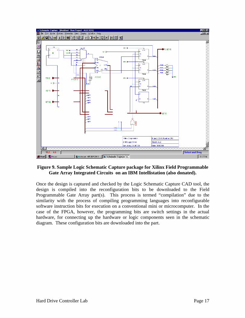
One particularly awkward aspect of design which has held CHD lab back fromentering the 64 bit microprocessor era, is the headache of wiring up 64 bit data paths, atedious and repetitive task with little educational value when conducted with a wirewrapboard such as the W9301. This single difficulty more than any other has held back thecourse from converting to new 64 bit and 128 bit architectures such as the DEC Alpha.However with the advent of the new CAD logic schematic capture drafting tools itbecomes possible to work with bus or “fat wire” drafting. By merely drawing a fat wireonce in the circuit diagram, the program interprets this as wiring up automatically all ofthe wires in the bundle. This is illustrated with the Xilinx logic schematic capturepackage shown in Figure 9 here below. Note the darker, red “fat wires.” In this case thefat wires only represent a 4 bit wide bus, but the idea is clear.
Hard Drive Controller Lab Page 17
Figure 9. Sample Logic Schematic Capture package for Xilinx Field ProgrammableGate Array Integrated Circuits on an IBM Intellistation (also donated).
Once the design is captured and checked by the Logic Schematic Capture CAD tool, thedesign is compiled into the reconfiguration bits to be downloaded to the FieldProgrammable Gate Array part(s). This process is termed “compilation” due to thesimilarity with the process of compiling programming languages into reconfigurablesoftware instruction bits for execution on a conventional mini or microcomputer. In thecase of the FPGA, however, the programming bits are switch settings in the actualhardware, for connecting up the hardware or logic components seen in the schematicdiagram. These configuration bits are downloaded into the part.

Hard Drive Controller Lab Page 18
Figure 10. Reconfigurable Wire Routing inside the Xilinx FPGA Produced by theCAD Tool shown in Figure 9.
Originally the concept was presented to NSF as a convenience for the student, who wouldactually program the reconfigurable wiring from the lab. This would have then requireduse of lab instruments to view various signals to diagnose the correctness of the designs.However, several independent develoments have converged to transform this process ofprototyping new systems into something which can be performed entirely at home. First,the new HP donations to the lab all involved something called an HPIB (or IEEE 488)standard instrument bus system connections. These bus connections made eachinstrument readable by a computer. However, the computer had to be in the lab.
The FPGA is not only a convenient technology to use for prototyping system designs inCHD but an emerging powerful technology for computing hardware that can bereconfigured rapidly to adapt to the needs of a given environment. For example FPGA’scan be configured as image compression engines with a certain resolution, and simplyreconfigured for a different resolution, or even a completely different function.Reconfiguration times are typically in the 10 ms range, but special versions canreconfigure in a few nanoseconds. IBM developed the Power PC architecture usinghardware emulation with these chips.

Hard Drive Controller Lab Page 19
Figure 11. Zoom in on a section of Figure 10 Showing More Details of the Wiringwhich is now completely automated (i.e. students are now completely freed of the
burden of wiring these connections.
National Instruments made a donation in 1998 to Rensselaer Polytechnic Institute forblanket use by its undergraduates of a software client which made it possible to viewIEEE 488 compatible instruments remotely. The client worked best with an instrumentrack called a PXI sold by National. With this instrument it formally becomes possible fora student to view the instruments in the lab at home on an IBM compatible PC. In factwith appropriate Viewer software, it became possible to even interact with theseinstruments from other platforms.
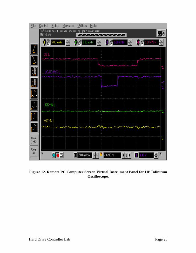
Fortunately for Rensselaer, the two HP instruments donated to CHD lab, the infinitumoscilloscope, and the 16,500 logic-analyzer already have LabVIEW virtual instrumentdisplays developed by National Instrument. This means that a student using theLabVIEW client on their home PC will be able to view instrument panels, change controlpanel settings, and select different signals to analyze. Figure 12 shows the consoledisplay for the HP infinitum oscilloscope. Both the infinitum and the HP 16,500 possessK6 AMD microprocessors, and run their instrument displays under Windows 95, so thematch to the LabVIEW environment is very good.
Hard Drive Controller Lab Page 20
Figure 12. Remote PC Computer Screen Virtual Instrument Panel for HP InfinitumOscilloscope.

Hard Drive Controller Lab Page 21
The DEC/Compaq Pamettes
In the middle of the negotiations with DEC the company was reorganized and bought outby Compaq. However a legacy of the earlier DEC corporate European structure was aconsiderable grant to several French universities to develop a card that would attach tothe DEC Alpha called the DEC Pamette. This card shown in figure 13.
Figure 13. DEC/Compaq PCI-64 Pamette Card showing 4 Xilinx 4028 FPGA’s,64b x 32K SRAM on lower left of card and 32 b x 64MB of DRAM DIMM inserts onthe lower right. Flexprint cable connections to the center of the card present an I/O
interface for the student (unfortunately unbuffered).
The 3 DEC/Compaq Pamettes offered significant improvements over the smaller Xilinxand Altera cards since the latter did not offer direct UNIX access, and offered only alimited amount of card memory. With the Pamette direct telnet connections permittedloading any of the 4 on-board 4028 Xilinx chips remotely using DEC provided boardmanagement software tools. On the pamette were slots for up to 32 bits of 64 MBmemory, and 64 bits by 32K of SRAM memory. Now the student had access to a gatecapacity of about 100,000 gate equivalents, as well as some DRAM and SRAM. Thisearly donation provided an opportunity to develop one of the first LWL labs, attached asan appendix to the end of this report. By clicking on any of the hot URL lines in that textother documents can be obtained The Pamette also provided a passageway to discuss thePCI bus as well as other buses (IDE in this case).
Remaining deficiencies at this point were lack of access to VME bus standards. DECgenerously provided access to the bus chassis by donating a BIT3 cage and PCI to VMEbridge card set, but this was for 32 bit VME only. Still remaining was the problem ofproviding student access to the VME bus signals for design purposes. Providing access

Hard Drive Controller Lab Page 22
to asynchronous bus signal design was one of the objectives of preserving older materialof merit from the predecessor course.
The ILI and the VME
One of the first possibilities that presented itself when the ILI grant was awaded was theextension of the results obtained on the DEC/Compaq grant for the PCI bus to the VMEbus. A special grant from Annapolis brought the price per board to $13,900 and animportant feature of the DEC grant was then realized, namely the BIT3 VME rackbecame remotely accessible. The Annapolis WidStar VME card also brought three V300Vertex Xilinx parts to the lab, the first such parts. The WildStar VME card is shown inthe DEC donated BIT3 VME crate in the Alpha six foot rack in Figure 14.
Figure 14. Annapolis Wild Star Vertex VME card [XCV400-4s WILDSTAR™ 6UVME, Model WS/XCV400-4V/2 2 MByte Memory] shown in the Dec/Compaq
ALPHA rack BIT3 VME Chassis.

Hard Drive Controller Lab Page 23
National Instruments Grant
One of the companies working on remote access to instrumentation is NationalInstruments. In addition to numerous specialized digital or analog input/output modules,National Instruments provides a rack mountable box called the PXI which makes itpossible to attach to any collection of HPIB or IEEE 488 bus compatible instruments. NIhas created software tools to create visual virtual instrument representations on computerscreens, including making these visible at remote internet PC’s, in some cases making itpossible to visualize data or capture it in a form not possible on the native instrumentalone. More importantly the HPIB bus provides a natural “fire wall” beyond whichinternet adversaries cannot reach to spread viruses or create other problems. Many of theHP supplied instruments are set up extremely well to permit access to the instrumentsdirectly over the web, but they are vulnerable to students exercising even the most basicdisk utilities, some of which could erase the instrument’s copy of the operating system.

Hard Drive Controller Lab Page 24
Figure 15. National Instruments PXI-1000 Remote Instrumentation Module.The PXI box itself is vulnerable to virus attack so internet security is important for itsuse, but it is also easier to do a clean system load on the PXI box than on the HPinstruments themselves since certain useful ports such as USB and SCSI for backup andrestore media were not available.
The PXI box can eventually permit video or audio plug-in modules, which might figureimportantly in future lab modifications. NI boxes have been used successfully in severalteaching labs for remote distance learning. A small amount of the NSF funding was usedto obtain the three NI systems. Due to a key high-level executive at NI who was aRensselaer graduate, deep discounting was possible in the purchase of these units. Itmade all three systems available at a 66% discount.
Figure 15. RPI purchased National Instruement PXI box showing the HPIB orIEEE 488 instrumentation plug, several USB channels, and internet connections.
The NI PXI’s not only would permit remote viewing of all the diagnostic instruments inthe lab, but also create an opportunity to acquire other plug-in boards to interface withsmall video cameras mounted in strategic locations near the equipment or boards in thelab. Since the student would not be physically present in the remote learningcircumstance, they must at least be able to see some of the normal cues (LED displays,switch settings, cable connections, and so forth) that help guide the changes to be made athome.

Hard Drive Controller Lab Page 25
Impact of ILI
The award of the ILI grant stimulated many of the improvements in the “Laboratorywithout Lights” project through leveraged purchases in which the NSF funds provedessential.
Original Budget
The original budget for each of the three test stations was:
1) 400 MHz Alpha $8K2) PCI VME bridge $3K3) VME Crate $3K4) VCC FPGA Card $1K5) Cables, fixtures $1K6) Xilinx and Altera FPGA’s $1K7) VME blank cards $2K8) Pentium CAD Disk upgrade $0.5K9) Pentium Memory upgrade $0.5K
Total Cost per station (3 stations) $20K
The actual configuration achieving roughly the same goals in a more integrated formobtained from DEC is the so-called Alpha 4000/5-300VME 2100 system with aneffective discount to SI of 84%. This deep discount was a result of DEC’s interest inRensselaer CAIST research related activities on parallel processor computations inaddition to teaching interests. The 4000/300-5 processor donation included the VMEBIT3 crate and bridge along with the pamette, not shown above. A generous donation byIBM created three Intellistations to support local use of the Xilinx and Altera CAD tools.SUN donated three U10 UNIX workstations which supports the APTIX tools.
The actual funding received in the form of discounts or outright donations thusfar is asfollows:
1) Three DEC Alphas, with PCI, VME, and Pamettes $204K2) Three HP Infinitums, and three HP 16,500’s $192K3) NSF ILI, APTIX, Annapolis card systems $140K ($70Kmatch)4) Three National Instrument PXI’s $ 15K5) Three IBM PC Intellilstations $ 15K6) Three SUN U10 UNIX workstations $ 15K
Total Value of all income streams $579K

Hard Drive Controller Lab Page 26
Moving towards the “Lab without Lights”
One small drawback of the use of FPGA’s exclusively for design is the fact thatexperience designing with large VLSI integrated components is difficult. Real productsuse real components. This includes some of the largest VLSI building blocks. This is dueto the fact that single VLSI components like microprocessors, memories, and other densechips won’t fit inside the FPGA due to limited capacity. The lack of availability or accessto so called Intellectual Property macros or mega-cells for these large building blocksmeans they would have to be developed locally, which is not possible. Small macros likethe TI 74 00 series of parts are integrated well into the FPGA CAD tool suite. LSI andmedium sized VLSI but the larger building blocks have as many as 50 million transistorsin them and won’t ever fit into an FPGA. Hence a medium for combining FPGA’s withother dense parts is required. We can call this a heterogeneous integration environment.
A small start-up company in California, APTIX, developed a concept known as the FieldProgrammable Printed Circuit Board or FPCB, which can use Field Programmable GateArrays (FPGA) and other programmable integrated circuits. The wiring and logic inthese boards as well as on the FPGA’s is soft configurable or reconfigurable from bitpatterns produced by Computer Aided Design (CAD) tools that run on PersonalComputers as shown below. The FPCB’s need not actually be in the same place as theCAD station. Hence the reconfiguration bits can originate at remote PC locationsscattered all over the world and be sent to the lab over the Internet. Once in the lab theycan be downline loaded into cards which then can interface between the DEC Alphas andtargeted devices such as disks, displays, DSP engines, or LAN’s.

Hard Drive Controller Lab Page 27
Figure 16. Field Programmable Circuit Board (FPCB) and Associated Instrumentson Line
Figure 16 shows the standard APTIX environment with a local Personal Computer fordownloading the configuration bits to the board. The APTIX board has several APTIXdesigned general any-to-any cross bar switches called FPIC’s or Field ProgrammableInterconnection Chips, which permit the electrical signals to pass between any chip’sinput-output pin and any other chip’s input-output pin. Hence, while some of the chipsmight be FPGA’s, clearly other dense VLSI parts can be used on the board, almostwithout restriction (except for power supply, which must be the same for all parts).
Figure 17, shows the transition in concept from the Aptix local PC based developmentenvironment to the LWL remote distance learning idea. Here the central PC becomes aUNIX workstation that can be accessed by TELNET clients at remote PC’s.

Hard Drive Controller Lab Page 28
Figure 17. Expansion of the ideas in Figure 14 to facilitate remote access.
This conceptualization of the “Lab without Lights” was presented in the ILI proposal, andshows the idea of use of a UNIX workstation to download a heterogeneous design to theAPTIX board remotely from one or more personal computers. Excitation of thesedesigns by software from the UNIX based Alpha can also be invoked by telnetconnections to that platform. Additional excitations are possible through the NationalInstruments PXI through IEEE 488 connections.
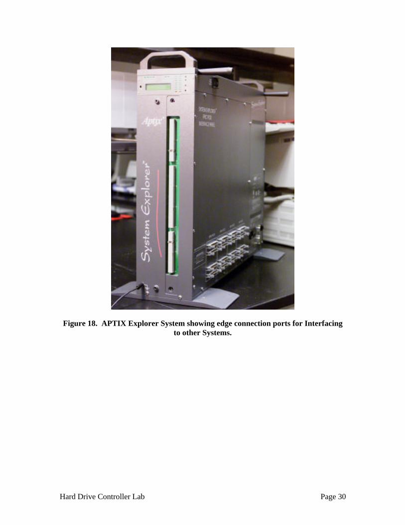
One problem is that one APTIX system normally would sell for $300,000 with softwaresupport. In addition, the LWL needs three copies of every item of equipment in order toservice the anticipated enrollment. However, APTIX as a small start-up had an unusualnumber of Rensselaer alumni and graduates of the CHD lab sequence. As a result threeAPTIX Explorer systems were found affordable on the ILI funds. The unexpected awardof the HP donation also made the purchase of three complete systems possible. The ILIaward had been shy of its intended target of $200,000 at $140,000 and the NSF

Hard Drive Controller Lab Page 29
recommended strategy had been to acquire only two deeply discounted APTIX systemsnot three. Because the HP donation had covered the needed oscilloscopes and logicanalyzers it became possible to acquire all three of the APTIX systems, and threecomplete systems of APTIX FPCB’s, ALPHAS, IBM INTELLISTATIONS,PAMETTES, HP 16,500 Logic Analyzers, HP Infinium Oscilloscopes, SUN U10SOLARIS workstations (for APTIX CAD tool suite), National Instruments PXI Boxes,and other HPIB or IEEE 488 compatible instruments (currently now includesprogrammable power supply and function generator).
Figure 18 shows the APTIX Field Programmable Circuit Board system packaged in aprotective box showing the large number of external connectors on the edge of the board.Figure 19 shows the numerous HP logic analyzer pod plugs (designed, as luck wouldhave it, specifically for the HP 16,500 logic analyzer, obtained on the HP grant)!
Figure 20 shows the back face opened to reveal the FPCB of the MP-4 showing the 4black FPIC chips along the center strip of the card, and the “free-hole” pin grid array forchip adaptor insertion above and below these four chips. Around the perimeter of thecard are various I/O transceiver chips providing isolation of the card from external ESDand driving capability for capacitive loading of external flexprint cables. Figures 21 and22 show various close-up views of the free-hole pin grid array and FPIC crossbar chipareas of the card, while Figures 23 and 24 seek to identify additional sections on the card.These figures also show substantial adaptor population showing the kinds of chipadaptors used. Some of these adaptors have more than one chip on them acting as a kindof multi chip module. Close-up photos of Figures 25 shows the adaptor obtained with thegrant holding a VERTEX V800 part, and the reverse side of the adaptor showing the pingrid array. Figure 26 shows a comparable part for an Altera FLEX 10,000 part.
Hard Drive Controller Lab Page 30
Figure 18. APTIX Explorer System showing edge connection ports for Interfacingto other Systems.

Hard Drive Controller Lab Page 31
Figure 19. Face of the APTIX MP-4 Explorer showing HP 16500 Logic AnalyzerPlugs.
Figure 20. Open Back Face of APTIX MP-4 FPCB showing the 4 FPIC crossbarswitches .

Hard Drive Controller Lab Page 32
Figure 21. Zoom in towards the FPCB “freehole” pin grid array just below theAPTIX FPIC.
Figure 22. Closer Zoom in on pin grid array and 4 APTIX FPIC crossbars.Automated wiring is provided by the FPIC’s between any pair of pins.

Hard Drive Controller Lab Page 33
Figure 23. Location of I/O Pin and I/O Isolation Drivers
Figure 24. Location of Low Skew clock and some of the bus drivers.

Hard Drive Controller Lab Page 34
Figure 25. Shows a typical standard APTIX adaptor for a Xilinx VERTEX V800part obtained in the APTIX grant. The right image shows the pin side of the
adaptor.
Figure 26. Alltera FLEX 10,000 series part on APTIX adaptor

Hard Drive Controller Lab Page 35
Figure 27. SUN based Software/CAD support flow provided by APTIX forheterogeneous mix of FPGA and dense VLSI integrated circuit components.
The software support for the APTIX board is outlined in Figure 27. A mixture of supportfor loading compiled code for microprocessors, IP cores in the form of ASIC circuits andFPGA configuration bits are downline loadable from a SUN based CAD tool suite.
Hard Drive Controller Lab Page 36
Progress on the Road to the “CHD Lab without Lights” Project.
A student taking the CHD fully remoted for distance learning would have to enter the labcompletely electronically. First the student would have to have any computer that cansupport NETSCAPE and host the Win98 operating system under which both Xilinx andand Altera CAD tools operate. It has been discovered that for students using a homeMAC instead of a PC that operation of both Xilinx and Altera CAD tools will operateusing the package Virtual PC offered by Connectix running Win98 on the MAC. Alsomany of the newer SUN workstation have a “sidekick” Pentium board at satisfactoryclock rate and will open a Win98 environment on that platform too. DEC alphas also canrun Win NT and there are varients for the tools on these machines also. It is hoped thatwhatever tools are developed a student owning or seeking to obtain access on any ofthese platforms operating with NETSCAPE would be able to enter the lab in this manner.
Using the CAD tools at home the student would create a solution for a prescribedproblem, such as “build a floppy disk controller for the PCI bus,” or “build a LANinterface to VME bus. These solutions could rely partially on the simulation capabilityprovided with the CAD tools. Students then would either compile the designs to createthe reconfiguration bit patterns for the FPGA’s or FPCB’s in the lab, or cross compile ona central SUN server [which both Xilinx and Altera support] to create bit patterns for thelarger parts. Xilinx 4028 and 4036 parts, for example, are not supported by the CADtools but the designs can be created for them anyway. Compilation for the larger chipshave to be accomplished by opening a Telnet connection to the SUN license machine andtime sharing the compiler.
Regardless of how the reconfiguration bit patterns are created they may be loaded on theDEC “study” machines which support the PCI, VME and SCSI bus protocols. TheseAlphas support under UNIX the tools needed to download to the DEC PCI Pamette orAnnapolis VME Wild-Force cards. After this the Telnet connection permits them to fireup a excitation program or “driver” to exercise their design from the Alpha. Various bitpatterns can be thrown at the design by editing the excitation files using simulated resultsor ad-hoc tests. The student then initiates the instrument remotely using the ubiquitousweb browser NETSCAPE and makes remote settings, collecting results from theinstrument in order to decide what to change in the design, unless, of course the designworks right the first time.
The entire configure/excitation/test sequence can take as little as a few minutes,permitting the student to then disconnect and surrender the station to another remote user.A scheduler operating on a DEC Alpha server then checks periodically to make sure thestudent is off the study machines named Alpha1, 2 and 3 respectively. Alpha0 is theDEC server. The DEC server also periodically checks to see if a student has locked uptheir respective alpha bus, and initiates a reset and reboot to that machine, taking intoaccount the time for rebooting, and scheduling new users once the machine is freshlyreconfigured for another student.

Hard Drive Controller Lab Page 37
This issue of how one initiates contact with the instruments is key to how the operationwill proceed in the lab. HP-V is an excellent way to view an instrument over thenetwork, but apparently some one in the lab needs to create access to the instrument atthe instrument end. This is not consistent with the goals of the lab without lights inwhich the student can open measurement windows. While these tools present excellentrenditions of the scope and logic analyzer over ordinary network connections, theyhowever do make the instrument vulnerable to network hacks. Rebooting of theinstrument on Win95 or Win98 is a bit awkward, and virus attack over the network couldleave the instrument in an unusable state. Consequently the NI boxes are used toestablish a kind of fire wall to the instruments, talking to them only with HPIB (or thenow adopted IEEE488 standard). Viruses cannot attack the Win95/98 instrument coresin this arrangement, although they can attack the NI box. However this arrangement isconsidered preferable since only one box then is vulnerable, not every instrument. TheDEC Alpha server also has to check the health of this NI box periodically to see if it isawake.

Hard Drive Controller Lab Page 38
Development of LWL labs – Status and Retrospective
Development of new Labs takes many years. A combination of talented TeachingAssistants and Masters Degree candidates are required to conceptualize the labs anddevelop lab write-up documents and web-based aids. In this case the idea for the firstLWL lab came from the students taking the course themselves. As a project for theadvanced course an option was provided for students to develop a new lab. One groupelected to create a on line IDE disk controller for PCI bus. The result has been attachedas Appendix A and was developed in the spring of 2000. This year (2001) is the firstyear the lab has been deployed and seems to be successful, though evaluation of the effortwill unfortunately require several more weeks beyond the point where this report must besubmitted. Hence quantitative measurements of the pedagogical aspects of the projectwill take more time.
Figure 28 shows the IDE drive with the HP Infinium oscilloscope capturing signals fromthe disk drive interface, while the computer display at the right shows a Logic analyzerscreen dump as can be observed remotely
Figure 28. IDE Drive with flex print cable going to the ALPHA
The oscilloscope used in the IDE lab can be accessed using NETSCAPE on any PCincluding laptop units provided a high speed internet connection is available. This

Hard Drive Controller Lab Page 39
interface has been tested for responsiveness at remote locations including Austin, Texas,Santa Clara, California, and Atlanta Georgia.
Figure 29. Remote HP Infinium CGI interface played through the NationalInstruments “fire wall” interface to the network using NETSCAPE.
Access to the lab is by one of the following two web sites.
http://pxi2.cie.rpi.edu
http://alpha2.cie.rpi.edu

Hard Drive Controller Lab Page 40
Figure 30. Internet Explorer view of the HP 16,500 through the National Instgruments“fire-wall”.

Hard Drive Controller Lab Page 41
The SUN Grant
The APTIX systems depend on SUN workstations to support their CAD tools and so oneof the final chapter in the ILI report must take recognition of one of the other companiongrants from SUN which has placed three SUN U10 workstations in the LWL along withabout 55 other U10 stations located throughout the ECSE department. Each station has256MB of main memory, 440 MHz processor, 9 Gb of disk, a 300MHz 128 MB Pentiumsidekick coprocessor card and 21 inch color monitor. The impact of the SUN grant hasbeen perhaps only conservatively listed at $15K for the three stations actually in thelaboratory. However, because all of the stations can be used to enter the labelectronically by telnet connections at high bit rates of 100 Mb/s the actual size of thegrant is much larger.
Figure 31 and 32 show various views of these stations in two of the key publicworkstation areas in the ECSE department.
Figure 31 Public SUN U10 Workstation area in Johnson Engineering Center.

Hard Drive Controller Lab Page 42
Figure 31. CII 6118 Workstation Room adjacent to the LWL with 12 SUN U10’s.
Figure 32. 17 SUN U10’s located in the JEC SUN studio.

Hard Drive Controller Lab Page 43
Pedagogical Issues in the “CHD Lab without Lights” Project
Some issues have come up with the totally remote “CHA Lab without Lights” approachone of which is how to prevent cheating. It could be possible for a student to simplydump the bits from a design from another student into the FPGA board and claim thesolution was theirs. For this purpose a “cookie” has to be created for each student thattells us their design meets a uniqueness criterion. Currently this “cookie” would have tobe incorporated into a design as a kind of piece of hardware that the excitation programcan check to see that at least the student has the key to the corresponding lock in theirhardware solution.
Taking a Peek at the Future
During the period of development of the “CHD Lab without Lights” project the followingweb site is being maintained as a sampler of things to come. Eventually a much morepowerful gateway will be developed into the lab, checking passwords, and preventingmischief. For the moment the sampler is at:
http://pxi2.cie.rpi.edu
This site is not always active. It is down when the conventional lab needs the instrumentand when the DA is working on new lab material. Requsts to activate the site can bedirected towards the Principle Investigator at
The revised course attracted an increased initial enrollment of 80 vs. 50 students in theprevious year, based only on the presence of the new equipment in the lab. It is expectedthat this number will grow to 100 as new labs get developed, attracting new students fromEE, CSE and CS majors. Computer hardware design represents both a strong area ofresearch at Rensselaer, meshing well with the activities of the SRC-funded CAIST, andan outstanding area of potential employment for students at BS, MS/MEng and PhDlevels. Consequently, both research and teaching benefited from this investment. Thisreport will primarily focus on the benefits to teaching.

Hard Drive Controller Lab Page 44
Appendix A
Rensselaer Polytechnic InstituteAdvanced Computer Hardware Design – ECSE-6700
Design of an IDE Hard Drive Controller
OBJECTIVE
To complete a design of an IDE hard drive controller interface on an FPGA in the ‘LabWithout Lights’ via the PAMETTE module on the DEC Alpha Server. Due to thecomplexity of the many signals on the PAMETTE card needed to interface with theoutside world, part of the interface has already been defined and will be supplied inVHDL files. The entire lab was first composed in VHDL entirely, although it is not arequirement for this lab. Schematic capture should work just as well.
INTRODUCTION AND OVERVIEW
The main part of this system is an IDE controller, which is located on the hard disk driveitself. In order to communicate with the disk drive, an interface must be designed thatcommunicates between the host computer and the IDE disk drive controller. Thisinterface is to be designed on an FPGA located on the PAMETTE card. This PAMETTEcard plugs into a PCI slot of the DEC Alpha server and is programmed remotely. Userscan communicate with the PAMETTE card through a C program, which contains thenecessary PAMETTE libraries.
DESCRIPTION OF PAMETTE CARD
The PAMETTE module, also known as the PCI Development Platform module, iscomposed of 5 FPGAs (Field Programmable Gate Arrays). One of these FPGAs isresponsible for controlling the PCI (Peripheral Component Interconnect) bus while theother four are user configurable. These components can be reprogrammed infinitely,which makes them very useful for a lab such as this in which several editions of thedesign may be needed. A block diagram of the PAMETTE card is shown below inFigure 2.1.
RPI

Hard Drive Controller Lab Page 45
Figure 0-1. PCI Development Platform Module Overview
Clocking Circuitry
The clocking circuitry on the PAMETTE board is composed of two independent clockingsystems, the user clock and the system clock. Both of these clocks are distributed to allof the FPGAs. The system clock is an in-phase copy of the PCI clock at the PCIfrequency or double the PCI frequency. The user clock is a programmable frequencygenerator, with a frequency range of 400 kHz to 100 MHz with a resolution of about0.5%. It has no defined phase relation to the PCI clock.
2.1.2. Software
In order to complete this lab, it will be necessary to use two computer systems in theCHD lab.
The PAMETTE board used in this lab has been installed on a DEC Alpha server runningDigital UNIX. The Alpha server already has the software you will need for this lab.While you will not be required to write the testing and interface software for this lab, thesource code is available in the “idesoftware” directory. More detail about using thesoftware is in section 3.5.
The necessary Xilinx tools can be found on the Intel PCs in the lab. Xilinx Foundation3.1i software is also available in Troy 2012. Instructions for compiling a design are insection 6.
PAMETTE Reference material

Hard Drive Controller Lab Page 46
For a detailed description of the PAMETTE card, refer to the DIGITAL PCI DevelopmentPlatform Re-configurable Hardware Device for the PCI Bus User’s Guide, April 1998.The user’s guide is available in the CHD lab.
Electronic copies are available in the document directories in CHD PCs and Alpha's inPDF format
Description of VHDL
VHSIC Hardware Description Language (VHDL) is a language for describing digitalelectronic systems. It is basically a standard language for describing the structure andfunction of integrated circuits. It has many advantages that aid in the digital designprocess. First, it allows the detailed structure of a design to be synthesized from anabstract specification. This is important because most modern designs are extremelycomplex and it would be very difficult to use schematics to design such complicatedsystems. It also allows a designer to simulate a design before implementing it, whichsaves vast amounts of time and money (although simulation can also be performed usingschematics).
VHDL was used for the design of the IDE controller interface, as well as the othervarious interfacing components that had to be implemented to make this project work.However, it is not required for this project. The design can be performed just as wellusing circuit schematics. Bear in mind that in today’s hardware design industry, mostcompanies use hardware description languages (VHDL, Verilog) because of thecomplexity of the designs and the advantages mentioned above. Therefore, it isextremely advantageous for students to have some experience in VHDL when searchingfor employment.
There are many references that can be used to learn VHDL. Everything needed toimplement the design for this lab can be found in the required textbook for ECSE-4770Computer Hardware Design, titled ‘Rapid Prototyping of Digital Systems’ by Hamblenand Furman. Specifically, chapter 6 titled ‘Using VHDL for Synthesis of DigitalHardware.’
Assignment
Goals
This lab has several objectives. First, it will familiarize the student with programming anFPGA remotely via the DEC Alpha server. Also, it teaches the student how an IDE harddisk controller works and how to design an interface to it. In addition, it also gives thestudent more experience with state machine design and the opportunity to gainexperience in VHDL.
Hard Drive Controller Lab Page 47
Intelligent Drive Electronics (IDE) Hard Drive
An IDE hard drive is a storage element that contains built-in controlling hardware on thedrive. The controller accepts external signals and performs the required tasks of reading,writing and decoding data. Hence the drive is ‘intelligent’ as the name refers.
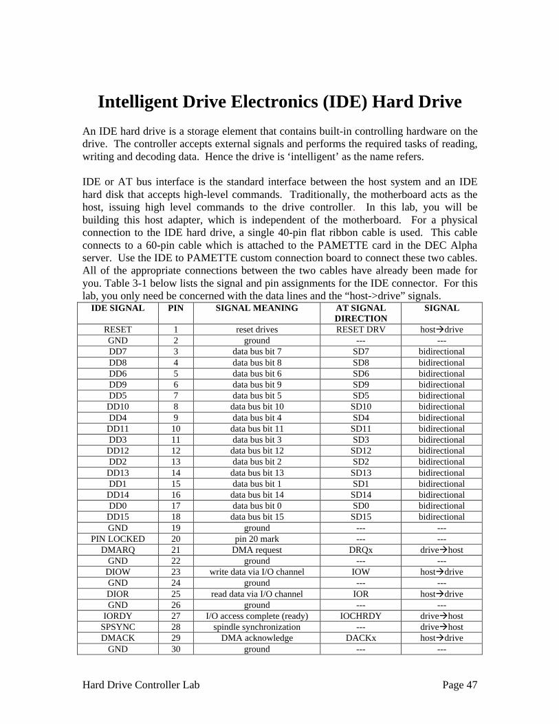
IDE or AT bus interface is the standard interface between the host system and an IDEhard disk that accepts high-level commands. Traditionally, the motherboard acts as thehost, issuing high level commands to the drive controller. In this lab, you will bebuilding this host adapter, which is independent of the motherboard. For a physicalconnection to the IDE hard drive, a single 40-pin flat ribbon cable is used. This cableconnects to a 60-pin cable which is attached to the PAMETTE card in the DEC Alphaserver. Use the IDE to PAMETTE custom connection board to connect these two cables.All of the appropriate connections between the two cables have already been made foryou. Table 3-1 below lists the signal and pin assignments for the IDE connector. For thislab, you only need be concerned with the data lines and the “host->drive” signals.
IDE SIGNAL PIN SIGNAL MEANING AT SIGNALDIRECTION
SIGNAL
RESET 1 reset drives RESET DRV hostàdriveGND 2 ground --- ---DD7 3 data bus bit 7 SD7 bidirectionalDD8 4 data bus bit 8 SD8 bidirectionalDD6 5 data bus bit 6 SD6 bidirectionalDD9 6 data bus bit 9 SD9 bidirectionalDD5 7 data bus bit 5 SD5 bidirectionalDD10 8 data bus bit 10 SD10 bidirectionalDD4 9 data bus bit 4 SD4 bidirectionalDD11 10 data bus bit 11 SD11 bidirectionalDD3 11 data bus bit 3 SD3 bidirectionalDD12 12 data bus bit 12 SD12 bidirectionalDD2 13 data bus bit 2 SD2 bidirectionalDD13 14 data bus bit 13 SD13 bidirectionalDD1 15 data bus bit 1 SD1 bidirectionalDD14 16 data bus bit 14 SD14 bidirectionalDD0 17 data bus bit 0 SD0 bidirectionalDD15 18 data bus bit 15 SD15 bidirectionalGND 19 ground --- ---
PIN LOCKED 20 pin 20 mark --- ---DMARQ 21 DMA request DRQx driveàhost
GND 22 ground --- ---DIOW 23 write data via I/O channel IOW hostàdriveGND 24 ground --- ---DIOR 25 read data via I/O channel IOR hostàdriveGND 26 ground --- ---
IORDY 27 I/O access complete (ready) IOCHRDY driveàhostSPSYNC 28 spindle synchronization --- driveàhostDMACK 29 DMA acknowledge DACKx hostàdrive
GND 30 ground --- ---

Hard Drive Controller Lab Page 48
INTRQ 31 interrupt request IRQx driveàhostIOCS16 32 16 bit transfer via I/O channel I/OCS16 driveàhost
DA1 33 address bus 1 SA1 hostàdrivePDIAG 34 passed diagnostic from slave --- driveàhost
DA0 35 address bus 0 SA0 hostàdriveDA2 36 address bus 2 SA2 hostàdrive
CS1Fx 37 chip select for base addr. 1f0h --- hostàdriveCS3Fx 38 chip select for base addr. 3f0h --- hostàdriveDASP 39 drive active/slave present --- driveàhostGND 40 ground --- ---
Table 0-1. IDE Interface Cable Layout
A note about noiseIn order to reduce noise, you may have to insert capacitors on the IDE ribbon cableconnector. There should be three connectors along the ribbon cable, and you can insertcapacitors into the center connector in order to smooth out noise on the IDE bus. Thefollowing capacitor values work well:
Capacitor Value From IDE Pin To IDE Pin10.6nF 23 242.4nF 25 262.4nf 37 40Remember that IDE Pin 1 lies next to the red line on the IDE ribbon cable on the sameside as the black notch. Pin 2 is below it, and so on.
System Design
Top-Level Design of System
While the PAMETTE board has four FPGAs (also referred to as LCAs in the PAMETTEdocumentation) that can hold custom designs, this lab will only use two of them. LCA1will hold all of the logic needed to implement the IDE controller, and LCA3 will route

Hard Drive Controller Lab Page 49
the signals from the output of the IDE controller to the ribbon cable. The design of LCA3has already been compiled for you.
LCA1 Components (Larger figure is attached on the last page)
LCA1 connects the EBUS, which is a bus on the PAMETTE card where data from thePCI bus is available, with LCA3. Your group will be responsible for creating theIDE_CONTROLLER section of the design, which communicates with the EBUS thoughtwo registers, as described in the communication protocol section.
Host to IDE Communication Protocol
For this lab, you will be designing the ide_interface component as pictured in the systemdiagram. The software on the host PC communicates over the PCI bus through two 32-bitregisters on the PAMETTE card. The PC can write data into the register instr_reg, andcan read from the output register result_reg. Your state machine will read from instr_reg,perform a command based on the contents, and then return data back in result_reg.
Additionally, there are three control signals that help manage these registers. The firstcontrol signal, the available_instr flag, is asserted when the PC writes data intoinstr_reg,.
Drive Controller

Hard Drive Controller Lab Page 50
Your state machine will signal that it is reading from the instruction register by raisingyet another signal, read_instr. This action must lower the available_instr flag. You maycontinue to read from the register until you lower the read_instr flag, after which theinstr_reg inputs to your state machine are undefined.
Use the write_instr output flag to trigger a write to the result_reg register. Data is writtenon the rising edge of this signal.
The input register, instr_reg, is formatted into three parts: +----------------+----------------+--------------------------------+ | instr_command | instr_address | instr_data | +----------------+----------------+--------------------------------+ 31 24 23 16 15 0
The instr_command field of instr_reg should be parsed to an 8 bit register appropriatelynamed instr_command in the VHDL state machine you will be designing. While it isdefined as an 8-bit register (for future expansion to include more commands), only thelower two bits will need to be decoded since there are currently only three commands:
0x00 No-opPerform no action, but return a result word as described below.
0x02 Write registerWrite the value contained in instr_data to the register on the drive ataddress instr_address.
0x03 Read registerRead the register on the drive at address instr_address, and return thevalue in the result_data field of the result word.
The instr_address field specifies the address of the register for read and write commands.The hard drive has 16 registers, 8 of which are enabled with the ide_cs_1f0_n signal, andthe other 8 of which are enabled with the ide_cs_3f0_n signal. Since the PC software onlyuses registers in the 1f0 range, the address field will only be defined for the bottom threebits; the rest can be ignored. These bits should be sent to the drive as a 3 bit registernamed ide_address in order to specify operations on the IDE bus. The instr_data field isa 16-bit wide field, which specifies the data to be written to the drive whenever a writecommand (0x02) is issued. It should contain all zeros for all other commands. This datashould be directly sent to a 16-bit buffer defined in your state machine named ide_dataduring the data phase of an IDE write. It should be noted that the drive will ignore theupper 8 bits of the ide_data field during an 8-bit transfer.
After a valid instruction has executed, the ide_controller state machine is expected toreturn a result code to the result_reg register. This register is formatted with thefollowing fields:
+----------------+----------------+--------------------------------+ | result_command | result_status | result_data | +----------------+----------------+--------------------------------+ 31 24 23 16 15 0

Hard Drive Controller Lab Page 51
The result_command field should contain the same value that was passed in theinstr_command field. This field exists so that the PC software can match up results wordswith the command words that were sent previously.
The result_status field exists for error reporting. For extra credit, your state machine canreturn a non-zero code in this field if it detects a problem with the IDE bus. The PCsoftware will recognize a non-zero result code and output an error message to the screen.Make sure to document your error status codes if you choose to use them. If your designdoes not detect errors, always return zero in this field.
The result_data field is where the data will be returned to the PC for a read command(0x03). For all other commands, the interface software will ignore this field, so its valueis not important for any other commands. The PC software will also ignore the uppereight bits of this register during an 8-bit register read, so your design may always take theentire 16-bits of the ide_data bus and return them in this register without regard to thetype of transfer.
Using the IDE Controller test programs
There are three test programs you may use to test your group’s design. Each expects toload an ide.pam file from the current directory, so make sure you start these programsfrom your group’s directory.
The cmdtest program allows you to send your state machine some instruction words andsee the returning result word. Since none of the other test programs will work if you donot see the correct result words, this should be the first test of a new design.
When you see the “>” prompt, type in a 32-bit integer in hex to be sent to theIDE_CONTROLLER state machine. This value will be sent as the command word, andthe result word the state machine outputs will be displayed. Enter “Q” to quit.
Example instructions could be:> 02031234 Send a write instruction, address 3, data 1234.> 03070000 Send a read instruction, address 7.
The drivetest program allows you to see the contents of all of the hard drive’s controlregisters. It also allows writes to registers. When the program starts, it will reset the statemachine, which should send a reset to the drive. When the reset is complete, the drivetestprogram gets the values of all eight control registers by using the “read register”command, 0x03.
The drivetest program then gives the user a prompt. At this prompt, enter the number ofa register and a value to write and the drivetest program will send this to the drive usingthe “write register” command, 0x02. If you enter no data and just press the enter key, thedisplay will be refreshed. Type “Q” to quit.

Hard Drive Controller Lab Page 52
The ide2 program is the largest test program. It allows reading to and writing fromsectors on the hard drive using your design. If the other two test programs have worked,you should be able to use this program to send data to and retrieve data from the drivefollowing the on-screen prompts. This program will return back the information stored inan entire sector of hard drive.
VHDL Reference
Writing a state machine in VHDL
(Note: The majority of this section can be found in chapter 6 of Rapid Prototyping ofDigital Systems, 2000 edition)
If you choose to implement your state machine in VHDL, it is important to remember afew concepts that will assist you in your design and simulation phase. Although VHDLlooks like any other programming language, it does not act the same way. Rememberthat VHDL is used to implement hardware. Logic gates and I/O pins are often connectedin parallel, and can perform many operations simultaneously. When programming a statemachine in VHDL, keep in mind that your code will not be executed line by line, orsequentially. All instructions in each state of your state machine will be executedsimultaneously, so plan accordingly.
Begin by declaring all of the states in your state machine. After defining all of the inputand output ports, create a new architecture for your state machine and define variables forall of your states as state_types. This is shown in the example below:
ARCHITECTURE state_machine_name OF entity_name IS
TYPE STATE_TYPE IS (
STATE_ONE, --name of first stateSTATE_TWO, --name of second stateEtc…);
Now you can define internal signals that only your state machine will use. In thiscase, a signal to indicate the current state that the state machine will be in, and an 8-bitbuffer are defined:
SIGNAL state : STATE_TYPE;
SIGNAL buffer : STD_LOGIC_VECTOR(7 downto 0);
Finally we can begin the design phase of our VHDL state machine! Your statemachine will most likely be driven by external signals coming into the FPGA chip. Letus assume that in the I/O port section, the following incoming signals exist:

Hard Drive Controller Lab Page 53
clk : IN STD_LOGIC; --the clock signalreset : IN STD_LOGIC; --resets the whole state machineincoming_signal : IN STD_LOGIC; --controlled by some external event
You should begin by defining what should happen when the state machine is firstturned on. Usually this involves resetting the state machine. Thus, begin by initializingall signals, and setting the next state to STATE_ONE:
BEGINPROCESS (clk)BEGIN
IF reset = '1' THENstate <= STATE_ONE;buffer <= “00000000”;incoming_signal <= ‘0’;
Bear in mind that the three commands in the conditional statement above will beexecuted simultaneously whenever the reset signal is raised, regardless of which state thestate machine is in. When all three commands are complete, the state machine will be instate one. The next few lines of code instruct the hardware to check the state machineinput signals on every rising edge of the clock, and perform operations depending onwhat the current state is.
ELSIF clk'EVENT AND clk = '1' THENCASE state IS
WHEN STATE_ONE =>IF incoming_signal = '1' THEN
state <= STATE_two;ELSE
state <= STATE_ONE;buffer <= “00000000”
END IF;
WHEN STATE_TWO =>buffer <= “11111111”;state <= STATE_ONE;
END CASE;END IF;
END PROCESS;
END state_machine_name;
So if you haven’t figured it out by now, this extremely simple state machine fills bufferwith all high signals whenever the incoming signal is high. STATE_ONE is the waitstate that the state machine will reside in safely when no external activity is occurring.Of course, your state machine will be a bit more complex and might incorporate casestatements within the main case statements in order to recognize incoming commandsand act accordingly.

Hard Drive Controller Lab Page 54
Signal naming
For your state machine, you must use the following signal names in order tocommunicate with the other modules on the PAMETTE board. Use the following linesas the beginning of your state machine VHDL code:
LIBRARY IEEE;USE IEEE.std_logic_1164.all;
ENTITY WFIdeInterface ISPORT(
---------- CONNECTIONS FROM PAMETTE CARD --------------clk reset fifo inp, fifo outp, fifo i/o cntlclk : IN STD_LOGIC;
reset : IN STD_LOGIC;instr_command : IN STD_LOGIC_VECTOR(7 downto 0);instr_address : IN STD_LOGIC_VECTOR(7 downto 0);instr_data : IN STD_LOGIC_VECTOR(15 downto
0);result_command : OUT STD_LOGIC_VECTOR(7 downto 0);result_status : OUT STD_LOGIC_VECTOR(7 downto 0);result_data : OUT STD_LOGIC_VECTOR(15 downto
0);available_instr : IN STD_LOGIC;read_instr : OUT STD_LOGIC;write_result : OUT STD_LOGIC;
----------- CONNECTIONS TO IDE INTERFACE --------------- IDE Signal nameide_reset_n : OUT STD_LOGIC; -- RESETide_data : INOUT STD_LOGIC_VECTOR(15 downto 0); -- DD[15:0]ide_data_write_n : OUT STD_LOGIC; -- DIOWide_data_read_n : OUT STD_LOGIC; -- DIORide_address : OUT STD_LOGIC_VECTOR(2 downto 0); -- DA[2:0]ide_cs_1f0_n : OUT STD_LOGIC; -- CS1Fxide_cs_3f0_n : OUT STD_LOGIC; -- CS3Fxide_ready : IN STD_LOGIC; -- IORDYide_int_request : IN STD_LOGIC; -- INTRQide_16_bit_n : IN STD_LOGIC; -- IOCS16ide_dasp_n : IN STD_LOGIC -- DASP
);END WFIdeInterface;
Reference Section
PAMETTE Information
RPI CHD Lab - DEC PAMETTE Information
ftp://[email protected]/docs/overview.pdf

Hard Drive Controller Lab Page 55
PCI PAMETTE V1
http://research.compaq.com/SRC/pamette/
PCI PAMETTE documentation , schematics , and software
http://research.compaq.com/SRC/pamette/Download.html
PAMETTE to IDE interface board
http://www.technobox.com/pic1518.htmhttp://www.technobox.com/cat1518.pdf
Hard Drive References
0791M AT Attachment Interface for Disk Drives (ATA-1)
ftp://ftp.t13.org/project/d0791r4c.pdfORftp://[email protected]/docs/IDE_SPEC.pdf
VHDL References
Xilinx Online Documentation
http://toolbox.xilinx.com/docsan/3_1i/
The Hamburg VHDL Archive
http://tech-www.informatik.uni-hamburg.de/vhdl/
CHD Lab Remote Access
Remote access to the logic analyzer is available on one setup presently. The logicanalyzer is controlled by National Instruments PXI box. This PXI box is a GPIBcontrolling PC. Web access is available to these instruments. If required obtain yourusername and password from your TA.
http://pxi2.cie.rpi.edu
A Tutorial on Synthesizing and Implementing your State Machine design

Hard Drive Controller Lab Page 56
Introduction
After you complete simulating your state machine design in Xilinx (via VHDL orschematics), the next step is to synthesize and implement the design.
Check the syntax of all project code
1. Synthesis -> Force Analysis of all Sources2. Look for green check marks next to every project file
Synthesize code1. Click on the Synthesis button, the Synthesis/Implementation settings window shouldappear2. Set the Top Level field to pamtl_lca33. In the Target Device box, set the Family field to "XC4000EX"4. Set the Device field to 4028EXHQ2085. The Speed field should be set to "ex-2"
It should look a little something like this...
6. Click on the "SET" button, the settings window should appear.7. Change the Effort Level to "High"
You might see something along these lines...

Hard Drive Controller Lab Page 57
8. Click OK, and then click the Run button on the Synthesis/Implementation settingswindow.9. The program will then run through the Synthesizing process. Hopefully you will getno errors.
Implementation process
1. With your VHDL code now synthesized, it is time to implement it into a .bit file forthe Xilinx chip. Click on the Implementation button in the right windowpane of theProject Manager. Our friend the Synthesis/Implementation settings window will pay usanother visit.
2. Click on the SET button in the Physical Implementation settings box. A settingswindow will appear.

Hard Drive Controller Lab Page 58
3. Change the "Use Constraints file from" field to "Custom". A ‘Custom’ window willnow appear.4. Enter the Constraints File as "pamlca3.ucf" and click OK.
5. Click on the Options button. An Options window will appear.6. Click on the Edit Options button across from the Configuration pull down menu7. The Configuration tab of your XC4000 Configuration Options window, should looklike this:

Hard Drive Controller Lab Page 59
(All you should need to change are setting the I/O Threshold levels to TTL)
8. Click OK in each window until you get back to the Synthesis/Implementation window.At that point, click on Run, and watch the implementation magic!
9. A Flow Engine window will appear, and several programs will be called which checkyour design and create the necessary bit files. You should see this window when theimplementation process is done.
10. Click OK, and you are ready to begin testing your design! The final bit file is placedin the root directory of your project folder with a ".bit" extension.

Hard Drive Controller Lab Page 60
Copying files to the Alpha Server
Before you send your first design, you will need to set up a directory on the Alpha to holdyour group’s files. Use the telnet program to connect to alpha2.cie.rpi.edu. Choose aname for your group’s directory, and type “mkdir <your directory>”. Copy thefiles from the “studentdesign” directory to your directory using the command “cpstudentdesign/* <your directory>”.
Every time you compile a design using Xilinx Foundation 2.1i, you will need to move the.bit file to the Alpha so that it can be downloaded to the card. The easiest solution is touse the Windows FTP client. Select “Run...” from the Windows Start Menu, and type“ftp alpha2.cie.rpi.edu” in the box.
For those unfamiliar with FTP, a sample session is provided.
Connected to alpha2.cie.rpi.edu.
220 alpha2.cie.rpi.edu FTP server (Digital UNIX Version5.60) ready.User (alpha2.cie.rpi.edu:(none)): chduser331 Password required for chduser.Password: <your password>230 User chduser logged in.ftp> cd <your directory>250 CWD command successful.ftp> binary200 Type set to I.ftp> put <your design.bit>200 PORT command successful.150 Opening BINARY mode data connection for yourdesign.bit(24.161.0.21,62779).226 Transfer complete.ftp: 40180 bytes sent in 0.00Seconds 40180000.00Kbytes/sec.
ftp> quit221 Goodbye.
Once the design has been transferred, switch back to the telnet window, change to yourdesign’s directory using “cd <your directory>”, and run “make”. This should runthe mergebit program to combine your design for LCA 1 with the designs for the otherLCAs which have been provided for you. The warnings that mergebit cannot find thesymbol file for your design are not a problem.
Once mergebit has produced the ide.pam file in your project’s directory, you may run thetest programs as described in section 3.5.
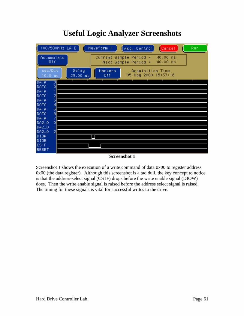
Hard Drive Controller Lab Page 61
Useful Logic Analyzer Screenshots
Screenshot 1
Screenshot 1 shows the execution of a write command of data 0x00 to register address0x00 (the data register). Although this screenshot is a tad dull, the key concept to noticeis that the address-select signal (CS1F) drops before the write enable signal (DIOW)does. Then the write enable signal is raised before the address select signal is raised.The timing for these signals is vital for successful writes to the drive.

Hard Drive Controller Lab Page 62
Screenshot 2
Screenshot 2 is a bit more interesting. It shows the timing involved for writing 0x55 toregister address 1 (the error register, which by the way is read-only).
Screenshot 3

Hard Drive Controller Lab Page 63
Screenshot 3 illustrates a read from register 7 (the command register) with 0x50 on thedata bus. The corresponding op-code for this command would be “03070050” accordingto the IDE communication protocol defined in section 3.3. The interface program shouldthen return the contents of the data in the result register. Since this is a read operation,the data in the instr_data field (DATA 0 through DATA 7 in screenshot 3) will beignored by the drive. Note that the read enable signal (DIOR) is raised at the same timeas the address select signal (CS1F). This timing is acceptable for a read operation.
Source Code for Interface Program
IDE Constants header File/***************************************************************************** * ideconstants.h *======================================================================== * Defines for the ide interface * * Advanced Computer Hardware Design * Adam Belsky, Chris Hahn, Bob Juras, Jeff Opalka * * 02 MAR 2000 - initial revision
****************************************************************************/
#ifndef _IDECONSTANTS_H_
#define OK 0#define FAIL 1#define SECTOR_SIZE 512
#define REG_DATA 0x0#define REG_ERROR 0x1#define REG_PRECOMP 0x1#define REG_NUMSECT 0x2#define REG_SECTOR 0x3#define REG_CYLLSB 0x4#define REG_CYLMSB 0x5#define REG_DRIVEHEAD 0x6#define REG_STATUS 0x7#define REG_COMMAND 0x7#define REG_ASR 0xe#define REG_DOR 0xe#define REG_DADDR 0xf
/* constants for the error register - REG_ERROR */#define ERR_NDM 0x80#define ERR_NTO 0x40#define ERR_ABT 0x20#define ERR_NID 0x08

Hard Drive Controller Lab Page 64
#define ERR_UNC 0x02#define ERR_BBK 0x01
/* constants for the status register - REG_STATUS */#define STATUS_BSY 0x80#define STATUS_RDY 0x40#define STATUS_WFT 0x20#define STATUS_SKC 0x10#define STATUS_DRQ 0x08#define STATUS_CORR 0x04#define STATUS_IDX 0x02#define STATUS_ERR 0x01
/* constants for our design */#define COMMAND_NOOP 0x00#define COMMAND_CKBUSY 0x01#define COMMAND_WRITEREG 0x02#define COMMAND_READREG 0x03#define COMMAND_RESET 0x04
/* timeout for waiting for the busy bit -- 16 = 160 microsecs */#define DRIVE_TIMEOUT 1000
#endif // _IDECONSTANTS_H_
IDE Utilities Header File/***************************************************************************** * ideutils.h *======================================================================== * Low-level communications routines for the Pamette card. * * Advanced Computer Hardware Design * Adam Belsky, Chris Hahn, Bob Juras, Jeff Opalka * * 31 MAR 2000 - initial revision
****************************************************************************/
#ifndef __IDEUTILS_H__#define __IDEUTILS_H__
/* high-level IDE communcations functions */int initializeIDE();int resetDrive();int formatTrack(int cyl, int head);int readSector(int cyl, int head, int sect, unsigned char *data);int writeSector(int cyl, int head, int sect, unsigned char *data);int printInfo();

Hard Drive Controller Lab Page 65
int closeIDE();int checkError();char* getLastError();
/* low-level FPGA-card communications functions */
int writeRegister(int addr, unsigned short data);int readRegister(int addr, unsigned short *data);
int initializeCard();int closeCard();int resetCard();int sendCommand(unsigned char command, unsigned char address, unsignedshort indata, unsigned short *outdata);
#endif /* __IDEUTILS_H__ */
IDE Utilities Source Code/***************************************************************************** * ideutils.cpp *======================================================================== * Low-level communicatrions routines for the Pamette card. * * Advanced Computer Hardware Design * Adam Belsky, Chris Hahn, Bob Juras, Jeff Opalka * * 27 FEB 2000 - initial revision * 30 APR 2000 - ported to digial unix/pamette
****************************************************************************/
#include <stdio.h>#include <stdlib.h>#include <string.h>#include <unistd.h>#include <PamRT.h>#include <PamFriend.h>
#include "ideutils.h"#include "ideconstants.h"
// dec's header files don't seem to define thisextern "C" { void usleep(unsigned int);}
/*****************************************************************************

Hard Drive Controller Lab Page 66
* The first section of this file is a hardware-independentimplementation * of the ide protocol. It issues requests to the actual hardwarethough * the hardware-dependent functions, which are in the second half ofthis file.
*****************************************************************************/
/* error handling routines */char lasterror[100];
char* getLastError(){ return lasterror;}
/* this just forwards the init call to the hardware-dependent initfunction */int initializeIDE(){ return initializeCard();}
int resetDrive(){
return resetCard();}
int checkError(){
int retval;unsigned short status, err;
retval = readRegister(REG_STATUS, &status); if (retval != OK) return retval;
if (status & STATUS_ERR) {retval = readRegister(REG_ERROR, &err);if (retval != OK) return retval;sprintf(lasterror, "Drive has error bit set. Error
register contains 0x%02x.", err & 0xff);return FAIL;
}
return OK;}
/* wait until the drive is not busy */int waitBusy() { int count = 0; int retval;

Hard Drive Controller Lab Page 67
unsigned short status;
usleep(10);
/* wait for busy */ retval = readRegister(REG_STATUS, &status); if (retval != OK) return retval;
while (((status & STATUS_BSY) || ((status & STATUS_DRQ) !=STATUS_DRQ)) && (count < DRIVE_TIMEOUT)) { usleep(1000); /* wait 1 ms for drive to not be busy */ retval = readRegister(REG_STATUS, &status); if (retval != OK) return retval; count++; }
/* if we timed out */ if (count >= DRIVE_TIMEOUT) { sprintf(lasterror, "timed out waiting for drive to lower busyflag."); return FAIL; } else { return OK; }}
/* wait until the drive says it's ready */int waitReady() { int count = 0; int retval; unsigned short status;
usleep(10);
/* wait for ready */ retval = readRegister(REG_STATUS, &status); if (retval != OK) return retval;
while (((status & 0x0040) != 0x40) && (count < DRIVE_TIMEOUT)) { usleep(1000); retval = readRegister(REG_STATUS, &status); if (retval != OK) return retval; count++; }
/* if we timed out */ if (count >= DRIVE_TIMEOUT) { sprintf(lasterror, "timed out waiting for drive ready."); return FAIL; } else { return OK; }}
/* issue the right register accesses to format a track */

Hard Drive Controller Lab Page 68
int formatTrack(int cyl, int head){ int retval = 0;
/* send the format track parameter */ retval = writeRegister(REG_CYLLSB, (cyl & 0x00ff) ); if (retval != OK) return retval; retval = writeRegister(REG_CYLMSB, (cyl & 0xff00) >> 8); if (retval != OK) return retval; retval = writeRegister(REG_DRIVEHEAD, 0xa0 | (head & 0x0f) ); if (retval != OK) return retval; retval = writeRegister(REG_COMMAND, 0x30); //write sector, no ecc, noretry if (retval != OK) return retval;
if (waitBusy() != OK) { return FAIL; }
return OK;}
/* issue the right register accesses to read a sector */int readSector(int cyl, int head, int sect, unsigned char *data){ int retval = 0; unsigned short tempr;
retval = writeRegister(REG_NUMSECT, 1); if (retval != OK) return retval; retval = writeRegister(REG_SECTOR, (sect & 0xff) ); if (retval != OK) return retval; retval = writeRegister(REG_CYLLSB, (cyl & 0x00ff) ); if (retval != OK) return retval; retval = writeRegister(REG_CYLMSB, (cyl & 0xff00) >> 8); if (retval != OK) return retval; retval = writeRegister(REG_DRIVEHEAD, 0xa0 | (head & 0x0f) ); if (retval != OK) return retval;
retval = writeRegister(REG_COMMAND, 0x20); //read sector, retry if (retval != OK) return retval;
if (waitBusy() != OK) { return FAIL; }
/* write out the data */ for (int i = 0; i < 256; i++) { readRegister(REG_DATA, (unsigned short*)(data+2*i)); }
/* write out the ecc bits */ /* do we need to do this? */
return OK;}

Hard Drive Controller Lab Page 69
/* issue instructions to the drive to write a sector given some data */int writeSector(int cyl, int head, int sect, unsigned char *data){ int retval = 0;
retval = writeRegister(REG_NUMSECT, 1); if (retval != OK) return retval; retval = writeRegister(REG_SECTOR, (sect & 0xff) ); if (retval != OK) return retval; retval = writeRegister(REG_CYLLSB, (cyl & 0x00ff) ); if (retval != OK) return retval; retval = writeRegister(REG_CYLMSB, (cyl & 0xff00) >> 8); if (retval != OK) return retval; retval = writeRegister(REG_DRIVEHEAD, 0xa0 | (head & 0x0f) ); if (retval != OK) return retval; retval = writeRegister(REG_COMMAND, 0x30); //write sector, no ecc,retry if (retval != OK) return retval;
if (waitBusy() != OK) { return FAIL; }
/* note to self: may still need to do ecc */ for (int i = 0; i < 256; i++) { writeRegister(REG_DATA, *(unsigned short*)(data+2*i)); }
return OK;}
/* use drive command 0xec to get information about the drive */int printInfo(){ unsigned char buffer[512]; char serno[21], model[41], revision[9]; unsigned short ncyl, nhead, nsect; int i, retval; char tempchar;
serno[20] = model[20] = revision[8] = 0;
writeRegister(REG_COMMAND, 0xEC); //identify drive
if (waitBusy() != OK) { return FAIL; }
/* get the data */ for (i = 0; i < 256; i++) { readRegister(REG_DATA, (unsigned short*)(buffer+2*i)); }
for (i = 20; i < 40; i+=2) {

Hard Drive Controller Lab Page 70
tempchar = buffer[i]; buffer[i] = buffer[i+1]; buffer[i+1] = tempchar; } for (i = 46; i < 54; i+=2) { tempchar = buffer[i]; buffer[i] = buffer[i+1]; buffer[i+1] = tempchar; } for (i = 54; i < 94; i+=2) { tempchar = buffer[i]; buffer[i] = buffer[i+1]; buffer[i+1] = tempchar; }
/* extract fields from the data */ strncpy(serno, (char*) buffer+20, 20); strncpy(revision, (char*) buffer+46, 8); strncpy(model, (char*) buffer+54, 40);
memcpy((void*)&ncyl, buffer+2, 2); memcpy((void*)&nhead, buffer+6, 2); memcpy((void*)&nsect, buffer+12, 2);
printf(" Model: %s\n", model); printf(" Serial Number: %s\n", serno); printf(" Revision Number: %s\n", revision); printf(" Parameters: %u cylinders, %u heads, %usectors/track\n", ncyl, nhead, nsect);
return OK;}
/* this just forwards the close call to the hardware-dependent closefunction */int closeIDE(){ return closeCard();}
/******************************************************************************************** * All functions after here talk directly with the pamette card, andcould be replaced to * use other hardware, or other designs on the pamette.
********************************************************************************************/
FILE *ilog;void *pam;volatile unsigned int *pamaddr;

Hard Drive Controller Lab Page 71
/* start up the pamette card with the design */int initializeCard(){
/* open the log file */ ilog = fopen("ide.log", "w");
/* open the pamette card, error if it is locked */ pam = PamOpen("/dev/pam0", PamNoWait);
/* check to make sure it opened */ if (pam == NULL) { sprintf(lasterror, "unable to open pamette card."); return FAIL; }
/* download the design, and set the interface to transaction mode */ PamDownloadFile(pam, "ide.pam", 10.0); /* 10MHz bitstream download */ PamSetMode(pam, PamTransaction); /* this design will use transactionmode */
/* get the pointer into the pam's user area that we will use fortransfers */ pamaddr = (volatile unsigned int *)pam+(1<<17);
resetCard();
/* start the ide state machine (which is clocked on clkusr) */ PamSetClockSpeed(pam, 1000.0); /* clock period: 1000 ns = 1 MHz */ PamWaitClock(pam); PamClockOn(pam, 0);
return OK;}
int resetCard(){ /* issue a reset to the ide state machine on the card */ PAMREGS(pam)->decode |= 0x00000100; //drive ring[0] PAMREGS(pam)->dwnld1 |= 0x00000100; //drive ring[0] = 1 usleep(100000); PAMREGS(pam)->dwnld1 &= 0xfffffeff; //drive ring[0] = 0
return OK;}
/* stuff data into a register on the drive */int writeRegister(int addr, unsigned short data){ int retval; fprintf(ilog, "wr===> %u %04x\n", addr, data); retval = sendCommand(COMMAND_WRITEREG, addr, data, NULL);
/* this may or may not be needed; if (waitReady() != OK) { return FAIL;

Hard Drive Controller Lab Page 72
}*/
return retval;}
/* read data from a register on the drive */int readRegister(int addr, unsigned short *data){ int retval = sendCommand(COMMAND_READREG, addr, 0, data); fprintf(ilog, "rd<=== %u %04x\n", addr, *data); return retval;}
/* close the pamette card */int closeCard(){ /* close the card */ PamClose(pam);
/* write over the pointers so that they can't be used again */ pam = NULL; pamaddr = NULL;
/* close the log */ fclose(ilog); return OK;}
/* send the ide_controller state machine a command, and possibly getback the data */int sendCommand(unsigned char command, unsigned char address, unsignedshort indata, unsigned short *outdata){ unsigned long numWritten; unsigned long sword, cword; /* command word and status word */
/* calculate the command */ cword = (command << 24) | (address << 16) | indata;
/* write out the command word */ *pamaddr = cword;
/* let the state machine process the command */ usleep(100); PamFlush();
/* read back the status word */ sword = *pamaddr;
/* if the status word didn't show the right command */ if ( ((sword & 0xff000000) >> 24) != command ) { sprintf(lasterror, "fail in reading status word: command returneddoes not match command sent.\n status word=%08x command=%02x", sword,command);

Hard Drive Controller Lab Page 73
return FAIL; }
/* if the status word indicated an error in the state machine */ if ((sword & 0x00ff0000) != 0x00000000) { sprintf(lasterror, "fail in reading status word: status word doesnot have zero result code.\n status word=%08x", sword); return FAIL; }
/* if we got a pointer in outdata, return the data to thataddress */ if (outdata != 0) { *outdata = sword & 0x0000ffff; }
return OK;}
IDE Disk Controller Source Code/***************************************************************************** * idedisk.cpp *======================================================================== * Software interface to Pamette-base IDE controller for lab 5. * * Advanced Computer Hardware Design * Adam Belsky, Chris Hahn, Bob Juras, Jeff Opalka * * 27 FEB 2000 - initial revision * 05 MAY 2000 - ported to DEC Alpha / pamette board * * * * * * *
****************************************************************************/
#include <stdio.h>#include <stdlib.h>#include <string.h>#include <unistd.h>
#include "ideutils.h"#include "ideconstants.h"
/* helper functions for the main program */

Hard Drive Controller Lab Page 74
int getData(unsigned char *data);int putData(unsigned char *data);
int main() { bool keepgoing = true; char inputstring[81]; unsigned char databuffer[SECTOR_SIZE]; int cyl, head, sect, numparams; char command; unsigned short temp;
//try to open the Pamette board, exit if this fails printf(" Trying to communicate with the drive...\n"); if (initializeIDE() == OK) { printf("success!\n"); } else { printf("failed.\n"); return 1; }
//print the opening banner
printf("===============================================================================\n"); printf("IDE drive control program.\n"); printf(" valid commands:\n"); printf(" read a sector: R <cyl> <head> <sector>\n"); printf(" write a sector: W <cyl> <head> <sector>\n");// printf(" format sector: F <cyl> <head> <sector>\n"); printf(" get drive info: I\n"); printf(" reset drive: E\n"); printf(" quit: Q\n");
printf("===============================================================================\n\n");
//enter the main loop while (keepgoing) {
//clear the data buffer so we don't think we're gettingdata memset(databuffer, 0, 512);
//get the command printf("Command=> "); fgets(inputstring, 80, stdin);
//check if user wants to quit using ^D if (feof(stdin)) { printf("\n"); keepgoing = false; break; }
//crack the input line

Hard Drive Controller Lab Page 75
numparams = sscanf(inputstring, "%c %u %u %u", &command, &cyl,&head, §); //printf("command=%c, cyl=%u, head=%u, sect=%u, #params=%u\n",command, cyl, head, sect, numparams);
//decode the command switch (command) {
//----------------------------- case 'r': case 'R': if (numparams < 4) {
printf(" error: invalid syntax. Use \"R <cyl><head> <sector>\".\n");
break; }
printf(" Reading (%u,%u,%u)...\n", cyl, head, sect); if (readSector(cyl, head, sect, databuffer) != OK) {
printf("%s\n", getLastError()); } putData(databuffer); break;
//----------------------------- case 'w': case 'W': if (numparams < 4) {
printf(" error: invalid syntax. Use \"W <cyl><head> <sector>\".\n");
break; }
getData(databuffer); printf(" Writing (%u,%u,%u)...\n", cyl, head, sect); if (writeSector(cyl, head, sect, databuffer) != OK) {
printf("%s\n", getLastError()); } break;
//-----------------------------
/* This doesn't work yet! case 'f': case 'F': if (numparams < 3) {
printf(" error: invalid syntax. Use \"F <cyl><head>\".\n");
break; }
printf(" Formatting (%u,%u)...\n", cyl, head); if (formatTrack(cyl, head) != OK) {
printf("%s\n", getLastError()); } break; */

Hard Drive Controller Lab Page 76
//----------------------------- case 'i': case 'I': printf(" Getting drive info...\n"); if (printInfo() != OK) {
printf("%s\n", getLastError()); } break;
//----------------------------- case 'q': case 'Q': keepgoing = false; break;
//-----------------------------case 'e':case 'E':
printf(" Resetting drive (and state machine).\n");resetDrive();break;
//----------------------------- default: printf(" Unknown command.\n"); break;
}
if (checkError() != OK) {printf(" %s Data may not be valid.\n",
getLastError());}
}
printf(" Quitting.\n");
//close everything closeIDE();
return 0;}
/* get a string of data from the user into the data buffer */int getData(unsigned char *data){ printf(" Enter data: "); fgets((char*)data, SECTOR_SIZE, stdin);
return OK;}
/* output a hex dump of the data to the screen */

Hard Drive Controller Lab Page 77
int putData(unsigned char *data){ int row, col; unsigned char el;
for (row = 0; row < (SECTOR_SIZE/16); row++) { printf(" %04X: ", row*16);
for (col = 0; col < 16; col++) { if (!(col % 4)) {
putchar(' '); }
printf("%02X ", data[row*16+col]); }
putchar(' '); putchar(' ');
for (col = 0; col < 16; col++) { el = data[row*16+col];
if ((el >= ' ') && (el <= '~')) {putchar(el);
} else {putchar('.');
} }
putchar('\n'); }
return OK;}
Credits
The IDE Hard Drive Controller lab was created by a group of ACHD students inthe Spring 2000 semester as an effort to implement the “Lab Without Lights.”
Bob Juras ‘00Adam Belsky ‘00Jeff Opalka ‘98Chris Hahn ‘00
In addition, the following individuals assisted with this labProf. John McDonaldSteve NicholasJameel Akari