Embed Size (px)
Citation preview

EE 552 High Level ASIC Design Using CAD Tools
Duncan Elliott, Instructor
Theremin
Final Report
Monday, 31 March 2003
Group Member E-mail Address Farooq Ahmad [email protected] Alesya Bajoria [email protected] Tim Church [email protected] Nicolas Lauzon [email protected] Albert Ma [email protected] Celia Valel [email protected]

Table of ContentsAchievements..................................................................................................................3
Software ......................................................................................................................... 3 VHDL Source Code ........................................................................................................ 3 Matlab Scripts for the Generation of Waveforms............................................................. 4 Overall System Functionality .......................................................................................... 4
Description of Operations................................................................................................4 Block Diagram of Data Flow ......................................................................................... 5 System Clock.................................................................................................................. 5 Input Sensor.................................................................................................................... 5 Processing of the inputs .................................................................................................. 6 Pitch and Volume control................................................................................................ 6 Wavemaker Module........................................................................................................ 6 Sintable Module.............................................................................................................. 7 Calculation of Output Frequency .................................................................................... 7
Output processing............................................................................................................ 8 Diagram of Design Heirarchy..........................................................................................9 Theremin Data Sheet ..................................................................................................... 10 High Tech .................................................................................................................... 10 Musical Instrument ....................................................................................................... 10
Block Diagram...............................................................................................................10 Features .........................................................................................................................10 General Description .......................................................................................................11 I/O Pin Descriptions.......................................................................................................12
Common pins to all interfaces ....................................................................................... 12 ADC Interface for pitch detection.................................................................................. 12 ADC Interface for volume detection.............................................................................. 13 Output interface to Stereo Codec................................................................................... 14 Table 7 :Output interface to Stereo Codec ..................................................................... 14 Other Pins ..................................................................................................................... 14 Wave Selection ............................................................................................................. 14 Timing Specifications.................................................................................................... 14
Chip Performance and Resources .................................................................................. 15 Results of Experiments and Characterization................................................................. 16
Input Interface ...............................................................................................................16 Output Interface.............................................................................................................18 Wavemaker Module.......................................................................................................19 Integrated Project...........................................................................................................20
Externally Provided HDL Elements............................................................................... 21 References..................................................................................................................... 22
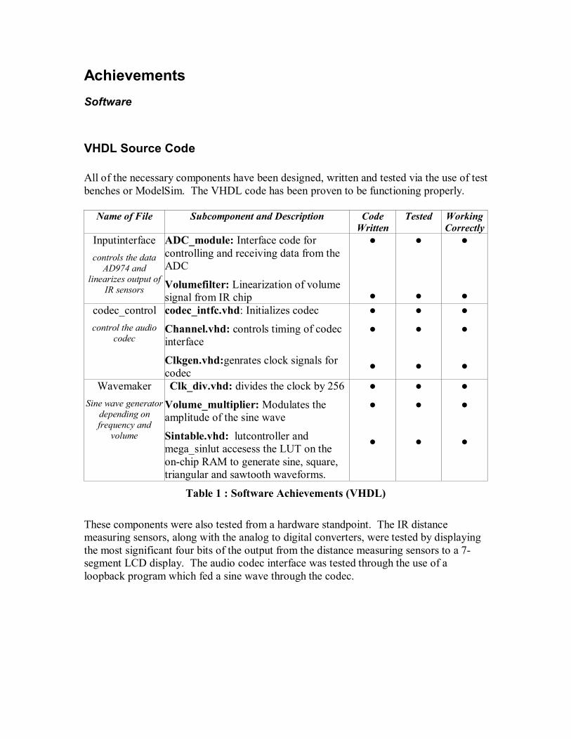
Achievements Software
VHDL Source Code All of the necessary components have been designed, written and tested via the use of test benches or ModelSim. The VHDL code has been proven to be functioning properly.
Name of File Subcomponent and Description Code Written
Tested Working Correctly
Inputinterface controls the data
AD974 and linearizes output of
IR sensors
ADC_module: Interface code for controlling and receiving data from the ADC
Volumefilter: Linearization of volume signal from IR chip
codec_control control the audio
codec
codec_intfc.vhd: Initializes codec
Channel.vhd: controls timing of codec interface
Clkgen.vhd:genrates clock signals for codec
Wavemaker Sine wave generator
depending on frequency and
volume
Clk_div.vhd: divides the clock by 256
Volume_multiplier: Modulates the amplitude of the sine wave
Sintable.vhd: lutcontroller and mega_sinlut accesess the LUT on the on-chip RAM to generate sine, square, triangular and sawtooth waveforms.
Table 1 : Software Achievements (VHDL) These components were also tested from a hardware standpoint. The IR distance measuring sensors, along with the analog to digital converters, were tested by displaying the most significant four bits of the output from the distance measuring sensors to a 7-segment LCD display. The audio codec interface was tested through the use of a loopback program which fed a sine wave through the codec.

Matlab Scripts for the Generation of Waveforms
Through the use of Matlab, binary sine, square, triangle and sawtooth waves were created and stored in the on-chip RAM. The RAM had a length of 256 and a width of 12 bits. The binary data output by the scripts is plotted.
Name Description Written Tested Working correctly
Binarysawtooth.m Generates a binary square wave. Binarysine.m Generates a binary sine wave. Binarysquare.m Generates a binary square wave. Binarytriangle.m Generates a binary triangular
wave.
Table 2 : Matlab scripts
Overall System Functionality Variation of Pitch of the Instrument The user is able to vary the frequency emitted by the Theremin from a minimum of 980.00 Hz to a maximum of 2.94 kHz by moving their hand from a 10 cm to 80 cm distance from the pitch control IR sensor. Variation of Volume of the Instrument The user is able to successfully control the volume of the instrument by moving their hand from a 10 cm to 80 cm distance from the IR sensor responsible for pitch control. Selection of Wave Shape Through the use of two DIP switches located on the board, the user is able to select from a square, sine, sawtooth and triangular waveform. Each of these waveforms produced a different sound. Sustain Pitch Switch A push button enables the user to hold the current frequency which is emitted by the instrument.

Description of Operations
Block Diagram of Data Flow
GP2YOA21YKDistance
MeasuringSensor
ADC974Analog to DigitalConverter (16-bit)
VolumeModulator
InputInterface(serial-parallel
conversion,ADC control)
OutputInterface
(parallel-serial conversion,
Codec control)
SustainFrequency
Switch
WaveShape
Selector
Look Up Table(for frequency/wave shape)
selection
PhaseAccumulator
ADC974Analog to Digital
Converter (16-bit)
GP2YOA21YKDistance
MeasuringSensor
InputInterface(serial-parallel
conversion,ADC control)
20-bit stereo audio codec
to speaker
XSA-100 Spartan-II
Prototyping Board
MC33172POperational
Amplifier
MC33172POperational
Amplifier
Figure 1 : Block Diagram of Data Flow
System Clock
The frequency of the system clock is 12.5MHz. This is used in order to be able to use the audio codec. The sampling frequency for the codec is 256 times slower than the system clock. With a clock frequency of 12.5MHz, the sampling rate is 48.8kHz which satisfies Nyquist's criteria.
Input Sensor
The theremin will be implemented using IR sensors to measure the distance of the musicians hand from the instrument. The left hand will control the pitch and the right hand will control the volume. The IR sensors, which will be used for this purpose are GP2Y0A21YK from Sharp. (See data sheet attached). The range of analog output voltage of the sensor is 0.4V to 2.4V for detecting distance of 80cm to 10 cm, which is appropriate for the theremin. Also, the sensor is not as influenced by the color of

reflective objects or their reflectivity as other IR sensors since it uses an angle measurement for calculating distance.
Processing of the inputs
The output of the sensors is an analog voltage. This analog voltage will be converted to digital voltage by a 16- bit Analog to Digital converter (ADC). The range of analog output of the sensors is 0.4V to 2.4V. Since we are operating the ADCs with a 5V supply, the resolution of the ADC is 76uV per bit. This gives a potential digital range from 0x148F to 0x7B5B. The ADC puts out serial data.
Pitch and Volume control
The pitch and volume control of the theremin come from the output of the two ADCs. This data will be converted to parallel signals and used by the NCO. The pitch control signal will be used as the input word to the NCO. The volume control signal will be used as a multiplicand in a multiplier for signal amplification.
Wavemaker Module
The wavemaker module is a numerically controlled oscillator (NCO) that generates a output waveform whose frequency and magnitude varies according to the 8 bit frequency and volume inputs. One of 5 waveforms can be selected using the 3 bit sound_select input. The waveforms are stored in Block RAM.
Wavemaker Module Generalized Block Diagram
Figure2: Wavemaker Block Diagram
Sintable Module
The Sintable module generates an output waveform whose frequency varies according to
Lut_Controller
Lut1 Lut2 Lut3 Lut4 Lut5
Sintable
Multiplier
Sound_select
Frequency
Volume
Wavemaker
Output
Waveform
Block RAM
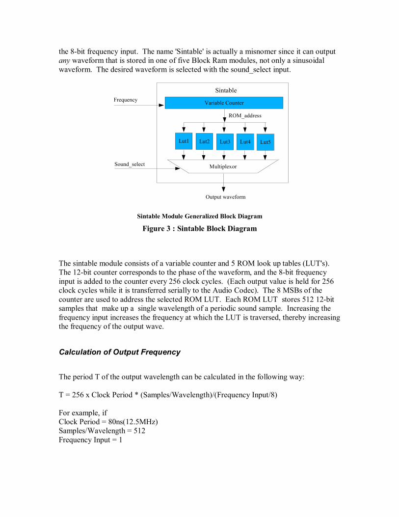
the 8-bit frequency input. The name 'Sintable' is actually a misnomer since it can output any waveform that is stored in one of five Block Ram modules, not only a sinusoidal waveform. The desired waveform is selected with the sound_select input.
Sintable Module Generalized Block Diagram
Figure 3 : Sintable Block Diagram
The sintable module consists of a variable counter and 5 ROM look up tables (LUT's). The 12-bit counter corresponds to the phase of the waveform, and the 8-bit frequency input is added to the counter every 256 clock cycles. (Each output value is held for 256 clock cycles while it is transferred serially to the Audio Codec). The 8 MSBs of the counter are used to address the selected ROM LUT. Each ROM LUT stores 512 12-bit samples that make up a single wavelength of a periodic sound sample. Increasing the frequency input increases the frequency at which the LUT is traversed, thereby increasing the frequency of the output wave.
Calculation of Output Frequency
The period T of the output wavelength can be calculated in the following way: T = 256 x Clock Period * (Samples/Wavelength)/(Frequency Input/8) For example, if Clock Period = 80ns(12.5MHz) Samples/Wavelength = 512 Frequency Input = 1
Variable Counter
Lut1 Lut2 Lut3 Lut4 Lut5
MultiplexorSound_select
Frequency
ROM_address
Sintable
Output waveform

The output wavelength frequency f = 1/T = 11.92 Hz. This also corresponds to the frequency resolution. For a frequency input = 255 (the maximum for an 8 bit input) f = 1/T = 3040 Hz. This corresponds to the maximum output frequency of the sintable module.
Output processing
The output of the volume modulator will be sent to a parallel to serial converter, which will be coded and downloaded to the FPGA. Its output will be sent to the stereo audio codec on the Xstend board. The stereo codec accepts serial bit stream from the XS board which converts it into two analog output signals. These signals will be fed into an amplifier and output through a speaker

Diagram of Design Hierarchy
Figure 4 : Design Hierarchy Diagram
thereminthe project
theremin_pkg
IpinterfaceSends control signals to
and receives input from AD974.
WavemakerGenerates wave based on
frequency and volume.
codec_controlOutputs generated wave
to stereo codec.
ipinterface_pkgcodec_pkg
ADC_module
hex_display
Volumefilter
Wavemaker_pkg
Clk_div
Multiplier
Sintable
Sintable_pkg
Lutcontroller
mega_sinlut
Dec3to8
Sinlut1
Sinlut2
Sinlut3
Sinlut4
Codecintfc
Clkgen
Channel

Theremin Data Sheet
Block Diagram
GP2YOA21YKDistance
MeasuringSensor
ADC974Analog to DigitalConverter (16-bit)
VolumeModulator
InputInterface(serial-parallel
conversion,ADC control)
OutputInterface
(parallel-serial conversion,
Codec control)
SustainFrequency
Switch
WaveShape
Selector
Look Up Table(for frequency/wave shape)
selection
PhaseAccumulator
ADC974Analog to Digital
Converter (16-bit)
GP2YOA21YKDistance
MeasuringSensor
InputInterface(serial-parallel
conversion,ADC control)
20-bit stereo audio codec
to speaker
XSA-100 Spartan-II
Prototyping Board
MC33172POperational
Amplifier
MC33172POperational
Amplifier
Figure 5 : Block Diagram of Data Flow
Features
!Both volume and frequency control !Produces sine, sawtooth, triangular, square, and synth audio signals !Output frequencies vary from 980Hz to 2.9 Khz !Frequencies are produced using the Direct Digital Synthesizer (DDS) method !Utilizes an IR Distance Measuring Sensor from Sharp !Employs a Fast 16-Bit ADC with 200 kSPS Throughput From Analog Devices !ADC operates at a 48kHz sampling rate !Controlled from a Xlinx Spartan II FPGA running on a Xess XSA Board !Utilizes 256K × 16 of RAM and 5 blocks of 256K × 16 ROM
General Description
The Theremin is a musical instrument which can be played without physical contact. The Theremin utilizes two Sharp IR sensors to measure the distance of a players hand to vary the pitch and volume of the output. The Theremin can produce several different output
High Tech Musical Instrument

waveforms including sine, sawtooth, and square waves. The controller of the Theremin is implemented on a Spartan II FPGA which is embedded on a XESS XSA board. An Analog Devices AD974 analog to digital converter is used to convert the signal from the IR sensors to 16 bit digital data at a 48kHz sampling frequency. The digital output from the FPGA is converted to analog by way of a 20 bit DAC provided on the XSA board. The Theremin operates off a single +9V power supply. The Theremin produces output frequencies via the Direct Digital Synthesizer (DDS) method. Waveforms are stored in lookup tables from which the frequency can be varied by skipping samples in the table. As more samples in the LUT are skipped the frequency of the output signal will increase. The Theremin is fabricated using EE552s patented no sleep process.
Parameter Condition Min Typ Max Units IR Sensor Characteristics Detecting Distance 10 80 cm Distance Measurement Sampling Rate
26 Hz
Output Voltage (no load)
0 3.5 volts
ADC Characteristics Resolution 16 bits Bit Rate 12.5 Mbits/sec Sampling Rate 48 kHz Input Voltage 0 4 volts FPGA Characteristics # of logic blocks 327 volts ROM 5 Blocks of 256k
by 16 Maximum speed 9.1 ns Overall Characteristics Output frequency range
0.98
2.9
kHz
Table 3 : Characteristics
I/O Pin Descriptions
Common pins to all interfaces
FPGA pins Signal name Description 88Clock: in Stepped down clock at 12.5 MHz 26Reset : in Reset pushbutton on the XSA board
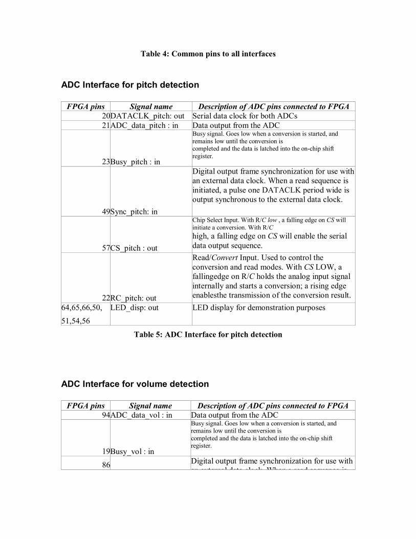
Table 4: Common pins to all interfaces
ADC Interface for pitch detection
FPGA pins Signal name Description of ADC pins connected to FPGA 20DATACLK_pitch: out Serial data clock for both ADCs 21ADC_data_pitch : in Data output from the ADC
23
Busy_pitch : in
Busy signal. Goes low when a conversion is started, and remains low until the conversion is completed and the data is latched into the on-chip shift register.
49
Sync_pitch: in
Digital output frame synchronization for use with an external data clock. When a read sequence is initiated, a pulse one DATACLK period wide is output synchronous to the external data clock.
57
CS_pitch : out
Chip Select Input. With R/C low , a falling edge on CS will initiate a conversion. With R/C high, a falling edge on CS will enable the serial data output sequence.
22
RC_pitch: out
Read/Convert Input. Used to control the conversion and read modes. With CS LOW, a fallingedge on R/C holds the analog input signal internally and starts a conversion; a rising edge enablesthe transmission of the conversion result.
64,65,66,50, 51,54,56
LED_disp: out LED display for demonstration purposes
Table 5: ADC Interface for pitch detection
ADC Interface for volume detection
FPGA pins Signal name Description of ADC pins connected to FPGA 94ADC_data_vol : in Data output from the ADC
19
Busy_vol : in
Busy signal. Goes low when a conversion is started, and remains low until the conversion is completed and the data is latched into the on-chip shift register.
86 Digital output frame synchronization for use with an external data clock When a read sequence is

FPGA pins Signal name Description of ADC pins connected to FPGA
Sync_vol: in
an external data clock. When a read sequence is initiated, a pulse one DATACLK period wide is output synchronous to the external data clock.
13
CS_vol : out
Chip Select Input. With R/C low , a falling edge on CS will initiate a conversion. With R/C high, a falling edge on CS will enable the serial data output sequence.
12
RC_pitch: out
Read/Convert Input. Used to control the conversion and read modes. With CS LOW, a fallingedge on R/C holds the analog input signal internally and starts a conversion; a rising edge enablesthe transmission of the conversion result.
Table 6: ADC Interface for volume detection
Output interface to Stereo Codec
FPGA pins Signal name Description 77Mclk:out This output is the master clock for the codec chip.
75Sclk:out This output is the clock for synchronizing serial
data transfers between the FPLD and the codec.
59Lrclk:out This output controls the activation of the left and
right channel circuitry in the codec.
76Sdin:out The serial data stream for the codec DAC is
shifted out through this output.
Table 7 :Output interface to Stereo Codec
Other Pins
FPGA pins Signal name Description
111 foot_pedal This input will hold the volume and pitch at their
current values.
68,44switch This switch will be used to select between 4
different kinds of waves
Table 8 :Other pins used in the project

Wave Selection
Switch Description '000' Sine wave '001' Sawtooth wave '011' Square wave '100' Triangle wave
Table 9 : Swich Descriptions
Timing Specifications
External Components
Component Description Maximum Sampling Frequency
GP2Y0A21YK Distance measuring sensor. 26.1 HzAD974 16-bit serial analog to digital
converter. 200 kHz
Xstend Codec 20-bit stereo audio codec. 46.875 kHz
Table 10 : External Components
Internal Components
Component Name Maximum Clock Frequency Codec control 108.59 MHzIP interface 110.14 MHzWavemaker 73.41 MHzTheremin 65.41 MHz
Table 11 : Internal Components The Sharp GP2Y0A21YK General Purpose Distance Measuring Sensors have the lowest frequency of all the components and is thus the limiting factor in the determination of the maximum frequency of the Theremin. Chip Performance and Resources

Resource Requirements: Memory Utilization and Timing Analysis
Table 12 : Resource Requirements Results of Experiments and Characterization Input Interface
It was necessary to characterize the output of the IR sensor for consideration in the design of the firmware part of the project. The following figure shows the output voltage of the IR sensor versus the distance of a hand from the sensor.
ComponentTheremin 327 15.289ns 65.407MHz Codec Control 47 9.209ns 108.589MHz IPInterface 79 9.079ns 110.144MHz ADC_Module 32 Hex_Display 4 Wavemaker 250 13.623ns 73.405MHz Clk_Div 40 Multiplier 50 Sintable 137 LUT_Controller 52 Mega_sinlut 40 Dec3to8 4
Sinlut1-5(Block RAM) 5 x 512K * 16bits = 4096Kbits
Logic Slices Required
(1200 Total Available)
Minimum Clock Period (Post Place &
Route) (ns)
Maximum Clock Frequency (Post Place & Route)
(Mhz)

IR Sensor Output V oltage vs. Distance Fr om Sensor
0.000
0.500
1.000
1.500
2.000
2.500
3.000
3.500
4.000
0 3 5 8 13 17 23 27 33 37 43 47 55 65 75 85
Distance (cm )
Outpu
t Volt
age (
V)
Figure 6: IR Sensor Voltage vs Distance The sensor output is not linear and it resembles a decaying exponential. This will make accurately reading the output at the higher distances difficult because the resolution is so low. An ADC of 16-bits was chosen to try to be able to measure this low resolution. The sensor was connected to the ADC and a test program was written to make sure the data was being received. The top four bits of the ADC were put onto a seven segment LED display as hex values. These values were seen to vary as the voltage of the sensor was varied.
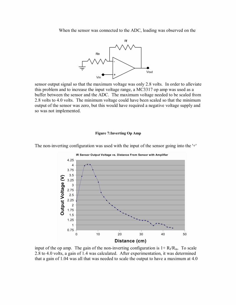
When the sensor was connected to the ADC, loading was observed on the
sensor output signal so that the maximum voltage was only 2.8 volts. In order to alleviate this problem and to increase the input voltage range, a MC3317 op amp was used as a buffer between the sensor and the ADC. The maximum voltage needed to be scaled from 2.8 volts to 4.0 volts. The minimum voltage could have been scaled so that the minimum output of the sensor was zero, but this would have required a negative voltage supply and so was not implemented.
Figure 7:Inverting Op Amp
The non-inverting configuration was used with the input of the sensor going into the '+'
input of the op amp. The gain of the non-inverting configuration is 1+ Rf/Rin. To scale 2.8 to 4.0 volts, a gain of 1.4 was calculated. After experimentation, it was determined that a gain of 1.04 was all that was needed to scale the output to have a maximum at 4.0
0 10 20 30 40 500.75
11.25
1.51.75
22.25
2.52.75
33.25
3.53.75
44.25
IR Sensor Output Voltage vs. Distance From Sensor with Amplifier
Distance (cm)
Out
put V
olta
ge (V
)-
+
Rin
Rf
Vin
Vout

volts at the input to the ADC. The resistor values chosen were 104Ω and 4Ω. The resulting voltage vs. distance graph can be seen in Figure 2. The op amp did not increase the resolution as hoped but it did provide buffering into the ADC.
Figure 8: IR Sensor Voltage vs. Distance from Sensor with Amplifier The output voltage of the IR sensor was found to fluctuate by as much as half a volt. It was thought that this was being caused by noise on the power supply line caused by the ADC. Upon scoping the 5V supply shared by the IR sensor and the ADC we noticed a dip in the voltage up to 0.88V in amplitude, repeating at a frequency of 980Hz. This is suspiciously similar to the minimum output frequency but no correlation was able to be determined between these two facts. When the ADC was disconnected and the power supply was connected directly to the IR sensor, its output voltage no longer fluctuated. To remedy the power supply voltage noise, a 2.2µF capacitor was added to the 10µF and 0.1µF capacitors already being used to filter the supply voltage. However, the extra capacitor did not make a difference. While testing the ADC it was noticed that even when the power supply was shut off, there was 2 volts on the power line of the breadboard that the ADC and IR sensor are on. Upon further testing it became obvious that this power was being supplied by the control signals of the FPGA and was propagating through VDIG (digital voltage supply) of the ADC onto the power line. This characteristic of the ADC did not seem to be causing any problems and had no immediate solution other than changing ADC chips, and so it was left as is.
All control and data signals for the ADC are carried to and from the FPGA by way of a ribbon cable. However, this ribbon cable has a large amount of capacitance which had some negative effects. Namely, it caused problems on the data line where logic high signals were just barely able to get above the logic high threshold during the sampling period.
Output Interface
Since sound must be produced at the final output, a converter from a digitally encoded wave to an analog sound wave must be used. Fortunately, there is one built into the development board that is being used for this project. The audio codec chip that is being used is the AKM AL4520A 20-bit stereo ADC & DAC. The XESS company that makes the development board has a sample program called loopback on their website that takes in audio data from the ADC and puts it back onto the DAC unaltered. This program was used as the initial test for the audio codec. The loopback program compiled nicely but the pin assignments were a problem. The assignments given in the documentation were wrong for the board that is being used for this project. So the correct assignments had to be found and put in the user contraints file. After this was done, the program worked as expected. When a

portable CD player was attached to the input jack and a mini-speaker was attached to the output, the cool tunes of Depeche Mode were enjoyed by all. The sounds that the theremin produces are generated internally and so the loopback program had to be modified in order to be able to be used for this project. A simple program that created a repetative waveform internally was used to test the feasibility of an internally generated wave.
Wavemaker Module
The wavemaker module consists of a clock divider (clk_div.vhd), Numerically Controlled Oscillator (sintable.vhd) and a multiplier. Clock Divider: Using 'False' Clocks The clock divider module is used so that each output value of the wavemaker module is held for 256 clock cycles as it is transferred serially to the Audio Codec. Originally, the clock divider module was actually a clock divider, and the clock input of all wavemaker modules was a slower version of the system clock. However, it was found that using a 'false' clock could result in glitches and clock skew problems when the wavemaker modules were interfaced with external modules. So, the clock divider's 'slow_clk' output was instead routed to the enable inputs of the various wavemaker modules. The behaviour of the wavemaker module became more stable and predictable. Using RAM: Distributed vs. Block RAM RAM is used to store the sound samples for the Numerically Controlled Oscillator. Two types of on-chip RAM were investigated and implemented, and the implementation results compared; Distributed RAM and Block RAM. Both types of RAM were designed using the Xilinx Core Generator tool. Distributed RAM. Distributed RAM is implemented using on-chip configurable logic blocks (CLB). The disadvantage of using logical blocks as memory elements is that it uses logical resources that may be required for other logical or arithmetic modules. Block RAM. Each Spartan II FPGA contains 10 256K x 16 bit dedicated ROM Blocks, for a total of 4096 Kbytes of on-chip memory. This amount of memory was sufficient for our purposes. Using ROM Blocks conserves CLB's for other modules that may need them. 5 Blocks of 256 * 12 bits of memory (1.92 Kbytes) was allocated using Distributed and Block Memory. The results are shown below.

Resource Requirements of Distributed and Block RAM for a SPARTAN II FPGA
Logical Slices Used /ROM Blocks Used Component Distributed RAM Block RAM
Theremin 899/0 327/5Wavemaker 731/0 250/5 As can be seen in the table above, 481 fewer logical slices were used in the version of the Sintable module that used BLOCK RAM. So, 1 Kbyte of RAM(ROM) corresponds to 480/1.92Kbytes = 250 Logical Slices. The savings in logical elements is significant, considering that there are only 1200 logical slices available on the SPARTAN II FPGA.
Integrated Project
Preliminary experimentation was done by hardcoding simulated frequency and volume values into the full design. When this was done, the wave look up tables performed as expected and the different waveforms were heard at the output. Once the preliminary testing was performed the input interface was connected. Initial testing was conducted empirically by listening to the output. The theremin was found to work somewhat as expected with a frequency that varied with the movement of the players hand. However, there were noticeable unwanted frequencies present in the output tone. It was observed that at one frequency all the noise disappeared and a pure tone was heard. From this knowledge, it was determined that the unwanted noise was caused by the input from the sensors switching too rapidly. Many attempts were made to try to rectify this problem: A lowpass filter was used between the output of the sensor and the input of the ADC.
This helped the problem but decreased the resolution substantially. All bits except for the most significant 2 were truncated. By doing this, four different
discreet levels were heard. But in the transition region, the signals were still very noisy. On the oscilloscope, it could be seen that the wave changed frequency faster than it could complete a full wavecycle. With the wave switching between frequencies like this, higher frequency components got put in the signal. Thus, it was assumed that this was the problem with the signal with more significant bits as well.
A delay was put into the ADC controller to delay how often it sent data to the FPGA. This seemed to help a bit but it still was switching quite rapidly in the transition regions.
An averaging component was used to smooth out the data from the ADC. This provided the biggest improvement in signal quality. The values for delay and number of averages taken were then tweaked to provide the best quality sound.
The range of frequencies that could be produced also had to be adjusted to get the greatest range with the smallest frequency increment. This was done by changing the phase accumulator width and the width of the frequency control word.

Externally Provided HDL Elements The externally provided HDL component used in this project comes from XESS corporation. They have provided a module called codec_intfc for controlling the audio codec on the Xtend board. They use this module in a program called loopback.vhd which takes a stereo audio signal from the input jack and plays it back to the output jack. Since the theremin does not need to use the ADC on the codec, the portion for reading in data from the ADC can be taken out.

References 1.AD974: 4-Channel, 16-bit 200 kSPS Data Acquisities System. Copyright 1999 by
Analog devices. http://ww.analog.com.
2.Arbitrary Waveform Generates & Function Generators. Copyright 2001 by K. Yokogawa. Http://www.yokogawa.com/tm/GC/fg/fg_overview.pdf.
3.Direct Digital Synthesizer with an On-Chip D/A-Converer, IEE Journal of Solid-State Circuits, Vol. 33, no. 2. Copyright February 1998 by Jouka Vankka. Http://clsi2.kaist.ac.kr/project/ddfs_paper/33ssc02-vankka.pdf.
4.EE 552 Application Notes: 2-D Mapper. Copyright 1998 by Shaun Luon, Clifton Yeung, J.P. Kansky and Patrick Asiedu-Ampem. Http://www.ee.ualberta.ca/~elliott/ee552/projects/1998f/2-DMapper/transmit.vhd
5.GP@Y0A21YK: General Purpose Type Distance Measuring Sensors. Copyright 2003 by Sharp Semiconductors. Http://www.sharpsma.com.
6.XSA Board v. 1.1, 1.2 User Maual: How to Install, Test and Use Your New XSA Board. Copyright May 2002 by XESS Corporation. Http://www.xess.com/manuals/xsa-manual-v1_2.pdf
7.Xstend Board V1.2.2 Manual: How to Install and Use Your New Xstend Board. Copyright May 2001 by Xess Corporation. Http://www.xess.com/mauals/xst-manual-v_1_3_2.pdf.