Embed Size (px)
Citation preview

Final Progress Report of UGC Major Research
Project for the period 01/04/2013 to 31/03/2017
Title of the research project:
Synthesis and characterization of V2-VI3 compound in single
crystal/nanomaterial/thin film forms
Reference: UGC Major research project vide.
Sanctioned letter F. No. 42-826/2013 (SR)
Dated: 22nd March, 2013
Principal Investigator: Prof. M. P. Deshpande
Department of Physics
Sardar Patel University
VallabhVidyanagar, Anand
Gujarat-388120

ANNEXURE-III
P. G. Department of Physics
Sardar Patel University
Vallabh Vidyanagar- 388120
STATEMENT OF EXPENDITURE IN RESPECT OF MAJOR RESEARCH PROJECT
1. Name of Principal Investigator : Prof. M. P. Deshpande
2. Department of Principal Investigator : Department of Physics,
University : Sardar Patel University,
Vallabh Vidyanagar- 388 120,
Gujarat, INDIA
3. UGC approval Letter No. and Date: F.No.42-826/2013 (SR) dated 22nd
March, 2013
4. Title of the Research project: “Synthesis and characterization of V2-VI3
compound in single crystal/nanomaterial/thin film forms”
5. Effective date of starting the project : 1st April 2013
6. a. Period of Expenditure : From 01/04/2013 to 31/03/2014 (1st Year)
01/04/2014 to 31/03/2015 (2nd
Year)
01/04/2015 to 31/03/2016 (3rd
Year)
01/04/2016 to 31/03/2017 (extended Year)
b. Details of Expenditure :
Sr.
No. Item
Amount
Approve
d (Rs.)
Expenditure Incurred (Rs.)
01/04/2013
to
31/03/2014
(1st Year )
01/04/2014
to
31/03/2015
(2nd
Year)
01/04/2015
to
31/03/2016
(3rd
Year)
01/04/2016
to
31/03/2017
(ext. Year)
Total
i
Equipments
(SILAR
control
system,
Bridgman
mechanical
set up)
4,00,000 3,58,620 - - 3,58,620
ii Contingency 50,000 5,155 6,025 14,995 7,895 34,070

iii
Field
Work/Travel
(Give details
in the
proforma at
Annexure-
IV).
15,000 1,280 7,440 2,188 - 10,908
iv Chemicals &
Glassware 60,000 16,725 12,973 - - 29,698
v Overhead 63,800 63,800 - - - 63,800
Total (Rs.) 5,88,800 4,45,580 26,438 17,183 7,895 4,97,096
c. Staff : Miss. Kamakshi R. Patel (Project Fellow)
Date of Appointment : 1st July 2013
S. No. Items From
Amount
Approved
(Rs.)
Expenditure
incurred
(Rs.)
1 Project Fellow @Rs.
14,000/-p.m.
1st
July 2013
to
31st March 2014
5,28,000/-
1,12,000/-
2 Project Fellow @Rs.
14,000/-p.m.
1st April 2014
to
31st March 2015
1,68,000/-
3
Project Fellow @Rs.
14,000/-p.m.
Project Fellow @Rs.
16,000/-p.m.
1st April 2015
To
June 2015
1st July 2015
To
31st March 2016
2,00,000/-
4 Project Fellow @Rs.
16,000/-p.m.
1st April 2016
To
June 2016
48,000/-
Total (Rs.) 5,28,000/-

Annexure –VIII
P.G. Department of Physics
Sardar Patel University
Vallabh Vidyanagar- 388120 Report of the work done on the Major Research Project
1. Project report No. : Final
2. UGC Reference No. : F.42-826/2013 (SR)
3. Period of report from : 01/04/2013 to 31/03/2014 (1st Year)
01/04/2014 to 31/03/2015 (2nd
Year)
01/04/1015 to 31/03/1016 (3rd
Year)
01/04/1016 to 31/03/1017 (extended Year)
4. Title of research project : “Synthesis and characterization of V2-VI3compound in single
crystal/nanomaterials/thin film forms”
5. (a) Name of the Principal Investigator: Prof. M. P. Deshpande
(b) Deptt. : Department of Physics
(c) University/College where work has progressed: Sardar Patel University,
VallabhVidyanagar-388120,
Gujarat, INDIA
6. Effective date of starting of the project : 01/04/2013
7. Grant approved and expenditure incurred during the period of the report:
a. Total amount approved: Rs. 11, 16, 800.00
b. Total expenditure: Rs.10, 25, 096/-
(Rs. 5, 57,580/- (1st Year) +Rs. 1, 94,438/- (2
nd Year) + Rs. 2, 17,183/-(3
rd Year) +
Rs. 55,895/- (extended Year 01/04/2016 to 31/03/2017) = Rs.10, 25, 096/-)
c. Report of the work done: See Enclosure - I
i. Brief objective of the project
a. Synthesis and characterization of V2-VI3 compound in single crystal/ nanomaterials/ thin
film forms
b. Characterization of synthesized compound
c. Study on structural, optical and thermal properties.
ii. Work done so far and results achieved and publications, if any, resulting from the work (Give
details of the papers and names of the journals in which it has been published or accepted
for publication……
(1) Sb2S3 microspheres prepared by solvothermal method
M. P. Deshpande, Pallavi Sakariya, Sandip V. Bhatt, Kamakshi R. Patel, Nikita H. Patel,
S. H. Chaki.
Advance Science Letters, 20, (2014), 1102 -1106.

Enclosure - I
The literature survey of the project work on V2-VI3 semiconducting materials in different forms
have been collected as per the proposal submitted from internet as well as from library.
Necessary chemicals and glassware has been purchased during this year of the project. The
equipment sanctioned in the mentioned project, SILAR controller and Bridgman mechanical set
up are purchased from Holmarc Opto-Mechatronics (P) Ltd. Instruments, Kochi, Kerala and Vi
Micro Systems Pvt .Ltd. Perungudi, Chennai respectively which are shown in figure 1. Efforts
are underway to prepare thin films by SILAR technique. We have started to calibrate high
temperature dual zone furnace with the facility available in the department for the growth of
single crystals by Bridgman in the required temperature range by applying the range of trials.
Bridgman mechanical set up SILAR control unit
Figure 1 Photograph of equipments purchased
The equipments are installed and working satisfactorily. The project fellow has been trained
accordingly to the requirement of project.
In continuation with the above work, in next duration we have synthesized single crystal of
Sb2S3 by chemical vapor transport technique, microsphere of Sb2S3 by solvothermal method,
Sb2S3 thin film by SILAR coating unit and Bi2S3 nanorods prepared at room temperature and
studied their various properties by different characterization techniques.
The complete description of this work is described below.
Single crystals of Sb2S3
(A) Growth method
Single crystals of Sb2S3 were prepared from high purity (99.999%) antimony (Sb) and sulfur (S)
powder. First of all, the powder were weighed and loaded into thick walled quartz ampoule. The
ampoule was then evacuated (10-5
torr) and sealed and then placed in the horizontal single zone
furnace to prepare charge at500°C for 3 days. The prepared charge was taken in another quartz
ampoule with NH4Cl used as a transporting agent and then again sealed at 10 -5
torr and placed in
the dual zone furnace at temperature 500°C to 450°C of the source zone and growth zone
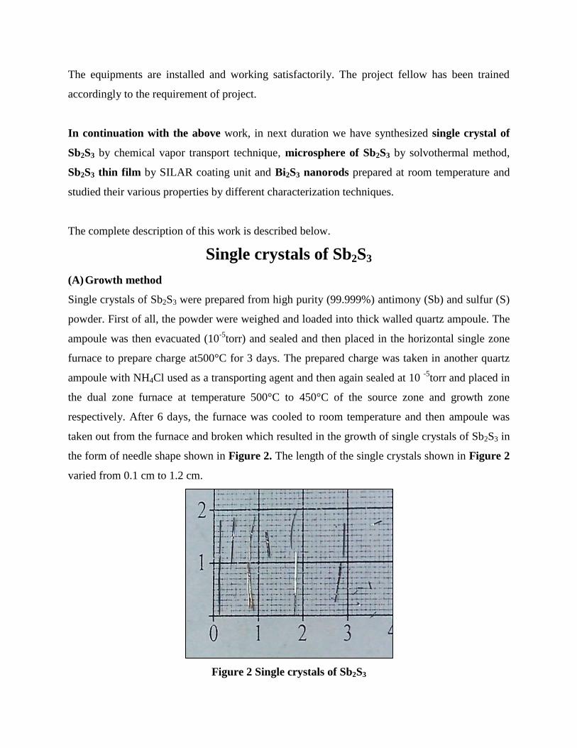
respectively. After 6 days, the furnace was cooled to room temperature and then ampoule was
taken out from the furnace and broken which resulted in the growth of single crystals of Sb2S3 in
the form of needle shape shown in Figure 2. The length of the single crystals shown in Figure 2
varied from 0.1 cm to 1.2 cm.
Figure 2 Single crystals of Sb2S3

(B) Characterization
1. Energy Dispersive Analysis of X rays (EDAX)
Figure 3 EDAX spectra of Sb2S3 single crystal
The composition of the grown crystals determined from the EDAX spectra shown in figure 3 are
shown in the below table 1.
Table 1 wt % of the elements
Composition Element Wt% (obtained) Wt% (calculated)
Sb2S3 Sb 72.20 71.68
S 27.80 28.32
2. X-ray diffraction
X-ray diffraction pattern of Sb2S3 powder (polycrystalline) made from single crystals is shown in
figure 4. All the diffraction peaks shown in figure 4 were indexed with the help of powder-X
software to pure orthorhombic phase of Sb2S3 with calculated lattice parameters: a = 11.239 Ao,
b = 11.313 Ao and c = 3.841 A
o.

Figure 4 X- ray diffractogram of Sb2S3 compound
The results are in good agreement with standard data card (JCPDS 42-1393) [1] and previously
reported data for Sb2S3 [2,3] We have used Scherrer’s formula [4] to calculate the crystallite size
for various reflections and it indicates that these sizes vary between 23Ao
to 65Ao. The sharp
diffraction peaks are an indication of good crystallinity of Sb2S3sample.
3. Scanning Electron Microscopy (SEM)
The surface morphology of grown single crystals of Sb2S3 at different magnification of 100X,
50X and 500X using SEM are shown in below figures 5 (a,b),(c,d),(e,f) respectively. It is seen
that crystals surfaces are possessing cracks and visible inclusions.

Figure 5 SEM photographs of Sb2S3
4. Raman spectroscopy
Figure 6 shows the Raman spectrum of Sb2S3 single crystal at room temperature using Ar laser
source.
Figure 6 Raman spectra of Sb2S3 single crystal
This exhibits seven resonant peaks at about 115, 147, 190, 252, 282, 300 and 373 cm-1
in the
range of 100 - 400 cm-1
. The presence of sharp peaks at 190 and 252 cm-1
suggests the formation

of well crystalline product [5]. The low intensity peaks at 282, 300 and 373cm-1
can be assigned
to the unit Sb2S3 pyramid of the material having C3v symmetric mode [6]. All these results are in
good agreement with the reported Raman spectrum [7].At room temperature Sb2S3 crystallizes in
orthorhombic form with four molecules and 20 atoms per unit cell, stibnite has 60 normal modes,
which according to the group theory decompose in Γ as
10Ag+5B1g+10B2g+5B3g+5Au+10B1u+5B2u+10B2u. The acoustic modes have character
B1u+B2u+B3u. The Au modes are silent whereas all the other modes are active. The optical modes
are distributed over a narrow0-350 cm-1
frequency range. The infrared reflectivity spectrum
shows a multitude of peaks which are poorly differentiated and highly overlapping. The Raman
spectrum is better differentiated with five main peaks. The main infrared mode lies around 246
cm-1
and represents as upper position of at least one B3u and one B1u modes [8].
5. TGA analysis
Figure 7 shows the TGA curve of Sb2S3 crystal under nitrogen (N2) atmosphere. It is observed
from thermogram that Sb2S3 decomposes slowly from 27°C to 472°C having small weight loss
of nearly 2%.
Figure 7 TGA spectra of Sb2S3 crystal powder under N2 atmosphere
The continuous decomposition occurs after 472°C to 575°C, which shows weight loss of nearly
5%. From the TGA curve, we have calculated the activation energy in the weight loss region
(which is nearly 5%) by using three models viz Broido relation (BR), Piloyan-Novikova (PN)
relation and Coats Redfern (CR). Values of calculated activation energy for three different
models are given in the table 2. Since the electrical resistance of Sb2S3 material is very high in

the order of MegaOhm, therefore, measurement of electrical resistivity, thermoelectric power
and Hall Effect of Sb2S3 could not be measured. We determined only thermal conductivity of
Sb2S3 crystal pellet at 100°C and it comes out to be 0.422 Wcm-1
deg-1
. Thus we were not able to
calculate the figure of merit of Sb2S3 single crystal, so as to prove its utility for thermoelectric
material.
Table 2 activation energy for the Sb2S3 single crystal
Microspheres of Sb2S3
(A) Synthesis of Sb2S3 microsphere using solvothermal Method
All of the chemical reagents used in this experiment were of analytical grade and were used
without further purification. In a typical procedure, 0.23 g antimony chloride (SbCl3) and 0.45 g
tartaric acid were dissolved in 16 mL N, N-dimethyl formamide (DMF). In this solution about
0.244 g sulfur powder was added with stirring. This mixed solution was transferred into a
Teflon-lined stainless steel autoclave. The autoclave was sealed and maintained at 120oC for 4 h
and then cooled to room temperature naturally. The precipitates were collected and washed with
distilled water for several times. Then, the precipitates were dried in air. Finally, the resultant
burgundy colored powder sample which is shown in figure 8 were obtained and characterized by
various techniques.
Figure 8 Microspheres of Sb2S3
Name of model Broido relation Piloyan-Novikova
relation
Coats-Redfern
relation
Activation energy 0.97eV 0.38eV 0.38eV
(B) Characterization
1. Energy Dispersive Analysis of X-rays (EDAX)
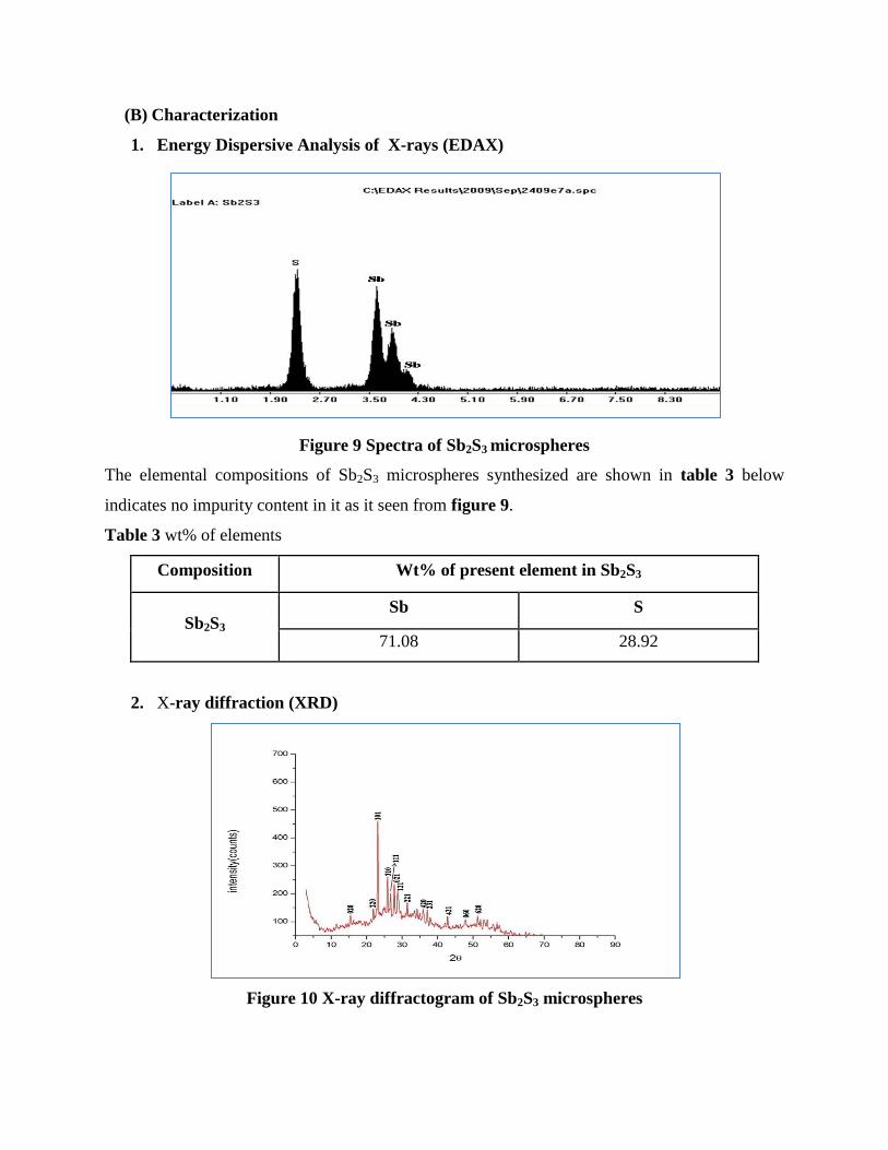
Figure 9 Spectra of Sb2S3 microspheres
The elemental compositions of Sb2S3 microspheres synthesized are shown in table 3 below
indicates no impurity content in it as it seen from figure 9.
Table 3 wt% of elements
Composition Wt% of present element in Sb2S3
Sb2S3 Sb S
71.08 28.92
2. X-ray diffraction (XRD)
Figure 10 X-ray diffractogram of Sb2S3 microspheres
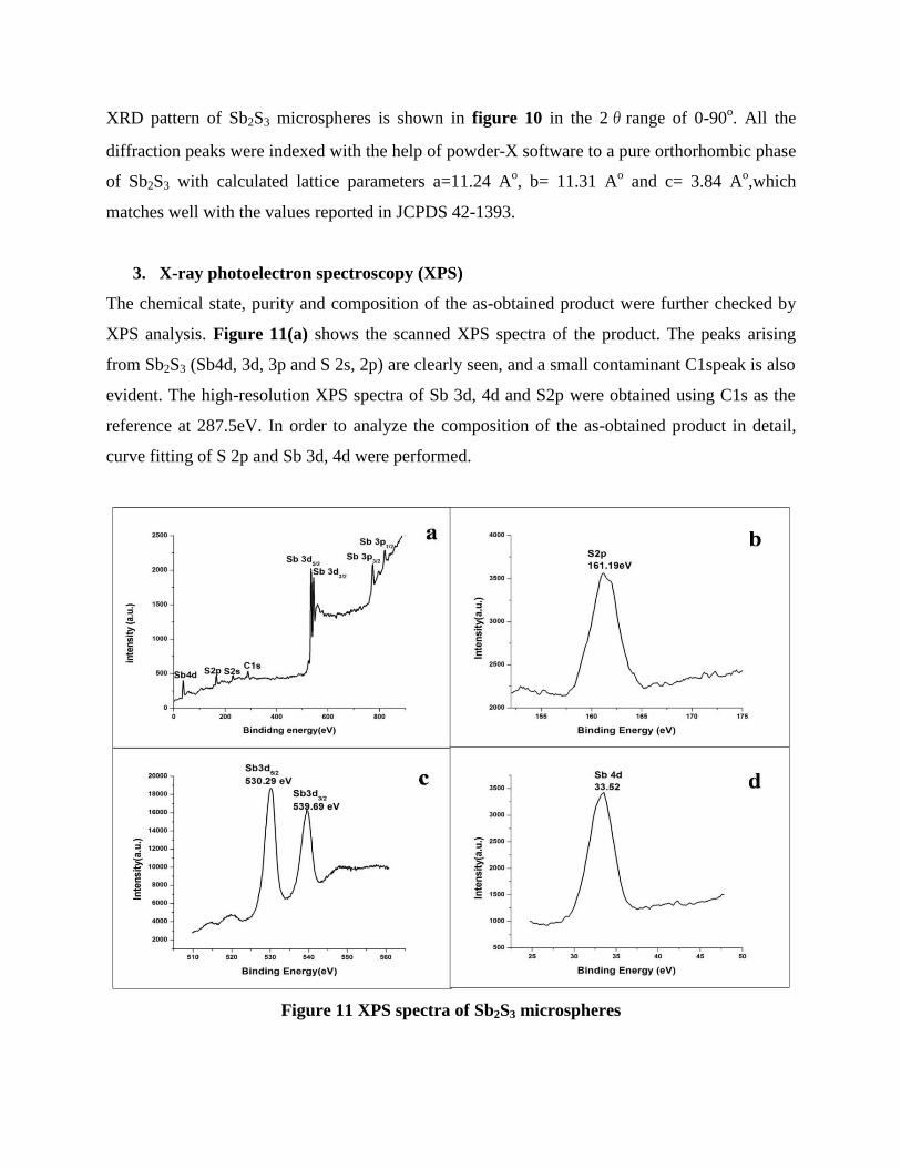
XRD pattern of Sb2S3 microspheres is shown in figure 10 in the 2θrange of 0-90o. All the
diffraction peaks were indexed with the help of powder-X software to a pure orthorhombic phase
of Sb2S3 with calculated lattice parameters a=11.24 Ao, b= 11.31 A
o and c= 3.84 A
o,which
matches well with the values reported in JCPDS 42-1393.
3. X-ray photoelectron spectroscopy (XPS)
The chemical state, purity and composition of the as-obtained product were further checked by
XPS analysis. Figure 11(a) shows the scanned XPS spectra of the product. The peaks arising
from Sb2S3 (Sb4d, 3d, 3p and S 2s, 2p) are clearly seen, and a small contaminant C1speak is also
evident. The high-resolution XPS spectra of Sb 3d, 4d and S2p were obtained using C1s as the
reference at 287.5eV. In order to analyze the composition of the as-obtained product in detail,
curve fitting of S 2p and Sb 3d, 4d were performed.
Figure 11 XPS spectra of Sb2S3 microspheres
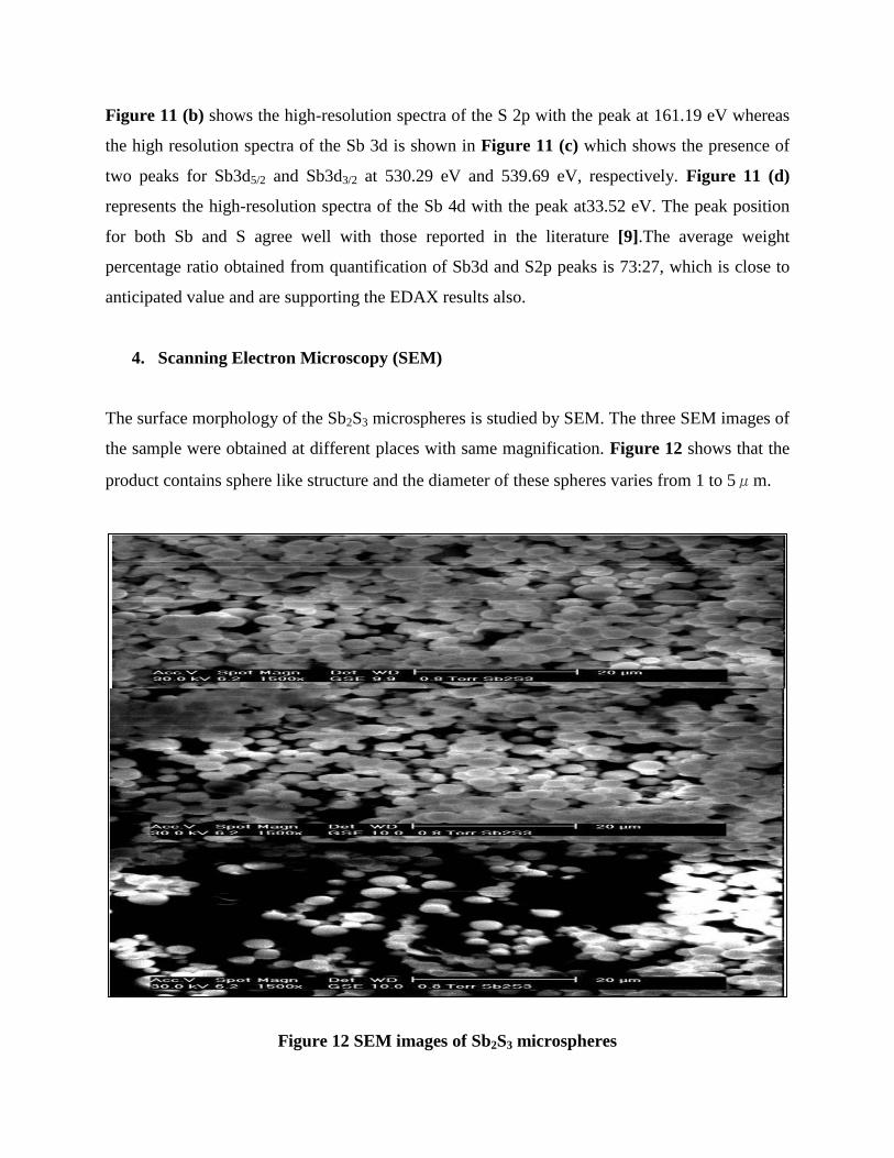
Figure 11 (b) shows the high-resolution spectra of the S 2p with the peak at 161.19 eV whereas
the high resolution spectra of the Sb 3d is shown in Figure 11 (c) which shows the presence of
two peaks for Sb3d5/2 and Sb3d3/2 at 530.29 eV and 539.69 eV, respectively. Figure 11 (d)
represents the high-resolution spectra of the Sb 4d with the peak at33.52 eV. The peak position
for both Sb and S agree well with those reported in the literature [9].The average weight
percentage ratio obtained from quantification of Sb3d and S2p peaks is 73:27, which is close to
anticipated value and are supporting the EDAX results also.
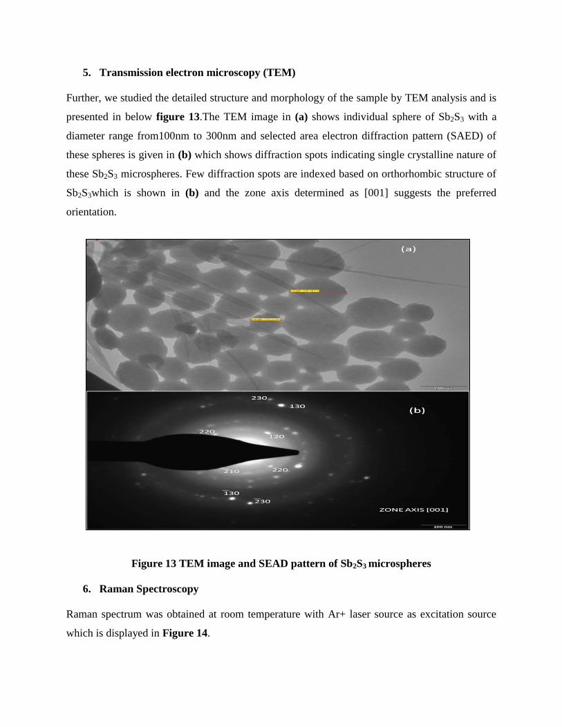
4. Scanning Electron Microscopy (SEM)
The surface morphology of the Sb2S3 microspheres is studied by SEM. The three SEM images of
the sample were obtained at different places with same magnification. Figure 12 shows that the
product contains sphere like structure and the diameter of these spheres varies from 1 to 5μm.
Figure 12 SEM images of Sb2S3 microspheres
5. Transmission electron microscopy (TEM)
Further, we studied the detailed structure and morphology of the sample by TEM analysis and is
presented in below figure 13.The TEM image in (a) shows individual sphere of Sb2S3 with a
diameter range from100nm to 300nm and selected area electron diffraction pattern (SAED) of
these spheres is given in (b) which shows diffraction spots indicating single crystalline nature of
these Sb2S3 microspheres. Few diffraction spots are indexed based on orthorhombic structure of
Sb2S3which is shown in (b) and the zone axis determined as [001] suggests the preferred
orientation.
Figure 13 TEM image and SEAD pattern of Sb2S3 microspheres
6. Raman Spectroscopy
Raman spectrum was obtained at room temperature with Ar+ laser source as excitation source
which is displayed in Figure 14.

Figure 14 Raman spectrum of the Sb2S3 microsphere
The appearance of the peaks at 151, 188, 252, 305, 372 and 450 cm-1
is in good agreement with
the reported Raman spectra. The presence of sharp peaks at 151cm-1, 188cm
-1 and 252cm
-1
suggests the formation of well crystalline products. The low intensity peak at 305 cm-1
and 372
cm-1
can be assigned to the unit SbS3 pyramid of the material having C3v symmetric mode. The
presence of a relatively broad peak at 450 cm-1
may be due to the symmetric stretching of the Sb-
S-S-Sb bond of Sb2S3, which can be accounted on the basis of existing literature [10].
7. TGA
Figure 15 TGA plot of Sb2S3 microspheres in air atmosphere
A TGA spectrum in air of the prepared Sb2S3 microspheres is shown in Figure 15 which reflects
weight loss between 178-292°C. The weight loss may be due to formation of oxide of antimony

and sulfur evaporation in this temperature range. We have used the theoretical models viz.
Broido (BR) [11], Coats Redfern (CR) [12] and Piloyan-Novikova (PN) [13] relations for
calculating the activation energy in the weight loss region of TGA curve. The calculated values
of activation energy from these relations are shown in below table 4.
Table 4 activation energy from TGA
Name of
Model Broido relation
Coats-Redfern
relation
Piloyan-Novikova
relation
Activation
energy 0.79eV 0.64eV 0.16eV
8. UV-Vis Spectroscopy
Figure 16 (αhυ)2 versus hυ curve for the Sb2S3 microspheres
Figure 16 shows (αhυ)2 – hυ graph, from which we determined the value of bandgap which
comes out to be 1.62eV which is near to optimum value for photovoltaic conversion, suggesting
that these microspheres may be suitable for applications in solar energy and optoelectronic
devices [14].
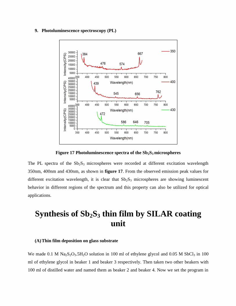
9. Photoluminescence spectroscopy (PL)
Figure 17 Photoluminescence spectra of the Sb2S3 microspheres
The PL spectra of the Sb2S3 microspheres were recorded at different excitation wavelength
350nm, 400nm and 430nm, as shown in figure 17. From the observed emission peak values for
different excitation wavelength, it is clear that Sb2S3 microspheres are showing luminescent
behavior in different regions of the spectrum and this property can also be utilized for optical
applications.
Synthesis of Sb2S3 thin film by SILAR coating
unit
(A) Thin film deposition on glass substrate
We made 0.1 M Na2S2O3.5H2O solution in 100 ml of ethylene glycol and 0.05 M SbCl3 in 100
ml of ethylene glycol in beaker 1 and beaker 3 respectively. Then taken two other beakers with
100 ml of distilled water and named them as beaker 2 and beaker 4. Now we set the program in

the SILAR unit as (a) dipping time: 10 s for beaker 1 and 3 and 5 s for beaker 2 and 4. (b) Drying
time: 10s for all the 4 beakers. This program is set for 35 cycles and we have thin film of Sb2S3
deposited on glass substrate as shown in figure 18.
Figure 18 Sb2S3 thin film on glass substrate
(B) Charecterization
1. Energy Dispersive Analysis of X-rays (EDAX)
The EDAX spectra of deposited Sb2S3 thin films on glass substrates using SILAR method with
different cycles and concentrations {cycles: 25 cycle, 30 cycle, 33cycle, 50 cycle; concentration:
0.05:0.1 M, 0.1:0.2M} are shown in figure 19 [a, b, c, d] respectively indicating the presence of
elements of S and Sb and the atomic percentage of Sb and S are shown in table 5 (a,b,c,d)
respectively.

Figure 19 EDAX spectra of Sb2S3 thin films
Table 5 (a)
Element Weight %
(calculated)
Weight %
(observed)
Atomic %
(calculated)
Atomic %
(observed)
Sb 71.68 94.26 59.02 81.21
S 28.29 5.74 41.97 18.79
Table 5 (b)
Elements Weight %
(calculated)
Weight %
(observed)
Atomic %
(calculated)
Atomic %
(observed)
Sb 71.68 94.46 59.02 81.77
S 28.29 5.54 41.97 18.23
Table 5 (c)
Elements Weight %
(calculated)
Weight %
(observed)
Atomic %
(calculated)
Atomic %
(observed)
Sb 71.68 88.46 59.02 66.88
S 28.29 11.54 41.97 30.12
a b
c d

Table 5 (d)
Elements Weight %
(calculated)
Weight %
(observed)
Atomic %
(calculated)
Atomic %
(observed)
Sb 71.68 95.59 59.02 85.11
S 28.29 4.41 41.97 14.89
2. X-ray diffraction
Figure 20 shows X-ray diffractograms of Sb2S3 thin films with different concentrations and
depositing cycles. From these diffractograms we calculated lattice parameters and crystallite size
whose values are narrated below for each film with different concentrations and depositing
cycles.
Figure 20 X-ray diffractogram of Sb2S3 thin films

The lattice parameter a = 11.23 A°, b = 11.07 A°, c = 3.81 A° and crystallite size D = 13.8 nm.
(Cycles: 25, SbCl3:0.05M, Na2O2S3 5H2O:0.1M)
The lattice parameter a = 11.11 A°, b = 11.31 A°, c = 3.85 A° and crystallite size D = 15.06 nm.
(Cycles: 30, SbCl3:0.05M, Na2S2O3 5H2O:0.1M)
The lattice parameter a = 10.78 A°, b = 11.64 A°, c = 3.85 A° and crystallite size D = 11.06 nm.
(Cycles: 33, SbCl3:0.05M, Na2S2O3 5H2O:0.1M)
The lattice parameter a = 11.74 A°, b = 11.28 A°, c = 3.66 A° and crystallite size D = 9.19 nm.
(Cycles: 50, SbCl3:0.1M, Na2O2O3 5H2O:0.2M). Calculated lattice parameters are in agreement
with the reported values (JCPDS – 42 – 1933) a = 11.23A°, b = 11.32 A°, c = 3.841 A° [15].
3. Photoluminescence spectroscopy
Room temperature PL spectra of Sb2S3 thin films, for different cycles and concentrations are
shown in figure 21.
Figure 21 PL spectra of Sb2S3 thin films at room temperature
The emission peaks presents broad bands over 430-480nm range with strong violet emission
peaks centered at same wavelengths of 460nm [2.70eV] for all thin films [16].
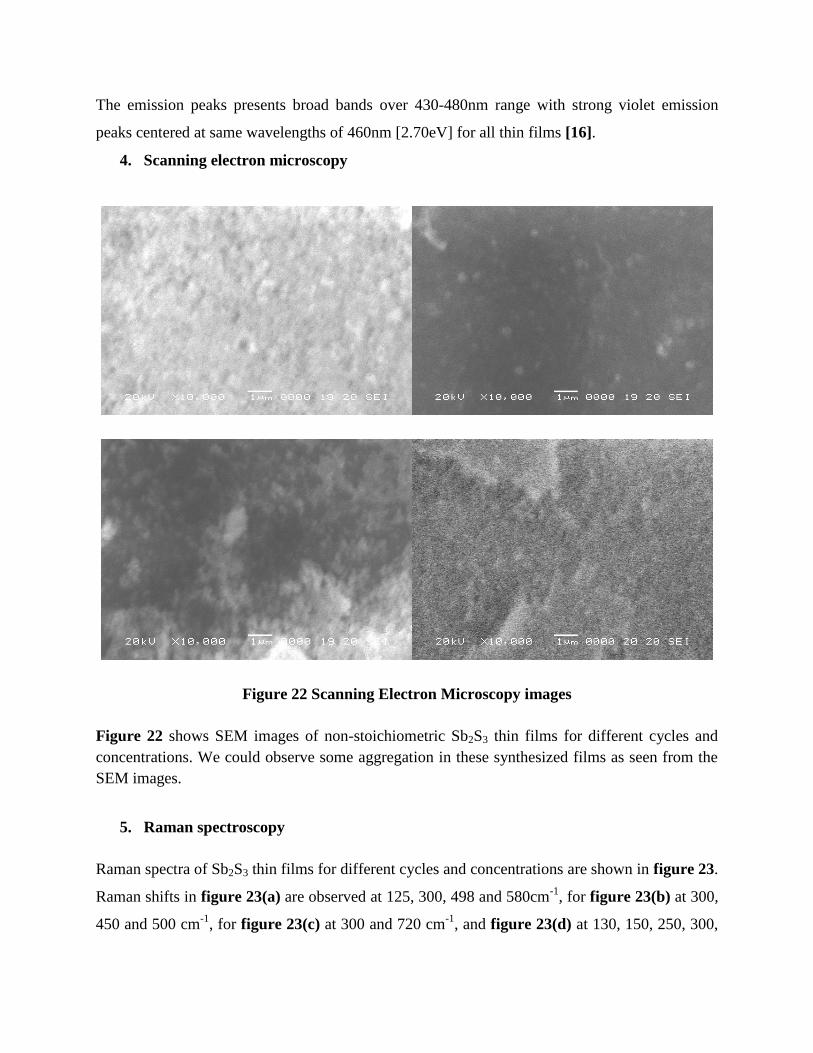
4. Scanning electron microscopy
Figure 22 Scanning Electron Microscopy images
Figure 22 shows SEM images of non-stoichiometric Sb2S3 thin films for different cycles and
concentrations. We could observe some aggregation in these synthesized films as seen from the
SEM images.
5. Raman spectroscopy
Raman spectra of Sb2S3 thin films for different cycles and concentrations are shown in figure 23.
Raman shifts in figure 23(a) are observed at 125, 300, 498 and 580cm-1
, for figure 23(b) at 300,
450 and 500 cm-1
, for figure 23(c) at 300 and 720 cm-1
, and figure 23(d) at 130, 150, 250, 300,

450, 500 and 600 cm-1
. These values of Raman shift are in agreement with the Raman spectrum
reported by Lopez et al. [7].
Figure 23 Raman spectra of Sb2S3 thin films
Bi2S3 nanorods prepared at room temperature
(A) Synthesis method for Bi2S3 nanorods
All chemicals were analytical grade and used without any further purification. In typical
synthesis, 1 ml hydrochloric acid (36Wt%) and 0.243g of bismuth nitrate (Bi(NO3)3·5H2O) were
added into 10 ml of distilled water. after stirring for 2 minute, 0.0564 g thioacetamide (TAA)
was introduced and stirring was continued (the final concentration of Bi (NO3)3 and TAA was
0.05 mol L-1
). This resulted solution was kept at room temperature for 24 h under static
condition. The solution turned transparent to brown then to black gradually and precipitates at
a b
d c

last were settled down. The resulting product was filtered, collected and washed with distilled for
several times and dried in air and shown in figure 24.
Figure 24 Bi2S3 nanorods
(A) Charectsrization
1. Energy dispersive analysis of X-ray (EDAX)
Figure 25 shows the EDAX spectra for the Bi2S3 nanostructure. The wt% and at% are stated in
table 6 given below.
Figure 25 EDAX spectra of the as obtained Bi2S3 nanostructure

Table 6 wt% and at% of the Bi2S3 nanostructure
composition Elements Wt % At %
Bi2S3 Bi 84.45 45.46
S 15.55 54.54
We can conclude from EDAX spectra that no other impurities are incorporated in the sample and
excess of Bi is observed in comparison to S which is nearly consistent with the desirable
stoichiometry of Bi2S3.
2. X-ray diffraction (XRD)
Figure 26 XRD spectra of Bi2S3 nanorods
Figure 26 shows the powder X-ray diffraction of Bi2S3 sample. X-ray powder diffraction (XRD)
analysis confirms that the as-synthesized product belongs to the orthorhombic system and

diffraction peaks are indexed with the help of powder X-software. The calculated lattice
constants are a= 11.15 Å, b=11.30Å and c = 3.98Å (space group pbnm), which are consistent
with the JCPDS no.43-1471 [17].
3. X-ray photoelectron spectroscopy (XPS)
XPS spectra shown in figure 27(a). The binding energies obtained in the XPS analysis were
corrected for specimen charging by referring the C1s line to 284.60 eV. All other peaks can be
assigned to O, Bi and S elements.
Figure 27 (a) XPS spectra of prepared Bi2S3 sample (b, c) high resolution spectra of Bi and
S regions of the prepared Bi2S3 sample
The peak at 225.29 eV corresponds to S2s as shown in figure 27(b) whereas the two strong peaks
at 159.3 and 164.5 eV in figure 27(c) are assigned to Bi4f7/2 and Bi4f5/2 respectively, with a
typical Bi4f spin-orbit doublet splitting of 5.2eV, which is consistent with the reported values
[18].
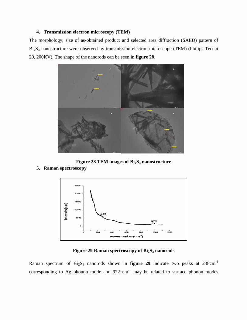
4. Transmission electron microscopy (TEM)
The morphology, size of as-obtained product and selected area diffraction (SAED) pattern of
Bi2S3 nanostructure were observed by transmission electron microscope (TEM) (Philips Tecnai
20, 200KV). The shape of the nanorods can be seen in figure 28.
Figure 28 TEM images of Bi2S3 nanostructure
5. Raman spectroscopy
Figure 29 Raman spectroscopy of Bi2S3 nanorods
Raman spectrum of Bi2S3 nanorods shown in figure 29 indicate two peaks at 238cm-1
corresponding to Ag phonon mode and 972 cm-1
may be related to surface phonon modes
(a)
(b)
(c)
(d)

because of the high surface-to-volume ratio, which is in good agreement with values for
commercial Bi2S3 as well as the nanoparticles [19].
6. UV-vis spectroscopy
UV–vis absorption spectrum in figure 30 shows a broad absorption peak at 262nm
corresponding to the bandgap of 2.74eVwhich shows the size effect and blue shift in wavelength
in comparison to bulk material [20] which is quite similar to that synthesized by a photochemical
synthesis method.
Figure 30 UV-Vis spectra of Bi2S3 nanorods
7. Thermal gravimetric analysis (TGA)
Figure 31 shows the TGA plot of Bi2S3 as-synthesized nanorods. It shows that the weight of the
material continuously decreases with temperature. We have used the Broido relation for analysis
of TGA spectra for calculating the activation energy in the entire weight loss region. The
activation energy comes out to be 0.38 eV.
Figure 31 TGA plot for the Bi2S3 nanorods

REFERENCES
1. Powder Diffract. File, JCPDS-ICDD, 12 Campus Boulevard
Newtown Square, PA 19073-3273, U.S.A., 2001.
2. A. M. Morales, C. M. Lieber,
Science, 279 (1998) 208.
3. G. Q. Zhu, P. Liu, H. Y. Miao, J. P. Zhu, X. B. Bian, Y. Liu, B. Chen,X. B. Wang,
Mat. Res. Bull., 43 (2008) 2636.
4. B. D. Cullity,
Elements of X-rays Diffraction (2nd
edition), 102 (Addison-Wesley1978)
5. J. Ota, P. Roy, S. Srivastava, B. Nayak, A. Saxena,
Cryst.Growth Des.8 (2008) 2019.
6. M. A. El IdrissiRaghni, B. Bonnet, M. L. Hafid, J. O. Fourcade, J. C.Jumas,
J. Alloys Compd., 260 (1997) 7.
7. B. H. Juarez, S. Rubio, C. Lopez,
Adv. Mater. 14 (2002) 1486.
8. G. Ilinca, R. Caracas,
Raman and Infrared spectra of stibnite, Sb2S3, American GeophysicalUnion, Tall
meeting-2006.
9. J. Ota, J. Chen, X. Yang, L. Lu, X. Wang,
J PhysChem C, 111 (2007) 14072.
10. C. An, K. Tang, Q. Yang, Y. Qian,
Inorg. Chem., 42 (2003) 8081.
11. A. Broido,
J. Polym. Sci., Part B, 7 (1969) 1761
12. A. W. coats and J. P. Redfern,
Nature, 201(1964) 68
13. G. O. Piloyan and O. S. Novikova
Russian J. Inorg. Chem., 12 (1966) 313
14. Y. Yu, R. H. Wang, Q. Chen, L.M. Peng
J. Phys. Chem. B, 109 (2005) 23312.

15. Zhu, P. Lio, H.Y. Miao, J. P. Zhu, X. B. Bina, Y Liu, B Chen, X. B. Wang
Materials research bulletin. 43 (2008) 2636-2642.
16. J. Kavinchan, T. Thongtem, S. Thongte
Chalcogenide Letters, 9 (2012) 365-370.
17. H. C. Liao, M. C. Wu, M. H. Jao, C. M. Chuang, Y. F. Chen, W. F. Su
Cry. Engg. Com. (2012) DOI: 10.1039/c2ce06154f.
18. Y. Zhao, Y. Xie, J. S. Jie, C. Y. Wu, S. Yan
J. Mat. Chem., 19 (2009) 3378.
19. O. Rabin, J. M. Perez, J. Grimm, G. Wojtikewicz, R. Weissleder
Nat. Mater., 17 (2005) 6094.
20. R. Vogel, P. Hoyer, H. Weller
J. Phys. Chem., 98 (12) (1994) 3183.

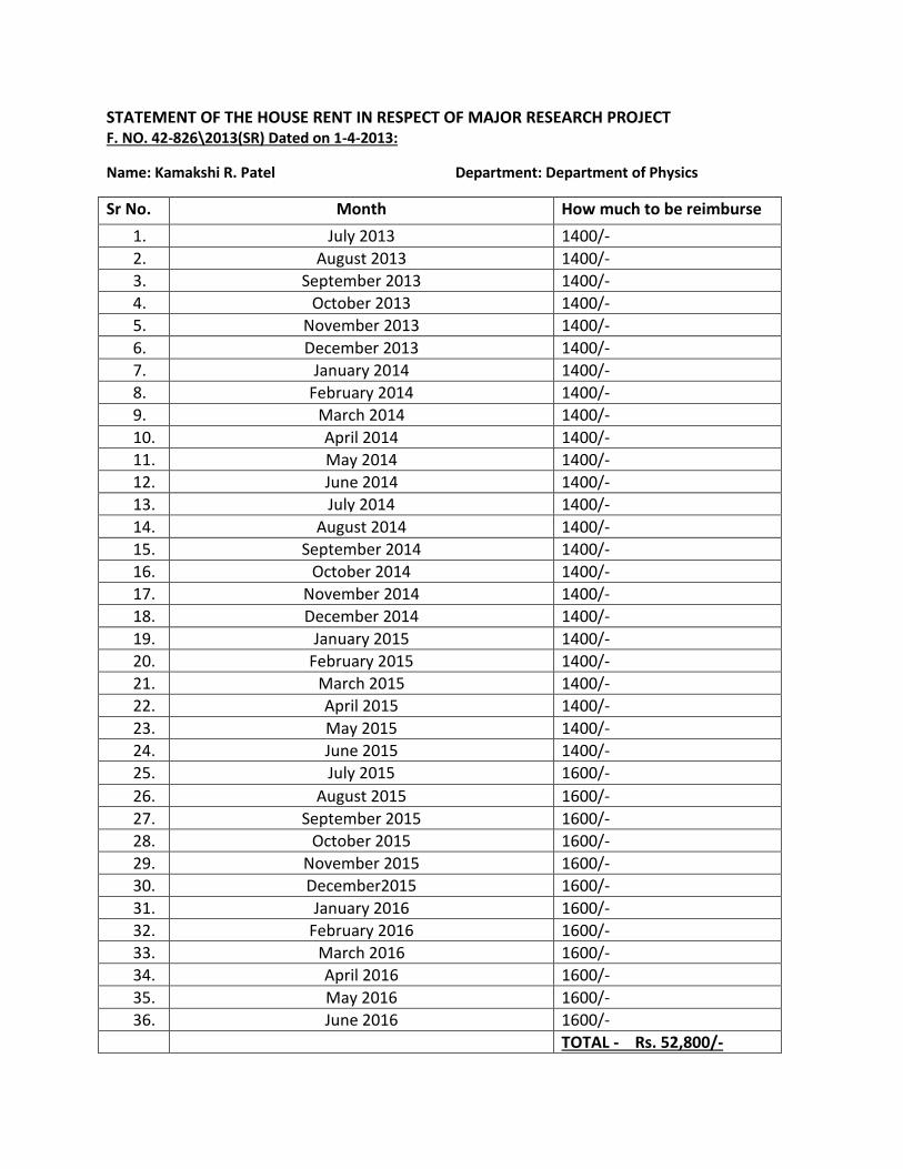
STATEMENT OF THE HOUSE RENT IN RESPECT OF MAJOR RESEARCH PROJECT F. NO. 42-826\2013(SR) Dated on 1-4-2013:
Name: Kamakshi R. Patel Department: Department of Physics
Sr No. Month How much to be reimburse
1. July 2013 1400/-
2. August 2013 1400/-
3. September 2013 1400/-
4. October 2013 1400/-
5. November 2013 1400/-
6. December 2013 1400/-
7. January 2014 1400/-
8. February 2014 1400/-
9. March 2014 1400/-
10. April 2014 1400/-
11. May 2014 1400/-
12. June 2014 1400/-
13. July 2014 1400/-
14. August 2014 1400/-
15. September 2014 1400/-
16. October 2014 1400/-
17. November 2014 1400/-
18. December 2014 1400/-
19. January 2015 1400/-
20. February 2015 1400/-
21. March 2015 1400/-
22. April 2015 1400/-
23. May 2015 1400/-
24. June 2015 1400/-
25. July 2015 1600/-
26. August 2015 1600/-
27. September 2015 1600/-
28. October 2015 1600/-
29. November 2015 1600/-
30. December2015 1600/-
31. January 2016 1600/-
32. February 2016 1600/-
33. March 2016 1600/-
34. April 2016 1600/-
35. May 2016 1600/-
36. June 2016 1600/-
TOTAL - Rs. 52,800/-

Annexure – IX
P. G. Department of Physics
Sardar Patel University
Vallabh Vidyanagar- 388120
PROFORMA FOR SUBMISSION OF INFORMATION AT THE TIME OF SENDING
THE FINAL REPORT OF THE WORK DONE ON THE PROJECT
1. Title of the Project: Synthesis and characterization of V2-VI3 compound in single
crystal/nanomaterial/thin film forms 2. NAME AND ADDRESS OF THE PRINCIPAL INVESTIGATOR: Prof. M. P. Deshpande
Department of Physics, Sardar Patel University
Anand, Gujarat 3. NAME AND ADDRESS OF THE INSTITUTION: Department of Physics, Sardar Patel
University, Vallabh Vidyanagr, Anand, Gujarat
4. UGC APPROVAL LETTER NO. AND DATE: F.No. 42-826/2013 (SR) dated 22nd
March
2013. 5. DATE OF IMPLEMENTATION: 1
st April 2013
6. TENURE OF THE PROJECT: 4 years
7. TOTAL GRANT ALLOCATED: Rs. 11, 16,800
8. TOTAL GRANT RECEIVED: Rs. 10, 08,300
9. FINAL EXPENDITURE: Rs. 10, 25,096
10. TITLE OF THE PROJECT: Synthesis and characterization of V2-VI3 compound in single
crystal/nanomaterial/thin film forms 11. OBJECTIVES OF THE PROJECT:
a. Synthesis and characterization of V2-VI3 compound in single crystal/ nanomaterials/ thin
film forms.
b. Characterization of synthesized material structurally, optically, and thermally by various
techniques.
12. WHETHER OBJECTIVES WERE ACHIEVED: Yes
(GIVE DETAILS)
We undertook the preparation of single crystal of Sb2S3 by chemical vapor transport technique,
microsphere of Sb2S3 by solvothermal method, Sb2S3 thin film by SILAR coating unit and
Bi2S3 nanorods prepared at room temperature and studied their various properties by different
charactrization techniques successfully.
. The equipment sanctioned in the mentioned project, SILAR controller and Bridgman
mechanical set up are purchased from Holmarc Opto-Mechatronics (P) Ltd. Instruments, Kochi,
Kerala and Vi Micro Systems Pvt .Ltd. Perungudi, Chennai respectively are installed and
working satisfactorily. The project fellow has been trained accordingly to the requirement of
project.
13. ACHIEVEMENTS FROM THE PROJECT:
Single crystals of Sb2S3 , Microspheres of Sb2S3 , Sb2S3 thin film by SILAR coating unit and Bi2S3
nanorods were successfully prepared and characteristed by different techniques available in the
department and other nearby institutes. Single crystals of Sb2S3 grown by vapour phase technique has
not been seen reported so far in the literature.
14. SUMMARY OF THE FINDINGS ……………………………………..
(IN 500 WORDS)
Single crystals of Sb2S3 were prepared in the dual zone furnace at temperature 500°C to 450°C
of the source zone and growth zone respectively. The grown single crystals of Sb2S3 were in the
form of needle shape.The composition of the grown crystals were determined from EDAX
spectra. X-ray diffraction pattern of Sb2S3 powder (polycrystalline) were indexed with the help
of powder-X software to pure orthorhombic phase of Sb2S3 with calculated lattice parameters: a
= 11.239 Ao, b = 11.313 A
o and c = 3.841 A
o. The surface morphology of grown single crystals
of Sb2S3 at different magnification of 100X, 50X and 500X using SEM showed that crystals
surfaces are possessing cracks and visible inclusions. The Raman spectrum of Sb2S3 single
crystal at room temperature using Ar laser source exhibits seven resonant peaks at about 115,
147, 190, 252, 282, 300 and 373 cm-1
in the range of 100 - 400 cm-1
. The presence of sharp peaks
at 190 and 252cm-1
suggests the formation of well crystalline product. The TGA curve of Sb2S3
crystal under nitrogen (N2) atmosphere showed that Sb2S3 decomposes slowly from 27°C to
472°C having small weight loss of nearly 2%.
Microspheres of Sb2S3 were prepared using solvothermal method.The elemental compositions
of Sb2S3 microspheres synthesized indicated no impurity content in it. XRD pattern of Sb2S3
microspheres were indexed with the help of powder-X software to a pure orthorhombic phase of
Sb2S3 with calculated lattice parameters a=11.24 Ao, b= 11.31 A
o and c= 3.84 A
o,which matches
well with the values reported in JCPDS 42-1393.The chemical state, purity and composition of
the as-obtained product were further checked by XPS analysis. The peaks arising from Sb2S3
(Sb4d, 3d, 3p and S 2s, 2p) were clearly seen, and a small contaminant C1s peak is also evident.
The high-resolution XPS spectra of Sb 3d, 4d and S2p were obtained using C1s as the reference
at 287.5eV.The surface morphology of the Sb2S3 microspheres is studied by SEM showing
spheres from 1 to 5μm and TEM analysis showed range from100nm to 300nm. The selected
area electron diffraction pattern (SAED) of these spheres indicated single crystalline nature of
these Sb2S3 microspheres. Raman spectrum was obtained at room temperature with Ar+ laser
source as excitation source .The appearance of the peaks at 151, 188, 252, 305, 372 and 450 cm-1
is in good agreement with the reported Raman spectra. TGA spectrum in air of the prepared
Sb2S3 microspheres reflects weight loss between 178-292°C.The value of bandgap which comes
out to be 1.62eV which is near to optimum value for photovoltaic conversion, suggesting that
these microspheres may be suitable for applications in solar energy and optoelectronic devices.
From the observed emission peak values for different excitation wavelength, it is clear that Sb2S3
microspheres are showing luminescent behavior in different regions of the spectrum and this
property can also be utilized for optical applications.
Sb2S3 thin film were synthesized by by SILAR coating unit purchased in this project.The EDAX
spectra of deposited Sb2S3 thin films on glass substrates using SILAR method with different
cycles and concentrations {cycles: 25 cycle, 30 cycle, 33cycle, 50 cycle; concentration: 0.05:0.1
M, 0.1:0.2M} indicated the presence of elements of S and Sb. X-ray diffractograms of Sb2S3 thin
films with different concentrations and depositing cycles were recorded and we calculated lattice
parameters which were in agreement with the reported values (JCPDS – 42 – 1933) a = 11.23A°,
b = 11.32 A°, c = 3.841 A°. Room temperature PL spectra of Sb2S3 thin films, for different
cycles and concentrations showed the emission peaks presents broad bands over 430-480nm
range with strong violet emission peaks centered at same wavelengths of 460nm [2.70eV] for all
thin films. We could observe some aggregation in these synthesized films as seen from the SEM
images. Raman spectra of Sb2S3 thin films for different cycles and concentrations showed Raman
shifts which were in agreement with the Raman spectrum reported.
Bi2S3 nanorods were prepared at room temperature by chemical route.We can conclude from EDAX
spectra that no other impurities are incorporated in the sample and excess of Bi is observed in
comparison to S which is nearly consistent with the desirable stoichiometry of Bi2S3.
The powder X-ray diffraction of Bi2S3 sample. X-ray powder diffraction (XRD) analysis
confirms that the as-synthesized product belongs to the orthorhombic system and diffraction
peaks are indexed with the help of powder X-software. The calculated lattice constants are a=
11.15 Å, b=11.30Å and c = 3.98Å (space group pbnm), which are consistent with the JCPDS
no.43-1471.The binding energies obtained in the XPS analysis were corrected for specimen
charging by referring the C1s line to 284.60 eV. All other peaks can be assigned to O, Bi and S
elements.The peak at 225.29 eV corresponds to S2s whereas the two strong peaks at 159.3 and
164.5 eV in are assigned to Bi4f7/2 and Bi4f5/2 respectively, with a typical Bi4f spin-orbit doublet
splitting of 5.2eV, which is consistent with the reported values.The morphology, size of as-
obtained product and selected area diffraction (SAED) pattern of Bi2S3 nanostructure were
observed by transmission electron microscope (TEM) (Philips Tecnai 20, 200KV). Raman
spectrum of Bi2S3 nanorods indicated two peaks at 238cm-1
corresponding to Ag phonon mode
and 972 cm-1
may be related to surface phonon modes because of the high surface-to-volume
ratio, which is in good agreement with values for commercial Bi2S3 as well as the
nanoparticles.UV–vis absorption spectrum showed a broad absorption peak at 262nm
corresponding to the bandgap of 2.74eVwhich shows the size effect and blue shift in wavelength
in comparison to bulk material .The TGA plot of Bi2S3 as-synthesized nanorods. It shows that
the weight of the material continuously decreases with temperature.
15. CONTRIBUTION TO THE SOCIETY ……………………………….
(GIVE DETAILS)
For industrial applications, the most important question is the product’s price in relation to its
properties. In most cases, single crystals/thin films/nanomaterials of different materials and
products utilizing this form are significantly more expensive than conventional products. In the
case of single crystals/thin films/nanomaterials the increase in price is sometimes more
pronounced than improvement in properties, and therefore economically interesting applications
of them are often found only in areas where specific properties are demanded that are beyond the
reach of conventional materials. Hence, as long as the use of single crystals/thin
films/nanomaterials with new properties provide the solution to a problem which cannot be
solved with conventional materials, the price becomes much less important. Finally, only those
materials which exhibit new properties leading to novel applications, beyond the reach of
conventional materials, promise interesting results.
Scanned by CamScanner

Copyright © 2014 American Scientific PublishersAll rights reservedPrinted in the United States of America
R E S E A R CH AR T I C L E
Advanced Science LettersVol. 20, 1102–1106, 2014
Sb2S3 Microspheres Prepared by
Solvothermal Method
M. P. Deshpande1, Pallavi Sakariya1�2�∗, Sandip V. Bhatt1,Kamakshi R. Patel1, Nikita H. Patel1, and S. H. Chaki1
1Department of Physics, Sardar Patel University, Vallabh Vidyanagar 388120, Gujarat, India2Babaria Institute of Technology, NH-8, Varnama, Vadodara 391240, Gujarat, India
We report here synthesis of Sb2S3 microsphere via solvothermal method using SbCl3 (Antimony chloride) andsulfur powder as a starting materials and N,N-dimethylformamide (DMF) as solvent. Energy dispersive analy-sis of X-rays (EDAX) and X-ray diffraction (XRD) studies indicated that the prepared microspheres are nearlystoichiometry in composition and corresponds to pure orthorhombic phase of Sb2S3. The purity and composi-tion of obtained product was further confirmed by X-ray photoelectron spectroscopy (XPS). Scanning electronmicroscopy (SEM) and transmission electron microscopy (TEM) studies show the sphere like structure of Sb2S3
particles with diameter ranging between 100 nm to 300 nm. Optical absorption experiment has shown that Sb2S3
microspheres are semiconductor with a bandwidth Eg ≈ 1�62 eV, near to the optimum value for photovoltaic con-version, suggesting that Sb2S3 microspheres could be used in solar energy and optoelectronic application. Wefurther studied thermal properties of Sb2S3 microspheres in powder form by thermogravimetric analysis (TGA)in air atmosphere which reflects that these microspheres are stable upto 200 �C. Photoluminesence studies aredone on this sample which shows its luminesence behaviour. Raman spectra at room temperature has beenused to study various phonon modes in Sb2S3 microspheres.
Keywords:
1. INTRODUCTIONV–VI group binary chalcogenides (AV
2 BVI3 ; A = As, Sb, Bi ; B =
S, Se, Te) have atrracted much attention due to their good pho-
tovoltaic properties and high thermoelectric power, which allow
potential applications in optical, electronic and thermoelectric
cooling devices.1 Binary chalcogenides compound have received
attention recently because of their potential for optical storage.2
Antimony sulfide (Sb2S3) (stibnite) is a direct band gap and
highly anisotropic V–VI group binary chalcogenide semicon-
ductor with a layered structure parallel to growth direction
and crystallizes in an orthorhombic phase well known for its
high photosensitivity and high thermoelectric properties.3 Anti-
mony sulfide (Sb2S3) has been extensively studied due to its
device applications in photoconducting targets of television cam-
eras, electronic devices, optoelectronics devices and infrared
spectroscopy.4�5
One important function of Sb2S3 is that it can be used as
the starting material for synthesizing other related compounds.6�7
It has also been used in thermoelectric cooling technologies and
optoelectronics in the IR region.5�8
∗Author to whom correspondence should be addressed.
The literature survey shows that several morphologies of
antimony trisulfide (stibnite) have been fabricated including
nanoparticles,9 nanorods,10–12 nanowhiskers,13 microtubular,14�15
and microspheres16 by various methods. But a very few work-
ers have prepared the microspheres via solvothermal method.
Here in we prepared Sb2S3 microspheres using SbCl3 (Antimony
chloride) and sulfur powder as a starting material. The struc-
tural, optical and thermal properties of the prepared Sb2S3 micro-
spheres were studied and the results obtained are discussed in
detail in this paper.
2. EXPERIMENTAL PROCEDUREAll of the chemical reagents used in this experiment were of
analytical grade and were used without further purification. In a
typical procedure, 0.23 g antimony chloride (SbCl3) and 0.45 g
tartaric acid were dissolved in 16 mL N ,N -dimethylformamide
(DMF). In this solution about 0.244 g sulfur powder was added
with stirring. This mixed solution was transfered into a teflon-
lined stainless steel autoclave. The autoclave was sealed and
maintained at 120 �C for 4 h and then cooled to room temperature
naturally. The precipitates were collected and washed with dis-
tilled water for several times. Then, the precipitates were dried in
1102 Adv. Sci. Lett. Vol. 20, No. 5/6, 2014 1936-6612/2014/20/1102/005 doi:10.1166/asl.2014.5498

R E S E A R CH AR T I C L EAdv. Sci. Lett. 20, 1102–1106, 2014
Fig. 1. EDAX spectra of Sb2S3.
air. Finally, the resultant burgundy colored powder sample were
obtained and characterized by various techniques.
3. CHARACTERIZATION TECHNIQUESThe as prepared sample was characterized by X-ray powder
diffraction (XRD) on a X-ray diffractrometer (Philips Xpert
MPD) with Cu-K� radiation �� = 1�54 � to study struc-
tural properties and the chemical composition of the prepared
sample was analyzed by energy dispersive analysis of X-ray
(EDAX) (Philips EM 400 electron microscope). XPS measure-
ments were performed for confirmation of EDAX results on a
ESCA lab X-ray photoelectron spectrometer with an excitation
source of AlK�= 1486�6 eV. The surface morphology was stud-
ied by using scanning electron microscopy (SEM) (Model-XL
30 ESEM) and transmission electron microscope (TEM) (Philips
Tecnai 20, 200 KV). The Raman scattering experiments were car-
ried out at room temperature under the backscattering geometry
using Jobin-Yvon Horiba labram, HR800 single monochromatic
coupled with “peltier cooled” charged coupled device (CCD)
and 488 nm line of an Argon (Ar+) laser was used for excita-
tion. Absorption spectra in UV-VIS range for prepared sample
was carried at room temperature using UV-VIS-NIR spectrom-
eter (Perkin Elmer). A Photoluminessence (PL) spectrum was
obtained by Fluoromax-Compact spectrometer with Xe lamp at
room temperature. We also studied thermogravimetric analysis
(TGA) on the sample in the range between room temperature to
500 �C in air atmosphere.
4. RESULTS AND DISCUSSIONFigure 1 shows the EDAX spectra of prepared Sb2S3 micro-
spheres suggesting that the sample contain only antimony and
sulfur elements. Table I provides the elemental composition in
terms of weight percentage of elements obtained from EDAX
result reveal the desirable stoichiometry of Sb2S3.
Table I. Elemental composition of Sb2S3 microspheres.
Composition Wt% of present element in Sb2S3
Sb2S3 Sb S71.08 28.92
Fig. 2. The powder XRD pattern of the prepared Sb2S3 microspheres.
XRD pattern of Sb2S3 microspheres is shown in Figure 2
in the 2� range of 0–90�. All the obtained diffraction peaks
were indexed with the help of powder-X software to a pure
orthorhombic phase of Sb2S3 with calculated lattice parameters
a= 11�24 Å, b = 11�31 Å and c = 3�84 Å, which matches well
with the values reported in JCPDS 42-1393.
The chemical state, purity and composition of the as-obtained
product was further checked by XPS analysis. Figure 3(a) shows
the scanned XPS spectra of the product. The peaks arising from
Sb2S3 (Sb 4d, 3d, 3p and S 2s, 2p) are clearly seen, and a small
contaminant C1s peak is also evident. The high-resolution XPS
spectra of Sb 3d, 4d and S 2p were obtained using C1s as the
reference at 287.5 eV. In order to analyze the composition of the
as-obtained product in detail, curve fitting of S 2p and Sb 3d, 4d
were performed. Figure 3(b) shows the high-resolution spectra of
the S 2p with the peak at 161.19 eV whereas the high resolution
spectra of the Sb 3d is shown in Figure 3(c) which shows the
presence of two peaks for Sb 3d5/2 and Sb 3d3/2 at 530.29 eV
and 539.69 eV, respectively. Figure 3(d) represents the high-
resolution spectra of the Sb 4d with the peak at 33.52 eV. The
peak position for both Sb and S agree well with those reported
in the literature.17 The average weight percentage ratio obtained
from quantification of Sb3d and S2p peaks is 73:27, which is
close to anticipated value.
The surface morphology of the Sb2S3 microspheres was deter-
mined by SEM. The three SEM images of the sample were
obtained at different places with same magnification. Figure 4
shows that the product contains a large quantity of sphere like
structure without any visible by products, suggesting that the
product is of good quality. The diameter of these spheres varies
from 1 to 5 �m.
The detailed structure and morphology of the sample were
studied by TEM analysis and is presented in Figure 5. The TEM
image in Figure 5(a) shows individual sphere of Sb2S3 with
a diameter range from 100 nm to 300 nm and selected area
electron diffraction pattern (SAED) of these spheres is given in
Figure 5(b) which shows diffraction spots indicating single crys-
talline nature of these Sb2S3 microspheres. This diffraction spots
are indexed based on orthorhombic structure of Sb2S3, which is
shown in Figure 5(b) and we also determined the zone axis as
[001] suggesting the preferred orientation.
1103
R E S E A R CH AR T I C L E Adv. Sci. Lett. 20, 1102–1106, 2014
(a)
(b)
(c)
(d)
Fig. 3. (a) XPS pattern of survey scan of the as obtained product Sb2S3
microspheres (b) high resolution S 2p region (c) high resolution Sb 3d region(d) high resolution Sb 4d region.
Fig. 4. SEM images of Sb2S3 microspheres.
Raman spectra was obtained at room temperature with
Ar+ laser source as excitation source which is displayed in
Figure 6. The appearance of the peaks at 151, 188, 252, 305,
372 and 450 cm−1 is in good agreement with the reported
Raman spectrum.18 The presence of sharp peaks at 151 cm−1,
188 cm−1 and 252 cm−1 suggests the formation of well crystalline
products.19 The low intensity peak at 305 cm−1 and 372 cm−1
can be assigned to the unit SbS3 pyramid of the material hav-
ing C3v symmetric mode.20 The presence of a relatively broad
peak at 450 cm−1 may be due to the symmetric stretching of the
Sb-S-S-Sb bond of Sb2S3, which can be accounted on the basis
of existing literature.21
A TGA spectrum in air of the prepared Sb2S3 microspheres
is shown in Figure 7 which reflects weight loss between
178–292 �C. The weight loss may be due to formation of oxide
of antimony and sulfur evaporation in this temperature range.
We have used the theoretical model viz. Broido (BR) relation,22
for calculating the activation energy in the weight loss region of
1104

R E S E A R CH AR T I C L EAdv. Sci. Lett. 20, 1102–1106, 2014
Fig. 5. (a) TEM images of Sb2S3 microspheres (b) SAED pattern of theSb2S3 microspheres.
TGA curve. The corresponding plot of BR model is shown in
Figure 8. The calculated value of activation energy from broido
relations is shown in Table II.
Since Sb2S3 is important from the optoelectronic application
point of view and hence its band gap determination is carried
out using UV-Vis absorption spectra. The direct band gap energy
(Eg) for the sample is determined by fitting the absorption data
to the direct transition equation (�h�2 = A(h-Eg), where � is
the optical absorption coefficient, h is the corresponding photon
energy, Eg is the direct band gap energy of the semiconductor
and A is a constant.23 The plot (�h�2 versus h is shown in
Figure 9. The band gap is given by extrapolating the linear part
Fig. 6. Raman spectrum of the Sb2S3 microsphere.
Fig. 7. TGA plot of Sb2S3 microspheres.
Fig. 8. Plot of BR model of TGA in the weight loss region.
of the curve (�h�2 with respect to h on the x-axis and is
found to be 1.62 eV which is comparable with the reported val-
ues. This value of the band gap energy for Sb2S3 microsphere
is near the optimum value for photovoltaic conversion, suggest-
ing that Sb2S3 microspheres may be suitable for applications in
solar energy and optoelectronics.24�25 It is also noted that these
microspheres do not show quantum confinement effect, a fact
also established by these workers. This may be attributed to the
lower Bohr’s radius of this material.
Luminescence spectra is important for evaluating the optical
nature of the materials. The PL spectra of the Sb2S3 microspheres
were recorded at different excitation wavelength 350, 400 and
430 nm, as shown in Figure 10. The observed emission peak
values for different excitation wavelength are given in Table III.
Table II. Calculated values of activation energy (eV) obtained from BR
relation, PN relation and CR relation.
Name of model Broido relation
Activation energy 0.79 eV
1105
R E S E A R CH AR T I C L E Adv. Sci. Lett. 20, 1102–1106, 2014
Fig. 9. (�h�2 versus h curve for the Sb2S3 microspheres.
Fig. 10. Photoluminescence spectra of the Sb2S3 microspheres.
Table III. emission peak values at three-excitation wavelength.
Excitationwavelength (nm) Peak 1 Peak 2 Peak 3 Peak 4
350 384 V (3.23) 476 B (2.61) 574 Y (2.16) 667 R (1.86)400 439 V (2.83) 545 G (2.27) 656 R (1.89) 762 R (1.63)430 472 B (2.63) 586 Y (2.12) 646 R (1.92) 705 R (1.76)
From results shown in Table III and Figure 10. It is clear
that Sb2S3 microspheres are showing luminescent behavior in
different regions of the spectrum and probably this property can
be utilized for its further applications.
5. CONCLUSIONSb2S3 microspheres were successfully synthesized by solvother-
mal method using SbCl3 and sulfur as raw materials. Sb2S3
microspheres of desired stoichiometry are obtained as shown in
EDAX results. XRD shows that Sb2S3 microspheres belong to
pure orthorhombic phase (JCPDS 42-1393). The phase purity of
the microspheres was also confirmed by XPS. SEM and TEM
images show that Sb2S3 particles are spherical in shape hav-
ing diameter in micrometer range and spot diffraction pattern of
Sb2S3 microsphere indicating single crystalline nature of micro-
spheres. The band gap of the microspheres is found to be 1.62 eV,
which suggests that Sb2S3 microspheres can be used for applica-
tion in solar energy and optoelectronic applications. Room tem-
perature PL studies with different excitation wavelength suggests
that Sb2S3 microspheres are showing luminescence behavior in
different parts of the spectrum.
Acknowledgment: The authors are thankful to UGC, New
Delhi for providing financial support by allocating DRS/SAP
programme to the department. The authors are also grateful to
UGC—DAE Consortium for Scientific Research, Indore for pro-
viding us the facility to carry out the XPS and Raman spectra of
our sample. We would like to acknowledge SICART for assisting
us in EDAX, XRD, SEM, TEM and UV-Vis analysis.
References and Notes1. K. Y. Rajpure, C. D. Lokhande, and C. H. Bhosale, Mater. Res. Bull. 34, 79
(1999).2. K. Schwartz, The Physics of Optical Recording, Springer-Verlag (1993).3. I. H. Kim, Mater. Lett. 43, 221 (2000).4. D. Arivuoli, F. D. Gnanam, and P. Ramasamy, J. Mater. Sci. Lett. 7, 711
(1988).5. N. Kh. Anrikoson, V. F. Bankina, L. V. Poretakaya, L. E. Shelimova, and
E. V. Skudnova, Semiconducting II–VI and V–VI Compounds, edited by A.Tybulewicz, Plenum Press, New York (1969), p. 186.
6. H. O. Stephen and M. G. Kanatzidis, Inorg Chem. 36, 6050 (1997).7. A. V. Powell, S. Boissiere, and A. M. Chippindale, Chem. Mater. 12, 182
(2000).8. J. D. Smith, Arsenic, Antimony, and Bismuth, Comprehensive Inorganic Chem-
istry, Pergamon Press, Oxford (1973), Vol. 2, p. 547.9. S. H. Yu, L. Shu, Y. S. Wu, Y.T. Qian, Y. Xie, and L. Yang, Mater. Res. Bull.
33, 1207 (1998).10. J. Yang, J. H. Zeng, S. H. Yu, L. Yang, Y. H. Zhang, and Y. T. Qian, Chem.
Mater. 12, 2924 (2000).11. C. Li, X. G. Yang, Y. F. Liu, Z. Y. Zhao, and Y. T. Qian, J. Cryst. Growth
255, 342 (2003).12. M. S. Mo, Z. Y. Zhu, X. G. Yang, X. Y. Liu, S. Y. Zhang, J. Gao, and Y. T. Qian,
J. Cryst. Growth 256, 377 (2003).13. H. Wang, J. J. Zhu, and H. Y. Chen, Chem. Lett. 12, 1242 (2002).14. X. W. Zheng, Y. Xie, L. Y. Zhu, X. C. Jiang, Y. B. Jia, W. H. Song, and Y. P.
Sun, Inorg. Chem. 41, 455 (2002).15. Q. Yang, K. B. Tang, C. R. Wang, Y. T. Qian, W. C. Yu, G. E. Zhou, and F. Q.
Li, J. Mater. Chem. 11, 257 (2001).16. B. Cheng and E. T. Samulski, Mater. Res. Bull. 38, 297 (2003).17. J. Ota, J. Chen, X. Yang, L. Lu, and X. Wang, J. Phys. Chem. C 111, 14072
(2007).18. B. H. Juarez, S. Rubio, and C. Lopez, Adv. Mater. 14, 1486 (2002).19. Jyotiranjan Ota, Poulomi Roy, Suneel Kumar Srivastava, Bijan bihari Nayak,
and Arvind Kumar Saxena, Cryt. Growth Des. 8, 2019 (2008).20. M. A. El Idrissi Raghni, B. Bonnet, M. L. Hafid, J. O. Fourcade, and J. C.
Jumas, J. Alloys Compd. 260, 7 (1997).21. C. An, K. Tang, Q. Yang, and Y. Qian, Inorg. Chem. 42, 8081 (2003).22. A. Broido, J. Poly. Sci. Part B 7, 1761 (1969).23. S. Maensiri, C. Masingboon, V. Promarak, and S. Seraphin, Opt. Matter.
29, 1700 (2007).24. Y. Yu, R. H. Wang, Q. Chen, and L. M. Peng, J. Phys. Chem. B 109, 23312
(2005).25. Y. Yu, R. H. Wang, Q. Chen, and L. M. Peng, J. Phys. Chem. B 110, 13415
(2006).
Received: 15 October 2013. Accepted: 25 March 2014.
1106
Contents lists available at ScienceDirect
Materials Science in Semiconductor Processing
Materials Science in Semiconductor Processing 21 (2014) 180–185
1369-80http://d
n CorrVarnam
E-mpallavissandip.bsunilcha
journal homepage: www.elsevier.com/locate/mssp
Characterization of Bi2S3 nanorods preparedat room temperature
M.P. Deshpande a, Pallavi N. Sakariya a,b,n, Sandip V. Bhatt a, Nitya Garg a,Kamakshi Patel a, S.H. Chaki a
a Department of Physics, Sardar Patel University, Vallabh Vidyanagar 388120, Gujarat, Indiab Babaria Institute of Technology, NH-8, Varnama, Vadodara 391240, Gujarat, India
a r t i c l e i n f o
Available online 15 December 2013
Keywords:SemiconductorsNanostructuresChemical synthesisStructural propertiesOptical properties
01/$ - see front matter & 2013 Elsevier Ltd.x.doi.org/10.1016/j.mssp.2013.11.022
esponding author at: Babaria Institute ofa, Vadodara 391240, Gujarat, India. Tel.:þ91ail addresses: [email protected]@gmail.com (P.N. Sakariya),[email protected] (S.V. Bhatt), physicsk@[email protected] (S.H. Chaki).
a b s t r a c t
Bi2S3 is a direct band gap semiconductor with a band gap of 1.3 eV. It belongs to the familyof metal chalcogenides of type A2
VB3VI
(A¼As, Sb, and Bi; B¼S, Se, and Te), whoseimportance in photovoltaic and thermoelectric applications is well recognized. Althoughnanostructures of Bi2S3 have been obtained using a number of techniques, reports onassemblies of Bi2S3 are sparse. In the present work, we prepared single crystalline bismuthsulfide (Bi2S3) nanorods at room temperature by reacting Bi(NO3)3, thioacetamide (TAA),hydrochloric acid and distilled water.
Energy dispersive analysis of X-rays (EDAX) obtained from Bi2S3 nanorods indicated noincorporation of other foreign impurities in it. X-ray diffraction confirmed the single phaseof Bi2S3 and different diffracting planes were indexed based on the orthorhombicstructure and lattice parameters were determined. X-ray photoelectron spectroscopy(XPS) was used to evaluate its composition and purity. The synthesized nanorods withdifferent images observed under transmission electron microscopy (TEM) are shown inthe paper and the selected area electron diffraction (SAED) pattern obtained from thesenanorods shows their single crystalline behavior. Raman measurement performed at roomtemperature using Arþ laser (488 nm) confirms the presence of 238 cm�1 and 972 cm�1
phonon modes. The optical absorption spectra obtained by UV–vis spectrometer showblue shift in comparison to bulk Bi2S3 while its thermal stability was studied bythermogravimetric analysis.
& 2013 Elsevier Ltd. All rights reserved.
1. Introduction
Recently, semiconducting chalcogenides have receivedconsiderable attention due to their wide applications intelevision cameras with photoconducting targets, thermo-electric devices, infrared spectroscopy, and fabrication of
All rights reserved.
Technology, NH-8,9427514315.(M.P. Deshpande),
ahoo.co.in (K. Patel),
optical and electronics devices [1–6]. Bismuth sulfide(Bi2S3) has a highly anisotropic one-dimensional orthor-hombic structure adopting space group of pbnm [7]. Theunique structure consists of Bi2S3 infinite chains directedalong the crystallographic c-axis. This causes the materialto grow with a long needle-like morphology. The Bi3þ
atoms are in a highly distorted octahedral geometry andthe three short covalent Bi–S bonds make the Bi2S3 chains[8]. Bi2S3 is a semiconductor with a lamellar structurewhose direct band gap Eg is 1.3 eV and can be used asphotovoltaic and thermoelectric materials, and imagingagents in X-ray computed tomography [9–11]. Thermo-electric materials can directly and reversibly convert waste

M.P. Deshpande et al. / Materials Science in Semiconductor Processing 21 (2014) 180–185 181
heat into electrical energy, and will play a significant rolein the future of energy management [12].
One-dimensional (1D) nanostructure chalcogenides arematerials with unique physical properties such as electri-cal, catalytic and magnetic compared to their bulk counter-parts. They have potential applications in fabricatingoptoelectronic and thermoelectric nanoscale devices [1,2].
Many techniques such as hydrothermal or solvothermaldecomposition [13–18], solventless thermolysis [19],microwave irradiation [20], sonochemical method [21]and self-sacrificing template route [22] have been appliedto prepare one dimensional Bi2S3 nanostructures, such asnanowires, nanotubes, nanoflowers and nanorods [6,14].In spite of these exciting developments, the exploration ofnovel, simple and low-cost methods to synthesize 1Dnanostructure is still a challenging research area.
Here, in this paper we report a simple solution basedsynthesis to prepare 1D Bi2S3 nanorods, using bismuthnitrate and thioacetamide as Bi and S source respectively.
2. Experimental details
2.1. Experimental procedure
All chemicals were of analytical grade and were usedwithout any further purification. In typical synthesis, 1 ml
Table 1Chemical composition of Bi2S3 sample.
Composition Element wt% at%
Bi2S3 Bi 84.45 45.46S 15.55 54.54
Fig. 1. EDAX spectra of the as o
hydrochloric acid (36 wt%) and 0.243 g of bismuth nitrate(Bi(NO3)3 �5H2O) were added into 10 ml of distilled water.After stirring for 2 min, 0.0564 g thioacetamide (TAA) wasintroduced and stirring was continued (the final concen-tration of Bi(NO3)3 and TAA was 0.05 mol L�1). Thisresultant solution was kept at room temperature for 24 hunder static condition. The solution turned transparent tobrown then to black gradually and the precipitates at lastsettled down. The resulting product was filtered, collectedand washed with distilled water for several times anddried in air.
2.2. Characterization techniques:
The as prepared sample was characterized by X-raydiffraction (XRD) on a X-ray diffractrometer (Philips XpertMPD) with Cu-Kα radiation (λ¼1.54 Å). XPS measurementswere performed on an ESCA lab X-ray photoelectronspectrometer with an excitation source of AlKα¼1486.6 eV. The composition was analyzed by the energydispersive analysis of X-ray (EDAX) (Philips EM 400 electronmicroscope). The morphology, size of as-obtained productand selected area diffraction (SAED) pattern were observedby the transmission electron microscope (TEM) (PhilipsTecnai 20, 200KV). The Raman scattering experiments werecarried out at room temperature under the backscatteringgeometry using Jobin-Yvon Horiba labram, HR800 singlemonochromatic coupled with “peltier cooled” chargedcoupled device (CCD) and 488 nm line of an Argon (Arþ)laser was used for excitation. Absorption spectra in UV–visrange for Bi2S3 nanorods were taken at room temperatureusing a UV–vis–NIR spectrometer (Perkin Elmer). We alsostudied thermogravimetric analysis (TGA) on the sample inthe range between room temperature and 750 1C in N2
atmosphere to know the thermal stability of the material.
btained Bi2S3 nanostructure.

Fig. 2. XRD pattern of Bi2S3 sample.
Fig. 3. (a) XPS pattern of prepared Bi2S3 sample and (b,c) high resolution spectra of Bi and S regions of the prepared Bi2S3 sample.
M.P. Deshpande et al. / Materials Science in Semiconductor Processing 21 (2014) 180–185182

Fig. 4. (a–d) TEM images of Bi2S3 nanostructure.
Fig. 5. SAED pattern of Bi2S3 nanorods shown in TEM images.
Fig. 6. Raman spectra of Bi2S3 nanorods.
M.P. Deshpande et al. / Materials Science in Semiconductor Processing 21 (2014) 180–185 183
3. Results and discussion
3.1. Elemental and structural analysis
From EDAX it is confirmed that no other impurities areincorporated in the sample and excess of Bi is observed incomparison to S which is nearly consistent with thedesirable stoichiometry of Bi2S3. The values of wt% andat% of both the elements present in the sample is shown inTable 1. The stoichiometry of Bi and S of Bi2S3 determinedin our case is nearly 2:3 (Fig. 1).
Fig. 2 shows the powder X-ray diffraction of Bi2S3 sample.X-ray powder diffraction (XRD) analysis confirms that theas-synthesized product belongs to the orthorhombic systemand diffraction peaks are indexed with the help of powderX-software. The calculated lattice constants are a¼11.15 Å,
b¼11.30 Å and c¼3.98 Å (space group pbnm), which areconsistent with the reported values [23] (JCPDS no. 43-1471).As observed in our case the obtained sample is quite pureand no XRD peaks attributed to Bi2O3 are observed, which isalso reported in [14] though the method of preparation ofBi2S3 nanorods is different. The diffraction peaks seen inFig. 2 are sharp which is a clear cut indication of goodcrystallinity of these nanorods.
Fig. 3(a) shows the XPS spectra of Bi2S3 sample pre-pared at room temperature. The binding energies obtainedin the XPS analysis were corrected for specimen chargingby referring the C1s line to 284.60 eV. All other peaks can

Fig. 7. UV–vis spectra of Bi2S3 nanorods.
Fig. 8. TGA spectra of Bi2S3 nanorods.
Fig. 9. Plot of BR model in a weight loss region.
M.P. Deshpande et al. / Materials Science in Semiconductor Processing 21 (2014) 180–185184
be assigned to O, Bi and S elements. The oxygen peak(532.0 eV) may be attributed to O2 or H2O absorbed by thesample from the atmosphere. No other impurities wereobserved in the XPS spectrum of Bi2S3 nanorods as shownin Fig. 3(a), which is consistent with EDAX and XRDresults.
The peak at 225.29 eV corresponds to S2s as shown inFig. 3(b) whereas the two strong peaks at 159.3 and 164.5 eVin Fig. 3(c) are assigned to Bi4f7/2 and Bi4f5/2 respectively, witha typical Bi4f spin-orbit doublet splitting of 5.2 eV, which isconsistent with the reported values [24]. The average weightpercentage ratio of Bi and S on the basis of quantification ofBi4f and S2s peaks is 79:21, indicating the formation of Bi2S3product with an excess of Bi, which is in agreement with thevalues obtained from EDAX results.
Bi2S3 nanostructure was further characterized with thehelp of transmission electron microscopy (TEM). Theimages shown in Fig. 4(a–d) are clearly pointing out thatthese nanostructures are nanorod bundles obtained in asimple reaction at room temperature and ambient atmo-sphere without using any templates and surfactant. Thelength and diameter of nanorods ranges between 100–340 nm and 40–50 nm respectively. The SAED patternobtained from these Bi2S3 nanorods is shown in Fig. 5which indicates the single crystalline nature of thesenanorods. We indexed each of these spots and calculatedthe lattice parameter which comes out to be a¼11.142 Å,b¼11.244 Å, c¼3.975 Å which matches with thoseobtained from the XRD results. The zone axis determinedcomes out to be [002] thereby suggesting the directionalpreferred growth of Bi2S3 nanorods in this direction.
The growth of nanorods with a preferential direction ofthe c-axis can be ascribed to its particular structure. Bi2S3has a lamellar structure with linked Bi2S3 units forminginfinite chains parallel to the c-axis [25] and the strongercovalent bond between the planes perpendicular to thec-axis facilitates higher growth rate along the c-axis. Themuch weaker van der Waals bonding between the planesperpendicular to the a-axis limits the growth of the rod inthe horizontal direction and facilitates their cleavage toform one-dimensional nanostructures [26].
3.2. Optical characterization
Raman spectra obtained at room temperature usingthe Raman spectrometer with Arþ laser (488 nm) toexcite the sample is shown in Fig. 6. Bi2S3 is having spacegroup pbnm because it belongs to orthorhombic struc-ture having 20 atoms per primitive cell as confirmedfrom X-ray diffractogram. For a 20-atom Bi2S3 primitivecell, there are 60 zone-center phonon modes that can beclassified according to the D2h point-group symmetry:10Agþ10B1gþ5B2gþ5B3gþ5Auþ5B1uþ10B2uþ10B3u. Ofthese, only Ag, B1g, B2g, and B3g modes are Raman-active [27].
Raman spectrum of Bi2S3 nanorods shown in Fig. 6 showstwo peaks at 238 cm�1corresponding to Ag phonon modeand 972 cm�1may be related to surface phonon modesbecause of the high surface-to-volume ratio [28], which isin good agreement with values for commercial Bi2S3 as wellas the nanoparticles reported by Rabin et al. [29].

M.P. Deshpande et al. / Materials Science in Semiconductor Processing 21 (2014) 180–185 185
UV–vis absorption spectrum in Fig. 7 shows a broadabsorption peak at 262 nm corresponding to the band gapof 2.74 eV which shows the size effect and blue shift inwavelength in comparison to bulk material [30] which isquite similar to that synthesized by a photochemicalsynthesis method [31].
3.3. Thermal analysis using thermogravimetricanalysis (TGA)
Thermal properties of Bi2S3 nanorods were studiedusing TGA. The materials were subjected to controlledtemperature within the range of 0–750 1C and the mass ofthe sample under consideration was measured as a func-tion of temperature in N2 atmosphere.
Fig. 8 shows the TGA plot of Bi2S3 as-synthesizednanorods. It shows that the weight of the material con-tinuously decreases with temperature. We have used theBroido relation (BR) [32] for analysis of TGA spectra forcalculating the activation energy in the entire weight lossregion. The activation energy calculated from Fig. 9 comesout to be 0.38 eV.
4. Conclusion
Bi2S3 nanorods were prepared successfully at roomtemperature by a simple chemical reaction method. Thelattice parameters determined from TEM and XRD arehaving close resemblance with each other whereas com-positional verification of Bi2S3 sample by EDAX and XPSare also closely matching. The optical absorption spectrashow an absorption edge at 262 nm thereby showing blueshift in comparison to bulk form of the material. Ramanspectra peaks obtained at 238 cm�1 and 972 cm�1 arematching with reported values corresponding to Ag andsurface phonon modes. TGA plot shows the continuousweight loss of Bi2S3 from room temperature to 750 1C.
Acknowledgment
All the authors are thankful to SICART, Vallabh Vidya-nagar, Gujarat for EDAX, XRD and TEM. We are thankful toUGC, New Delhi for providing financial support by allocatingDRS/SAP programme to the department. The authors are alsograteful to UGC – DAE Consortium for Scientific Research,
Indore for providing us the facility to carry out the XPS andRaman spectra of our sample.
References
[1] Z. Liu, J. Liang, S. Peng, Y. Qian, Chem. – A Eur. J. 10 (2004) 634–640.[2] J. Lu, Q. Han, X. Yang, L. Lu, X. Wang., Mater. Lett. 61 (2007)
2883–2886.[3] S.H. Yu, J. Yang, Y.S. Wu, Z.H. Han, J. Lu, Y. Xie, J. Mater. Chem. 9
(1998) 1949–1951.[4] G. Xie, Z.P. Qjao, M.H. Zeng, X.M. Chen, S.L. Gao, Cryst. Growth Des. 3
(2004) 513–516.[5] T. Lu, Y.T. Han, J.V. Jadadese, Cryst. Growth Des. 8 (2008) 734–738.[6] H.F. Bao, X.Q. Cui, C.M. Li, Y. Gan, J. Phys. Chem. C 111 (2007)
12279–12283.[7] Y. Pei, X. Shi, A. Lalonde, H. Wang, L. Chen, G.J. Snyder, Nature 66
(2011) 473.[8] Kanishka Biswas, Li-Dong Zhao, Mercouri G. Kanatzidis, Adv. Energy
Mater. 2 (2012) 634–638.[9] R. Suarez, P.K. Nair, P.V. Kamat, Langmuir 14 (1998) 3236–3241.[10] B. Chen, C. Uher, L. Iordanidis, M.G. Kanatzidis, Chem. Mater. 9
(1997) 1655–1658.[11] O. Rabin, J.M. Perez, J. Grimm, G. Wojtkiewicz, R. Weissleder, Nat.
Mater. 5 (2006) 118–122.[12] Staya N. Guin, Kanishka Biswas, Chem. Mater. 25 (2013) 3225–3231.[13] J. Yang, J. Zeng, S. Yu, L. Yang, Y. Zang, Y. Qian, Chem. Mater. 12
(2000) 2924–2929.[14] J. Lu, Q.F. Han, X.J. Yang, L.D. Lu, X. Wang, Mater. Lett. 61 (2007)
3425–3428.[15] C.J. Tang, G.Z. Wang, H.Q. Wang, Y.X. Zhang, G.H. Li, Mater. Lett. 62
(2008) 3663–3665.[16] G. Zhu, P. Liu, J. Zhou, X. Bain, X. Wang, J. Li, et al., Mater. Lett. 62
(2008) 2335–2338.[17] W.H. Li, Mater. Lett. 62 (2008) 243–245.[18] X. Zhu, J. Ma, Y. Wang, J. Tao, B. Lin, Y. Ren, et al., Ceram. Int. 34
(2008) 249–251.[19] M.B.J. Sigman, B.A. Korgel, Chem. Mater. 17 (2005) 1655–1657.[20] X.H. Liao, H. Wang, J.J. Zhu, H.Y. Chen, Mater. Res. Bull. 36 (2001)
2339–2346.[21] H. Wang, J.J. Zhu, J.M. Zhau, H.Y. Chen, J. Phys. Chem. B 106 (2002)
3848–3854.[22] D. Chai, X. Yuan, B. Yang, Y. Qian, Solid State Commun. 148 (2008)
444–447.[23] Hsueh-Chung Liao, Ming-ChungWu, Meng-Huan Jao, Chih-Min Chuang,
Yang-Fang Chen, Wei-Fang Su, CrystEngComm. 14 (2012) 3645–3652.[24] Yu Zhao, Yi Xie, Jian-Sheng Jie, Chun-Yan Wu, Si Yan, J. Mater. Chem.
19 (2009) 3378–3383.[25] J. Black, E.M. Conwell, L. Seigle, C.W. Speencer, J. Phys. Chem. Sol. 2
(1957) 240–251.[26] Li Wen-hui, Mater. Lett. 62 (2008) 243–245.[27] Yanyuan Zhao, Kun Ting Eddie Chua, Chee Kwan Gan, Jun Zhang,
Bo Peng, Zeping Peng, et al., Phys. Rev. B 84 (2011) 205330.[28] Yu Xuelian, Cao Chuanbao, Cryst. Growth Des. 8 (2008) 3951–3955.[29] O. Rabin, J.M. Perez, J. Grimm, G. Wojtikewicz, R. Weissleder, Nat.
Mater. 5 (2006) 118–122.[30] R. Vogel, P. Hoyer, H. Weller, J. Phys. Chem. 98 (1994) 3183–3188.[31] W.B. Zhao, J.J. Zhu, Y. Zhao, H.Y. Chen, Mater. Sci. Eng. B 11 (2004)
307–312.[32] A. Broido, J. Polym. Sci. B 7 (1969) 1761–1773.


