Embed Size (px)
Citation preview
ORIGINAL PAPER Open Access
Field emission from in situ-grown verticallyaligned SnO2 nanowire arraysZhihua Zhou, Jiang Wu, Handong Li and Zhiming Wang*
Abstract
Vertically aligned SnO2 nanowire arrays have been in situ fabricated on a silicon substrate via thermal evaporationmethod in the presence of a Pt catalyst. The field emission properties of the SnO2 nanowire arrays have beeninvestigated. Low turn-on fields of 1.6 to 2.8 V/μm were obtained at anode-cathode separations of 100 to 200 μm.The current density fluctuation was lower than 5% during a 120-min stability test measured at a fixed appliedelectric field of 5 V/μm. The favorable field-emission performance indicates that the fabricated SnO2 nanowirearrays are promising candidates as field emitters.
IntroductionSnO2 is a wide bandgap semiconductor (Eg = 3.6 eV,300 K) which has been widely applied in gas sensors,solar cells, lithium-ion batteries, and nanoelectronicdevices [1-4] due to its outstanding optical and electricalproperties [5]. Nanoscaled SnO2 presenting peculiarproperties superior to its bulk counterpart because ofthe quantum effects has attracted much interest inrecent years. Various methods have been developed tofabricate a SnO2 nanostructure, including thermal eva-poration of the metal tin (Sn) [6], sonochemical method[7], carbothermal reduction [8], hydrothermal method[9], electrodeposition method [10], and so on. The field-emission [FE] properties of SnO2 nanobelts, nano-flowers, [11] and nanowires [12] were also studiedconsidering the potential applications of FE flat displays,X-ray sources, and microwave devices. It was found thatthe nanowires and long nanobelts of SnO2 exhibitedoutstanding FE properties [13-15]. In general, verticallyaligned nanowire arrays are the best candidates for FEsources because the efficiency of the field emitters isbased on the extremely small radii of the tips, and thediameter of the nanowire, the precise position, and thealignment can be well controlled [16-18]. Therefore, it isnecessary to develop a method to fabricate well-alignedSnO2 nanowire arrays to further improve the FEperformance.
In this work, an in situ catalytic thermal evaporationmethod was developed to fabricate vertically alignedSnO2 nanowire arrays on a silicon substrate. The FEcharacteristics of the SnO2 nanowire arrays were studied.The in situ-grown SnO2 nanowire arrays, benefiting fromthe well-aligned structure and the in situ-grown fabrica-tion method, demonstrated favorable low turn-on electricfields and a relatively stable emission behavior.
Experimental detailsFor preparing the SnO2 nanowire arrays, 2 g of tin pow-der (Sinopharm Chemical Reagent Co., Ltd., Shanghai,China) was put in a ceramic boat. A silicon (100) sub-strate sputtered with a 5-nm-thick Pt film was placed onthe top of the ceramic boat. The distance between the tinpowder and the substrate was about 0.5 cm. The ceramicboat was placed in the middle of an electric resistancetube furnace. The electric resistance tube furnace waspurged with a continuous 100-sccm high-purity nitrogengas for 15 min beforehand. Then, it was heated up to850°C at a rate of approximately 30°C/min and kept at850°C for 10 min. Lastly, it was cooled down to roomtemperature naturally, and a white layer of product wasfound on the silicon substrate.The surface morphology and crystal structure of the in
situ-grown SnO2 nanowire arrays were investigated byscanning electron microscopy [SEM] (JEOL JEM-6320F,JEOL Ltd., Akishima, Tokyo, Japan), high-resolutiontransmission electron microscopy [HRTEM] (JEOLJEM-2100, JEOL Ltd., Akishima, Tokyo, Japan), andX-ray diffraction [XRD] (Bruker-AXS D8, Bruker Optik
* Correspondence: [email protected] Key Laboratory of Electronic Thin Film and Integrated Devices, Schoolof Microelectronics and Solid-State Electronics, University of ElectronicScience and Technology of China, Chengdu 610054, China
Zhou et al. Nanoscale Research Letters 2012, 7:117http://www.nanoscalereslett.com/content/7/1/117
© 2012 Zhou et al; licensee Springer. This is an Open Access article distributed under the terms of the Creative Commons AttributionLicense (http://creativecommons.org/licenses/by/2.0), which permits unrestricted use, distribution, and reproduction in any medium,provided the original work is properly cited.
Gmbh, Ettlingen, Germany). The optical properties ofthe in situ-grown nanowire arrays were studied byRaman spectroscopy (French Labrum-HR cofocal lasermicro-Raman spectrometer (Dilor S.A, Villeneuved’Ascq, France) using an argon-ion laser at 514.5 nm).The FE measurements were performed in a vacuum
chamber at a pressure of 3 × 10⁻⁵ Pa at room tempera-ture. The silicon substrate with the in situ-grown SnO2
nanowire arrays served as the cathode, and a fluorine-tin-oxide coated glass served as the anode. The cathodeand anode were separated with mica spacers. Theapplied electric field (E) was determined by dividing theapplied voltage (V) by the anode-cathode separation (d).The emission density (J) was evaluated from the quoti-ent of the obtained emission current divided by thecathode surface area (0.25 cm2).
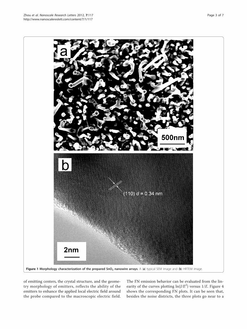
Results and discussionFigure 1a shows a top view SEM image of the in situ-grown SnO2 nanowire arrays. It can be seen that thenanowire was vertically aligned on the silicon substratewith diameters between 40 to 60 nm. Noticeably, on thetop of each nanowire, there was a globule, whichstrongly indicates that the nanowire grew via a vapor-liquid-solid mechanism [19]. The density of the SnO2
nanowire arrays, determined by counting nanowires in arepresentative area of a SEM image, was estimated to be3 × 107/mm2. Figure 1b presents a high-resolution TEMimage of a single SnO2 nanowire. It shows that theSnO2 nanowire is a single crystalline nanowire with aninterplanar spacing of 0.34 nm corresponding to the(110) plane of a rutile crystalline SnO2.XRD characterization was employed to investigate the
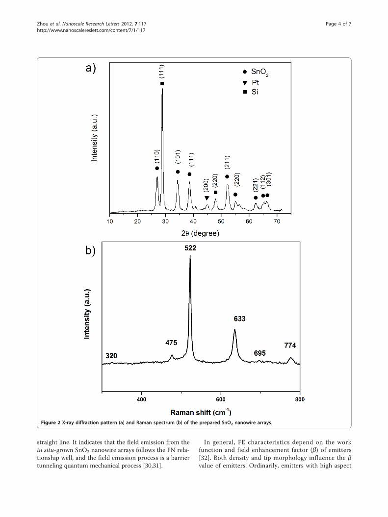
crystal structure of the in situ-grown SnO2 nanowirearrays. Figure 2a shows a typical XRD pattern. The dif-fraction peaks can be well indexed to the standardvalues of bulk SnO2 (JCPDS card: 41-1445), Si (JCPDScard: 27-1402), and Pt (JCPDS card: 88-2343). Thepeaks attributed to SnO2 demonstrate that the in situ-grown sample crystallized with the tetragonal rutilestructure with lattice constants of a = 4.738 Å and c =3.187 Å.A typical room temperature Raman spectrum of the in
situ-grown SnO2 nanowire arrays is shown in Figure 2b.It can be seen that there were three fundamental Ramanpeaks located at 475, 633, and 774 cm-1, which corre-spond to Eg, A1g, and B2g vibration modes, respectively.The results are in good agreement with those of therutile single crystal SnO2 nanowire reported previously[20]. Besides the fundamental Raman peaks, the othertwo Raman peaks located at about 320 and 695 cm-1
were also observed, which correspond to IR-activeEu3TO and A2uLO (TO is the mode of transverse opticalphonons; LO is the mode of longitudinal optical
phonons) modes, respectively [21]. The strong andsharp peak located at about 522 cm-1 corresponds tothe characteristic peak of the silicon substrate [22,23]. Itis believed that the broadening of the peaks in theRaman scattering results is attributed to the quantumconfinement effect of the sample [24].To investigate FE properties of the in situ-grown SnO2
nanowire arrays, FE measurements were performed atvarious anode-cathode separations. Figure 3 presents theFE current density (J) of the in situ-grown SnO2 nano-wire arrays as a function of the applied electric field (E)measured at anode-cathode separations of 100, 150, and200 μm. The turn-on field is defined as the applied elec-tric field which produces a current density distinguishedfrom the background noise (here, defined as 0.01 mAcm-2) [25]. It can be seen from the figure that the turn-on fields were dependent on the anode-cathode distance:their value decreased as the anode-cathode distanceincreased, and the turn-on fields were measured to be2.8, 2.0, and 1.6 V μm-1, respectively. These values arelower than those reported by He et al. [26] (5.8 V μm-1)and Wang et al. [27] (3.77 V μm-1) for the SnO2 nano-wire. The lower turn-on fields may be attributed to thegood alignment of the SnO2 nanowire. Additionally, webelieve that the in situ fabrication method, which madegood electrical contacts between the SnO2 nanowire andthe silicon substrate, contributed greatly to the lowerturn-on fields. Moreover, the emitter radius of the SnO2
nanowire among the arrays was approximately 50 nm,which is small enough to make the FE performanceexcellent [28].In order to understand the emission characteristics, FE
properties were also analyzed by applying the classicFowler-Nordheim [FN] law using the following equation[29]:
J =aE2locϕ
exp(−bϕ3/2
Eloc), (1)
where J is the FE current density, F is the barrierheight of the emission tip surface, and Eloc is the localmicroscopic electric field at the emission sites. The aand b in the equation are constants with value of 1.54 ×10⁻¹⁰ (A V-2 eV) and 6.83 × 10⁹ (V eV-3/2 μm-1), respec-tively. Eloc, which could be up to a hundred or thousandtimes of the macroscopic electric field between the cath-ode and anode, can be calculated using the followingequation:
Eloc = βV
d, (2)
where b is the field enhancement factor, V is theapplied voltage, and d is the anode-cathode separation.The value of b, which is related to the spatial distribution
Zhou et al. Nanoscale Research Letters 2012, 7:117http://www.nanoscalereslett.com/content/7/1/117
Page 2 of 7
of emitting centers, the crystal structure, and the geome-try morphology of emitters, reflects the ability of theemitters to enhance the applied local electric field aroundthe probe compared to the macroscopic electric field.
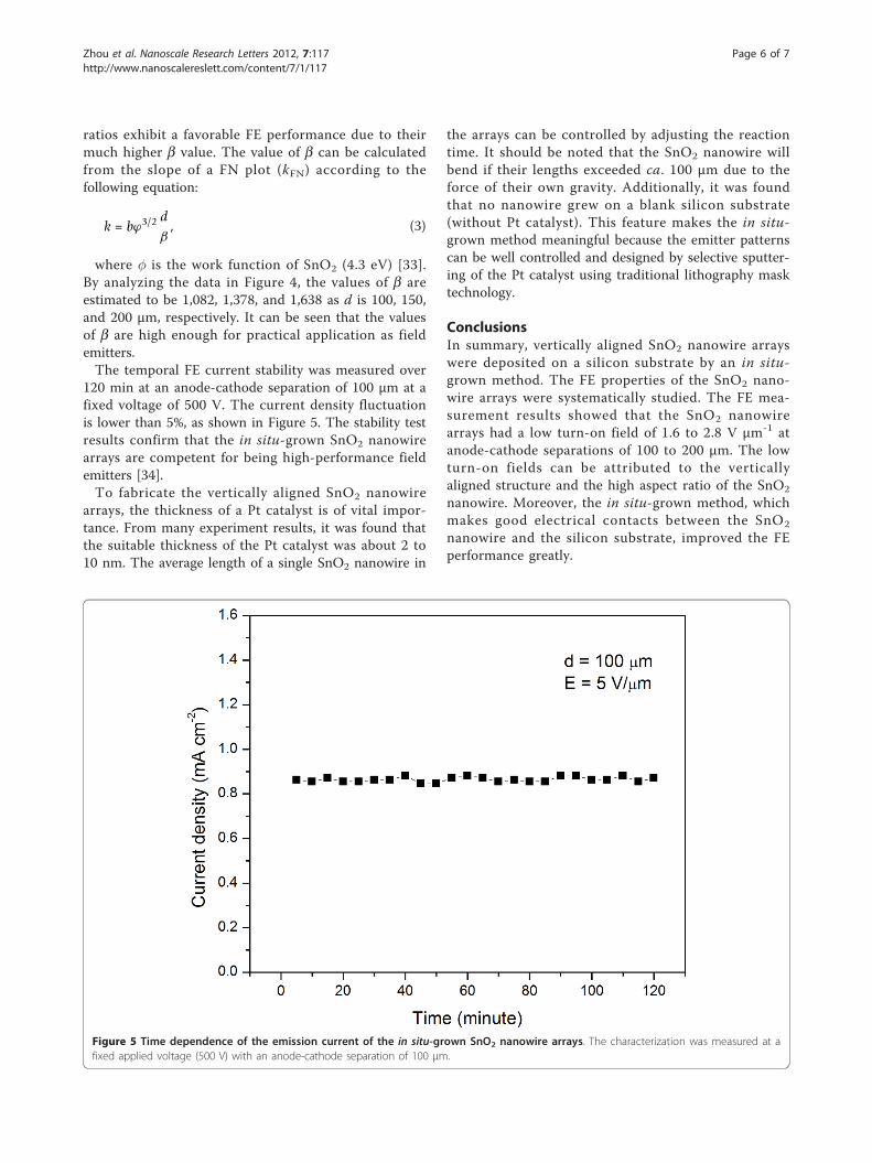
The FN emission behavior can be evaluated from the lin-earity of the curves plotting ln(J/E2) versus 1/E. Figure 4shows the corresponding FN plots. It can be seen that,besides the noise districts, the three plots go near to a
Figure 1 Morphology characterization of the prepared SnO2 nanowire arrays. A (a) typical SEM image and (b) HRTEM image.
Zhou et al. Nanoscale Research Letters 2012, 7:117http://www.nanoscalereslett.com/content/7/1/117
Page 3 of 7
straight line. It indicates that the field emission from thein situ-grown SnO2 nanowire arrays follows the FN rela-tionship well, and the field emission process is a barriertunneling quantum mechanical process [30,31].
In general, FE characteristics depend on the workfunction and field enhancement factor (b) of emitters[32]. Both density and tip morphology influence the bvalue of emitters. Ordinarily, emitters with high aspect
Figure 2 X-ray diffraction pattern (a) and Raman spectrum (b) of the prepared SnO2 nanowire arrays.
Zhou et al. Nanoscale Research Letters 2012, 7:117http://www.nanoscalereslett.com/content/7/1/117
Page 4 of 7
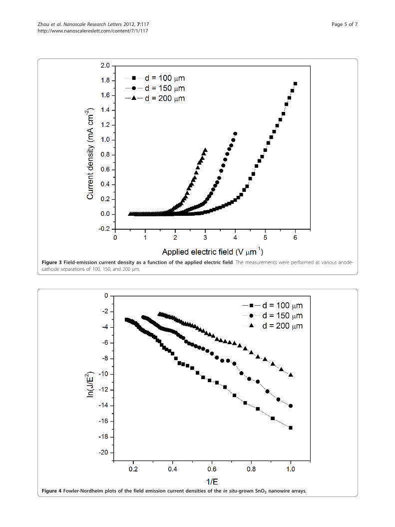
Figure 3 Field-emission current density as a function of the applied electric field. The measurements were performed at various anode-cathode separations of 100, 150, and 200 μm.
Figure 4 Fowler-Nordheim plots of the field emission current densities of the in situ-grown SnO2 nanowire arrays.
Zhou et al. Nanoscale Research Letters 2012, 7:117http://www.nanoscalereslett.com/content/7/1/117
Page 5 of 7
ratios exhibit a favorable FE performance due to theirmuch higher b value. The value of b can be calculatedfrom the slope of a FN plot (kFN) according to thefollowing equation:
k = bϕ3/2 dβ, (3)
where � is the work function of SnO2 (4.3 eV) [33].By analyzing the data in Figure 4, the values of b areestimated to be 1,082, 1,378, and 1,638 as d is 100, 150,and 200 μm, respectively. It can be seen that the valuesof b are high enough for practical application as fieldemitters.The temporal FE current stability was measured over
120 min at an anode-cathode separation of 100 μm at afixed voltage of 500 V. The current density fluctuationis lower than 5%, as shown in Figure 5. The stability testresults confirm that the in situ-grown SnO2 nanowirearrays are competent for being high-performance fieldemitters [34].To fabricate the vertically aligned SnO2 nanowire
arrays, the thickness of a Pt catalyst is of vital impor-tance. From many experiment results, it was found thatthe suitable thickness of the Pt catalyst was about 2 to10 nm. The average length of a single SnO2 nanowire in
the arrays can be controlled by adjusting the reactiontime. It should be noted that the SnO2 nanowire willbend if their lengths exceeded ca. 100 μm due to theforce of their own gravity. Additionally, it was foundthat no nanowire grew on a blank silicon substrate(without Pt catalyst). This feature makes the in situ-grown method meaningful because the emitter patternscan be well controlled and designed by selective sputter-ing of the Pt catalyst using traditional lithography masktechnology.
ConclusionsIn summary, vertically aligned SnO2 nanowire arrayswere deposited on a silicon substrate by an in situ-grown method. The FE properties of the SnO2 nano-wire arrays were systematically studied. The FE mea-surement results showed that the SnO2 nanowirearrays had a low turn-on field of 1.6 to 2.8 V μm-1 atanode-cathode separations of 100 to 200 μm. The lowturn-on fields can be attributed to the verticallyaligned structure and the high aspect ratio of the SnO2
nanowire. Moreover, the in situ-grown method, whichmakes good electrical contacts between the SnO2
nanowire and the silicon substrate, improved the FEperformance greatly.
Figure 5 Time dependence of the emission current of the in situ-grown SnO2 nanowire arrays. The characterization was measured at afixed applied voltage (500 V) with an anode-cathode separation of 100 μm.
Zhou et al. Nanoscale Research Letters 2012, 7:117http://www.nanoscalereslett.com/content/7/1/117
Page 6 of 7
AcknowledgementsThis work was primarily supported by the Scientific Research StartingFoundation for Outstanding talent, University of Electronic Science andTechnology of China.
Authors’ contributionsZHZ conducted all the experiments and drafted the manuscript. JWprovided helpful guidance and suggestions. HDL helped in drafting themanuscript. ZMW supervised all of the study. All authors read and approvedthe final manuscript.
Competing interestsThe authors declare that they have no competing interests.
Received: 11 December 2011 Accepted: 13 February 2012Published: 13 February 2012
References1. Gubbala S, Chakrapani V, Kumar V, Sunkara MK: Band-edge engineered
hybrid structures for dye-sensitized solar cells based on SnO2 nanowires.Adv Funct Mater 2008, 18:2411-2418.
2. Wan Q, Huang J, Xie Z, Wang TH, Dattoli EN, Lu W: Branched SnO2
nanowires on metallic nanowire backbones for ethanol sensorsapplication. Appl Phys Lett 2008, 92:102101.
3. Sysoev VV, Goschnick J, Schneider T, Strelcov E, Kolmakov A: A gradientmicroarray electronic nose based on percolating SnO2 nanowire sensingelements. Nano Lett 2007, 7:3182-3188.
4. Kim H, Cho J: Hard templating synthesis of mesoporous and nanowireSnO2 lithium battery anode materials. J Mater Chem 2008, 18:771-775.
5. Wang S, Cheng G, Cheng K, Jiang X, Du Z: The current image of singleSnO2 nanobelt nanodevice studied by conductive atomic forcemicroscopy. Nanoscale Res Lett 2011, 6:541.
6. Ying Z, Wan Q, Song ZT, Feng SL: SnO2 nanowhiskers and their ethanolsensing characteristics. Nanotechnology 2004, 15:1682-1684.
7. Zhu SM, Zhang D, Gu JJ, Xu JQ, Dong JP, Li JL: Biotemplate fabrication ofSnO2 nanotubular materials by a sonochemical method for gas sensors.J Nanopart Res 2010, 12:1389-1400.
8. Wang GX, Park JS, Park MS: Growth, characterization and technologicalapplications of semiconductor SnO2 nanotubes and In2O3 nanowires. JNanosci Nanotechnol 2009, 9:1144-1147.
9. Wang YL, Guo M, Zhang M, Wang XD: Hydrothermal synthesis of SnO2
nanoflower arrays and their optical properties. Scripta Mater 2009,61:234-236.
10. El-Etre AY, Reda SM: Characterization of nanocrystalline SnO2 thin filmfabricated by electrodeposition method for dye-sensitized solar cellapplication. Appl Surf Sci 2010, 256:6601-6606.
11. Zhang YS, Yu K, Li GD, Peng DY, Zhang QX, Xu F, Bai W, Ouyang SX,Zhu ZQ: Synthesis and field emission of patterned SnO2 nanoflowers.Mater Lett 2006, 60:3109-3112.
12. Li LJ, Zong FJ, Cui XD, Ma HL, Wu XH, Zhang QD, Wang YL, Yang F,Zhao JZ: Structure and field emission properties of SnO2 nanowires.Mater Lett 2007, 61:4152-4155.
13. Jang HS, Kang SO, Kim YI: Enhancement of field emission of SnO2
nanowires film by exposure of hydrogen gas. Solid State Commun 2006,140:495-499.
14. Wu J, Yu K, Li LJ, Xu JW, Shang DJ, Xu YE, Zhu ZQ: Controllable synthesisand field emission properties of SnO2 zigzag nanobelts. J Phys D ApplPhys 2008, 41:185302.
15. Bhise AB, Late DJ, Ramgir NS, More MA, Mulla IS, Pillai VK, Joag DS: Fieldemission investigations of RuO2-doped SnO2 wires. Appl Surf Sci 2007,253:9159-9163.
16. Fang XS, Bando Y, Gautam UK, Ye C, Golberg D: Inorganic semiconductornanostructures and their field-emission applications. J Mater Chem 2008,18:509-522.
17. Pan W, He XW, Chen Y: Preparation and characterization ofpolyacrylonitrile/antimony doped tin oxide composite nanofibers byelectrospinning method. Optoelectron Adv Mat 2010, 4:390-394.
18. Liu J, Li Y, Huang X, Zhu Z: Tin oxide nanorod array-basedelectrochemical hydrogen peroxide biosensor. Nanoscale Res Lett 2010,5:1177-1181.
19. Barth S, Hernandez-Ramirez F, Holmes JD, Romano-Rodriguez A: Synthesisand applications of one-dimensional semiconductors. Prog Mater Sci2010, 55:563-627.
20. Gu F, Wang SF, Cao HM, Li CZ: Synthesis and optical properties of SnO2
nanorods. Nanotechnology 2008, 19:095708.21. Zheng MJ, Ma L, Xu WL, Ding GQ, Shen WZ: Preparation and structural
characterization of nanocrystalline SnO2 powders. Appl Phys A-mater2005, 81:721-723.
22. Nakashima S, Oima S, Mitsuishi A, Nishimura T, Fukumoto T, Akasaka Y:Raman scattering study of ion implanted and C.W.-Laser annealedpolycrystalline silicon. Solid State Commun 1981, 40:765-768.
23. Li LJ, Yu K, Mao HB, Zhu ZQ: Photoluminescence and field-emissionproperties of Cu-doped SnO2 nanobelts. Appl Phys A-mater 2010,99:865-869.
24. Sun S: Raman scattering study of rutile SnO2 nanobelts synthesized bythermal evaporation of Sn powders. Chem Phys Lett 2003, 376:103-107.
25. Li M-K, Wang D-Z, Ding Y-W, Guo X-Y, Ding S, Jin H: Morphology and fieldemission from ZnO nanowire arrays synthesized at differenttemperature. Mat Sci Eng A-struct 2007, 452-453:417-421.
26. He JH, Wu TH, Hsin CL, Li KM, Chen LJ, Chueh YL, Chou LJ, Wang ZL:Beaklike SnO2 nanorods with strong photoluminescent and field-emission properties. Small 2006, 2:116-120.
27. Wang JB, Li K, Zhong XL, Zhou YC, Fang XS, Tang CC, Bando Y:Considerable enhancement of field emission of SnO2 nanowires bypost-annealing process in oxygen at high temperature. Nanoscale ResLett 2009, 4:1135-1140.
28. Zheng X, Chen G, Li Z, Deng S, Xu N: Quantum-mechanical investigationof field-emission mechanism of a micrometer-long single-walled carbonnanotube. Phys Rev Lett 2004, 92:106803.
29. Zhang YA, Lin JY, Guo TL: Fabrication and properties of film-under-gatefield emission arrays with SnO2 emitters for flat lamp. Appl Surf Sci 2010,257:306-311.
30. de Heer WA, Châtelain A, Ugarte D: A carbon nanotube field-emissionelectron source. Science 1995, 270:1179-1180.
31. Li LA, Cheng SH, Li HD, Yu Q, Liu JW, Lv XY: Effect of nitrogen ondeposition and field emission properties of boron-doped micro- andnano-crystalline diamond films. Nano-Micro Lett 2010, 2:154-159.
32. Sheini FJ, Singh J, Srivasatva ON, Joag DS, More MA: Electrochemicalsynthesis of Cu/ZnO nanocomposite films and their efficient fieldemission behaviour. Appl Surf Sci 2010, 256:2110-2114.
33. Luo S, Chu PK, Di Z, Zhang M, Liu W, Lin C, Fan J, Wu X: Vacuum electronfield emission from SnO2 nanowhiskers annealed in N2 and O2
atmospheres. Appl Phys Lett 2006, 88:013109.34. Xue XY, Li LM, Yu HC, Chen YJ, Wang YG, Wang TH: Extremely stable field
emission from AlZnO nanowire arrays. Appl Phys Lett 2006, 89:043118.
doi:10.1186/1556-276X-7-117Cite this article as: Zhou et al.: Field emission from in situ-grownvertically aligned SnO2 nanowire arrays. Nanoscale Research Letters 20127:117.
Submit your manuscript to a journal and benefi t from:
7 Convenient online submission
7 Rigorous peer review
7 Immediate publication on acceptance
7 Open access: articles freely available online
7 High visibility within the fi eld
7 Retaining the copyright to your article
Submit your next manuscript at 7 springeropen.com
Zhou et al. Nanoscale Research Letters 2012, 7:117http://www.nanoscalereslett.com/content/7/1/117
Page 7 of 7