Embed Size (px)
Citation preview

Journal of Ceramic Processing Research. Vol. 9, No. 3, pp. 282~285 (2008)
282
J O U R N A L O F
CeramicProcessing Research
Field effect transistor properties of ZnO nanowires
Kyoung-Won Kima, Won-Seok Oha, Gun-Eik Janga,*, Dong-Won Parkb,c, Jeong-O Leeb and Beom-Soo Kimc
aDepartment of Advanced Materials Engineering, CBITRC, Chungbuk National University, Cheongju 361-763, KoreabFusion Biotechnology Research Center, Korea Research Institute of Chemical Technology, Daejeon 305-343, KoreacDepartment of Chemical Engineering, Chungbuk National University, Cheongju 500-712, Korea
Zinc oxide (ZnO) nanostructures were grown on Si (001) substrates by thermal chemical vapor deposition without anycatalysts. The deposition temperatures varied from 800 oC to 1100 oC. SEM and XRD data suggest the nanostructures are well-aligned, single ZnO crystals with a (0002) preferential orientation. Back-gate ZnO nanowire field effect transistors (FET) werealso successfully fabricated using a photolithography process. The fabricated nanowire FET exhibited Ohmic contact betweenthe ZnO nanowire channels and Au metal electrodes. The ZnO nanowire exhibited n-type field effect transistor behaviordenoted by an increase in current with increasing gate voltage.
Key words: Thermal CVD, Zinc Oxide, Nanostructures, and FET.
Introduction
Zinc oxide (ZnO) has: a hexagonal structure, latticeconstants of a = 0.324-0.326 nm and c = 0.513-0.543 nm,a wide band-gap of 3.37 eV, and a large exciton bindingenergy of 60 MeV at room temperature [1-3]. The synthesisof semiconducting, nanostructure materials has been carriedout in graphitic nanotubes [4]. Compound semiconductingnanomaterials including GaN [5], GaP [6], InP [7], ZnO[8, 9], and Ga2O3 [10] have also been developed for thefabrication of nano-optoelectronic devices. ZnO has beenattracting considerable attention for such optoelectronicsapplications as transparent thin film transistors (TFT),field effect transistors (FET), and ultraviolet light emittingdevices (LED). A light emitting diode of a single ZnOcrystal is expected to have high energy efficiency due inpart to its intense band edge luminescence upon laserexcitation [11] and its photoluminescence (PL) spectrumshowing blue emission at 380 nm. In particular, theelectronic properties of semiconductor surfaces are stronglyaffected by the chemical adsorption of ambient gases[12-15]. Wide band-gap nanowires have attracted muchinterest owing to their remarkable chemical and physicalproperties [16]. High quality polycrystalline ZnO nanowiresprepared by thermal CVD on silicon substrate have beenreported [1-3, 8, 9].
The interest in field effect transistors (FET) has drasticallyincreased over the past few years and extensively studiedfor many potential applications ranging from displays andidentification tags to sensors [17]. In particular, theapplication of nanowires to FET has been intensely
researched due to the various advantages nanowires have,including good transportation of charge and high crystallinequality [18]. Currently, photolithography employing ZnOnanowire FETs based on back-gate structures is used tofabricate many nanowire FETs. In integrated devices, itis impossible to individually control each back-gate FET[19]. In this study, a fabrication technique is developedfor back-gate nanowires FETs using photolithography.The electrical properties of the top- and back-gate ZnOnanowire FETs are characterized by conventional I-Vmeasurements.
Experimental
ZnO nanowires were grown on silicon substratesusing thermal chemical vapour deposition (CVD). ZnOnanowires were synthesized by thermally vaporizing amixture of commercial ZnO powder (99.999%) and graphitepowder (99%) in a 1:1 ratio in a quartz tube furnacewith silicon (100) as the substrate for nanowire growth.The Si substrate (10 mm × 10 mm) was placed facedownon an aluminum, ceramic boat loaded with a mixture ofthe powders at a thickness of approximately 2 mm. Theboat [15 mm × 15 mm × 400 mm] was inserted into thetube of the quartz furnace under a constant flow ofargon (40 sccm) and oxygen (20 sccm) and heated upto 800-1100 oC for 30 minutes. Figure 1 shows a schematicof the Thermal CVD system used for the deposition ofthe ZnO nanowires. No catalyst was utilized in any ofthe deposition processes.
To fabricate the ZnO nanowire FET device, ZnOnanowires grown on the Si substrate were transferredfrom the substrate to a silicon wafer using a 500 nm thick,thermally grown oxide, made by dropping a nanowiresuspension in water. The nanowire suspension was made
*Corresponding author: Tel : +82-43-261-2412Fax: +82-43-271-3222E-mail: [email protected]
Field effect transistor properties of ZnO nanowires 283
by brief sonication of the substrate with ZnO nanowireson its surface in water for 10-20 s. Maker patterns werefabricated in order to indicate the position of the nanowiresand to serve as alignment makers. First, a photoresist layerwas spin-coated on a maker Si (100) substrate. Second,the photoresist layer was fabricated using a photolithographyprocess employing a lift-off process using a PR removersolution [20, 21]. Finally, metal electrodes consisting ofTi (4 nm)/Au (12 nm) were deposited by an evaporator,giving a final distance of 1-2 μm between the source anddrain electrode.
The crystalline phases of the thin films were identifiedby an X-ray diffractometer (Scintag SDS 2000) whilemicrostructure and surface roughness were observed bya field emission scanning electron microscope (HitachiS 2500C). The electrical properties of the FET were studiedat room temperature by a prove station (national instrument).
Results and Discussion
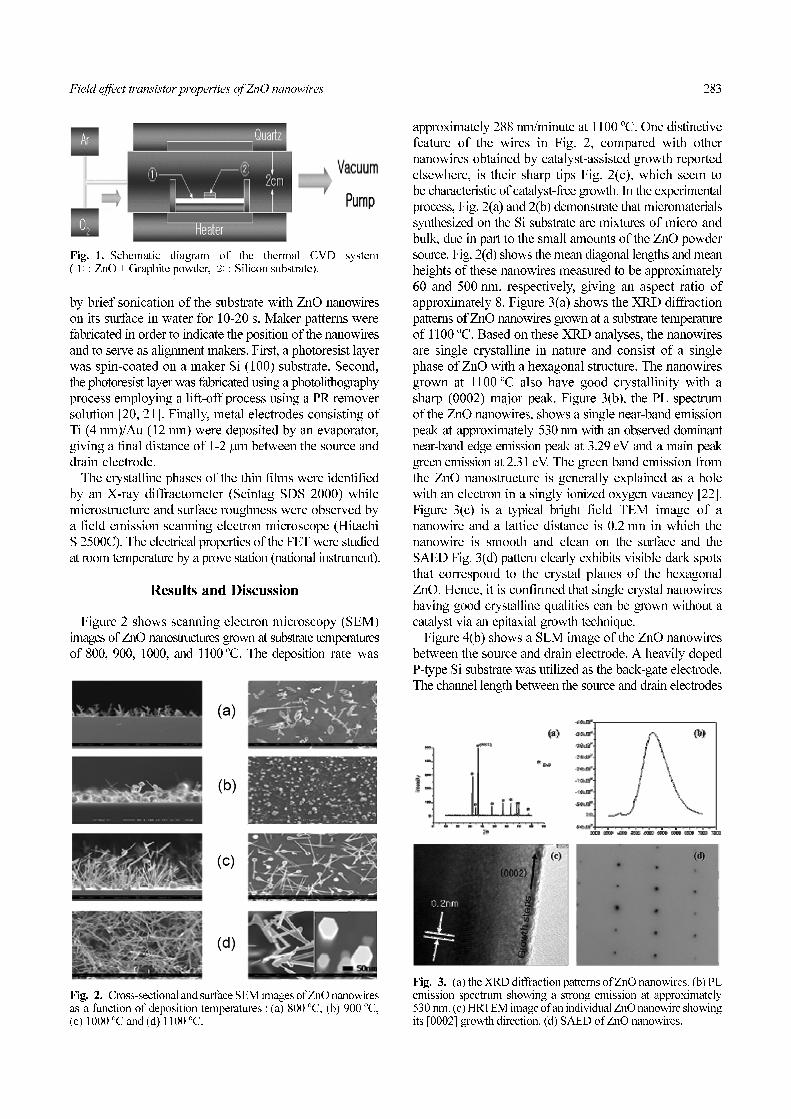
Figure 2 shows scanning electron microscopy (SEM)images of ZnO nanostructures grown at substrate temperaturesof 800, 900, 1000, and 1100 oC. The deposition rate was
approximately 288 nm/minute at 1100 oC. One distinctivefeature of the wires in Fig. 2, compared with othernanowires obtained by catalyst-assisted growth reportedelsewhere, is their sharp tips Fig. 2(c), which seem tobe characteristic of catalyst-free growth. In the experimentalprocess, Fig. 2(a) and 2(b) demonstrate that micromaterialssynthesized on the Si substrate are mixtures of micro andbulk, due in part to the small amounts of the ZnO powdersource. Fig. 2(d) shows the mean diagonal lengths and meanheights of these nanowires measured to be approximately60 and 500 nm, respectively, giving an aspect ratio ofapproximately 8. Figure 3(a) shows the XRD diffractionpatterns of ZnO nanowires grown at a substrate temperatureof 1100 oC. Based on these XRD analyses, the nanowiresare single crystalline in nature and consist of a singlephase of ZnO with a hexagonal structure. The nanowiresgrown at 1100 oC also have good crystallinity with asharp (0002) major peak. Figure 3(b), the PL spectrumof the ZnO nanowires, shows a single near-band emissionpeak at approximately 530 nm with an observed dominantnear-band edge emission peak at 3.29 eV and a main peakgreen emission at 2.31 eV. The green band emission fromthe ZnO nanostructure is generally explained as a holewith an electron in a singly ionized oxygen vacancy [22].Figure 3(c) is a typical bright field TEM image of ananowire and a lattice distance is 0.2 nm in which thenanowire is smooth and clean on the surface and theSAED Fig. 3(d) pattern clearly exhibits visible dark spotsthat correspond to the crystal planes of the hexagonalZnO. Hence, it is confirmed that single crystal nanowireshaving good crystalline qualities can be grown without acatalyst via an epitaxial growth technique.
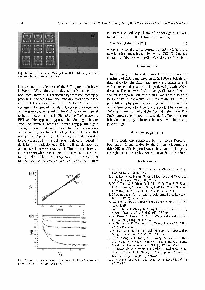
Figure 4(b) shows a SEM image of the ZnO nanowiresbetween the source and drain electrode. A heavily dopedP-type Si substrate was utilized as the back-gate electrode.The channel length between the source and drain electrodes
Fig. 1. Schematic diagram of the thermal CVD system(① : ZnO + Graphite powder, ② : Silicon substrate).
Fig. 2. Cross-sectional and surface SEM images of ZnO nanowiresas a function of deposition temperatures : (a) 800 oC, (b) 900 oC,(c) 1000 oC and (d) 1100 oC.
Fig. 3. (a) the XRD diffraction patterns of ZnO nanowires. (b) PLemission spectrum showing a strong emission at approximately530 nm. (c) HRTEM image of an individual ZnO nanowire showingits [0002] growth direction. (d) SAED of ZnO nanowires.
284 Kyoung-Won Kim, Won-Seok Oh, Gun-Eik Jang, Dong-Won Park, Jeong-O Lee and Beom-Soo Kim
is 1 μm and the thickness of the SiO2 gate oxide layeris 500 nm. We evaluated the device performance of theback-gate nanowire FET fabricated by the photolithographyprocess. Figure 5(a) shows the Ids-Vds curves of the back-gate FET for Vg ranging from −1 V to 1 V. The drainvoltage and slopes of the Ids-Vds curves are dependenton the gate voltage, revealing the ZnO nanowire channelto be n-type. As shown in Fig. (5), the ZnO nanowireFET exhibits typical n-type semiconducting behaviorsince the current increases with increasing positive gatevoltage, whereas it decreases down to a few picoampereswith increasing negative gate voltage. It is well known thatundoped ZnO generally exhibits n-type conduction dueto the presence of intrinsic donor-type defects induced bydeviation from stoichiometry [23]. The linear characteristicof the Ids-Vds curves shows there is Ohmic contact betweenthe ZnO nanowire channel and the Au metal electrodes.In Fig. 5(b), within the Ids-Vg curve, the drain currentIds increases as the gate voltage, Vg, varies from −10 V
to +10 V. The oxide capacitance of the back-gate FET wasfound to be 3.71 × 10⁻¹¹ F from the equation,
C = 2πεrε0L/ln(2h/r) [24] (1)
where εr is the dielectric constant of SiO2 (3.9), L thegate length (1 μm), h the thickness of SiO2 (500 nm), rthe radius of the nanowire (60 nm), and ε0 is 8.85 × 10⁻¹².
Conclusions
In summary, we have demonstrated the catalyst-freesynthesis of ZnO nanowires on an Si (100) substrate bythermal CVD. The ZnO nanowire was a single crystalwith a hexagonal structure and a preferred growth (0002)direction. The nanowires had an average diameter of 60 nmand an average length of 500 nm. We were also ableto fabricate a back-gate ZnO nanowire FET by aphotolithography process, yielding an FET exhibitingohmic (semiconductor + conductor) contact between theZnO nanowire channel and the Au metal electrode. TheZnO nanowire exhibited a n-type field effect transistorbehavior denoted by an increase in current with increasinggate voltage.
Acknowledgements
“This work was supported by the Korea ResearchFoundation Grant funded by the Korean Government(MOEHRD)” (The Regional Research Universities Program/Chungbuk BIT Research-Oriented University Consortium).
References
1. C.-J. Lee, T.-J. Lee, S.-C. Lyu and Y. Zhang, Appl. Phys.Lett. 81 (2002) 3648-3650.
2. J.-S. Lee, M.-I. Kanga, S. Kim, M.-S. Lee and Y.-K. Lee,J. Cryst. Growth 249 (2003) 201-207.
3. H.-J. Yuan, S.-S. Yuan, D.-F. Liu, X.-Q. Yan, Z.-P. Zhou,L. Ci, J. Wang, Y. Gao, L. Song, L.-F. Liu, W.-Y. Zhou andG. Wang, Chem. Phys. Lett. 371 (2003) 337-341.
4. N. Hamada, S. Sawada and A. Oshiyama, Phys. Rev. Lett.68[10] (1992) 1579-1581.
5. W. Han, S. Fan, Q. Li and Y. Hu, Science. 277[5330] (1997)1287-1289.
6. W.-S. Shi, Y.-F. Zheng, N. Wang, C.-S. Lee and S.-T. Lee,Chem. Phys. Lett. 345[5-6] (2001) 377-380.
7. X. Duan, Y. Huang, Y. Cui, J. Wang and C.-M. Lieber,Nature 409[6816] (2001) 66-69.
8. Z.-W. Pan, Z.-R. Dai and Z.-L. Wang, Science 291[5510](2001) 1947-1949.
9. M.-H. Huang, Y. Wu, H. Feick, N. Tran, E. Weber and P.Yang, Adv. Mater. 13[2] (2001) 113-116.
10. H.-Z. Zhang, Y.-C. Kong, Y.-Z. Wang, X. Du, Z.-G., Bai,J.-J. Wang, P.-D. Yu, Y. Ding, Q.-L. Hang and S.-Q. Feng,Solid State Communication 109[11] (1999) 677-682.
11. M. Kawasaki, A. Ohtomo, I. Ohkubo, H. Koinumal, Z.-K.Tang, P. Yu, G.-K.-L. Wong, B.-P. Zhang and Y. Segawa,Mat. Sci. Eng. B56 (1998) 239-245.
12. J.-B. Baxter and E.-S. Aydil, Appl. Phys. Lett. 86, 053114(2005) 1-3.
Fig. 4. (a) Real picture of Mask pattern, (b) SEM image of ZnOnanowire between source and drain.
Fig. 5. (a) Ids-Vds curves of the back-gate FET for Vg rangingfrom −1 V to 1 V (b) Ids-Vg curves.

Field effect transistor properties of ZnO nanowires 285
13. W. Monch, J. Vac Sic. Technol. 7 (1989) 1216-1219.14. A. Many, Y. Goldstein and N.-B. Grover, Semiconductor
Surfaces, North-Holland, Amsterdam, 1965.15. W. Monch, Semiconductor Surface and Interfaces, 3rd ed.,
Springer, Berlin (2001).16. Y. Cui, Q. Wei, H.-K. Park, and C.-M. Lieber, Science 293
(2001) 1289-1292.17. C. Dimitrakopoulos and P.-R.-L.-M. Malenfant, Adv.
Mater. 14 (2002) 99-99.18. J. Hu, T.-W. Odom and C.-M. Lieber, Acc. Chem. Res. 32
(1999) 435-445.19. S. Ju, K. Lee, D.-B. Janes, M. Yoon, A. Facchetti and T.-J.
Marks, Nano Lett. 5 (2005) 2281-2286.
20. K. Keem, J.-M. Kang, C.-J. Yoon, D.-H. Yeom, D.-Y. Jeongand B.-M. Moon, Micro. Eng. 84 (2007) 1622-1626.
21. W.-K. Hong, B.-J. Kim, T.-W. Kim, G.-H. Jo, S.-H. Songand S.-S. Kwon, Colloids and Surfaces A 313-314 (2007)378-382.
22. K. Vanhausden, W.-L. Warren, C.-H. Seager, D.-R. Tallant,J.-A. Voigt and B.-E. Gande, J. Appl. Phys. 79 (1996)7983-7990.
23. D.-C. Look, J.-W. Hemsky and J.-R Sizelove, Phys. Rev.Lett. 82 (1999) 2552-2555.
24. Y. Huang, X. Duan, Y. Cui and C.-M. Lieber, Nano Lett. 2(2002) 101-104.