Embed Size (px)
Citation preview

AD-A242 977 rff11 l l!!111 Im ll! illillll!l
Technical Report 1439July 1991
ATV Encoder andDecoder MonitorCircuits
C. A. KunitakeW. S. MorinagaK. Perreira
91-17095II filt E v l! Approved for public release: distribution is unlimited.
in i | O i |i • ||

NAVAL OCEAN SYSTEMS CENTERSan Diego, California 92152-5000
J. D. FONTANA, CAPT, USN R. T. SHEARER, ActingCommander Technical Director
ADMINISTRATIVE INFORMATION
This report was prepared during the period of January 1991 to May 1991. The workwas conducted under project MS09, program element 603713N, and work unitDN188508. The responsible organization was the Naval Sea Systems Command,Washington, DC 20362; and the work was performed by Code 534 (Hawaii) of theNaval Ocean Systems Center, San Diego, CA 92152-5000.
Released by Under authority ofA. T. Nakagawa, Head D. W Murphy, HeadFiber-Optic and Electronic Advanced SystemsSystems Branch Division
RBT

SUMMARY
OBJECTIVES
This report was produced to describe the circuits the Advanced Tethered Vehicle(ATV) system employs to monitor the telemetered signals between the surface of theocean and the submersible vehicle. An additional objective of the report was to explainhow these ATV system circuits facilitate in troubleshooting the system.
RESULTS
During initial checkout of the ATV system and throughout the systems tests, theencoder monitor and decoder monitor circuits clearly demonstrated their worth indetecting and troubleshooting problems. In many cases, by using these circuits, malfunc-tions were rapidly isolated to the surface equipment or to the vehicle equipment. Thus,these monitoring circuits have proven effective in decreasing the ATV system's mean timeto repair (MTTR).
RECOMMENDATIONS
In addition to using these monitoring circuits with the Loral encoder and decoderunits, with some modification, these circuits can also be used to monitor other similartelemetry systems employing digitally multiplexed data.
* <' Is , .-
<, 4,

CONTENTS
INTRODUCTION AND GENERAL DESCRIPTION .......................... 1
ATV DESCRIPTION ................................................. 1
SC O PE ............................................................ 1
ATV FIBER-OPTIC TELEMETRY DESCRIPTION ........................... 3
DOWNLINK TELEMETRY CHANNEL .................................. 4
UPLINK TELEMETRY CHANNEL ..................................... 4
LORAL ENCODER AND DECODER ................................... 5
FUNCTION OF THE MONITOR CIRCUITS ................................ 7
ENCODER MONITOR CIRCUIT ....................................... 8
CIRCUIT DESCRIPTION ............................................. 9
TIMING CIRCUIT ........................................... 13
DECODER MONITOR CIRCUIT ...................................... 13
CIRCUIT DESCRIPTION ............................................ 15
TIM ING CIRCUIT .................................................. 17
EFFECTIVENESS OF CIRCUITS ........................................ 19
ATV SYSTEM APPLICATION ........................................ 19
OTHER APPLICATIONS ............................................ 19
FIGURES
1. ATV system concept . ................................................ 2
2. ATV telemetry system, block diagram . ................................. 3
3. Downlink telemetry channel, block diagram .............................. 4
4. Uplink telemetry channel, block diagram ................................ 5
5. Telemetry status check scheme . ....................................... 8
6. M onitor circuit, block diagram ......................................... 9
7. Command monitor, schematic diagram ................................. 11
8. Encoder monitor circuit, timing diagram . .............................. 14
9. Instrumentation monitor, schematic diagram ............................ 16
10. Decoder monitor circuit, timing diagram ............................... 18
iii

INTRODUCTION AND GENERAL DESCRIPTION
ATV DESCRIPTION
The Advanced Tethered Vehicle (ATV) system was developed and tested by the NavalOcean Systems Center, Hawaii Laboratory. The ATV is a remotely operated submersiblesystem designed to perform general work missions down to ocean depths of 20,000 feet.Figure 1 shows the overall ATV system concept. It consists of five main components: (1)the submersible vehicle, (2) the tether cable, (3) the handling system, (4) the control van,and (5) the auxiliary equipment.
The submersible vehicle performs work missions such as installation, maintenance,repair, rescue, or recovery. To perform its mission, the vehicle has two state-of-the-art,
position-controlled, force-feedback manipulators, and a variety of tools. Six TV cameras,including a stereo pair, provide visual feedback. To guide the vehicle to the work site, theoperator employs five thrusters and various sensors onboard the vehicle, and a deepocean navigation system.
A tether cable, attached to the vehicle, transmits power to the vehicle and also signalsbetween it and the surface. The tether cable consists of three electrical conductors, threeoptical fibers, and Kevlar strength members. Signals are multiplexed over one of the threeoptical fibers, while power is transmitted over the three electrical conductors.
At the surface, the handling system launches and recovers the vehicle, and managesthe tether cable. The control van houses the operators and the consoles that control thesystem. It also contains the electronics that operate the vehicle and communicate with it.Included in the auxiliary equipment are two electrical generators that supply power to thesystem and also to the maintenance facilities.
SCOPE
This report describes the circuits the ATV system employs to monitor the telemeteredsignals between the surface and the submersible vehicle. These circuits provide on-linechecking of the individual bits in the serial data stream. The ATV telemetry subsystem isalso described to show the correlation and importance of the monitor circuits to the sys-tem. The telemetry subsystem is presented first, followed by a description of the monitorcircuits and their relationships. The report also explains how these circuits facilitatetroubleshooting the system.

SURFACE
LIFT LINE
AUXILIARYEQUIPMENT
TETHERCABLE
~ SUBMERSIBLEa t - VHICLE . ...
Figure 1. ATV system concept.
2

ATV FIBER-OPTIC TELEMETRY DESCRIPTION
This telemetry system (figure 2) utilizes wavelength division multiplexing to provide afull-duplex communications system. The downlink optical wavelength is 1.55 microns,while the uplink optical wavelength is 1.3 microns. Commands are transmitted from thesurface to the vehicle on the downlink telemetry channel, while vehicle instrumentationdata and videos are transmitted from the vehicle to the surface on the uplink channel. Allthe telemetered signals are digitized, serially multiplexed, converted to an optical signal,and transmitted to the receiver. At the receiver, the optical signal is reconverted to anelectrical signal, and the demultiplexer outputs the original input signals.
SURFACEr--- -- --------------
COMMAND _ _W DDOWNLINK DOWNLINK OPTICAL
INPUT MULTIPLEXER TAL"7- DUPLXERSIGNALS
I UPLINK UPLINKOUTPUT DEMULTIPLEXER RECIVERSIGNALS
OPTICAL FIBER
VEHICLE
OPTICAL DOWNLINK DWLN --- DWLNX------- OPTICAL ------- --- OUTP
RECEIVER DEMULTIPLEXERSIGNALS
UPLINKVIE&
OPTICAL UPLINK UPLINKTRANSMITTER MULTIPLEXER INPUTI 1SIGNALS
Figure 2. ATV telemetry system, block diagram.
3

DOWNLINK TELEMETRY CHANNEL
The downlink channel is illustrated in figure 3. Signals transmitted from the surface tothe vehicle are the vehicle commands, sonar commands, manipulator commands, andemergency commands. The vehicle command signals are low frequency signals that in-clude digital control signals for switching lights, motors, or solenoid valves; and analogcontrol signals for proportional control of servo valves. These vehicle commands are digit-ized and multiplexed into a 20-kbps bit stream by the PCM-440A Encoder manufacturedby Loral Data Systems. This 20-kbps bit stream and the other commands are multiplexedby a Universal Asynchronous Receiver/Transmitter (UART). The UART's multiplexedoutput goes to the 1.55-micron optical transmitter.
At the vehicle, the 1.55-micron optical signal is launched into an optical receiver thatconverts this optical signal back to an electrical one. The signal is then routed to a UARTdemultiplexer. The vehicle command signal output from the UART is sent to theAPD-44A Decoder manufactured by Loral Data Systems. This decoder demultiplexes the20-kbps bit stream and outputs the individual analog and digital control signals.
COMMAND- ENCODER1 MULIPEXR TRANSMTR FIBER RECEIVER DMLIEX DECODER COMMANDINPUTOUTPUT
LEFT MANIPULATOR DOWNLINK LEFT MANIPULATOR DOWNLINKRIGHT MANIPULATOR DOWNLINK RIGHT MANIPULATOR DOWNIUNK
SONAR DOWNLINK LI*SONAR DOWNLINKEMERGENCY COMMANDS EMERGENCY COMMANDS
Figure 3. Downlink telemetry channel, block diagram.
UPLINK TELEMETRY CHANNEL
The uplink channel (figure 4) transmits two realtime videos, sonar uplink data, twomanipulator uplink data, and vehicle instrumentation data. Similar to the downlink chan-nel, the uplink telemetry channel serially multiplexes the various signals and converts thisserial digital signal to an optical signal. The difference is that the the uplink optical wave-length is 1.3 micron. At the surface, the optical receiver reconverts the optical signal backto an electrical signal. This serial digital signal is then demultiplexed, and the originalinput signals are reproduced.
4

F I UPLINK
INSTRUMENTATION 1.3ASDATA (ANALOG & EN---E- OTICAIGDGTLIPT) -- ENCODER MULTIPLEXER -= MULTIPLEXER TRASITTERDIGITAL INPUTS) .TRN f/E
RIGHT MANIPULATORI UPLINK DATA VIDEO 2--
SONAR UPUNK DATA
OPTICALFIBER
1.3 ~~UPLINK ----
OI.3 HIGH SPEED DATA DIGITAL LORA 1INSTRUMENTATIONRECEIVER DEMULTIPLEXER DEMULTIPLEXER OR - - DATA (ANALOG &
VIDEO 1 LEFT MANIPULATOR UPLINK DATA
VIDEO 2 RIGHT MANIPULATOR UPLINK DATASONAR UPLINK DATA
Figure 4. Uplink telemetry channel, block diagram.
Like the vehicle command signals in the downlink channel, the vehicle instrumentationsignals are multiplexed by the Loral PCM-440A Encoder, and demultiplexed by the LoralAPD-444A Decoder. The vehicle instrumentation data are the low frequency vehicle statusand sensor signals, such as heading, altitude, pressure, and temperature data. The instru-mentation serial bit stream from the encoder, along with the two manipulator uplink dataand the sonar uplink data, are multiplexed by the digital multiplexer. The multiplexedoutput from the digital multiplexer goes to the high speed multiplexer; this multiplexerdigitizes the two videos and also multiplexes the digitized videos with the other combineduplink data. The output from the high speed multiplexer is applied to the 1.3-micronoptical transmitter.
At the surface, the optical receiver converts the 1.3-micion optical signal to an electri-cal signal. This electrical output then goes to the high speed demultiplexer that demul-tiplexes the input serial bit stream and also converts the digitized video bits to analogsignals. The outputs of the high speed demultiplexer are the two videos and the uplinkdata. Serial uplink data are demultiplexed by the digital demultiplexer. Outputs of thedigital demultiplexer are the instrumentation data, the uplink data from the two manipula-tors, and the sonar uplink data.
LORAL ENCODER AND DECODER
The Loral PCM-440A Encoder is a multiplexer that accepts both analog and digitalinput signals. It encodes and multiplexes the signals into a synchronous bit stream ofdigital data. This encoder employs 12-bit analog-to-digital conversion for the analog
5

inputs. The converse to the encoder is the Loral APD-444 Decoder or Decommutator. Itaccepts the synchronous bit stream from the PCM-440A Encoder. The decoder bit andframe synchronizes with this received signal, and then demultiplexes these data back intoanalog and digital signals.
The encoder's output format is as follows. One message frame consists of 65 words,with each word consisting of 16 bits that include 1 parity bit. Thus, a message frame iscomposed of 65 x 16 or 1040 bits. The frame rate is 20 times per second (each individualsignal is updated 20 times a second); thus, the bit rate is 20,800 bits per second.
The first two words of the frame, Word 0 and Word 1, are sync words that allow thedecoder to determine the start of a new message frame. Word 2 to Word 49 are thedigitized equivalents of the encoder analog input signals. Thus, 48 analog signals areavailable for transmission. Since the analog signals are digitized to 12 bits of resolution,only the first 12 bits of the analog words represent data. The last 3 bits of the analog wordare not used for data. Word 50 to Word 64 are strictly digital bits of information; that is,all 15 bits of each word are used for digital data. Thus, 225 digital bits of data can bemultiplexed.
6

FUNCTION OF THE MONITOR CIRCUITS
The function of the circuits described in this report is to provide online monitoring orchecking of both the data being transmitted by the encoder and the data being received bythe decoder. These circuits enable the monitoring of (1) any individual command signalthat is transmitted from the surface to the vehicle and (2) any individual instrumentationsignal that is received at the surface from the vehicle. This capability to monitor any wordor bit in the serial data stream is an excellent troubleshooting aid. In the ATV system,these circuits can quickly determine whether a malfunction is in the surface equipment oron the vehicle.
Besides the capability to monitor individual command and instrumentation signals, theencoder monitor and the decoder monitor circuits can check the status of the ATV teleme-try system. The telemetry system's full-duplex operational status can be checked by send-ing a known command signal on the downlink channel and looping it back onto aninstrumentation signal on the uplink channel. Py comparing the transmitted downlinksignal with its looped-back, received uplink signal, the integrity of the telemetry systemcan be determined.
Figure 5 shows how the encoder monitor and the decoder monitor circuits were imple-mented to check the ATV telemetry system. Monitoring was accomplished using the en-coder monitor and the decoder monitor circuits. When Word N is selected by the encodermonitor circuit, this 16-bit word (15 bits plus parity bit) is displayed and indicates thestatus of all 16 bits. The 15 bits of the selected Word N (parity bit excluded) are alsowired to the Word 57 inputs of the Loral encoder. Thus, for the downlink command datastream, the 16 bits of Word 57 matches the 16 bits of selected Word N.
At the vehicle end, the 15 bits of Word 57 output from the command decoder arewired to the Word 53 inputs of the instrumentation Loral encoder. So Word 57 of thecommand data stream (downlink) is transmitted back on Word 53 of the instrumentationdata stream (uplink). If Word 53 is the selected Word N for the decoder monitor circuit,then Word 53's 16 bits will match the 16 bits of the command monitor circuit's selectedword. If all Word 53's 16 bits of the decoder monitor match the selected Word N's 16 bitsof the command encoder, this indicates that the telemetry system is functioning correctly.
7

WORD N (TO DISPLAY)
ENCODERMONITOR
TO WORD 57ENCODERINPUT 1
COMMAND DOWNLINK DOWNLINK DOWNLINK DOWNLINK NINPUTS LORAL TELEMETRY TELEMETRY LORAL NPUTENCODER TRANSMITTER RECEIVER DECODER
INST;"RUMEN- j UPLUNK UPUNK UPNKPU. -- tJKTUMNTATION LORAL TELEMETRY TRANSMETR L ORATTL
OUTPUTS ENCODER RECEIVER iTELESMrETRECDRIPT
ECODER CIR
The encoder monitor circuit enables monitoring of the data output signal of the Loralencoder. Figure 6 is a block diagram of the encoder monitor circuit. The major functionalblocks are the serial-to-parallel shift register, the word select timing circuit, and the stor-age register. The "NRZ DATA" signal is the "NRZ-L OUTPUT" serial data stream that is
output from the Loral PCM-440A Encoder. The "BIT RATE CLOCK," "WORD PULSECLOCK," and "FRAME SYNC" signals are also outputs provided by the encoder and are
used by this monitor circuit to generate the proper timing signals.
The serial-to-parallel shift register converts the input serial "NRZ DATA" signal to 16parallel bits (one word length of data). These 16 bits are shifted through the register atthe "BIT RATE CLOCK" frequency. The word select timing circuit generates the appro-priate signals to select the desired 16-bit word to be monitored. The inputs to this circuitare the "FRAME SYNC," "WORD PULSE CLOCK," "BIT RATE CLOCK," and "BCD
WORD SELECT" signalds. The circuit's output is the "WORD LOAD" signal that strobesthe storage register. The storage register then latches the selected 16-bit word when theappropriate pulse appears on the "WORD LOAD" signal.
o f

NRZ DATA
BIT 16BIT 15BIT 14BIT 13BIT 12BIT 11
SERIAL TO 16-BIT P BIT 10PARALLEL STORAGE - BIT 9 -- TO DISPLAYSHIFT REGISTER - -*BIT 8
REGISTER -* BIT 7BIT6BIT 5BIT 4
0BIT 3BIT RATE CLOCKr BIT 2
BIT 1
WORD LOAD
FRAME SYNCWORD
WORD PULSE CLOCK b''' SELECTI' B A TIMING
BC A CIRCUITBCD WORD SELECT "-- BCD 8
BCD D
Figure 6. Monitor circuit, block diagram.
CIRCUIT DESCRIPTION
The following paragraphs provide a detailed description of the encoder monitorcircuit. Figure 7 is the schematic diagram for this circuit.
U4 and U5 are two 8-bit serial shift registers combined to form a 16-bit serial-to-paral-lel shift register. The "NRZ-L DATA" is the serial digital data input to pin 1 of shiftregister U5. The input "BIT RATE CLOCK" signal is inverted by U2A. This invertedsignal is called the "SHIFT CLOCK" and is applied to U4-8 and U5-8, which are the clockinputs to the two shift registers. The 16 parallel outputs of U4 and U5 are the individualbits of the "NRZ-L DATA" signal being shifted at the "SHIFT CLOCK" frequency.
The word select timing circuit consists of U2, U3, U6, U7, U8, U13, R3, C17, R5, and
C19. The "FRAME SYNC" signal is connected to the RC network, R3 and C17, thatfilters out noise from the input "FRAME SYNC" signal. This filtered signal then goes tomonostable multivibrator, U3A. U3A generates a 600-gis pulse at the trailing or negative-
going edge of the "FRAME SYNC" pulse. This U3A output (pin 4) is called the "WORDCOUNTER LOAD" signal and is a negative-going pulse. It is connected to the LOADinputs (pin 11) of both U7 and U8, the synchronous BCD counters. When there is a pulseon the "WORD COUNTER LOAD" signal, the seven "BCD WORD SELECT" inputs areloaded into U7 and U8 on the negative-going edge of the pulse. The "BCD WORD SE-LECT" inputs are the binary-coded decimal equivalent of the decimal number N, which isthe selected word being monitored. N can be any number between 0 and 64.
9

R5 and C19 filter out noise from the incoming "WORD PULSE CLOCK" signal. Thisfiltered signal is inverted by U2B and is then input to U8-4, the down-count input of theBCD counter. Each time a pulse appears on the "WORD PULSE CLOCK" signal, thecombined BCD count of U7 and U8 is decreased by 1 on the positive-going edge of thepulse. When N number of these pulses are counted by U7 and U8, the U7 and U8 outputswill be "0." That is, the outputs QA, QB, Q, and QD shall all be "0" or in the low state.On the next pulse of the "WORD PULSE CLOCK" signal, a negative-going pulse is gen-erated at the U7 BO output. This BO output is connected to the shift register U6 (pin 1).
Shift register U6, in conjunction with the "SHIFT CLOCK" signal, delays the pin 1input signal by 1-1 bit clock times. This delayed signal is at U6-4 and is NANDED by
2U2C with the "BIT RATE CLOCK" signal. The output of the NAND gate, U2C-8, isinverted by U13E; this inverted output is called the "WORD LOAD" signal. The "WORDLOAD" signal strobes the latches U9 and U10 at the appropriate time. That is, when the16 data bits of the selected word (Word N in the message) are at the outputs of shiftregisters U4 and U6, the "WORD LOAD" signal latches U9 and U10. This latchingoccurs on the positive-going edge of the "WORD LOAD" pulse. Thus, the U9 and U10outputs are the 16 bits of the selected word (Word N').
TIMING CIRCUIT
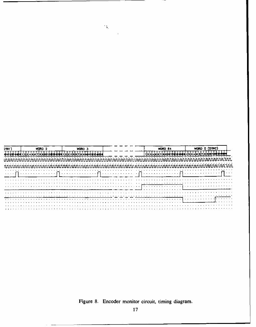
Figure 8, the timing diagram for the encoder monitor circuit, shows the waveforms ofthe signals and also the timing relationships among these signals. Each word of the mes-sage frame consists of 16 bits, with a word length of 768 pgs. The frequency of the "BITRATE CLOCK" signal is 20.8 kHz, and the bit period is 48 pgs. The rising or positive-going edge of this clock signal coincides with the start of each bit in the message frame.The frequency of the "WORD PULSE CLOCK" signal is 1.3 kHz, with a pulse width of48 pts. This pulse coincides in time with Bit 15 of each word in the message frame. The"FRAME SYNC" signal has a frequency of 20 Hz and a pulse width of 768 ps. Thenegative-going edge of the "FRAME SYNC" signal occurs 1-bit time before Word 0 Bit 0in the message frame. The "WORD COUNTER LOAD" signal has a pulse that occurs ata 20-Hz rate and has a pulse width of about 600 pgs.
DECODER MONITOR CIRCUIT
The decoder monitor circuit monitors tne Loral decoder data input signal. Figure 6 isalso the block diagram for this circuit. The major functional circuit blocks are the serial-to-parallel shift register, the word select timing circuit, and the storage register. The"NRZ DATA" input to the circuit is the "DELAYED NRZ" output signal from the LoralAPD-44A Decoder. The "WORD PULSE CLOCK" signal is the "WORD CLK" signaloutput from the Loral decoder. The "BIT RATE CLOCK" and the "FRAME SYNC"signals are also outputs from the decoder and are used by the monitor circuit to generatethe proper timing signals.
10

The serial-to-parallel shift register converts the serial "NRZ DATA" signal to 16 paral-lel data bits. These 16 bits are shifted through the register at the "BIT RATE CLOCK"frequency. The word select timing circuit generates the appropriate signals for selectingthe desired 16-bit word to be monitored. The inputs to this circuit are the "FRAMESYNC," "WORD PULSE CLOCK," "BIT RATE CLOCK," and "BCD WORD SELECT"signals. This circuit's output is the "WORD LOAD" signal that goes to the storage regis-ter. The storage register latches the selected 16-bit word, wben the appropriate pulseappears on the "WORD LOAD" signal.
CIRCUIT DESCRIPTION
The filowing paragraphs provide a detailed description of the decoder monitor cir-cuit. Figure 9 is the schematic drawing for this circuit.
U2 and U4 are two 8-bit serial shift registers combined to form a 16-bit serial-to-parallel shift register. The "DELAYED NRZ-L DATA" serial input goes to shift registerU4 (pin 1). The "BIT RATE CLOCK" signal goes to U2-8 and U4-8, the shift registerclock inputs. The combined 16 parallel outputs of U2 and U4 are the individual bits of the"NRZ-L DATA" signal being shifted at the "BIT RATE CLOCK" frequency.
The word select timing circuit consists of U6, U7, U8, U9, R3, C15, R5, and C17. The"FRAME SYNC" signal is connected to the RC network of R3 and C15 that filters outnoise on the incoming "FRAME SYNC" signal. This filtered "FRAME SYNC" signal goesto monostable multivibrator U6A. U6A generates a 600-gs pulse at the trailing ornegative-going edge of the "FRAME SYNC" pulse. The output of U6A (pin 4) is calledthe "WORD COUNTER LOAD" signal and is a negative-going pulse. This "WORDCOUNTER LOAD" signal is connected to the LOAD inputs of the synchronous BCDcounters U7 and U9. When a pulse is on the "WORD COUNTER LOAD" signal, theseven BCD word select inputs are loaded into U7 and U9 on the negative-going edge ofthe pulse. The "BCD WORD SELECT" inputs are the binary-coded decimal equivalent ofthe number N, the selected word being monitored. N can be any number between 0 and64.
R5 and C17 filter out noise from the incoming "WORD PULSE CLOCK" signal. Thisfiltered signal is NANDED with the "WORD COUNTER LOAD" signal. The output of theNAND gate, U8A-3, is applied to the down-count input of BCD counter U9 (pin 4). Eachtime a pulse appears on the "WORD PULSE CLOCK" signal, the combined BCD count ofU7 and U9 is decreased by 1 on the positive-going edge of the pulse. When N number ofthese pulses are counted by U7 and U9, the outputs of U7 and U9 will be "0." That is, theoutputs QA, QB, Qc, and QD shall all be "0" or in the low state. On the next pulse of the"WORD PULSE CLOCK" signal, a negative-going pulse is generated at the U7 BO output(pin 13). This BO output is called the "WORD LOAD" signal and is connected to theclock inputs (pin 11) of latches U3 and U5.
11

The "WORD LOAD" signal strobes the latches U3 and U5 at the appropriate time.That is, when the 16 data bits of the selected word (Word N in the message) are at theshift registers U2 and U4 outputs, the "WORD LOAD" pulse latches U3 and U5. Thislatching occurs on the positive-going edge of the "WORD LOAD" pulse. Thus, the U3and U5 outputs are the 16 bits of the selected word (Word N).
TIMING CIRCUIT
Figure 10 is the timing diagram for the decoder monitor circuit. It shows the signalwaveforms and the timing relationships among these signals. These signals are very simi-lar to those of the command monitor circuit. Each word of the message frame consists of16 bits, and the word length is 768 ps. The "BIT RATE CLOCK" signal frequency is 20.8kHz, and the bit period is 48 ps. The falling or negative-going edge of this clock signalcoincides with the start of each bit in the message frame. The "WORD PULSE CLOCK"signal frequency is 1.3 kHz, with a pulse width of 48 gs. This pulse coincides in time withBit 16 of each word in the message frame. The "FRAME SYNC" signal has a 20-Hzfrequency and a pulse width of 24 gs. The positive-going edge of the "FRAME SYNC"signal coincides with the start of Word 0 Bit 0 in the message frame. The "WORDCOUNTER LOAD" signal has a pulse that occurs at a 20-Hz rate, with a pulse width ofabout 600 jis.
12

EFFECTIVENESS OF CIRCUITS
ATV SYSTEM APPLICATION
Many operational hours were logged while developing and testing the ATV system.
During its initial checkout and throughout the system tests, the encoder monitor and de-coder monitor circuits have demonstrated their worth in detecting and troubleshootingproblems. In many cases, malfunctions were quickly isolated to the surface equipment orto the vehicle equipment by using these monitoring circuits. Thus, these circuits haveproven effective in decreasing the ATV system's mean time to repair (MTTR).
These monitor circuits were also utilized as a backup for monitoring signals that are
displayed to the operators. When a display or the circuit driving that display failed, themonitor circuit was used to select the specific signal that required monitoring. In addition,other signals not normally shown on dedicated displays can also be monitored using theseencoder and decoder monitor circuits.
OTHER APPLICATIONS
Besides using these monitor circuits with the Loral encoder and decoder units, these
circuits can be used to monitor other similar telemetry systems employing digitally multi-plexed data. However, the circuitry would probably have to be modified to match the dataor message format and the available timing signals of the particular telemetry system.
13

8
I1. LES OTHEMISE SPECIF IfA. ALL CAPACITO VALUES A,
* la [email protected]. -ALL RESSTOR VALUES AM,
* SO 1/4 WATT.2. REFEIiENCE AWINGS:
PRINTED I RIN B OARD: SSCIRCUIT CARD ASSEILY: SS5
UIC UlD
5437 5417
Ulf uIF
S487 S4117
U41
*Bv 6 .
S4CS
T.,,
SR
11 seiDIG Go 4
A6
M*4U
Tw-IB8

8 7 '- 5
. s °Sv
ALESS OTIUE SPECIID IU :* ALL CAPACITOR VALUES ARE IN MlICR. ORADS K UIA UleSIU 1Kmv . I"C AN S 2 ., _________________
* ALL RESISTOR VALUES ARE IN -HS COMMAND S ,S 1/4 WATT. DOWMNLINKFEArENCE DA INGS: (TELE
MtETRY
) SS - al 5497 5RINTED WIRINC BOARD: SS9Il-I2l1 IS2
IRCUIT CARD ASSEMBLY: SSS1-81257
COMMIAND 29(____ENCODER E/NRZ*L DATA 9- - . 2 1 _ lD _
54L 1;;4
BIT usRATE is p-------S. 8CLOCK U2A I SRC8
2R
54LSBO > c /-4IaSO - -
UC UID " D
S407 $487 9 4
___UIE UIF 1 " 2___ _ _ _----c
487 U3F 5497 7- S4LS164
4. 554LS221
7SACS -S5496 9 ~JR ~A
540IIST U SE 2 CA t EUSE
::
I~t 54LS164
17c, "I SV
.5VAA
R4 U7R .KU3A _4 LTRI C
-SV FRAME SYNC 17 --- - , TO>
Ll 7>iI i el _6V $rC I 441C 4IGA S4LS9SI6 C o o -7 TS isAC, .L 2P1, T *7 ,.2z r:-----X/CX.--' 2]I Bc" |.'
c __2_____ '21
7. 7_ 41 o 4152T I4.S192
L
us
4 R
CD WORD AS4PUL.SE 1s K1 >5U201DO1' %9CLOCKS4IS 9- IS
T 1s,, . - IIi2-V_ ____________
S4.S1S2
M1C4 4 I C.2 2 0 C1- 14O 1. C14 14~ i.Zs•j. 9.1 . " . u. Ju. , 91.1 ..:~~~~~ r 7 9 it 1i I• [m • ,
NEXT
7 6 46

DRAWINC NO. SHEET4 108179
I SHEET ' REV STATUS I REVIS. .S
REV , OF SHEETS ZONE t ZESCRI--:::.' :ATE A=PROVAJ
:OMMAN:2E
j11A ,
U4 rlie SIE 2'
1 I 5 406
14 ,IS::
IT 16 9NsT06 R
18 19 U IVE SIPN
RI2
17 16 it 1E
76 -- 9 S406 RIS
.3 .4L UI2B SI5 RV -T
, 14 ; 44120 510 -NT
!I I '" o8
128
' 115 1 !.1120/ 519 ANLr
2C S40
$ 6
+S 3 1? Ur. 12 ,S,._.IB.,
14Q 1 54056 RIS1 *NITORl
SS16 9 1 a a48 ANEL
540 R 1 1
S4LL7410 St '11
: I : 3
j 3E IR 3
:::,J. : IP1 } IV T
l 21 IS
PSISO
:2Si S4 :P
,34G
DII 2)15 --*U
NAVALOOCEAN.2.3 bLIT DO LD A DEGCA 925
DO OT CAESTISDRAIT
L -L I P 1 6
IITESSOTHRSE~ SPECFIE ORDEPA. PI R MNT'IE OI qTHE NAYPCR-.
DI ' ' .A NAA N
14 12
BREA ALRD
AT-V,/S oRSAX
AS , NEPE WNGL- IROEC NCCORDANCE SONAVA ____EAN___SYSTEMS ________ENTE_______
FIL N S SLECTIC
NET SS UEDON FE OUCdSSA NICIS APPROVED P 5 187
AP4I CATION RELEA DATE , T ORECT SCA OE SCHEMATIC ARA
= 4• Q- YN- , -R NO I ~'IZN I] S34IN NUMBERFC NrIR RWIGNr'1E
2t
:8 INTEXRE DRAWIN IN UCCRD E NAVA OCA YS TEMS CENTE8R 7A
APt.CTIN EEAEDgTE:D'!IEC; S A DE ONE CA 921S2:
DO~~~ NO SCAL THN AWN
Figure 7. Command monitor, schematic diagram.
tS~EAK ~ ~ l A.DGS -VE
:•2 C34 :MOV AL SHMA I ai in iAC A M m mmu I

WORD 64 I WORD 0 (SYNC) WORD 1 (SYNc) WORD 2
DATA 11467m G1 12457, -I- W444761 1346
SIT RATE CLOCK.nRUUUU~nuu
CLOCK n
..... . . .. .. ... ... .... ..I . .....I . .... .
;YJC= WORD 2 WORD 3 - - - - VMD64 I WORD 0(SVtC)411 1 4412134667J 4 12310 11 1 .6 11 12346760123467
lifa iUunri jjfjrujjiuinjuirn-u-
.... ... ... ... ... ... ... ...Figure... ..8. Encoder.monitor.circuit,.timing.diagram.. . ... .. .. .. n .. .. .. .. ..n - - n .. .. .. .. ..n .. .. .. ...1--

8 6
I. -U LE OTt" 1I1 SICIFIO : SvA. ALL CAPACITO VALLS ARE IN lCROARADS
! log umivlac. R2I9. ALL SImSTOR VALM AIM IN % IK UiA UIB 1K" S S /4 ATT.
2 32. RE MtnN E M A I GS~5 : INST M S (SS I I
PRINTED WINING BOARD: 55 "1U-U91316f PLI54CIROJIT CARD ASSEMBLY: 6SXI-'12316S (DECODER) 56 p,1 Ci
46 /.INSTr ' Pi
-LILw 47 PI R I
C1/-4
I _D
12
1, 1!3
S4LS164
U4
I SRC8BIT RATE CLOCK 19 I
DELAYED 38 pi .- moNRZ-L
DATA i9 P
6 -..
IL
12
54LS164
.5v
UAR4 LU7B
R3 SK US 4 CTRD1VIOTSV FRAME SYNC 17a I UP :
LI I A 1 4D
. . .. ........ ,....IL..._.4c_,LOAD
.B 6 Pi I VK29210-39 26Dv 14.. *---KCx 3 ALQ-D
Il II v4LS221 I=23= 1c
;:~ ~ s :sL I
I. 14CTIDIVIB
CD ~ DIUA 2ns
PLILSE lB p 2LDIG GND 4 Pij----. CLOCK P1 14 S201LOA
S&5 152.SV
IC4S- 47 IC7 IC4 7U7 S",C R1 IS '4~ C.L 12ui -7 -i WT'i C4 ~ T'] IW TC7 9 1~ U. Cie 1 C1 2J2
80 1 6 5Z 0.1

I DRAWJING NO I SHEET
OV SHEET S O R E IIONS AT~~E V RE TTS~,PRVA..
!2K
P. 26 INSTMIJPLIN'
U ISAR6
2
54U6 I0 Sir ~ ;2
____ __ 5406 SI9
12 2 S E S4 RIE
14 1 . v 5 SRP
9 >23
54L3 7 12 UIO r? 611 '
4IS5406 RIC
71 12 - j 24IS 5406 LI1IS SIO P
.2" 43 612R256
UIA 5406 10 P
12110 516 , )265406 RIS SI
11 4
7 - ' 6S440
14 14
S4L2S 64 289
540 SIB SI P1 _
C ~5406 Rl
3~. 2 CSA 6D U I
U S4LSIB
m~1I 543 l~I ~ 15j0y
CTI14I SE2 C 54L526
54L37 4 7 54L50
.R - PI S4 -j
12 s U12EYR~ _____________________________________________________________________ PRTSC7
2t U10 isT DO T 0DO: NOT SC IIIS -RwN SAL DEO A 92-
AREA LEG I AUP12VE 12 10Tu N A:~
us BCD WORD O '4lFACE1 oUED s AIRCE NO DUS-D- S4LS22
APPIVl ELCTIO a 54LASE DAT 1 9 2RET SAE OGS"E
4I 33 2l150
Fi ue 9 ntu enai n m ntr sh m tc dar m

WRD 64 Z WORD 0 (SYNC) =VRm I (SYNC)DATA 2'3456-1.S stA 44- ,246S I- 123466 i - 31-41
CILOTCLOC
LO
I . .. . . . . . . . . . . . . . . . . . . . . . ... . . . .

ORD I(SYNC) I WORD 2 WORD 3WR 4WOD0(YC
n :::: n,
. ........ ...... ...... .... ..... .... ...... ...... ... ... ..... .... .... .......: : : : : : : t : :
Figure 10. Decoder monitor circuit, timing diagram.
21

REPORT DOCUMENTATION PAGE Form ApprovedI OMB No. 0704-0188
Public reporting burden for this cotlection of Information Is stlmaled to average 1 hour per response. Including the time for reviewing instructions, searching existing data sources gathering andmaintaining the data needed, and completing and reviewing the ooectlon of Information Send comments regarding this burden estimate or any other aspect of this collection of Information. Includingsuggestions for reducing this burden. to Washington Headquarters Services. Directorate for Information Operations and Reports. 1215 Jefferson Davis Hig hway. Suite 1204. Arlington. VA 22202-4302and to the Office of Management and Budget. Papenwork Reduction Projec (0704-0188). Washington. DC 20503.
1. AGENCY USE ONLY (Leave bla,,,'t 2 REPORT DATE 3. REPORT TYPE AND DATES COVERED
July 1991 Final: Jan 1991-May 1991
4 'r E AND SUBTTtLE 5. FUNDING NUMBERS
, ENCODER AND DECODER MONITOR CIRCUITS PE: 603713NPROJ: MS09WU: DN188 508
6. AUTHOR(S)
C. A. Kunitaka, W. S. Morinaga, and K. Perreira
7. PERFORMING ORGANIZATION NAME(S) AND ADDRESS(ES) 8. PERFORMING ORGANIZATIONREPORT NUMBER
Naval Ocean Systems CenterSan Diego, CA 92152-5000 :'OSC TR 1439
9. SPONSORING/MONITORING AGENCY NAME(S) AND ADDRESS(ES) 10 SPONSORING/MONITORINGAGENCY REPORT NUMBER
Naval Sea Systems CommandWashington, DC 20362
11 SUPPLEMENTARY NOTES
12a DISTRIBUTION/AVAILAILTY STATEMENT 12b. DISTRIBUTION CODE
Approved for public release; distribution is unlimited.
13 ABSTRACT (Maximum 200 words)
This report describes the telemetry monitoring circuits employed in the Advanced Tethered Vehicle (ATV) system-a remotely con-trolled submersible vehicle. These circuits are used to monitor the telemetered commands and data that are transmitted between thesurface and the submersible. They provide online monitoring of the individual bits in the serial digital-data stream. The report providesa detailed description of the design and operation of these circuits.
t4 SUBJECT TERMS t5 NUMBER OF PAGES
2516 PRICE CODE
17 SECURITY CLASSIFICATION 18 SECURITY CLASSIFICATION 19 SECURITY CLASSIFICATION 20 UMITATION OF ABSTRACTOF REPORT OF THIS PAGE OF ABSTRACT
UNCLASSIFIED UNCLASSIFIED UNCLASSIFIED SAME AS REPORT
NSN 7540-01 -280-5500 Standard form 29

21 & NAME OF RESPONSIBLE INDIMiUAL 21b. TELEPHONE (IclWeOlAMCode) 21c. OFFICE SYMBOL
W. S. Morinaga (808) 257-5289 Code 534
NSN 754001-2804600 Stndard Poem 2M8

INITIAL DISTRIBUTION
Code 0012 Patent Counsel (1)
Code 0144 R. November (1)
Code 532H Robert Hoffman (20)
Code 534H Wayne Morinaga (30)Code 534H Chun Hui (2)
Code 534H Gary Redman (2)
Code 942 Robert Bixler (5)
Code 952B J. Puleo (1)Code 961 Archive/Stock (6)Code 964B Library (3)
Defense Technical Information Center
Alexandria, VA 22304-6145 (4)
NOSC Liaison OfficeWashington, DC 20363-5100 (1)
Center for Naval AnalysesAlexandria, VA 22302-0268 (1)
Navy Acquisition, Research & Develop-
ment Information Center (NARDIC)
Alexandria, VA 22333 (1)
Naval Sea Systems Command
Washington, DC 20362-5101 (5)
Navy Public Works CenterPearl Harbor, HI 96860 (5)
II


![· 061uec1B03HaHne: CM01UffMHa A-ITHHa I I crracc npH3ep, 1-fflCTaBH1ffx.-: 0.1]. BepryH0Ba Aapbfl 8 Kiracc — npwep, 1-racT'dBF-ff11](https://img.dokumen.tips/doc/110x75/5ad368767f8b9a05208deeaf/cm01uffmha-a-ithha-i-i-crracc-nph3ep-1-fflctabh1ffx-01-bepryh0ba-aapbfl-8.jpg)


