Embed Size (px)
Citation preview
Microelectronic Circuits, Seventh Edition Sedra/Smith Copyright © 2015 by Oxford University Press
CHAPTER 11
Feedback
Microelectronic Circuits, Seventh Edition Sedra/Smith Copyright © 2015 by Oxford University Press
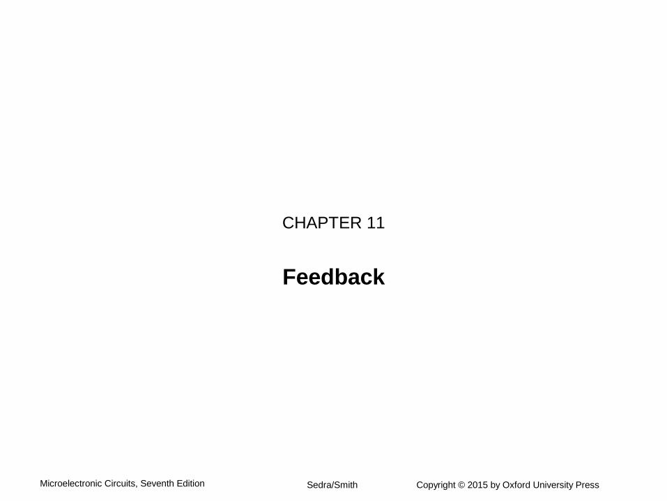
Figure 11.1 General structure of the feedback amplifier. This is a signal-flow diagram, and the
quantities x represent either voltage or current signals.
Microelectronic Circuits, Seventh Edition Sedra/Smith Copyright © 2015 by Oxford University Press
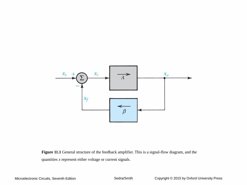
Figure 11.2 Determining the loop gain by breaking the feedback loop at the output of the basic amplifier,
applying a test signal xt, and measuring the returned signal xr : Aβ ≡ −xr/xt.
Microelectronic Circuits, Seventh Edition Sedra/Smith Copyright © 2015 by Oxford University Press
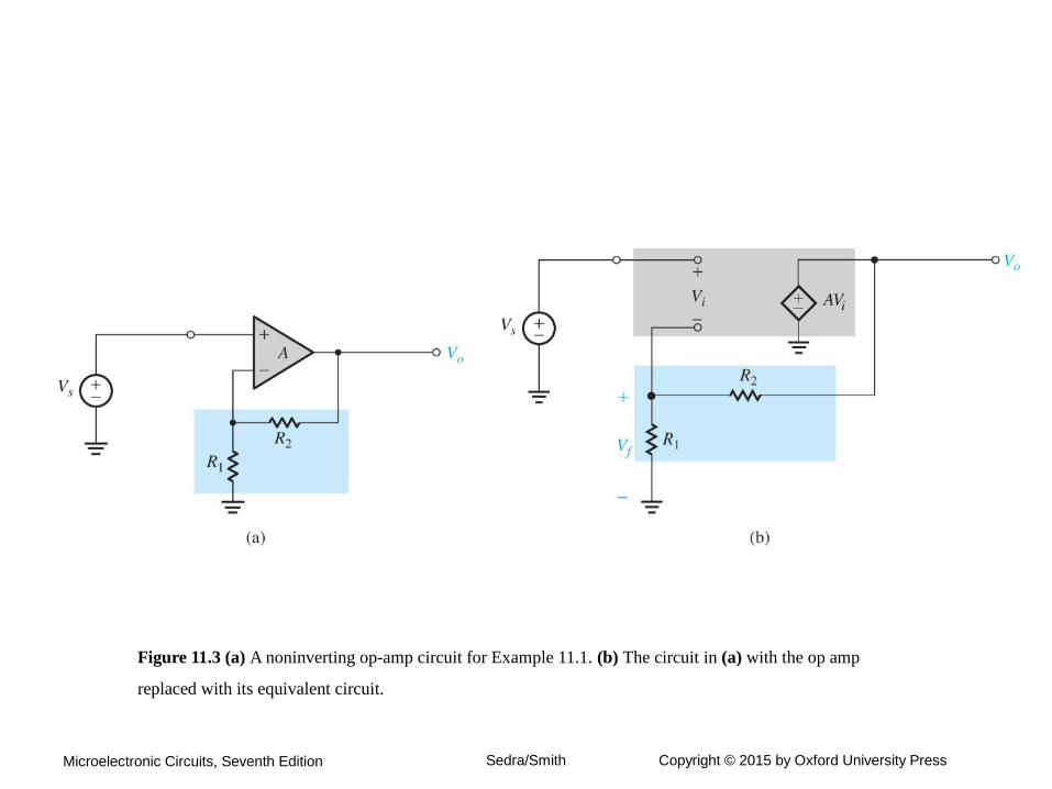
Figure 11.3 (a) A noninverting op-amp circuit for Example 11.1. (b) The circuit in (a) with the op amp
replaced with its equivalent circuit.
Microelectronic Circuits, Seventh Edition Sedra/Smith Copyright © 2015 by Oxford University Press
Microelectronic Circuits, Seventh Edition Sedra/Smith Copyright © 2015 by Oxford University Press
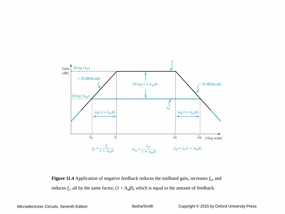
Figure 11.4 Application of negative feedback reduces the midband gain, increases fH, and
reduces fL, all by the same factor, (1 + AMβ), which is equal to the amount of feedback.
Microelectronic Circuits, Seventh Edition Sedra/Smith Copyright © 2015 by Oxford University Press
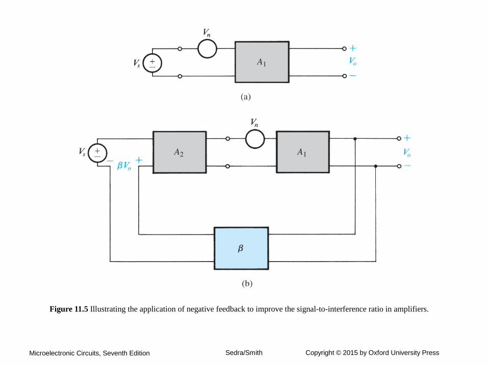
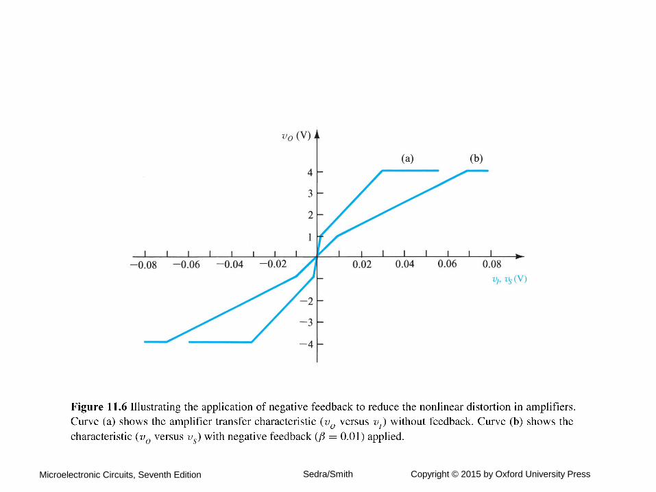
Figure 11.5 Illustrating the application of negative feedback to improve the signal-to-interference ratio in amplifiers.
Microelectronic Circuits, Seventh Edition Sedra/Smith Copyright © 2015 by Oxford University Press
Microelectronic Circuits, Seventh Edition Sedra/Smith Copyright © 2015 by Oxford University Press
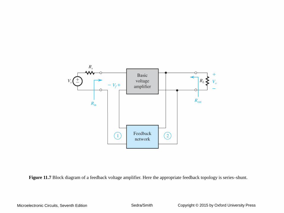
Figure 11.7 Block diagram of a feedback voltage amplifier. Here the appropriate feedback topology is series–shunt.
Microelectronic Circuits, Seventh Edition Sedra/Smith Copyright © 2015 by Oxford University Press
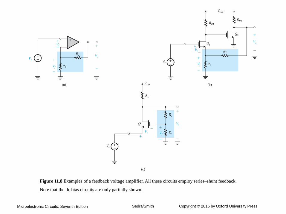
Figure 11.8 Examples of a feedback voltage amplifier. All these circuits employ series–shunt feedback.
Note that the dc bias circuits are only partially shown.
Microelectronic Circuits, Seventh Edition Sedra/Smith Copyright © 2015 by Oxford University Press
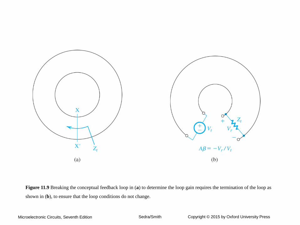
Figure 11.9 Breaking the conceptual feedback loop in (a) to determine the loop gain requires the termination of the loop as
shown in (b), to ensure that the loop conditions do not change.
Microelectronic Circuits, Seventh Edition Sedra/Smith Copyright © 2015 by Oxford University Press
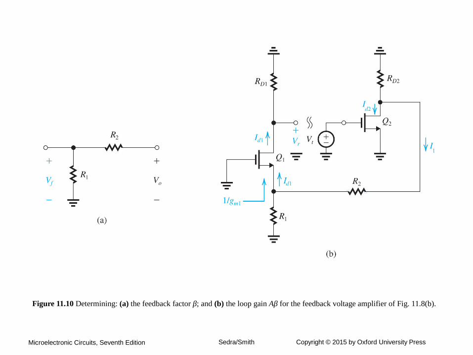
Figure 11.10 Determining: (a) the feedback factor β; and (b) the loop gain Aβ for the feedback voltage amplifier of Fig. 11.8(b).

Microelectronic Circuits, Seventh Edition Sedra/Smith Copyright © 2015 by Oxford University Press
Figure 11.11 Example 11.3. (a) A series–shunt feedback amplifier; (b) the feedback loop obtained by setting Vs = 0 and
replacing the op amp with its equivalent-circuit model; (c) breaking the feedback loop to determine the loop gain Aβ = −Vr/Vt.
Microelectronic Circuits, Seventh Edition Sedra/Smith Copyright © 2015 by Oxford University Press
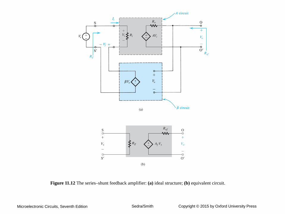
Figure 11.12 The series–shunt feedback amplifier: (a) ideal structure; (b) equivalent circuit.
Microelectronic Circuits, Seventh Edition Sedra/Smith Copyright © 2015 by Oxford University Press
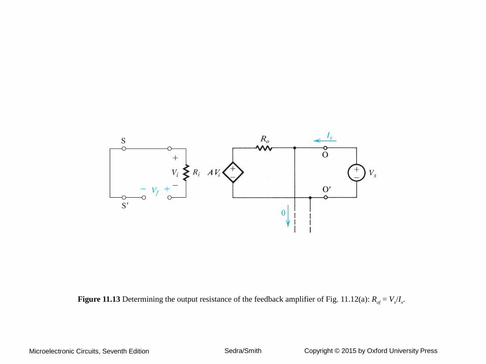
Figure 11.13 Determining the output resistance of the feedback amplifier of Fig. 11.12(a): Rof = Vx/Ix.

Microelectronic Circuits, Seventh Edition Sedra/Smith Copyright © 2015 by Oxford University Press
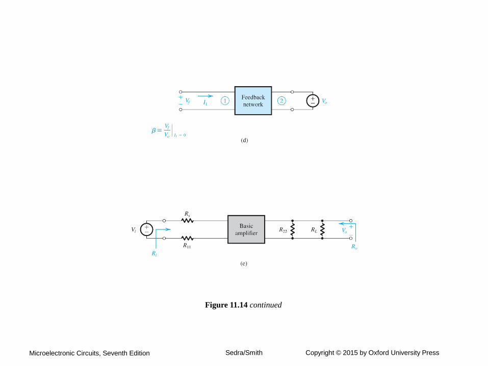
Figure 11.14 (a) Block diagram of a practical series–shunt feedback amplifier. (b) The circuit in (a)
represented by the ideal structure of Fig. 11.12(a). (c) Definition of R11 and R22. (d) Determination of
the feedback factor β. (e) The A circuit, showing the open-loop resistances Ri and Ro.
Microelectronic Circuits, Seventh Edition Sedra/Smith Copyright © 2015 by Oxford University Press
Figure 11.14 continued
Microelectronic Circuits, Seventh Edition Sedra/Smith Copyright © 2015 by Oxford University Press
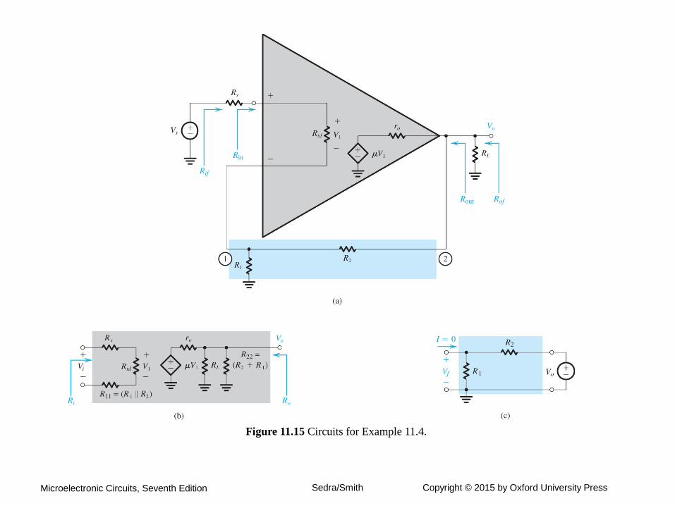
Figure 11.15 Circuits for Example 11.4.

Microelectronic Circuits, Seventh Edition Sedra/Smith Copyright © 2015 by Oxford University Press
Figure 11.16 (a) Series–shunt feedback amplifier for Example 11.5; (b) the A circuit; (c) the β circuit.
Microelectronic Circuits, Seventh Edition Sedra/Smith Copyright © 2015 by Oxford University Press
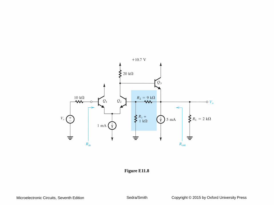
Figure E11.8

Microelectronic Circuits, Seventh Edition Sedra/Smith Copyright © 2015 by Oxford University Press
Figure 11.17 Example 11.6.

Microelectronic Circuits, Seventh Edition Sedra/Smith Copyright © 2015 by Oxford University Press
Figure 11.18 The feedback transconductance amplifier (series–series).
Microelectronic Circuits, Seventh Edition Sedra/Smith Copyright © 2015 by Oxford University Press
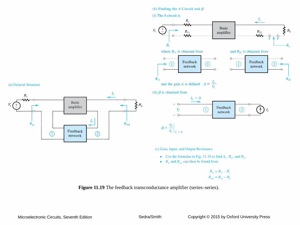
Figure 11.19 The feedback transconductance amplifier (series–series).
Microelectronic Circuits, Seventh Edition Sedra/Smith Copyright © 2015 by Oxford University Press
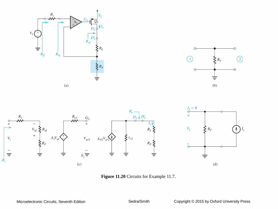
Figure 11.20 Circuits for Example 11.7.
Microelectronic Circuits, Seventh Edition Sedra/Smith Copyright © 2015 by Oxford University Press
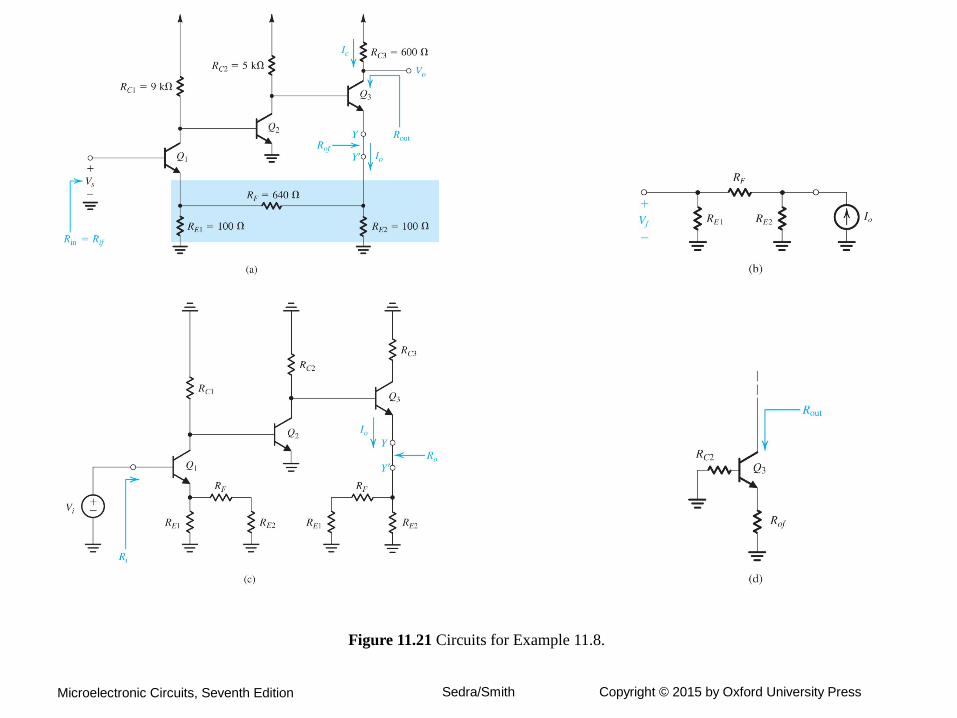
Figure 11.21 Circuits for Example 11.8.
Microelectronic Circuits, Seventh Edition Sedra/Smith Copyright © 2015 by Oxford University Press
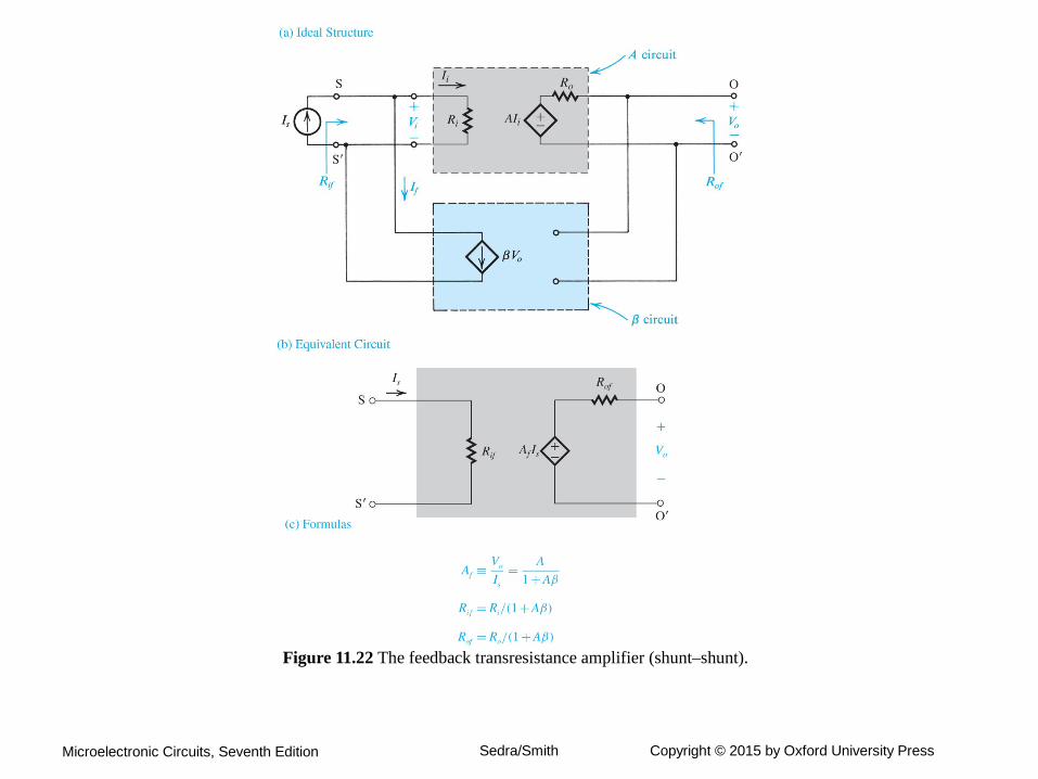
Figure 11.22 The feedback transresistance amplifier (shunt–shunt).
Microelectronic Circuits, Seventh Edition Sedra/Smith Copyright © 2015 by Oxford University Press
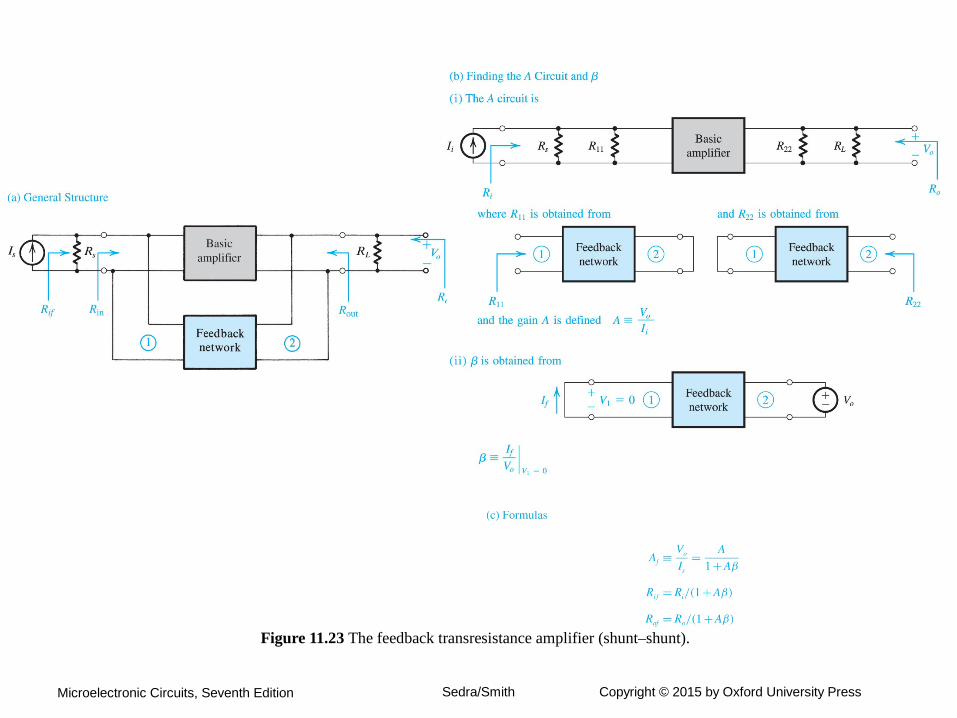
Figure 11.23 The feedback transresistance amplifier (shunt–shunt).
Microelectronic Circuits, Seventh Edition Sedra/Smith Copyright © 2015 by Oxford University Press
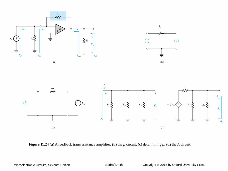
Figure 11.24 (a) A feedback transresistance amplifier; (b) the β circuit; (c) determining β; (d) the A circuit.

Microelectronic Circuits, Seventh Edition Sedra/Smith Copyright © 2015 by Oxford University Press
Figure E11.19
Microelectronic Circuits, Seventh Edition Sedra/Smith Copyright © 2015 by Oxford University Press
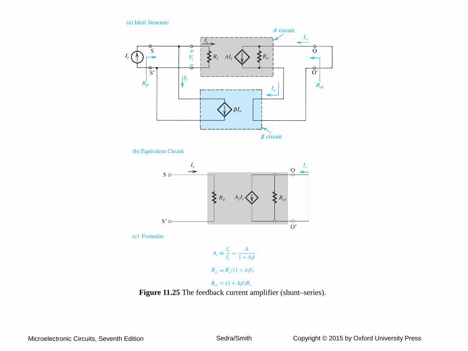
Figure 11.25 The feedback current amplifier (shunt–series).
Microelectronic Circuits, Seventh Edition Sedra/Smith Copyright © 2015 by Oxford University Press
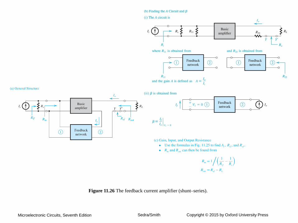
Figure 11.26 The feedback current amplifier (shunt–series).
Microelectronic Circuits, Seventh Edition Sedra/Smith Copyright © 2015 by Oxford University Press
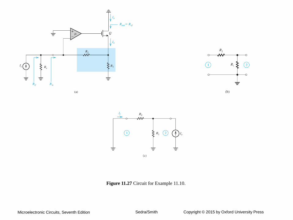
Figure 11.27 Circuit for Example 11.10.
Microelectronic Circuits, Seventh Edition Sedra/Smith Copyright © 2015 by Oxford University Press
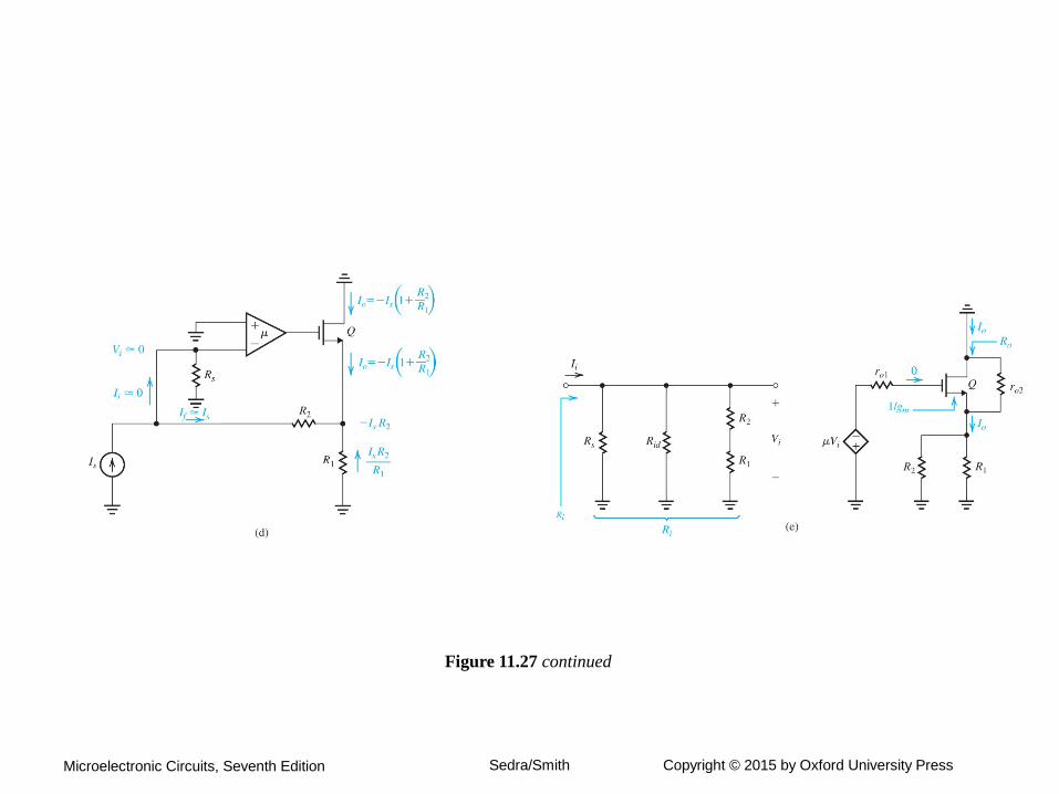
Figure 11.27 continued
Microelectronic Circuits, Seventh Edition Sedra/Smith Copyright © 2015 by Oxford University Press
Microelectronic Circuits, Seventh Edition Sedra/Smith Copyright © 2015 by Oxford University Press
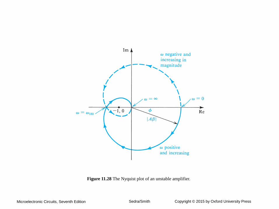
Figure 11.28 The Nyquist plot of an unstable amplifier.
Microelectronic Circuits, Seventh Edition Sedra/Smith Copyright © 2015 by Oxford University Press
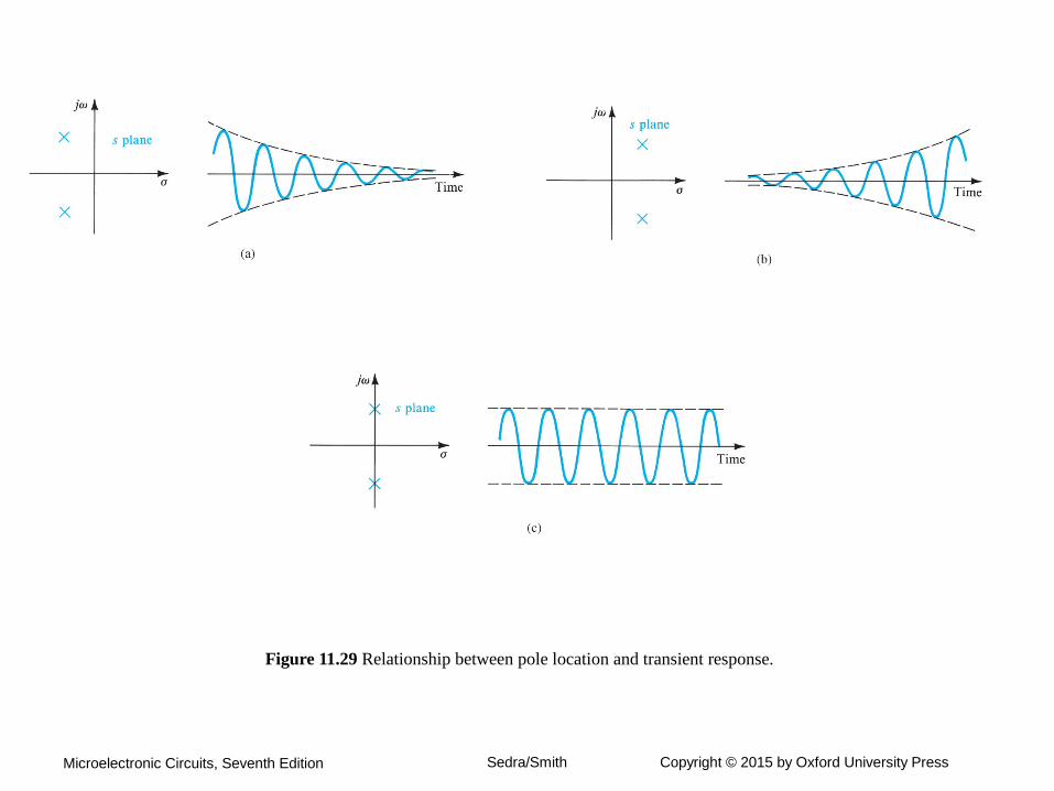
Figure 11.29 Relationship between pole location and transient response.
Microelectronic Circuits, Seventh Edition Sedra/Smith Copyright © 2015 by Oxford University Press
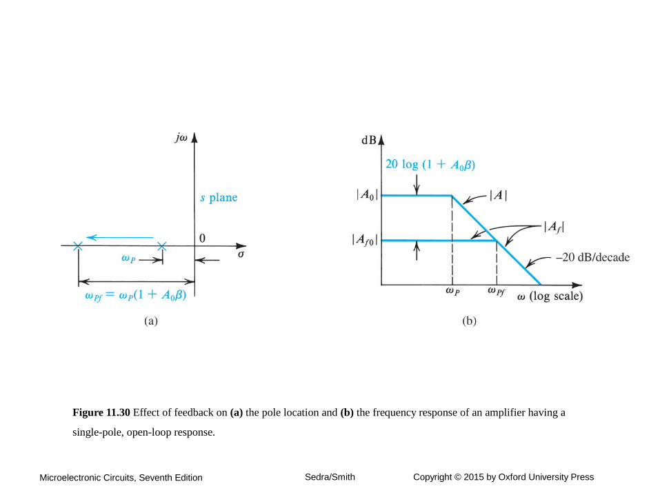
Figure 11.30 Effect of feedback on (a) the pole location and (b) the frequency response of an amplifier having a
single-pole, open-loop response.
Microelectronic Circuits, Seventh Edition Sedra/Smith Copyright © 2015 by Oxford University Press
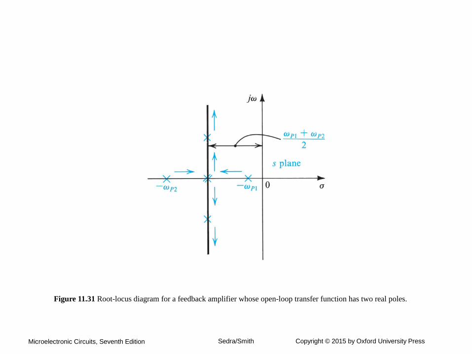
Figure 11.31 Root-locus diagram for a feedback amplifier whose open-loop transfer function has two real poles.
Microelectronic Circuits, Seventh Edition Sedra/Smith Copyright © 2015 by Oxford University Press
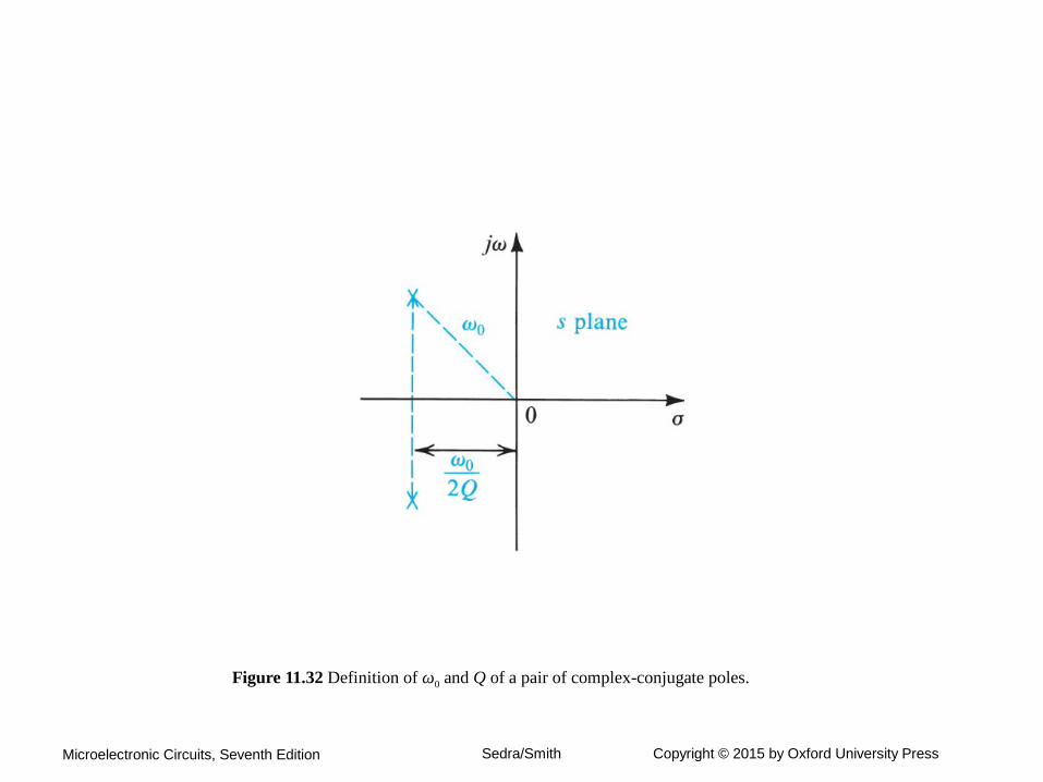
Figure 11.32 Definition of ω0 and Q of a pair of complex-conjugate poles.
Microelectronic Circuits, Seventh Edition Sedra/Smith Copyright © 2015 by Oxford University Press
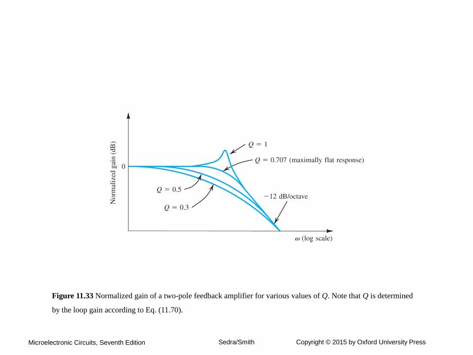
Figure 11.33 Normalized gain of a two-pole feedback amplifier for various values of Q. Note that Q is determined
by the loop gain according to Eq. (11.70).
Microelectronic Circuits, Seventh Edition Sedra/Smith Copyright © 2015 by Oxford University Press
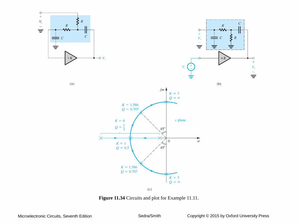
Figure 11.34 Circuits and plot for Example 11.11.
Microelectronic Circuits, Seventh Edition Sedra/Smith Copyright © 2015 by Oxford University Press
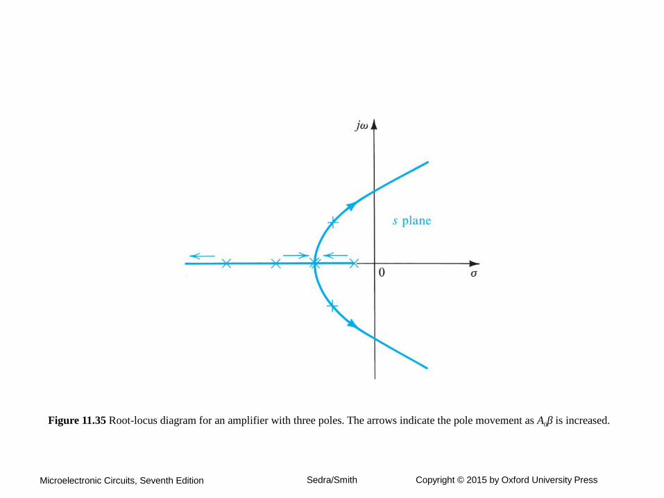
Figure 11.35 Root-locus diagram for an amplifier with three poles. The arrows indicate the pole movement as A0β is increased.

Microelectronic Circuits, Seventh Edition Sedra/Smith Copyright © 2015 by Oxford University Press
Figure E11.26
Microelectronic Circuits, Seventh Edition Sedra/Smith Copyright © 2015 by Oxford University Press
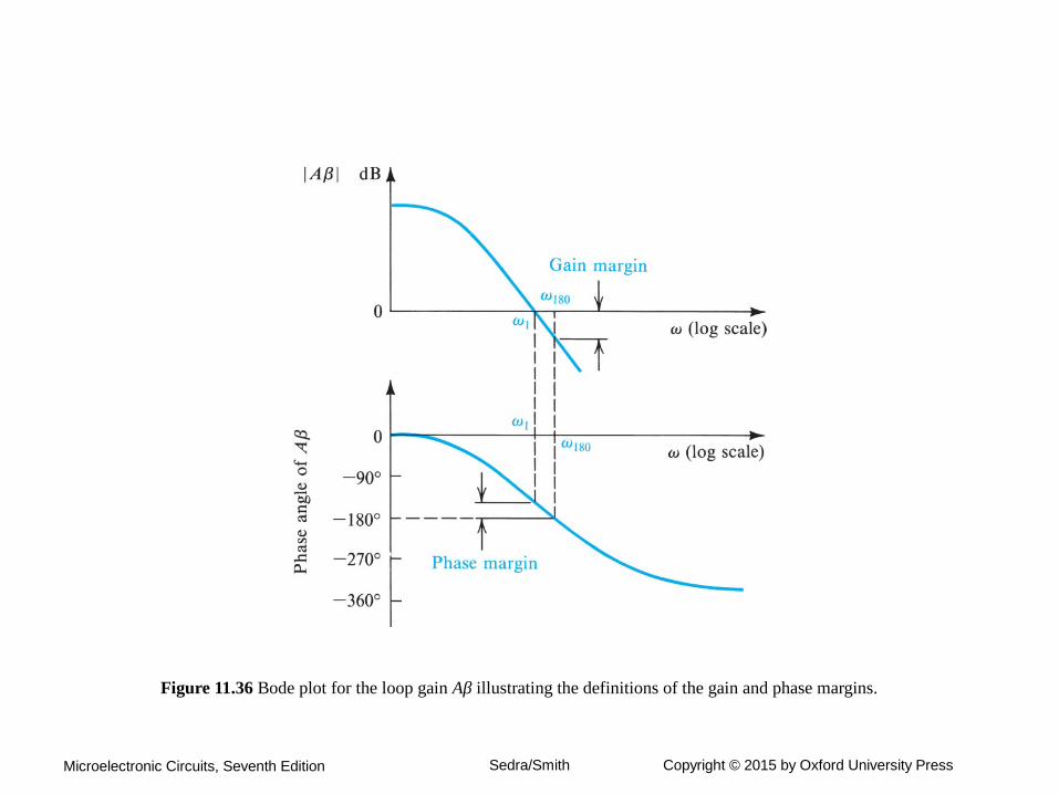
Figure 11.36 Bode plot for the loop gain Aβ illustrating the definitions of the gain and phase margins.
Microelectronic Circuits, Seventh Edition Sedra/Smith Copyright © 2015 by Oxford University Press
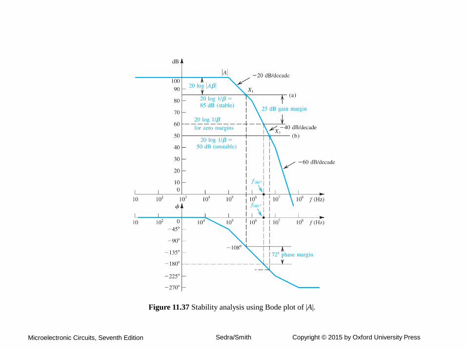
Figure 11.37 Stability analysis using Bode plot of |A|.
Microelectronic Circuits, Seventh Edition Sedra/Smith Copyright © 2015 by Oxford University Press
Microelectronic Circuits, Seventh Edition Sedra/Smith Copyright © 2015 by Oxford University Press
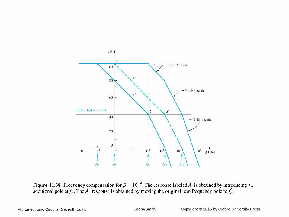
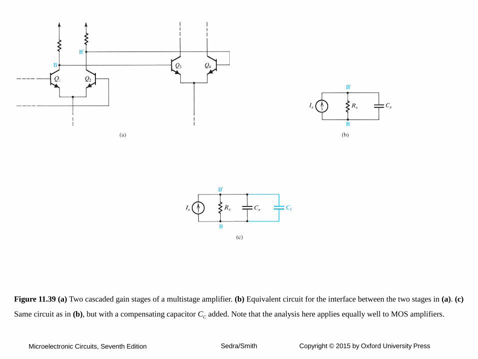
Figure 11.39 (a) Two cascaded gain stages of a multistage amplifier. (b) Equivalent circuit for the interface between the two stages in (a). (c)
Same circuit as in (b), but with a compensating capacitor CC added. Note that the analysis here applies equally well to MOS amplifiers.
Microelectronic Circuits, Seventh Edition Sedra/Smith Copyright © 2015 by Oxford University Press
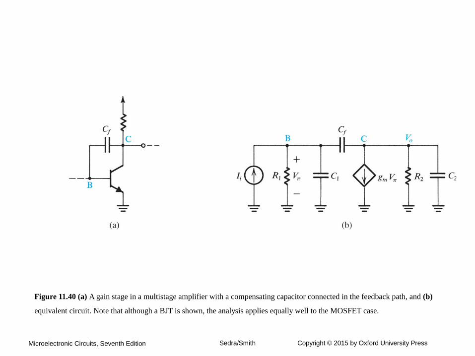
Figure 11.40 (a) A gain stage in a multistage amplifier with a compensating capacitor connected in the feedback path, and (b)
equivalent circuit. Note that although a BJT is shown, the analysis applies equally well to the MOSFET case.
Microelectronic Circuits, Seventh Edition Sedra/Smith Copyright © 2015 by Oxford University Press
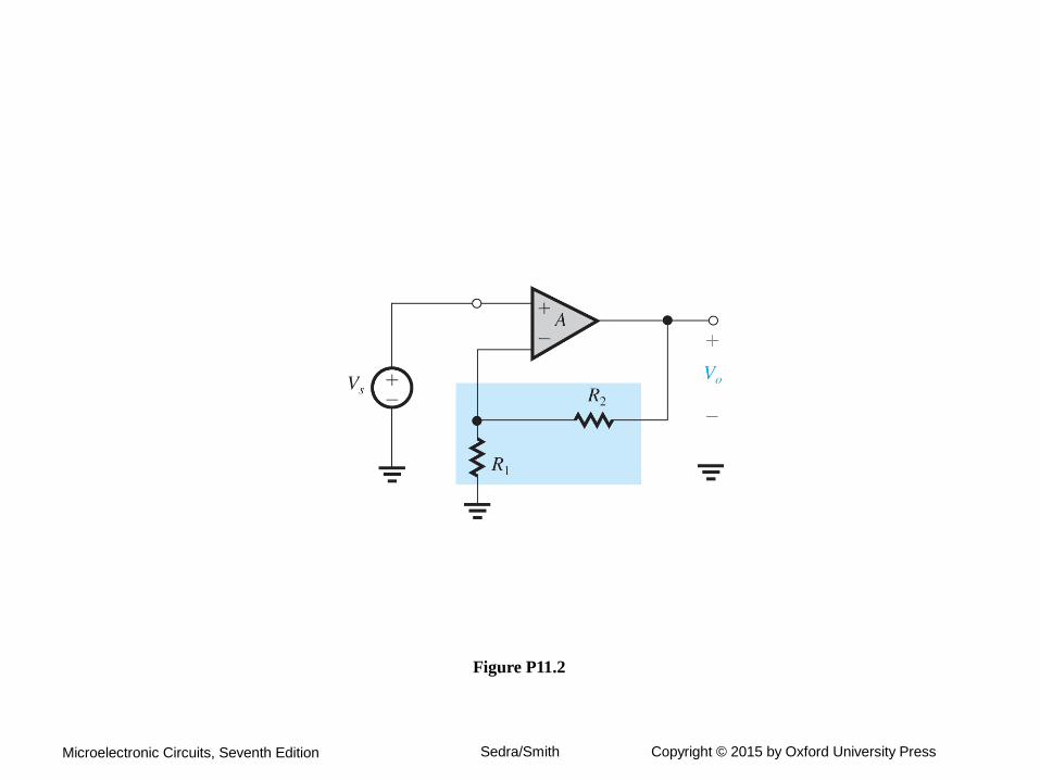
Figure P11.2
Microelectronic Circuits, Seventh Edition Sedra/Smith Copyright © 2015 by Oxford University Press
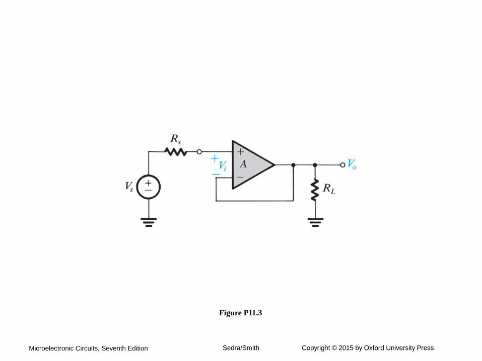
Figure P11.3
Microelectronic Circuits, Seventh Edition Sedra/Smith Copyright © 2015 by Oxford University Press
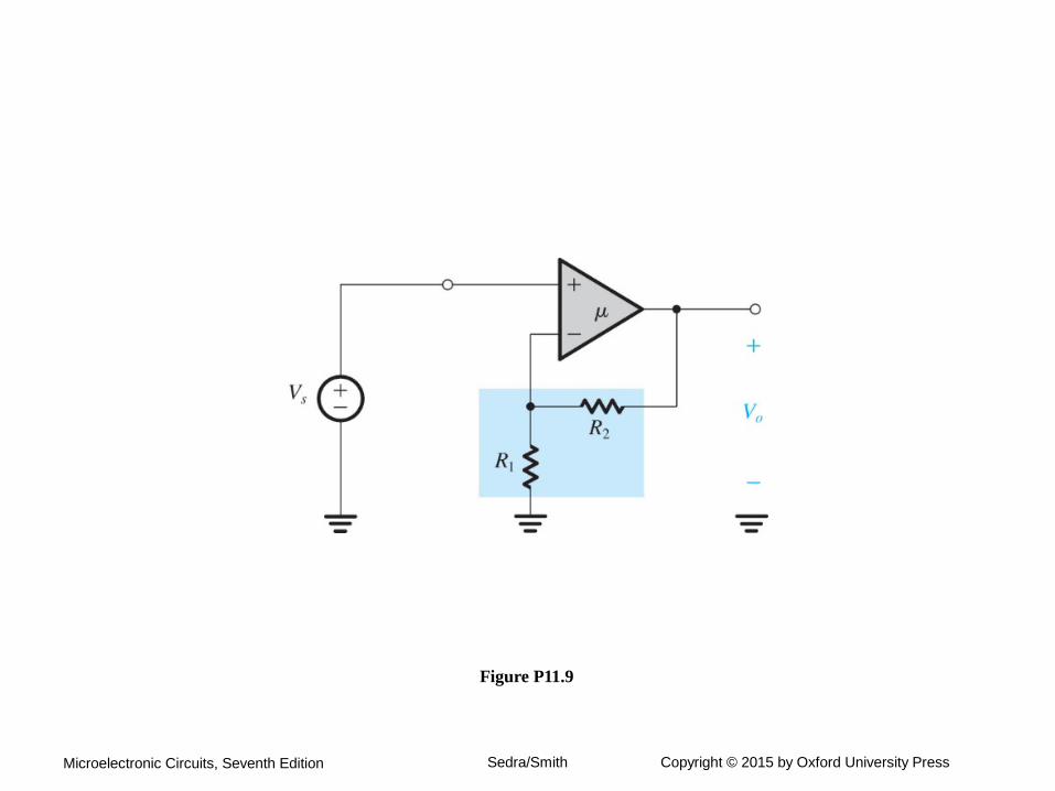
Figure P11.9
Microelectronic Circuits, Seventh Edition Sedra/Smith Copyright © 2015 by Oxford University Press
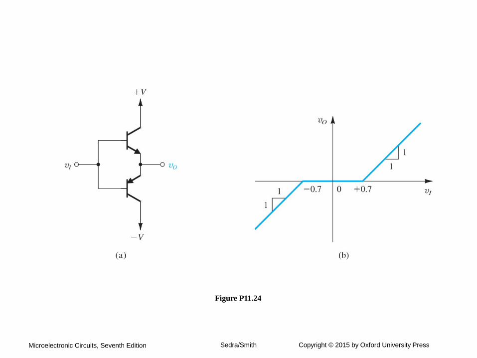
Figure P11.24
Microelectronic Circuits, Seventh Edition Sedra/Smith Copyright © 2015 by Oxford University Press
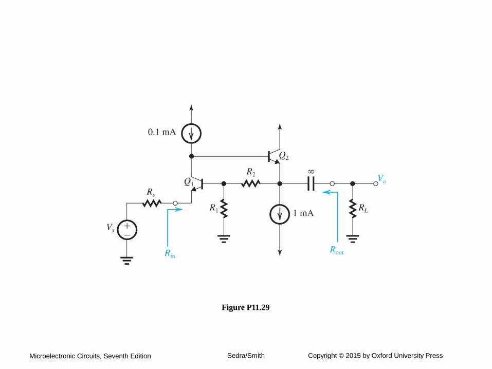
Figure P11.29
Microelectronic Circuits, Seventh Edition Sedra/Smith Copyright © 2015 by Oxford University Press
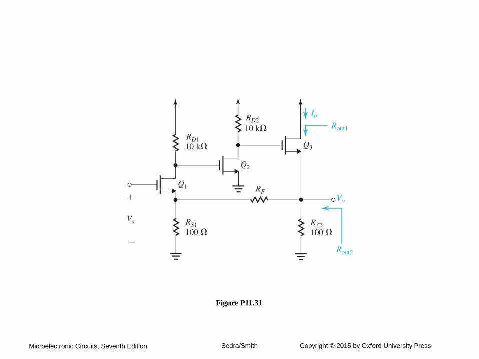
Figure P11.31
Microelectronic Circuits, Seventh Edition Sedra/Smith Copyright © 2015 by Oxford University Press
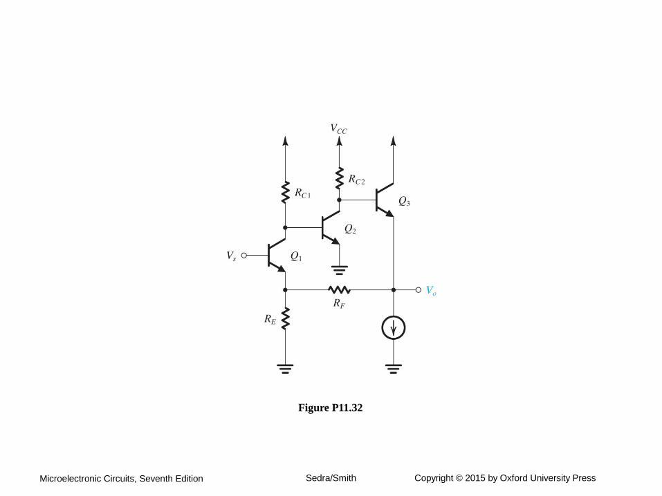
Figure P11.32
Microelectronic Circuits, Seventh Edition Sedra/Smith Copyright © 2015 by Oxford University Press
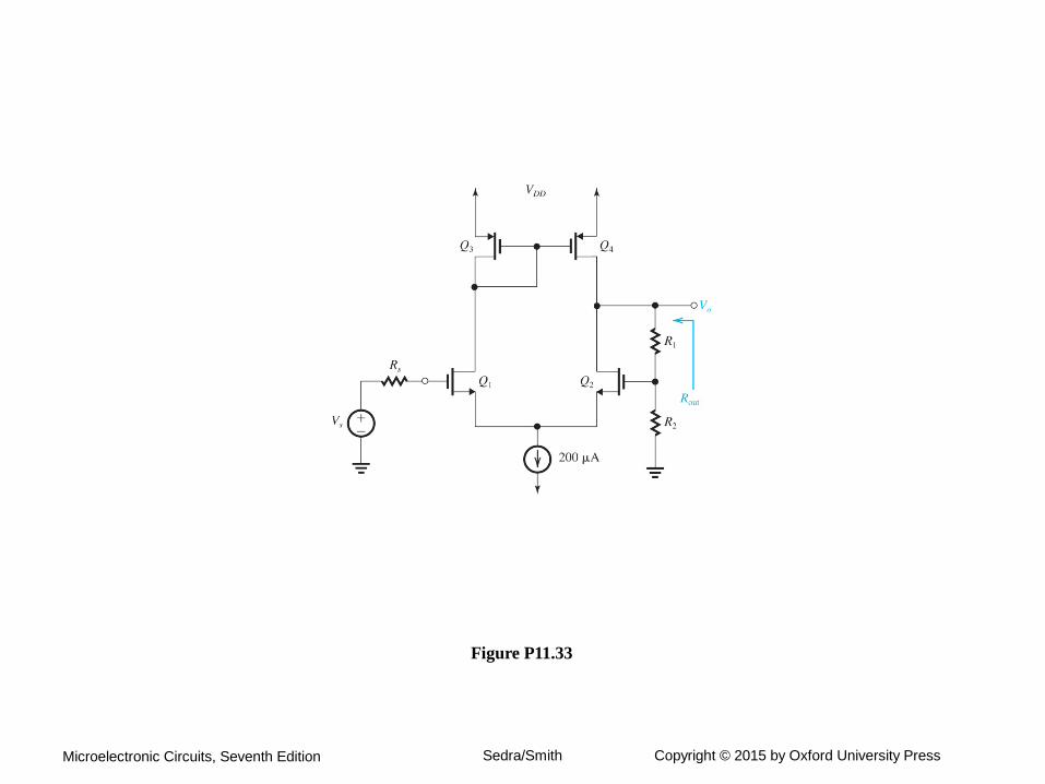
Figure P11.33
Microelectronic Circuits, Seventh Edition Sedra/Smith Copyright © 2015 by Oxford University Press
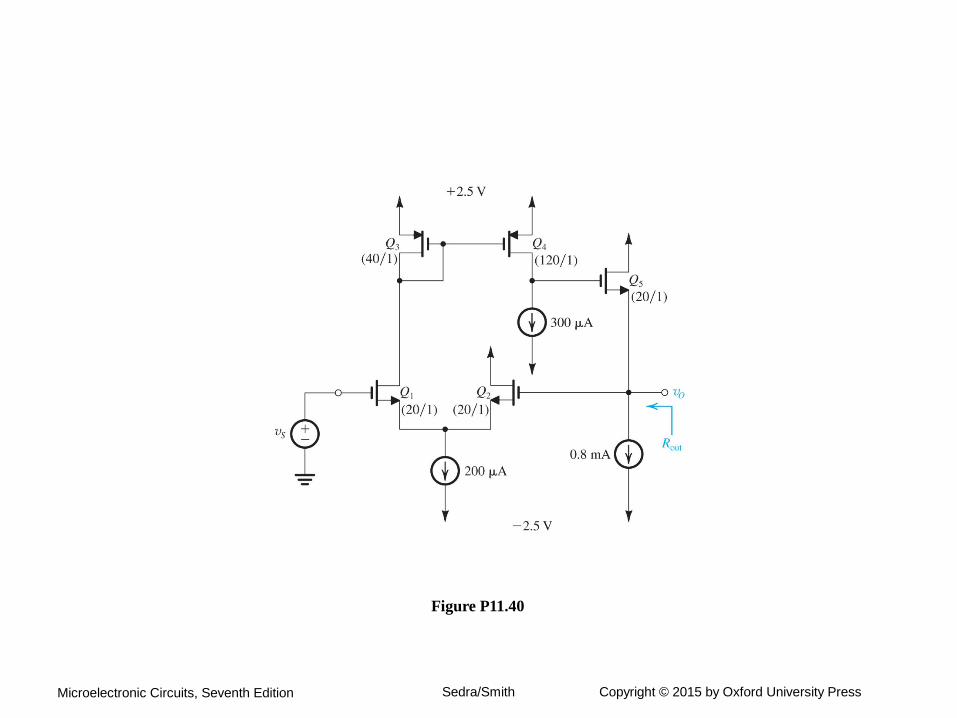
Figure P11.40
Microelectronic Circuits, Seventh Edition Sedra/Smith Copyright © 2015 by Oxford University Press
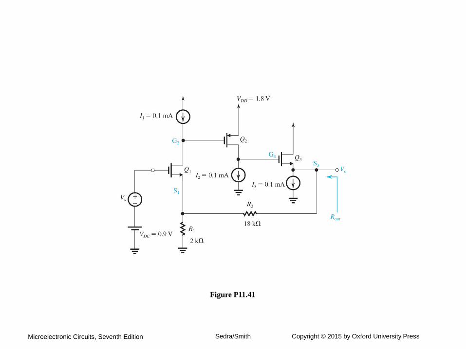
Figure P11.41
Microelectronic Circuits, Seventh Edition Sedra/Smith Copyright © 2015 by Oxford University Press
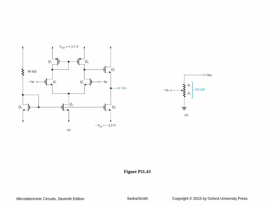
Figure P11.43
Microelectronic Circuits, Seventh Edition Sedra/Smith Copyright © 2015 by Oxford University Press
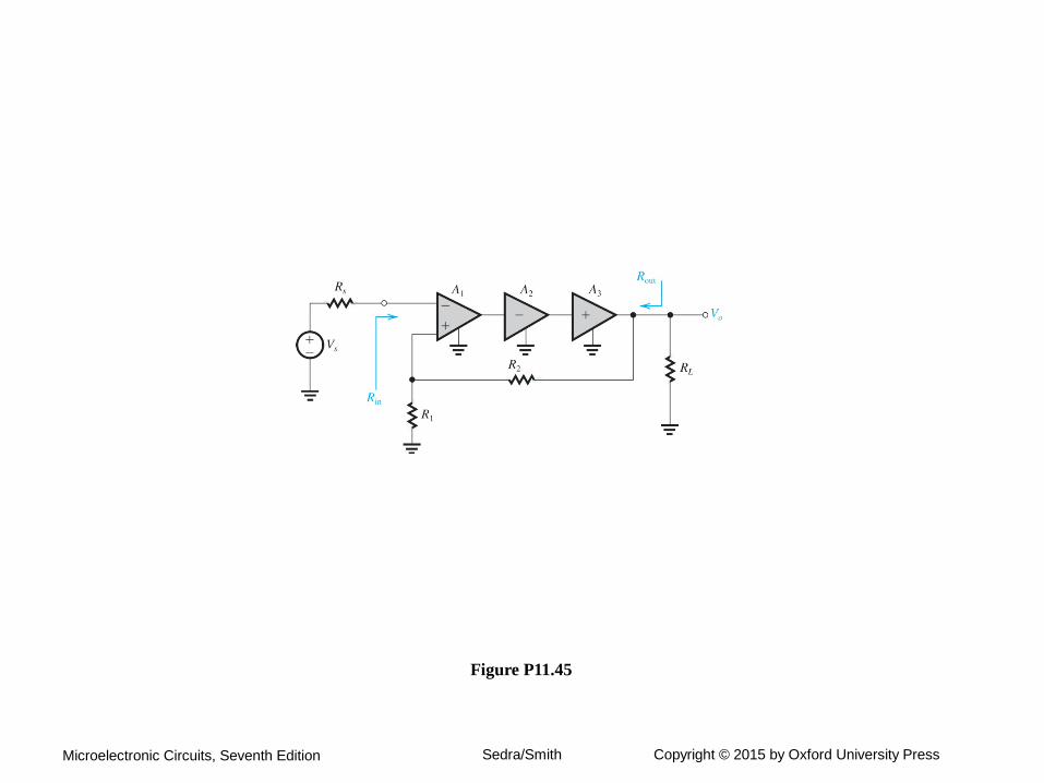
Figure P11.45
Microelectronic Circuits, Seventh Edition Sedra/Smith Copyright © 2015 by Oxford University Press
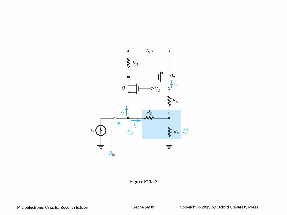
Figure P11.47
Microelectronic Circuits, Seventh Edition Sedra/Smith Copyright © 2015 by Oxford University Press
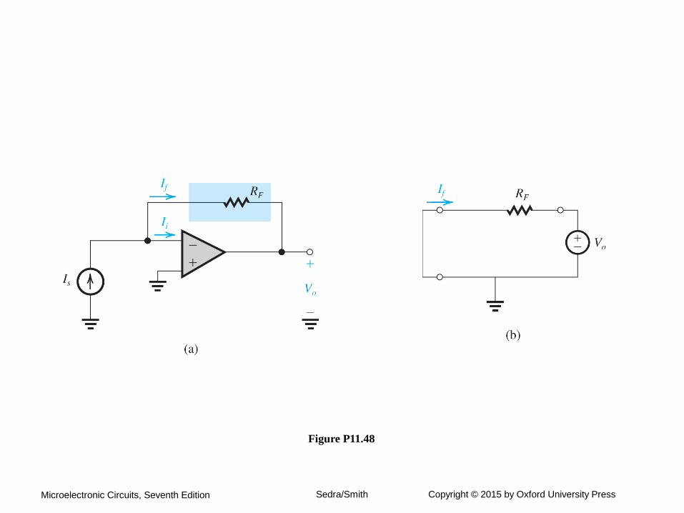
Figure P11.48
Microelectronic Circuits, Seventh Edition Sedra/Smith Copyright © 2015 by Oxford University Press
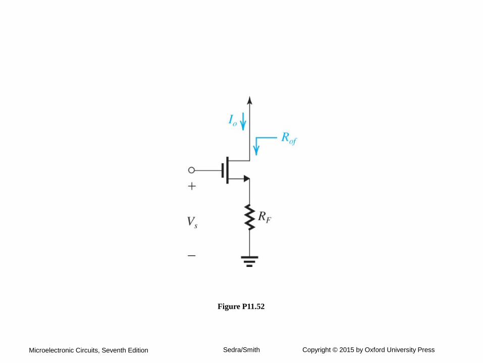
Figure P11.52
Microelectronic Circuits, Seventh Edition Sedra/Smith Copyright © 2015 by Oxford University Press
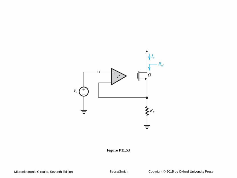
Figure P11.53
Microelectronic Circuits, Seventh Edition Sedra/Smith Copyright © 2015 by Oxford University Press
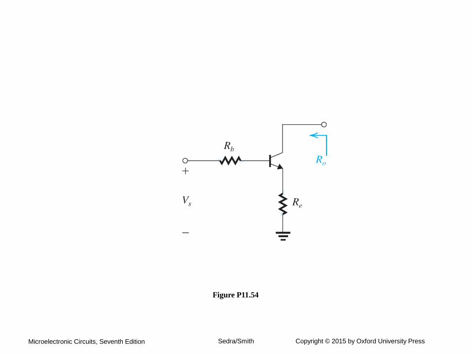
Figure P11.54
Microelectronic Circuits, Seventh Edition Sedra/Smith Copyright © 2015 by Oxford University Press
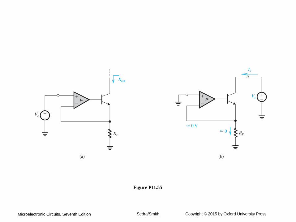
Figure P11.55
Microelectronic Circuits, Seventh Edition Sedra/Smith Copyright © 2015 by Oxford University Press
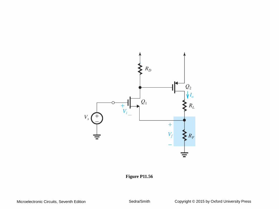
Figure P11.56
Microelectronic Circuits, Seventh Edition Sedra/Smith Copyright © 2015 by Oxford University Press
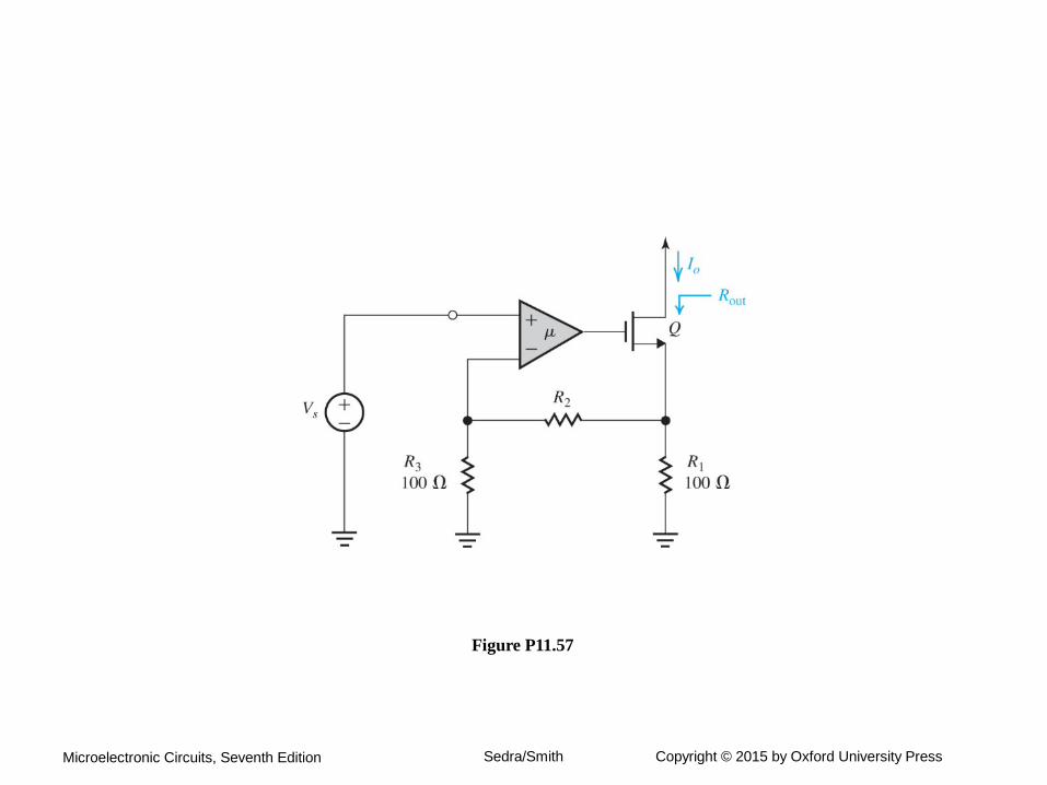
Figure P11.57
Microelectronic Circuits, Seventh Edition Sedra/Smith Copyright © 2015 by Oxford University Press
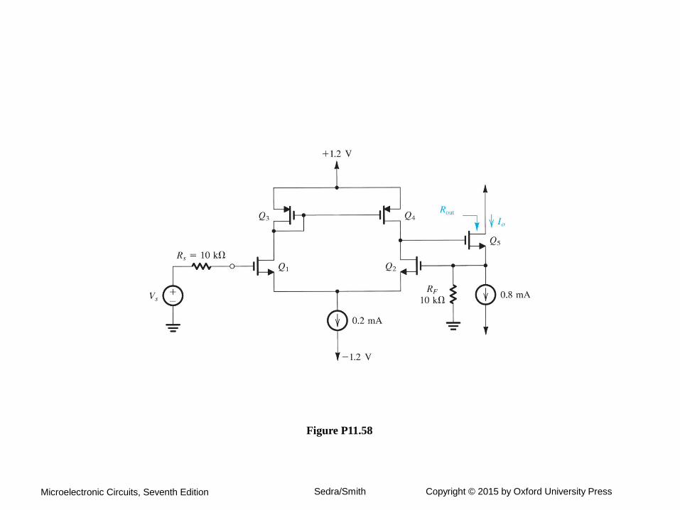
Figure P11.58
Microelectronic Circuits, Seventh Edition Sedra/Smith Copyright © 2015 by Oxford University Press
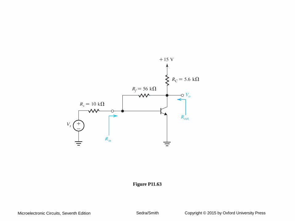
Figure P11.63
Microelectronic Circuits, Seventh Edition Sedra/Smith Copyright © 2015 by Oxford University Press
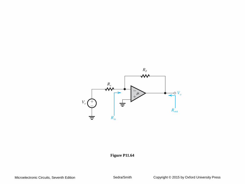
Figure P11.64
Microelectronic Circuits, Seventh Edition Sedra/Smith Copyright © 2015 by Oxford University Press
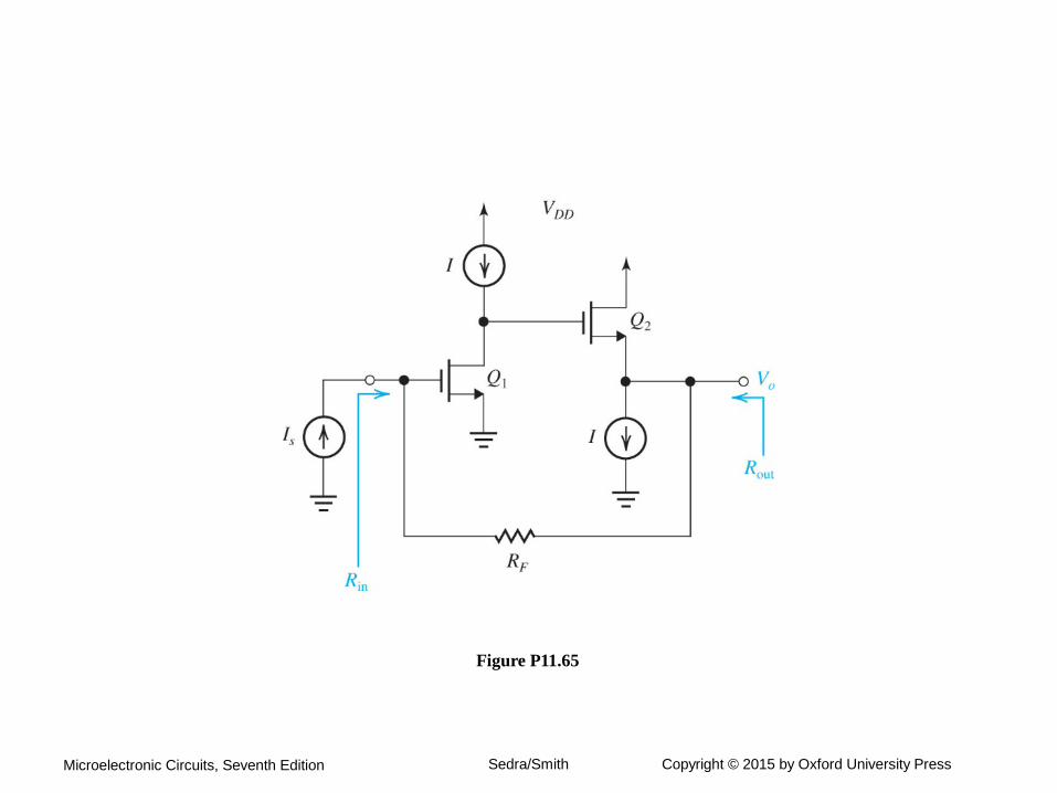
Figure P11.65
Microelectronic Circuits, Seventh Edition Sedra/Smith Copyright © 2015 by Oxford University Press
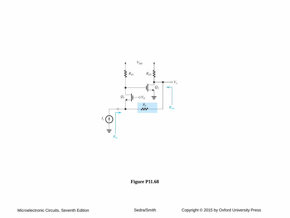
Figure P11.68
Microelectronic Circuits, Seventh Edition Sedra/Smith Copyright © 2015 by Oxford University Press
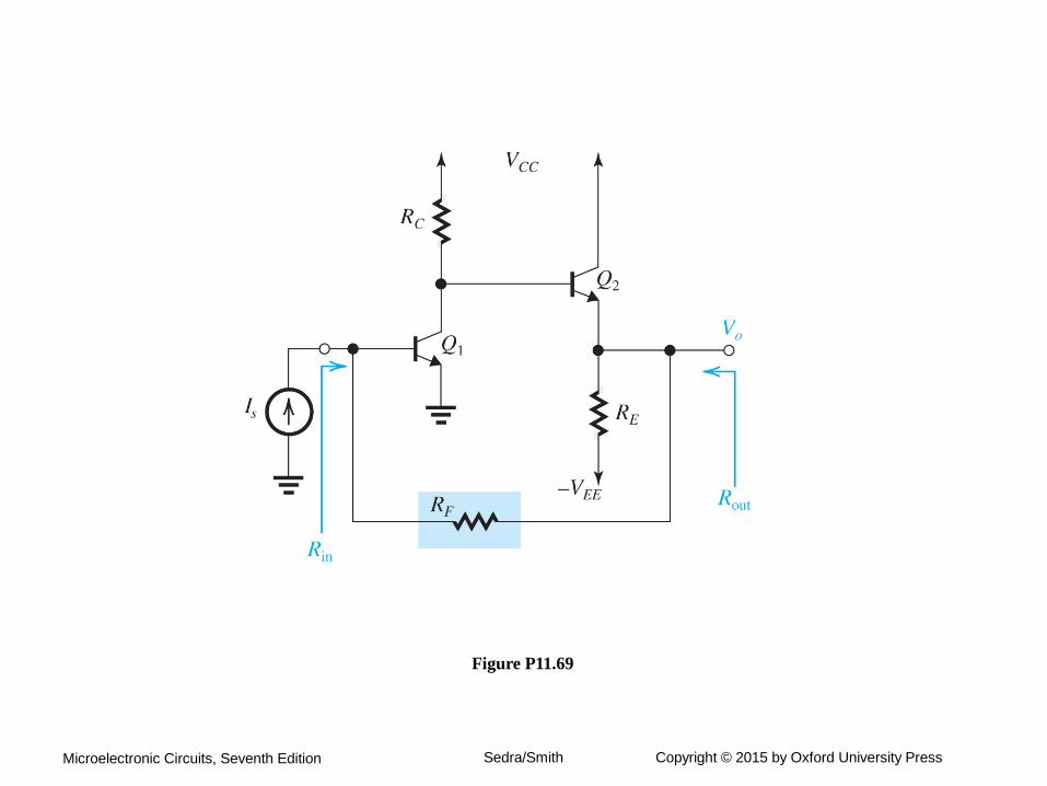
Figure P11.69
Microelectronic Circuits, Seventh Edition Sedra/Smith Copyright © 2015 by Oxford University Press
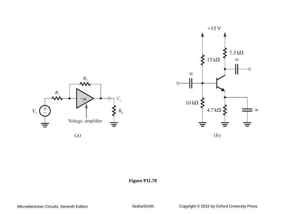
Figure P11.70
Microelectronic Circuits, Seventh Edition Sedra/Smith Copyright © 2015 by Oxford University Press
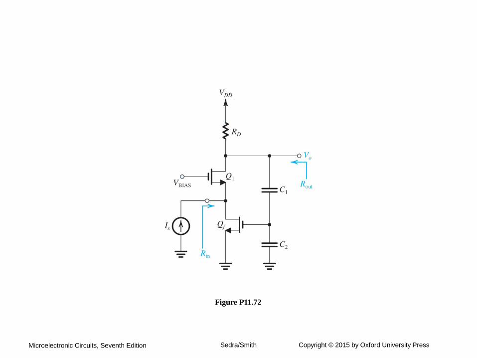
Figure P11.72
Microelectronic Circuits, Seventh Edition Sedra/Smith Copyright © 2015 by Oxford University Press
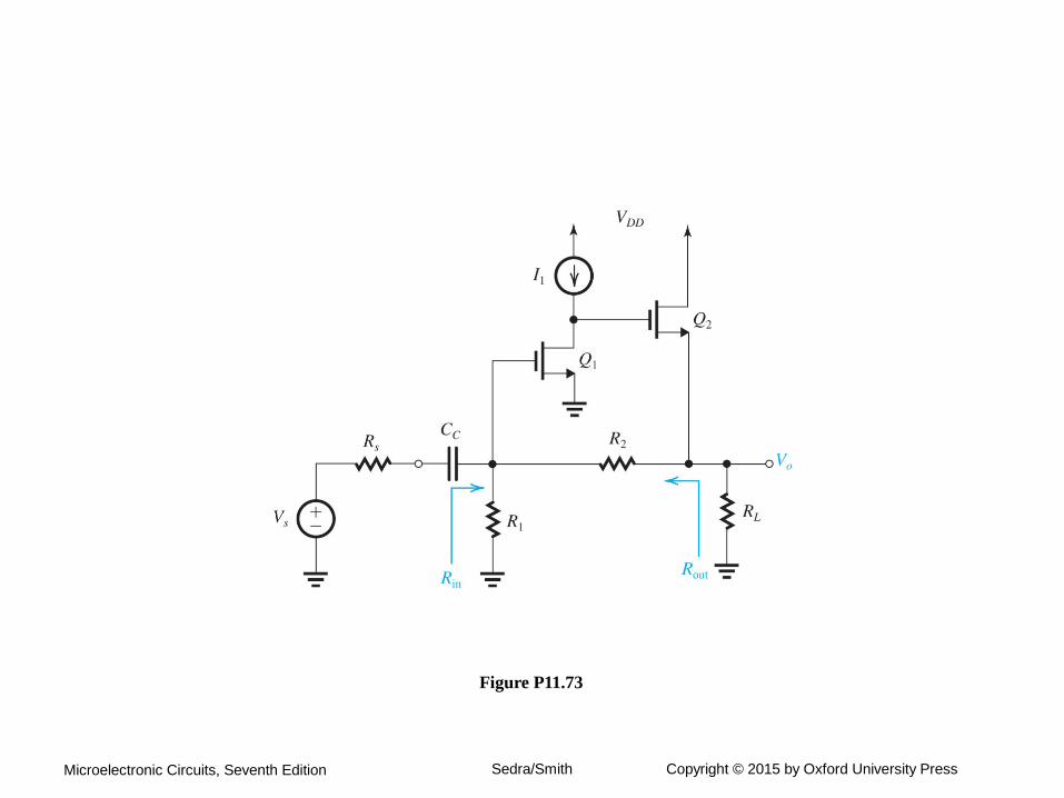
Figure P11.73
Microelectronic Circuits, Seventh Edition Sedra/Smith Copyright © 2015 by Oxford University Press
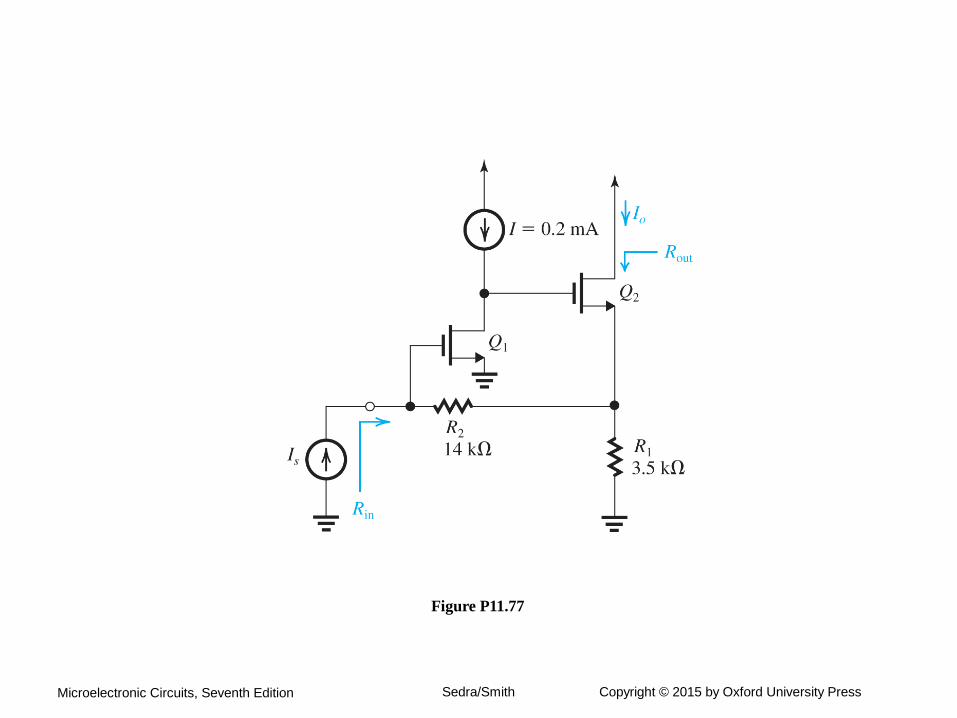
Figure P11.77
Microelectronic Circuits, Seventh Edition Sedra/Smith Copyright © 2015 by Oxford University Press
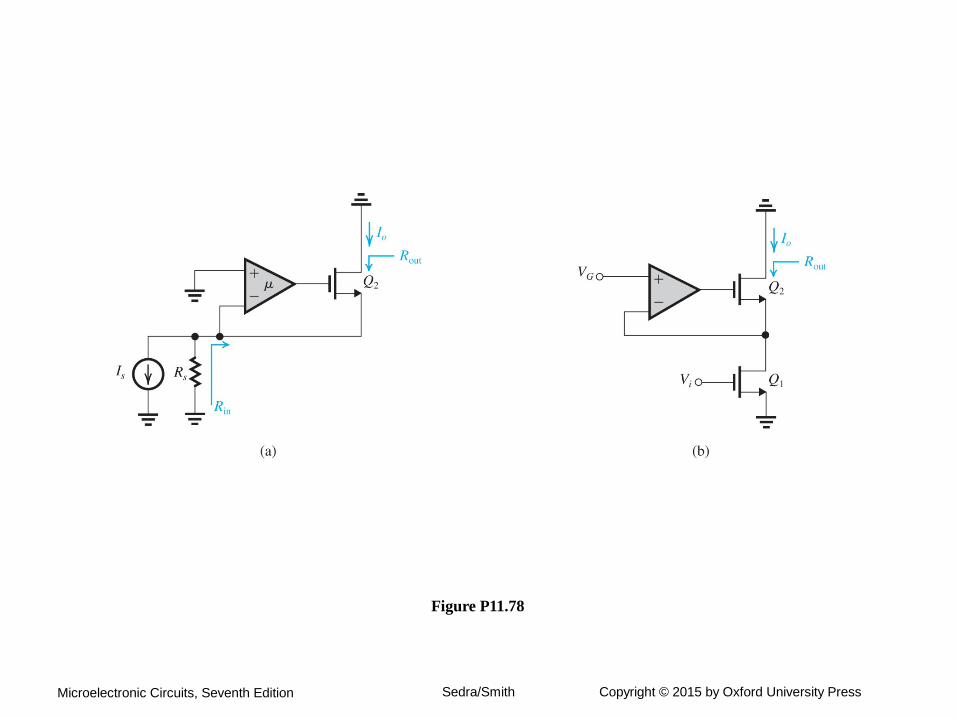
Figure P11.78
Microelectronic Circuits, Seventh Edition Sedra/Smith Copyright © 2015 by Oxford University Press
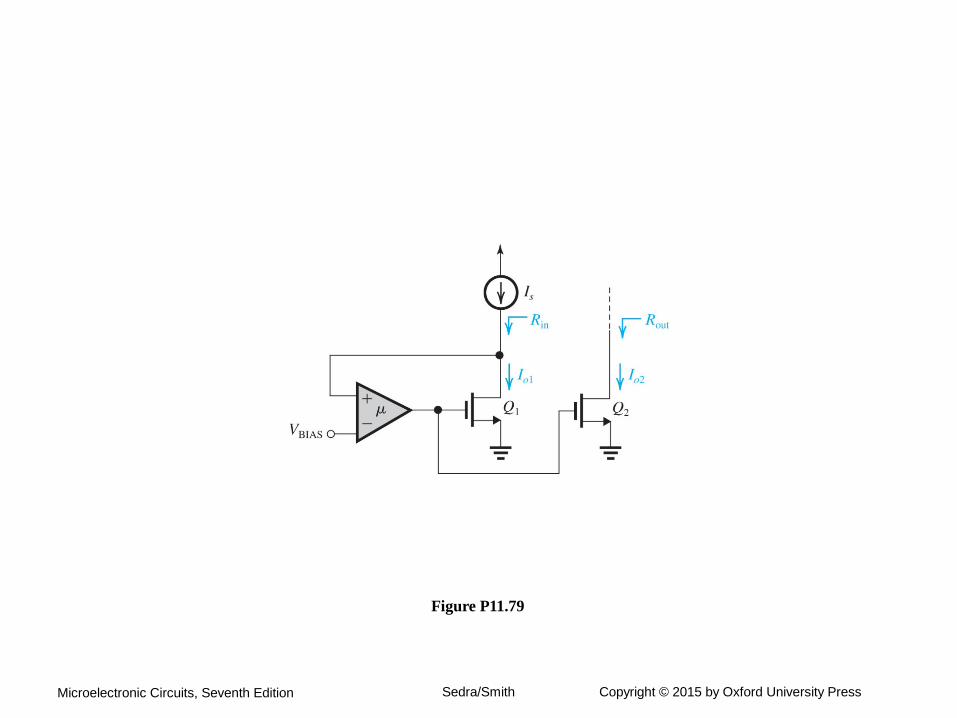
Figure P11.79
Microelectronic Circuits, Seventh Edition Sedra/Smith Copyright © 2015 by Oxford University Press
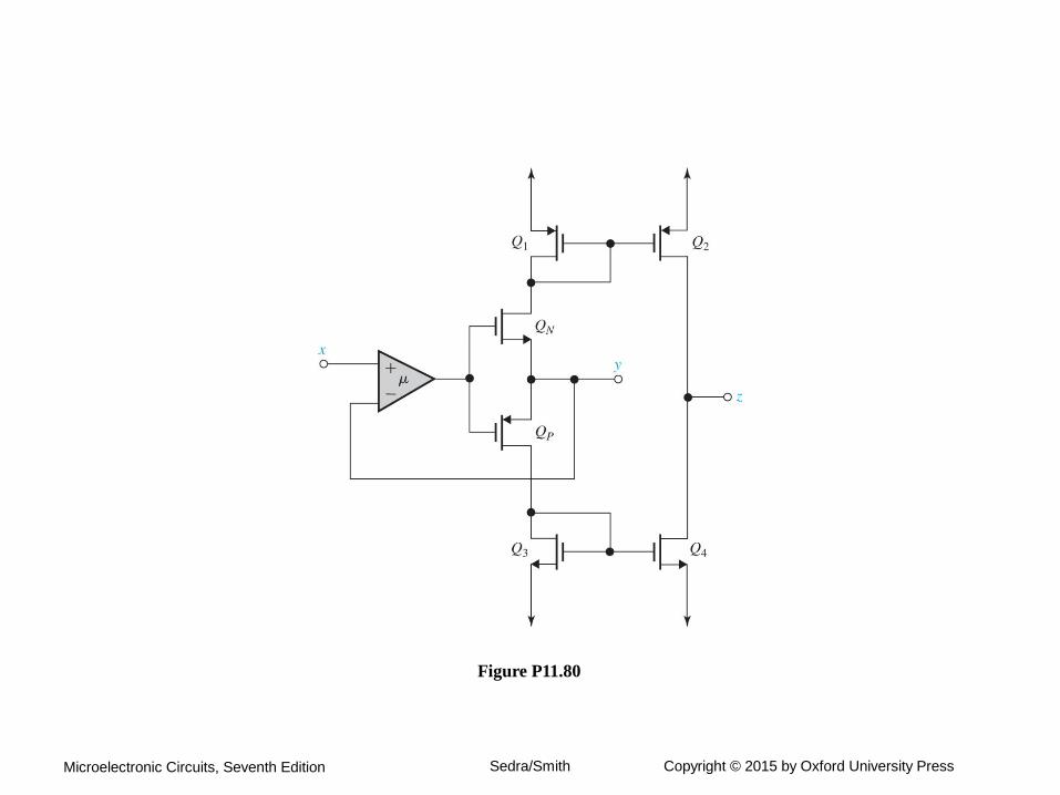
Figure P11.80
Microelectronic Circuits, Seventh Edition Sedra/Smith Copyright © 2015 by Oxford University Press
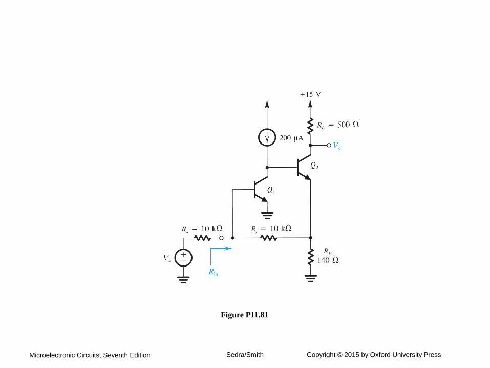
Figure P11.81

Microelectronic Circuits, Seventh Edition Sedra/Smith Copyright © 2015 by Oxford University Press
Figure P11.82
Microelectronic Circuits, Seventh Edition Sedra/Smith Copyright © 2015 by Oxford University Press
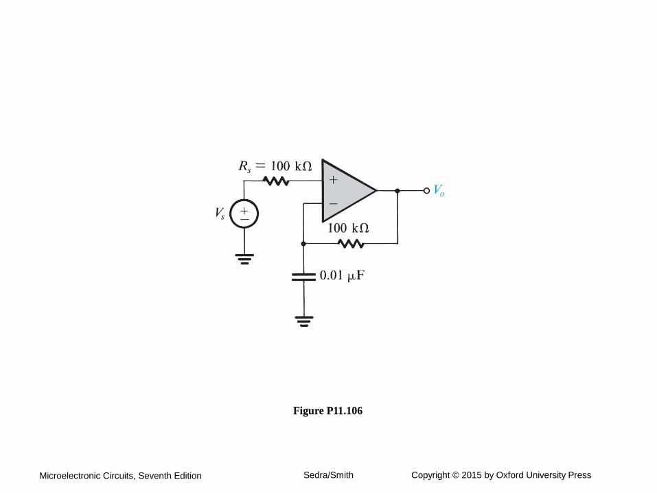
Figure P11.106