Embed Size (px)
Citation preview

IMAGE SENSOR SOLUTIONS
D E V I C E P E R F O R M A N C E S P E C I F I C A T I O N
KAF -0402E/ME 768 (H) x 512 (V) Enhanced Response Full-Frame CCD
January 29, 2003 Revision 1
K A F - 0 4 0 2 E / M E R e v . 1 w w w . k o d a k . c o m / g o / i m a g e r s 5 8 5 - 7 2 2 - 4 3 8 5 E m a i l : i m a g e r s @ k o d a k . c o m

IMAGE SENSOR SOLUTIONS
2
TIMING DIAGRAMS ..........................................13
TABLE OF CONTENTS
DEVICE DESCRIPTION ....................................4
ARCHITECTURE...............................................4 MICRO LENSES ................................................4
IMAGE ACQUISITION .......................................5
CHARGE TRANSPORT ....................................5
OUTPUT STRUCTURE.....................................5
DARK REFERENCE PIXELS ............................5
DUMMY PIXELS................................................5
PHYSICAL DESCRIPTION................................6 PIN DESCRIPTION ............................................6
PERFORMANCE ...............................................7 ELECTRO OPTICAL SPECIFICATIONS..................7 SPECTRAL RESPONSE......................................8 COSMETIC SPECIFICATION................................9
Cosmetic Definitions..................................9 OPERATION....................................................10
ABSOLUTE MAXIMUM RATINGS .......................10 DC OPERATING CONDITIONS..........................11 AC OPERATING CONDITION............................12 AC TIMING CONDITIONS.................................12
PHYSICAL DESCRIPTION..............................16 PACKAGE DRAWING .......................................16
QUALITY ASSURANCE AND RELIABILITY ...14
ORDERING INFORMATION ...........................15 AVAILABLE PART CONFIGURATIONS ................15
REVISION CHANGES....................................16
TABLE OF FIGURES
FIGURE 1 FUNCTIONAL BLOCK DIAGRAM ....... 4
FIGURE 3 OUTPUT SCHEMATIC ..................... 5
FIGURE 4 PACKAGE PIN DESIGNATION .......... 6
FIGURE 5 SPECTRAL RESPONSE................... 8
FIGURE 6 EXAMPLE OUTPUT STRUCTURE LOAD DIAGRAM.................................. 11
FIGURE 7 TIMING DIAGRAMS....................... 13
FIGURE 8 PACKAGE DIMENSIONS................ 16
K A F - 0 4 0 2 E / M E R e v . 1 w w w . k o d a k . c o m / g o / i m a g e r s 5 8 5 - 7 2 2 - 4 3 8 5 E m a i l : i m a g e r s @ k o d a k . c o m

IMAGE SENSOR SOLUTIONS
3
SUMMARY SPECIF ICATION
KODAK KAF-0402E/ME Image Sensor 768 (H) x 512 (V) Enhanced Response Full-Frame CCD
Description
The KAF-0402E/ME is a high performancemonochrome area CCD (charge-coupled device)image sensor with 768H x 512V photoactive pixels.It is designed for a wide range of image sensingapplications in the 350 nm to 1000 nm wavelengthband. Typical applications include military, scientific,and industrial imaging. Low dark current and goodcharge capacity result in 76 dB dynamic range atroom temperature. The sensor is built with a true two-phase CCDtechnology employing a transparent gate. Thistechnology simplifies the support circuits that drivethe sensor, reduces the dark current withoutcompromising charge capacity, and significantlyincreases to optical response compared totraditional front illuminated full frame sensors. The ME configuration adds micro lenses to thesurface of the CCD sensor. These lenses focus themajority of the light through the transparent gate,increasing the optical response further. The photoactive area is 6.91mm x 4.6 mm. Theimager is housed in a 24 -pin, 0.805” wide, dual inline package with 0.100” pin spacing.
K A F - 0 4 0 2 E / M E R e v . 1
w w w . k o d a k . c o m / g o / i m a g e r s 5 8 5 - 7 2 2 -Parameter Value
Architecture Full-Frame CCD; Enhanced Response
Total Number of Pixels 784 (H) x 520 (V)
Number of Active Pixels 768 (H) x 512 (V) = approx. 0.4M
Pixel Size 9.0µm (H) x 9.,0µm (V)
Imager Size 6.91(H)mm x 4.6(V)mm
Die Size 8.4mm (H) x 5.5mm (V)
Aspect Ratio 3:2
Saturation Signal 100,000 electrons
Quantum Efficiency
Peak with Microlens: 77%
Peak without Microlens: 65%
400 nm with Microlens: 45%
400nm without Microlens: 30%
Output Sensitivity 10 µV/e
Read Noise 15 electrons
Dark Current <10pA/cm2 @ 25°C
Dark Current Doubling Temperature 6.3°C
Dynamic Range 76 dB
Charge Transfer Efficiency >0.99999
Blooming Suppression None
Maximum Data Rate 10 MHz
4 3 8 5 E m a i l : i m a g e r s @ k o d a k . c o m

IMAGE SENSOR SOLUTIONS
4
KAF - 0402E/ME
DEVICE DESCRIPTION Architecture
Usable Active Image 768(H) x 512(V) 9 x 9 um pixels
3:2 aspect ratio
768 Active Pixels/Line
4 Dark 10 Inactive
Vrd
φ R Vdd Vout Vss
Sub Vog
φ H1 φ H2
φ V1
φ V2
Guard
2 Inactive 12 Dark
4 Dark lines
4 Dark lines
Figure 1 Functional block diagram The sensor consists of 784 parallel (vertical) CCD shift registers each 520 elements long. These registers act as both the photosensitive elements and as the transport circuits that allow the image to be sequentially read out of the sensor. The parallel (vertical) CCD registers transfer the image one line at a time into a single 796-element (horizontal) CCD shift register. The horizontal register transfers the charge to a single output amplifier. The output amplifier is a two-stage source follower that converts the photo-generated charge to a voltage for each pixel.
Micro lenses Micro lenses are formed along each row. They are effectively half of a cylinder centered on the transparent gates, extending continuously in the row direction. They act to direct the photons away from the polysilicon gate and through the transparent gate. This increases the response, especially at the shorter wavelengths (< 600 nm).
Micro lens
V1 electrode V2 electrode
K A F - 0 4 0 2 E / M E R e v . 1 w w w . k o d a k . c o m / g o / i m a g e r s 5 8 5 - 7 2 2 - 4 3 8 5 E m a i l : i m a g e r s @ k o d a k . c o m
Silicon

IMAGE SENSOR SOLUTIONS
5
Image Acquisition An electronic representation of an image is formed when incident photons falling on the sensor plane create electron-hole pairs within the sensor. These photon induced electrons are collected locally by the formation of potential wells at each photogate or pixel site. The number of electrons collected is linearly dependent on light level and exposure time and non-linearly dependent on wavelength. When the pixel's capacity is reached, excess electrons will leak into the adjacent pixels within the same column. This is termed blooming. During the integration period, the φV1 and φV2 register clocks are held at a constant (low) level. See Figure 7 Timing diagrams. Charge Transport Referring again to “Figure 7 Timing diagrams”, the integrated charge from each photogate is transported to the output using a two-step process. Each line (row) of charge is first transported from the vertical CCD to the horizontal CCD register using the φV1 and φV2 register clocks. The horizontal CCD is presented a new line on the falling edge of φV2 while φH1 is held high. The horizontal CCD then transports each line, pixel by pixel, to the output structure by alternately clocking the φH1 and φH2 pins in a complementary fashion. On each falling edge of φH2 a new charge packet is transferred onto a floating diffusion and sensed by the output amplifier. Output Structure Charge presented to the floating diffusion is converted into a voltage and current amplified in order to drive off-chip loads. The resulting voltage change seen at the output is linearly related to the amount of charge placed on the floating diffusion. Once the signal has been sampled by the system electronics, the reset gate (φR) is clocked to remove the signal and the floating diffusion is reset to the potential applied by Vrd. (see Figure 3 Output schematic ). More signal at the floating diffusion reduces the voltage seen at the output pin. In order to activate the output structure, an off-chip load must be added to the Vout pin of the device such as shown in Fig 4. Dark Reference Pixels There are 4 light shielded pixels at the beginning of each line, and 12 at the end. There are 4 dark lines at the start of every frame and 4 dark lines at
the end of each frame. Under normal circumstances, these pixels do not respond to light. However, dark reference pixels in close proximity to an active pixel can scavenge signal depending on light intensity and wavelength and therefore will not represent the true dark signal. Dummy Pixels Within the horizontal shift register are 10 leading additional pixels that are not associated with a column of pixels within the vertical register. These pixels contain only horizontal shift register dark current signal and do not respond to light. A few leading dummy pixels may scavenge false signal depending on operating conditions. There are two more dummy pixels at the end of each line.
FloatingDiffusion
HCCDChargeTransfer
SourceFollower#1
SourceFollower#2
Vrd
R
Vog
H2
H2
H1
VDD
Vout
H1
Figure 3 Output schematic
K A F - 0 4 0 2 E / M E R e v . 1 w w w . k o d a k . c o m / g o / i m a g e r s 5 8 5 - 7 2 2 - 4 3 8 5 E m a i l : i m a g e r s @ k o d a k . c o m
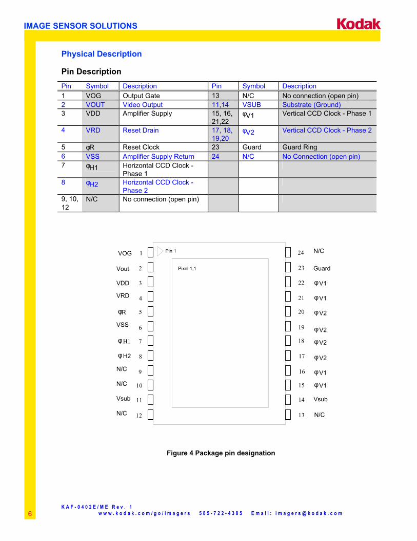
IMAGE SENSOR SOLUTIONS
Physical Description
Pin Description Pin Symbol Description Pin Symbol Description 1 VOG Output Gate 13 N/C No connection (open pin) 2 VOUT Video Output 11,14 VSUB Substrate (Ground) 3 VDD Amplifier Supply 15, 16,
21,22 φV1 Vertical CCD Clock - Phase 1
4 VRD Reset Drain 17, 18, 19,20
φV2 Vertical CCD Clock - Phase 2
5 φR Reset Clock 23 Guard Guard Ring 6 VSS Amplifier Supply Return 24 N/C No Connection (open pin) 7 φH1 Horizontal CCD Clock -
Phase 1
8 φH2 Horizontal CCD Clock - Phase 2
9, 10, 12
N/C No connection (open pin)
Pin 1
Pixel 1,1
24
23
22
21
20
19
18
17
16
15
14
13
Guard
φ V1
φ V1
Vsub
φ V2
φ V2
φ V2
φ V2
φ V1
1
2
3
4
5
6
7
8
9
10
11
12
VOG
Vout
VDD
VRD
φR
φ H2
φ H1
VSS
φ V1
N/C
N/C
N/C
N/C
Vsub
N/C
Figure 4 Package pin designation
K A F - 0 4 0 2 E / M E R e v . 1 w w w . k o d a k . c o m / g o / i m a g e r s 5 8 5 - 7 2 2 - 4 3 8 5 E m a i l : i m a g e r s @ k o d a k . c o m 6
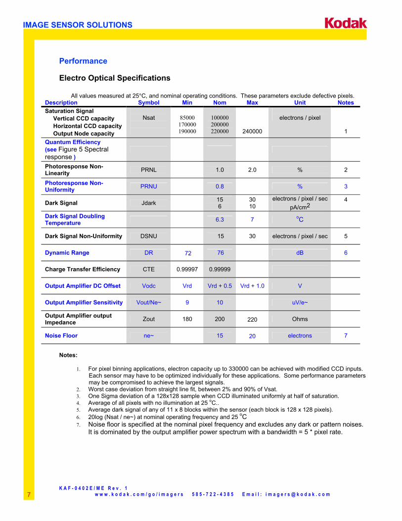
IMAGE SENSOR SOLUTIONS
Performance
Electro Optical Specifications
All values measured at 25°C, and nominal operating conditions. These parameters exclude defective pixels. Description Symbol Min Nom Max Unit Notes Saturation Signal Vertical CCD capacity Horizontal CCD capacity Output Node capacity
Nsat
85000
170000 190000
100000 200000 220000
240000
electrons / pixel
1
Quantum Efficiency (see Figure 5 Spectral response )
Photoresponse Non-Linearity PRNL 1.0 2.0 % 2
Photoresponse Non-Uniformity PRNU 0.8 % 3
Dark Signal Jdark 15 6
30 10
electrons / pixel / sec pA/cm2
4
Dark Signal Doubling Temperature 6.3 7 oC
Dark Signal Non-Uniformity DSNU 15 30 electrons / pixel / sec 5
Dynamic Range DR 72 76 dB 6
Charge Transfer Efficiency CTE 0.99997 0.99999
Output Amplifier DC Offset Vodc Vrd Vrd + 0.5 Vrd + 1.0 V
Output Amplifier Sensitivity Vout/Ne~ 9 10 uV/e~
Output Amplifier output Impedance Zout 180 200 220 Ohms
Noise Floor ne~ 15 20 electrons 7
Notes:
1. For pixel binning applications, electron capacity up to 330000 can be achieved with modified CCD inputs.
Each sensor may have to be optimized individually for these applications. Some performance parameters may be compromised to achieve the largest signals.
2. Worst case deviation from straight line fit, between 2% and 90% of Vsat. 3. One Sigma deviation of a 128x128 sample when CCD illuminated uniformly at half of saturation. 4. Average of all pixels with no illumination at 25 oC.. 5. Average dark signal of any of 11 x 8 blocks within the sensor (each block is 128 x 128 pixels). 6. 20log (Nsat / ne~) at nominal operating frequency and 25 oC 7. Noise floor is specified at the nominal pixel frequency and excludes any dark or pattern noises.
It is dominated by the output amplifier power spectrum with a bandwidth = 5 * pixel rate.
K A F - 0 4 0 2 E / M E R e v . 1 w w w . k o d a k . c o m / g o / i m a g e r s 5 8 5 - 7 2 2 - 4 3 8 5 E m a i l : i m a g e r s @ k o d a k . c o m 7

IMAGE SENSOR SOLUTIONS
Spectral Response
KAF-0402E/ME Spectral Response
0
0.1
0.2
0.3
0.4
0.5
0.6
0.7
0.8
0.9
1
400 500 600 700 800 900 1000
Wavelength (nm)
Abs
olut
e Q
uant
um E
ffici
ency
KAF-0402ME (Microlens) Standard KAF-0402E
Figure 5 Spectral response
K A F - 0 4 0 2 E / M E R e v . 1 w w w . k o d a k . c o m / g o / i m a g e r s 5 8 5 - 7 2 2 - 4 3 8 5 E m a i l : i m a g e r s @ k o d a k . c o m 8

IMAGE SENSOR SOLUTIONS
Cosmetic Specification Defect tests performed at T=25oC
Grade Point Defects Cluster Defects Column
C1 <5 0 0
C2 <10 <4 0
768,512
1,1 768,1
1,512
Cosmetic Definitions Point Defect DARK: A pixel which deviates by more than 6% from neighboring pixels
when illuminated to 70% of saturation, OR BRIGHT: A Pixel with dark current > 5000 e/pixel/sec at 25C. Cluster Defect A grouping of not more than 5 adjacent point defects. Column Defect 1) A grouping of >5 contiguous point defects along a single column.
2) A column containing a pixel with dark current > 12,000e/pixel/sec (bright column).
3) A column that does not meet the minimum vertical CCD charge capacity (low charge capacity column). 4) A column which loses more than 250 e under 2Ke illumination (trap defect).
Neighboring pixels The surrounding 128 x 128 pixels or ±64 columns/rows. Defect Separation Column and cluster defects are separated by no less than two
(2) pixels in any direction (excluding single pixel defects).
K A F - 0 4 0 2 E / M E R e v . 1 w w w . k o d a k . c o m / g o / i m a g e r s 5 8 5 - 7 2 2 - 4 3 8 5 E m a i l : i m a g e r s @ k o d a k . c o m 9

IMAGE SENSOR SOLUTIONS
Operation
Absolute Maximum Ratings
Description Symbol Min Max Unit Notes Diode Pin Voltages Vdiode 0 20 V 1,2 Gate Pin Voltages Vgate1 -16 16 V 1,3,6 Output Bias Current Iout -10 mA 4 Output Load Capacitance Cload 15 pF 4 Storage Temperature T 100 oC Humidity RH 5 90 % 5
Notes:
1. Referenced to pin Vsub or between each pin in this group. 2. Includes pins: Vrd, Vdd, Vss, Vout. 3. Includes pins: φV1, φV2, φH1, φH2, Vog, Vlg. φR. 4. Avoid shorting output pins to ground or any low impedance source during operation. 5. T=25°C. Excessive humidity will degrade MTTF. 6. This sensor contains gate protection circuits to provide some protection against ESD
events. The circuits will turn on when greater than 16 volts appears between any two gate pins. Permanent damage can result if excessive current is allowed to flow under these conditions.
CAUTION: This device contains limited protection against Electrostatic Discharge (ESD). Devices should be handled in accordance with strict ESD procedures for Class 0 devices (JESD22 Human Body Model) or Class A (Machine Model). Refer to Application Note MTD/PS-0224, “Electrostatic Discharge Control”
K A F - 0 4 0 2 E / M E R e v . 1 w w w . k o d a k . c o m / g o / i m a g e r s 5 8 5 - 7 2 2 - 4 3 8 5 E m a i l : i m a g e r s @ k o d a k . c o m 10
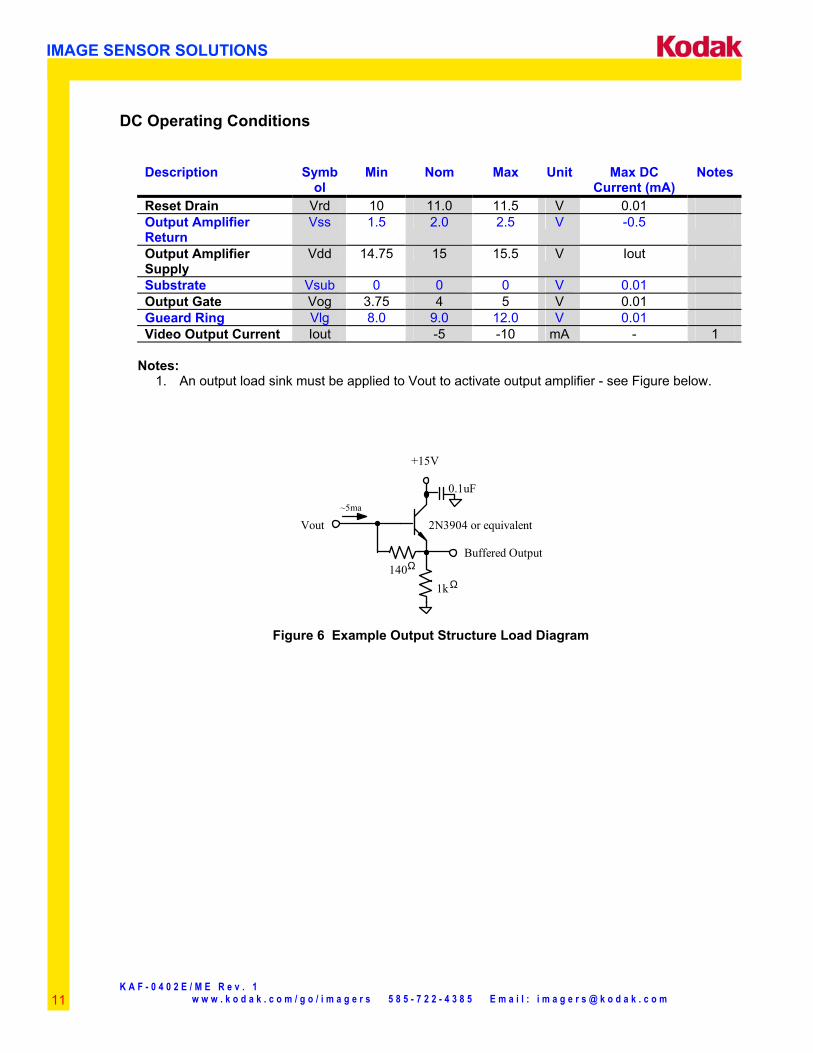
IMAGE SENSOR SOLUTIONS
DC Operating Conditions
Description Symbol
Min Nom Max Unit Max DC Current (mA)
Notes
Reset Drain Vrd 10 11.0 11.5 V 0.01 Output Amplifier Return
Vss 1.5 2.0 2.5 V -0.5
Output Amplifier Supply
Vdd 14.75 15 15.5 V Iout
Substrate Vsub 0 0 0 V 0.01 Output Gate Vog 3.75 4 5 V 0.01 Gueard Ring Vlg 8.0 9.0 12.0 V 0.01 Video Output Current Iout -5 -10 mA - 1
Notes:
1. An output load sink must be applied to Vout to activate output amplifier - see Figure below.
+15V
0.1uF
Vout
Buffered Output
1kΩ140Ω
2N3904 or equivalent~5ma
Figure 6 Example Output Structure Load Diagram
K A F - 0 4 0 2 E / M E R e v . 1 w w w . k o d a k . c o m / g o / i m a g e r s 5 8 5 - 7 2 2 - 4 3 8 5 E m a i l : i m a g e r s @ k o d a k . c o m 11

IMAGE SENSOR SOLUTIONS
AC Operating Condition Description Symbol Level Min Nom Max Unit Effective
Capacitance Vertical CCD Clock - Phase 1
φV1 Low High
-10.5 -0.5
-10.0 0
-9.5 1.0
V V
6 nF (all ØV1 pins)
Vertical CCD Clock - Phase 2
φV2 Low High
-10.5 -0.5
-10.0 0
-9.5 1.0
V V
6 nF (all ØV2 pins)
Horizontal CCD Clock - Phase 1
φH1 Low Amplitude
-4.5 9.5
-4.0 10.0
-3.5 10.5
V V
50pF
Horizontal CCD Clock - Phase 2
φH2 Low Amplitude
-4.5 9.5
-4.0 10.0
-3.5 10.5
V V
50pF
Reset Clock φR Low Amplitude
-3.0 5.0
-2.0 6.0
-1.75 7.0
V V
5pF
Notes:
1. All pins draw less than 10uA DC current. 2. Capacitance values relative to VSUB.
AC Timing Conditions
Description Symbol Min Nom Max Unit Notes φH1, φH2 Clock Frequency fH 4 10 MHz 1, 2, 3 Pixel Period (1 Count) te 100 250 ns φH1, φH2 Setup Time tφHS 0.5 1 us φV1, φV2 Clock Pulse Width tφV 1.5 2 us 2 Reset Clock Pulse Width tφR 10 20 ns 4 Readout Time treadout 43.7 107 ms 5 Integration Time tint 6 Line Time tline 84.1 206 us 7
Notes:
1. 50% duty cycle values. 2. CTE may degrade above the nominal frequency. 3. Rise and fall times (10/90% levels) should be limited to 5-10% of clock period. Cross-over of
register clocks should be between 40-60% of amplitude. 4. φR should be clocked continuously. 5. treadout = (520*tline) 6. Integration time is user specified. Longer integration times will degrade noise performance due
to dark signal fixed pattern and shot noise. 7. tline = (3*tφv) + tφHS + (796*te) +te
K A F - 0 4 0 2 E / M E R e v . 1 w w w . k o d a k . c o m / g o / i m a g e r s 5 8 5 - 7 2 2 - 4 3 8 5 E m a i l : i m a g e r s @ k o d a k . c o m 12

IMAGE SENSOR SOLUTIONS
Timing diagrams Frame Timing
tReadout
Line 1 2 519 520
1 Frame = 520 Lines
φV1
φV2
φH1
φH2
tint
Pixel Timing
φR
φH1
φH2
Vout
tφR
Vsat Vdark
Vsub
Vodc
1 count te
Line Timing
1 line = 796 Pixels
φV1
φV2
φH1
φH2
φR
796 counts
tφHS te
tφV
tφV
Vpix
Line Content
Photoactive
Dark Reference
Dummy Pixels
1-10 11-14 15 - 782 783-794 795-796
Vsat Saturated pixel video output Vdark Video output signal in no light situation, not zero due to Vpix Pixel video output signal level, more electrons =more Vodc Video level offset with respect to Vsub Analog
* See Image Aquisition section
Figure 7 Timing diagrams
K A F - 0 4 0 2 E / M E R e v . 1 w w w . k o d a k . c o m / g o / i m a g e r s 5 8 5 - 7 2 2 - 4 3 8 5 E m a i l : i m a g e r s @ k o d a k . c o m 13

IMAGE SENSOR SOLUTIONS
QUALITY ASSURANCE AND RELIABILITY Quality Strategy: All image sensors will conform to the specifications stated in this document. This will be accomplished through a combination of statistical process control and inspection at key points of the production process. Typical specification limits are not guaranteed but provided as a design target. For further information refer to ISS Application Note MTD/PS-0292, Quality and Reliability. Replacement: All devices are warranted against failure in accordance with the terms of Terms of Sale. This does not include failure due to mechanical and electrical causes defined as the liability of the customer below. Liability of the Supplier: A reject is defined as an image sensor that does not meet all of the specifications in this document upon receipt by the customer. Liability of the Customer: Damage from mechanical (scratches or breakage), electrostatic discharge (ESD), or other electrical misuse of the device beyond the stated absolute maximum ratings, which occurred after receipt of the sensor by the customer, shall be the responsibility of the customer. Cleanliness: Devices are shipped free of mobile contamination inside the package cavity. Immovable particles and scratches that are within the imager pixel area and the corresponding cover glass region directly above the pixel sites are also not allowed. The cover glass is highly susceptible to particles and other contamination. Touching the cover glass must be avoided. See ISS Application Note MTD/PS-0237, Cover Glass Cleaning for Image Sensors, for further information. ESD Precautions: Devices are shipped in static-safe containers and should only be handled at static-safe workstations. See ISS Application Note MTD/PS-0224, Electrostatic Discharge Control, for handling recommendations. Reliability: Information concerning the quality assurance and reliability testing procedures and results are available from the Image Sensor Solutions and can be supplied upon request. For further information refer to ISS Application Note MTD/PS-0292, Quality and Reliability. Test Data Retention: Image sensors shall have an identifying number traceable to a test data file. Test data shall be kept for a period of 2 years after date of delivery. Mechanical: The device assembly drawing is provided as a reference. The device will conform to the published package tolerances.
K A F - 0 4 0 2 E / M E R e v . 1 w w w . k o d a k . c o m / g o / i m a g e r s 5 8 5 - 7 2 2 - 4 3 8 5 E m a i l : i m a g e r s @ k o d a k . c o m 14

IMAGE SENSOR SOLUTIONS
ORDERING INFORMATION
Available Part Configurations
Type Description Glass Configuration
KAF-0402E Monochrome
KAF-0402ME Monochrome, microlens Please contact Image Sensor Solutions for available part numbers. Address all inquiries and purchase orders to:
Image Sensor Solutions Eastman Kodak Company Rochester, New York 14650-2010 Phone: (585) 722-4385 Fax: (585) 477-4947 E-mail: [email protected]
Kodak reserves the right to change any information contained herein without notice. All information furnished by Kodak is believed to be accurate. WARNING: LIFE SUPPORT APPLICATIONS POLICY Kodak image sensors are not authorized for and should not be used within Life Support Systems without the specific written consent of the Eastman Kodak Company. Product warranty is limited to replacement of defective components and does not cover injury or property or other consequential damages.
K A F - 0 4 0 2 E / M E R e v . 1 w w w . k o d a k . c o m / g o / i m a g e r s 5 8 5 - 7 2 2 - 4 3 8 5 E m a i l : i m a g e r s @ k o d a k . c o m 15

IMAGE SENSOR SOLUTIONS
Physical Description
Package Drawing
Figure 8 Package dimensions
K A F - 0 4 0 2 E / M E R e v . 1 w w w . k o d a k . c o m / g o / i m a g e r s 5 8 5 - 7 2 2 - 4 3 8 5 E m a i l : i m a g e r s @ k o d a k . c o m 16

IMAGE SENSOR SOLUTIONS
REVISION CHANGES
Revision Number
Release Date Description of Changes
A 11/11/02 Initial release; modifications to existing KAF-0402 spec with new format from KAF-1402E spec
B 1/6/03 New spectral response data.
1 1/27/03 First formal release.
K A F - 0 4 0 2 E / M E R e v . 1 w w w . k o d a k . c o m / g o / i m a g e r s 5 8 5 - 7 2 2 - 4 3 8 5 E m a i l : i m a g e r s @ k o d a k . c o m 17