Embed Size (px)
Citation preview

TC603X2/3/6/8AC TO DC
- 1 -
TC6032/3/4/5/6
FEATURES ◆ Built-in High Voltage Power BJT
◆ Proprietary NC-Cap/super-QR/PSR-IITM (Quasi-Resonant & Primary Side Regulation) Control:
● ±4% CC and CV Precision
● Proprietary “Audio Noise Cancellation” Control
● Built-in “Fast Dynamic Response” Control to Meet USB Charge Requirements
● Proprietary “Zero-Output Startup” Control ● Proprietary “Smart Output Short Protection” ● without External Compensation/Filtering
Capacitor Needed ● Max. 50V Output for AC/DC LED Lighting
◆ Direct Drive of Low Cost BJT
◆ Proprietary Cable Drop Compensation
◆ Multi Mode Control
◆ Frequency Jitter for Better EMI
◆ Dynamic Base Drive for High Efficiency
◆ Wide VDD Operating Range
◆ 10.8V UVLO Hysteresis Window
◆ Cycle-by-Cycle Current Limiting
◆ Leading Edge Blanking (LEB)
◆ Built-in Soft Start, Pin Floating Protection
◆ VDD UVLO, OVP, VOUT OVP, OLP, SCP
APPLICATIONS ◆ Battery chargers
◆ Replaces linear transformer and RCC SMPS
◆ Small power adapter
◆ AC/DC LED lighting
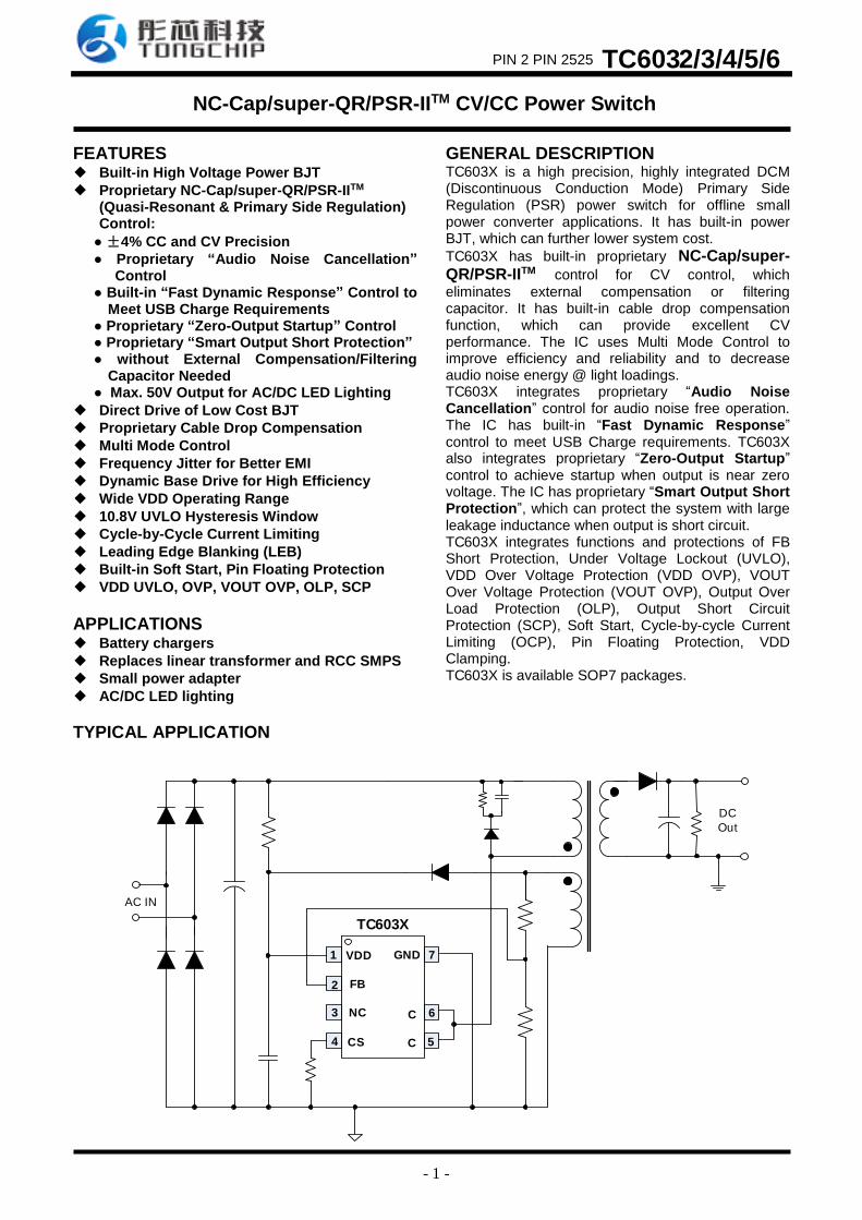
GENERAL DESCRIPTION TC603X is a high precision, highly integrated DCM (Discontinuous Conduction Mode) Primary Side Regulation (PSR) power switch for offline small power converter applications. It has built-in power BJT, which can further lower system cost.
TC603X has built-in proprietary NC-Cap/super-QR/PSR-IITM control for CV control, which
eliminates external compensation or filtering capacitor. It has built-in cable drop compensation function, which can provide excellent CV performance. The IC uses Multi Mode Control to improve efficiency and reliability and to decrease audio noise energy @ light loadings. TC603X integrates proprietary “Audio Noise Cancellation” control for audio noise free operation. The IC has built-in “Fast Dynamic Response” control to meet USB Charge requirements. TC603X also integrates proprietary “Zero-Output Startup” control to achieve startup when output is near zero voltage. The IC has proprietary “Smart Output Short Protection”, which can protect the system with large leakage inductance when output is short circuit. TC603X integrates functions and protections of FB Short Protection, Under Voltage Lockout (UVLO), VDD Over Voltage Protection (VDD OVP), VOUT Over Voltage Protection (VOUT OVP), Output Over Load Protection (OLP), Output Short Circuit Protection (SCP), Soft Start, Cycle-by-cycle Current Limiting (OCP), Pin Floating Protection, VDD Clamping. TC603X is available SOP7 packages.
TYPICAL APPLICATION
AC IN
DC
Out
7
6
5
1
NC
FB
CS
GNDVDD
2
3
4
C
C
TC603X
NC-Cap/super-QR/PSR-IITM CV/CC Power Switch
PIN 2 PIN 2525
- 2 -
TC6032/3/4/5/6
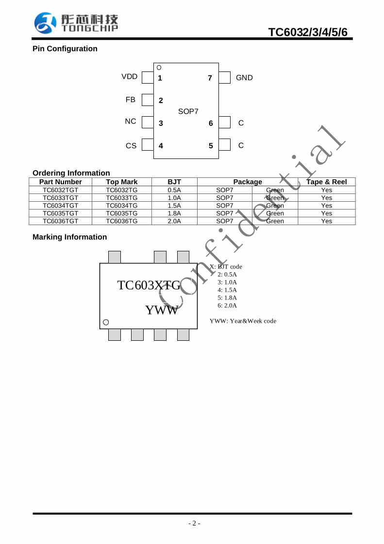
Pin Configuration
FB
1
2
3
VDD GND
C
SOP7
4
7
6
5CS C
NC
Ordering Information
Part Number Top Mark BJT Package Tape & Reel TC6032TGT TC6032TG 0.5A SOP7 Green Yes
TC6033TGT TC6033TG 1.0A SOP7 Green Yes
TC6034TGT TC6034TG 1.5A SOP7 Green Yes
TC6035TGT TC6035TG 1.8A SOP7 Green Yes
TC6036TGT TC6036TG 2.0A SOP7 Green Yes
Marking Information
TC 603XTG
YWW
X: BJT code
2: 0.5A
3: 1.0A
4: 1.5A
5: 1.8A
6: 2.0A
YWW: Year&Week code
- 3 -
TC6032/3/4/5/6
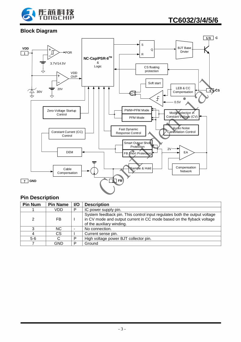
Block Diagram
5/6 C
CS4
Soft start
CS floating
protection
R
S
Q
2V
POR
VDD
1
3.7V/14.5V
20V
VDD
OVP
30V
DEM
Sample & Hold
Constant Current (CC)
Control
Compensation
Network
EA
0.5V
GND7
NC-Cap/PSR-IITM
&
Logic
FB2
Cable
Compensation
Mode Selection in
Constant Voltage (CV)
PWM+PFM Mode
PFM Mode
Zero-Voltage Startup
Control
BJT Base
Drvier
Smart Output Short
Protection
FB Short Protection
LEB & CC
Compensation
Audio Noise
Cancellation ControlFast Dynamic
Response Control
Pin Description
Pin Num Pin Name I/O Description 1 VDD P IC power supply pin.
2 FB I System feedback pin. This control input regulates both the output voltage in CV mode and output current in CC mode based on the flyback voltage of the auxiliary winding.
3 NC - No connection.
4 CS I Current sense pin.
5-6 C P High voltage power BJT collector pin.
7 GND P Ground

- 4 -
TC6032/3/4/5/6
Recommended Operation Conditions (Note 1) Parameter Value Unit
Supply Voltage, VDD 7 to 16 V
Operating Ambient Temperature -40 to 85 oC
Maximum Switching Frequency 70K Hz
Absolute Maximum Ratings (Note 2)
Parameter Value Unit VDD DC Supply Voltage 22 V
VDD DC Clamp Current 10 mA
CS voltage range -0.3 to 7 V
FB voltage range -0.7 to 7 V
Collector to Emitter Voltage 850 V
Package Thermal Resistance (SOP-7) θJA 120 oC/W
θJC 60 oC/W
Maximum Junction Temperature 150 oC
Operating Temperature Range -40 to 85 oC
Storage Temperature Range -65 to 150 oC
Lead Temperature (Soldering, 10sec.) 260 oC
ESD Capability, HBM (Human Body Model) 3 kV
ESD Capability, MM (Machine Model) 250 V
ELECTRICAL CHARACTERISTICS
(TA = 25OC, VDD=14V, if not otherwise noted)
Symbol Parameter Test Conditions Min Typ Max Unit
Supply Voltage (VDD) Section
I_Startup VDD Start up Current VDD =UVLO(OFF)-1V 1 3 uA
I_VDD_Op Operation Current VDD=14V 0.8 1.5 mA
UVLO(OFF) VDD Under Voltage Lockout Exit (Startup)
13.5 14.5 15.5 V
UVLO(ON) VDD Under Voltage Lockout Enter 3.4 3.7 4 V
VDD_OVP VDD Over Voltage Protection trigger
18 20 22 V
T_Softstart Soft Start Time 2 mSec
Feedback Input Section(FB Pin)
VFB_EA_Ref Internal Error Amplifier(EA) reference input
1.98 2.0 2.02 V
VFB_DEM Demagnetization comparator threshold
25 mV
Tmin_OFF Minimum OFF time 2 uSec
Tmax_OFF Maximum OFF time 3.3 mSec
VFB_Short Output Short Circuit Threshold 1.2 V
TFB_Short Output Short Circuit Debounce Time
65 mSec
VFB_OVP Output Over Voltage Protection Threshold
2.8 V
TCC/TDEM Ratio between switching period in CC mode and demagnetization time
2
ICable_max Max Cable compensation current 60 uA
Current Sense Input Section (CS Pin)
T_blanking CS Leading Edge Blanking Time 500 nSec
Vth_OC_max Max. Current limiting threshold 490 500 510 mV
TD_OC Over Current Detection and Control Delay
100 nSec

- 5 -
TC6032/3/4/5/6
Power BJT Section
BVCEO
6032
Collector-emitter breakdown voltage
IC=1mA 450
V
6033 IC=10mA 480
6034 IC=10mA 450
6035 IC=10mA 450
6036 IC=10mA 450
BVCBO
6032
Collector-base breakdown voltage
IC=1mA 750
V
6033 IC=1mA 850
6034 IC=1mA 800
6035 IC=1mA 800
6036 IC=1mA 800
BVEBO
6032
Emitter-base breakdown voltage
IE=1mA 11
V
6033 IE=1mA 11
6034 IE=1mA 9
6035 IE=1mA 9
6036 IE=1mA 9
VCE(sat)
6032
Collector-emitter saturation voltage
IC=0.1A, IB=20mA 0.6
V
6033 IC=0.1A, IB=20mA 0.5
IC=0.5A, IB=0.1A 0.8
6034 IC=0.5A, IB=0.1A 0.25
IC=1.5A, IB=0.5A 0.75
6035 IC=1A, IB=0.2A 0.4
6036 IC=1.0A, IB=0.2A 0.4
IC=2.0A, IB=0.5A 0.6
Hfe
6032
DC current gain
VCE=20V, IC=20mA 20 30
6033 VCE=5V, IC=0.1A 20 30
6034 VCE=5V, IC=0.2A 15 25
6035 VCE=6.5V, IC=0.2A 20 30
6036 VCE=5V, IC=1A 15 25
Note 1. Stresses beyond those listed under “Absolute Maximum Ratings” may cause permanent damage to the device. These are stress ratings only, and functional operation of the device at these or any other conditions beyond those indicated in the operational sections of the specifications is not implied. Exposure to absolute maximum rating conditions for extended periods may affect device reliability.
Note 2. The device is not guaranteed to function outside its operating conditions.

- 6 -
TC6032/3/4/5/6
OPERATION DESCRIPTION TC603X is a high performance, highly integrated DCM (Discontinuous Conduction Mode) Primary Side Regulation (PSR) power switch. The built-in high precision CV/CC control makes it very suitable for offline small power converter applications.
◆ PSR Technology Introduction Assuming the system works in DCM mode, the power transfer function is given by
ooSpkm IVfILP 2
2
(Eq.1)
In the equation above, P is output power, Vo and Io are system output voltage and current respectively,
η is system power transfer efficiency, Lm is
transformer primary inductance, fs is system switching frequency, Ipk is primary peak current in a switching cycle. The following figure illustrates the waveform in a switching cycle.
Base Drive for
power BJT
Primary Inductor
Current
Demagnetization
Time (Tdem)
Ipk
Ipk_s
Secondary Inductor
Current
Auxiliary Winding
Voltage
DEM Signal
Plateau sampling
for CV control
Fig.1
In the figure shown above, the IC generates a demagnetization signal (DEM) in each switching cycle through auxiliary winding. Tdem is demagnetization time for CV/CC control. In DCM mode, Tdem can be expressed as;
pk
P
Sdem
m
o IN
NT
L
V (Eq.2)
In Eq.2, Np and Ns are primary and secondary winding turns respectively. Combined with Eq.1 and Eq. 2, the average output current can be expressed as:
demS
S
Ppko Tf
N
NII
2
(Eq.3)
CC (Constant Current) Control Scheme From Eq.3, it can be easily seen that there are two ways to implement CC control: one is PFM (Pulse Frequency Modulation), the control scheme is to keep Ipk to be constant, let the product of Ts and Tdem (fs*Tdem) to be a constant. In this way, Io will be a value independent to the variation of Vo,
Lm, and line input voltage. Another realization method is PWM duty control, the control scheme is to keep fs to be constant, let the product of Tdem and Ipk (Tdem*Ipk) to be a constant, in another words, by modulating system duty cycle to realize a constant Io independent to the variation of Vo, Lm and line voltages. TC603X adopts PFM for CC control, the product of Ts and Tdem is given by
5.0 demS Tf (Eq.4)
CV (Constant Voltage) Control Scheme
CV control should sample the plateau of auxiliary winding voltage in flyback phase, as shown in Fig.1 The CV control has many implementations, for example, PWM, or PFM, or a combination of both one. In TC603X, the CV control adopts proprietary multi mode control, as mention below. The output voltage can be sensed via the auxiliary winding. During MOSFET turn-off time, the energy stored in the primary winding is transferred to the secondary side. The auxiliary voltage reflects the output voltage as shown in Fig.1 and it is given by
)( VVN
NV O
S
AUXAUX (Eq.5)
Where ΔV indicates the voltage drop of the output
diode. As shown in Fig.2, via a resistor divider connected between the auxiliary winding and FB (pin 1), the auxiliary voltage is sampled at the middle of the de-magnetization and it is hold until the next sampling. The sampled voltage is compared with reference voltage (typical 2.0V) and the difference is amplified. The error amplifier output reflects the load condition and controls the switching off time to regulate the output voltage, thus constant output voltage can be achieved.
7
6
5
1
VDD
NC
CS
GNDFB
2
3
4
C
C
TC603XR1
R2
NAUX
Fig.2
◆ Startup Current / Startup Control / Operating Current
Startup current of TC603X is designed to be very low (typically 1uA) so that VDD could be charged up above UVLO(OFF) threshold level and device starts up quickly. The operating current in TC603X is as small as 0.8mA (typical). The small operating current results in higher efficiency and reduces the VDD hold-up capacitance requirement.

- 7 -
TC6032/3/4/5/6
◆ NC-Cap/PSR-IITM Introduction
● ±4% Precision CV/CC Performance
TC603X can achieve less than±4% variation of
CC/CV precision due to the built-in CV accuracy improvement and CC line and load compensation, as shown in Fig.3.
● Proprietary “Audio Noise Cancellation” Control TC603X has a proprietary “Audio Noise Cancellation” control, which can achieve audio noise free operation in the whole loading range.
● Built-in Fast Dynamic Response Control to Meet USB Charge Requirements In TC603X, a fast dynamic response control is integrated to improve system dynamic response performance, thus the charger system can meet the USB charge requirements.
● Smart Output Short Protection The output short circuit protection of conventional PSR system is based on the coupling between auxiliary winding and secondary winding. When output is short, the auxiliary winding cannot provide enough energy to the IC any more. In this way, the system will enter into auto-recovery mode protection. However, the IC may be wrongly supplied if the leakage inductance of the primary winding is large enough. In TC603X, if output short circuit occurs, the IC will detect the situation and enter into auto-recovery mode protection.
● Proprietary Zero-Output Startup Control Conventional PSR system may suffer startup failure when output voltage is near zero voltage, which means that there is a gap between OCP (CC point in PSR CV/CC system) and full loading. Larger OCP gap causes larger system cost. In TC603X, a proprietary “Zero-Output Startup Control” is adopted to achieve successful startup @ Vout≈0V, as shown in Fig.3.
Output Vo
Output Io
±4%
±4%
PWM+PFM ModePFM Mode
Conventional PSR will
start up fail @ Vout≈0V
“Zero-Voltage Startup Control” can start up @ Vout≈0V
Fig.3
● No External Compensation/Filtering Capacitor Needed TC603X uses a proprietary control to eliminate external compensation capacitor, which can simplify system design and lower system cost.
● Maximum 50V Output for LED Lighting TC603X can support maximum 50V output, which can be used in AC/DC LED lighting.
◆ Proprietary Cable Drop Compensation TC603X has a proprietary built-in cable voltage drop compensation block which can provide a constant output voltage at the end of the cable over the entire load range in CV mode.
◆ Multi Mode PSR Control for High Reliability , High Efficiency
Conventional pure PFM controlled PSR system may suffer transformer saturation issue when heavy loading. In TC603X, a proprietary multi mode control is adopted to suppress this issue, as shown in Fig.3. Around the full load, the system operates in PWM+PFM mode, which improve the system reliability. Under normal to light load conditions, the IC operates in PFM mode to achieve excellent regulation and high efficiency.
◆ Soft Start TC603X features an internal 2ms (typical) soft start that slowly increases the threshold of cycle-by-cycle current limiting comparator during startup sequence. Every startup process is followed by a soft start activation.
◆ Leading Edge Blanking (LEB) Each time the power BJT is switched on, a turn-on spike occurs across the sensing resistor. To avoid premature termination of the switching pulse, an internal leading edge blanking circuit is built in. During this blanking period (500ns, typical), the cycle-by-cycle current limiting comparator is disabled and cannot switch off the base driver.
◆ Minimum and Maximum OFF Time In TC603X, a minimum OFF time (typically 2us) is implemented to suppress ringing when BASE drive is pull off. The maximum OFF time in TC603X is typically 3.3ms, which provides a large range for frequency reduction. In this way, low standby power can be achieved.
◆ Pin Floating Protection In TC603X, if pin floating situation occurs, the IC is designed to have no damage to system.
◆ Built-in Load and AC Line CC Compensation
In conventional PSR system, the output CC (Constant Current) point can vary with output and AC line voltage. In TC603X the IC has built-in

- 8 -
TC6032/3/4/5/6
blocks to compensate the variation, as shown in Fig4. The IC can adjust CC point based on sensed output voltage and PFM duty. In this way, CC accuracy can be improved.
LEB
Sample & Hold
0.5V
AC Line
Compensation
Load
Compensation
CC Compensation
CS
FB
to
PFM
PFM Duty
TC603X
Fig.4
◆ Auto Recovery Mode Protection As shown in Fig.5, once a fault condition is detected, switching will stop. This will cause VDD to fall because no power is delivered form the auxiliary winding. When VDD falls to UVLO(on) (typical 3.7V), the protection is reset and the operating current reduces to the startup current, which causes VDD to rise. However, if the fault still exists, the system will experience the above mentioned process. If the fault has gone, the system resumes normal operation. In this manner, the auto restart can alternatively enable and disable the switching until the fault condition is disappeared.
Base switching
VDD
3.7V
14.5V
Protection Tiggers Fault Removed
Fig.5
◆ VDD Over Voltage Protection VDD OVP is implemented in TC603X and it is a protection of auto-recovery mode. If VDD is higher than 20V (TYP), VDD OVP protection will be trigged and the switch is turned off until VDD is lower than UVLO(on) (typical 3.7V).
◆ VOUT Over Voltage Protection If FB voltage during the sampling time is higher than OVP voltage (typical 2.8V), the counter will start to work. VOUT OVP protection will be trigged when the counter is counted to 3 continuously, and the switch is turned off until VDD is lower than UVLO(on) (typical 3.7V).

- 9 -
TC603XA/B/C
PACKAGE MECHANICAL DATA
- 10 -
TC603XA/B/C
Resale of TC ’s products or services with statements different from or beyond the parameters stated by SiFirst for that product or service voids all express and any implied warranties for the associated SiFirst’s product or service and is an unfair and deceptive business practice. TC. is not responsible or liable for any such statements.
TC ’s products are neither designed nor intended for use in military applications. SiFirst will not be held liable for any damages or claims resulting from the use of its products in military applications.
TC ’s products are not designed to be used as components in devices intended to support or sustain human
life. TC. will not be held liable for any damages or claims resulting from the use of its products in medical applications.