Embed Size (px)
Citation preview

Motion Controller for Stepper Motors Integrated Circuits
SHORT SPEC
TMC4361A DATASHEET TMC4361A Document Revision 1.10 • 2016-JUL-20 SHORT SPEC The S-ramp and sixPoint™ ramp motion controller for stepper motors is optimized for high velocities, allowing on-the-fly changes. TMC4361A offers SPI and Step/Dir interfaces, as well as an encoder interface for closed-loop operation.
NOTE:
TMC4361A is a product upgrade of TMC4361.
Features SPI Interfaces for µC with easy-to-use protocol.
SPI Interfaces for SPI motor stepper drivers.
Encoder interface for incremental or serial
encoders.
Closed-loop operation for Step and SPI drivers.
Integrated ChopSync™ and dcStep™ support.
Internal ramp generator generating S-shaped
ramps or sixPoint™ ramps supporting on-the-fly
changes.
Controlled PWM output.
Reference switch handling.
Hardware and virtual stop switches.
Extensive Support of TMC stepper motor drivers.
Applications
Textile, sewing machines
CCTV, security
Printers, scanners
ATM, cash recycler
Office automation
POS
Factory automation
Lab automation
Pumps and valves
Heliostat controllers
CNC machines
Robotics
Block Diagram: TMC4361A Interfaces & Features
Figure 2: Block Diagram
© 2015 TRINAMIC Motion Control GmbH & Co. KG, Hamburg,
Germany — Terms of delivery and rights to technical change
reserved. Download newest version at: www.trinamic.com.
Read entire documentation; especially the
Supplemental Directives in chapter 20 (page 228).
TMC4361
SPI to
Master
Safe Ramp Down
ISO 13485
Status Flags
Interrupt
Controller
Ref. Switch
Processing
Driver
Interface:
SPI /
Step/Dir
Ref. Switches
S-Ramp
Generatorincl. trapezoid,
rectangle, 4bows
SPI
Step/Dir
SPI to µC
INTR / TR to µC
Timer Unit
Power-on
Reset
Step
Sequencer
Current
Regulation
Encoder
Interface
Closed Loop
ABN
SSI
SPI
NFreeze
CLK
NRST
dcStep
START
Figure 1: Sample Image
TMC4361A Closed-Loop Drive
*Marking details are explained on page 227.

TMC4361A Datasheet | Document Revision 1.10 • 2016-JUL-20 2/234
© 2015 TRINAMIC Motion Control GmbH & Co. KG, Hamburg, Germany — Terms of delivery and
rights to technical change reserved. Download newest version at: www.trinamic.com .
Read entire documentation; especially the Supplemental Directives on page 228.
SHORT SPEC
Functional Scope of TMC4361A TMC4361A is a miniaturized high-performance motion controller for stepper motor drivers, particularly designed for fast and jerk-limited motion profile applications with a wide range of ramp profiles. The S-shaped or sixPoint™ velocity profile, closed-loop and open-loop features offer many configuration options to suit the user’s specifications, as presented below:
S-shaped ramp profiles are jerk-free. Seven ramp segments form the S-shaped
ramp that can be optimally adapted to suit the user’s requirements. High
torque with high velocities can be reached by calibrating the bows of the ramp,
as explained in this user manual.
Figure 3: S-shaped Velocity Profile
i More information on ramp configurations and other velocity profiles, e.g.
sixPoint™ ramps, are provided in chapter 6 (Page 28).
A typical hardware setup for closed-loop operation with a TMC262 stepper
motor gate driver is shown in the diagram below. In case internal MOSFETs are
desired, combine the TMC4361A with the TMC2620, the TMC261 or the
TMC2660.
Figure 4: Hardware Set-up for Closed-loop Operation with TMC262
A typical hardware setup for dcStep operation with a TMC2130 stepper motor
driver is shown in the diagram below. This feature is also available for TMC26x
stepper motor drivers.
Figure 5: Hardware Set-up for Open-loop Operation with TMC2130
Order Codes
Order code Description Size TMC4361A-LA Motion controller with closed-loop and dcStep features, QFN40 6 x 6 mm2
Table 1: TMC4361A Order Codes
v(t)
t
VMAX
µCTMC262
Motor Gate
Driver
MOSFE
TDriver
Stage
High level
interface M
TMC4361Motion
Controller
EncoderABN / SSI / SPI
SPI SPI
µC TMC2130Motor Driver
High level interface M
TMC4361Motion
Controller
SPI
SPI
dcStep™ signals
S/D
S-ShapedVelocity Profile
Closed-loop Operation Feature
Open-loop Operation with dcStep™ Feature
TMC4361A Datasheet | Document Revision 1.10 • 2016-JUL-20 3/234
© 2015 TRINAMIC Motion Control GmbH & Co. KG, Hamburg, Germany — Terms of delivery and
rights to technical change reserved. Download newest version at: www.trinamic.com .
Read entire documentation; especially the “Supplemental Directives” on page 228.
MAIN MANUAL
TABLE OF CONTENTS
TMC4361A DATASHEET .................................................................................................................. 1
SHORT SPEC .................................................................................................................................... 1
Features .......................................................................................................................................... 1
Applications ................................................................................................................................... 1
Block Diagram: TMC4361A Interfaces & Features ..................................................................... 1
Functional Scope of TMC4361A .................................................................................................... 2
Order Codes ................................................................................................................................... 2
TABLE OF CONTENTS ..................................................................................................................... 3
MAIN MANUAL ............................................................................................................................. 10
1. Pinning and Design-In Process Information ..................................................................... 10
Pin Assignment: Top View .............................................................................................................. 10
Pin Description ................................................................................................................................ 11
System Overview ............................................................................................................................. 13
2. Application Circuits .............................................................................................................. 14
TMC4361A Standard Connection: VCC=3.3V ............................................................................... 14
TMC4361A with TMC26x Stepper Connection ............................................................................ 14
TMC4361A with TMC248 Stepper Driver ..................................................................................... 15
TMC4361A with TMC2130 Stepper Driver ................................................................................... 15
3. SPI Interfacing ....................................................................................................................... 16
SPI Datagram Structure .................................................................................................................. 16
SPI Timing Description ................................................................................................................... 19
4. Input Filtering ....................................................................................................................... 20
Input Filtering Examples................................................................................................................. 22
Configuration of Step/Dir Input Filter........................................................................................... 23
5. Status Flags and Events ....................................................................................................... 24
Status Event Description ................................................................................................................ 25
SPI Status Bit Transfer .................................................................................................................... 26
Generation of Interrupts ................................................................................................................ 26
Connection of Multiple INTR Pins ................................................................................................. 27
6. Ramp Configurations for different Motion Profiles ......................................................... 28
Step/Dir Output Configuration ...................................................................................................... 29
Step/Dir Output Configuration Steps ........................................................................................... 29
STPOUT: Changing Polarity ........................................................................................................... 29
Altering the Internal Motion Direction ......................................................................................... 30
Configuration Details for Operation Modes and Motion Profiles ............................................ 31
Starting Point: Choose Operation Mode ...................................................................................... 32

TMC4361A Datasheet | Document Revision 1.10 • 2016-JUL-20 4/234
© 2015 TRINAMIC Motion Control GmbH & Co. KG, Hamburg, Germany — Terms of delivery and
rights to technical change reserved. Download newest version at: www.trinamic.com .
Read entire documentation; especially the “Supplemental Directives” on page 228.
MAIN MANUAL
Stop during Motion ......................................................................................................................... 32
Motion Profile Configuration ......................................................................................................... 33
No Ramp Motion Profile ................................................................................................................. 34
Trapezoidal 4-Point Ramp without Break Point .......................................................................... 35
Trapezoidal Ramp with Break Point ............................................................................................ 35
Position Mode combined with Trapezoidal Ramps .................................................................... 36
Configuration of S-Shaped Ramps ................................................................................................ 37
Changing Ramp Parameters during S-shaped Motion or Switching from Velocity to
Positiong Mode ................................................................................................................................................ 38
Configuration of S-shaped Ramp with ASTART and DFINAL........................................................ 38
S-shaped Mode and Positioning: Fast Motion ............................................................................ 39
Start Velocity VSTART and Stop Velocity VSTOP ............................................................................ 40
S-shaped Ramps with Start and Stop Velocity ............................................................................ 44
Combined Use of VSTART and ASTART for S-shaped Ramps ....................................................... 45
sixPoint Ramps ................................................................................................................................ 46
U-Turn Behavior .............................................................................................................................. 47
Continuous Velocity Motion Profile for S-shaped Ramps ......................................................... 48
Internal Ramp Generator Units ..................................................................................................... 49
Clock Frequency .............................................................................................................................. 49
Velocity Value Units ........................................................................................................................ 49
Acceleration Value Units ................................................................................................................ 49
Bow Value Units .............................................................................................................................. 50
Overview of Minimum and Maximum Values: ............................................................................ 50
7. External Step Control and Electronic Gearing .................................................................. 51
Description of Electronic Gearing ................................................................................................. 52
Indirect External Control ................................................................................................................ 52
Switching from External to Internal Control ................................................................................ 53
8. Reference Switches .............................................................................................................. 55
Hardware Switch Support .............................................................................................................. 56
Stop Slope Configuration for Hard or Linear Stop Slopes ......................................................... 56
How Active Stops are indicated and reset to Free Motion ........................................................ 57
How to latch Internal Position on Switch Events ........................................................................ 57
Virtual Stop Switches ...................................................................................................................... 58
Enabling Virtual Stop Switches ...................................................................................................... 58
Virtual Stop Slope Configuration ................................................................................................... 58
How Active Virtual Stops are indicated and reset to Free Motion ............................................ 59
Home Reference Configuration .................................................................................................... 60
Home Event Selection..................................................................................................................... 61
HOME_REF Monitoring ................................................................................................................... 61
Homing with STOPL or STOPR ....................................................................................................... 62
Target Reached / Position Comparison ....................................................................................... 63
Connecting several Target-reached Pins ..................................................................................... 63
Use of TARGET_REACHED Output ................................................................................................. 64

TMC4361A Datasheet | Document Revision 1.10 • 2016-JUL-20 5/234
© 2015 TRINAMIC Motion Control GmbH & Co. KG, Hamburg, Germany — Terms of delivery and
rights to technical change reserved. Download newest version at: www.trinamic.com .
Read entire documentation; especially the “Supplemental Directives” on page 228.
MAIN MANUAL
Position Comparison of Internal Values ...................................................................................... 65
Repetitive and Circular Motion ...................................................................................................... 66
Repetitive Motion to XTARGET ...................................................................................................... 66
Activating Circular Motion .............................................................................................................. 66
Uneven or Noninteger Microsteps per Revolution .................................................................... 67
Release of the Revolution Counter ............................................................................................... 68
Blocking Zones ................................................................................................................................ 68
Activating Blocking Zones during Circular Motion...................................................................... 68
Circular Motion with and without Blocking Zone ....................................................................... 69
9. Ramp Timing and Synchronization .................................................................................... 70
Basic Synchronization Settings...................................................................................................... 71
Start Signal Trigger Selection ......................................................................................................... 71
User-specified Impact Configuration of Timing Procedure ....................................................... 71
Delay Definition between Trigger and internally generated Start Signal ................................ 72
Active START Pin Output Configuration ....................................................................................... 72
Ramp Timing Examples .................................................................................................................. 73
Shadow Register Settings ............................................................................................................... 76
Shadow Register Configuration Options ..................................................................................... 77
Delayed Shadow Transfer .............................................................................................................. 81
Pipelining Internal Parameters ..................................................................................................... 83
Configuration and Activation of Target Pipeline ......................................................................... 83
Using the Pipeline for different internal Registers ..................................................................... 84
Pipeline Mapping Overview ........................................................................................................... 85
Cyclic Pipelining ............................................................................................................................... 86
Pipeline Examples ........................................................................................................................... 86
Masterless Synchronization of Several Motion Controllers via START Pin .............................. 89
10. Serial Data Output ............................................................................................................... 90
Getting Started with TMC Motor Drivers ..................................................................................... 91
Sine Wave Lookup Tables .............................................................................................................. 92
Actual Current Values Output ....................................................................................................... 93
How to Program the Internal MSLUT ........................................................................................... 94
Setup of MSLUT Segments ............................................................................................................. 95
Current Waves Start Values ........................................................................................................... 96
Default MSLUT ................................................................................................................................. 96
Explanatory Notes for Base Wave Inclinations ........................................................................... 97
SPI Output Interface Configuration Parameters ......................................................................... 99
How to enable SPI Output Communication ................................................................................ 99
Setup of SPI Output Timing Configuration ................................................................................ 100
Current Diagrams .......................................................................................................................... 101
Change of Microstep Resolution ................................................................................................. 101
Cover Datagrams Communication between µC and Driver .................................................... 101
Sending Cover Datagrams ........................................................................................................... 102
Configuring Automatic Generation of Cover Datagrams ........................................................ 103

TMC4361A Datasheet | Document Revision 1.10 • 2016-JUL-20 6/234
© 2015 TRINAMIC Motion Control GmbH & Co. KG, Hamburg, Germany — Terms of delivery and
rights to technical change reserved. Download newest version at: www.trinamic.com .
Read entire documentation; especially the “Supplemental Directives” on page 228.
MAIN MANUAL
Overview: TMC Motor Driver Connections ................................................................................ 104
TMC Stepper Motor Driver Settings ............................................................................................ 104
TMC Motor Driver Response Datagram and Status Bits.......................................................... 105
Events and Interrupts based on Motor Driver Status Bits....................................................... 105
Stall Detection and Stop-on-Stall ................................................................................................ 106
TMC23x, TMC24x Stepper Motor Driver .................................................................................... 107
TMC23x Setup ................................................................................................................................ 107
TMC24x Setup ................................................................................................................................ 107
TMC23x/24x Status Bits ................................................................................................................ 108
Automatic Fullstep Switchover for TMC23x/24x ....................................................................... 108
Mixed Decay Configuration for TMC23x/24x ............................................................................ 109
ChopSync Configuration for TMC23x/24x Stepper Drivers ..................................................... 109
Doubling ChopSync Frequency during Standstill ..................................................................... 109
Using TMC24x stallGuard Characteristics .................................................................................. 110
TMC26x Stepper Motor Driver .................................................................................................... 112
TMC26x Setup (SPI mode) ........................................................................................................... 112
TMC26x Setup (S/D mode) ........................................................................................................... 112
Sending Cover Datagrams to TMC26x ....................................................................................... 113
Automatic Continuous Streaming of Cover Datagrams for TMC26x ..................................... 113
TMC26x SPI Mode: Automatic Fullstep Switchover ................................................................. 114
TMC26x S/D Mode: Automatic Fullstep Switchover ................................................................. 114
TMC 26x S/D Mode: Change of Current Scaling Parameter .................................................... 115
TMC26x Status Bits ....................................................................................................................... 116
TMC26x Status Response ............................................................................................................. 116
TMC389 Stepper Motor Driver .................................................................................................... 116
TMC2130 Stepper Motor Driver .................................................................................................. 117
Set-up TMC2130 Support (SPI Mode) ......................................................................................... 117
Set-up TMC2130 Support (S/D Mode) ........................................................................................ 117
Sending Cover Datagrams to TMC2130 ..................................................................................... 118
Automatic Continuous Streaming of Cover Datagrams for TMC2130 ................................... 118
TMC2130 SPI Mode: Automatic Fullstep Switchover ................................................................ 119
TMC2130 S/D Mode: Automatic Fullstep Switchover ............................................................... 119
TMC 2130 S/D Mode: Changing current Scaling Parameter .................................................... 119
TMC2130 Status Response .......................................................................................................... 120
Connecting Non-TMC Stepper Motor Driver or SPI-DAC at SPI output interface ................. 121
Connecting a SPI-DAC ................................................................................................................... 122
DAC Data Transfer ........................................................................................................................ 122
Changing SPI Output Protocol for SPI-DAC ............................................................................... 122
DAC Address Values ...................................................................................................................... 123
DAC Data Values ............................................................................................................................ 123
11. Current Scaling ................................................................................................................... 125
Hold Current Scaling ..................................................................................................................... 126
Freewheeling ................................................................................................................................. 126

TMC4361A Datasheet | Document Revision 1.10 • 2016-JUL-20 7/234
© 2015 TRINAMIC Motion Control GmbH & Co. KG, Hamburg, Germany — Terms of delivery and
rights to technical change reserved. Download newest version at: www.trinamic.com .
Read entire documentation; especially the “Supplemental Directives” on page 228.
MAIN MANUAL
Current Scaling during Motion .................................................................................................... 127
Drive Scaling .................................................................................................................................. 127
Alternative Drive Scaling .............................................................................................................. 127
Boost Current ................................................................................................................................ 128
Scale Mode Transition Process Control ..................................................................................... 129
Current Scaling Examples ............................................................................................................ 131
12. NFREEZE and Emergency Stop ........................................................................................... 133
Configuration of FREEZE Function .............................................................................................. 133
Configuration of DFREEZE for automatic Ramp Stop ................................................................ 134
13. Controlled PWM Output .................................................................................................... 135
PWM Output Generation and Scaling Possibilities ................................................................... 136
PWM Scale Example ...................................................................................................................... 137
PWM Output Generation for TMC23x/24x ................................................................................ 138
Switching between SPI and Voltage PWM Modes..................................................................... 139
14. dcStep Support for TMC26x or TMC2130 .......................................................................... 140
Enabling dcStep for TMC26x Stepper Motor Drivers ............................................................... 142
Setup: Minimum dcStep Velocity ................................................................................................ 143
Enabling dcStep for TMC2130 Stepper Motor Drivers ............................................................. 145
15. Decoder Unit: Connecting ABN, SSI, or SPI Encoders correctly .................................... 146
Selecting the correct Encoder...................................................................................................... 147
Disabling digital differential Encoder Signals ............................................................................ 148
Inverting of Encoder Direction .................................................................................................... 148
Encoder Misalignment Compensation ....................................................................................... 149
Incremental ABN Encoder Settings ............................................................................................. 150
Automatic Constant Configuration of Incremental ABN Encoder .......................................... 150
Manual Constant Configuration of Incremental ABN Encoder ............................................... 150
Incremental Encoders: Index Signal: N resp. Z ......................................................................... 151
Setup of Active Polarity for Index Channel ............................................................................... 151
Configuration of N Event .............................................................................................................. 151
External Position Counter ENC_POS Clearing ............................................................................ 152
Latching External Position ........................................................................................................... 153
Latching Internal Position ............................................................................................................ 153
Absolute Encoder Settings ........................................................................................................... 154
Singleturn or Multiturn Data ....................................................................................................... 154
Automatic Constant Configuration of Absolute Encoder ........................................................ 155
Manual Constant Configuration of incremental ABN Encoder ............................................... 155
Absolute Encoder Data Setup ..................................................................................................... 156
Emitting Encoder Data Variation ................................................................................................. 157
SSI Clock Generation..................................................................................................................... 158
Enabling Multicycle SSI request.................................................................................................. 159
Gray-encoded SSI Data Streams ................................................................................................ 159
SPI Encoder Data Evaluation ....................................................................................................... 160
TMC4361A Datasheet | Document Revision 1.10 • 2016-JUL-20 8/234
© 2015 TRINAMIC Motion Control GmbH & Co. KG, Hamburg, Germany — Terms of delivery and
rights to technical change reserved. Download newest version at: www.trinamic.com .
Read entire documentation; especially the “Supplemental Directives” on page 228.
MAIN MANUAL
SPI Encoder Mode Selection ........................................................................................................ 161
SPI Encoder Configuration via TMC4361A ................................................................................. 162
16. Possible Regulation Options with Encoder Feedback .................................................... 163
Feedback Monitoring .................................................................................................................... 163
Target-Reached during Regulation ............................................................................................. 163
PID-based Control of XACTUAL ..................................................................................................... 164
PID Readout Parameters .............................................................................................................. 164
PID Control Parameters and Clipping Values ............................................................................ 165
Enabling PID Regulation ............................................................................................................... 165
Closed-Loop Operation ................................................................................................................ 166
Basic Closed-Loop Parameters ................................................................................................... 166
Enabling and calibrating Closed-Loop Operation ..................................................................... 167
Limiting Closed-Loop Catch-Up Velocity .................................................................................... 168
Enabling the Limitation of the Catch-Up Velocity ..................................................................... 168
Enabling Closed-Loop Velocity Mode ......................................................................................... 169
Closed-loop Scaling ....................................................................................................................... 170
Closed-Loop Scaling Transition Process Control ...................................................................... 171
Back-EMF Compensation during Closed-loop Operation ........................................................ 172
Encoder Velocity Readout Parameters ....................................................................................... 173
Encoder Velocity Filter Configuration ......................................................................................... 173
Encoder Velocity equals 0 Event ................................................................................................. 173
17. Reset and Clock Gating ...................................................................................................... 174
Manual Hardware Reset ............................................................................................................... 174
Manual Software Reset ................................................................................................................ 174
Reset Indication ............................................................................................................................. 174
Activating Clock Gating manually ................................................................................................ 175
Clock Gating Wake-up .................................................................................................................. 175
Automatic Clock Gating Procedure ............................................................................................. 176
18. Serial Encoder Output ........................................................................................................ 177
Configuration and Enabling of SSI Output Interface ................................................................ 178
Disabling differential Encoder Output Signals .......................................................................... 179
Gray-encoded SSI Output Data .................................................................................................. 179
TECHNICAL SPECIFICATIONS .................................................................................................... 180
19. Complete Register and Switches List ............................................................................... 180
General Configuration Register GENERAL_CONF 0x00 ............................................................ 180
Reference Switch Configuration Register REFERENCE_CONF 0x01 ........................................ 183
Start Switch Configuration Register START_CONF 0x02 .......................................................... 186
Input Filter Configuration Register INPUT_FILT_CONF 0x03 ................................................... 188
SPI Output Configuration Register SPI_OUT_CONF 0x04 ........................................................ 189
Current Scaling Configuration Register CURRENT_CONF 0x05 .............................................. 192
Current Scale Values Register SCALE_VALUES 0x06 ................................................................. 193
Encoder Signal Configuration (0x07) .......................................................................................... 194
TMC4361A Datasheet | Document Revision 1.10 • 2016-JUL-20 9/234
© 2015 TRINAMIC Motion Control GmbH & Co. KG, Hamburg, Germany — Terms of delivery and
rights to technical change reserved. Download newest version at: www.trinamic.com .
Read entire documentation; especially the “Supplemental Directives” on page 228.
MAIN MANUAL
Serial Encoder Data Input Configuration (0x08) ....................................................................... 197
Serial Encoder Data Output Configuration (0x09) .................................................................... 198
Motor Driver Settings Register STEP_CONF 0x0A ..................................................................... 199
Event Selection Registers 0x0B..0X0D ........................................................................................ 200
Status Event Register (0x0E) ........................................................................................................ 201
Status Flag Register (0x0F) ........................................................................................................... 202
Configuration Registers: Closed-Loop, Switches, etc. .............................................................. 203
Ramp Generator Registers .......................................................................................................... 205
External Clock Frequency Register ............................................................................................. 209
Target and Compare Registers .................................................................................................... 209
Pipeline Registers .......................................................................................................................... 210
Shadow Register ............................................................................................................................ 210
Freeze Register .............................................................................................................................. 211
Reset and Clock Gating Register ................................................................................................. 211
Encoder Registers ......................................................................................................................... 212
PID & Closed-Loop Registers ....................................................................................................... 214
Miscellaneous Registers ............................................................................................................... 215
Transfer Registers ......................................................................................................................... 217
SinLUT Registers ............................................................................................................................ 218
TMC Version Register.................................................................................................................... 219
20. Absolute Maximum Ratings .............................................................................................. 220
21. Electrical Characteristics ................................................................................................... 221
Power Dissipation ......................................................................................................................... 221
General IO Timing Parameters .................................................................................................... 222
Layout Examples ........................................................................................................................... 223
Internal Cirucit Diagram for Layout Example ............................................................................ 223
Components Assembly for Application with Encoder.............................................................. 224
Top Layer: Assembly Side ............................................................................................................ 224
Inner Layer (GND) ......................................................................................................................... 225
Inner Layer (Supply VS) ................................................................................................................. 225
Package Dimensions ..................................................................................................................... 226
Package Material Information ..................................................................................................... 227
Marking Details provided on single Chip ................................................................................... 227
APPENDICES................................................................................................................................ 228
22. Supplemental Directives ................................................................................................... 228ESD-DEVICE INSTRUCTIONS ......................................................................................................................... 228
Tables Index ........................................................................................................................ 230
Figures Index....................................................................................................................... 232
Revision History ..................................................................................................................234
23.
24.25.

TMC4361A Datasheet | Document Revision 1.10 • 2016-JUL-20 10/234
© 2015 TRINAMIC Motion Control GmbH & Co. KG, Hamburg, Germany — Terms of delivery and
rights to technical change reserved. Download newest version at: www.trinamic.com .
Read entire documentation; especially the “Supplemental Directives” on page 228.
MAIN MANUAL
MAIN MANUAL
1. Pinning and Design-In Process Information
In this chapter you are provided with a list of all pin names and a functional description of each.
Pin Assignment: Top View
Figure 6: Package Outline: Pin Assignments Top View
TMC4361
QFN 40
6mm x 6mm
0.5 pitch
1
2
3
4
5
6
7
8
28
29
22
23
24
25
26
27
1811 12 13 14 15 16 17
36 35 34 33 3239 38 37
9
19
30
40
20
21
31
10
NSCSIN
SCKIN
VCC
GND
SDIIN
SDOIN
A_
SC
LK
ANEG_NSCLK
B_SDI
MP2
ST
OP
L
HO
ME
_R
EF
GN
D
VD
D1
V8
ST
OP
R
ST
PIN
DIR
IN
ST
AR
T
NF
RE
EZ
E
BN
EG
_N
SD
I
NR
ST
CL
K_
EX
T
GN
D
VD
D1
V8
VC
C
TE
ST
_M
OD
E
INT
R
TA
RG
ET
_R
EA
CH
ED
ST
DB
Y_
CL
K
MP1
SCKDRV_NSDO
SDIDRV_NSCLK
VCC
GND
SDODRV_SCLK
STPOUT_PWMA
DIROUT_PWMB
NNEG
N
NSCSDRV_SDO

TMC4361A Datasheet | Document Revision 1.10 • 2016-JUL-20 11/234
© 2015 TRINAMIC Motion Control GmbH & Co. KG, Hamburg, Germany — Terms of delivery and
rights to technical change reserved. Download newest version at: www.trinamic.com .
Read entire documentation; especially the “Supplemental Directives” on page 228.
MAIN MANUAL
Pin Description
Pin Names and Descriptions
Pin Number Type Function
Supply Pins
GND 6, 15,
25, 36 GND Digital ground pin for IOs and digital circuitry.
VCC 5, 26, 37 VCC Digital power supply for IOs and digital circuitry (3.3V… 5V).
VDD1V8 16, 35 VDD Connection of internal generated core voltage of 1.8V.
CLK_EXT 38 I Clock input to provide a clock with the frequency fCLK for all
internal operations.
NRST 39 I (PU) Low active reset. If not connected, Power-on-Reset and internal
pull-up resistor is active.
TEST_MODE 34 I
Test mode input.
VCC = 3.3V: Tie to low for normal operation.
VCC = 5.0V: Tie to VDD1V8 for normal operation.
NFREEZE 19 I (PU) Low active safety pin to immediately freeze output operations.
If not connected, internal pull-up resistor is active.
Interface Pins for µC
NSCSIN 2 I Low active chip selects input of SPI interface to µC.
SCKIN 3 I Serial clock for SPI interface to µC.
SDIIN 4 I Serial data input of SPI interface to µC.
SDOIN 7 O Serial data output of SPI interface to µC (Z if NSCSIN=1).
INTR 33 O Interrupt output, programmable PD/PU for wired-and/or.
TARGET_REACHED 31 O Target reached output, programmable PD/PU for wired-and/or.
STDBY_CLK 32 O StandBy signal or internal CLK output or ChopSync output.
Reference Pins
STOPL 12 I (PD) Left stop switch. External signal to stop a ramp.
If not connected, internal pull-down resistor is active.
HOME_REF 13 I (PD)
Home reference signal input. External signal for reference
search.
If not connected, internal pull-down resistor is active.
STOPR 14 I (PD) Right stop switch. External signal to stop a ramp.
If not connected, internal pull-down resistor is active.
STPIN 17 I (PD) Step input for external step control.
If not connected, internal pull-down resistor is active.
DIRIN 18 I (PD) Direction input for external step control.
If not connected, internal pull-down resistor is active.
START 20 IO Start signal input/output.
Continued on next page!

TMC4361A Datasheet | Document Revision 1.10 • 2016-JUL-20 12/234
© 2015 TRINAMIC Motion Control GmbH & Co. KG, Hamburg, Germany — Terms of delivery and
rights to technical change reserved. Download newest version at: www.trinamic.com .
Read entire documentation; especially the “Supplemental Directives” on page 228.
MAIN MANUAL
Pin Names and Descriptions
Pin Number Type Function
S/D Output Pins
STPOUT
PWMA
DACA
24 O
Step output.
First PWM signal (Sine).
First DAC output signal (Sine).
DIROUT
PWMB
DACB
23 O
Direction output.
Second PWM signal (Cosine).
Second DAC output signal (Cosine).
Interface Pins for Stepper Motor Drivers
NSCSDRV
PWMB
SDO
30 O
Low active chip selects output of SPI interface to motor driver.
Second PWM signal (Cosine) to connect with PHB (TMC23x/24x).
Serial data output of serial encoder output interface.
SCKDRV
MDBN
NSDO
29 O
Serial clock output of SPI interface to motor driver.
MDBN output signal for MDBN pin of TMC23x/24x.
Negated serial data output of serial encoder output interface.
SDODRV
PWMA
SCLK
27 IO
Serial data output of SPI interface to motor driver.
First PWM signal (Sine) to connect with PHA (TMC23x/24x).
Clock input of serial encoder output interface.
SDIDRV
ERR
NSCLK 28 I (PD)
Serial data input of SPI interface to motor driver.
Error input signal to ERR pin of TMC23x/24x.
Negated clock input of serial encoder output interface.
If not connected, internal pull-down resistor is active.
MP1 8 I (PD) DC_IN as external dcStep input control signal.
If not connected, internal pull-down resistor is active.
MP2 9 IO DCSTEP_ENABLE as dcStep output control signal.
SPE_OUT as output signal, connect to SPE pin of TMC23x/24x.
Encoder Interface Pins
N 21 I (PD) N signal input of incremental encoder input interface.
If not connected, internal pull-down resistor will be active.
NNEG 22 I (PD) Negated N signal input of incremental encoder input interface.
If not connected, internal pull-down resistor will be active.
B
SDI 10 I (PD)
B signal input of incremental encoder input interface.
Serial data input signal of serial encoder interface (SSI/SPI).
If not connected, internal pull-down resistor is active.
BNEG
NSDI
SDO_ENC
11 IO
Negated B signal input of incremental encoder input interface.
Negated serial data input signal of SSI encoder input interface.
Serial data output of SPI encoder input interface.
A
SCLK 40 IO
A signal input of incremental encoder interface.
Serial clock output signal of serial encoder interface (SSI/SPI).
ANEG
NSCLK
NSCS_ENC
1 IO
Negated A signal input of incremental encoder interface.
Negated serial clock output signal of serial encoder interface.
Low active chip select output of SPI encoder input interface.
Table 2: Pin Names and Descriptions

TMC4361A Datasheet | Document Revision 1.10 • 2016-JUL-20 13/234
© 2015 TRINAMIC Motion Control GmbH & Co. KG, Hamburg, Germany — Terms of delivery and
rights to technical change reserved. Download newest version at: www.trinamic.com .
Read entire documentation; especially the “Supplemental Directives” on page 228.
MAIN MANUAL
System Overview
Figure 7: System Overview
TMC4361
SPI
RES
NSCSIN
SCKIN
SDIIN
SDOIN
Host CPU
SPI Interface
Register Block
STOPL
STOPRv
Decoder Unit
SCLK SCLK A
N
Encoder (differential)
Step/Dir Output
I
DIROUT
STPOUT
NSTDBY_OUT
O INTR
HOME_REF
Scan Test I TEST_MODE
I
SDODRV
SCKDRVSDIDRV
NSCSDRV
SPI Datagram Generator
Clk-Out
ChopSync Clk
START
SDI SDI B
CLK_EXT
O
IO
I
I
O
O
O
SPI Output
I
I
I
Reference
processing
OOI
Start / Stop /
Reference Switches
Serial
Encoder
Unit
Ramp
Status
I
I
IO
NSCS NSCLK ANEG
NNEG
External
PosCounter
MasterCLK
SSI
Internal
Pos
External
Pos
IO
or
Pos
Counter
PWM
Unit
Scale
Unit
SCLK NSCLK SDO NSDO
PWMA
(Sine)
PWMB
(Cosine)
Serial encoder
PWM Output
GND(4x) VDD5(3x)
or
or
or ororor
IO
I
NRSTVDD1V8(2x)
Target
Register(s)
Timer Unit
CLK_INT
Status flags
+
Events
à Interrupt
Control Clk
Parameters
from/for all
Units
O TARGET_REACHED
POR
PulseGen
ClosedLoop Unit
Compare
Internal
(Co)Sine
LUT
Internal
Step
ChopSyn
c Unit
Actual
Co-/Sine
values
Commutation
angle
Closed
Loop
Scaling
PWM or DAC
encrypted co-/sine
voltage values
StdBy
signal
orScaled
current
values
CoverRe
gDrv type
FS
DataOut
SSI
SDO NSDI BNEG
DACA
(Sine)
DACB
(Cosine)
DAC Output or
NFREEZE Iimmediate freeze
of operation
DAC
Unit
IO
ABNSSIorSPI or
I
SSI
SPI
ABN
PID
PID_
E
Ramp-GeneratorS-ramps with 4 bows,
trapezoid, rectangle, ...

TMC4361A Datasheet | Document Revision 1.10 • 2016-JUL-20 14/234
© 2015 TRINAMIC Motion Control GmbH & Co. KG, Hamburg, Germany — Terms of delivery and
rights to technical change reserved. Download newest version at: www.trinamic.com .
Read entire documentation; especially the “Supplemental Directives” on page 228.
MAIN MANUAL
2. Application Circuits
In this chapter application circuit examples are provided that show how external components can be connected.
Figure 8: TMC4361A Connection: VCC=3.3V
Figure 9: TMC4361A with TMC26x Stepper Driver in SPI Mode or S/D Mode
SCKDRV_NSDO
SDODRV_SCLK
SDIDRV_NSCLK
NSCSDRV_SDO
SDIIN
NSCSIN
SCKIN
SDOIN
TMC4361
SPI Control Interface
to Microcontroller
SPI Output Interface
to Motor Driver
STPOUT_PWMA
DIRPOUT_PWMB
Step/Dir Interface
to Motor Driver
HOME STOPL STOPR
A_SCLK
ANEG_NSCLK
B_SDI
BNEG_NSDI
N
NNEG
Encoder Input Interface
for incremental ABN or
serial SSI/SPI
Reference Switches
CLK_EXT
GND
+3.3 V
STARTStart Signal
Input or Output
INTRI nterrupt Output
Ext. Clock
TARGET_REACHEDTarget Reached Output
NFREEZEEmergency Stop Switch
100 nF
100 nF 100 nF
STDBY_CLK Standby Clock Output
NRSTOptional Inv. Reset Input
VCC TEST_MODE VDD1V8VDD1V8
TMC4361µC SCK
MOSI
MISO
SS
SCKIN
SDOIN
CLK CLK_EXT
NSCSIN
SDIIN
M
NSCSDRV_SDO
SDODRV_SCLK
SCKDRV_NSDO
SDIDRV_NSCLK
STEP
DIR
CSN
SCK
SDISDO
TMC26x
STPOUT_PWMA
DIRPOUT_PWMB
SG_TSTMP1
TMC4361A Standard Connection: VCC=3.3V
TMC4361A with TMC26x Stepper Connection

TMC4361A Datasheet | Document Revision 1.10 • 2016-JUL-20 15/234
© 2015 TRINAMIC Motion Control GmbH & Co. KG, Hamburg, Germany — Terms of delivery and
rights to technical change reserved. Download newest version at: www.trinamic.com .
Read entire documentation; especially the “Supplemental Directives” on page 228.
MAIN MANUAL
Figure 10: TMC4361A with TMC248 Stepper Driver in SPI Mode
Figure 11: TMC4361A with TMC2130 Stepper Driver in SPI Mode or S/D Mode
TMC4361µC SCK
MOSI
MISO
SS
SCKIN
SDOIN
CLK CLK_EXT
NSCSIN
SDIIN
SDO
CSNSDI SCK
TMC248
M
NSCSDRV_SDO
SDODRV_SCLK
SCKDRV_NSDO
SDIDRV_NSCLK
STDBY_CLK Output for chopSync
OSC
15K
680pF
TMC4361µC SCK
MOSI
MISO
SS
SCKIN
SDOIN
CLK CLK_EXT
NSCSIN
SDIIN
M
NSCSDRV_SDO
SDODRV_SCLK
SCKDRV_NSDO
SDIDRV_NSCLK
STEP
DIR
CSN_CFG3
SCK_CFG2
SDI_CFG1SDO_CFG0
TMC2130
STPOUT_PWMA
DIRPOUT_PWMB
DCOMP1DCEN_CFG4MP2
TMC4361A with TMC248 Stepper Driver
TMC4361A with TMC2130 Stepper Driver

TMC4361A Datasheet | Document Revision 1.10 • 2016-JUL-20 16/234
© 2015 TRINAMIC Motion Control GmbH & Co. KG, Hamburg, Germany — Terms of delivery and
rights to technical change reserved. Download newest version at: www.trinamic.com .
Read entire documentation; especially the “Supplemental Directives” on page 228.
MAIN MANUAL
3. SPI Interfacing
TMC4361A uses 40-bit SPI datagrams for communication with a microcontroller. The bit-serial interface is synchronous to a bus clock. For every bit sent from the bus master to the bus slave, another bit is sent simultaneously from the slave to the master. In the following chapter information is provided about the SPI control interface, SPI datagram structure and SPI transaction process.
SPI Input Control Interface Pins
Pin Name Type Remarks
NSCSIN Input Chip Select of SPI-µC interface (low active)
SCKIN Input Serial clock of SPI-µC interface
SDIIN Input Serial data input of SPI-µC interface
SDOIN Output Serial data output of SPI-µC interface
Table 3: SPI Input Control Interface Pins
Microcontrollers that are equipped with hardware SPI are typically able to
communicate using integer multiples of 8 bit.
The NSCSIN line of the TMC4361A has to stay active (low) for the complete
duration of the datagram transmission.
Each datagram that is sent to TMC4361A is composed of an address byte
followed by four data bytes. This allows direct 32-bit data word
communication with the register set of TMC4361A. Each register is accessed
via 32 data bits; even if it uses less than 32 data bits.
i Each register is specified by a one-byte address:
For read access the most significant bit of the address byte is 0.
For write access the most significant bit of the address byte is 1.
NOTE:
Some registers are write only registers. Most registers can be read also; and there
are also some read only registers.
Figure 12: TMC4361A SPI Datagram Structure
SPI Datagram Structure
TMC4361A SPI Datagram Structure
MSB (transmitted first) 40 bits LSB (transmitted last)
39 ... 0
à 8-bit address
8-bit SPI status à 32-bit data
39 ... 32 31 ... 0
à to TMC4361:
RW + 7-bit address
from TMC4361:
8-bit SPI status
8-bit data 8-bit data 8-bit data 8-bit data
39 / 38 ... 32 31 ... 24 23 ... 16 15 ... 8 7 ... 0 W 38...32 31...28 27...24 23...20 19...16 15...12 11...8 7...4 3...0
39 38 37 36 35 34 33 32 31 30 29 28 27 26 25 24 23 22 21 20 19 18 17 16 15 14 13 12 11 10 9 8 7 6 5 4 3 2 1 0

TMC4361A Datasheet | Document Revision 1.10 • 2016-JUL-20 17/234
© 2015 TRINAMIC Motion Control GmbH & Co. KG, Hamburg, Germany — Terms of delivery and
rights to technical change reserved. Download newest version at: www.trinamic.com .
Read entire documentation; especially the “Supplemental Directives” on page 228.
MAIN MANUAL
Read and write selection is controlled by the MSB of the address byte (bit 39 of
the SPI datagram). This bit is 0 for read access and 1 for write access.
Consequently, the bit named W is a WRITE_notREAD control bit.
The active high write bit is the MSB of the address byte.
Consequently, 0x80 must be added to the address for a write access.
The SPI interface always delivers data back to the master, independent of
the Write bit W.
Difference between Read and Write Access
If … Then …
The previous access was a read access.
The data transferred back is the data read from the
address which was transmitted with the previous
datagram.
The previous access was a write access The data read back mirrors the previously received write
data.
Figure 13: Difference between Read and Write Access
Conclusion: Consequently, the difference between a read and a write access is that the read
access does not transfer data to the addressed register but it transfers the
address only; and its 32 data bits are dummies.
NOTE:
Please note that the following read delivers back data read from the address
transmitted in the preceding read cycle. The data is latched immediately after the
read request.
A read access request datagram uses dummy write data. Read data is transferred back to the master with the subsequent read or write
access.
i Reading multiple registers can be done in a pipelined fashion. Data that is
delivered is latched immediately after the initiated data transfer.
For read access to register XACTUAL with the address 0x21, the address byte must
be set to 0x21 in the access preceding the read access.
For write access to register VACTUAL, the address byte must be set to
0x80 + 0x22 = 0xA2. For read access, the data bit can have any value, e.g., 0.
Read and Write Access Examples
Action Data sent to TMC Data received from TMC
read XACTUAL à 0x2100000000 0xSS1) & unused data
read XACTUAL à 0x2100000000 0xSS & XACTUAL write VACTUAL:=
0x00ABCDEF à 0xA200ABCDEF 0xSS & XACTUAL
write VACTUAL:=
0x00123456 à 0xA200123456 0xSS00ABCDEF
Table 4: Read and Write Access Examples
1) SS is a placeholder for the status bits SPI_STATUS.
Read/Write Selection Principles and Process
AREAS OF SPECIAL CONCERN
Use of Dummy
Write Data
!
Read and Write Access Examples

TMC4361A Datasheet | Document Revision 1.10 • 2016-JUL-20 18/234
© 2015 TRINAMIC Motion Control GmbH & Co. KG, Hamburg, Germany — Terms of delivery and
rights to technical change reserved. Download newest version at: www.trinamic.com .
Read entire documentation; especially the “Supplemental Directives” on page 228.
MAIN MANUAL
All data is right-aligned. Some registers represent unsigned (positive) values;
others represent integer values (signed) as two’s complement numbers.
Some registers consist of switches that are represented as bits or bit vectors.
The SPI transaction process is as follows:
The slave is enabled for SPI transaction by a transition to low level on the
chip select input NSCSIN.
Bit transfer is synchronous to the bus clock SCKIN, with the slave latching
the data from SDIIN on the rising edge of SCKIN and driving data to SDOIN
following the falling edge.
The most significant bit is sent first.
i A minimum of 40 SCKIN clock cycles is required for a bus transaction with
TMC4361A.
Take the following aspects into consideration:
Whenever data is read from or written to the TMC4361A, the first eight
bits that are delivered back contain the SPI status SPI_STATUS that consists
of eight user-selected event bits. The selection of these bits are explained in
chapter 5.2. (Page 26).
If less than 40 clock cycles are transmitted, the transfer is not valid; even
for read access. However, sending only eight clock cycles can be useful to
obtain the SPI status because it sends the status information back first.
If more than 40 clocks cycles are transmitted, the additional bits shifted
into SDIIN are shifted out on SDOIN after a 40-clock delay through an
internal shift register. This can be used for daisy chaining multiple chips.
NSCSIN must be low during the whole bus transaction. When NSCSIN
goes high, the contents of the internal shift register are latched into the
internal control register and recognized as a command from the master to
the slave. If more than 40 bits are sent, only the last 40 bits received - before
the rising edge of NSCSIN - are recognized as the command.
Figure 14: SPI Timing Datagram
NSCSIN
SCKIN
SDIIN
SDOIN
tCC tCCtCL tCH
bit39 bit38 bit0
bit39 bit38 bit0
tDO tZC
tDU tDH
tCH
Data Alignment
SPI Transaction Process
AREAS OF SPECIAL CONCERN
System
Behavior
Specifics
!

TMC4361A Datasheet | Document Revision 1.10 • 2016-JUL-20 19/234
© 2015 TRINAMIC Motion Control GmbH & Co. KG, Hamburg, Germany — Terms of delivery and
rights to technical change reserved. Download newest version at: www.trinamic.com .
Read entire documentation; especially the “Supplemental Directives” on page 228.
MAIN MANUAL
SPI Timing Description
The SPI interface is synchronized to the internal system clock, which limits SPI bus clock SCKIN to a quarter of the system clock frequency. The signal processing of SPI inputs is supported with internal Schmitt Trigger, but not with RC elements.
NOTE:
In order to avoid glitches at the inputs of the SPI interface between µC and TMC4361A, external RC
elements have to be provided.
Figure 14 shows the timing parameters of an SPI bus transaction, and the table below specifies the
parameter values.
SPI Interface Timing
SPI Interface Timing AC Characteristics: External clock period: tCLK
Parameter Symbol Conditions Min Type Max Unit
SCKIN valid before or after
change of NSCSIN tCC 10 ns
NSCSIN high time tCSH
Min. time is for
synchronous CLK with
SCKIN high one tCH
before SCSIN high only.
tCLK >2·tCLK+10 ns
SCKIN low time tCL Min. time is for
synchronous CLK only. tCLK >tCLK+10 ns
SCKIN high time tCH Min. time is for
synchronous CLK only. tCLK >tCLK+10 ns
SCKIN frequency using
external clock
(Example: fCLK = 16 MHz)
fSCK Assumes synchronous
CLK.
fCLK / 4
(4) MHz
SDIIN setup time before
rising edge of SCKIN tDU 10 ns
SDIIN hold time after rising
edge of SCKIN tDH 10 ns
Data out valid time after
falling SCKIN clock edge tDO
No capacitive load on
SDOIN. tFILT+5 ns
Table 5: SPI Interface Timing
i tCLK = 1 / fCLK

TMC4361A Datasheet | Document Revision 1.10 • 2016-JUL-20 20/234
© 2015 TRINAMIC Motion Control GmbH & Co. KG, Hamburg, Germany — Terms of delivery and
rights to technical change reserved. Download newest version at: www.trinamic.com .
Read entire documentation; especially the “Supplemental Directives” on page 228.
MAIN MANUAL
4. Input Filtering
Input signals can be noisy due to long cables and circuit paths. To prevent jamming, every input pin provides a Schmitt trigger. Additionally, several signals are passed through a digital filter. Particular input pins are separated into four filtering groups. Each group can be programmed individually according to its filter characteristics. In this chapter informed on the digital filtering feature of TMC4361A is provided; and how to separately set up the digital filter for input pins.
Input Filtering Groups
Pin Names Type Remarks
A_SCLK
B_SDI
N
ANEG_NSCLK
BNEG_NSDI
NNEG
Inputs Encoder interface input pins.
STOPL
HOME_REF
STOPR
Inputs Reference input pins.
START Input START input pin.
SDODRV_SCLK
SDIDRV_NSCLK Inputs
Master clock input interface pins for serial
encoder.
STPIN
DIRIN Inputs Step/Dir interface inputs.
Table 6: Input Filtering Groups (Assigned Pins)
Register Names
Register Names Register Address Remarks
INPUT_FILT_CONF 0x03 RW Filter configuration for all four input groups.
Table 7: Input Filtering (Assigned Register)
Every filtering group can be configured separately with regard to input sample
rate and digital filter length.
The following groups exist:
Encoder interface input pins.
Reference input pins.
Start input pin.
Master clock input pins of encoder output interface.
Step/Dir input pins.
NOTE:
Differentiated handling for Step/Dir input pins is necessary, as explained on the
following pages.
Input Filter Assignment

TMC4361A Datasheet | Document Revision 1.10 • 2016-JUL-20 21/234
© 2015 TRINAMIC Motion Control GmbH & Co. KG, Hamburg, Germany — Terms of delivery and
rights to technical change reserved. Download newest version at: www.trinamic.com .
Read entire documentation; especially the “Supplemental Directives” on page 228.
MAIN MANUAL
Input sample rate = fCLK 1/2SR where:
SR (extended with a particular name extension) is in [0… 7].
i This means that the next input value is considered after 2SR clock cycles.
i The filter length FILT_L can be set within the range [0… 7].
i The filter length FILT_L specifies the number of sampled bits that must have
the same voltage level to set a new input bit voltage level.
Input Sample Rate (SR)
Sample Rate Configuration Sample Rate Configuration
SR Value Sample Rate
0 fCLK
1 fCLK/2
2 fCLK/4
3 fCLK/8
4 fCLK/16
5 fCLK/32
6 fCLK/64
7 fCLK/128
Table 8: Sample Rate Configuration
Digital Filter Length (FILT_L)
Configuration of Digital Filter Length
FILT_L value Filter Length
0 No filtering.
1 2 equal bits.
2 3 equal bits.
3 4 equal bits.
4 5 equal bits.
5 6 equal bits.
6 7 equal bits.
7 8 equal bits.
Table 9: Configuration of Digital Filter Length
Digital Filter Length Configuration Table

TMC4361A Datasheet | Document Revision 1.10 • 2016-JUL-20 22/234
© 2015 TRINAMIC Motion Control GmbH & Co. KG, Hamburg, Germany — Terms of delivery and
rights to technical change reserved. Download newest version at: www.trinamic.com .
Read entire documentation; especially the “Supplemental Directives” on page 228.
MAIN MANUAL
Input Filtering Examples
The following three examples depict input pin filtering of three different input filtering groups.
i After passing Schmitt trigger, voltage levels are compared to internal signals, which are processed
by the motion controller.
i The sample points are depicted as green dashed lines.
In this example every second clock cycle is sampled. Two sampled input bits must be equal to receive a valid input voltage.
Figure 15: Reference Input Pins: SR_REF = 1, FILT_L_REF = 1
This example shows the START input pattern at every fourth clock cycle:
Figure 16: START Input Pin: SR_S = 2, FILT_L_S = 0
This example shows every clock cycle bit. Eight sampled input bits must be equal to receive a valid input voltage.
Figure 17: Encoder Interface Input Pins: SR_ENC_IN = 0, FILT_L_ENC_IN = 7
CLK
HOME
internal
home signal
STOPL
internal left
stop signal
CLK
START
internal Start
input signal
START
internal Start
input signal
CLK
B_SDI
internal B
input signal
N
internal N
input signal
Example 1: Reference Input Pins
Example 2: START Input Pin
Example 3: Encoder Interface Input Pins

TMC4361A Datasheet | Document Revision 1.10 • 2016-JUL-20 23/234
© 2015 TRINAMIC Motion Control GmbH & Co. KG, Hamburg, Germany — Terms of delivery and
rights to technical change reserved. Download newest version at: www.trinamic.com .
Read entire documentation; especially the “Supplemental Directives” on page 228.
MAIN MANUAL
Configuration of Step/Dir Input Filter
Step/Dir input filtering setup differs slightly from the other groups, because the other four groups already complete the whole INPUT_FILT_CONF register 0x03. This is why it is possible to assign the Step/Dir input group to one of the existing groups by setting the appropriate bit in front of the setup parameters.
i If no group is selected, Step/Dir input filtering is automatically assigned to the encoder input
interface filter group.
The following example shows the filter settings for Step/Dir interface input pins, which are taken from the reference input pin group.
Step/Dir input pin filter settings are derived from the Reference input filter group:
SR_SDIN = 6, FILT_L_SDIN = 3
NOTE:
Other input filter groups are:
SR_ENC_IN = 5, FILT_L_ENC_IN = 6
SR_REF = 6, FILT_L_REF = 3
SR_S = 2, FILT_L_S = 4
SR_ENC_OUT = 0
FILT_L_ENC_OUT = 0)
Step/Dir Input Filter Parameter
Figure 18: Step/Dir Input Filter Parameter
0 0 0 0 0 0 0 0 0 1 0 0 0 0 1 0 1 0 1 1 0 1 1 0 0 1 1 0 0 1 0 1
Serial clock inputs
3
1Bits of register 0x03:
Input filter group:
Filter parameter:
Example:
3
0
2
9
2
8
2
7
2
6
2
5
2
4
2
3
2
2
2
1
2
0
1
9
1
8
1
7
1
6
1
5
1
4
1
3
1
2
1
1
1
09 8 7 6 5 4 3 2 1 0
START input Reference inputs Encoder inputsFILT_L_EN
C_OUT
SR_ENC_O
UTFILT_L_S SR_S FILT_L_REF
SR_ENC_R
EF
FILT_L_ENC_I
NSR_ENC_IN
= possible selection bits to assign Step/Dir input filter parameter
Step/Dir Pin Filter Assignment

TMC4361A Datasheet | Document Revision 1.10 • 2016-JUL-20 24/234
© 2015 TRINAMIC Motion Control GmbH & Co. KG, Hamburg, Germany — Terms of delivery and
rights to technical change reserved. Download newest version at: www.trinamic.com .
Read entire documentation; especially the “Supplemental Directives” on page 228.
MAIN MANUAL
5. Status Flags and Events
TMC4361A provides 32 status flags and 32 status events to obtain short information on the internal status or motor driver status. These flags and events can be read out from dedicated registers. In the following chapter, you are informed about the generation of interrupts based on status events. Status events can also be assigned to the first eight SPI status bits, which are sent within each SPI datagram.
Pin Names: Status Events
Pin Names Type Remarks
INTR Output Interrupt output to indicate status events.
Table 10: Pins Names: Status Events
Register Names: Status Flags and Events
Register Name Register Address Remarks
GENERAL_CONF 0X00 RW Bits: 15, 29, 30.
STATUS_FLAGS 0X0F R 32 status flags of TMC4361A and the connected
TMC motor driver chip.
EVENTS 0X0E R+C
W
32 events triggered by altered TMC4361A status
bits.
SPI_STATUS_SELECTION 0X0B RW Selection of 8 out of 32 events for SPI status bits.
EVENT_CLEAR_CONF 0X0C RW Exceptions for cleared event bits.
INTR_CONF 0X0D RW Selection of 32 events for INTR output.
Table 11:Register Names: Status Flags and Events

TMC4361A Datasheet | Document Revision 1.10 • 2016-JUL-20 25/234
© 2015 TRINAMIC Motion Control GmbH & Co. KG, Hamburg, Germany — Terms of delivery and
rights to technical change reserved. Download newest version at: www.trinamic.com .
Read entire documentation; especially the “Supplemental Directives” on page 228.
MAIN MANUAL
Status Event Description
Status events are based on status bits. If the status bits change, related events are triggered from inactive to active level. Resetting events back to inactive must be carried out manually.
Status bits and status events are associated in different ways:
Status flags reflect the as-is-condition, whereas status events indicate that
the dedicated information has changed since the last read request of the
EVENTS register. Several status events are associated with one status bit.
Some status events show the status transition of one or more status bits out
of a status bit group. The motor driver flags, e.g., trigger only one motor
driver event MOTOR_EV in case one of the selected motor driver status flags
becomes active.
In case a flag consists of more than one bit, the number of associated events
that can be triggered corresponds to the valid combinations. The VEL_STATE
flag, e.g., has two bit but three associated velocity state events
(b’00/b’01/b’10). Such an event is triggered if the associated combination
switches from inactive to active.
NOTE:
Some events have no equivalence in the STATUS_FLAGS register 0x0F
(e.g., COVER_DONE which indicates new data from the motor driver chip).
The EVENTS register 0x0E is automatically cleared after reading the register;
subsequent to an SPI datagram request. Events are important for interrupt
generation and SPI status monitoring.
NOTE:
It is recommended to clear EVENTS register 0x0E by read request before regular
operation.
Recognition of a status event can fail; in case it is triggered right before or during EVENTS register 0x0E becomes cleared.
In order to prevent events from being cleared, assign EVENT_CLEAR_CONF register
0x0C according to the particular event in the EVENTS register:
Action: Set related EVENT_CLEAR_CONF register bit position to 1.
Result: The related event is not cleared when EVENTS register is read out.
In order to clear these events, do the following, if necessary:
Action:
Set related EVENTS register 0x0E bit position to 1.
Result: The related event is cleared by writing to the EVENTS register.
Association of Status Bits
Automatic Clearance of EVENTS
AREAS OF SPECIAL CONCERN
How to Avoid
Lack of
Information
!

TMC4361A Datasheet | Document Revision 1.10 • 2016-JUL-20 26/234
© 2015 TRINAMIC Motion Control GmbH & Co. KG, Hamburg, Germany — Terms of delivery and
rights to technical change reserved. Download newest version at: www.trinamic.com .
Read entire documentation; especially the “Supplemental Directives” on page 228.
MAIN MANUAL
SPI Status Bit Transfer
Up to eight events can be selected for permanent SPI status report. Consequently, these events are always transferred at the most significant transfer bits within each TMC4361A SPI response.
In order to select an event for the SPI status bits, assign the SPI_STATUS_SELECTION register 0x0B according to the particular event in the EVENTS register:
Action: Set the related SPI_STATUS_SELECTION register bit position to 1.
Result: The related event is transferred with every SPI datagram response as SPI_STATUS.
NOTE:
The bit positions are sorted according to the event bit positions in the EVENTS
register 0x0E. In case more than eight events are selected, the first eight bits
(starting from index 0 = LSB) are forwarded as SPI_STATUS.
Generation of Interrupts
Similar to EVENT_CLEAR_CONF register and SPI_STATUS_SELECTION register, events can be selected for forwarding via INTR output. The selected events are ORed to one signal which means that INTR output switches active as soon as one of the selected events triggers.
In order to select an event for the INTR output pin, assign the INTR_CONF register 0x0D according to the particular event in the EVENTS register:
Action: Set the related INTR_CONF register bit position to 1.
Result: The related event is forwarded at the INTR output. If more than one event is
requested, INTR becomes active as soon as one of the selected events is active.
Per default, the INTR output is low active.
In order to change the INTR polarity to high active, do the following:
Action: Set intr_pol =1 (GENERAL_CONF register 0x00).
Result: INTR is high active.
Assign an Event to a Status Bit
Generate Interrupts
INTR Output Polarity

TMC4361A Datasheet | Document Revision 1.10 • 2016-JUL-20 27/234
© 2015 TRINAMIC Motion Control GmbH & Co. KG, Hamburg, Germany — Terms of delivery and
rights to technical change reserved. Download newest version at: www.trinamic.com .
Read entire documentation; especially the “Supplemental Directives” on page 228.
MAIN MANUAL
Connection of Multiple INTR Pins
INTR pin can be configured for a shared interrupt signal line of several TMC4361A interrupt signals to the microcontroller.
In order to make use of a Wired-Or or Wired-And behavior, the below described actions must be taken:
Action: Step 1: Set intr_tr_pu_pd_en = 1 (GENERAL_CONF register 0x00).
OPTION 1: WIRED-OR
Action:
Step 2: Set intr_as_wired_and = 0 (GENERAL_CONF register 0x00).
Result: The INTR pin works efficiently as Wired-Or (default configuration).
i In case INTR pin is inactive, the pin drive has a weak inactive polarity output.
If one of the connected pins is activated, the whole line is set to active polarity.
OPTION 2: WIRED-AND
Action:
Step 2: Set intr_as_wired_and = 1 of the GENERAL_CONF register 0x00.
Result: In case no interrupt is active, the INTR pin has a strong inactive polarity output.
During the active state, the pin drive has a weak active polarity output.
Consequently, the whole signal line is activated in case all pins are forwarding the
active polarity.
Connecting several Interrupt Pins

TMC4361A Datasheet | Document Revision 1.10 • 2016-JUL-20 28/234
© 2015 TRINAMIC Motion Control GmbH & Co. KG, Hamburg, Germany — Terms of delivery and
rights to technical change reserved. Download newest version at: www.trinamic.com .
Read entire documentation; especially the “Supplemental Directives” on page 228.
MAIN MANUAL
6. Ramp Configurations for different Motion Profiles
Step generation is one of the main tasks of a stepper motor motion controller. The internal ramp generator of TMC4361A provides several step generation configurations with different motion profiles. They can be configured in combination with the velocity or positioning mode.
Pin Names: Ramp Generator
Pin Names Type Remarks
STPOUT_PWMA Output Step output signal.
DIROUT_PWMB Output Direction output signal.
Table 12: Pin Names: Ramp Generator
Register Names: Ramp Generator
Register Name Register Address
Remarks
GENERAL_CONF 0x00 RW Ramp generator affecting bits 5:0.
STP_LENGTH_ADD
0x10 RW
Additional step length in clock cycles; 16 bits.
DIR_SETUP_TIME Additional time in clock cycles when no steps will occur after a
direction change; 16 bits.
RAMPMODE 0x20 RW Requested motion profile and operation mode; 3 bits.
XACTUAL 0x21 RW Current internal microstep position; signed; 32 bits.
VACTUAL 0x22 R Current step velocity; 24 bits; signed; no decimals.
AACTUAL 0x23 R Current step acceleration; 24 bits; signed; no decimals.
VMAX 0x24 RW Maximum permitted or target velocity; signed; 32 bits= 24+8 (24 bits
integer part, 8 bits decimal places).
VSTART 0x25 RW Velocity at ramp start; unsigned; 31 bits=23+8.
VSTOP 0x26 RW Velocity at ramp end; unsigned; 31 bits=23+8.
VBREAK 0x27 RW At this velocity value, the aceleration/deceleration will change during
trapezoidal ramps; unsigned; 31 bits=23+8.
AMAX 0x28 RW Maximum permitted or target acceleration; unsigned; 24 bits=22+2
(22 bits integer part, 2 bits decimal places).
DMAX 0x29 RW Maximum permitted or target deceleration; unsigned; 24 bits=22+2.
ASTART 0x2A RW Acceleration at ramp start or below VBREAK; unsigned; 24 bits=22+2.
DFINAL 0x2B RW Deceleration at ramp end or below VBREAK; unsigned; 24 bits=22+2.
BOW1 0x2D RW First bow value of a complete velocity ramp; unsigned; 24 bits=24+0
(24 bits integer part, no decimal places).
BOW2 0x2E RW Second bow value of a complete velocity ramp; unsigned;
24bits=24+0.
BOW3 0x2F RW Third bow value of a complete velocity ramp; unsigned; 24 bits=24+0.
BOW4 0x30 RW Fourth bow value of a complete velocity ramp; unsigned; 24
bits=24+0.
CLK_FREQ 0x31 RW External clock frequency fCLK; unsigned; 25 bits.
XTARGET 0x37 RW Target position; signed; 32 bits.
Table 13: Register Names: Ramp Generator

TMC4361A Datasheet | Document Revision 1.10 • 2016-JUL-20 29/234
© 2015 TRINAMIC Motion Control GmbH & Co. KG, Hamburg, Germany — Terms of delivery and
rights to technical change reserved. Download newest version at: www.trinamic.com .
Read entire documentation; especially the “Supplemental Directives” on page 228.
MAIN MANUAL
Step/Dir Output Configuration
This section focuses on the description of the Step/Dir output configuration.
Step/Dir output signals can be configured for the driver circuit.
If step signals must be longer than one clock cycle, do as follows:
Action: Set proper STP_LENGTH_ADD register 0x10 (bit 15:0).
Result: The resulting step length is equal to STP_LENGTH_ADD+1 clock cycles. This is how
the step length is assigned within a range of up to 1-up-to-216 clock cycles.
Action: Set proper DIR_SETUP_TIME register 0x10 (bit 31:16).
Result: The delay period between DIROUT and STPOUT voltage level transitions last
DIR_SETUP_TIME clock cycles. No steps are sent via STPOUT for DIR_SETUP_TIME
clock cycles after a level change at DIROUT.
PRINCIPLE:
DIROUT does not change the level:
During active step pulse signal
For (STP_LENGTH_ADD+1) clock cycles after the step signal returns to inactive
level
STPOUT characteristics can be set differently, as follows:
Per default, the step output is high active because a rising edge at STPOUT
indicates a step.
In order to change the polarity, do as follows:
Action: Set step_inactive_pol =1 (bit3 of GENERAL_CONF register 0x00).
Result: Each falling edge indicates a step.
In order to prompt a step at every level change, do as follows:
Action: Set toggle_step =1 (bit4 of GENERAL_CONF register 0x00).
Result:
Every level change indicates a step.
Continued on next page.
Step/Dir Output Configuration Steps
STPOUT: Changing Polarity
How to prompt Level Change with every Step

TMC4361A Datasheet | Document Revision 1.10 • 2016-JUL-20 30/234
© 2015 TRINAMIC Motion Control GmbH & Co. KG, Hamburg, Germany — Terms of delivery and
rights to technical change reserved. Download newest version at: www.trinamic.com .
Read entire documentation; especially the “Supplemental Directives” on page 228.
MAIN MANUAL
Per default, voltage level 1 at DIROUT indicates a negative step direction.
DIROUT characteristics can be set differently, as shown below.
In order to change polarity, do as follows:
Action: Set pol_dir_out =0 (bit5 of GENERAL_CONF register 0x00).
Result: A high voltage level at DIROUT indicates a positive step direction.
NOTE:
DIROUT is based on the internal µStep position MSCNT and is therefore based on
the internal SinLUT, see 10.2. , page 92 .
Altering the Internal Motion Direction
Per default, a positive internal velocity VACTUAL results in a forward motion through internal SinLUT. Consequently, if VACTUAL < 0, the SinLUT values are developed backwards.
In order to alter the default setting of the Internal Motion Direction, do as follows:
Action: Set reverse_motor_dir =1 (bit28 of GENERAL_CONF register 0x00).
Result: A positive internal velocity for VACTUAL results in a backward motion through the
internal SinLUT.
DIROUT: Changing the Polarity
How to change Motion Direction

TMC4361A Datasheet | Document Revision 1.10 • 2016-JUL-20 31/234
© 2015 TRINAMIC Motion Control GmbH & Co. KG, Hamburg, Germany — Terms of delivery and
rights to technical change reserved. Download newest version at: www.trinamic.com .
Read entire documentation; especially the “Supplemental Directives” on page 228.
MAIN MANUAL
Configuration Details for Operation Modes and Motion Profiles
This section provides information on the two available operation modes (velocity mode and positioning mode), and on the four possible motion profiles (no ramp, trapezoidal ramp including sixPoint™ ramp, and S-shaped ramp). Different combinations are possible. Each one of them has specific advantages. The choice of configuration depends on the user’s design specification to best suit his design needs.
With proper configuration, the internal ramp generator of the TMC4361A is able
to generate various ramps with the related step outputs for STPOUT.
In order to configure the internal ramp generator successfully – i.e. to make it fit
as best as possible with your specific use case – information about the scope of
each possible combination is provided in the table below and on the following
pages.
Ramp Generator Configuration Options
Operation Mode
Motion Profile RAMPMODE(2:0) Description
Velocity Mode
No ramp b’000 Follows VMAX request only.
Trapezoidal ramp b’001 Follows VMAX request and considers acceleration
and deceleration values.
sixPoint ramp b’001
Follows VMAX request and considers acceleration /
deceleration values and start and stop velocity
values.
S-shaped ramp b’010
Follows VMAX request and considers maximum
acceleration / deceleration values and adapts
these values with 4 different bow values.
Positioning Mode
No Ramp b’100 Follows XTARGET and VMAX requests only.
Trapezoidal ramp b’101
Follows XTARGET request and a maximum velocity
VMAX request and considers acceleration and
deceleration values.
sixPoint ramp b’101
Follows XTARGET request and a maximum velocity
VMAX request and considers acceleration /
deceleration values and start and stop velocity
values.
S-shaped ramp b’110
Follows XTARGET request and a maximum velocity
VMAX request and considers maximum
acceleration / deceleration values and adapts
these values with 4 different bow values.
Table 14: Overview of General and Basic Ramp Configuration Options
Description of Internal Ramp Generator

TMC4361A Datasheet | Document Revision 1.10 • 2016-JUL-20 32/234
© 2015 TRINAMIC Motion Control GmbH & Co. KG, Hamburg, Germany — Terms of delivery and
rights to technical change reserved. Download newest version at: www.trinamic.com .
Read entire documentation; especially the “Supplemental Directives” on page 228.
MAIN MANUAL
Starting Point: Choose Operation Mode
Two operation modes are available: velocity mode and positioning mode.
Before setting any parameters:
First select: Operation mode and Motion profile
It is not advisable to change operation mode nor motion profile during motion.
The RAMPMODE register provides a choice of two operation modes. Either velocity
mode or positioning mode can be chosen.
In order to use the velocity mode, do as follows:
Action: Set RAMPMODE(2) =0 (RAMPMODE register 0x20).
Result: Velocity mode is selected. The target velocity VMAX is reached with the selected
motion profile.
In order to make use of the positioning mode, do as follows:
Action: Set RAMPMODE(2)=1 (RAMPMODE register 0x20).
Result: Positioning mode is selected. VMAX is the maximum velocity value of this motion
profile that is based on the condition that the ramp stops at target position
XTARGET.
NOTE:
The sign of VMAX is not relevant during positioning. The direction of the steps
depends on XACTUAL, XTARGET, and the current ramp motion profile status.
NOTE:
Do NOT exceed VMAX ≤ fCLK ¼ pulses for positioning mode.
In order to stop the motion during positioning, do as follows:
Action: Set VMAX = 0 (register 0x24).
Result: The velocity ramp directs to VACTUAL = 0, using the actual ramp parameters.
i Motion is proceeded with VMAX ≠ 0.
! BEFORE YOU BEGIN
Operation Mode: Velocity Mode
Operation Mode: Positioning Mode
Stop during Motion

TMC4361A Datasheet | Document Revision 1.10 • 2016-JUL-20 33/234
© 2015 TRINAMIC Motion Control GmbH & Co. KG, Hamburg, Germany — Terms of delivery and
rights to technical change reserved. Download newest version at: www.trinamic.com .
Read entire documentation; especially the “Supplemental Directives” on page 228.
MAIN MANUAL
Three basic motion profiles are provided. Each one of them has a different velocity
value development during the drive. See table below.
For configuration of the motion profiles, do as follows:
Action: Use the bits 1 and 0 of the RAMPMODE register 0x20.
Result: As specified in the table below.
You can choose different configuration options from the list below:
No Ramp motion profile
Trapezoidal Ramp motion profile (including sixPoint Ramp)
S-shaped Ramp motion profiles
TMC4361A Motion Profile
RAMPMODE
(1:0) Motion Profile
Function
b’00 No Ramp Follow VMAX only (rectangular velocity shape).
b’01
Trapezoidal
Ramp
Consideration of acceleration and deceleration
values without adaptation of these acceleration
values.
sixPoint
Ramp
Consideration of acceleration and deceleration
values without adaptation of these acceleration
values.
Usage of start and stop velocity values. (see section 6.5. , Page 46)
b’10 S-shaped
Ramp Use all ramp values (including bow values).
Table 15: Description of TMC4361A Motion Profiles
Motion Profile Configuration

TMC4361A Datasheet | Document Revision 1.10 • 2016-JUL-20 34/234
© 2015 TRINAMIC Motion Control GmbH & Co. KG, Hamburg, Germany — Terms of delivery and
rights to technical change reserved. Download newest version at: www.trinamic.com .
Read entire documentation; especially the “Supplemental Directives” on page 228.
MAIN MANUAL
Figure 19: No Ramp Motion Profile
In order to make use of the no ramp motion profile, which is rectangular, do as follows:
Action: Set RAMPMODE(1:0) =b’00 (register 0x20).
Set proper VMAX register 0x24.
Result: The internal velocity VACTUAL is immediately set to VMAX.
Combining positioning mode with the no ramp motion profile determines that the
ramp holds VMAX until XTARGET is reached. The motion direction depends on
XTARGET.
In order to make use of the no ramp motion profile in combination with the positioning mode, do as follows:
Action: Set RAMPMODE(2:0) =b’100.
Set proper VMAX register 0x24.
Set proper XTARGET register 0x37.
Result: VACTUAL is set instantly to 0 in case the target position is reached.
NOTE:
Do NOT exceed VMAX ≤ fCLK / 4 pulses for positioning mode.
v(t)
t
VMAX
No Ramp Motion Profile
Positioning Mode combined with No Ramp Motion Profile
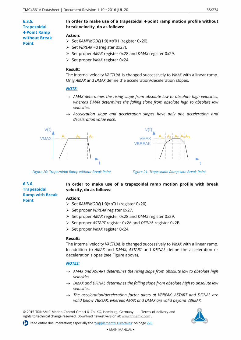
TMC4361A Datasheet | Document Revision 1.10 • 2016-JUL-20 35/234
© 2015 TRINAMIC Motion Control GmbH & Co. KG, Hamburg, Germany — Terms of delivery and
rights to technical change reserved. Download newest version at: www.trinamic.com .
Read entire documentation; especially the “Supplemental Directives” on page 228.
MAIN MANUAL
In order to make use of a trapezoidal 4-point ramp motion profile without break velocity, do as follows:
Action: Set RAMPMODE(1:0) =b’01 (register 0x20).
Set VBREAK =0 (register 0x27).
Set proper AMAX register 0x28 and DMAX register 0x29.
Set proper VMAX register 0x24.
Result: The internal velocity VACTUAL is changed successively to VMAX with a linear ramp.
Only AMAX and DMAX define the acceleration/deceleration slopes.
NOTE:
AMAX determines the rising slope from absolute low to absolute high velocities,
whereas DMAX determines the falling slope from absolute high to absolute low
velocities.
Acceleration slope and deceleration slopes have only one acceleration and
deceleration value each.
Figure 20: Trapezoidal Ramp without Break Point Figure 21: Trapezoidal Ramp with Break Point
In order to make use of a trapezoidal ramp motion profile with break velocity, do as follows:
Action: Set RAMPMODE(1:0)=b’01 (register 0x20).
Set proper VBREAK register 0x27.
Set proper AMAX register 0x28 and DMAX register 0x29.
Set proper ASTART register 0x2A and DFINAL register 0x2B.
Set proper VMAX register 0x24.
Result: The internal velocity VACTUAL is changed successively to VMAX with a linear ramp.
In addition to AMAX and DMAX, ASTART and DFINAL define the acceleration or
deceleration slopes (see Figure above).
NOTES:
AMAX and ASTART determines the rising slope from absolute low to absolute high
velocities.
DMAX and DFINAL determines the falling slope from absolute high to absolute low
velocities.
The acceleration/deceleration factor alters at VBREAK. ASTART and DFINAL are
valid below VBREAK, whereas AMAX and DMAX are valid beyond VBREAK.
v(t)
t
VMAXA1 A2 A3
v(t)
t
VMAX
VBREAK
A1 A2 A3LA1L A3
Trapezoidal 4-Point Ramp without Break Point
Trapezoidal Ramp with Break Point

TMC4361A Datasheet | Document Revision 1.10 • 2016-JUL-20 36/234
© 2015 TRINAMIC Motion Control GmbH & Co. KG, Hamburg, Germany — Terms of delivery and
rights to technical change reserved. Download newest version at: www.trinamic.com .
Read entire documentation; especially the “Supplemental Directives” on page 228.
MAIN MANUAL
Motion direction depends on XTARGET.
In order to use a 4-point or sixPoint ramps during positioning mode, do as follows:
Action:
Set RAMPMODE(2:0) =b’101 (register 0x20).
Set Trapezoidal ramp type accordingly, as explained above.
Set proper XTARGET register 0x37.
Result: The ramp finishes exactly at the target position XTARGET by keeping
|VACTUAL| = VMAX as long as possible.
AACTUAL assignments apply both for 4-point and sixPoint ramps.
The acceleration/deceleration factor AACTUAL register depends on the current
ramp phase and the velocity that needs to be reached. The related sign
assignment for different ramp phases is given in the following table:
Position Mode combined with Trapezoidal Ramps
AACTUAL Assignments for Trapezoidal Ramps
AACTUAL ASSIGNMENTS for Trapezoidal Ramps
Ramp phase: A1L A1 A2 A3 A3L
v>0: AACTUAL= ASTART AMAX 0 −DMAX −DFINAL
v<0: AACTUAL= −ASTART −AMAX 0 DMAX DFINAL
Table 16: Trapezoidal Ramps: AACTUAL Assignments during Motion

TMC4361A Datasheet | Document Revision 1.10 • 2016-JUL-20 37/234
© 2015 TRINAMIC Motion Control GmbH & Co. KG, Hamburg, Germany — Terms of delivery and
rights to technical change reserved. Download newest version at: www.trinamic.com .
Read entire documentation; especially the “Supplemental Directives” on page 228.
MAIN MANUAL
In order to make use of S-shaped ramps, do as follows:
Action: Set RAMPMODE(1:0)=b’10 (register 0x20).
Set proper BOW1 … BOW4 registers 0x2C…0x30.
Set proper AMAX register 0x28 and DMAX register 0x29.
Set ASTART = 0 (register 0x2A).
Set DFINAL = 0 (register 0x2B).
Set proper VMAX register 0x24.
Result: The internal velocity VACTUAL is changed successively to VMAX with S-shaped
ramps. The acceleration/deceleration values are altered on the basis of the bow
values.
Figure 22: S-shaped Ramp without initial and final Acceleration/Deceleration Values
Rising slope (absolute lower velocities to absolute higher velocities):
BOW1 determines the value which increases the absolute acceleration
value.
BOW2 determines the value which decreases the absolute acceleration
value.
AMAX determines the maximum acceleration value.
Falling slope (absolute higher velocities to absolute lower velocities):
BOW3 determines the value which increases the absolute deceleration
value.
BOW4 determines the value which decreases the absolute deceleration
value.
DMAX determines the maximum absolute deceleration value.
Description is continued on next page.
v(t)
t
VMAXB1 B12 B23 B34B3 B4B2
ASTART=0 DFINAL=0
Configuration of S-Shaped Ramps
Definition of Rising Slope for S-shaped Ramps
Definition of Falling Slope for S-shaped Ramps

TMC4361A Datasheet | Document Revision 1.10 • 2016-JUL-20 38/234
© 2015 TRINAMIC Motion Control GmbH & Co. KG, Hamburg, Germany — Terms of delivery and
rights to technical change reserved. Download newest version at: www.trinamic.com .
Read entire documentation; especially the “Supplemental Directives” on page 228.
MAIN MANUAL
Changing ramp parameters1 and/or operation mode during motion is not advised. However, if this is necessary, the following applies:
Avoid unintended system behavior during positioning mode!
Ramp parameter value changes during ramp progress can lead to:
A temporary overshooting of XTARGET or mechanical stop positions.
A temporary overshooting of VACTUAL beyond VMAX because the bows B1,
B2, B3, and B4 are maintained during the ramp progress.
This will ensure smooth operation during positioning mode.
1 Exceptions are XTARGET and VMAX. These Parameters can be changed during motion.
However, if it is necessary to change ramp parameters for S-shaped ramps during motion or to swtich from velocity to positioning mode, do as follows:
Action: Set or set again proper BOW3 registers 0x2F, regardless of wether the value
changes or not.
i Set this parameter after all other parameters have been set.
Result: Internal ramp calculations are reset through which the velocity ramp operates at
safe mode. During this mode, the target velocity is set to 0. In case the internal
ramp calculations are up-to-date, the ramp, which is configured by the actual
ramp parameters, is continued.
In order to configure S-shaped ramps with starting and finishing values for acceleration or deceleration, do as follows:
Action: Set RAMPMODE(1:0)=b’10 (register 0x20).
Set S-Shaped ramp as explained above (BOW1 … BOW4, AMAX, DMAX).
Set proper ASTART register 0x2A.
Set proper DFINAL register 0x2B.
Set proper VMAX register 0x24.
Result: The internal velocity VACTUAL is changed successively to VMAX with S-Shaped
ramps.
Figure 23: S-shaped Ramp with initial and final Acceleration/Deceleration Values
Description is continued on next page.
v(t)
t
VMAX
B1 B12 B23 B34B3 B4B2
ASTART>0 DFINAL>0
NOTICE
Changing Ramp Parameters during S-shaped Motion or Switching from Velocity to Positiong Mode
Configuration of S-shaped Ramp with ASTART and DFINAL

TMC4361A Datasheet | Document Revision 1.10 • 2016-JUL-20 39/234
© 2015 TRINAMIC Motion Control GmbH & Co. KG, Hamburg, Germany — Terms of delivery and
rights to technical change reserved. Download newest version at: www.trinamic.com .
Read entire documentation; especially the “Supplemental Directives” on page 228.
MAIN MANUAL
The acceleration/deceleration values are altered, based on the bow values.
The start phase and the end phase of an S-shaped ramp is
accelerated/decelerated by ASTART and DFINAL.
The ramp starts with ASTART and stops with DFINAL.
DFINAL becomes valid when AACTUAL reaches the chosen DFINAL value.
i The parameter DFINAL is not considered during positioning mode.
AACTUAL assignments and current bow value selection for S-shaped ramps.
The acceleration/deceleration factor depends on the current ramp phase and
alters every 64 clock cycles during the bow phases B1, B2, B3, and B4.
Details are provided in the table below:
RAMPMODE(2:0) =b’110
The ramp finishes exactly on target position; keeping |VACTUAL| = VMAX as
long as possible until the ramp falls to reach XTARGET exactly.
It is possible that the phases B12, B23, and B34 are left out due to given
values. Therefore, the highest speed performance is possible due to a
maximum speed positioning ramp.
The fastest possible slopes are always performed if the phases B12 and/or
B34 are not reached during a rising and/or falling S-shaped slope.
The ramp maintains the maximum velocity VMAX as long as possible in
positioning mode until the falling slope finishes the ramp to reach XTARGET
exactly. The result is the fastest possible positioning ramp in matters of
time.
Definitions for S-shaped Ramps
AACTUAL Assignments for S-shaped Ramps
S-shaped Ramps: Assignments for AACTUAL and Internal Bow Value
Ramp phase: B1 B12 B2 B23 B3 B34 B4
v>0: AACTUAL= ASTARTàAMAX AMAX AMAXà0 0 0à-DMAX -DMAX -DMAXà-DFINAL
BOWACTUAL= BOW1 0 -BOW2 0 -BOW3 0 BOW4
v<0: AACTUAL= -ASTARTà-AMAX -AMAX -AMAXà0 0 0àDMAX DMAX DMAXàDFINAL
BOWACTUAL= -BOW1 0 BOW2 0 BOW3 0 -BOW4
Table 17: Parameter Assignments for S-shaped Ramps
S-shaped Mode and Positioning: Fast Motion

TMC4361A Datasheet | Document Revision 1.10 • 2016-JUL-20 40/234
© 2015 TRINAMIC Motion Control GmbH & Co. KG, Hamburg, Germany — Terms of delivery and
rights to technical change reserved. Download newest version at: www.trinamic.com .
Read entire documentation; especially the “Supplemental Directives” on page 228.
MAIN MANUAL
Start Velocity VSTART and Stop Velocity VSTOP
S-shaped and trapezoidal velocity ramps can be configured with unsigned start and stop velocity values: VSTART, or VSTOP. Per default, VSTART and VSTOP are set to 0. The sign is selected automatically, depending on the current ramp status and the target velocity, or target position. This section explains how to set up the respective values correctly.
S-shaped and trapezoidal velocity ramps can be started with an initial velocity
value, if you set the VSTART value higher than zero (see Figure below).
In order to use trapezoidal ramps with an initial start velocity, do as follows:
Action: Set RAMPMODE(1:0)=b’01 (register 0x20).
Set Trapezoidal ramp type accordingly, as explained before.
Set proper VSTART > 0 (register 0x25).
Set VSTOP = 0 (register 0x26).
Result: The trapezoidal ramp starts with initial velocity.
NOTE:
The initial acceleration value is AMAX if VBREAK < VSTART, otherwise the starting
acceleration value is ASTART.
Figure 24: Trapezoidal Ramp with initial Velocity
If trapezoidal ramp with initial velocity VSTART is selected:
Avoid unintended system behavior during positioning mode!
Use VSTART without setting VSTOP > VSTART only in positioning mode if there
is enough distance between the current position XACTUAL and the target
position XTARGET.
This will ensure smooth operation during positioning mode.
Turn page for information on how to configure S-shaped ramps with initial start
velocity.
v(t)
t
VMAX
VBREAK
A1 A2 A3LA1L A3
VSTART
Starting Ramps with initial Velocity
NOTICE

TMC4361A Datasheet | Document Revision 1.10 • 2016-JUL-20 41/234
© 2015 TRINAMIC Motion Control GmbH & Co. KG, Hamburg, Germany — Terms of delivery and
rights to technical change reserved. Download newest version at: www.trinamic.com .
Read entire documentation; especially the “Supplemental Directives” on page 228.
MAIN MANUAL
In order to use S-shaped ramps with initial start velocity, do as follows:
Action:
Set RAMPMODE(1:0)=b’10 (register 0x20).
Set S-shaped ramp type accordingly, as explained before.
Set proper VSTART > 0 (register 0x25).
Set VSTOP = 0 (register 0x26).
Result: The S-shaped ramp starts with initial velocity.
PRINCIPLE:
The initial acceleration value is equal to AMAX. The parameter ASTART is not
considered. Consequently, ramp phase B1 is not performed.
Figure 25: S-shaped Ramp with initial Start Velocity
If S-shaped ramp with initial velocity VSTART is selected:
Avoid unintended system behavior during positioning mode!
Keep in mind that the S-shaped character of the curve is maintained.
Because AMAX is the start acceleration value, the ramp will always execute
phase B2 which could result in positioning overshoots.
Use VSTART only in positioning mode if there is enough distance between
the current position XACTUAL and the target position XTARGET.
This will ensure smooth operation during positioning mode.
Turn page for information on how to configure finishing ramps with stop velocity.
v(t)
t
VMAXB1 B12 B23 B34B3 B4B2
VSTART
S-shaped Ramps with initial Start Velocity
NOTICE

TMC4361A Datasheet | Document Revision 1.10 • 2016-JUL-20 42/234
© 2015 TRINAMIC Motion Control GmbH & Co. KG, Hamburg, Germany — Terms of delivery and
rights to technical change reserved. Download newest version at: www.trinamic.com .
Read entire documentation; especially the “Supplemental Directives” on page 228.
MAIN MANUAL
S-shaped and trapezoidal velocity ramps can be finished with a stop velocity value
if you set VSTOP value higher than zero (see figure below).
In order to configure trapezoidal ramps with stop velocity, do as follows:
Action: Set RAMPMODE(1:0)=b’01 (register 0x20).
Set Trapezoidal ramp type accordingly, as explained before.
Set VSTART = 0 (register 0x25).
Set proper VSTOP > 0 (register 0x26).
Result: The trapezoidal ramp stops with defined velocity.
Figure 20: Trapezoidal Ramp with Stop Velocity
If trapezoidal ramps are selected (VBREAK > 0):
Avoid unintended system behavior during positioning mode!
Set VBREAK > VSTOP.
Set VSTART < VSTOP.
This will ensure smooth operation during positioning mode.
Turn page for configuration information on S-shaped ramps with stop velocity.
v(t)
t
VMAX
VBREAK
A1 A2 A3LA1L A3
VSTOP
Finishing Ramps with Stop Velocity
NOTICE

TMC4361A Datasheet | Document Revision 1.10 • 2016-JUL-20 43/234
© 2015 TRINAMIC Motion Control GmbH & Co. KG, Hamburg, Germany — Terms of delivery and
rights to technical change reserved. Download newest version at: www.trinamic.com .
Read entire documentation; especially the “Supplemental Directives” on page 228.
MAIN MANUAL
In order to use S-shaped ramps with stop velocity, do as follows:
Action: Set RAMPMODE(1:0)=b’10 (register 0x20).
Set S-shaped ramp type accordingly, as explained before.
Set VSTART = 0 (register 0x25).
Set proper VSTOP > 0 (register 0x26).
Result: The S-shaped ramp finishes with stop velocity.
NOTE:
The final deceleration value is equal to DMAX. The parameter DFINAL is not
considered. Consequently, ramp phase B4 is not performed.
Figure 26: S-shaped Ramp with Stop Velocity
Interaction of VSTART, VSTOP, VACTUAL and VMAX:
VSTOP can be used in positioning mode, if the target position is reached. In
velocity mode, VSTOP is also used if VACTUAL ≠ 0 and the target velocity
VMAX is assigned to 0.
VSTART and VSTOP are not only used to start or end a velocity ramp. If the
velocity direction alters due to register assignments while a velocity ramp is
in progress, the velocity values develop according to the current velocity
ramp type, using VSTART or VSTOP.
The unsigned values VSTART and VSTOP are valid for both velocity directions.
Every register value change is assigned immediately.
Turn page for information on how to configure S-shaped ramps with start and stop
velocity.
v(t)
t
VMAXB1 B12 B23 B34B3 B4B2
VSTOP
S-shaped Ramps with Stop Velocity

TMC4361A Datasheet | Document Revision 1.10 • 2016-JUL-20 44/234
© 2015 TRINAMIC Motion Control GmbH & Co. KG, Hamburg, Germany — Terms of delivery and
rights to technical change reserved. Download newest version at: www.trinamic.com .
Read entire documentation; especially the “Supplemental Directives” on page 228.
MAIN MANUAL
S-shaped ramps can be configured with a combination of VSTART and VSTOP.
It is possible to include both processes in one S-Shaped ramp to decrease the time
between start and stop of the ramp.
In order to use S-Shaped ramps with a combination of start and stop velocity, do as follows:
Action:
Set RAMPMODE(1:0)=b’10.
Set S-shaped ramp type accordingly, as explained before, but with
BOW2 ≠ BOW4.
Set proper VSTART > 0 (register 0x25).
Set proper VSTOP > 0 (register 0x26).
Result:
The S-shaped ramp starts with initial velocity and stops with defined velocity.
Figure 27: S-shaped Ramp with Start and Stop Velocity
If S-shaped ramp with initial velocity VSTART and stop velocity VSTOP is selected:
Avoid unintended system behavior during positioning mode!
Keep in mind that the S-shaped character of the curve is maintained.
Because AMAX is the start acceleration value, the ramp will always execute
phase B2, which could result in positioning overshoots.
Use VSTART in positioning mode, if there is enough distance between the
current position XACTUAL and the target position XTARGET.
This will ensure smooth operation during positioning mode.
Turn page for information on how to use VSTART and ASTART for S-shaped ramps.
v(t)
t
VMAXB1 B12 B23 B34B3 B4B2
VSTOPVSTART
S-shaped Ramps with Start and Stop Velocity
NOTICE

TMC4361A Datasheet | Document Revision 1.10 • 2016-JUL-20 45/234
© 2015 TRINAMIC Motion Control GmbH & Co. KG, Hamburg, Germany — Terms of delivery and
rights to technical change reserved. Download newest version at: www.trinamic.com .
Read entire documentation; especially the “Supplemental Directives” on page 228.
MAIN MANUAL
For some S-shaped ramp applications it can be useful to start with a defined
velocity value (VSTART > 0);but not with the maximum acceleration value AMAX.
In order to start with a defined velocity value, do as follows:
Action: Set RAMPMODE(1:0) =b’10 (register 0x20).
Set S-shaped ramp type accordingly, as explained before.
Set proper VSTART > 0 (register 0x25).
Set proper VSTOP > 0 (register 0x26).
Set use_astart_and_vstart =1 (bit0 of the GENERAL_CONF register 0x00).
Result:
The following special ramp types can be generated in this way, as shown below.
i Section B1 is passed through although VSTART is used.
Using VSTART and starting acceleration of 0
for S-shaped ramps
Using VSTART and starting acceleration,
which is smaller than AMAX for S-shaped ramps
Figure 28: S-shaped Ramps with combined VSTART and ASTART Parameters
If S-shaped ramp with VSTART, ASTART, and VSTOP is selected:
Avoid unintended system behavior during positioning mode!
Keep in mind that the S-shaped character of the curve is maintained.
Because ASTART is the start acceleration value, the ramp will always execute
phase B2, which could result in positioning overshoots.
Use VSTART and ASTART > 0 without setting VSTOP > VSTART only in
positioning mode, if there is enough distance between the current position
XACTUAL and the target position XTARGET.
This will ensure smooth operation during positioning mode.
v(t)
VMAXB1 B12 B23 B34B3 B4B2
VSTOP
VSTART
aSTART = 0
v(t)
t
VMAXB1 B12 B23 B34B3 B4B2
VSTOP
VSTART
aSTART > 0
Combined Use of VSTART and ASTART for
S-shaped Ramps
NOTICE

TMC4361A Datasheet | Document Revision 1.10 • 2016-JUL-20 46/234
© 2015 TRINAMIC Motion Control GmbH & Co. KG, Hamburg, Germany — Terms of delivery and
rights to technical change reserved. Download newest version at: www.trinamic.com .
Read entire documentation; especially the “Supplemental Directives” on page 228.
MAIN MANUAL
sixPoint Ramps
sixPoint ramps are trapezoidal ramps with initial and stop velocity values that also make use of two acceleration and two deceleration values.
sixPoint ramps are trapezoidal velocity ramps that can be configured with a
combination of VSTART and VSTOP.
In order to use trapezoidal ramps with a combination of start and stop velocity, do as follows:
Action:
Set RAMPMODE(1:0)=b’01 (register 0x20).
Set a Trapezoidal ramp type appropriately as explained before.
Set proper VSTART > 0 (register 0x25).
Set proper VSTOP > 0 (register 0x26).
Set proper VBREAK > 0 (register 0x27).
Result: The sixPoint ramp starts with an initial velocity and stops with a defined velocity.
v(t)
t
VMAX
VBREAK
A1 A2 A3LA1L A3
VSTOPVSTART
Figure 29: sixPoint Ramp: Trapezoidal Ramp with Start and Stop Velocity
If a sixPoint ramp is used:
Avoid unintended system behavior during positioning mode!
Set VBREAK > VSTOP.
Set VSTART < VSTOP.
This will ensure smooth operation during positioning mode.
Configuration of sixPoint Ramps
Diagram of sixPoint Ramp
NOTICE

TMC4361A Datasheet | Document Revision 1.10 • 2016-JUL-20 47/234
© 2015 TRINAMIC Motion Control GmbH & Co. KG, Hamburg, Germany — Terms of delivery and
rights to technical change reserved. Download newest version at: www.trinamic.com .
Read entire documentation; especially the “Supplemental Directives” on page 228.
MAIN MANUAL
U-Turn Behavior
The process that is triggered when motion direction changes during motion, is described below, and applies to all ramp types.
In case the motion direction is changed during motion in velocity mode (by direct
assignment of VMAX) or in positioning mode (due to XTARGET reassignment), the
following process is triggered:
1. Motion is directed to VACTUAL = 0.
i If VSTOP is used (≠ 0), motion terminates at VSTOP.
2. A standstill phase of TZEROWAIT clock cycles (register 0x7B) occurs.
i It is recommended to assign TZEROWAIT > 0, if VSTOP and/or a
trapezoidal ramp type are used, because motor oscillations can occur
that must peter out.
3. Motion continues to the actual XTARGET (positioning mode), or to the newly
assigned VMAX (velocity mode).
i If VSTART is used (≠ 0), motion begins with VSTART if TZEROWAIT > 0.
After reaching VSTOP, TZEROWAIT clock cycles are waited until motion continues to
peter out motor oscillations.
Figure 30: Example for U-Turn Behavior of sixPoint Ramp
Turn page for information on U-Turn for S-shaped ramps.
v(t)
t
VMAX
VBREAK
VSTOP
VSTART
-VMAX
-VBREAK
-VSTOP
-VSTART
TZEROWAIT
U-Turn Behavior
Example: U-Turn for sixPoint Ramps

TMC4361A Datasheet | Document Revision 1.10 • 2016-JUL-20 48/234
© 2015 TRINAMIC Motion Control GmbH & Co. KG, Hamburg, Germany — Terms of delivery and
rights to technical change reserved. Download newest version at: www.trinamic.com .
Read entire documentation; especially the “Supplemental Directives” on page 228.
MAIN MANUAL
When VACTUAL = 0 is reached, motion immediately continues. In most S-shaped
ramp applications that do not use VSTOP, a standstill phase is not required.
If ASTART > 0 and/or DFINAL > 0, these parameters are also used during U-Turn.
Figure 31: Example for U-Turn Behavior of S-shaped Ramp
There is one exception to the above explained U-Turn process:
In case BOW2 equals BOW4, the S-shaped ramp is not stopped at VACTUAL = 0.
While passing VACTUAL = 0, motion acceleration does not equal 0. Thus, the fastest
possible U-Turn behavior for this ramp is created.
In the figure below, this velocity ramp behavior is depicted as bold black line,
whereas the velocity ramp behavior of the process explained above is depicted
gray line:
Figure 32: Direct transition via VACTUAL=0 for S-shaped Ramps
v(t)
t
-VMAX
-VMAX
TZEROWAIT
=0
v(t)
t
-VMAX
-VMAX
BOW2=BOW4!
Example: U-Turn for S-shaped Ramps
Continuous Velocity Motion Profile for S-shaped Ramps

TMC4361A Datasheet | Document Revision 1.10 • 2016-JUL-20 49/234
© 2015 TRINAMIC Motion Control GmbH & Co. KG, Hamburg, Germany — Terms of delivery and
rights to technical change reserved. Download newest version at: www.trinamic.com .
Read entire documentation; especially the “Supplemental Directives” on page 228.
MAIN MANUAL
Internal Ramp Generator Units
This section provides information about the arithmetical units of the ramp parameters.
All parameter units are real arithmetical units.
Therefore, it is necessary to set the CLK_FREQ register 0x31 to proper [Hz] value,
which is defined by the external clock frequency fCLK. Any value between
fCLK = 4.2 MHz and 32 MHz can be selected.
Default configuration is 16 MHz.
Velocity values are always defined as pulses per second [pps].
VACTUAL is given as a 32-bit signed value with no decimal places. The unsigned
velocity values VSTART, VSTOP, and VBREAK consist of 23 digits and 8 decimal
places. VMAX is a signed value with 24 digits and 8 decimal places.
The maximum velocity VMAX is restricted as follows:
VMAX ≤ ½ pulse · fCLK
NOTE:
In case VACTUAL exceeds this limit INCORRECT step pulses at STPOUT output occur.
The unsigned values AMAX, DMAX, ASTART, DFINAL, and DSTOP consist of 22 digits
and 2 decimal places.
AACTUAL shows a 32-bit nondecimal signed value. Acceleration and deceleration
units are defined per default as pulses per second² [pps²].
If higher acceleration/deceleration values are required for short and steep ramps, do as follows:
Action: Set direct_acc_val_en =1 (GENERAL_CONF register 0x00).
Result: The parameters are defined as velocity value change per clock cycle with 24-bit
unsigned decimal places (MSB =2-14). The values are calculated as follows:
AMAX [pps2] = AMAX / 237 · fCLK2
DMAX [pps2] = DMAX / 237 · fCLK2
ASTART [pps2] = ASTART / 237 · fCLK2
DFINAL [pps2] = DFINAL / 237 · fCLK2
DSTOP [pps2] = DSTOP / 237 · fCLK2
The maximum acceleration or deceleration values, in case direct_acc_val_en is activated, are as follows:
AMAX ≤ 65535
DMAX ≤ 65535
ASTART ≤ 65535
DFINAL ≤ 65535
DSTOP ≤ 65535
Continued on next page.
Clock Frequency
Velocity Value Units
Acceleration Value Units
TMC4361A Datasheet | Document Revision 1.10 • 2016-JUL-20 50/234
© 2015 TRINAMIC Motion Control GmbH & Co. KG, Hamburg, Germany — Terms of delivery and
rights to technical change reserved. Download newest version at: www.trinamic.com .
Read entire documentation; especially the “Supplemental Directives” on page 228.
MAIN MANUAL
Bow values BOW1…BOW4: Bow values are unsigned 24-bit values without decimal places. They are defined
per default as pulses per second³ [pps³].
In case higher bow values are required for short and steep ramps, do as follows:
Action: Set direct_bow_val_en =1 (GENERAL_CONF register 0x00)
Result: The parameters are defined as acceleration value change per clock cycle with
24-bit unsigned decimal places with the MSB defined as 2-29.
The particular bow values BOW1, BOW2, BOW3, BOW4 are calculated as follows:
BOWx [pps3] = BOWx / 253 · fCLK3
The maximum bow values, in case direct_acc_val_en is activated, are as follows:
BOW1…4 ≤ 4095
Overview of Minimum and Maximum Values:
Minimum and Maximum Values (Frequency Mode)
Value Classes Velocity Acceleration Bow Clock
Affected Registers VMAX, VSTART,
VSTOP, VBREAK
AMAX, DMAX,
ASTART, DFINAL
BOW1, BOW2,
BOW3, BOW4 CLK_FREQ (fCLK)
Minimum value 3.906 mpps 0.25 mpps2 1 mpps3 4.194 MHz
Maximum value
8.388 Mpps
and
½ pulse · fCLK
4.194 Mpps2 16.777 Mpps3 32 MHz
Table 18: Minimum and Maximum Values if Real World Units are selected
Minimum and Maximum Values for Steep Slopes (Direct Mode, example with fCLK =16MHz)
Value Classes Acceleration (direct_acc_val_en =1) Bow (direct_bow_val_en =1)
Affected Registers AMAX, DMAX, ASTART, DFINAL, DSTOP BOW1, BOW2, BOW3, BOW4
Value restrictions: < 65536 < 4096
Calculation a[pps²] = (∆v/clk_cycle) / 237 · fCLK2 bow[pps³] = (∆a/clk_cycle) / 253 · fCLK
3
Minimum value ~1.86 kpps² ~454.75 kpps³
Maximum value ~122.07 Mpps² ~1.86 Gpps3
Table 19: Minimum and Maximum Values for Steep Slopes for fCLK =16MHz
Bow Value Units

TMC4361A Datasheet | Document Revision 1.10 • 2016-JUL-20 51/234
© 2015 TRINAMIC Motion Control GmbH & Co. KG, Hamburg, Germany — Terms of delivery and
rights to technical change reserved. Download newest version at: www.trinamic.com .
Read entire documentation; especially the “Supplemental Directives” on page 228.
MAIN MANUAL
7. External Step Control and Electronic Gearing
Steps can also be generated by external steps that are manipulated internally by an electronic gearing process. In the following chapter, steps generation by external control and electronic gearing is presented.
Pins for External Step Control Pin Names Type Remarks
STPIN Input Step input signal.
DIRIN Input Direction input signal.
Table 20: Pins used for External Step Control
Registers used for external Step Control
Register Name Register Address Remarks
GENERAL_CONF 0x00 RW Bits 9:6, 26.
GEAR_RATIO 0x12 RW Electronic gearing factor; signed;
32 bits=8+24 (8-bit digits, 24-bit decimal places).
Table 21: Registers used for External Step Control
In order to synchronize with other motion controllers, TMC4361A offers a step
direction input interface at the STPIN and DIRIN input pins.
i Three options are available. In case one of these options is selected, the
internal step generator is disabled.
OPTION 1: HIGH ACTIVE EXTERNAL STEPS
Action: Set sdin_mode = b’01 (GENERAL_CONF register 0x00).
Result: As soon as the STPIN input signal switches to high state the control unit recognizes
an external step.
OPTION 2: LOW ACTIVE EXTERNAL STEPS
Action: Set sdin_mode = b’10 (GENERAL_CONF register 0x00).
Result: As soon as the STPIN input signal switches to low state the control unit recognizes
an external step.
OPTION 3: TOGGLING EXTERNAL STEPS
Action: Set sdin_mode = b’11 (GENERAL_CONF register 0x00).
Result: As soon as the STPIN input signal switches to low or high state the control unit
recognizes an external step.
Continued on next page.
Enabling External Step Control

TMC4361A Datasheet | Document Revision 1.10 • 2016-JUL-20 52/234
© 2015 TRINAMIC Motion Control GmbH & Co. KG, Hamburg, Germany — Terms of delivery and
rights to technical change reserved. Download newest version at: www.trinamic.com .
Read entire documentation; especially the “Supplemental Directives” on page 228.
MAIN MANUAL
DIRIN polarity can be assigned. Per default, the negative direction is indicated by
DIRIN = 0.
In order to change this polarity:
Action: Set pol_dir_in = 1 (GENERAL_CONF register 0x00).
Result: A negative input direction is assigned by DIRIN = 1.
If an external step is not congruent with an internal step, the GEAR_RATIO register
0x12 must be set accordingly. This signed parameter consists of eight bit digits
and 24 bits decimal places.
With every external step the assigned GEAR_RATIO value is added to an internal
accumulation register. As soon as an overflow occurs, an internal step is
generated and the remainder will be kept for the next external step.
Any absolute gearing value between 2-24 and 127 is possible.
NOTE:
Gearing ratios beyond 1 are more reasonable for the SPI output. The internal
SinLUTable is used that generates multiple steps one after another without
interpolation, if the accumulation register value is above 1. In contrast to a burst
of steps at the STPOUT pin, the SPI output will only forward the new position in the
inner SinLUT where only some values have been skipped if |GEAR_RATIO|>1.
A negative gearing factor GEAR_RATIO < 0 inverts the interpretation of the input
direction which is determined by DIRIN and pol_dir_in.
It is possible to use the internal ramp generator in combination with the external
S/D interface.
In this case, the external step impulses transferred via STPIN and DIRIN cannot
influence the internal XACTUAL counter directly. Instead, the XTARGET register is
altered by 1 or -1 with every GEAR_RATIO accumulation register overflow.
NOTE:
Whether XTARGET is increased or decreased is determined similarly to the direct
electronic gearing control. The accumulation register overflow direction indicates
the target alteration. Respectively, the accumulation direction is determined by the
GEAR_RATIO sign, by pol_dir_in, and by DIRIN.
Consecutive input steps must occur with a distance of minimum 64 clock cycles.
i This feature allows a synchronized motion of different positioning ramps for
different TMC4361A chips with differently configured ramps.
In order to select indirect external control, do as follows:
Action: Set sdin_mode ≠ b’00 according to the required external control option.
Set sd_indirect_control = 1 (GENERAL_CONF register 0x00).
Result: As soon as an external step is generated, XTARGET is increased or decreased,
according to the accumulation direction.
Selecting the Input Direction Polarity
Description of Electronic Gearing
Indirect External Control

TMC4361A Datasheet | Document Revision 1.10 • 2016-JUL-20 53/234
© 2015 TRINAMIC Motion Control GmbH & Co. KG, Hamburg, Germany — Terms of delivery and
rights to technical change reserved. Download newest version at: www.trinamic.com .
Read entire documentation; especially the “Supplemental Directives” on page 228.
MAIN MANUAL
In some cases, it is useful to switch from external to internal ramp generation
during motion.
TMC4361A supports a smooth transfer from direct external control to an internal
ramp. The only parameter you need to know and apply is the current velocity
when the switching occurs. In more detail, this means that when the external
control is switched off, VSTART takes over the definition of the actual velocity value.
The ramp direction is then selected automatically. The time step of the last
internal step is also taken into account in order to provide a smooth transition
from external to internal ramp control.
In order to select automatic switching from external to internal control, do as follows:
PRECONDITION (EXTERNAL DIRECT CONTROL IS ACTIVE):
Action: Set sdin_mode ≠ b’00 (GENERAL_CONF register 0x00).
Set sd_indirect_control = 0 (GENERAL_CONF register 0x00).
Set ASTART = 0 (register 0x2A).
PROCEED WITH:
Action: Set automatic_direct_sdin_switch_off = 1 (GENERAL_CONF register 0x00) once
before switching to internal control.
Continually adapt VSTART register 0x25 according to the actual velocity of the
TMC4361A that must be calculated in the µC.
If switching must be prompted, set sdin_mode = b’00.
Result: The internal ramp velocity is started with the value of VSTART, and the direction is
set automatically on the basis of the external steps that have occurred before.
Turn page for information on how configure smooth switching for S shaped ramps.
Switching from External to Internal Control

TMC4361A Datasheet | Document Revision 1.10 • 2016-JUL-20 54/234
© 2015 TRINAMIC Motion Control GmbH & Co. KG, Hamburg, Germany — Terms of delivery and
rights to technical change reserved. Download newest version at: www.trinamic.com .
Read entire documentation; especially the “Supplemental Directives” on page 228.
MAIN MANUAL
In order to also support a smooth S-shaped ramp transition - when the external
step control is switched off - the starting acceleration value can also be set
separately at ASTART register 0x2A.
i In contrast to the automatic direction assignment, the sign of ASTART must be
set manually.
In order to select automatic switching from external to internal control with a starting acceleration value, do as follows:
PRECONDITION (EXTERNAL DIRECT CONTROL IS ACTIVE):
Action: Set sdin_mode ≠ b’00 (GENERAL_CONF register 0x00).
Set sd_indirect_control = 0 (GENERAL_CONF register 0x00).
PROCEED WITH:
Action: Set automatic_direct_sdin_switch_off = 1 once before switching to internal
control.
Continually adapt VSTART register 0x25 according to the actual velocity of the
TMC4361A — that must be calculated in the µC.
Continually adapt ASTART according to the actual acceleration (unsigned value)
of the TMC4361A — that must be calculated in the µC.
Continually set ASTART(31) = 0 or 1 according to the current acceleration
direction.
If switching must be prompted, set sdin_mode = b’00.
Result: The internal ramp velocity is started with the value of VSTART, and the direction is
set automatically on the basis of the external steps that have occurred before.
The internal acceleration value is set to:
+ASTART if ASTART(31) = 0 or
–ASTART if ASTART(31) = 1.
Smooth Switching for S-shaped Ramps

TMC4361A Datasheet | Document Revision 1.10 • 2016-JUL-20 55/234
© 2015 TRINAMIC Motion Control GmbH & Co. KG, Hamburg, Germany — Terms of delivery and
rights to technical change reserved. Download newest version at: www.trinamic.com .
Read entire documentation; especially the “Supplemental Directives” on page 228.
MAIN MANUAL
8. Reference Switches
The reference input signals of the TMC4361A function partly as safety features. The TMC4361A provides a range of reference switch settings that can be configured for many different applications. The TMC4361A offers two hardware switches (STOPL, STOPR) and two additional virtual stop switches (VIRT_STOP_LEFT, VIRT_STOP_RIGHT). A home reference switch HOME_REF is also available.
Pins used for Reference Switches
Pin Names Type Remarks
STOPL Input Left reference switch.
STOPR Input Right reference switch.
HOME_REF Input Home switch.
TARGET_REACHED Output Reference switch to indicate XACTUAL=XTARGET.
Table 22: Pins used for Reference Switches
Dedicated Registers for Reference Switches
Register Name Register Address Remarks
REFERENCE_CONF 0x01 RW Configuration of interaction with reference pins.
HOME_SAFETY_MARGIN 0x1E RW Region of uncertainty around X_HOME.
DSTOP 0x2C RW
Deceleration value if stop switches STOPL / STOPR or
virtual stops are used with soft stop ramps. The
deceleration value allows for an automatic linear stop
ramp.
POS_COMP 0x32 RW Free configurable compare position; signed; 32 bits.
VIRT_STOP_LEFT 0x33 RW Virtual left stop that triggers a stop event at
XACTUAL ≤ VIRT_STOP_LEFT; signed; 32 bits.
VIRT_STOP_RIGHT 0x34 RW Virtual left stop that triggers a stop event at
XACTUAL ≥ VIRT_STOP_RIGHT; signed; 32 bits.
X_HOME 0x35 RW Home reference position; signed; 32 bits.
X_LATCH 0x36 RW Stores XACTUAL at different conditions; signed; 32
bits.
Table 23: Dedicated Registers for Reference Switches

TMC4361A Datasheet | Document Revision 1.10 • 2016-JUL-20 56/234
© 2015 TRINAMIC Motion Control GmbH & Co. KG, Hamburg, Germany — Terms of delivery and
rights to technical change reserved. Download newest version at: www.trinamic.com .
Read entire documentation; especially the “Supplemental Directives” on page 228.
MAIN MANUAL
Hardware Switch Support
The TMC4361A offers two hardware switches that can be configured according to your design.
The hardware provides a left and a right stop in order to stop the drive
immediately in case one of them is triggered. Therefore, pin 12 and pin 14 of the
motion controller must be used.
NOTE:
Both switches must be enabled before motion occurs.
In order to enable STOPL correctly, do as follows:
Action: Determine the active polarity voltage of STOPL and set pol_stop_left
(REFERENCE_CONF register 0x01) accordingly.
Set stop_left_en =1 (REFERENCE_CONF register 0x01).
Result: The current velocity ramp stops in case the STOPL voltage level matches
pol_stop_left and VACTUAL < 0.
In order to enable STOPR correctly, do as follows:
Action: Determine the active polarity voltage of STOPR and set pol_stop_right
(REFERENCE_CONF register 0x01) accordingly.
Set stop_right_en =1 (REFERENCE_CONF register 0x01).
Result: The current velocity ramp stops in case STOPR voltage level matches pol_stop_right
and VACTUAL > 0.
The stop slope can be configured for hard or linear stop slopes. Per default, hard
stops are selected.
If hard stops are required, do as follows:
OPTION 1: HARD STOP SLOPES
Action: Set soft_stop_en =0 (REFERENCE_CONF register 0x01).
Result: If one of the stop switches is active and enabled, the velocity ramp is set
immediately to VACTUAL = 0.
OPTION 2: LINEAR STOP SLOPES
If linear stop ramps are required:
Action: Set proper DSTOP > max(DMAX; DFINAL) (register 0x2C).
Set soft_stop_en =1 (REFERENCE_CONF register 0x01).
Result: If one of the stop switches is active and enabled, the velocity ramp is stopped with
a linear deceleration slope until VACTUAL = 0 is reached. In this case the
deceleration factor is determined by DSTOP. VSTOP is not considered during the
stop deceleration slope.
STOPL and STOPR
Stop Slope Configuration for Hard or Linear Stop Slopes

TMC4361A Datasheet | Document Revision 1.10 • 2016-JUL-20 57/234
© 2015 TRINAMIC Motion Control GmbH & Co. KG, Hamburg, Germany — Terms of delivery and
rights to technical change reserved. Download newest version at: www.trinamic.com .
Read entire documentation; especially the “Supplemental Directives” on page 228.
MAIN MANUAL
When a stop switch becomes active the related status flag is set in the STATUS flags
register 0x0F. The flag remains active as long as the stop switch remains active.
The particular event is also released in the EVENTS register 0x0E, which remains
active until the event bit is reset manually. When VACTUAL = 0 is reached after the
stop event no motion toward this particular direction is possible.
In order to move into the locked direction, the following is required:
PRECONDITION 1:
The particular stop switch is NOT active anymore.
AND/OR
PRECONDITION 2: The stop switch is disabled (stop_left/right_en = 0).
Action: Set back the active event by reading out the EVENTS register 0x0E.
i There is only one exception to this: If an event is selected for the
EVENT_CLEAR_CONF register in order to inhibit the regular clearing. See
information provided in Chapter 5, Page 24.
Result: The active stop event is reset to free motion into the locked direction.
It is possible to select four different events to store the current internal position
XACTUAL in the register X_LATCH.
The table below show which transition of the reference signal leads to the X_LATCH
transfer. For each transition process the specified reference configurations in the
REFERENCE_CONF register 0x01 must be set accordingly.
If you need to change the directions of the reference switches, do as follows:
Action: Set invert_stop_direction=1 (REFERENCE_CONF register 0x01).
Result: STOPL is now the right reference switch and STOPR is now the left reference
switch. Consequently, all configuration parameters for STOPL become valid for
STOPR and vice versa.
How Active Stops are indicated and reset to Free Motion
How to latch Internal Position on Switch Events
Reference Configuration pol_stop_left=0 pol_stop_left=1 pol_stop_right=0 pol_stop_right=1
latch_x_on_inactive_l=1 STOPL=0 à 1 STOPL=1 à 0 --- ---
latch_x_on_active_l=1 STOPL=1 à 0 STOPL=0 à 1 --- ---
latch_x_on_inactive_r=1 --- --- STOPR=0 à 1 STOPR = 1à0
latch_x_on_active_r=1 --- --- STOPR=1 à 0 STOPR = 0à1
Table 24: Reference Configuration and Corresponding Transition of particular Reference Switch
Interchange the Reference Switches without Physical Reconnection

TMC4361A Datasheet | Document Revision 1.10 • 2016-JUL-20 58/234
© 2015 TRINAMIC Motion Control GmbH & Co. KG, Hamburg, Germany — Terms of delivery and
rights to technical change reserved. Download newest version at: www.trinamic.com .
Read entire documentation; especially the “Supplemental Directives” on page 228.
MAIN MANUAL
Virtual Stop Switches
TMC4361A provides additional virtual limits; which trigger stop slopes in case the specific virtual stop switch microstep position is reached. Virtual stop positions are assigned using the VIRTUAL_STOP_LEFT register 0x33 and VIRTUAL_STOP_RIGHT register 0x34. In this section, configuration details for virtual stop switches are provided for various design-in purposes. NOTE:
Virtual stop switches must be enabled in the same manner as nonvirtual reference switches. Hitting a
virtual limit switch - by receiving the assigned position - triggers the same process as hitting STOPL or
STOPR.
In order to enable left virtual stop correctly, do as follows:
Action: Set VIRTUAL_STOP_LEFT register 0x33 according to left stop position.
Set virtual_left_limit_en =1 (REFERENCE_CONF register 0x01).
Result: The actual velocity ramp stops in case XACTUAL ≤ VIRT_STOP_LEFT. The ramp is
stopped according to the selected ramp type.
In order to enable right virtual stop correctly, do as follows:
Action: Set VIRTUAL_STOP_RIGHT register 0x34 according to right stop position.
Set virtual_right_limit_en =1 (REFERENCE_CONF register 0x01).
Result: The actual velocity ramp stops in case XACTUAL ≥ VIRT_STOP_RIGHT. The ramp is
stopped according to the selected ramp type.
The virtual stop slope can also be configured for hard or linear stop slopes.
If virtual hard stops are required, do as follows:
Action: Set virt_stop_mode = b’01 (REFERENCE_CONF register 0x01).
Result: If one of the virtual stop switches is active and enabled, the velocity ramp will be
set immediately to VACTUAL = 0.
If virtual linear stop ramps are required, do as follows:
Action: Set proper DSTOP > max(DMAX; DFINAL) (register 0x2C).
Set virt_stop_mode = b’10 (REFERENCE_CONF register 0x01).
Result: If one of the virtual stop switches is active and enabled, the velocity ramp is
stopped with a linear deceleration slope until VACTUAL = 0 is reached. In this case
the deceleration factor is determined by DSTOP. VSTOP is not considered during
the stop deceleration slope.
Continued on next page.
Enabling Virtual Stop Switches
Virtual Stop Slope Configuration

TMC4361A Datasheet | Document Revision 1.10 • 2016-JUL-20 59/234
© 2015 TRINAMIC Motion Control GmbH & Co. KG, Hamburg, Germany — Terms of delivery and
rights to technical change reserved. Download newest version at: www.trinamic.com .
Read entire documentation; especially the “Supplemental Directives” on page 228.
MAIN MANUAL
At the same time when a virtual stop switch becomes active the related status flag
is activated in the STATUS flags register 0x0F. The flag remains active as long as
the stop switch remains active.
The particular event is also released in the EVENTS register 0x0E, which remains
active until the event is reset manually. When VACTUAL = 0 is reached after the
stop event no motion in the particular direction is possible.
In order to move into the locked direction, the following is required:
PRECONDITION 1:
The particular stop switch is NOT active anymore because the actual position does
not exceed the specified limit.
AND/OR
PRECONDITION 2:
Virtual stop switch is disabled (virtual_left/right_limit_en = 0).
Action: Set back active event by reading out EVENTS register 0x0E.
i There is only one exception to this: If an event is selected for
EVENT_CLEAR_CONF register in order to inhibit the regular clearing. See
information provided in chapter 5, page 24.
Result: The active virtual stop event bit is reset to free motion into the direction that was
locked beforehand.
i invert_stop_direction has no influence on VIRTUAL_STOP_LEFT and
VIRTUAL_STOP_RIGHT.
How Active Virtual Stops are indicated and reset to Free Motion

TMC4361A Datasheet | Document Revision 1.10 • 2016-JUL-20 60/234
© 2015 TRINAMIC Motion Control GmbH & Co. KG, Hamburg, Germany — Terms of delivery and
rights to technical change reserved. Download newest version at: www.trinamic.com .
Read entire documentation; especially the “Supplemental Directives” on page 228.
MAIN MANUAL
Home Reference Configuration
In this section home reference switch handling is explained with information about home tracking modes, possible home event configurations and home event monitoring.
For monitoring, the switch reference input HOME_REF is provided.
Perform the following to initiate the homing process:
Action: Assign a ramp according to your needs for the homing process.
Enable the home tracking mode with start_home_tracking = 1
(REFERENCE_CONF register 0x01).
Set the correct home_event (REFERENCE_CONF register 0x01) for the HOME_REF
input pin (see Table 25, page 61).
Start the ramp towards the home switch HOME_REF.
Result: When the next home event is recognized by TMC4361A, XACTUAL is latched
to X_HOME.
At the same time, the start_home_tracking switch is disabled automatically in
case XLATCH_DONE event is cleared.
The XLATCH_DONE event is released in the events register 0x0E. This event
can be used for an interrupt routine for the homing process in order to
avoid polling.
i If an incremental encoder is used to monitor the motion, the N channel can
be used to fine-tune the homing position (home_event = b’0000). After
performing the homing process - as explained before - the N channel events
can be used to obtain a more precise home position.
i X_HOME can be overwritten manually.
Continued on next page.
Switch Reference Input HOME_REF

TMC4361A Datasheet | Document Revision 1.10 • 2016-JUL-20 61/234
© 2015 TRINAMIC Motion Control GmbH & Co. KG, Hamburg, Germany — Terms of delivery and
rights to technical change reserved. Download newest version at: www.trinamic.com .
Read entire documentation; especially the “Supplemental Directives” on page 228.
MAIN MANUAL
Nine different home events are possible.
i Except for the home_event = b’0000, which uses the N signal of an incremental
ABN encoder, home events are related to the voltage levels of the HOME_REF
input pin:
An error flag HOME_ERROR_F is permanently evaluated. This error flag indicates
whether the current voltage level of the HOME_REF reference input is valid in
regard to X_HOME and the selected home_event.
In order to avoid false error flags (HOME_ERROR_F) because of mechanical
inaccuracies, it is possible to setup an uncertainty home range around X_HOME. In
this range, the error flag is not evaluated.
If you want to define an uncertainty area around X_HOME, do as follows:
Action: Set HOME_SAFETY_MARGIN register 0x1E according to the required range in
microsteps.
Result: The homing uncertainties – related to the special application environment – are
considered for the ongoing motion. The error flag is NOT evaluated in the
following range:
X_HOME − HOME_SAFETY_MARGIN ≤ XACTUAL ≤ X_HOME + HOME_SAFETY_MARGIN
Continued on next page.
Home Event Selection
Home Event Selection Table
home_event Description X_HOME (direction: negative / positive)
b’0011 HOME_REF = 0 indicates negative direction in
reference to X_HOME
b’1100 HOME_REF = 0 indicates positive direction in
reference to X_HOME
b’0110
HOME_REF = 1
indicates home
position
X_HOME in center
b’0010 X_HOME on the left side
b’0100 X_HOME on the right side
b’1001
HOME_REF = 0
indicates home
position
X_HOME in center
b’1011 X_HOME on the right side
b’1101 X_HOME on the left side
Table 25: Overview of different home_event Settings
HOME_REF Monitoring
Defining a Home Range around HOME_REF
HOME_REF0
1
HOME_REF0
1
HOME_REF0
1
HOME_REF0
1
HOME_REF0
1
HOME_REF0
1
HOME_REF0
1
HOME_REF0
1

TMC4361A Datasheet | Document Revision 1.10 • 2016-JUL-20 62/234
© 2015 TRINAMIC Motion Control GmbH & Co. KG, Hamburg, Germany — Terms of delivery and
rights to technical change reserved. Download newest version at: www.trinamic.com .
Read entire documentation; especially the “Supplemental Directives” on page 228.
MAIN MANUAL
NOTE:
It is recommended to assign to a higher range value for HOME_SAFETY_MARGIN in
which the HOME_REF level is active for the home_events b’0110, b’0010, b’0100,
b’1001, b’1011, and b’1101. It avoids false positive HOME_ERROR_Flags.
After homing with the index channel (home_event = b’0000) for a precise
assignment of X_HOME the correct home_event has to be assigned in order to
activate the generation of HOME_ERROR_Flags. Note that home_event = b’0000
results in HOME_ERROR_Flag=0 permanently.
The following examples illustrate the points at which the error flag is
release – based on the selected home_event – here for home_event = b’0011 (*),
b’1100 (**), b’0110 (***), b’0010 (***), b’0100 (***), b’1001 (****), b’1011 (****),
and b’1101 (****).
Figure 33: HOME_REF Monitoring and HOME_ERROR_FLAG
STOPL and STOPR inputs can also be used as HOME_REF inputs.
OPTION 1: STOPL IS THE HOME SWITCH
Action:
Set stop_left_is_home = 1 (REFERENCE_CONF register 0x01).
Result: The stop event at STOPL only occurs when the home range is crossed after STOPL
becomes active. The home range is given by X_HOME and HOME_SAFETY_MARGIN.
OPTION 2: STOPR IS HOME SWITCH
Action:
Set stop_right_is_home = 1 (REFERENCE_CONF register 0x01).
Result: The stop event at STOPR only occurs when the home region is crossed after
STOPR becomes active. The home region is given by X_HOME and
HOME_SAFETY_MARGIN.
HOME_ERROR_Flag ***
HOME_REF
X_HOME
HOME_SAFETY_MARGIN
HOME_ERROR_Flag *
HOME_ERROR_Flag **
HOME_ERROR_Flag ****
X_HOME
HOME_SAFETY_MARGIN
HOME_ERROR_Flag ***
HOME_REF
HOME_ERROR_Flag *
HOME_ERROR_Flag **
HOME_ERROR_Flag ****
Continued: Defining a Home Range around HOME_REF
Homing with STOPL or STOPR

TMC4361A Datasheet | Document Revision 1.10 • 2016-JUL-20 63/234
© 2015 TRINAMIC Motion Control GmbH & Co. KG, Hamburg, Germany — Terms of delivery and
rights to technical change reserved. Download newest version at: www.trinamic.com .
Read entire documentation; especially the “Supplemental Directives” on page 228.
MAIN MANUAL
Target Reached / Position Comparison
In this section, TARGET_REACHED output pin configuration options are explained, as well as different ways how to compare different values internally.
TARGET_REACHED output pin forwards the TARGET_REACHED_Flag. As soon as
XACTUAL equals XTARGET, TARGET_REACHED is active. Per default, the
TARGET_REACHED pin is high active.
To change the TARGET_REACHED output polarity, do the following:
Action: Set invert_pol_target_reached = 1 (bit16 of the GENERAL_CONF register 0x00).
Result: TARGET_REACHED pin is low active.
TARGET_REACHED pins can also be configured for a shared signal line in the same
way as several INTR pins can configured for one interrupt signal transfer (see
section 5.4. (page 27).
To use a Wired-Or or Wired-And behavior, the below described order of action must be executed:
Action:
Step 1: Set intr_tr_pu_pd_en = 1 (GENERAL_CONF register 0x00).
OPTION 1: WIRED-OR
Action:
Step 2: Set tr_as_wired_and = 0 (GENERAL_CONF register 0x00).
Result: The TARGET_REACHED pin works efficiently as Wired-Or (default configuration).
i In case TARGET_REACHED pin is inactive, the pin drive has a weak inactive
polarity output. During active state, the output is driven strongly.
Consequently, if one of the connected pins is activated, the whole line is set
to active polarity.
OPTION 2: WIRED-AND
Action:
Step 2: Set tr_as_wired_and = 1 (GENERAL_CONF register 0x00).
Result: As long as the target position is not reached, the TARGET_REACHED pin has a
strong inactive polarity output. During active state, the pin drive has a weak active
polarity output. Consequently, the whole signal line is activated if all connected
pins are forwarding the active polarity.
Target Reached Output Pin
Connecting several Target-reached Pins
TMC4361A Datasheet | Document Revision 1.10 • 2016-JUL-20 64/234
© 2015 TRINAMIC Motion Control GmbH & Co. KG, Hamburg, Germany — Terms of delivery and
rights to technical change reserved. Download newest version at: www.trinamic.com .
Read entire documentation; especially the “Supplemental Directives” on page 228.
MAIN MANUAL
Use of TARGET_REACHED Output
Per default, TARGET_REACHED pin forwards the TARGET_REACHED_Flag that signifies XACTUAL = XTARGET. The pin can also be used to forward three other flags: VELOCITY_REACHED_Flag, ENC_FAIL_Flag, POS_COMP_REACHED_Flag.
NOTE:
Only one option can be selected.
The TARGET_REACHED output pin configuration switch is available at
REFERENCE_CONF register 0x01.
The available optons are as follows:
TARGET_REACHED Output Pin Configuration
If pos_comp_output… Then TARGET_REACHED forwards…
b’00 TARGET_REACHED_Flag
b’01 VELOCITY_REACHED_Flag
b’10 ENC_FAIL_Flag
b’11 POS_COMP_REACHED_Flag
Table 26: TARGET_REACHED Output Pin Configuration
Four Options for TARGET_REACHED

TMC4361A Datasheet | Document Revision 1.10 • 2016-JUL-20 65/234
© 2015 TRINAMIC Motion Control GmbH & Co. KG, Hamburg, Germany — Terms of delivery and
rights to technical change reserved. Download newest version at: www.trinamic.com .
Read entire documentation; especially the “Supplemental Directives” on page 228.
MAIN MANUAL
Position Comparison of Internal Values
TMC4361A provides several ways of comparing internal values. The position comparison process is permanently active and associated with one flag and one event. A positive comparison result can be forwarded through the INTR pin using the POS_COMP_REACHED event as interrupt source or by using the TARGET_REACHED pin as explained in section 8.4.2, page 64.
How to compare the internal position with an arbitrary value:
Action: Select a comparison value in the POS_COMP register 0x32.
Select pos_comp_source = 0 (REFERENCE_CONF register 0x01).
Result: XACTUAL is compared with POS_COMP. When POS_COMP equals XACTUAL the
POS_COMP_REACHED_Flag becomes set and the POS_COMP_REACHED event
becomes released.
How to compare the external position with an arbitrary value:
Action: Select a comparison value in the POS_COMP register 0x32.
Select pos_comp_source = 1 (REFERENCE _CONF register 0x01).
Result: ENC_POS is compared with POS_COMP. When POS_COMP equals ENC_POS the
POS_COMP_REACHED_Flag becomes set and the POS_COMP_REACHED event
becomes released.
NOTE:
Because ENC_POS represents microsteps and not encoder steps, POS_COMP
represents also microsteps for the comparison process with external positions.
In case ENC_POS moves past POS_COMP without assuming the same value as
POS_COMP, the POS_COMP_REACHED event is not flagged but is nonetheless listed
in the EVENTS register in order to indicate that it has traversed.
In addition to comparing XACTUAL / ENC_POS with POS_COMP, it is also possible to
conduct a comparison of one of both parameters with X_HOME or X_LATCH resp.
ENC_LATCH. TMC4361A also allows comparison of the revolution counter REV_CNT
against POS_COMP.
Only the selected combination generates the POS_COMP_REACHED_Flag and the corresponding event. Therefore, select modified_pos_compare in the REFERENCE_CONF register 0x01 as outlined in the table below:
Basic Comparison Settings
Select External Position as Comparison Base
Comparison selection grid
SETTINGS ALERT !
Comparison Selection Grid
pos_comp_source
modified_pos_compare ‘0’ ‘1’
‘00’ XACTUAL vs. POS_COMP ENC_POS vs. POS_COMP
‘01’ XACTUAL vs. X_HOME ENC_POS vs. X_HOME
‘10’ XACTUAL vs. X_LATCH ENC_POS vs. ENC_LATCH
‘11’ REV_CNT vs. POS_COMP
Table 27: Comparison Selection Grid to generate POS_COMP_REACHED_Flag

TMC4361A Datasheet | Document Revision 1.10 • 2016-JUL-20 66/234
© 2015 TRINAMIC Motion Control GmbH & Co. KG, Hamburg, Germany — Terms of delivery and
rights to technical change reserved. Download newest version at: www.trinamic.com .
Read entire documentation; especially the “Supplemental Directives” on page 228.
MAIN MANUAL
Repetitive and Circular Motion
TMC4361A also provides options for auto-repetitive or auto-circular motion. In this section configuration options are explained.
Per default, reaching XTARGET in positioning mode finishes a positioning ramp.
In order to continuously repeat the specified ramp, do as follows:
PRECONDITION:
Set RAMPMODE(2) = 1 (positioning mode is active).
Configure a velocity ramp according to your requirements.
Action: Set clr_pos_at_target =1 (REFERENCE_CONF register 0x01).
Result: After XTARGET is reached (TARGET_REACHED_Flag is active), XACTUAL is set to 0. As
long as XTARGET is NOT 0, the ramp restarts in order to reach XTARGET again. This
leads to repetitious positioning ramps from 0 towards XTARGET.
NOTE:
It is possible to change XTARGET during repetitive motion. The reset of XACTUAL
to 0 is always executed when XACTUAL equals XTARGET.
If circular motion profiles are necessary for your application, TMC4361A offers a
position limitation range of XACTUAL with an automatic overflow processing. As
soon as XACTUAL reaches one of the two position range limits (positive / negative),
the value of XACTUAL is set automatically to the value of the opposite range limit.
In order to activate circular motion, do as follows:
PRECONDITION:
If you want to activate circular motion, XACTUAL must be located within the defined
range.
PROCEED WITH:
Action: Set X_RANGE ≠ 0 (register 0x36, only writing access!).
Set circular_motion = 1 (REFERENCE_CONF register 0x01).
Result: The positioning range of XACTUAL is limited to: −X_RANGE ≤ XACTUAL < X_RANGE.
When XACTUAL reaches the most positive position (X_RANGE – 1) and the motion
proceeds in positive direction; the next XACTUAL value is set to −X_RANGE. The
same applies to proceeding in negative direction; where (X_RANGE – 1) is the
position after −X_RANGE.
i During positioning mode, the motion direction will be dependent on the
shortest path to the target position XTARGET. For example, if XACTUAL = 200,
X_RANGE = 300 and XTARGET = −200, the positioning ramp will find its way
across the overflow position (299 à −300) (see Figure A) in Table 27 (page 69).
Repetitive Motion to XTARGET
Activating Circular Motion

TMC4361A Datasheet | Document Revision 1.10 • 2016-JUL-20 67/234
© 2015 TRINAMIC Motion Control GmbH & Co. KG, Hamburg, Germany — Terms of delivery and
rights to technical change reserved. Download newest version at: www.trinamic.com .
Read entire documentation; especially the “Supplemental Directives” on page 228.
MAIN MANUAL
Due to definition of the limitation range, one revolution only consists of an even
number of microsteps. TMC4361A provides an option to overcome this limitation.
Some applications demand different requirements because a revolution
consists of an uneven or noninteger number of microsteps.
TMC4361A allows a high adjustment range of microsteps by using:
CIRCULAR_DEC register 0x7C.
This value represents one digit and 31 decimal places as extension for the
number of microsteps per one revolution.
A revolution is completed at overflow position. With every completed
revolution the CIRCULAR_DEC value is added to an internal accumulation
register. In case this register has an overflow, XACTUAL remains at its
overflow position for one step.
On average, this leads to the following microsteps per revolution:
Microsteps/rev = (2 · X_RANGE) + CIRCULAR_DEC / 231.
One revolution consists of 601 microsteps.
A definition of X_RANGE = 300 will only provide:
600 microsteps per revolution (−300 ≤ XACTUAL ≤ 299).
Whereas X_RANGE = 301 will result in:
602 microsteps per revolution (−301 ≤ XACTUAL ≤ 300).
By setting:
CIRCULAR_DEC = 0x80000000 (= 231 / 231 = 1).
An overflow is generated at the decimals accumulation register with every
revolution. Therefore, XACTUAL prolongs the step at the overflow position for one
step every time position overflow is overstepped. This results in a microstep count
of 601 per revolution.
One revolution consists of 600.5 microsteps.
By setting:
CIRCULAR_DEC = 0x40000000 (= 230 / 231 = 0.5).
Every second revolution an overflow is produced at the decimals’ accumulation
register. This leads to a microstep count of 600 every second revolution and 601
for the other half of the revolutions. On average, this leads to 600.5 microsteps
per revolution.
One revolution consists of 601.25 microsteps.
By setting:
CIRCULAR_DEC = 0xA0000000 (= (231 + 229) / 231 = 1.25).
With every revolution an overflow is produced at the decimals’ accumulation
register. Furthermore, at every fourth revolution an additional overflow occurs,
which leads to another prolonged step. This leads to a microstep count of 601 for
three of four revolutions and 602 for every fourth revolution. On average, this
results in 601.25 microsteps per revolution.
Uneven or Noninteger Microsteps per Revolution
Example 1: Uneven Number of Microsteps per Revolution
Example 2: Noninteger Number of Microsteps per Revolution
Example 3: Noninteger and uneven Number of Microsteps per Revolution

TMC4361A Datasheet | Document Revision 1.10 • 2016-JUL-20 68/234
© 2015 TRINAMIC Motion Control GmbH & Co. KG, Hamburg, Germany — Terms of delivery and
rights to technical change reserved. Download newest version at: www.trinamic.com .
Read entire documentation; especially the “Supplemental Directives” on page 228.
MAIN MANUAL
By overstepping the position overflow, the internal REV_CNT register is increased
by one revolution as soon as XACTUAL oversteps from (X_RANGE – 1) to -X_RANGE
or is decreased by one revolution as soon as XACTUAL oversteps in the opposite
direction.
The information about the number of revolutions can be obtained by reading out
register 0x36, which by default is the X_LATCH register (read only).
In order to gain information on the number of revolutions:
Action: Set circular_cnt_as_xlatch = 1 (GENERAL_CONF register 0x00).
Result: Register 0x36 cease to display the X_LATCH value. Instead, the revolution counter
REV_CNT can be read out at this register address.
NOTE:
As soon as circular motion is inactive (circular_motion = 0), REV_CNT is reset to 0.
Blocking Zones
During circular motion, virtual stops can be used to set blocking zones. Positions
inside these blocking zones are NOT dedicated for motion.
In order to activate the blocking zone, do as follows:
PRECONDITION:
Circular motion is activated (circular_motion = 0) and properly assigned
(X_RANGE ≠ 0).
PROCEED WITH:
Action: Set VIRTUAL_STOP_LEFT register 0x33 as left limit for the blocking zone.
Set VIRTUAL_STOP_RIGHT register 0x34 as right limit for the blocking zone.
Enable both virtual limits as explained in section 8.2.1 (page 58).
Result: The blocking zone reaches from VIRTUAL_STOP_LEFT to VIRTUAL_STOP_RIGHT.
During positioning, the path from XACTUAL to XTARGET does not lead through the
blocking zone; which can result in a longer path compared to the direct path
through the blocking zone (see Figure B1 in Table 27 (page 69).
However, the selected virtual stop deceleration ramp is initiated as soon as one
of the limits is reached. This can result from the velocity mode or if the target
XTARGET is located in the blocking zone.
Continued on next page.
Release of the Revolution Counter
Activating Blocking Zones during Circular Motion

TMC4361A Datasheet | Document Revision 1.10 • 2016-JUL-20 69/234
© 2015 TRINAMIC Motion Control GmbH & Co. KG, Hamburg, Germany — Terms of delivery and
rights to technical change reserved. Download newest version at: www.trinamic.com .
Read entire documentation; especially the “Supplemental Directives” on page 228.
MAIN MANUAL
The following positions are located within the blocking zone:
XACTUAL ≤ VIRT_STOP_LEFT
AND / OR
XACTUAL ≥ VIRT_STOP_RIGHT
NOTE:
In case VIRTUAL_STOP_LEFT < VIRTUAL_STOP_RIGHT, one of these conditions
must be met in order to be located inside the blocking zone.
In case VIRTUAL_STOP_LEFT > VIRTUAL_STOP_RIGHT, both conditions must be
met in order to be located inside the blocking zone.
The table below shows circular motion (X_RANGE = 300). The green arrow depicts
the path which is chosen for positioning.
The shortest path selection is shown in Figure A and the consideration of blocking
zones are shown in Figures B1 and B2.
Circular Motion with (B1, B2) and Without (A) Blocking Zone
A B1 B2
Table 28: Circular motion (X_RANGE = 300)
When XACTUAL is located inside the blocking zone, it is possible to move out
without redefining the blocking zone.
In order to get out of the blocking zone, do the following:
Action: Activate positioning mode: RAMPMODE(2) = 1.
Configure velocity ramp according to your needs.
Clear virtual stop events by reading out EVENTS register 0x0E.
Set regular target position XTARGET outside of the blocking zone.
Result: TMC4361A initiates a ramp with the shortest way to the target XTARGET.
i In order to match an incremental encoder in the same manner, select
circular_enc_en =1 (REFERENCE_CONF register 0x01).
0
299-300
200-200
Long path
Short path
0
299-300
200-200
Long path (but free)
Short path (but blocked)
VST
OPL
=-29
0
VSTOPR=220
0
299-300
200-200
Long path (and blocked)
Short path
VSTOPL=140
VSTO
PR=7
0
Blocking Zone Definition
Circular Motion with and without Blocking Zone
Moving out of the Blocking Zone

TMC4361A Datasheet | Document Revision 1.10 • 2016-JUL-20 70/234
© 2015 TRINAMIC Motion Control GmbH & Co. KG, Hamburg, Germany — Terms of delivery and
rights to technical change reserved. Download newest version at: www.trinamic.com .
Read entire documentation; especially the “Supplemental Directives” on page 228.
MAIN MANUAL
9. Ramp Timing and Synchronization
TMC4361A provides various options to initiate a new ramp. By default, every external register change is assigned immediately to the internal registers via an SPI input. With a proper start configuration, ramp sequences can be programmed without any intervention in between.
Three levels of ramp start complexity are available. Predefined ramp starts are
available, which are independent of SPI data transfer that are explained in the
subsequent section 9.1. (page 71).
Two optional features can be configured that can either be used individually or combined, which are as follows:
A complete shadow motion register set can be loaded into the actual motion
registers in order to start the next ramp with an altered motion profile.
Different target positions can be predefined, which are then activated
successively. This pipeline can be configured as cyclic; and/or it can also be utilized
to sequence different parameters.
Also, another start state “busy” can be assigned in order to synchronize several
motion controllers for one single start event without a master.
Synchronization Opportunities
Shadow Register Set
Target Position Pipeline
Masterless Synchronization
Dedicated Ramp Timing Pins
Pin Names Type Remarks
START Input and Output External start input to get a start signal or external start
output to indicate an internal start event.
Table 29: Dedicated Ramp Timing Pins
Dedicated Ramp Timing Registers
Register Name Register Address Remarks
START_CONF 0x02 RW The configuration register of the synchronization unit.
START_OUT_ADD 0x11 RW Additional active output length of external start signal.
START_DELAY 0x13 RW Delay time between start triggers and start signal.
X_PIPE0… 7 0x38…0x3F RW Target positions pipeline and/or parameter pipeline.
Table 30: Dedicated Ramp Timing Registers

TMC4361A Datasheet | Document Revision 1.10 • 2016-JUL-20 71/234
© 2015 TRINAMIC Motion Control GmbH & Co. KG, Hamburg, Germany — Terms of delivery and
rights to technical change reserved. Download newest version at: www.trinamic.com .
Read entire documentation; especially the “Supplemental Directives” on page 228.
MAIN MANUAL
Basic Synchronization Settings
Usually, a ramp can be initiated internally or externally. Note that a start trigger is not the start signal itself but the transition slope to the active start state. After a defined delay, the internal start signal is generated.
For ramp start configuration, consider the following steps:
Action: Choose internal or external start trigger(s).
Set the triggers according to the table below.
i All triggers can be used separately or in combination.
Start Trigger Configuration Table
trigger_events =
START_CONF(8:5) Result
b’0000 No start signal will be generated or processed further.
b’xxx0 Set trigger_events(0) = 0 for internal start triggers only. The internally generated
start signal is forwarded to the START pin that is assigned as output.
b’xxx1
Set trigger_events(0) = 1 for an external start trigger. The START pin is assigned as
input.
For START input take filter settings into consideration. See chapter 4, page 20.
b’xx1x TARGET_REACHED event is assigned as start signal trigger for the ramp timer.
b’x1xx VELOCITY_REACHED event is assigned as start signal trigger for the ramp timer.
b’1xxx POSCOMP_REACHED event is assigned as start signal trigger for the ramp timer.
Table 31: Start Trigger Configuration
Per default, every SPI datagram is processed immediately. By selecting one of the
following enable switches, the assignment of SPI requests to registers XTARGET,
VMAX, RAMP_MODE, and GEAR_RATIO is uncoupled from the SPI transfer. The value
assignment is only processed after an internally generated start signal.
In order to influence the impact of the start signal on internal parameter assignments, do the following:
Action: Choose between the following options as shown in the table below.
Start Enable Switch Configuration Table (All switches can be used separately or in combination.)
start_en
=START_CONF(4:0) Result
b’xxxx1 XTARGET is altered only after an internally generated start signal.
b’xxx1x VMAX is altered only after an internally generated start signal.
b’xx1xx RAMPMODE is altered only after an internally generated start signal.
b’x1xxx GEAR_RATIO is altered only after an internally generated start signal.
b’1xxxx Shadow register is assigned as active ramp parameters after an internally
generated start signal. This is explained in more detail in section 9.2. (page 76).
Table 32: Start Enable Switch Configuration
Start Signal Trigger Selection
User-specified Impact Configuration of Timing Procedure

TMC4361A Datasheet | Document Revision 1.10 • 2016-JUL-20 72/234
© 2015 TRINAMIC Motion Control GmbH & Co. KG, Hamburg, Germany — Terms of delivery and
rights to technical change reserved. Download newest version at: www.trinamic.com .
Read entire documentation; especially the “Supplemental Directives” on page 228.
MAIN MANUAL
Per default, the trigger is closely followed by the internal start signal.
In order to delay the generation of the internal start signal, do the following:
Action: Set START_DELAY register 0x13 according to your specification.
Result: When a start trigger is recognized, the internal start signal is generated after
START_DELAY clock cycles.
Per default, an external trigger is also delayed for the internal start signal
generation.
In order to immediately prompt an external start, trigger to an internally generated start signal (regardless of a defined delay), do the following:
Action: Set immediate_start_in = 1 (START_CONF register 0x02).
Result: When an external start trigger is recognized, the internal start signal is generated
immediately, even if the internal start triggers have already initiated a timing
process with an active delay.
The START pin can be used either as input or as output pin. However, the active
voltage level polarity of the START pin can be selected with one configuration
switch in the START_CONF register 0x02.
Per default, the voltage level transition from high to low triggers a start signal
(START is an input), or START output indicates an active START event by switching
from high to low level.
In order to invert active START polarity, do as follows:
Action: Set pol_start_signal = 1 (START_CONF register 0x02).
Result: The START pin is high active. The voltage level transition from low to high triggers
a start signal (START is an input), or START output indicates an active START event
by switching from low to high level.
Per default, the active output voltage level of the START pin lasts one clock cycle.
In order to extend this time span, do the following:
Condition: START pin is assigned as output: trigger_events(0) = 1.
Action: Set START_OUT_ADD register 0x11 according to your specification.
Result: The active voltage level lasts (START_OUT_ADD + 1) clock cycles.
Delay Definition between Trigger and internally generated Start Signal
Prioritizing External Input
START Pin Polarity
Active START Pin Output Configuration

TMC4361A Datasheet | Document Revision 1.10 • 2016-JUL-20 73/234
© 2015 TRINAMIC Motion Control GmbH & Co. KG, Hamburg, Germany — Terms of delivery and
rights to technical change reserved. Download newest version at: www.trinamic.com .
Read entire documentation; especially the “Supplemental Directives” on page 228.
MAIN MANUAL
The following three examples depict SPI datagrams, internal and external signal
levels, corresponding velocity ramps, and additional explanations. SPI data is
transferred internally at the end of each datagram.
In this example, the velocity value change is executed immediately.
The new XTARGET value is assigned after TARGET_REACHED has been set
and START_DELAY has elapsed.
A new ramp does not start at the end of the second ramp because no new
XTARGET value is assigned.
START is an output.
Internal start signal forwards with a step length of (START_OUT_ADD + 1)
clock cycles.
This is how external devices can be synchronized:
Parameter Settings Timing Example 1
Parameter Setting
RAMPMODE b’101
start_en b’00001
trigger_events b’0010
START_DELAY >0
START_OUT_ADD >0
pol_start_signal 1
Table 33: Parameter Settings Timing Example 1
Figure 34: Ramp Timing Example 1
SPIXTARGET
=2000
VMAX
=2000
v(t)
2000
1000
TARGET_REACHED
VMAX_REACHED
internal start signal
START
internal start timer
t
START_DELAY START_DELAY
START_OUT_ADD START_OUT_ADD
trigger event trigger event
XACTUAL=1800 XACTUAL=2000
Ramp Timing Examples
Ramp Timing Example 1
Process
Description

TMC4361A Datasheet | Document Revision 1.10 • 2016-JUL-20 74/234
© 2015 TRINAMIC Motion Control GmbH & Co. KG, Hamburg, Germany — Terms of delivery and
rights to technical change reserved. Download newest version at: www.trinamic.com .
Read entire documentation; especially the “Supplemental Directives” on page 228.
MAIN MANUAL
In this example, the velocity value and the ramp mode value change is executed
after the first start signal.
The new ramp mode becomes positioning mode with S-shaped ramps.
The ramp then stops at target position XTARGET because of the ramp mode
change.
A further XTARGET change starts the ramp again.
The ramp is initiated as soon as the start delay is completed, which was
triggered by the first TARGET_REACHED event.
The active START output signal lasts only one clock cycle.
Parameter Settings Timing Example 2
Parameter Setting
RAMPMODE b’001 à b’110
start_en b’00111
trigger_events b’0110
START_DELAY >0
START_OUT_ADD 0
pol_start_signal 0
Table 34: Parameter Settings Timing Example 2
Figure 35: Ramp Timing Example 2
SPI
v(t)
2000
1000
TARGET_REACHED
VMAX_REACHED
internal start signal
START
internal start timer
t
START_DELAY
trigger event
RAMPMODE
=110
VMAX
=1000
XTARGET
=2000
XTARGET
=2000
trigger eventtrigger event
VMAX
=2250
START_DELAY
XACTUAL=2000
Ramp Timing Example 2
Process
Description

TMC4361A Datasheet | Document Revision 1.10 • 2016-JUL-20 75/234
© 2015 TRINAMIC Motion Control GmbH & Co. KG, Hamburg, Germany — Terms of delivery and
rights to technical change reserved. Download newest version at: www.trinamic.com .
Read entire documentation; especially the “Supplemental Directives” on page 228.
MAIN MANUAL
In this example external start signal triggers are prioritized by making use of
START_DELAY > 0 and simultaneously setting immediate_start_in to 1.
When XACTUAL equals POSCOMP the start timer is activated and the external
start signal in between is ignored.
The second start event is triggered by an external start signal. The
POSCOMP_REACHED event is ignored.
The third start timer process is disrupted by the external START signal,
which is forced to be executed immediately due to the setting of:
immediate_start_in = 1.
Parameter Settings Timing Example 3
Parameter Setting
RAMPMODE b’000
start_en b’00010
trigger_events b’1001
immediate_start_in 0 à 1
START_DELAY >0
pol_start_signal 1
Table 35: Parameter Settings Timing Example 3
Figure 36: Ramp Timing Example 3
SPI
VMAX
= -1000
v(t)
1000
POSCOMP_REACHED
internal start signal
START
internal start timer
t
START_DELAY
trigger event
XACTUAL=POSCOMP
-1000
VMAX
=1000
START_DELAY
trigger event
VMAX
=250VMAX
= -250
immediate_start_in
=1
ignored trigger event due
to ongoing start timertrigger event
trigger event
XACTUAL=POSCOMP
ignored trigger event due
to ongoing start timer
Ramp Timing Example 3
Process
Description

TMC4361A Datasheet | Document Revision 1.10 • 2016-JUL-20 76/234
© 2015 TRINAMIC Motion Control GmbH & Co. KG, Hamburg, Germany — Terms of delivery and
rights to technical change reserved. Download newest version at: www.trinamic.com .
Read entire documentation; especially the “Supplemental Directives” on page 228.
MAIN MANUAL
Shadow Register Settings
Some applications require a complete new ramp parameter set for a specific ramp situation / point in time. TMC4361A provides up to 14 shadow registers, which are loaded into the corresponding ramp parameter registers after an internal start signal is generated.
In order to enable shadow registers, do as follows:
Action Set start_en(4) = 1 and select one or more trigger_events (START_CONF register
0x02), see section 9.1.2 (page 71).
Result: With every successive internal start signal the shadow registers are loaded into
the corresponding active ramp register.
It is also possible to write back the current motion profile into the shadow motion
registers to swap ramp motion profiles continually.
In order to enable cyclic shadow registers, do as follows:
Action Set start_en(4) = 1 and select one or more trigger_events (START_CONF register
0x02) , see section 9.1.2 (page 71).
Set cyclic_shadow_regs = 1 (START_CONF register 0x02).
Result: With every successive internal start signal the shadow registers are loaded into
the corresponding active ramp register, whereas the active motion profile is
loaded into the shadow registers.
Continued on next page.
Enabling Shadow Registers
Enabling Cyclic Shadow Registers

TMC4361A Datasheet | Document Revision 1.10 • 2016-JUL-20 77/234
© 2015 TRINAMIC Motion Control GmbH & Co. KG, Hamburg, Germany — Terms of delivery and
rights to technical change reserved. Download newest version at: www.trinamic.com .
Read entire documentation; especially the “Supplemental Directives” on page 228.
MAIN MANUAL
Four different optional shadow register assignments are available to match the
shadow register set according to your selected ramp type. The available options
are described on the next pages.
i Please note that the only difference between the configuration of shadow
option 3 and 4 is that VSTART is exchanged by VSTOP for the transfer of the
shadow registers.
If the whole ramp register is needed to set in a single level stack, do as follows:
Action: Set shadow_option = b’00 (START_CONF register 0x02).
Set start_en(4) = 1 and select one or more trigger_events (START_CONF register
0x02)
Action: Default configuration: Set cyclic_shadow_regs = 0 (START_CONF register 0x02)
Optional configuration: Set cyclic_shadow_regs = 1 (START_CONF register 0x02)
Result: Every relevant motion parameter is altered at the next internal start signal by the
corresponding shadow register parameter. In case cyclic shadow registers are
used, the shadow register set is altered by the current motion profile set.
Figure 37: Single-level Shadow Register Option to replace complete Ramp Motion Profile.
i Green arrows show default settings
i Blue arrows show optional settings.
In case an S-shaped ramp type is selected and operation mode is switched from velocity to positioning mode (triggered by shadow register transfer), SH_REG10 must not be equal to BOW3; to ensure safe operation mode switching.
On the following pages more options are explained. Pleae turn page.
Shadow Register Configuration Options
Option 1: Shadow Default Configuration
AREAS OF SPECIAL CONCERN
!
20 RAMPMODE
24 VMAX
25 VSTART
26 VSTOP
27 VBREAK
28 AMAX
29 DMAX
2A ASTART
2B DFINAL
2D BOW1
2E BOW2
2F BOW3
30 BOW4
4C SH_REG12
40 SH_REG0
46 SH_REG6
47 SH_REG7
45 SH_REG5
41 SH_REG1
42 SH_REG2
43 SH_REG3
44 SH_REG4
48 SH_REG8
49 SH_REG9
4A SH_REG10
4B SH_REG11
xx XXXX
Register address Register name
cyclic_shadow_reg=0
Caption
cyclic_shadow_reg=1
20 RAMPMODE
24 VMAX
25 VSTART
26 VSTOP
27 VBREAK
28 AMAX
29 DMAX
2A ASTART
2B DFINAL
2D BOW1
2E BOW2
2F BOW3
30 BOW4
4C
40
46
47
45
41
42
43
44
48
49
4A
4B
SH_REG12
SH_REG0
SH_REG6
SH_REG7
SH_REG5
SH_REG1
SH_REG2
SH_REG3
SH_REG4
SH_REG8
SH_REG9
SH_REG10
SH_REG11

TMC4361A Datasheet | Document Revision 1.10 • 2016-JUL-20 78/234
© 2015 TRINAMIC Motion Control GmbH & Co. KG, Hamburg, Germany — Terms of delivery and
rights to technical change reserved. Download newest version at: www.trinamic.com .
Read entire documentation; especially the “Supplemental Directives” on page 228.
MAIN MANUAL
In case S-shaped ramps are configured, a double-stage shadow register set can
be used. Seven relevant motion parameters for S-shaped ramps are affected
when the shadow registers become active.
In order to use a double-stage shadow register pipeline for S-shaped ramps, do as follows:
Action: Set shadow_option = b’01 (START_CONF register 0x02).
Set start_en(4) = 1 and select one or more trigger_events (START_CONF register
0x02).
Action: Default configuration: Set cyclic_shadow_regs = 0 (START_CONF register 0x02).
Optional configuration: Set cyclic_shadow_regs =1 (START_CONF register 0x02)
Result: Seven motion parameters (VMAX, AMAX, DMAX, BOW1...4) are altered at the next
internal start signal by the corresponding shadow register parameters
(SH_REG0...6). Simultaneously, these shadow registers are exchanged with the
parameters of the second shadow stage (SH_REG7…13).
In case cyclic shadow registers are used, the second shadow register set
(SH_REG7…13) is altered by the current motion profile set, e.g. 0x28 (AMAX) is
written back to 0x48 (SH_REG8).
The other ramp registers remain unaltered.
Figure 38: Double-stage Shadow Register Option 1, suitable for S-shaped Ramps.
i Green arrows show default settings
i Blue arrows show optional settings.
Description is continued on next page.
Option 2: Double-stage Shadow Register Set for S-shaped Ramps
40
46
45
41
42
43
44
xx XXXX
Register address Register name
start_en(4)=1
Caption
cyclic_shadow_reg=1
SH_REG0
SH_REG6
SH_REG5
SH_REG1
SH_REG2
SH_REG3
SH_REG4
20 RAMPMODE
24 VMAX
25 VSTART
26 VSTOP
27 VBREAK
28 AMAX
29 DMAX
2A ASTART
2B DFINAL
2D BOW1
2E BOW2
2F BOW3
30 BOW4
47
48
49
4A
4B
SH_REG12
SH_REG7
SH_REG8
SH_REG9
SH_REG10
SH_REG11
4C
SH_REG134D

TMC4361A Datasheet | Document Revision 1.10 • 2016-JUL-20 79/234
© 2015 TRINAMIC Motion Control GmbH & Co. KG, Hamburg, Germany — Terms of delivery and
rights to technical change reserved. Download newest version at: www.trinamic.com .
Read entire documentation; especially the “Supplemental Directives” on page 228.
MAIN MANUAL
In case trapezoidal ramps are configured, a double-stage shadow register set can
be used. Seven relevant motion parameters for trapezoidal ramps are affected
when the shadow registers become active.
In order to use a double-stage shadow register pipeline for trapezoidal ramps, do as follows:
Action: Set shadow_option = b’10 (START_CONF register 0x02).
Set start_en(4) = 1 and select one or more trigger_events (START_CONF register
0x02)
Action: Default configuration: Set cyclic_shadow_regs = 0 (START_CONF register 0x02).
Optional configuration: Set cyclic_shadow_regs = 1 (START_CONF register 0x02).
Result: Seven motion parameters (VMAX, AMAX, DMAX, ASTART, DFINAL, VBREAK, and
VSTART) are altered at the next internal start signal by the corresponding shadow
register parameters (SH_REG0...6). Simultaneously, these shadow registers are
exchanged with the parameters of the second shadow stage (SH_REG7…13).
If cyclic shadow registers are used, the second shadow register set (SH_REG7…13)
is altered by the current motion profile set, e.g. 0x27 (VBREAK) is written back to
0x4C (SH_REG12). The other ramp registers remain unaltered.
Figure 39: Double-stage Shadow Register Option 2, suitable for Trapezoidal Ramps.
i Green arrows show default settings.
i Blue arrows show optional settings.
Description is continued on next page.
40
46
45
41
42
43
44
xx XXXX
Register address Register name
start_en(4)=1
Caption
cyclic_shadow_reg=1
SH_REG0
SH_REG6
SH_REG5
SH_REG1
SH_REG2
SH_REG3
SH_REG4
20 RAMPMODE
24 VMAX
25 VSTART
26 VSTOP
27 VBREAK
28 AMAX
29 DMAX
2A ASTART
2B DFINAL
2D BOW1
2E BOW2
2F BOW3
30 BOW4
47
48
49
4A
4B
SH_REG12
SH_REG7
SH_REG8
SH_REG9
SH_REG10
SH_REG11
4C
SH_REG134D
Shadow Option 3 Double-stage Shadow Register Set for Trapezoidal Ramps (VSTART)

TMC4361A Datasheet | Document Revision 1.10 • 2016-JUL-20 80/234
© 2015 TRINAMIC Motion Control GmbH & Co. KG, Hamburg, Germany — Terms of delivery and
rights to technical change reserved. Download newest version at: www.trinamic.com .
Read entire documentation; especially the “Supplemental Directives” on page 228.
MAIN MANUAL
In case trapezoidal ramps are configured, a double-stage shadow register set can
be used. Seven relevant motion parameters for trapezoidal ramps are affected
when the shadow registers become active.
In order to use a double-stage shadow register pipeline for trapezoidal ramps, do as follows:
Action: Set shadow_option = b’10 (START_CONF register 0x02).
Set start_en(4) = 1 and select one or more trigger_events (START_CONF register
0x02)
Action: Default configuration: Set cyclic_shadow_regs = 0 (START_CONF register 0x02).
Optional configuration: Set cyclic_shadow_regs = 1 (START_CONF register 0x02)
Result: Seven motion parameters (VMAX, AMAX, DMAX, ASTART, DFINAL, VBREAK, and VSTOP)
are altered at the next internal start signal by the corresponding shadow register
parameters (SH_REG0...6). Simultaneously, these shadow registers are exchanged
with the parameters of the second shadow stage (SH_REG7…13).
If cyclic shadow registers are used, the second shadow register set (SH_REG7…13)
is altered by the current motion profile set, e.g. 0x26 (VSTOP) is written back to
0x4D (SH_REG13). The other ramp registers remain unaltered.
Figure 40: Double-Stage Shadow Register Option 3, suitable for Trapezoidal Ramps
i Green arrows show default settings.
i Blue Arrows show optional settings.
Turn page to see Areas of Special Concern pertaining to this section.
Shadow Option 4: Double-stage Shadow Register Set for Trapezoidal Ramps (VSTOP)
40
46
45
41
42
43
44
xx XXXX
Register address Register name
start_en(4)=1
Caption
cyclic_shadow_reg=1
SH_REG0
SH_REG6
SH_REG5
SH_REG1
SH_REG2
SH_REG3
SH_REG4
20 RAMPMODE
24 VMAX
25 VSTART
26 VSTOP
27 VBREAK
28 AMAX
29 DMAX
2A ASTART
2B DFINAL
2D BOW1
2E BOW2
2F BOW3
30 BOW4
47
48
49
4A
4B
SH_REG12
SH_REG7
SH_REG8
SH_REG9
SH_REG10
SH_REG11
4C
SH_REG134D

TMC4361A Datasheet | Document Revision 1.10 • 2016-JUL-20 81/234
© 2015 TRINAMIC Motion Control GmbH & Co. KG, Hamburg, Germany — Terms of delivery and
rights to technical change reserved. Download newest version at: www.trinamic.com .
Read entire documentation; especially the “Supplemental Directives” on page 228.
MAIN MANUAL
The values of ramp parameters, which are not selected by one of the four shadow options stay as originally configured, until the register is changed through an SPI write request. Also, the last stage of the shadow register pipeline retains the values until they are overwritten by an SPI write request if no cyclic shadow registers are selected.
Up to 15 internal start signals can be skipped before the shadow register transfer
is executed.
In order to skip a defined number of internal start signals for the shadow transfer, do as follows:
Action: Set shadow_option according to your specification.
Set start_en(4) = 1 and select one or more trigger_events (START_CONF register
0x02)
OPTIONAL CONFIGURATION: Set cyclic_shadow_regs = 1.
Set SHADOW_MISS_CNT ≠ 0 (START_CONF register 0x02) according to the number
of consecutive internal start signals that you specify to be ignored.
Result: The shadow register transfer is not executed with every internal start signal.
Instead, the specified number of start signals is ignored until the shadow transfer
is executed through the (SHADOW_MISS_CNT+1)th start signal.
The following figure shows an example of how to make use of SHADOW_MISS_CNT,
in which the shadow register transfer is illustrated by an internal signal
sh_reg_transfer. The signal miss counter CURRENT_MISS_CNT can be read out at
register address START_CONF (23:20):
Figure 41: SHADOW_MISS_CNT Parameter for several internal Start Signals
Description is continued on next page.
SPIshadow_miss_cnt
= 0
internal start signal
shadow_miss_cnt
= 5
shadow_miss_cnt
= 2
1 2 3 4 5 0 1 2 0 1 2 0 10current_miss_cnt
sh_reg_transfer
! AREAS OF SPECIAL CONCERN
Delayed Shadow Transfer

TMC4361A Datasheet | Document Revision 1.10 • 2016-JUL-20 82/234
© 2015 TRINAMIC Motion Control GmbH & Co. KG, Hamburg, Germany — Terms of delivery and
rights to technical change reserved. Download newest version at: www.trinamic.com .
Read entire documentation; especially the “Supplemental Directives” on page 228.
MAIN MANUAL
Internal calculations to transfer the requested shadow BOW values into internal structures require at most (320 / fCLK) [sec]. before any shadow register transfer is prompted, it is necessary to wait for the completion of all internal calculations for the shadow bow parameters.
In order to make this better understood the following example is provided for a double-stage shadow pipeline for S-shaped ramps:
PRECONDITION:
Shadow register transfer is activated (start_en(1) = 1 and one or more trigger_events
are selected) for S-shaped ramps (shadow_option = b’01)
Action Set SH_REG0, SH_REG1, SH_REG2 (shadow register for VMAX, AMAX, DMAX).
Set SH_REG3, SH_REG4, SH_REG5, SH_REG6 (shadow register for BOW1…4).
Ensure that no shadow register transfer occurs during the next 320 / fCLK [s].
Result: Shadow register transfer can be initiated after this time span.
AREAS OF SPECIAL CONCERN
!

TMC4361A Datasheet | Document Revision 1.10 • 2016-JUL-20 83/234
© 2015 TRINAMIC Motion Control GmbH & Co. KG, Hamburg, Germany — Terms of delivery and
rights to technical change reserved. Download newest version at: www.trinamic.com .
Read entire documentation; especially the “Supplemental Directives” on page 228.
MAIN MANUAL
Pipelining Internal Parameters
TMC4361A provides a target pipeline for sequencing subordinate targets in order to easily arrange a complex target structure.
The different target values must be assigned to the X_PIPE0…7 register. If the
target pipeline is enabled, a new assignment cycle is initiated as soon as an
internal start signal is generated; moving the values, as described, simultaneously:
PROCESS DESCRIPTION:
A new XTARGET value is assigned that takes over the value of X_PIPE0.
Every X_PIPEn register takes over the value of its successor:
X_PIPEn = X_PIPEn+1
In order to activate the target pipeline, do as follows:
Action: Set pipeline_en = b’0001 (START_CONF register 0x02).
Result: The above mentioned process description is executed with every new internal
start signal prompting.
It is also possible to reassign the value of XTARGET to one (or more) of the pipeline
registers X_PIPE0…7. Thereby, a cyclic target pipeline is created.
In order to enable a cyclic target pipeline, do as follows:
Action: Set pipeline_en = b’0001 (START_CONF register 0x02).
Set XPIPE_REWRITE_REG in relation to the pipeline register where XTARGET have
to written back (e.g. XPIPE_REWRITE_REG = b’00010000).
Result: The above mentioned process description is executed with every new internal
start signal prompting, and XTARGET is written back to the selected X_PIPEx register
(e.g. XPIPE_REWRITE_REG = 0x10 à XTARGET is written back to X_PIPE4).
The processes and actions described on the previous page, are depicted in the
following figure. The assignment cycle that is initiated when an internal start signal
occurs is depicted.
Figure 42: Target Pipeline with Configuration Options
37
38
39 X_PIPE1
3A X_PIPE2
3B X_PIPE3
3C X_PIPE4
3D X_PIPE5
3E X_PIPE6
3F X_PIPE7
XTARGET
X_PIPE0XPIPE_REWRITE_REG(0) = '1'
XX XXXX
Register
address
Register name
Caption
pipeline_en = b’0001
pipeline_en = b’0001
X_PIPE_REWRITE_REG ≠ 0
XPIPE_REWRITE_REG(1) = '1'
XPIPE_REWRITE_REG(2) = '1'
XPIPE_REWRITE_REG(3) = '1'
XPIPE_REWRITE_REG(4) = '1'
XPIPE_REWRITE_REG(5) = '1'
XPIPE_REWRITE_REG(6) = '1'
XPIPE_REWRITE_REG(7) = '1'
Configuration and Activation of Target Pipeline
Configuration of a cyclic Target Pipeline

TMC4361A Datasheet | Document Revision 1.10 • 2016-JUL-20 84/234
© 2015 TRINAMIC Motion Control GmbH & Co. KG, Hamburg, Germany — Terms of delivery and
rights to technical change reserved. Download newest version at: www.trinamic.com .
Read entire documentation; especially the “Supplemental Directives” on page 228.
MAIN MANUAL
The TMC4361A pipeline (registers 0x38…0x3F) can be configured so that it splits
up into maximal four segments. These segments can be used to feed the following
internal parameters:
XTARGET register 0x37
POS_COMP register 0x32
GEAR_RATIO register 0x12
GENERAL_CONF 0x00
Consequently, these definite parameter value changes can be of importance
concerning a continuous ramp motion and/or for reduced overhead
synchronizing of several motion controllers.
The POS_COMP value can be used to initiate a start signal generation during
motion. Therefore, it can be useful to pipeline this parameter in order to avoid
dependence on SPI transfer speed.
For instance, if the distance between two POS_COMP values is very close and the
current velocity is high enough that it misses the second value before the
SPI transfer is finished, it is advisable to change POS_COMP immediately after the
start signal.
The same is true for the GEAR_RATIO parameter, which defines the step response
on incoming step impulses. Some applications require very quick gear factor
alteration of the slave controller. Note that when the start signal is prompted
directly, an immediate change can be very useful instead of altering the
parameter by an SPI transfer.
Likewise, it can (but must not) be essential to change general configuration
parameters at a defined point in time. A suitable application is a clearly defined
transfer from a direct external control (sd_in_mode = b’01) to an internal ramp
(sd_in_mode = b’00) or vice versa because in this case the master/slave
relationship is interchanged.
The following pipeline options are available, which can be adjusted accordingly:
Pipeline Activation Options
pipeline_en(3:0) Description
b’xxx1 Pipeline for XTARGET is enabled.
b’xx1x Pipeline for POS_COMP is enabled.
b’x1xx Pipeline for GEAR_RATIO is enabled.
b’1xxx Pipeline for GENERAL_CONF is enabled.
Table 36: Pipeline Activation Options
Using the Pipeline for different internal Registers

TMC4361A Datasheet | Document Revision 1.10 • 2016-JUL-20 85/234
© 2015 TRINAMIC Motion Control GmbH & Co. KG, Hamburg, Germany — Terms of delivery and
rights to technical change reserved. Download newest version at: www.trinamic.com .
Read entire documentation; especially the “Supplemental Directives” on page 228.
MAIN MANUAL
The pipeline_en parameter offers an open configuration for 16 different
combinations of the pipeline segregation. As a result, the number of pipelines
range from 0 to 4. This also has an impact on the pipeline depth. The possible
options are as follows: eight stages, four stages, three stages and two stages.
In the “Pipeline Mapping” table below, the arrangement and depth of the pipeline
is allocated according to the pipeline setup. The final register destination of
pipeline registers are also depicted in order to illustrate from which pipeline
registers (X_PIPE0…7) the final target registers (XTARGET, POS_COMP, GEAR_RATIO,
GENERAL_CONF) are fed.
For example, if POS_COMP and GEAR_RATIO are chosen as parameters that are to
be fed by the pipeline, two 4-stage pipelines are created. When an internal start
signal is generated, POS_COMP assumes the value of X_PIPE0, whereas X_PIPE4
feeds the GEAR_RATIO register.
But if POS_COMP, GEAR_RATIO and XTARGET are selected as parameter destinations,
two 3-stage pipelines and one double-stage pipeline are created. When an
internal start signal is generated, XTARGET assumes the value of X_PIPE0,
POS_COMP assumes the value of X_PIPE3, whereas X_PIPE6 feeds the GEAR_RATIO
register.
More examples are described in detail on the following pages - explaining some of
the possible configurations and referencing examples - listed in the Table below.
Pipeline Mapping
Ex. pipeline_en
(3:0) Arrangement Final transfer register for…
GENERAL_CONF àpipeline_en(3)
GEAR_RATIO àpipeline_en(2)
POS_COMP àpipeline_en(1)
XTARGET àpipeline_en(0)
- b’0000 No Pipelining - - - -
- b’0001
One 8-stage
pipeline
- - - X_PIPE0
A b’0010 - - X_PIPE0 -
B b’0100 - X_PIPE0 - -
- b’1000 X_PIPE0 - - -
C b’0011
Two 4-stage
pipelines
- - X_PIPE4 X_PIPE0
- b’0101 - X_PIPE4 - X_PIPE0
- b’1001 X_PIPE4 - - X_PIPE0
- b’0110 - X_PIPE4 X_PIPE0 -
- b’1010 X_PIPE4 - X_PIPE0 -
D b’1100 X_PIPE4 X_PIPE0 - -
F b’0111 Two 3-stage
pipelines and
one double-stage
pipeline
- X_PIPE6 X_PIPE3 X_PIPE0
- b’1011 X_PIPE6 - X_PIPE3 X_PIPE0
E b’1101 X_PIPE6 X_PIPE3 - X_PIPE0
- b’1110 X_PIPE6 X_PIPE3 X_PIPE0 -
G/H b’1111 Four double-stage
pipelines X_PIPE6 X_PIPE4 X_PIPE2 X_PIPE0
Table 37: Pipeline Mapping for different Pipeline Configurations
Pipeline Mapping Overview
Pipeline Mapping Table

TMC4361A Datasheet | Document Revision 1.10 • 2016-JUL-20 86/234
© 2015 TRINAMIC Motion Control GmbH & Co. KG, Hamburg, Germany — Terms of delivery and
rights to technical change reserved. Download newest version at: www.trinamic.com .
Read entire documentation; especially the “Supplemental Directives” on page 228.
MAIN MANUAL
For all of the above shown configuration examples, it is possible to write back the
current values of the selected registers (XTARGET, POS_COMP, GEAR_RATIO and/or
GENERAL_CONF) to any of the pipeline registers of their assigned pipeline in order
to generate cyclic pipelines.
By selecting proper XPIPE_REWRITE_REG, the value that is written back to the
pipeline register is selected automatically to fit the selected pipeline mapping.
Below, several pipeline mapping examples with the corresponding configuration
are shown.
Example A: Cyclic pipeline for POS_COMP, which has eight pipeline stages.
Example B: Cyclic pipeline for GEAR_RATIO, which has six pipeline stages.
A B
Figure 43: Pipeline Example A Figure 44: Pipeline Example B
Description is continued on next page.
32
38
39 X_PIPE1
3A X_PIPE2
3B X_PIPE3
3C X_PIPE4
3D X_PIPE5
3E X_PIPE6
3F X_PIPE7
POS_COMP
X_PIPE0
pipline_en=b’0010
XPIPE_REWRITE_REG=b’10000000
12
38
39 X_PIPE1
3A X_PIPE2
3B X_PIPE3
3C X_PIPE4
3D X_PIPE5
3E X_PIPE6
3F X_PIPE7
GEAR_RATIO
X_PIPE0
x_pip
e_r
ew
rite
_reg(7
) = b’0
0100000
pipline_en=b’0100
XPIPE_REWRITE_REG=b’00100000
Cyclic Pipelining
Pipeline Examples
Examples A+B: Using one Pipeline

TMC4361A Datasheet | Document Revision 1.10 • 2016-JUL-20 87/234
© 2015 TRINAMIC Motion Control GmbH & Co. KG, Hamburg, Germany — Terms of delivery and
rights to technical change reserved. Download newest version at: www.trinamic.com .
Read entire documentation; especially the “Supplemental Directives” on page 228.
MAIN MANUAL
Example C: Cyclic pipelines for XTARGET and POS_COMP, which have four pipeline
stages each.
Example D: Cyclic pipelines for GEAR_RATIO, which has three pipeline stages and
GENERAL_CONF, which has two pipeline stages.
C D
Figure 45: Pipeline Example C Figure 46: Pipeline Example D
Example E: Cyclic pipelines for XTARGET and GEAR_RATIO, which have three
pipeline stages each and GENERAL_CONF, which has two pipeline stages.
Example F: Two cyclic pipelines for XTARGET and GEAR_RATIO, which have two
pipeline stages each and a noncyclic pipeline for GEAR_RATIO, which has three
pipeline stages.
E F
Figure 47: Pipeline Example E Figure 48: Pipeline Example F
Continued on next page.
32
38
39 X_PIPE1
3A X_PIPE2
3B X_PIPE3
3C X_PIPE4
3D X_PIPE5
3E X_PIPE6
3F X_PIPE7
POS_COMP
X_PIPE0
37 XTARGET
pipline_en=b’0011
XPIPE_REWRITE_REG=b’10001000
10
38
39 X_PIPE1
3A X_PIPE2
3B X_PIPE3
3C X_PIPE4
3D X_PIPE5
3E X_PIPE6
3F X_PIPE7
GENERAL_CONF
X_PIPE0
pipline_en=b’1100
XPIPE_REWRITE_REG=b’00100100
12 GEAR_RATIO
38
39 X_PIPE1
3A X_PIPE2
3B X_PIPE3
3C X_PIPE4
3D X_PIPE5
3E X_PIPE6
3F X_PIPE7
X_PIPE0
37 XTARGET
pipline_en=b’1101
XPIPE_REWRITE_REG=b’10100100
10 GENERAL_CONF
12 GEAR_RATIO
38
39 X_PIPE1
3A X_PIPE2
3B X_PIPE3
3C X_PIPE4
3D X_PIPE5
3E X_PIPE6
3F X_PIPE7
X_PIPE0
37 XTARGET
pipline_en=b’0111
XPIPE_REWRITE_REG=b’10000010
12 GEAR_RATIO
32 POS_COMP
Examples C+D: Using two Pipelines
Examples E+F: Using three Pipelines

TMC4361A Datasheet | Document Revision 1.10 • 2016-JUL-20 88/234
© 2015 TRINAMIC Motion Control GmbH & Co. KG, Hamburg, Germany — Terms of delivery and
rights to technical change reserved. Download newest version at: www.trinamic.com .
Read entire documentation; especially the “Supplemental Directives” on page 228.
MAIN MANUAL
Example G: Cyclic pipelines for XTARGET, POS_COMP, GEAR_RATIO and
GENERAL_CONF, which have two pipeline stages each.
Example H: Four noncyclic pipelines for XTARGET, POS_COMP, GEAR_RATIO and
GENERAL_CONF, which have two pipeline stages each.
G H
Figure 49: Pipeline Example G Figure 50: Pipeline Example H
38
39 X_PIPE1
3A X_PIPE2
3B X_PIPE3
3C X_PIPE4
3D X_PIPE5
3E X_PIPE6
3F X_PIPE7
X_PIPE0
37 XTARGET
pipline_en=b’1111
XPIPE_REWRITE_REG=b’10101010
10 GENERAL_CONF
12 GEAR_RATIO
32 POS_COMP
38
39 X_PIPE1
3A X_PIPE2
3B X_PIPE3
3C X_PIPE4
3D X_PIPE5
3E X_PIPE6
3F X_PIPE7
X_PIPE0
37 XTARGET
pipline_en=b’1111
XPIPE_REWRITE_REG=b’00000000
10 GENERAL_CONF
12 GEAR_RATIO
32 POS_COMP
Examples G+H: Using four Pipelines

TMC4361A Datasheet | Document Revision 1.10 • 2016-JUL-20 89/234
© 2015 TRINAMIC Motion Control GmbH & Co. KG, Hamburg, Germany — Terms of delivery and
rights to technical change reserved. Download newest version at: www.trinamic.com .
Read entire documentation; especially the “Supplemental Directives” on page 228.
MAIN MANUAL
Masterless Synchronization of Several Motion Controllers via START Pin
START pin can also be assigned as tristate input in order to synchronize several microcontroller masterless.
In this case START is assigned as tristate. A busy state is enabled. During this busy
state, START is set as output with a strongly driven inactive polarity. If the internal
start signal is generated – after the internal start timer is expired –START pin is
assigned as input. Additionally, a weak output signal is forwarded at START.
During this phase, the active start polarity is emitted.
In case the signal at START input is set to active polarity, because all members of
the signal line are ready, START output remains active (strong driving strength) for
START_OUT_ADD clock cycles.
Then, busy state is active again until the next start signal occurs.
In order to activate tristate START pin, do as follows:
Action: Set busy_en = 1 (START_CONF register 0x02).
Result: The above mentioned process description is executed.
In case START pin is connected with START pins of other TMC4361A devices, it is
recommend that a series resistor (e.g. 220 Ω) is connected between the devices
to limit the short circuit current flowing that can flow during the configuration
phase when different voltage levels at the START pins of the different devices can
occur.
NOTE:
Avoid that short circuits last too long.
Activation of the Tristate START Pin
START Pin Connection

TMC4361A Datasheet | Document Revision 1.10 • 2016-JUL-20 90/234
© 2015 TRINAMIC Motion Control GmbH & Co. KG, Hamburg, Germany — Terms of delivery and
rights to technical change reserved. Download newest version at: www.trinamic.com .
Read entire documentation; especially the “Supplemental Directives” on page 228.
MAIN MANUAL
10. Serial Data Output
TMC4361A provides an SPI interface for initialization and configuration of the motor driver (in addition to the Step/Dir output) before and during motor motion. It is possible to control TMC stepper drivers during SPI motor drive.
The SPI interface is used for the following tasks:
TMC4361A integrates an adjustable cover register for configuration purposes
in order to adjust TMC motor driver chips and third parties chips easily.
The integrated microstep Sine Wave Lookup Table (MSLUT) generates two
current values that represent sine and cosine values.
These two current values can be transferred to a TMC motor driver chip at a
time, in order to energize the motor coils. This occurs within each SPI
datagram. A series of current values is transferred to move the motor. Values
of the MSLUT are adjusted using velocity ramp dependent scale values that
align the maximum amplitude current values to the requirements of certain
velocity slopes.
Pin Names for SPI Motor Drive
Pin Names Type Remarks
NSCSDRV_SDO Output Chip select output to motor driver, low active.
SCKDRV_NSDO Output Serial clock output to motor driver.
SDODRV_SCLK InOut as Output Serial data output to motor driver.
SDIDRV_NSCLK Input Serial data input from motor driver.
STDBY_CLK Output Clock output, standby output, or ChopSync clock output.
Table 38: Pin Names for SPI Motor Drive
Register Names for SPI Output Registers
Register Name Register Address Remarks
GENERAL_CONF 0x00 RW Affect switches: Bit14:13, bit19, bit20, bit28.
REFERENCE_CONF 0x01 RW Affect switches: Bit26, bit27, bit30.
SPIOUT_CONF 0x04 RW Configuration register for SPI output communication.
STEP_CONF 0x0A RW Microsteps per fullstep, fullsteps per revolution, and
motor status bit event selection.
DAC_ADDR 0x1D RW
SPI addresses/commands which are put in front of the
DAC values: CoilA: DAC_ADDR(15:0),
CoilB: DAC_ADDR(31:16)
SPI_SWITCH_VEL 0x1F RW
Velocity at which automatic cover datagram are sent.
CHOPSYNC_DIV Chopper clock divider (bit 11:0).
FS_VEL 0x60 W Velocity at which fullstep drive are enabled.
COVER_LOW 0x6C W Lower 32 bits of the cover register (µC to motor driver).
COVER_HIGH 0x6D W Upper 32 bits of the cover register (µC to motor driver).
COVER_DRV_LOW 0x6E R Lower 32 bits of the cover response register
(motor driver to µC).
COVER_DRV_HIGH 0x6F R Upper 32 bits of the cover response register
SPI Interface Configuration

TMC4361A Datasheet | Document Revision 1.10 • 2016-JUL-20 91/234
© 2015 TRINAMIC Motion Control GmbH & Co. KG, Hamburg, Germany — Terms of delivery and
rights to technical change reserved. Download newest version at: www.trinamic.com .
Read entire documentation; especially the “Supplemental Directives” on page 228.
MAIN MANUAL
Register Names for SPI Output Registers
Register Name Register Address Remarks
(motor driver to µC).
CURRENT_CONF 0x05 RW Current scaling configuration.
SCALE_VALUES 0x06 RW Current scaling values.
STDBY_DELAY 0x15 RW Delay time after standby mode is valid.
FREEWHEEL_DELAY 0x16 RW Delay time after freewheeling is valid.
VDRV_SCALE_LIMIT 0x17 RW Velocity setting for changing the drive scale value.
UP_SCALE_DELAY 0x18 RW Increment delay to a higher scaling value; 24 bits.
HOLD_SCALE_DELAY 0x19 RW Decrement delay to the hold scaling value; 24 bits.
DRV_SCALE_DELAY 0x1A RW Decrement delay to the drive scaling value.
BOOST_TIME 0x1B RW Delay time after ramp start when boost scaling is valid.
SCALE_PARAM 0x7C R Actual current scaling parameter; 8 bits.
CURRENTA
CURRENTB 0x7A R
Actual current values of the MSLUT:
SIN (coil A) and SIN90_120 (coil B); 9 bit for each.
CURRENTA_SPI
CURRENTB_SPI 0x7B R
Actual scaled current values of the MSLUT:
SIN (coil A) and SIN90_120 (coil B); 9 bits for each.
MSLUT registers 0x70…78 W MSLUT values definitions.
MSCNT 0x79 R Actual microstep position of the MSLUT.
START_SIN
START_SIN90_120
DAC_OFFSET
0x7E RW
Sine start value of the MSLUT (bit7:0).
Cosine start value of the MSLUT (bit23:16).
Offset value for DAC output values (bit31:24).
Table 39: Dedicated SPI Output Registers
Getting Started with TMC Motor Drivers
In this chapter information is provided about how to easily start up a connected TMC motor driver.
In order to start up a connected TMC motor stepper driver, proper setup of
SPIOUT_CONF register 0x04 is important. TMC4361A offers presets for current
transfer and automatic configuration routines if the correct TMC driver is selected.
Status bits of TMC motor drivers are also transmitted to the status register of the
motion controller.
TMC4361A provides a programmable lookup table for storing the current wave.
Per default, the tables are preprogrammed with a sine wave, which is a good
starting point for most stepper motors.
Setting up SPIOUT_CONF correctly

TMC4361A Datasheet | Document Revision 1.10 • 2016-JUL-20 92/234
© 2015 TRINAMIC Motion Control GmbH & Co. KG, Hamburg, Germany — Terms of delivery and
rights to technical change reserved. Download newest version at: www.trinamic.com .
Read entire documentation; especially the “Supplemental Directives” on page 228.
MAIN MANUAL
Sine Wave Lookup Tables
TMC4361A provides a programmable lookup table (LUT) for storing the current wave. Reprogramming the table from its predefined values to a motor-specific wave allows improved motor-reliant microstepping, particularly when using low-cost motors.
TMC4631-LA provides a default configuration of the internal microstep table MSLUT. In case internal MSLUT is used, proceed with section 10.9. (page 99) in order to setup a well-defined serial data connection to the stepper motor driver. The following explanations that are provided in this section only address engineers who use their own microstep table definition.
The internal microstep wave table maps the microstep wave from 0° to 90° for
256 microsteps. It becomes automatically and symmetrically extended to 360°
that consequently comprises 1024 microsteps. As a result, the microstep counter
MSCNT ranges from 0 to 1023. Only a quarter of the wave is stored because this
minimizes required memory and the amount of programmable data.
Therefore, only 256 bits (ofs00 to ofs255) are required to store the quarter wave.
These bits are mapped to eight 32-bit registers MSLUT[0] (register 0x70) to
MSLUT[7] (register 0x77).
When reading out the table the 10-bit microstep counter MSCNT addresses the
fully extended wave table.
The MSLUT is an incremental table. This means that a certain order and
succession is predefined at every next step based on the value before, using up
to four flexible programmable segments within the quarter wave. The microstep
limits of the four segments are controlled by the position registers X1, X2, and X3.
Within these segments the next value of the MSLUT is calculated by adding the
base wave inclination Wx-1 (if ofs=0) or its successor Wx (if ofs=1). Because four
segments are programmable, four base wave inclinations are available as basic
increment value: 0, 1, 2, or 3. Thereby, even a negative wave inclination can be
realized. This is shown in the next Figure where the values in last quarter
segments are decreased or remain constant with every step towards MSCNT= 255.
Figure 51: LUT Programming Example
SETTINGS ALERT !
Programming Sine Wave Lookup Tables
Sine Wave Table Structure
MSCNT
y
256
256
248
-248
512 768 00 X1 X3X2
W0: +2
/+3
W1: +1
/+2
W2: +0
/+1
W3: -1
/+0
LUT stores
entries 0 to 255
255
START_SIN
START_SIN90_120

TMC4361A Datasheet | Document Revision 1.10 • 2016-JUL-20 93/234
© 2015 TRINAMIC Motion Control GmbH & Co. KG, Hamburg, Germany — Terms of delivery and
rights to technical change reserved. Download newest version at: www.trinamic.com .
Read entire documentation; especially the “Supplemental Directives” on page 228.
MAIN MANUAL
Actual Current Values Output
When the microstep sequencer advances within the microstep table (MSLUT), it
calculates the actual current values for the motor coils with each microstep, and
stores them to the register 0x7A , which comprises the values of both waves
CURRENTA and CURRENTB. However, the incremental coding requires an absolute
initialization – especially when the microstep table becomes modified. Therefore,
CURRENTA and CURRENTB become re-initialized with the start values whenever
MSCNT passes zero.
As mentioned above, the MSLUT can be adapted to the motor requirements. In
order to understand the nature of incremental coding of the microstep table, the
characteristics of the microstep wave must be understood, as described in the list
below:
Characteristics of a 2-phase motor microstep table:
In principle, it is a reverse characteristic of the motor pole behavior.
It is a polished wave to provide a smooth motor behavior. There are no jumps
within the wave.
The phase shift between both phases is exactly 90°, because this is the
optimum angle of the poles inside the motor.
The zero transition is at 0°. The curve is symmetrical within each quadrant
(like a sine wave).
The slope of the wave is normally positive, but due to torque variations it can
also be (slightly) negative.
But it must not be strictly monotonic as shown in the figure above.
Considering these facts, it becomes clear that the wave table can be compressed.
The incremental coding applied to the TMC4361A uses a format that reduces the
required information - per entry of the 8-bit by a 256-entry wave table - to slightly
more than a single bit.
Actual Current Calculations
Characteristics of a 2-phase Stepper Motor Microstep Table

TMC4361A Datasheet | Document Revision 1.10 • 2016-JUL-20 94/234
© 2015 TRINAMIC Motion Control GmbH & Co. KG, Hamburg, Germany — Terms of delivery and
rights to technical change reserved. Download newest version at: www.trinamic.com .
Read entire documentation; especially the “Supplemental Directives” on page 228.
MAIN MANUAL
How to Program the Internal MSLUT
The principle of incremental encoding only stores the difference between the
actual and the next table entry. In order to attain an absolute start value, the first
entry is directly stored in START_SIN. Also, for ease-of-use, the first entry of the
shifted table for the second motor phase is stored in START_SIN_90_120.
Based on these start values, every next table entry is calculated by adding an
increment INC to the former value. This increment is the base wave inclination
value Wx whenever its corresponding ofs bit is 1 or Wx – 1 if ofs = 0:
INC = Wx + (ofs – 1).
The base wave inclination can be set to four different values (0, 1, 2, 3), because it
consists of two bits.
Because the wave inclination does not change dramatically, TMC4361A provides
four wave inclination segments with the base wave inclinations (W0, W1, W2, and
W3) and the segment borders (0, X1, X2, X3, and 255), as shown in the left quarter
of the MSLUT diagram in Figure 48, page 92.
Wave Inclination Characteristics
Wave Inclination Segment
Base Wave Inclination
Segment Ranges
0 W0 0 … X1
1 W1 X1… X2
2 W2 X2 … X3
3 W3 X3 … 255
Table 40: Wave Inclination Characteristics of Internal MSLUT
Principle of Incremental Encoding

TMC4361A Datasheet | Document Revision 1.10 • 2016-JUL-20 95/234
© 2015 TRINAMIC Motion Control GmbH & Co. KG, Hamburg, Germany — Terms of delivery and
rights to technical change reserved. Download newest version at: www.trinamic.com .
Read entire documentation; especially the “Supplemental Directives” on page 228.
MAIN MANUAL
Setup of MSLUT Segments
All base wave inclination values (each consists of two bits) as well as the border
values (each consists of eight bit) between the segments are adjustable. They are
assigned by MSLUTSEL register 0x78.
In order to change the base wave inclination values and the segment borders, do as follows:
Action: Define the segment borders X1, X2, and X3 and the base wave inclination
values W0…W3 according to the requirements
Set register MSLUTSEL(31:24) = X3.
Set register MSLUTSEL(23:16) = X2.
Set register MSLUTSEL(15:8) = X1.
Set register MSLUTSEL(7:6) = W3.
Set register MSLUTSEL(5:4) = W2.
Set register MSLUTSEL(3:2) = W1.
Set register MSLUTSEL(1:0) = W0.
Result: The segments and the base wave inclination values of the internal MSLUT are
changed.
NOTE:
It is not mandatory to define four segments. For instance, if only two segments are
required, set X2 and X3 to 255. Then, W0 is valid for segment 0 between MSCNT = 0
and MSCNT = X1, and W1 is valid between MSCNT = X1 and MSCNT = 255
(segment 1).
In order to change the ofs bits, do as follows:
Action: Set MSLUT[0] register 0x70 = ofs31…ofs00.
Set MSLUT[1] register 0x71 = ofs63…ofs32.
Set MSLUT[2] register 0x72 = ofs95…ofs64.
Set MSLUT[3] register 0x73 = ofs127…ofs96.
Set MSLUT[4] register 0x74 = ofs159…ofs128.
Set MSLUT[5] register 0x75 = ofs191…ofs160.
Set MSLUT[6] register 0x76 = ofs223…ofs192.
Set MSLUT[7] register 0x77 = ofs255…ofs224.
Result: The ofs bits of the internal MSLUT are changed.
When modifying the wave: Special care has to be applied in order to ensure a smooth and symmetrical zero
transition whenever the quarter wave becomes expanded to a full wave.
When adjusting the range: The maximum resulting swing of the wave should be adjusted to a range of
−248 to 248, in order to achieve the best possible resolution while at the same
time leaving headroom for a hysteresis based chopper to add an offset.
Base Wave Inclination and Border Values
! AREAS OF SPECIAL CONCERN
Zero Crossing

TMC4361A Datasheet | Document Revision 1.10 • 2016-JUL-20 96/234
© 2015 TRINAMIC Motion Control GmbH & Co. KG, Hamburg, Germany — Terms of delivery and
rights to technical change reserved. Download newest version at: www.trinamic.com .
Read entire documentation; especially the “Supplemental Directives” on page 228.
MAIN MANUAL
Current Waves Start Values
As both waves are shifted by 90° for two-phase stepper motors, the sine wave
starts at 0° when MSCNT = 0. By comparison, the cosine wave begins at 90° when
MSCNT = 256. At this starting points the current values are CURRENTA = 0 for the
sine wave and CURRENTB = 247 for the cosine wave.
In contrast to the starting microstep positions that are fixed, these starting current
values can be redefined if the default start values do not fit for the actual MSLUT.
In order to change the starting current values of the MSLUT, do as follows:
Action: Define the start values START_SIN and START_SIN90_120 according to the
requirements.
Set register 0x7E (7:0) = START_SIN
Set register 0x7E (23:16) = START_SIN90_120
Result: The starting values for both waves are adapted to MSLUT.
Default MSLUT
The default sine wave table in TMC drivers uses one segment with a base
inclination of 2 and one segment with a base inclination of 1 (see default value of
the MSLUTSEL register 0x78 = 0xFFFF8056).
The segment border X1 is located at MSCNT = 128. The base wave inclinations are
W0 = b’10 (=2) and W1 = b’01 (=1).
As a result, between MSCNT = 0 and 128, the increment value INC is either
1 (if ofs = 0) or 2 (if ofs = 1).
And between MSCNT = 128 and 255, the increment value INC is either
0 (if ofs = 0) or 1 (if ofs = 1).
This reflects the stronger rise in the first segment of the MSLUT in contrast to the
second segment. The maximum value is
START_SIN90_120 = 247.
Starting Current Values of MSLUT Configuration
Base Wave Inclinations

TMC4361A Datasheet | Document Revision 1.10 • 2016-JUL-20 97/234
© 2015 TRINAMIC Motion Control GmbH & Co. KG, Hamburg, Germany — Terms of delivery and
rights to technical change reserved. Download newest version at: www.trinamic.com .
Read entire documentation; especially the “Supplemental Directives” on page 228.
MAIN MANUAL
Explanatory Notes for Base Wave Inclinations
In the following example four segments are defined.
Each segment has a different base wave inclination to illustrate each possible entry:
Segment 0: W0 = 3 which means that the increment value is +2 or +3.
Segment 1: W0 = 2 which means that the increment value is +1 or +2.
Segment 2: W0 = 1 which means that the increment value is 0 or +1.
Segment 3: W0 = 0 which means that the increment value is −1 or 0.
i In addition to the MSLUT curve (black line), which is defined by the given ofs
bits, all four segments show upper limits (red line); in case all ofs bits in the
particular segments are set to 1.
i The green line shows the lower limit in case all ofs bits in the particular
segments are set to 0.
Figure 52: MSLUT Curve with all possible Base Wave Inclinations (highest Inclination first)
In order to set up a standard sine wave table for the MSLUT, the following considerations have to be taken into account:
PRECONSIDERATIONS:
The microstep table for the standard sine wave begins with eight entries
(0 to 7) {0, 1, 3, 4, 6, 7, 9, 10 …} etc.
The maximum difference between two values in this section is +2, whereas
the minimum difference is +1.
While advancing according to the table, the very first time the difference
between two MSLUT values is lower than +1 is between position 153 and
position 154. Both entries are identical.
The start value is 0 for the sine wave.
The calculated value for position 256 (i.e. start of cosine wave) is 247.
Description is continued on next page.
Definition of Segments 0,1,2,3
Standard Sine Wave Setup Considerations prior to SETUP of MSLUT
y
256
0
+2/+3
+1/+2
+0/+1
-1/+0
255X1 X2 X3
Segment upper limits
Segment lower limits
0
Segment
inclination W

TMC4361A Datasheet | Document Revision 1.10 • 2016-JUL-20 98/234
© 2015 TRINAMIC Motion Control GmbH & Co. KG, Hamburg, Germany — Terms of delivery and
rights to technical change reserved. Download newest version at: www.trinamic.com .
Read entire documentation; especially the “Supplemental Directives” on page 228.
MAIN MANUAL
In order to set up the standard sine wave table, proceed as follows:
Action: Set a starting value START_SIN = 0 matching sine wave entry 0.
Set a base wave inclination range of W0 = b’10 = 2 to skip between +1 / +2, valid
from 0 to X1.
Calculate the differences between every entry: {+1, +2, +1, +2, +1, +2, +1,…}.
Set the microstep table entries ofsXX to 0 for the lower value (+1); 1 for the
higher value (+2). Thus, the first seven microstep table entries ofs00 to ofs06
are: {0, 1, 0, 1, 0, 1, 0 …}
The base wave inclination must be lowered at position 153, at very latest. Use
the next base wave inclination range 1 with W1 = b’01 = 1 to skip between +0
and +1.
Set X1 = 153 in order to switch to the next inclination range. From here on, an
offset ofsXX of 0 means add nothing; 1 means add +1.
Set START_SIN90_120 = 247, which is equal to the value at position 256.
Only two of four wave segments with different base wave inclinations are used.
The remaining wave inclination ranges W2 and W3 should be set to the same
value as W1; and X2 and X3 can be set to 255. Thereby, only two wave
inclination segments are effective.
Result: A standard sine wave is defined as MSLUT. The following table shows an extract
of this curve.
Overview of the Microstep Behavior Example
Microstep number
0 1 2 3 4 5 6 7 … 153 154 … 255
Desired table entry
0 1 3 4 6 7 9 10 … 200 200 … 247
Difference to next entry 1 2 1 2 1 2 1 … … 0 … … 0
Required segment inclination
+2 +2 +2 +2 +2 +2 +2 … … +1 … … +1
Ofs bit entry 0 1 0 1 0 1 0 … … 0 … … 0
Table 41: Overview of the Microstep Behavior Example
Standard Sine Wave Setup

TMC4361A Datasheet | Document Revision 1.10 • 2016-JUL-20 99/234
© 2015 TRINAMIC Motion Control GmbH & Co. KG, Hamburg, Germany — Terms of delivery and
rights to technical change reserved. Download newest version at: www.trinamic.com .
Read entire documentation; especially the “Supplemental Directives” on page 228.
MAIN MANUAL
SPI Output Interface Configuration Parameters
TMC4361A provides an SPI output interface. In the next section, the configuration of the interface parameters is explained in detail.
In order to enable SPI output communication, do as follows:
Action: Set serial_enc_out_enable = 0 (bit24 of GENERAL_CONF register 0x00).
Result: SPI output is enabled.
i SPI out is the default preconfigured setting.
The table below lists the pins that are dedicated to SPI output communication:
SPI Output Communication Pins
Pin Description
NSCSDRV_SDO Low active chip select signal.
SCKDRV_NSDOSPI SPI output clock.
SDODRV_SCLK MOSI – Output pin to transfer the datagram to the
motor driver.
SDIDRV_NSCLK
MISO – Input pin which receives the response from
the motor driver. The response is sampled during the
data transfer to the motor driver.
Table 42: SPI Output Communication Pins
How to enable SPI Output Communication
Pins dedicated to SPI Output Communication

TMC4361A Datasheet | Document Revision 1.10 • 2016-JUL-20 100/234
© 2015 TRINAMIC Motion Control GmbH & Co. KG, Hamburg, Germany — Terms of delivery and
rights to technical change reserved. Download newest version at: www.trinamic.com .
Read entire documentation; especially the “Supplemental Directives” on page 228.
MAIN MANUAL
Because TMC4361A represents the master of SPI communication to the motor
driver – which is the slave – it is mandatory to set up the timing configuration for
the SPI output. TMC4361A provides an SPI clock, which is generated at the
SCKDRV_NSDO output pin.
In order to configure the timing of the SPI clock, set up SPIOUT_CONF register 0x04 as follows:
Action: Set the number of internal clock cycles the serial clock should stay low at
SPI_OUT_LOW_TIME = SPIOUT_CONF (23:20).
Set the number of internal clock cycles the serial clock should stay high at
SPI_OUT_HIGH_TIME = SPIOUT_CONF (27:24).
Also, an SPI_OUT_BLOCK_TIME = SPIOUT_CONF(31:28) can be set for a minimum
time period during which no new datagram is sent after the last SPI output
datagram.
Result: SPI output communication scheme is set. During the inactive phase between to
SPI datagrams - which is at least SPI_OUT_BLOCK_TIME clock cycles long - the
SCKDRV_NSDO and NSCSDRV_SDO pins remain at high output voltage level. The
timing of the SPI output communication is illustrated in the next
Figure 50 (page 100).
Figure 53: SPI Output Datagram Timing
The minimum time period for all three parameters is 2/fCLK. If an SPI output
parameter is set to 0, it is altered to 2 clock cycles internally. A maximum time
period of 15/fCLK can be set for all three parameters.
Thus, SPI clock frequency fSPI_CLK covers the following range:
fCLK / 30 ≤ fSPI_CLK ≤ fCLK / 2.
NSCSDRV_SCLK
SCKDRV_NSDO
SDODRV_SCLK
SDIDRV_NSCLK
bitCDL-1 bitCDL-2 bit0
bit39 bit38 bit0
spi_out_low_time / fCLK
spi_out_block_time / fCLK
spi_out_high_time / fCLK
sample points
Setup of SPI Output Timing Configuration
Minimum and Maximum Time Period

TMC4361A Datasheet | Document Revision 1.10 • 2016-JUL-20 101/234
© 2015 TRINAMIC Motion Control GmbH & Co. KG, Hamburg, Germany — Terms of delivery and
rights to technical change reserved. Download newest version at: www.trinamic.com .
Read entire documentation; especially the “Supplemental Directives” on page 228.
MAIN MANUAL
Basically, SPI output communication serves as automatic current datagram
transfer to the connected motor driver. TMC4361A uses the internal microstep
lookup table (MSLUT) in order to provide actual current motor driver data.
With every step that is initialized by the ramp generator the MSCNT value is
increased or decreased, dependent on ramp direction.
The MSCNT register 0x79 (readable value) contains the current microstep
position of the sine value.
Accordingly, the current values CURRENTA (0x7A) and CURRENTB (0x7B) are
altered.
In case the output configuration of TMC4361A allows for automatic current
transfer an updated current value leads to a new datagram transfer.
Thereby, the motor driver always receives the latest data. The length for
current datagrams can be set automatically and TMC4361A converts new
values into the selected datagram format, usually divided in amplitude and
polarity bit for TMC motor drivers.
By altering the microstep resolution from 256 (MSTEP_PER_FS = b’0000) to a lower
value, an internal step results in more than one MSLUT step.
For instance, if the microstep resolution is set to 64 (MSTEP_PER_FS = b‘0010),
MSCNT is either increased or decreased by 4 per each internal step. Accordingly,
the passage through the MSLUT skips three current values per each internal step
to match the new microstep resolution.
In addition to automatic current datagram transfer, the microcontroller can
communicate directly with the motor driver through TMC4361A by using cover
datagrams. This communication channel can be useful for configuration purposes
because no additional SPI communication channel between microcontroller and
motor driver is necessary.
Up to 64 bits can be assigned for one cover datagram. This 64-bit SPI cover
register is separated into two 32-bit registers - COVER_HIGH register 0x6D and
COVER_LOW register 0x6C. The COVER_HIGH register is only required if more than
32 bits must be sent once.
How many bits are sent within one cover datagram is defined by the cover
datagram length COVER_DATA_LENGTH .
In order to define the cover datagram length, do as follows:
Action: Set the number of cover datagram bits at
COVER_DATA_LENGTH = SPIOUT_CONF (19:13).
Result: The cover datagram length is set to COVER_DATA_LENGTH bits. If this parameter is
set higher than 64, the cover register data length is still maximum 64 bits.
i For TMC motor drivers it is possible to set COVER_DATA_LENGTH = 0. In this
case, the cover data length is selected automatically, dependent on the
chosen motor driver. More details are provided on the subsequent pages.
Current Diagrams
Process
Description
Change of Microstep Resolution
Cover Datagrams Communication between µC and Driver
How to Define Cover Datagram Length

TMC4361A Datasheet | Document Revision 1.10 • 2016-JUL-20 102/234
© 2015 TRINAMIC Motion Control GmbH & Co. KG, Hamburg, Germany — Terms of delivery and
rights to technical change reserved. Download newest version at: www.trinamic.com .
Read entire documentation; especially the “Supplemental Directives” on page 228.
MAIN MANUAL
The LSB (last significant bit) of the whole cover datagram register is located at
COVER_LOW(0). As long as COVER_DATA_LENGTH < 33, only COVER_LOW or parts of
this register are required for cover data transfer.
If more than 32 bits are necessary, the complete COVER_LOW and (parts of) the
COVER_HIGH register are required for SPI cover data transfer.
NOTE:
Every SPI communication starts with the most significant bit (MSB).
OPTION 1: COVER_DATA_LENGTH < 33 BITS
In order to send a cover datagram - that is smaller than 33 bits - do as follows:
Action: Set COVER_LOW (COVER_DATA_LENGTH-1:0) register 0x6C = cover_data.
Result: After a valid register request to COVER_LOW, SPI output is sent out
COVER_DATA_LENGTH bits of COVER_LOW register.
OPTION 2: COVER_DATA_LENGTH > 32 BITS
In order to send a cover datagram - that consists of more than 32 bits - do as follows:
Action: Split cover data into two segments:
cover_data_low = cover_data(31:0).
cover_data_high = cover_data >> 32.
cover_data_high = cover_data(31:0).
Set COVER_HIGH(COVER_DATA_LENGTH−32:0) register 0x6D=cover_data_high.
Set COVER_LOW register 0x6C = cover_data_low.
Result: After a valid register request to COVER_LOW, SPI output is sent out
COVER_DATA_LENGTH bits that comprises register values of COVER_HIGH and
COVER_LOW.
The cover register and the datagram structure are illustrated in the figure below:
Figure 54: Cover Data Register Composition (CDL – COVER_DATA_LENGTH)
Continued on next page.
bit63 bit62 bit33 bit32...
bit31 bit30 bit1 bit0...
bit31 bit30 bit1 bit0...
COVER_HIGH
COVER_LOW
Cover register bit31 bit30 bit1 bit0...
MSB if CDL=63 MSB if CDL=30
(COVER_HIGH not
required)
Sending Cover Datagrams
Cover Datagrams with 32 Bits

TMC4361A Datasheet | Document Revision 1.10 • 2016-JUL-20 103/234
© 2015 TRINAMIC Motion Control GmbH & Co. KG, Hamburg, Germany — Terms of delivery and
rights to technical change reserved. Download newest version at: www.trinamic.com .
Read entire documentation; especially the “Supplemental Directives” on page 228.
MAIN MANUAL
Because the transfer of a cover datagram is usually accompanied by a data
transfer from the motor driver, the response is stored in registers; and is thus
available for the microcontroller. COVER_DRV_HIGH register 0x6F and
COVER_DRV_LOW register 0x6E form this cover response register that can also
comprise up to 64 bits.
Similar to COVER_LOW and COVER_HIGH, the motor driver response is divided in
the registers COVER_DRV_LOW and COVER_DRV_HIGH. The composition of the
response cover register and also the positioning of the MSB follow the same
structure.
At the end of a successful data transmission, the event COVER_DONE becomes set.
This indicates that the cover register data is sent to the motor driver and that the
received response is stored in the COVER_DRV_HIGH register 0x6F and
COVER_DRV_LOW register 0x6E.
In certain setups, it can be useful to automatically send ramp velocity-dependent
cover datagrams, e.g. to change chopper settings during motion.
NOTE:
This feature is only available if the cover datagram length does not exceed
32 bits.
In order to activate ramp velocity-dependent automatic cover data transfer, do as follows:
Action: Define the trigger velocity whenever an automatic cover datagram transfer is
initiated.
Set SPI_SWITCH_VEL register 0x1D to this absolute velocity [pps].
Set COVER_LOW register 0x6C to the cover_data, which is valid for lower
velocity values.
Set COVER_HIGH register 0x6D to the cover_data, which is valid for higher
velocity values.
Set automatic_cover = 1 (REFERENCE_CONF register 0x01).
Result: Whenever the absolute internal ramp velocity |VACTUAL| passes the
SPI_SWITCH_VEL value, the particular cover data is sent to the motor driver,
COVER_LOW is sent in case |VACTUAL| < SPI_SWITCH_VEL,
COVER_HIGH is sent in case |VACTUAL| ≥ SPI_SWITCH_VEL.
Receiving Responses to Cover Datagrams
COVER_DONE Event
Configuring Automatic Generation of Cover Datagrams
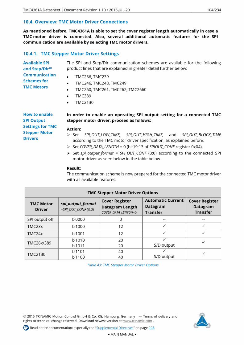
TMC4361A Datasheet | Document Revision 1.10 • 2016-JUL-20 104/234
© 2015 TRINAMIC Motion Control GmbH & Co. KG, Hamburg, Germany — Terms of delivery and
rights to technical change reserved. Download newest version at: www.trinamic.com .
Read entire documentation; especially the “Supplemental Directives” on page 228.
MAIN MANUAL
Overview: TMC Motor Driver Connections
As mentioned before, TMC4361A is able to set the cover register length automatically in case a TMC motor driver is connected. Also, several additional automatic features for the SPI communication are available by selecting TMC motor drivers.
TMC Stepper Motor Driver Settings
The SPI and Step/Dir communication schemes are available for the following
product lines that are explained in greater detail further below:
TMC236, TMC239
TMC246, TMC248, TMC249
TMC260, TMC261, TMC262, TMC2660
TMC389
TMC2130
In order to enable an operating SPI output setting for a connected TMC stepper motor driver, proceed as follows:
Action: Set SPI_OUT_LOW_TIME, SPI_OUT_HIGH_TIME, and SPI_OUT_BLOCK_TIME
according to the TMC motor driver specification, as explained before.
Set COVER_DATA_LENGTH = 0 (bit19:13 of SPIOUT_CONF register 0x04).
Set spi_output_format = SPI_OUT_CONF (3:0) according to the connected SPI
motor driver as seen below in the table below.
Result: The communication scheme is now prepared for the connected TMC motor driver
with all available features.
TMC Stepper Motor Driver Options
TMC Motor Driver
spi_output_format
=SPI_OUT_CONF (3:0)
Cover Register Datagram Length COVER_DATA_LENTGH=0
Automatic Current Datagram Transfer
Cover Register Datagram Transfer
SPI output off b’0000 0 -- --
TMC23x b’1000 12
TMC24x b’1001 12
TMC26x/389 b’1010
b’1011
20
20
S/D output
TMC2130 b’1101
b’1100
40
40
S/D output
Table 43: TMC Stepper Motor Driver Options
Available SPI and Step/Dir™ Communication Schemes for TMC Motors
How to enable SPI Output Settings for TMC Stepper Motor Drivers

TMC4361A Datasheet | Document Revision 1.10 • 2016-JUL-20 105/234
© 2015 TRINAMIC Motion Control GmbH & Co. KG, Hamburg, Germany — Terms of delivery and
rights to technical change reserved. Download newest version at: www.trinamic.com .
Read entire documentation; especially the “Supplemental Directives” on page 228.
MAIN MANUAL
When a TMC motor driver receives a current datagram or a cover datagram that
is transmitted via SPI output of TMC4361A, status data is sent back to the
TMC4361A controller immediately. The response is stored in the COVER_DRV_LOW
0x6E and COVER_DRV_HIGH 0x6F registers, just like all other cover requests.
The type and sequence of the status bits that are sent back are dependent on the
selected motor driver. A detailed list for every motor driver is presented in the
next sections, in which the motor driver communication specifics for every driver
family are explained separately.
The mapping of the available status bits to the TMC4361A STATUS register is
similar for each and every TMC stepper motor driver. The last eight
bits – STATUS (31:24) – are equal to the transferred motor status bits. A detailed
overview is given in the register chapter 17.14. (page 202).
TMC4361A also provides one event at EVENTS (30) that is connected with the
motor driver status bits. Here, any of the motor driver status bits can function as
the base for this event.
In order to activate a motor driver status bit for the motor event EVENTS (30), do as follows:
Action: Selected one or more of the motor driver status for the motor event by
assigning MSTATUS_SELECTION = STEP_CONF (23:16) register 0x0A accordingly.
Result: In case one of the selected motor status bits is activated (Wired-Or), the motor
event switch EVENTS (30) generates an event.
In order to generate an interrupt for this motor event, configure the INTR output
accordingly, as explained in section 5.3. (page 26).
TMC Motor Driver Response Datagram and Status Bits
Events and Interrupts based on Motor Driver Status Bits
TMC4361A Datasheet | Document Revision 1.10 • 2016-JUL-20 106/234
© 2015 TRINAMIC Motion Control GmbH & Co. KG, Hamburg, Germany — Terms of delivery and
rights to technical change reserved. Download newest version at: www.trinamic.com .
Read entire documentation; especially the “Supplemental Directives” on page 228.
MAIN MANUAL
Stall Detection and Stop-on-Stall
TMC stepper motor driver chips with stallGuard and stallGuard2 can detect stall
and overload conditions based on the motor’s back-EMF without the need of a
position sensor. The stall detection status is returned via SPI.
For more information, refer to the AppNote “Parameterization of stallGuard2 &
coolStep” that is available online at www.trinamic.com .
Except for TMC23x and TMC24x, which forward three load detection bits, the
motor stall status is represented by one status bit. TMC4361A is able to stop the
internal ramp as soon as a stall is recognized. Because stall bit activation can occur
unwanted during motion with a low velocity, it is also possible to set up a velocity
threshold for the Stop-on-Stall behavior.
In order to activate a Stop-on-Stall for the internal velocity ramp, do as follows:
Action: Set VSTALL_LIMIT register 0x67 [pps] according to minimum absolute velocity
value for a correct stall recognition.
Set stop_on_stall = 1 (bit26 of REFERENCE_CONF register 0x01).
Set drive_after_stall = 0 (bit27 of REFERENCE_CONF register 0x01).
Result: The internal ramp velocity is set immediately to 0 whenever a stall is detected and
the following is true: |VACTUAL| > VSTALL_LIMIT.
Then, the STOP_ON_STALL event is also generated.
i The status bit stallGuard that is directly mapped from the motor stepper
driver, which is listed in STATUS (24). This flag is always activated as soon as
the motor driver generates the stall guard status bit.
i The ACTIVE_STALL status bit = STATUS (11) is activated as soon as a stall is
detected and |VACTUAL| > VSTALL_LIMIT.
In order to activate the internal velocity ramp AFTER a Stop-on-Stall, do as follows:
Action: Read out the EVENTS register 0x0E to unlock the event STOP_ON_STALL.
Set drive_after_stall = 1 (bit27 of REFERENCE_CONF register 0x01).
Result: The internal ramp velocity is no longer blocked by the Stop-on-Stall event.
i In order to activate the Stop-on-Stall behavior again, reset drive_after_stall
again manually to 0.
stallGuard and stallGuard2 Functionality
Representation of the Motor Stall Status
Internal Velocity Ramp Stop-on-Stall Activation
Internal Velocity Ramp Activation after Stop-on-Stall

TMC4361A Datasheet | Document Revision 1.10 • 2016-JUL-20 107/234
© 2015 TRINAMIC Motion Control GmbH & Co. KG, Hamburg, Germany — Terms of delivery and
rights to technical change reserved. Download newest version at: www.trinamic.com .
Read entire documentation; especially the “Supplemental Directives” on page 228.
MAIN MANUAL
TMC23x, TMC24x Stepper Motor Driver
In this chapter specific information pertaining to the setup of TMC23x and TMC24x is provided.
TMC4361A provides the following features in order to support the TMC23x motor
stepper driver family well:
Automatic Mixed Decay chopper mode
ChopSync
Automatic switchover between microstep and fullstep operation
Controlled PWM signal generation and automatic switchover between SPI
and PWM mode; see section 13.2. (page 138).
In the following section, the features are explained in greater detail.
i For further information, please refer to the manual of the particular stepper
driver motor.
In order to activate the SPI data transfer and SPI feature set for a connected TMC23x stepper motor driver, do as follows:
Action: Set spi_output_format = b’1000 (SPI_OUT_CONF register 0x04).
Set COVER_DATA_LENGTH = 0 (SPI_OUT_CONF register 0x04).
Result: TMC23x is selected as connected stepper motor driver.
In order to activate the SPI data transfer and feature set for a connected TMC24x stepper motor driver, do as follows:
Action: Set spi_output_format = b’1001 (SPI_OUT_CONF register 0x04).
Set COVER_DATA_LENGTH = 0 (SPI_OUT_CONF register 0x04).
Result: TMC24x is selected as connected stepper motor driver.
i In addition to the TMC23x features mentioned above, the TMC24x stepper
driver family provides three stallGuard bits as load measurement indicator.
Therefore, the TMC24x stepper family is supported by the TMC4361A for the
following:
Stall detection and
Stop-on-Stall behavior
Turn to next page for more information.
TMC23x/24x Support
TMC23x Setup
TMC24x Setup
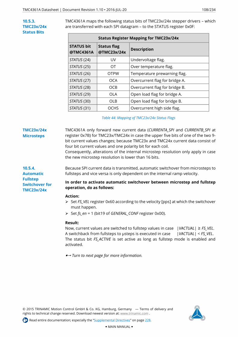
TMC4361A Datasheet | Document Revision 1.10 • 2016-JUL-20 108/234
© 2015 TRINAMIC Motion Control GmbH & Co. KG, Hamburg, Germany — Terms of delivery and
rights to technical change reserved. Download newest version at: www.trinamic.com .
Read entire documentation; especially the “Supplemental Directives” on page 228.
MAIN MANUAL
TMC4361A maps the following status bits of TMC23x/24x stepper drivers – which
are transferred with each SPI datagram – to the STATUS register 0x0F:
TMC4361A only forward new current data (CURRENTA_SPI and CURRENTB_SPI at
register 0x7B) for TMC23x/TMC24x in case the upper five bits of one of the two 9-
bit current values changes; because TMC23x and TMC24x current data consist of
four bit current values and one polarity bit for each coil.
Consequently, alterations of the internal microstep resolution only apply in case
the new microstep resolution is lower than 16 bits.
Because SPI current data is transmitted, automatic switchover from microsteps to
fullsteps and vice versa is only dependent on the internal ramp velocity.
In order to activate automatic switchover between microstep and fullstep operation, do as follows:
Action: Set FS_VEL register 0x60 according to the velocity [pps] at which the switchover
must happen.
Set fs_en = 1 (bit19 of GENERAL_CONF register 0x00).
Result: Now, current values are switched to fullstep values in case |VACTUAL| ≥ FS_VEL.
A switchback from fullsteps to µsteps is executed in case |VACTUAL| < FS_VEL.
The status bit FS_ACTIVE is set active as long as fullstep mode is enabled and
activated.
Turn to next page for more information.
TMC23x/24x Status Bits
Status Register Mapping for TMC23x/24x
STATUS bit @TMC4361A
Status flag @TMC23x/24x
Description
STATUS (24) UV Undervoltage flag.
STATUS (25) OT Over temperature flag.
STATUS (26) OTPW Temperature prewarning flag.
STATUS (27) OCA Overcurrent flag for bridge A.
STATUS (28) OCB Overcurrent flag for bridge B.
STATUS (29) OLA Open load flag for bridge A.
STATUS (30) OLB Open load flag for bridge B.
STATUS (31) OCHS Overcurrent high side flag.
Table 44: Mapping of TMC23x/24x Status Flags
TMC23x/24x Microsteps
Automatic Fullstep Switchover for TMC23x/24x

TMC4361A Datasheet | Document Revision 1.10 • 2016-JUL-20 109/234
© 2015 TRINAMIC Motion Control GmbH & Co. KG, Hamburg, Germany — Terms of delivery and
rights to technical change reserved. Download newest version at: www.trinamic.com .
Read entire documentation; especially the “Supplemental Directives” on page 228.
MAIN MANUAL
TMC4361A supports the mixed decay feature for the TMC23x/24x chopper in
SPI_OUT_CONF register 0x04.
In order to configure mixed decay bits for TMC23x/24x, do as follows:
Action: Set mixed_decay = b’00 if mixed decay must always be deactivated.
Set mixed_decay = b’01 if mixed decay must be activated for each coil during
the falling ramp of the sine curve until reaching value 0.
Set mixed_decay = b’10 if mixed decay must always be activated, except during
standstill.
Set mixed_decay = b’11 if mixed decay must always be activated.
Result: The mixed decay bits for TMC23x/24x stepper motor drivers are set according to
the configuration and the internal MSLUT values.
i Please refer to the TMC23x/TMC24x datasheets to get more information
about the configuration of mixed decay bits.
TMC4361A forwards the internal clock at the output pin STDBY_CLK. This pin can
also be used to provide an external clock for the TMC23x/24x stepper motor
driver. This external clock generator automatically generates clock cycles that are
modified by the chopSync feature if TMC23x/24x is configured as connected
motor driver. Using chopSync enhances the motor drive for fast and smooth
operation.
In order to enable the chopSync clock via the STDBY_CLK pin, do as follows:
Action: Set CHOPSYNC_DIV register 0x1F to generate an external clock frequency fOSC
according to the following equation: fOSC = fCLK / CHOP_SYNC_DIV.
Set stdby_clk_pin_assignment = b’10 (GENERAL_CONF register 0x00).
Result: STDBY_CLK generates an external clock with the selected frequency fOSC that
automatically provides the chopSync feature.
i Recommended minimum external frequency fOSC: two times higher than
audible range.
Because chopper noise is of more concern during standstill than during motion,
TMC4361A provides an option to automatically double the ChopSync frequency
during standby.
If seleceted, a ChopSync frequency within the audible range can be selected. If
doubled, ChopSync frequency operates outside audible range.
In order to enable automatic chopSync frequency doubling, do as follows:
Action: Activate any of the above mentioned mixed_decay options.
Set double_freq_at_stdby = 1 (SPI_OUT_CONF register 0x04).
Result: ChopSync frequency is doubled during standby because CHOPSYNC_DIV is halfed.
Mixed Decay Configuration for TMC23x/24x
ChopSync Configuration for TMC23x/24x Stepper Drivers
Doubling ChopSync Frequency during Standstill

TMC4361A Datasheet | Document Revision 1.10 • 2016-JUL-20 110/234
© 2015 TRINAMIC Motion Control GmbH & Co. KG, Hamburg, Germany — Terms of delivery and
rights to technical change reserved. Download newest version at: www.trinamic.com .
Read entire documentation; especially the “Supplemental Directives” on page 228.
MAIN MANUAL
TMC24x forwards stallGuard values ={LD2&LD1&LD0} instead of one stallGuard2
status bit. These bits represent an unsigned value between 0 and 7. The lower the
value is the higher the mechanical load is. TMC4361A can generate a one-bit
internal stall signal by analyzing the stallGuard values.
In order to set up the stall load limit for automatic stall recognition, do as follows:
Action: Set proper STALL_LOAD_LIMIT (bit10:8 of SPIOUT_CONF register 0x04).
Result: Whenever {LD2&LD1&LD0} ≤ STALL_LOAD_LIMIT a stall is indicated.
This feature also allows use of the Stop-on-Stall feature – already explained in
section 10.4.4, page 106 – because this also applies to other TMC motor stepper
drivers.
Additionally, a standby datagram can be sent automatically when a Stop-on-Stall is executed. In order to activate this behavior, do as follows:
Action: Set VSTALL_LIMIT register 0x67 [pps] according to minimum absolute velocity
value for a correct stall recognition.
Set stop_on_stall = 1 (bit26 of REFERENCE_CONF register 0x01).
Set drive_after_stall = 0 (bit27 of REFERENCE_CONF register 0x01).
Set stdby_on_stall_for_24x = 1 (bit6 of SPIOUT_CONF register 0x04).
Result: Whenever a stall is calculated by comparing STALL_LOAD_LIMIT to the response of
TMC24x, while at the same time the absolute value of VACTUAL exceeds
VSTALL_LIMIT, the internal ramp velocity is stopped immediately. Additionally, both
current values are then set to 0 whereupon a standby mode for the TMC24x
stepper motor driver is generated that switches off all power driver outputs and
clears the error flags.
i To return from Stop-on-Stall, drive_after_stall must be set manually, as stated
further in section 10.4.4 (page 106).
In order to exchange the UV status bit in the STATUS register 0x0F with the calculated stallGuard bit, do as follows:
Action: Set stall_flag_instead_of_uv_en = 1(bit10:8 of SPIOUT_CONF register 0x04).
Result: STATUS (24) shows the calculated stallGuard bit by comparing STALL_LOAD_LIMIT
with the received response datagram of TMC24x.
NOTE:
Please turn page for important NOTICE on connection of STDBY_CLK output pin of
TMC4361A and OSC input pin of TMC23x/24x.
Using TMC24x stallGuard Characteristics

TMC4361A Datasheet | Document Revision 1.10 • 2016-JUL-20 111/234
© 2015 TRINAMIC Motion Control GmbH & Co. KG, Hamburg, Germany — Terms of delivery and
rights to technical change reserved. Download newest version at: www.trinamic.com .
Read entire documentation; especially the “Supplemental Directives” on page 228.
MAIN MANUAL
Connection of STDBY_CLK output pin of TMC4361A and OSC input pin of TMC23x/24x1
Risk of Burns! Avoid overheating and damage of the TMC23x/24x stepper driver and damage of the connected motor!
You MUST use a low pass filter between STDBY_CLK output of TMC4361A and the OSC input pin of TMC23x/24x.
You MUST keep the external clock frequency of the TMC23x/24x stepper motor driver below 50 kHz (to prevent overheating).
This will ensure smooth and safe operation. 1 Per default (i.e. after power on and reset), STDBY_CLK forwards the internal clock that is too high for the TMC23x/24x. See
Figure 10, (page 15) that provides a properly connected sample hardware setup.
NOTICE

TMC4361A Datasheet | Document Revision 1.10 • 2016-JUL-20 112/234
© 2015 TRINAMIC Motion Control GmbH & Co. KG, Hamburg, Germany — Terms of delivery and
rights to technical change reserved. Download newest version at: www.trinamic.com .
Read entire documentation; especially the “Supplemental Directives” on page 228.
MAIN MANUAL
TMC26x Stepper Motor Driver
TMC4361A provides the following features in order to support the TMC26x motor
stepper driver family well:
SPI mode that sets up current values directly.
S/D mode in which the TMC26x processes S/D outputs of TMC4361A.
Automatic switchover between microstep and fullstep operation for both
modes.
Stall detection and Stop-on-Stall behavior for both modes.
S/D mode only: Transfer of automatic scaling values from TMC4361A to
TMC26x.
S/D mode only: Transfer of auto-generated polling datagrams sent by
TMC4361A for reception of status data and microstep position from TMC26x.
In the following section, the features are explained in greater detail.
i For more information, please refer to the manual of the connected stepper
driver motor.
In order to activate the SPI data transfer mode and feature set for a connected TMC26x stepper motor driver, do as follows:
Action: Set spi_output_format = b’1010 (SPI_OUT_CONF register 0x04).
Set COVER_DATA_LENGTH = 0 (SPI_OUT_CONF register 0x04).
Result: TMC26x in SPI mode is selected as connected stepper motor driver. Cover
datagrams and current datagrams are sent via SPI output pins.
In order to activate the S/D mode and feature set for a connected TMC26x stepper motor driver, do as follows:
Action: Connect SPI output pins and S/D outputs to the TMC26x stepper motor driver.
Set spi_output_format = b’1011 (SPI_OUT_CONF register 0x04).
Set COVER_DATA_LENGTH = 0 (SPI_OUT_CONF register 0x04).
Set DIR_SETUP_TIME and STP_LENGTH_ADD (register 0x10) according to the
hardware setup.
Set proper POLL_BLOCK_EXP (bit11:8 of SPIOUT_CONF register 0x04).
Result: TMC26x in S/D mode is selected as connected stepper motor driver. SPI output
pins transfer only cover datagram and automatic configuration datagrams
because motion is generated by processing the STPOUT/DIROUT output signals
of TMC4361A.
The next polling datagram is sent 2^POLL_BLOCK_EXP · SPI_BLOCK_TIME clock cycles
after the last polling datagram.
i A high microstep frequency requires a short SPI datagram polling time.
Continued on next page.
TMC26x Stepper Motor Driver Support
TMC26x Setup (SPI mode)
TMC26x Setup (S/D mode)

TMC4361A Datasheet | Document Revision 1.10 • 2016-JUL-20 113/234
© 2015 TRINAMIC Motion Control GmbH & Co. KG, Hamburg, Germany — Terms of delivery and
rights to technical change reserved. Download newest version at: www.trinamic.com .
Read entire documentation; especially the “Supplemental Directives” on page 228.
MAIN MANUAL
Based on the TMC26x settings - that were explained above - TMC4361A now sends
20-bit datagrams automatically.
In order to send cover datagrams to TMC26x motor stepper drivers, do as follows:
Action: Set COVER_LOW (19:0) to the register values that need to be transferred.
Result: A cover datagram is sent to the connected driver. COVER_DONE is set after data
transfer. The response of TMC26x is stored in COVER_DRV_LOW (19:0).
In case the TMC26x driver operates in SPI mode, COVER_DONE is also set when a
current datagram is transferred.
In order to enable COVER_DONE only for cover datagrams, do as follows:
Action: Set cover_done_only_for_covers = 1 (bit12 of SPI_OUT_CONF register 0x04).
Result: COVER_DONE event is only set if a cover datagram is sent, not for current
datagrams.
It is a common approach that the microcontroller continuously rewrites register
values for TMC26x to respond to possible voltage drops at the VS pin of TMC26x,
which – if they occur – prompt an internal register reset, by design.
TMC4361A provides an option to continuously rewrite the five configuration
registers of TMC26x, which take off workload from the microcontroller.
In order to activate automatic continuous streaming of TMC26x cover datagrams, do as follows:
Action: Set autorepeat_cover_en = 1 (bit7 of SPI_OUT_CONF register 0x04).
Result: In case cover datagrams are sent to TMC26x while autorepeat__cover_en = 1,
TMC4361A transfers a cover datagram every 220 clock cycle. Every time another
register is addressed, the cover datagrams are retransferred one after the other
in consecutive order; i.e. round-robin style.
i However, the transfer rate remains at one datagram per 220 clock cycles.
NOTE:
When TMC26x is operating in SPI mode, current datagrams are also repeated, if
the value does not change; within one transfer interval cycle.
In case a TMC26x register is rewritten manually by cover datagrams, this last
register value is, by definition, repeated.
Automatic register changes executed by TMC4361A – e.g. automatic scaling value
transfers – are considered as well for repeated cover datagrams.
Sending Cover Datagrams to TMC26x
Automatic Continuous Streaming of Cover Datagrams for TMC26x
TMC4361A Datasheet | Document Revision 1.10 • 2016-JUL-20 114/234
© 2015 TRINAMIC Motion Control GmbH & Co. KG, Hamburg, Germany — Terms of delivery and
rights to technical change reserved. Download newest version at: www.trinamic.com .
Read entire documentation; especially the “Supplemental Directives” on page 228.
MAIN MANUAL
Because SPI current data is transmitted, automatic switchover from microsteps to
fullsteps and vice versa entirely depends on internal ramp velocity.
In order to activate automatic switchover between microstep and fullstep operation, do as follows:
Action: Set FS_VEL register 0x60 according to the absolute velocity [pps] at which the
switchover should happen.
Set fs_en = 1 (bit19 of GENERAL_CONF register 0x00).
Result: Now, current values are switched to fullstep values, in case |VACTUAL| ≥ FS_VEL.
A switchback from fullsteps to µsteps is executed, in case |VACTUAL| < FS_VEL.
The status bit FS_ACTIVE is set active as long as fullstep mode is enabled and
activated.
In S/D mode, switchover from microsteps to fullsteps and vice versa is not only
dependent on internal ramp velocity but also on the microstep position of the
TMC26x MSLUT; because switching to a lower resolution must be executed
carefully to catch the correct microstep position. Proper setting of read selection
bits for TMC26x stepper drivers TMC4361A is required to execute switchover
automatically.
In order to activate automatic switchover between microstep and fullstep operation in TMC26x S/D mode, do as follows:
PRECONDITION:
Mandatory TMC26x configuration MUST be executed via cover datagrams: Set RDSEL1 = 0 and RDSEL0 = 0 @TMC26x.
Action: Set disable_polling = 0 (bit6 of SPI_OUT_CONF register 0x04).
Set FS_VEL register 0x60 according to the absolute switching velocity [pps].
Set fs_en = 1 (bit19 of GENERAL_CONF register 0x00).
Set fs_sdout = 0 (bit20 of GENERAL_CONF register 0x00).
Result: The µstep resolution of TMC26x is set to fullsteps, in case |VACTUAL| ≥ FS_VEL.
A switchback from fullsteps to µsteps is executed in case |VACTUAL| < FS_VEL.
FS_ACTIVE is set active as long as fullstep mode is enabled and activated.
Presettings of the TMC26x DRVCTRL register – that is executed beforehand via cover
datagrams – are considered whenever the particular register is overwritten with a
newly assigned microstep resolution.
Turn page for information on changing current scaling parameters for TMC26x in
S/D mode.
TMC26x SPI Mode: Automatic Fullstep Switchover
TMC26x S/D Mode: Automatic Fullstep Switchover

TMC4361A Datasheet | Document Revision 1.10 • 2016-JUL-20 115/234
© 2015 TRINAMIC Motion Control GmbH & Co. KG, Hamburg, Germany — Terms of delivery and
rights to technical change reserved. Download newest version at: www.trinamic.com .
Read entire documentation; especially the “Supplemental Directives” on page 228.
MAIN MANUAL
SPI mode-supported TMC26x drivers are automatically scaled by means of
current datagrams. In order to automatically scale the current of a connected
TMC26x motor stepper driver in S/D mode, TM4361-LA sends auto-generated
cover datagrams by altering directly the CS value of the TMC26x SGCSCONF
register.
TMC4361A provides features that change the current scaling automatically, which
are explained in chapter 11, page 125.
In order to activate automatic current scaling for a connected TMC26x in S/D mode, do as follows:
Action: Set scale_val_transfer_en = 1 (bit5 of SPI_OUT_CONF register 0x04).
Set the scale value register 0x06 and scale configuration register 0x05
according to your requirements (see chapter 11, page 125).
Result: If the current scaling is adapted internally, TMC4361A automatically sends cover
datagrams to TMC26x that change the CS bit directly.
Presettings of the TMC26x SGCSCONF register – that are executed beforehand via
cover datagrams – become considered whenever the particular register is
overwritten with a newly assigned current scaling value.
NOTE:
Please consider that the CS value consists of 5 bits only. Therefore, the scaling
values in register 0x06 must be adapted to 5-bit values as well.
Turn page for information on status transfer of TMC26x.
TMC 26x S/D Mode: Change of Current Scaling Parameter
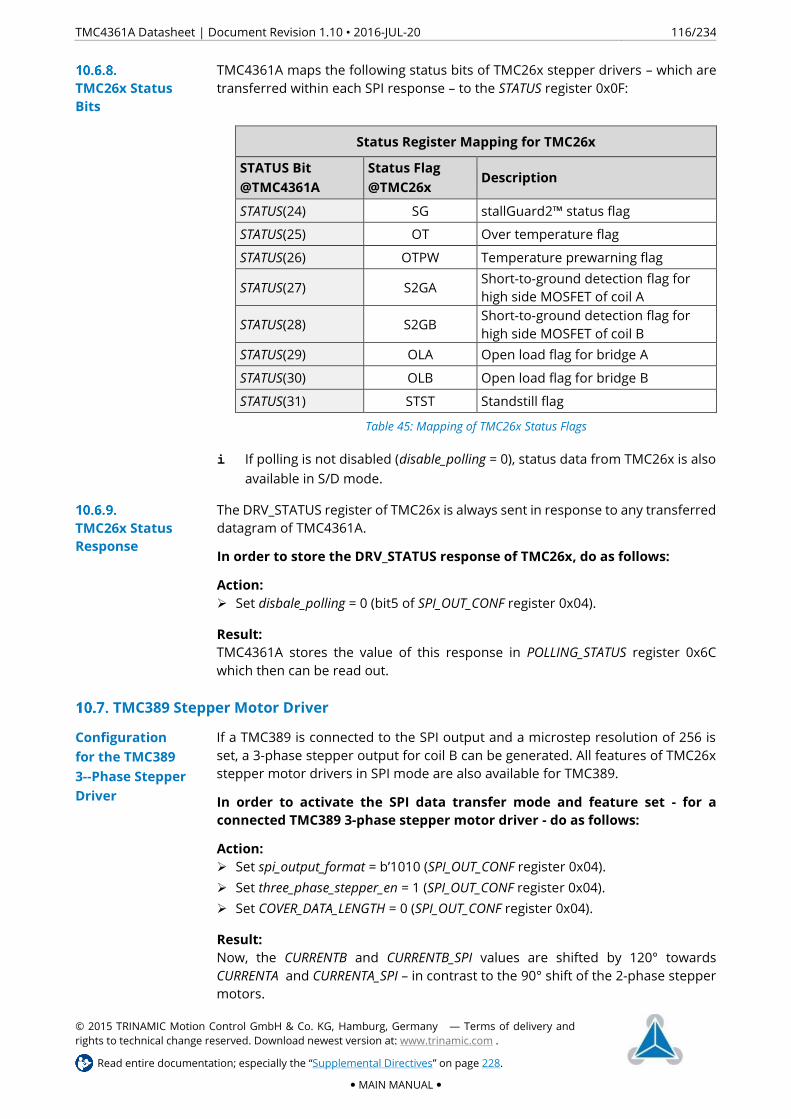
TMC4361A Datasheet | Document Revision 1.10 • 2016-JUL-20 116/234
© 2015 TRINAMIC Motion Control GmbH & Co. KG, Hamburg, Germany — Terms of delivery and
rights to technical change reserved. Download newest version at: www.trinamic.com .
Read entire documentation; especially the “Supplemental Directives” on page 228.
MAIN MANUAL
TMC4361A maps the following status bits of TMC26x stepper drivers – which are
transferred within each SPI response – to the STATUS register 0x0F:
Status Register Mapping for TMC26x
STATUS Bit @TMC4361A
Status Flag @TMC26x
Description
STATUS(24) SG stallGuard2™ status flag
STATUS(25) OT Over temperature flag
STATUS(26) OTPW Temperature prewarning flag
STATUS(27) S2GA Short-to-ground detection flag for
high side MOSFET of coil A
STATUS(28) S2GB Short-to-ground detection flag for
high side MOSFET of coil B
STATUS(29) OLA Open load flag for bridge A
STATUS(30) OLB Open load flag for bridge B
STATUS(31) STST Standstill flag
Table 45: Mapping of TMC26x Status Flags
i If polling is not disabled (disable_polling = 0), status data from TMC26x is also
available in S/D mode.
The DRV_STATUS register of TMC26x is always sent in response to any transferred
datagram of TMC4361A.
In order to store the DRV_STATUS response of TMC26x, do as follows:
Action: Set disbale_polling = 0 (bit5 of SPI_OUT_CONF register 0x04).
Result: TMC4361A stores the value of this response in POLLING_STATUS register 0x6C
which then can be read out.
TMC389 Stepper Motor Driver
If a TMC389 is connected to the SPI output and a microstep resolution of 256 is
set, a 3-phase stepper output for coil B can be generated. All features of TMC26x
stepper motor drivers in SPI mode are also available for TMC389.
In order to activate the SPI data transfer mode and feature set - for a connected TMC389 3-phase stepper motor driver - do as follows:
Action: Set spi_output_format = b’1010 (SPI_OUT_CONF register 0x04).
Set three_phase_stepper_en = 1 (SPI_OUT_CONF register 0x04).
Set COVER_DATA_LENGTH = 0 (SPI_OUT_CONF register 0x04).
Result: Now, the CURRENTB and CURRENTB_SPI values are shifted by 120° towards
CURRENTA and CURRENTA_SPI – in contrast to the 90° shift of the 2-phase stepper
motors.
TMC26x Status Bits
TMC26x Status Response
Configuration for the TMC389 3--Phase Stepper Driver

TMC4361A Datasheet | Document Revision 1.10 • 2016-JUL-20 117/234
© 2015 TRINAMIC Motion Control GmbH & Co. KG, Hamburg, Germany — Terms of delivery and
rights to technical change reserved. Download newest version at: www.trinamic.com .
Read entire documentation; especially the “Supplemental Directives” on page 228.
MAIN MANUAL
TMC2130 Stepper Motor Driver
TMC4361A provides the following features in order to support the TMC2130
motor stepper driver well:
SPI mode that sets up current values directly.
S/D mode in which the TMC2130 processes S/D outputs of TMC4361A.
Automatic switchover between microstep and fullstep operation for both
modes.
Stall detection and Stop-on-Stall behavior for both modes.
S/D mode only: Transfer of automatic scaling datagrams from TMC4361A to
TMC2130.
S/D mode only: Transfer of auto-generated polling datagrams sent by
TMC4361A for reception of status data and microstep position from
TMC2130.
In the following section, the features are explained in greater detail.
i For more information, please refer to the manual of the TMC2130 stepper
driver motor.
In order to activate the SPI data transfer mode and feature set - for a connected TMC2130 stepper motor driver - do as follows:
Action: Set spi_output_format = b’1101 (SPI_OUT_CONF register 0x04).
Set COVER_DATA_LENGTH = 0 (SPI_OUT_CONF register 0x04).
Result: TMC2130 in SPI mode is selected as connected stepper motor driver. Cover
datagrams and current datagrams are sent via SPI output pins.
In order to activate the S/D mode and feature set - for a connected TMC2130 stepper motor driver - do as follows:
Action: Connect SPI output pins and S/D outputs to the TMC2130 stepper motor driver.
Set spi_output_format = b’1100 (SPI_OUT_CONF register 0x04).
Set COVER_DATA_LENGTH = 0 (SPI_OUT_CONF register 0x04).
Set DIR_SETUP_TIME and STP_LENGTH_ADD (register 0x10) according to the
hardware setup.
Set proper POLL_BLOCK_EXP (bit11:8 of SPIOUT_CONF register 0x04).
Result: TMC2130 in S/D mode is selected as connected stepper motor driver. SPI output
pins transfer only cover datagrams and automatic configuration datagrams
because motion is generated by processing the STPOUT/DIROUT output signals
of TMC4361A.
The next polling datagram is sent 2^POLL_BLOCK_EXP · SPI_BLOCK_TIME clock cycles
after the last polling datagram.
i A high microstep frequency requires a short SPI datagram polling time.
TMC2130 Support
Set-up TMC2130 Support (SPI Mode)
Set-up TMC2130 Support (S/D Mode)

TMC4361A Datasheet | Document Revision 1.10 • 2016-JUL-20 118/234
© 2015 TRINAMIC Motion Control GmbH & Co. KG, Hamburg, Germany — Terms of delivery and
rights to technical change reserved. Download newest version at: www.trinamic.com .
Read entire documentation; especially the “Supplemental Directives” on page 228.
MAIN MANUAL
Based upon the TMC2130-supported settings explained above, the TMC4361A
now sends 40 bit datagrams automatically.
In order to send cover datagrams to TMC2130 stepper drivers, do as follows:
Action: Set COVER_HIGH (7:0) register 0x6D to address value that needs to be sent.
Set COVER_LOW (31:0) register 0x6C to data values that needs to be sent.
Result: A cover datagram is sent to the connected driver. COVER_DONE is set after data
transfer. The response of TMC2130 is stored in COVER_DRV_HIGH (7:0) and
COVER_DRV_LOW (31:0).
In case the TMC2130 driver operates in SPI mode, COVER_DONE is also set when a
current datagram is transferred. This also applies to polling datagrams, explained
in section 10.8.8, page 120.
In order to enable COVER_DONE only for cover datagrams, do as follows:
Action: Set cover_done_only_for_covers = 1 (bit12 of SPI_OUT_CONF register 0x04).
Result: COVER_DONE event is only set if a cover datagram is sent, not for current
datagrams.
It is a common approach that the microcontroller continuously rewrites register
values for TMC2130 to respond to possible voltage drops at the VS pin of
TMC2130, which – if they occur – prompt an internal register reset, by design.
TMC4361A provides an option to continuously rewrite five configuration registers
of TMC2130, which take off workload from the microcontroller.
These registers are: GCONF 0x00, IHOLD_IRUN 0x10, CHOPCONF 0x6C, COOLCONF 0x6D, and DCCTRL 0x6E.
In order to activate automatic continuous streaming of TMC2130 cover datagrams, do as follows:
Action: Set autorepeat_cover_en = 1 (bit7 of SPI_OUT_CONF register 0x04).
Result: In case cover datagrams are sent to TMC2130 register – that are mentioned
above – while autorepeat_cover_en = 1, TMC4361A transfers a cover datagram
every 220 clock cycle. Everytime another register is addressed, the cover
datagrams are retransferred one after the other in consecutive order; i.e. round-
robin style.
i However, the transfer rate remains at one datagram per 220 clock cycles.
NOTE:
When TMC2130 is operating in SPI mode, current datagrams are also repeated, if
the value does not change; within one transfer interval cycle.
In case one of the five above mentioned TMC2130 register is rewritten manually by
cover datagrams, this last register value is, by definition, repeated.
Automatic register changes executed by TMC4361A – e.g. automatic scaling value
transfers – are considered as well for repeated cover datagrams.
Sending Cover Datagrams to TMC2130
Automatic Continuous Streaming of Cover Datagrams for TMC2130

TMC4361A Datasheet | Document Revision 1.10 • 2016-JUL-20 119/234
© 2015 TRINAMIC Motion Control GmbH & Co. KG, Hamburg, Germany — Terms of delivery and
rights to technical change reserved. Download newest version at: www.trinamic.com .
Read entire documentation; especially the “Supplemental Directives” on page 228.
MAIN MANUAL
Because SPI current data is transmitted, the automatic switchover from
microsteps to fullsteps and vice versa entirely depends on the internal ramp
velocity.
In order to activate automatic switchover between microstep and fullstep operation, do as follows:
Action: Set FS_VEL register 0x60 according to absolute velocity [pps] at which the
switchover should happen.
Set fs_en = 1 (bit19 of GENERAL_CONF register 0x00).
Result: Now, current values are switched to fullstep values, in case |VACTUAL| ≥ FS_VEL.
A switchback from fullsteps to µsteps is executed in case |VACTUAL| < FS_VEL.
The status bit FS_ACTIVE is set active as long as fullstep mode is enabled and
activated.
During S/D mode, switchover from microsteps to fullsteps and vice versa is only
executed directly by TMC2130. Therefore, a fullstep velocity must only be defined
in TMC2130. TMC4361A transfers microsteps whether TMC2130 is operating in
fullstep or microstep mode.
TMC4361A provides features that change the current scaling automatically, which
is explained in chapter 11, page 125. Stepper motor drivers that are supported by
SPI current datagrams are automatically scaled via current datagrams. To
automatically scale the current of a connected TMC2130 motor stepper driver in
S/D mode, TM4361-LA sends auto-generated cover datagrams by altering the CS
value of the TMC2130 IHOLD_IRUN register.
In order to activate automatic current scaling for TMC2130 in S/D mode:
Action: Set scale_val_transfer_en = 1 (bit5 of SPI_OUT_CONF register 0x04).
Set scale value register 0x06 and scale configuration register 0x05 according
to your requirements (see chapter 11, page 125).
Result: When current scaling is adapted internally, TMC4361A sends cover datagrams to
TMC2130 automatically, which changes the CS bit directly.
Presettings of the IHOLD_IRUN register of the TMC2130 – executed before via
cover datagrams – are considered whenever the particular register is overwritten
with a newly assigned current scaling value.
i Please consider that the IRUN and IHOLD values consist of 5 bits only.
Therefore, scaling values in register 0x06 must also be adapted to 5-bit
values.
TMC2130 SPI Mode: Automatic Fullstep Switchover
TMC2130 S/D Mode: Automatic Fullstep Switchover
TMC 2130 S/D Mode: Changing current Scaling Parameter

TMC4361A Datasheet | Document Revision 1.10 • 2016-JUL-20 120/234
© 2015 TRINAMIC Motion Control GmbH & Co. KG, Hamburg, Germany — Terms of delivery and
rights to technical change reserved. Download newest version at: www.trinamic.com .
Read entire documentation; especially the “Supplemental Directives” on page 228.
MAIN MANUAL
TMC4361A maps the following status bits of TMC2130 stepper drivers – which are
transferred within each SPI response – to the STATUS register 0x0F:
Status Register Mapping for TMC2130
STATUS Bit @TMC4361A Status Flag @TMC2130 Description
STATUS (24) SG stallGuard2™ status flag.
STATUS (25) OT Over temperature flag.
STATUS (26) OTPW Temperature prewarning flag.
STATUS (27) S2GA Short-to-ground detection flag
for high side MOSFET of coil A.
STATUS (28) S2GB Short-to-ground detection flag
for high side MOSFET of coil B.
STATUS (29) OLA Open load flag for bridge A.
STATUS (30) OLB Open load flag for bridge B.
STATUS (31) STST Standstill flag.
Table 46: Mapping of TMC2130 Status Flags
i If polling is not disabled (disable_polling = 0), status data from TMC2130 is also
available in S/D mode.
TMC4361A continuously polls five status registers of TMC2130, if not disabled.
These register are GSTAT 0x01, PWM_SCALE 0x71, LOST_STEPS 0x73 and
DRV_STATUS 0x6F.
In order to store the polled register values of TMC2130, do as follows:
Action: Set disbale_polling = 0 (bit5 of SPI_OUT_CONF register 0x04).
Result: TMC4361A stores the value of DRV_STATUS in POLLING_STATUS register 0x6C,
which then can be read out.
The response for polling of GSTAT, PWM_SCALE and LOST_STEPS are merged in
the POLLING_REG register 0x6D, which then can also be read out.
TMC2130 Status Bits
TMC2130 Status Response

TMC4361A Datasheet | Document Revision 1.10 • 2016-JUL-20 121/234
© 2015 TRINAMIC Motion Control GmbH & Co. KG, Hamburg, Germany — Terms of delivery and
rights to technical change reserved. Download newest version at: www.trinamic.com .
Read entire documentation; especially the “Supplemental Directives” on page 228.
MAIN MANUAL
Connecting Non-TMC Stepper Motor Driver or SPI-DAC at SPI output interface
TMC4361A also provides configuration data for driver chips of other companies via the cover registers. The following output format settings can be selected:
Non-TMC Data Transfer Options
Output Formats spi_output_format Comment
SPI output off b’0000 SPI output driver pins are switched off.
Cover output only b’1111 Only cover datagrams are sent via the SPI output pins.
Unsigned scaling
factor b’0100
The actual unsigned current scaling value is provided at the
SPI output pins.
Signed current data b’0101 Both actual signed current values are provided in one
datagram at the SPI output pins.
DAC scaling factor b’0110 The actual unsigned current scaling value is provided at the
SPI output pins for a defined DAC address.
DAC absolute values b’0011
Both actual signed current values are provided in two
datagrams at the SPI output pins for defined DAC addresses,
which are absolute values.
Phase bits are generated at the STPOUT/DIROUT interface.
Phase bit = 0 signifies positive values.
DAC absolute values b’0010
Both actual signed current values are provided in two
datagrams at the SPI output pins for defined DAC addresses,
which are absolute values.
Phase bits are generated at the STPOUT/DIROUT interface.
Phase bit = 1 signifies positive values.
DAC adapted values b’0001
Both actual signed current values are provided in two
datagrams at the SPI output pins for defined DAC addresses.
These values are mapped to positive values:
Current value equals minimum value (-255) = 0
Current value equals 0 = 128
Current value equals maximum value (+255) = 255
Table 47: Non-TMC Data Transfer Options
NOTE:
Please note that the COVER_DATA_LENGTH must be set according to the predefined driver chip datagram
length.
In order to send cover datagrams only, use this option to avoid datagrams that send scaling or current values whenever these internal values are changed. Please keep in mind that only the SPI protocol is available that is used for
TMC motor stepper drivers.
Setting spi_output_format = b’0100 leads to a transfer of the 8-bit scaling factor if
this value is altered internally: Output data(7:0) = SCALE_PARAM (7:0).
The MSB 7 is sent first. If more than 8 bits are configured as COVER_DATA_LENGTH,
leading zeros are inserted before the MSB.
Setting spi_output_format = b’0101 leads to a transfer of both signed current values
that consists of 18 bits and are sent one after the other in one datagram:
Output data(17:0) = CURRENTA_SPI (8:0) & CURRENTB_SPI (8:0).
The MSB (bit17) is sent first. If more than 18 bits are configured as
COVER_DATA_LENGTH, leading zeros are inserted before the MSB.
Cover Output only !
Sending unsigned Scaling Factor
Sending signed Current Values

TMC4361A Datasheet | Document Revision 1.10 • 2016-JUL-20 122/234
© 2015 TRINAMIC Motion Control GmbH & Co. KG, Hamburg, Germany — Terms of delivery and
rights to technical change reserved. Download newest version at: www.trinamic.com .
Read entire documentation; especially the “Supplemental Directives” on page 228.
MAIN MANUAL
Connecting a SPI-DAC
Connecting a compatible SPI-DAC to SPI output pins, several possibilities are available for output configuration:
Output of the internal SPI current values.
Output of the internal current scaling value.
Several SPI protocols are available.
SPI-DACs can convert more than one digital value, but every value is transmitted
in one datagram. Because TMC4361A provides two current values, a datagram
transfer from TMC4361A to a connected SPI-DAC is split into two datagrams, one
for each current value: CURRENTA_SPI and CURRENTB_SPI.
The transmission is initiated as soon as one of both values is changed internally.
The data transfer of the second current value CURRENTB_SPI is executed
automatically whenever the transmission of CURRENTA_SPI is completed.
If only the scaling factor SCALE_PARAM needs to be transferred, only one datagram
is sent out.
Per default, the SPI protocol follows the TMC style: To initiate a data transfer, the
negated chip select signal NSCSDRV_SDO switches from high to low level. After a
while, the serial clock SCKDRV_NSDO switches from high to low level. When the
transmission is finished, the serial clock switches to high level. Afterwards, the
negated chip select signal switches to high level to finish the data transfer.
Adaptations to suit other SPI protocols are also available:
In order to set serial clock to low level - before the negated chip select switches to low level - do as follows:
Action: Set sck_low_before_csn = 1 (bit4 of SPIOUT_CONF register 0x04).
Result: SCKDRV_NSDO is tied low before NSCSDRV_SDO switches to low level to initiate
data transfer.
Per default, TMC drivers sample master data with the rising edge of the serial
master clock. Thus, TMC4361A shifts output data at SDODRV_SCLK with the falling
edge of SCKDRV_NSDO.
If the data must be sampled with the falling edge of the master clock at the driver’s side, do as follows:
Action: Set new_out_bit_at_rise = 1 (bit5 of SPIOUT_CONF register 0x04).
Result: The output data at SDODRV_SCLK is changed with the rising edge of
SCKDRV_NSDO.
DAC Output Values
DAC Data Transfer
Changing SPI Output Protocol for SPI-DAC

TMC4361A Datasheet | Document Revision 1.10 • 2016-JUL-20 123/234
© 2015 TRINAMIC Motion Control GmbH & Co. KG, Hamburg, Germany — Terms of delivery and
rights to technical change reserved. Download newest version at: www.trinamic.com .
Read entire documentation; especially the “Supplemental Directives” on page 228.
MAIN MANUAL
SPI transmission to a DAC transfers an address or a command prior to the value
that must be defined. The length of the prefixed command/address can be
assigned by setting DAC_CMD_LENGTH according to specification of the SPI-DAC.
In order to set up the DAC communication scheme, do as follows:
Action: Set DAC_CMD_LENGTH (bit11:7 of SPI_OUT_CONF register 0x04) according to the
length of the address / command, which is placed in front of the values.
Set DAC_ADDR register 0x1D according to your requirements:
Address/command of the 1st value: Set DAC_ADDR(15:0) = DAC_ADDR_A.
Address/command of the 2nd value: Set DAC_ADDR(31:16)= DAC_ADDR_B.
Result: DAC_ADDR_A is placed in front of the first transferred value that can be the current
value of coilA (=CURRENTA_SPI) or the scaling factor (=SCALE_PARAM), whereas
DAC_ADDR_B is placed before the second current value CURRENTB_SPI.
i COVER_DATA_LENGTH comprises the whole datagram length, which is the sum
of the address/length DAC_CMD_LENGTH and the 8-bit data length.
i If the cover register length comprises more bits than the combination of
address/command and value, trailing zeros are added at the end.
i The command bits consist of the least significant bits of DAC_ADDR_x if the
command length is less than 16 bits long.
Several opportunities are available for the DAC data style:
Current values are converted to absolute values. The phases of the values are
generated at the STPOUT (coilA) and DIROUT (coilB) pins. The base line (value
equals 0) is located at 0 (see Table 47, Figures B and C).
The current values – which range between -255 and 255 – are mapped to values
between 0 and +255: the minimum value of -255 is an output value of 0, whereas
the baseline is set to +128. The maximum value remains at +255. In detail, the
value is divided by two and 128 is added to the quotient (Table 47, p. 124, Fig. A).
TMC4381 provides an offset to compensate for a shifted DAC baseline.
In order to shift the DAC baseline, do as follows:
Action: Set DAC_OFFSET (bit31:24 of register 0x7E) according to your requirements.
Result: The digital values are shifted accordingly. Table 47 (Page 124), Figure D shows
absolute DAC values. The DAC baseline is shifted by 32 steps, whereas Table 47
(page 124), Figure E shows mapped DAC values, which are shifted by 64 steps.
i For the three available absolute values options – including the unsigned scale
parameter transfer – the offset represents an unsigned number.
i For the mapped values option the offset represents a signed number. To
avoid a carry over at the value limits +255 and -256 when using an DAC offset,
the MSLUT values must be scaled down for the SPI output values
(see Table 47 (page 124), figures D and E). This can be done by using the
current scale feature, as explained in chapter 11, page 125.
Continued on next page.
DAC Address Values
DAC Data Values

TMC4361A Datasheet | Document Revision 1.10 • 2016-JUL-20 124/234
© 2015 TRINAMIC Motion Control GmbH & Co. KG, Hamburg, Germany — Terms of delivery and
rights to technical change reserved. Download newest version at: www.trinamic.com .
Read entire documentation; especially the “Supplemental Directives” on page 228.
MAIN MANUAL
Available DAC Options for the SPI Output Interface
Original SPI Output Curves: A Mapped DAC values:
B Absolute DAC values (positive phase = 0) C Absolute DAC values (positive phase = 1)
D Absolute DAC values, original MSLUT
values are scaled to ½, DAC value offset=32
E Mapped DAC values, original MSLUT values
are scaled to ½, DAC value offset = 64
Table 48: Available SPI-DAC Options
-256
-128
0
128
256
Original SPI output values
CURRENTA_SPI CURRENTB_SPI
0
64
128
192
256
Mapped DAC values
DAC value A DAC value B
0
64
128
192
256
DAC values
DAC value A DAC value B
0
64
128
192
256
DAC values
DAC value A DAC value B
0
1
Phase value coil A
STPOUT
0
1
Phase value coil A
STPOUT
0
1
Phase value coil B
DIROUT
0
1
Phase value coil B
DIROUT
0
64
128
192
256
DAC values
DAC value A DAC value B
0
64
128
192
256
Mapped DAC values
DAC value A DAC value B

TMC4361A Datasheet | Document Revision 1.10 • 2016-JUL-20 125/234
© 2015 TRINAMIC Motion Control GmbH & Co. KG, Hamburg, Germany — Terms of delivery and
rights to technical change reserved. Download newest version at: www.trinamic.com .
Read entire documentation; especially the “Supplemental Directives” on page 228.
MAIN MANUAL
11. Current Scaling
The current values of register 0x7A – CURRENTA and CURRENTB – of the microstep lookup table (MSLUT) represent the maximum 9-bit signed values, which can be sent via the SPIOUT output interface. In most sections of the velocity ramp it is not required to drive the motor with the full current amplitude. Various possibilities are implemented that allow adaptation of actual current values of the MSLUT to the present ramp status. Scale parameters are available for boost current, hold current, and drive current.
These parameters can be assigned independently in the SCALE_VALUES register 0x06, and are used automatically for different states of the velocity ramp; if enabled, as described below. Prior to describing the various feasible scaling situations, a brief explanation of the scaling calculation is provided.
When scaling is enabled for the present ramp state, the actual current values of
the MSLUT are multiplied with the MULT_SCALE parameter that is deduced from
one of the four SCALE_VALUES:
MULT_SCALE = (actual_SCALE_VAL + 1) / 256
with actual_SCALE_VAL = {HOLD, BOOST, DRV1, DRV2}.
Consequently, this MULT_SCALE ranges from 0 to 1: 0 < MULT_SCALE ≤ 1.
MULT_SCALE is then multiplied with the actual current values CURRENTA and
CURRENTB, which are generated by the MSLUT:
CURRENTA_SPI = CURRENTA · MULT_SCALE (bit8:0 of 0x7B)
CURRENTB_SPI = CURRENTB · MULT_SCALE (bit24:16 of 0x7B)
These values are transferred via SPI output interface. If no current scaling is
enabled, the output values CURRENTA_SPI and CURRENTB_SPI are equal to the
MSLUT values CURRENTA and CURRENTB because the scaling values are equal to
the maximum 255, per default. Thus, scaling will only decrease the original MSLUT
values.
Also, the actual scale parameter can assume intermediate values because
TMC4361A offers possibilities to convert smoothly from one scale value to
another. The actual scale parameter SCALE_PARAM can be read out at register
0x7C. It has the same range as the four SCALE_VALUES.
Use of TMC26x and TMC2130 stepper motor drivers in S/D mode: If TMC motor stepper drivers are used in S/D mode, scaling values comprise only
5 bits because the CS value of TMC26x, and the IHOLD, IRUN values of TMC2130
motor stepper drivers are adapted directly. Therefore, MULT_SCALE is calculated
slightly differently:
MULT_SCALE = (actual_SCALE_VAL + 1) / 32
Calculation of the Current Output Values
Description of
Scaling
Calculation
AREAS OF SPECIAL CONCERN
!

TMC4361A Datasheet | Document Revision 1.10 • 2016-JUL-20 126/234
© 2015 TRINAMIC Motion Control GmbH & Co. KG, Hamburg, Germany — Terms of delivery and
rights to technical change reserved. Download newest version at: www.trinamic.com .
Read entire documentation; especially the “Supplemental Directives” on page 228.
MAIN MANUAL
During standstill, the current can be scaled down considerably in most
applications because the energy demand is lower than during motion. In addition
to the scaling value, the standby delay must be configured. The delay defines the
time between ramp stop and startup of hold scaling. Whenever the delay is set
to 0, hold scaling is immediately enabled at the end of the velocity ramp. Because
most applications require waiting for system oscillations after ramp stop, this
delay must be set up in most cases.
In order to set up and enable hold current scaling, do as follows:
Action: Set the time frame for STDBY_DEALY register 0x15 after ramp stop, and before
standby phase starts.
Set HOLD_SCALE_VAL = SCALE_VALUES (31:24) according to the maximum current
during motor standstill.
Set hold_current_scale_en = 1 (CURRENT_CONF register 0x05).
Set closed_loop_scale_en = 0 (CURRENT_CONF register 0x05).
Result: The standby timer is started as soon as VACTUAL reaches 0. After STDBY_DELAY
clock cycles the standby timer expires that activates the hold scaling phase.
The standby status can be forwarded via STDBY_CLK output pin.
In order to generate an output standby signal, do as follows:
Action: Set stdby_clk_pin_assignment (1) = 0 (Bit14 of GENERAL_CONF register 0x00).
Set stdby_clk_pin_assignment (0) (Bit13 of GENERAL_CONF register 0x00)
according to the active voltage level of the output pin.
Result: STDBY_CLK output pin forwards the internally generated standby status. The
active output level equals stdby_clk_pin_assignment (0).
Some applications require a freewheeling behavior after ramp stop. This means
that the current values are set to 0. A delay timer can be configured to define the
time between standby start and the beginning of freewheeling.
In order to set up and enable freewheeling, do as follows:
Action: Set FREEWHEEL_DELAY register 0x16 according to the duration of the time after
standby start, so that freewheeling is activated accordingly.
Set freewheeling_en = 1 (CURRENT_CONF register 0x05).
Set closed_loop_scale_en = 0 (CURRENT_CONF register 0x05).
Result: The freewheeling timer is started as soon as the standby mode is activated. After
completion of FREEWHEEL_DELAY clock cycles, the freewheeling timer expires that
activates the freewheeling phase.
i Just before the velocity ramps starts internal scaling is set to the standby
scaling value. This avoids starting the ramp at current values that are equal
to 0.
Hold Current Scaling
Standby Status
Freewheeling

TMC4361A Datasheet | Document Revision 1.10 • 2016-JUL-20 127/234
© 2015 TRINAMIC Motion Control GmbH & Co. KG, Hamburg, Germany — Terms of delivery and
rights to technical change reserved. Download newest version at: www.trinamic.com .
Read entire documentation; especially the “Supplemental Directives” on page 228.
MAIN MANUAL
Current Scaling during Motion
If the current values need to be scaled during motion, several options are available. Up to three scaling values can be selected: Two drive scaling values and one boost scale value. Different scale values can be automatically assigned to the various sections of the velocity ramp.
Drive scaling is the preferred direct and mostly unconditional scaling option. If
no boost scaling is enabled, the current values are scaled according to the given
scale value, independent of the present ramp status.
In order to set up and enable only drive current scaling, do as follows:
Action: Set DRV1_SCALE_VAL = SCALE_VALUES (15:8) according to the maximum current
during motion.
Set drive_current_scale_en = 1 (CURRENT_CONF register 0x05).
Set closed_loop_scale_en = 0 (CURRENT_CONF register 0x05).
Result: As long as no other motion scale options are activated the current values of the
MSLUT are scaled according to DRV1_SCALE_VAL during motion (VACTUAL <> 0).
A second drive scale parameter can be assigned in order to differentiate the
motion scaling according to the internal ramp velocity.
In order to set up and enable drive current scaling with two different scaling values, do as follows:
Action: Set VDRV_SCALE_LIMIT register 0x17 [pps] according to switching velocity at
which drive scaling will change.
Set DRV1_SCALE_VAL = SCALE_VALUES(15:8) according to maximum current
during motion below VDRV_SCALE_LIMIT.
Set DRV2_SCALE_VAL = SCALE_VALUES(23:16) according to maximum current
during motion beyond VDRV_SCALE_LIMIT.
Set drive_current_scale_en = 1 (CURRENT_CONF register 0x05).
Set sec_drive_current_scale_en = 1 (CURRENT_CONF register 0x05).
Set closed_loop_scale_en = 0 (CURRENT_CONF register 0x05).
Result: As long as no boost scaling is activated, the current values of the MSLUT are scaled
according to DRV1_SCALE_VAL as long as VACTUAL ≤ VDRV_SCALE_LIMIT.
Whenever VACTUAL > VDRV_SCALE_LIMIT the current values are scaled according
to DRV2_SCALE_VAL.
Drive Scaling
Alternative Drive Scaling

TMC4361A Datasheet | Document Revision 1.10 • 2016-JUL-20 128/234
© 2015 TRINAMIC Motion Control GmbH & Co. KG, Hamburg, Germany — Terms of delivery and
rights to technical change reserved. Download newest version at: www.trinamic.com .
Read entire documentation; especially the “Supplemental Directives” on page 228.
MAIN MANUAL
In certain sections of the velocity ramp it can be useful to boost the current. Boost
current can be assigned temporarily either after ramp start or during the whole
ac-/deceleration phase. All options can be selected separately, or in combination.
i All three options use the same scaling value BOOST_SCALE_VAL.
OPTION 1: BOOST SCALING AT RAMP START
In order to set up and enable boost current scaling within a defined time frame directly after the velocity ramp start-up, do as follows:
Action: Set BOOST_TIME register 0x18 according to the delay period at which boost
current scaling is activated after a velocity ramp start.
Set BOOST_SCALE_VAL = SCALE_VALUES (7:0) according to the maximum current
during the boost phase.
Set boost_current_after_start_en = 1 (CURRENT_CONF register 0x05).
Set closed_loop_scale_en = 0 (CURRENT_CONF register 0x05).
Result: After the velocity ramp start (VACTUAL = 0 before), boost scaling is activated
according to BOOST_SCALE_VAL. The boost timer expires after BOOST_TIME clock
cycles. Afterwards, any other selected scaling value is used, if active and selected.
OPTION 2: BOOST SCALING ON ACCELERATION SLOPES
In order to set up and enable boost current scaling for the acceleration phase of the velocity ramp, do as follows:
Action: Set BOOST_SCALE_VAL = SCALE_VALUES (7:0) according to the maximum current
during the boost phase.
Set boost_current_on_acc_en = 1 (CURRENT_CONF register 0x05).
Set closed_loop_scale_en = 0 (CURRENT_CONF register 0x05).
Result: As long as the absolute internal velocity |VACTUAL| increases, the boost scaling
function is activated according to BOOST_SCALE_VAL. The present ramp state can
be read out by the RAMP_STATE flag. Acceleration slopes are indicated by
RAMP_STATE = b’01.
OPTION 3: BOOST SCALING ON DECELERATION SLOPES
In order to set up and enable boost current scaling for the deceleration phase of the velocity ramp, do as follows:
Action: Set BOOST_SCALE_VAL = SCALE_VALUES(7:0) according to maximum current
during the boost phase.
Set boost_current_on_dec_en = 1 (CURRENT_CONF register 0x05).
Set closed_loop_scale_en = 0 (CURRENT_CONF register 0x05).
Result: As long as the absolute internal velocity |VACTUAL| decreases, boost scaling is
activated according to BOOST_SCALE_VAL. The present ramp state can be read out
at the RAMP_STATE flag. Deceleration slopes are indicated by RAMP_STATE = b’10.
Boost Current

TMC4361A Datasheet | Document Revision 1.10 • 2016-JUL-20 129/234
© 2015 TRINAMIC Motion Control GmbH & Co. KG, Hamburg, Germany — Terms of delivery and
rights to technical change reserved. Download newest version at: www.trinamic.com .
Read entire documentation; especially the “Supplemental Directives” on page 228.
MAIN MANUAL
Scale Mode Transition Process Control
Transition from one scale value to the next active value can be configured as slight conversion. It is advisable to avoid abrupt scaling alterations, which can cause unwanted oscillations and/or motor stall. Three different parameters can be set to convert to higher or lower current scale values.
It is often required to peter out the motion (by smoothening the transition process from motion scaling to hold scaling) in order to avoid system standstill oscillations.
In order to configure a smooth transition from motion current scaling to hold current scaling, do as follows:
Action: Set HOLD_SCALE_DELAY register 0x19 according to the delay period after which
the actual scale parameter is decreased by one step towards hold current scale
value.
Result: Immediately after the hold scaling current is activated, the actual scale parameter
is decreased by one step per HOLD_SCALE_DELAY clock cycles until
SCALE_PARAM = HOLD_SCALE_VAL.
i If HOLD_SCALE_DELAY = 0, the hold current scaling value HOLD_SCALE_VAL is
assigned immediately whenever the hold current scaling is activated.
To avoid step loss – in case a higher scale value is assigned during motion – the transition from low to high current scale values can also be adapted.
In order to configure a smooth transition from a lower motion current scaling value to a higher motion current scaling value, do as follows:
Action: Set UP_SCALE_DELAY register 0x18 according to the delay period after which the
actual scale parameter is increased by one step towards the higher current
scale value.
Result: Whenever a higher current scale value is assigned internally, the actual scale
parameter is increased by one step per UP_SCALE_DELAY clock cycles until the
assigned scale parameter is reached.
i If UP_SCALE_DELAY = 0, the higher current scaling value is assigned
immediately whenever the corresponding current scaling phase is activated.
Description continued on next page.
Transition to Hold Current Scaling
!
Transition to higher Motion Current Scaling
!

TMC4361A Datasheet | Document Revision 1.10 • 2016-JUL-20 130/234
© 2015 TRINAMIC Motion Control GmbH & Co. KG, Hamburg, Germany — Terms of delivery and
rights to technical change reserved. Download newest version at: www.trinamic.com .
Read entire documentation; especially the “Supplemental Directives” on page 228.
MAIN MANUAL
To avoid step loss or unwanted oscillations – in case a lower scale value is assigned during motion – the transition from high to low current scale values can be adapted also.
In order to configure a smooth transition from a higher motion current scaling value to a lower motion current scaling value, do as follows:
Action: Set DRIVE_SCALE_DELAY register 0x1A according to the delay period after which
the actual scale parameter is decreased by one step towards the lower current
scale value.
Result: Whenever a lower current scale value is assigned internally, the actual scale
parameter is decreased by one step per DRIVE_SCALE_DELAY clock cycles until the
assigned scale parameter is reached.
i If DRIVE_SCALE_DELAY = 0, the lower current scaling value is assigned
immediately whenever the corresponding current scaling phase is activated.
Two examples are provided on the following pages that illustrate how scaling modes can be used. The scale parameter SCALE_PARAM is shown in combination with its related scale
timers in clock cycles and in combination with the underlying velocity ramp.
Transition to lower Motion Current Scaling
!

TMC4361A Datasheet | Document Revision 1.10 • 2016-JUL-20 131/234
© 2015 TRINAMIC Motion Control GmbH & Co. KG, Hamburg, Germany — Terms of delivery and
rights to technical change reserved. Download newest version at: www.trinamic.com .
Read entire documentation; especially the “Supplemental Directives” on page 228.
MAIN MANUAL
Current Scaling Examples
In this example, the following scale options are enabled:
Standby scaling
Freewheeling
Boost scaling at start
Boost scaling on deceleration ramps
Drive scaling
The different scaling stages of the trapezoidal velocity ramp are shown in different
colors in the Figure A below.
Figure B shows the internal scale parameter SCALE_PARAM as function of time.
The scale parameter is not switched immediately whenever the scaling situations
alters; because delay timers are used. A transition time between the assigned
values is generated. Four transition phases are shown that are calculated as
follows:
tSTART_SCALE = (BOOST_SCALE_VAL – HOLD_SCALE_VAL) · UP_SCALE_DELAY · fCLK
tDN_SCALE = (BOOST_SCALE_VAL – DRV1_SCALE_VAL) · DRV_SCALE_DELAY · fCLK
tUP_SCALE = (BOOST_SCALE_VAL – DRV1_SCALE_VAL) · UP_SCALE_DELAY · fCLK
tHOLD_SCALE = (DRV1_SCALE_VAL – HOLD_SCALE_VAL) · HOLD_SCALE_DELAY · fCLK
Figure C shows the different timers that are used:
To finish boost scaling after start.
To start standby scaling.
To start freewheeling.
i These three delay values are directly determined by their respective register
values 0x1B, 0x15, and 0x16.
Figure 55: Scaling Example 1
v(t)
t
t
SCALE_PARAM
Boost scaling
Drv1 scaling
StdBy scaling
Freewheeling
t
scale timer [clk cycles]
BOOST_SCALE_VAL
DRV1_SCALE_VAL
HOLD_SCALE_VAL
STDBY_DELAY
FREEWHEEL_DELAY
BOOST_TIME
tDN_SCALE tUP_SCALE tDN_SCALE
tHOLD_SCALE
tSTART_SCALE
A)
B)
C)
Scaling Mode Example 1

TMC4361A Datasheet | Document Revision 1.10 • 2016-JUL-20 132/234
© 2015 TRINAMIC Motion Control GmbH & Co. KG, Hamburg, Germany — Terms of delivery and
rights to technical change reserved. Download newest version at: www.trinamic.com .
Read entire documentation; especially the “Supplemental Directives” on page 228.
MAIN MANUAL
In this example, the following scale options are enabled:
Boost scaling on acceleration ramps
Drive scaling 1 and 2
As long as |VACTUAL| < VDRV_SCALE_LIMIT, Drv1 scaling is active. Both drive scaling
modes are used for the deceleration ramp because boost current is not enabled
during deceleration slopes (boost_current_on_dec = 0).
Whenever VACTUAL traverses 0 the RAMP_STATUS switches to acceleration ramp,
and boost scaling becomes enabled again.
This is shown in Figure 53 A. Figure 53 B depicts the actual scale parameter, which
is altered with the formerly specified delays. In contrast to example 1, tSTART_SCALE
is changed to the following calculation:
tDN_SCALE = (BOOST_SCALE_VAL – DRV1_SCALE_VAL) · DRV_SCALE_DELAY · fCLK
Whereas the other transition phases depend on whether DRV1_SCALE_VAL or
DRV2_SCALE_VAL is used either; before or after the transition process.
Figure 56: Scaling Example 2
Scaling Mode Example 2
v(t)
t
t
SCALE_PARAM
VDRV_SCALE_LIMIT
-VDRV_SCALE_LIMIT
Boost scaling
Drv1 scaling
Drv2 scaling
BOOST_SCALE_VAL
DRV1_SCALE_VAL
DRV2_SCALE_VAL

TMC4361A Datasheet | Document Revision 1.10 • 2016-JUL-20 133/234
© 2015 TRINAMIC Motion Control GmbH & Co. KG, Hamburg, Germany — Terms of delivery and
rights to technical change reserved. Download newest version at: www.trinamic.com .
Read entire documentation; especially the “Supplemental Directives” on page 228.
MAIN MANUAL
12. NFREEZE and Emergency Stop
In case dysfunctions at board level occur, some applications require an additional strategy to end current operations without any delay. Therefore, TMC4361A provides the low active safety pin NFREEZE.
NFREEZE is low active. An active NFREEZE input transition from high to low level
stops the current ramp immediately in a user configured way.
At the moment - when NFREEZE switches to low - an event FROZEN is triggered at
EVENTS (10). FROZEN remains active until the reset of the TMC4361A.
It is necessary to tie NFREEZE low for at least three clock cycles because of the input filter of three consecutive sample points.
Pin Description: NFREEZE
Pin Name Type Remarks
NFREEZE Input External enable pin; low active.
Table 49: Pin Description: NFREEZE
Pin Descriptions: DFREEZE and IFREEZE
Register Name Register Address Remarks
DFREEZE 0x4E (23:0) RW Deceleration value in the case of an active FREEZE event.
IFREEZE 0x4E (31:24) RW Current scaling value in the case of an active FREEZE event.
Table 50: Pin Descriptions DFREEZE and IFREEZE
Two parameters (DFREEZE and IFREEZE) are necessary in order to be able to use
the TMC4361A freeze function. They are integrated in the freeze register, which
can be written only once after an active reset; assuming that there has not been
a ramp start before. Thus, the freeze parameters should be set directly before
operation.
NOTE:
Selected values cannot be altered until the next active reset. These restrictions are
necessary to protect the TMC4361A freeze configuration from incorrect SPI data
sent from the microcontroller in case of error.
Keep in mind that:
The polarity of NFREEZE input cannot be assigned.
The freeze register can always be read out.
During freeze state ramp register values can be read out.
NFREEZE Operational Principle
AREAS OF SPECIAL CONCERN
!
Configuration of FREEZE Function
AREAS OF SPECIAL CONCERN
!

TMC4361A Datasheet | Document Revision 1.10 • 2016-JUL-20 134/234
© 2015 TRINAMIC Motion Control GmbH & Co. KG, Hamburg, Germany — Terms of delivery and
rights to technical change reserved. Download newest version at: www.trinamic.com .
Read entire documentation; especially the “Supplemental Directives” on page 228.
MAIN MANUAL
DFREEZE can be used for an automatic ramp stop configuration. Two options are available:
Option 1: Use of DFREEZE = 0 for a hard stop.
Option 2: Use of DFREEZE ≠ 0 for a linear deceleration ramp.
PRINCIPLE:
Due to the independence of DFREEZE from internal register values like
direct_acc_val_en or the given clock frequency fCLK (which can be altered by
erroneous SPI signals) the deceleration value DFREEZE is always given as velocity
value change per clock cycle. Therefore, the DFREEZE value is calculated as follows:
d_freeze [pps²] = DFREEZE / 237 · fCLK2
This leads to the same behavior of the motor and is like setting direct_acc_val_en
to 1 for the other acceleration values during normal operation.
IFREEZE can be used to configure the current scaling value during a freeze event. Two options are available:
Option 1: Use of IFREEZE = 0 for assigning the last specified current scaling
value before the freeze event.
Option 2: Use of IFREEZE ≠ 0 for assigning a defined current scaling value.
PRINCIPLE:
IFREEZE is a current scaling value which becomes valid in case NFREEZE has been
tied to low and the related event (FROZEN) has been released.
In case IFREEZE is set to 0, the last scaling value before the emergency event is
assigned permanently.
The scale value IFREEZE then manipulates the current value in the same way as
explained in chapter 11, page 125.
Configuration of DFREEZE for automatic Ramp Stop
Configuration of IFREEZE current Scaling Value

TMC4361A Datasheet | Document Revision 1.10 • 2016-JUL-20 135/234
© 2015 TRINAMIC Motion Control GmbH & Co. KG, Hamburg, Germany — Terms of delivery and
rights to technical change reserved. Download newest version at: www.trinamic.com .
Read entire documentation; especially the “Supplemental Directives” on page 228.
MAIN MANUAL
13. Controlled PWM Output
TMC4361A offers controlled PWM (Pulse Width Modulation) signals at STPOUT and DIROUT output pins. These PWM signals can be scaled, depending on the internal velocity. If a TMC23x/24x stepper motor driver is connected and configured properly, the PWM signals are redirected to two SPI output interface pins. This avoids rerouting of signal lines at board level if SPI mode is switched to PWM mode, or vice versa.
In this chapter information is provided on the basic setup of the PWM output configuration; and also on TMC23x/24x control PWM input support.
Dedicated PWM Output Pins
Pin Names Type Remarks
STPOUT_PWMA Output PWM output for coil A.
DIROUT_PWMB Output PWM output for coil B.
Connected and selected TMC23x/24x stepper motor drivers only:
SDODRV Output PWM output for coil A.
NSCSDRV Output PWM output for coil B.
Table 51: Dedicated PWM Output Pins
Dedicated PWM Output Registers
Register Name Register Address Remarks
GENERAL_CONF 0x00 RW Bit 21: pwm_out_en.
CURENT_CONF 0x05 RW
pwm_scale_en = CURRENT_CONF (8): PWM scale enable
switch
PWM_AMPL = CURRENT_CONF (31:16): PWM amplitude
at VACTUAL = 0.
PWM_VMAX 0x17 RW
Second assignment to VDRV_SCALE_LIMIT: velocity at
which the PWM scale parameter reaches 1
(maximum).
PWM_FREQ 0x1F RW Number of clock cycles that forms one PWM period.
Table 52: Dedicated PWM Output Registers

TMC4361A Datasheet | Document Revision 1.10 • 2016-JUL-20 136/234
© 2015 TRINAMIC Motion Control GmbH & Co. KG, Hamburg, Germany — Terms of delivery and
rights to technical change reserved. Download newest version at: www.trinamic.com .
Read entire documentation; especially the “Supplemental Directives” on page 228.
MAIN MANUAL
PWM Output Generation and Scaling Possibilities
The STPOUT and DIROUT output pins generally forward internal generated
microsteps and motion direction. In contrast to that, it is possible to forward the
internal MSLUT value as PWM output signals, which is dependent on the PWM
frequency.
In order to generate PWM output, do as follows:
Action: Set PWM_FREQ register 0x1F to the number of clock cycles for one PWM cycle.
Set pwm_out_en = 1 (GENERAL_CONF register 0x00).
Result: Step/Dir output is disabled and PWM signals are forwarded via STPOUT_PWMA
and DIROUT_PWMB. PWM frequency fPWM is calculated by:
fPWM = fCLK / PWM_FREQ
If PWM Voltage mode is selected:
Avoid unintended overheating to prevent motor damage during PWM mode!
At lower velocity values PWM voltage scaling MUST be enabled.
This will ensure smooth operation during controlled PWM mode.
The duty cycle of both signals represent the sine (STPOUT) and cosine (DIROUT)
values of the MSLUT.
PWM voltage scaling does not work the same way as presented for the SPI current
output interface (see chapter 11, page 125). PWM scaling is adapted linearly,
which depends on the internal ramp velocity. During Voltage PWM mode the
scaling value at VACTUAL = 0 must be assigned, and also the velocity at which full
scaling is reached.
In order to generate a scaled PWM output, do as follows:
Action: Set PWM_AMPL (bit31:16 of register 0x05) as start PWM scaling value.
Set PWM_VMAX register 0x17 to the internal ramp velocity [pps] at which full
PWM scaling is reached.
Set pwm_scale = 1 (bit8 of CURRENT_CONF register 0x05).
Result: PWM_SCALE is the actual scaling value.
In case VACTUAL = 0, PWM_SCALE = (PWM_AMPL + 1) / 217.
i Whenever the absolute velocity value increases, the scale parameter also
increases linearly until it reaches the maximum of PWM_SCALE = 0.5 at
VACTUAL = PWM_VMAX.
i The minimum duty cycle is calculated by DUTY_MIN = (0.5 – PWM_SCALE).
i The maximum duty cycle is calculated by DUTY_MAX = (0.5 + PWM_SCALE).
i These values set the PWM duty cycle limits of any internal ramp velocity.
Enable PWM Output Generation
NOTICE
PWM Duty Cycle Scaling

TMC4361A Datasheet | Document Revision 1.10 • 2016-JUL-20 137/234
© 2015 TRINAMIC Motion Control GmbH & Co. KG, Hamburg, Germany — Terms of delivery and
rights to technical change reserved. Download newest version at: www.trinamic.com .
Read entire documentation; especially the “Supplemental Directives” on page 228.
MAIN MANUAL
In Figure 54 below, the calculation of minimum/maximum PWM duty cycles with
PWM_AMPL = 32767 is shown on the left side. Resulting duty cycles for different
positions in the sine voltage curve are depicted on the right side. Calculated delays
of minimum/maximum duty cycles are also shown.
Figure 57: Calculation of PWM Duty Cycles (PWM_AMPL)
NOTE:
If hold current scaling is enabled, see section 11.1. , page 126, HOLD_SCALE_VAL is
used for PWM scaling during standstill.
PWM Scale Example
PWM_SCALE
VACTUALPWM_VMAX
(PWM_AMPL+1)
2^17
0.5
tDUTY_CYCLE
PWM_VMAX
PWM_FREQ
fCLK
tDUTY_MAX=(0.5+PWM_SCALE)•PWM_FREQ/fCLK
tDUTY_MIN=(0.5–PWM_SCALE)•PWM_FREQ/fCLK
VACTUAL
t
voltage(V)
t
t0.5•PWM_FREQ
fCLK
t
I
I I
I I II
I I
I I I

TMC4361A Datasheet | Document Revision 1.10 • 2016-JUL-20 138/234
© 2015 TRINAMIC Motion Control GmbH & Co. KG, Hamburg, Germany — Terms of delivery and
rights to technical change reserved. Download newest version at: www.trinamic.com .
Read entire documentation; especially the “Supplemental Directives” on page 228.
MAIN MANUAL
PWM Output Generation for TMC23x/24x
PWM output signals can be used for TMC23x/24x stepper motor drivers Voltage
PWM mode. TMC4361A forwards the internal PWM output signals at the
corresponding SPI output interface pins because the drivers share input and
output pins for the SPI mode and the Voltage PWM mode. This feature enables
variable operation of the TMC23x/24x in the one or the other mode without
rerouting the particular signal lines at board level.
In order to generate a PWM output for TMC23x/24x stepper motor drivers, do as follows:
Action: Set PWM_FREQ register 0x1F to the number of clock cycles for one PWM cycle.
Set spi_output_format = b’1000 (TMC23x) or
spi_output_format = b’1001 (TMC24x).
Set pwm_out_en = 1 (GENERAL_CONF register 0x00).
Set SPI_SWITCH_VEL register 0x1D to 0.
Result: SPI output interface is disabled, controlled PWM output for TMC23x/24x is
enabled.
SDODRV_SCLK output pin forwards PWM PHA signal.
NSCSDRV_SDO output pin forwards PWM PHB signal.
MP2 is set to low voltage level that disables TMC23x/24x SPI mode.
SDODRV_SCLK analyses the error flags that are forward via SDO output pin
of TMC23x/24x. These error flags indicate overcurrent on any bridge or the
overtemperature flag. Therefore, these three status bits of TMC4361A are
altered according to the ERR flag.
SCKDRV_NSDO is set to high voltage level to set MDBN of TMC23x/24x to
high voltage level.
NOTE:
Only the five pins mentioned above are set accordingly by TMC4361A.
Please be aware that all other pins of TMC23x/24x must be set according to your
requirements, especially ANN/MDAN = high voltage level, and INA resp. INB
according to the current limit.
i For correct hardware setup information refer to TMC23x/24x manuals.
Figure 58: TMC4361A connected with TMC23x/24x operating in SPI Mode or PWM Mode
Controlled PWM Signals for TMC23x/24x
TMC4361A with TMC23x/24x Stepper Driver
TMC4361µC SCK
MOSI
MISO
SS
SCKIN
SDOIN
CLKCLK_EX
T
NSCSIN
SDIIN
SDO/ERR
CSN/PHB
SDI/PHA
SCK/MDBN
TMC23x/24x
M
NSCSDRV_SDO
SDODRV_SCLK
SCKDRV_NSDO
SDIDRV_NSCLK
STDBY_CLK Output for chopSync
OSC
15K
680pF
SPEMP2
ANN/MDAN
VCCIO

TMC4361A Datasheet | Document Revision 1.10 • 2016-JUL-20 139/234
© 2015 TRINAMIC Motion Control GmbH & Co. KG, Hamburg, Germany — Terms of delivery and
rights to technical change reserved. Download newest version at: www.trinamic.com .
Read entire documentation; especially the “Supplemental Directives” on page 228.
MAIN MANUAL
The hardware setup scenario, as shown on the previous page, also allows
switching between SPI and Voltage PWM mode. It is advisable to enable or disable
the Voltage PWM mode during standstill of the internal ramp.
In order to disable Voltage PWM mode for TMC23x/24x, do as follows:
Action: Set pwm_out_en = 0 (GENERAL_CONF register 0x00).
Result: SPI output interface is enabled and controlled PWM output for TMC23x/24x is
disabled. MP2 – that must be connected with SPE@TMC23x/24x – is set to high
voltage level, which enables TMC23x/24x SPI mode.
However, it is also possible to switch between both modes during motion.
Because the internal MSLUT is used either as voltage specification or as current
specification, microstep loss can occur whenever the mode is switched in case the
switching velocity is passed by.
i In order to overcome this, issue a microstep offset during PWM mode can be
assigned.
In order to set up a TMC23x/24x configuration that switches between SPI and PWM voltage mode, do as follows:
Action: Set PWM_FREQ register 0x1F to the number of clock cycles for one PWM cycle.
Set pwm_out_en = 1 (GENERAL_CONF register 0x00).
Set spi_output_format = b’1000 (TMC23x) or
spi_output_format = b’1001 (TMC24x).
Set SPI_SWITCH_VEL register 0x1D to a value [pps] at which the mode change
should happen.
Set MS_OFFSET register 0x79 (only write access) to a value between 0 and 255.
Result: Whenever the internal velocity |VACTUAL|< SPI_SWITCH_VEL, Voltage PWM mode
is activated automatically.
Whenever |VACTUAL| ≥ SPI_SWITCH_VEL, SPI mode is activated automatically.
During PWM mode the internal MSLUT value is modified by MS_OFFSET; in order
to shift the resulting voltage curve of the motor coils.
Observing the motor coil currents with current probes is the best method for determining the required MS_OFFSET:
Triggering the SPE signal will gain the switching point.
At this point the current curves show a crack if no offset is assigned. This
could lead to step loss.
i The offset can attenuate this crack to overcome this step loss.
Switching between SPI and Voltage PWM Modes
Determining MS_OFFSET

TMC4361A Datasheet | Document Revision 1.10 • 2016-JUL-20 140/234
© 2015 TRINAMIC Motion Control GmbH & Co. KG, Hamburg, Germany — Terms of delivery and
rights to technical change reserved. Download newest version at: www.trinamic.com .
Read entire documentation; especially the “Supplemental Directives” on page 228.
MAIN MANUAL
14. dcStep Support for TMC26x or TMC2130
dcStep is an automatic commutation mode for stepper motor drivers. It allows to run the stepper with its nominal velocity, which is generated by the internal ramp generator for as long as it can cope with the motor load.
In case the motor becomes overloaded, it slows down to a lower velocity at which the motor can still drive the load. This avoids that the stepper motor stalls, and enables the stepper motor to drive heavy loads as fast as possible. Its higher torque - available at lower velocity – in combination with dynamic torque (from its flywheel mass) compensates mechanical torque peaks without feedback.
Dedicated dcStep Pins
Pin Name Pin Type Remarks
MP1 Input dcStep input signal.
MP2 Inout as Output dcStep output signal.
Table 53: Dedicated dcStep Pins
Dedicated dcStep Registers
Register Name Register Address Remarks
GENERAL_CONF 0x00 RW Bit22:21: dc_step_mode.
DC_VEL 0x60 W Velocity at which dcStep starts (fullstep); 24 bit.
DC_TIME 0x61(7:0) W Upper PWM on time limit for internal dcStep calculation.
DC_SG 0x61(15:8) W Maximum PWM on time for step loss detection
(multiplied by 16!).
DC_BLKTIME 0x61(31:16) W dcStep blank time after fullstep release.
DC_LSPTM 0x62 W dcStep low speed timer; 32 bit.
Table 54: Dedicated dcStep Registers
Turn page for more information on how dcStep increases the usable motor torque.

TMC4361A Datasheet | Document Revision 1.10 • 2016-JUL-20 141/234
© 2015 TRINAMIC Motion Control GmbH & Co. KG, Hamburg, Germany — Terms of delivery and
rights to technical change reserved. Download newest version at: www.trinamic.com .
Read entire documentation; especially the “Supplemental Directives” on page 228.
MAIN MANUAL
In a classical application, the operation area is limited by the maximum torque
required at maximum application velocity. A safety margin of up to 50% torque is
required, in order to compensate unforeseen load peaks, torque loss due to
resonance, and aging of mechanical components. dcStep makes it possible to use
the available motor torque to its fullest. Even higher short-time dynamic loads can
be overcome by using motor and application flywheel mass without the danger
of causing a motor stall. With dcStep, the nominal application load can be
extended to a higher torque, which is only limited by the safety margin near the
holding torque area (which is the highest torque the motor can provide).
Additionally, maximum application velocity can be increased up to conditional
maximum motor velocity.
Figure 59: dcStep extended Application Operation Area
Turn page for more information about enabling dcStep forTMC26x stepper motor drivers.
Classic operation area
with safety margin
torque
velocity [RPM]
dcStep operation - no step loss can occur
additional flywheel mass torque reserve
microstep
operation
0
MNOM1
MMAX
DC_V
EL
VM
AX
MNOM: Nominal torque required by application
MMAX: Motor pull-out torque at v=0
application area
max. motor torquesafety margin
dcStep extended
Safety margin: Classical application operation area is limited by a certain
percentage of motor pull-out torque
MNOM2
dcStep increases usable Motor Torque

TMC4361A Datasheet | Document Revision 1.10 • 2016-JUL-20 142/234
© 2015 TRINAMIC Motion Control GmbH & Co. KG, Hamburg, Germany — Terms of delivery and
rights to technical change reserved. Download newest version at: www.trinamic.com .
Read entire documentation; especially the “Supplemental Directives” on page 228.
MAIN MANUAL
If connected to TMC26x drivers, TMC4361A must generate the dcStep signal
internally; despite particular motor settings dcStep requires only very few
settings, which could be tunneled via SPI through TMC4361A.
dcStep directly feeds motor motion back to the ramp generator so that it becomes
seamlessly integrated into the motion ramp; even if the motor becomes
overloaded with respect to the target velocity. In order to set up the hardware
correctly the SG_TST output pin of TMC26x must be connected to the MP1 input
pin of TMC4361A; and the TST_MODE pin of TMC26x must be connected to VCCIO.
i Please also refer to the corresponding TMC26x manuals for the correct motor
driver settings.
In order to set up a TMC26x dcStep configuration, do as follows:
PRECONDITION: TMC26X MOTOR DRIVER SETUP:
Set CHM = 1 (constant tOFF-Chopper).
Set HSTRT = 0 (slow decay only).
Set SGTO = 1 and SGT1 = 1 (on_state_xy as test signal output).
Set TST = 1 (Test mode on).
Action: Set spi_output_format = b’1011 or b’1010 (automatic TMC26x setting)
Set the upper PWM time DC_TIME slightly higher than the driver effective blank
time TBL (register 0x61).
Set DC_BLKTIME [clock cycles] when no comparison should happen after a
fullstep release (register 0x61).
Set DC_SG [clock cycles · 16] as PWM on-time for step loss detection (0x61).
Set dcstep_mode = b’01 (GENERAL_CONF register 0x00).
Result: The internal dcStep at MP1 input signal approves further step generation in case
the input step signals are smaller than the DC_TIME step length in clock cycles.
NOTE:
Even though dcStep is able to decelerate the motor during overload, stalls
can occur due to certain negative influences, such as:
The motor may stall and lose steps, e.g. because deceleration drops below
obligational minimum velocity. In order to safely detect a step loss and
avoid restarting of the motor, the stop on stall can be enabled
(see section 10.4.4, page 106).
Concerning dcStep operation with TMC26x: the stall bit from the driver
status is substituted by the dcStep stall detection bit.
Therefore, the first step at MP1 input directly after a step release is checked
against the DC_SG value, which is the maximum PWM on-time. In case the
signal step length is smaller than DC_SG, a stall has occurred.
DC_BLKTIME specifies the number of clock cycles after a fullstep release in
case nothing must be compared; because fragmented steps could occur at
MP1. The first step after release that is checked is the first step after blank
time. The switch to fullstep drive is performed automatically, as explained
in section 10.6.4 and 10.6.5, page 114).
Enabling dcStep for TMC26x Stepper Motor Drivers

TMC4361A Datasheet | Document Revision 1.10 • 2016-JUL-20 143/234
© 2015 TRINAMIC Motion Control GmbH & Co. KG, Hamburg, Germany — Terms of delivery and
rights to technical change reserved. Download newest version at: www.trinamic.com .
Read entire documentation; especially the “Supplemental Directives” on page 228.
MAIN MANUAL
dcStep requires a minimum operation velocity DC_VEL [pps]. DC_VEL must be set
to the lowest operating velocity at which dcStep provides a reliable detection of
motor operation. In case an overload appears, an internal dcStep signal is
generated that pauses internal step generation. Because dcStep operates the
motor in fullstep mode, a minimum fullstep frequency fFS can be assigned.
Therefore, a dcStep low speed timer must be assigned to achieve the following
minimum fullstep frequency:
fFS = fCLK / DC_LSPTM.
In order to set up a minimum dcStep velocity, do as follows:
Action: Set the low speed timer DC_LSPTM register 0x62, as explained above.
Set DC_VEL register 0x60 as threshold velocity value [pps] at which dcStep is
activated.
Result: Whenever the internal velocity |VACTUAL| > DC_VEL, dcStep is activated,
if enabled.
Figure 60: Velocity Profile with Impact through Overload Situation
Turn Page for important information about the chopper settings for microstep and fullstep/dcStep mode.
v(t)
t
dcStep active
DC_VEL
0
VBREAK
VMAX
AMAX DMAX
DFIN
ALA
STA
RT
Nominal ramp profile Ramp profile with torque overload and same target position
overload
Setup: Minimum dcStep Velocity

TMC4361A Datasheet | Document Revision 1.10 • 2016-JUL-20 144/234
© 2015 TRINAMIC Motion Control GmbH & Co. KG, Hamburg, Germany — Terms of delivery and
rights to technical change reserved. Download newest version at: www.trinamic.com .
Read entire documentation; especially the “Supplemental Directives” on page 228.
MAIN MANUAL
Different chopper settings for microstep and fullstep/dcStep mode of TMC26x stepper driver can be transferred automatically during motion.
Switching between dcStep mode and microstep mode often requires different
chopper settings for TMC26x stepper motor drivers.
It is possible to automatically transfer cover datagrams to TMC26x (see Section
10.3.6, page 103). Thereby, it is possible to switch the chopper settings of TMC26x
rapidly, shortly before reaching the dcStep velocity.
NOTE:
It is recommended to use this feature because dcStep requires constant off-time
chopper settings; whereas driving with µSteps and a spreadCycle chopper provides
better driving characteristics.
In order to set up a TMC26x dcStep configuration, do as follows:
Action: Set the SPI_SWITCH_VEL register 0x1D value a little bit smaller than the DC_VEL
register 0x60 value.
Fill in the COVER_LOW 0x6C register the chopper settings for spreadCycle
chopper below the DC_VEL.
Fill in the COVER_HIGH 0x6D register the chopper settings for a constant
off-time chopper during dcStep operation (fullstep mode).
Set automatic_cover = 1 (REFERENCE_CONF register 0x01).
Result: In case dcStep mode is not activated – because |VACTUAL| < DC_VEL – the
spreadCycle chopper mode is activated, which is best suited for microstep
operation.
In case dcStep is activated, the more suited constant off-time chopper mode for
fullstep operation is activated.
Turn Page for more information on enabling dcStep for TMC2130 stepper motor
driver.
AREAS OF SPECIAL CONCERN
!

TMC4361A Datasheet | Document Revision 1.10 • 2016-JUL-20 145/234
© 2015 TRINAMIC Motion Control GmbH & Co. KG, Hamburg, Germany — Terms of delivery and
rights to technical change reserved. Download newest version at: www.trinamic.com .
Read entire documentation; especially the “Supplemental Directives” on page 228.
MAIN MANUAL
dcStep operation with TMC2130 is similar to a handshake procedure:
The MP1 input must be connected to the DCO output pin of TMC2130, whereas
MP2 must be connected to the DCEN input pin of TMC2130.
In order to set up a TMC2130 dcStep configuration, do as follows:
The mandatory TMC2130 configuration MUST be executed with cover datagrams, as follows:
i Please refer to the TMC2130 manual for correct settings pertaining to the
TMC2130 CHOPCONF and DCCTRL registers.
Action: Set spi_output_format = b’1101 or b’1100 (automatic TMC2130 setting)
Set dcstep_mode = b’01 (GENERAL_CONF register 0x00).
Result: In case VACTUAL ≥ DC_VEL, MP2 output is set to high voltage level to indicate that
dcStep can be activated.
TMC2130 will wait for the next fullstep position to switch to dcStep operation. The
dcStep signal is provided by the TMC2130 at DCO output pin.
TMC4361A is continually providing microsteps even though dcStep is enabled and
activated. TMC2130 auto-generates the dcStep behavior internally.
Because dcStep operates the motor in fullstep mode, a minimum fullstep
frequency fFS can be assigned. Therefore, a dcStep low speed timer must be
assigned to achieve the following minimum fullstep frequency:
fFS = fCLK / DC_LSPTM.
In order to set up a minimum dcStep fullstep frequency, do as follows:
Action: Set DC_LSPTM register 0x62.
Result: After DC_LSPTM clock cycles expires – without lifting the internal dcStep signal – a
step is enforced when dcStep is enabled.
Enabling dcStep for TMC2130 Stepper Motor Drivers
Set up minimum dcStep/Fullstep Frequency

TMC4361A Datasheet | Document Revision 1.10 • 2016-JUL-20 146/234
© 2015 TRINAMIC Motion Control GmbH & Co. KG, Hamburg, Germany — Terms of delivery and
rights to technical change reserved. Download newest version at: www.trinamic.com .
Read entire documentation; especially the “Supplemental Directives” on page 228.
MAIN MANUAL
15. Decoder Unit: Connecting ABN, SSI, or SPI Encoders correctly
TMC4361A is equipped with an encoder input interface for incremental ABN encoders, absolute SSI or SPI encoders. This chapter provides basic setup information for correct analysis of connected encoder signals.
Decoder Pins
Pin Names Type Remarks
A_SCLK Input or Output A signal of ABN encoder or
Serial Clock output for absolute SSI, or SPI encoders.
ANEG_NSCLK Input or Output
Negated A signal of ABN encoder or
Negated Serial Clock output for SSI encoder or
Low active Chip Select signal for SPI encoders.
B_SDI Input B signal of ABN encoder or
Serial Data Input of SSI, or SPI encoders.
BNEG_NSDI Input or Output
Negated B signal of ABN encoder or
Negated Serial Data Input of SSI encoders or
Serial Data Output of SPI encoder.
N Input N signal of ABN encoder.
NNEG Input Negated N signal of ABN encoder.
Table 55: Dedicated Decoder Unit Pins
Decoder Unit Registers
Register Name Register address Remarks
GENERAL_CONF 0x00 RW Bit11:10: serial_enc_in_mode, Bit12: diff_enc_in_disable
INPUT_FILT_CONF 0x03 RW Input filter configuration (SR_ENC_IN, FILT_L_ENC_IN).
ENC_IN_CONF 0x07 RW Encoder configuration register.
ENC_IN_DATA 0x08 RW Serial encoder input data structure.
STEP_CONF 0x0A RW Motor configurations.
ENC_POS 0x50 RW Current absolute encoder position in microsteps.
ENC_LATCH 0x51 R Latched absolute encoder position.
ENC_POS_DEV 0x52 R Deviation between XACTUAL and ENC_POS.
ENC_CONST 0x54 R Internally calculated encoder constant.
Encoder Register Set 0x51…58
0x62…63 W Encoder configuration parameter.
Encoder velocity 0x65
0x66 R
Current encoder velocity (signed).
Current filtered encoder velocity (signed).
ADDR_TO_ENC
DATA_TO_ENC
0x68
0x69 W Serial encoder request data.
ADDR_FROM_ENC
DATA_FROM_ENC
0x6A
0x6B R Serial encoder request data response.
Encoder
compensation 0x7D W Encoder compensation register set.
Table 56: Dedicated Decoder Unit Registers

TMC4361A Datasheet | Document Revision 1.10 • 2016-JUL-20 147/234
© 2015 TRINAMIC Motion Control GmbH & Co. KG, Hamburg, Germany — Terms of delivery and
rights to technical change reserved. Download newest version at: www.trinamic.com .
Read entire documentation; especially the “Supplemental Directives” on page 228.
MAIN MANUAL
The encoder interface consists of six pins that can be connected with different
encoder types. Depending on the encoder type, the pins serve as inputs or as
outputs. If inputs are assigned, the incoming signals can be filtered, as explained
in chapter 4, page 20. Consequently, SR_ENC_IN and FILT_L_ENC_IN must be set
accordingly. In the following, three options are presented to select a connected
encoder properly.
OPTION 1: INCREMENTAL ABN ENCODERS
In order to set up a connected incremental ABN encoder, do as follows:
Action: Set serial_enc_in_mode = b’00 (GENERAL_CONF register 0x00).
Result: An incremental ABN encoder is selected.
OPTION 2: ABSOLUTE SSI ENCODERS
In order to set up a connected absolute SSI encoder, do as follows:
Action: Set serial_enc_in_mode = b’01 (GENERAL_CONF register 0x00).
Result: An absolute SSI encoder is selected.
i In order to avoid an erroneous status of the connected absolute SSI encoder,
a proper configuration is necessary prior to enabling; as described further
down below on the subsequent pages: see section 15.4. on page 154.
OPTION 3: ABSOLUTE SPI ENCODERS
In order to set up a connected absolute SPI encoder:
Action: Set serial_enc_in_mode = b’11 (GENERAL_CONF register 0x00).
Result: An absolute SPI encoder is selected.
i In order to avoid an erroneous status of the connected absolute SPI encoder,
a proper configuration is necessary prior to enabling; as described further
down below on the subsequent pages: see section 15.4. on page 154.
Turn page for encoder pin assignment overview.
Selecting the correct Encoder
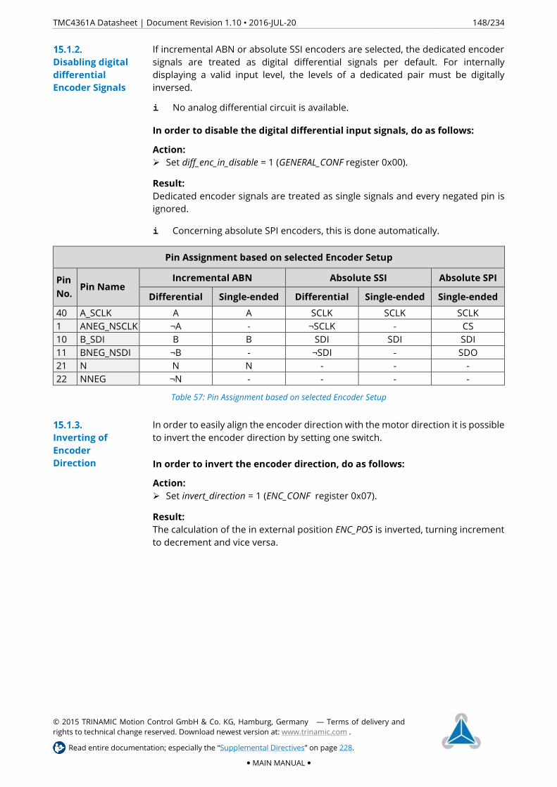
TMC4361A Datasheet | Document Revision 1.10 • 2016-JUL-20 148/234
© 2015 TRINAMIC Motion Control GmbH & Co. KG, Hamburg, Germany — Terms of delivery and
rights to technical change reserved. Download newest version at: www.trinamic.com .
Read entire documentation; especially the “Supplemental Directives” on page 228.
MAIN MANUAL
If incremental ABN or absolute SSI encoders are selected, the dedicated encoder
signals are treated as digital differential signals per default. For internally
displaying a valid input level, the levels of a dedicated pair must be digitally
inversed.
i No analog differential circuit is available.
In order to disable the digital differential input signals, do as follows:
Action: Set diff_enc_in_disable = 1 (GENERAL_CONF register 0x00).
Result: Dedicated encoder signals are treated as single signals and every negated pin is
ignored.
i Concerning absolute SPI encoders, this is done automatically.
Pin Assignment based on selected Encoder Setup
Pin No.
Pin Name Incremental ABN Absolute SSI Absolute SPI
Differential Single-ended Differential Single-ended Single-ended
40 A_SCLK A A SCLK SCLK SCLK
1 ANEG_NSCLK ¬A - ¬SCLK - CS
10 B_SDI B B SDI SDI SDI
11 BNEG_NSDI ¬B - ¬SDI - SDO
21 N N N - - -
22 NNEG ¬N - - - -
Table 57: Pin Assignment based on selected Encoder Setup
In order to easily align the encoder direction with the motor direction it is possible
to invert the encoder direction by setting one switch.
In order to invert the encoder direction, do as follows:
Action: Set invert_direction = 1 (ENC_CONF register 0x07).
Result: The calculation of the in external position ENC_POS is inverted, turning increment
to decrement and vice versa.
Disabling digital differential Encoder Signals
Inverting of Encoder Direction

TMC4361A Datasheet | Document Revision 1.10 • 2016-JUL-20 149/234
© 2015 TRINAMIC Motion Control GmbH & Co. KG, Hamburg, Germany — Terms of delivery and
rights to technical change reserved. Download newest version at: www.trinamic.com .
Read entire documentation; especially the “Supplemental Directives” on page 228.
MAIN MANUAL
If the encoder is installed correctly, the encoder values form a circle for one motor
revolution. Thus, the deviation ENC_POS_DEV between real position ENC_POS und
internal position XACTUAL forms a constant function over the whole motor
revolution.
Consequently, the resulting form of a deficiently installed encoder is oval-shaped.
This system failure results in a new function of ENC_POS_DEV that is similar to a
sine function. In Figure 58 A below, the position deviation is shown as function of
one motor revolution, which comprises 51200 microsteps.
TMC4361A provides an option to compensate this kind of misalignment by adding
a triangular shape function that counteracts the system error. This can improve
the encoder value evaluation significantly. Per default, this function is constant at
0.
In order to setup the triangular compensation function, do as follows:
Action: Set proper ENC_COMP_XOFFSET register 0x7D (15:0).
Set proper ENC_COMP_YOFFSET register 0x7D (23:16).
Set proper ENC_COMP_AMPL register 0x7D (31:24).
Result: ENC_COMP_XOFFSET is 16-bit register which represents a numeral figure between
0 and 1. The resulting offset on the abscissa is calculated by:
XOFF_LOW = ENC_COMP_XOFFSET · microsteps/rev / 65536.
A triangular function is generated, which has its lowest point at (XOFF_LOW; ENC_COMP_YOFFSET). The peak is shifted at a distance of half a revolution. The peak coordinate (XOFF_PEAK;YOFF_PEAK) is calculated as follows:
XOFF_PEAK = ENC_COMP_XOFFSET · microsteps/rev / 65536 + microsteps/rev / 2.
YOFF_PEAK = ENC_COMP_YOFFSET + ENC_COMP_AMPL.
In Figure 58 A, the red line illustrates this compensation function.
Internally, the triangular function is added to the ENC_POS value. As a result, the
position deviation is harmonized as a function of the motor revolution; which can
be seen in Figure 58 B.
Figure 61: Triangular Function that compensates Encoder Misalignments
-8
-6
-4
-2
0
2
4
6
8
0 10000 20000 30000 40000 50000
po
siti
on
de
viat
ion
µsteps
position deviation
compensation function
YOFF
AMPL
XOFF
A)
-8
-6
-4
-2
0
2
4
6
8
0 10000 20000 30000 40000 50000
po
siti
on
de
viat
ion
µsteps
position deviation
B)
Encoder Misalignment Compensation

TMC4361A Datasheet | Document Revision 1.10 • 2016-JUL-20 150/234
© 2015 TRINAMIC Motion Control GmbH & Co. KG, Hamburg, Germany — Terms of delivery and
rights to technical change reserved. Download newest version at: www.trinamic.com .
Read entire documentation; especially the “Supplemental Directives” on page 228.
MAIN MANUAL
Incremental ABN Encoder Settings
Incremental ABN encoders increment or decrement the external position counter register ENC_POS 0x50. This is based on A- and B-signal level transitions.
The external position register ENC_POS 0x50 is based on internal microsteps. Thus,
every AB transition is transferred to microsteps by a fixed constant value.
TMC4361A is able to calculated this constant automatically.
In order to configure the incremental ABN encoder constant automatically, do as follows:
Action: Set fullstep resolution of the motor in FS_PER_REV (STEP_CONF register 0x0A).
Set microstep resolution MSTEP_PER_FS (STEP_CONF register 0x0A).
Set encoder resolution – the number of AB transitions during one revolution -
in register ENC_IN_RES 0x54 (write access).
Result: The encoder constant value ENC_CONST (readable at register 0x54) is calculated
as follows:
ENC_CONST = MSTEP_PER_FS · FS_PER_REV / ENC_IN_RES
This constant is the number of microsteps through which ENC_POS is incremented
or decremented by one AB transition.
i ENC_CONST consists of 15 digits and 16 decimal places.
i In case 16 bits are not sufficient for a binary representation of the decimal
places, TMC4361A tries to match them to a multiple of 10000 within these 16
decimal places. Thereby, a perfect match can be achieved in case decimal
representation is preferred to a binary one.
i In case the decimal representation also does not fit completely, the type of
the decimal places of ENC_CONST can be selected manually with
ENC_IN_CONF (0). Set ENC_IN_CONF (0) to 0 for binary representation; or set it
to 1 for the decimal one. Keep in mind that with this approach ENC_POS can
slightly differ from the real position; especially the further away the position
moves from 0.
For some applications it can be useful to define the encoder constant value, which
in this case does not correspond to the number of microsteps per revolution; e.g.
if the encoder is not mounted directly on the motor.
In order to configure the incremental ABN encoder constant manually, do as follows:
Action: Set ENC_IN_RES(31) =1.
Set ENC_IN_CONF(0) to 0 for a binary or to 1 for a decimal representation as
explained in the previous section.
Set required encoder resolution in ENC_IN_RES (30:0) register 0x54.
Result: ENC_CONST consists of 15 digits and 16 decimal places. The constant is the
number of microsteps by which ENC_POS is incremented or decremented by one
AB transition.
Automatic Constant Configuration of Incremental ABN Encoder
Manual Constant Configuration of Incremental ABN Encoder

TMC4361A Datasheet | Document Revision 1.10 • 2016-JUL-20 151/234
© 2015 TRINAMIC Motion Control GmbH & Co. KG, Hamburg, Germany — Terms of delivery and
rights to technical change reserved. Download newest version at: www.trinamic.com .
Read entire documentation; especially the “Supplemental Directives” on page 228.
MAIN MANUAL
Incremental Encoders: Index Signal: N resp. Z
The index signal (N or Z channel) represents a recurrence of the same position in one motor encoder revolution. TMC4361A makes use of this signal to clear the external position counter, or to take a snapshot of the external or internal position, which then can be used to refine the home position more precisely.
Figure 62: Outline of ABN Signals of an incremental Encoder
Per default, the index channel is configured low active.
In order to set up high active polarity for the index channel, do as follows:
Action: Set pol_n =1 (register ENC_CONF 0x07).
Result: The index channel is high active.
The active polarity of the index channel can be used to clear the external position
counter or to take a snapshot of the external or internal position. Therefore,
N event is created internally. N event is based on the active polarity of the index
channel. As addition, they can also be based on the polarities of the
A and B channels.
Four active polarity configuration options for the index channel are available,
which are presented below. Configuration choice depends on customer-specific
design wishes.
In order to set up the index channel sensitivity based on active polarity, do as follows:
Action: Set n_chan_sensitivity (register ENC_CONF 0x07) to:
Index Channel Sensitivity
n_chan_sensitivity Result
b’00 N event is active in case index voltage level fits pol_n.
b’01 N event is triggered when the index channel switches to
active polarity.
b’10 N event is triggered when the index channel switches to
inactive polarity.
b’11 N event is triggered at both edges when the index
channel switches to either active or inactive polarity.
Table 58: Index Channel Sensitivity
A
B
t
Position -4 -3 -2 -1 0 5 64321 7
N
Setup of Active Polarity for Index Channel
Configuration of N Event
Index Channel
Sensitivity

TMC4361A Datasheet | Document Revision 1.10 • 2016-JUL-20 152/234
© 2015 TRINAMIC Motion Control GmbH & Co. KG, Hamburg, Germany — Terms of delivery and
rights to technical change reserved. Download newest version at: www.trinamic.com .
Read entire documentation; especially the “Supplemental Directives” on page 228.
MAIN MANUAL
It can be useful to specify A and B channel signal polarities for N event. Per default,
the polarities of both signal lines are set to 0 (low active).
In order to set up A channel polarity to high active for N event, do as follows:
Action: Set pol_a_for_n = 1 (ENC_CONF register 0x07).
Result: Now, A channel signal polarity for N event is high active.
In order to set up B channel polarity to high active for N event, do as follows:
Action: Set pol_b_for_n = 1 (ENC_CONF register 0x07).
Result: Now, B channel signal polarity for N event is high active.
In case A and B channel polarities do not have an influence on N event, both A
and B channel polarity signals can be ignored.
In order to ignore A and B channel polarities, do as follows:
Action: Set ignore_ab = 1 (ENC_CONF register 0x07).
Result: Now, the A and B channel signal polarities have no influence on N event.
N event can be used to clear the external position register ENC_POS 0x50. Two
choices are available: continous clearing and single clearing.
i Common practice is to clear to 0. However, TMC4361A offers the possibility
to clear to any single microstep count.
In order to set ENC_POS on N event to continuous clearing, do as follows:
Action: Set ENC_RESET_VAL register 0x51 to the requested microstep position.
Set clr_latch_cont_on_n = 1 (ENC_CONF register 0x07).
Set clear_on_n = 1 (ENC_CONF register 0x07).
Result: On every N event ENC_POS is set to ENC_RESET_VAL.
In order to only clear ENC_POS for the next N event, do as follows:
Action: Set ENC_RESET_VAL register 0x51 to the requested microstep position.
Set clr_latch_cont_on_n = 0 (ENC_CONF register 0x07).
Set clr_latch_once_on_n = 1 (ENC_CONF register 0x07).
Set clear_on_n = 1 (ENC_CONF register 0x07).
Result: When the next N event occurs, ENC_POS is set to ENC_RESET_VAL. After the
particular N event, clr_latch_once_on_n is automatically reset to 0.
A and B Channel
Signal Polarities
for N Event
External Position Counter ENC_POS
Clearing
ENC_POS
Continous
Clearing
ENC_POS Single
Clearing

TMC4361A Datasheet | Document Revision 1.10 • 2016-JUL-20 153/234
© 2015 TRINAMIC Motion Control GmbH & Co. KG, Hamburg, Germany — Terms of delivery and
rights to technical change reserved. Download newest version at: www.trinamic.com .
Read entire documentation; especially the “Supplemental Directives” on page 228.
MAIN MANUAL
N event can be used to latch external position register ENC_POS 0x50 to storage
register ENC_LATCH 0x51 (read access). Two choices are available: Continous
latching and single latching.
In order to continuously latch ENC_POS to ENC_LATCH on N event, do as follows:
Action: Set clr_latch_cont_on_n = 1 (ENC_CONF register 0x07).
Set latch_enc_on_n = 1 (ENC_CONF register 0x07).
Result: On every N event ENC_POS register 0x50 is latched to ENC_LATCH register 0x51.
In order to only latch ENC_POS to ENC_LATCH for the next N event, do as follows:
Action: Set clr_latch_cont_on_n = 0 (ENC_CONF register 0x07).
Set clr_latch_once_on_n = 1 (ENC_CONF register 0x07).
Set latch_enc_on_n = 1 (ENC_CONF register 0x07).
Result: When the next N event occurs, ENC_POS register 0x50 is latched to ENC_LATCH
register 0x51. After the particular N event, clr_latch_once_on_n is automatically
reset to 0.
N event can be used to latch internal position register X_ACTUAL 0x21 to storage
register X_LATCH 0x36 (read access). Two choices are available: Continous latching
and single latching.
In order to continuously latch X_ACTUAL to X_LATCH on N event, do as follows:
Action: Set clr_latch_cont_on_n = 1 (ENC_CONF register 0x07).
Set latch_enc_on_n = 1 (ENC_CONF register 0x07).
Set latch_x_on_n = 1 (ENC_CONF register 0x07).
Result: On every N event X_ACTUAL register 0x21 is latched to X_LATCH register 0x36.
In order to only latch X_ACTUAL to X_LATCH for the next N event, do as follows:
Action: Set clr_latch_cont_on_n = 0 (ENC_CONF register 0x07).
Set clr_latch_once_on_n = 1 (ENC_CONF register 0x07).
Set latch_enc_on_n = 1 (ENC_CONF register 0x07).
Set latch_x_on_n = 1 (ENC_CONF register 0x07).
Result: When the next N event occurs, X_ACTUAL register 0x21 is latched to X_LATCH
register 0x36. After the particular N event, clr_latch_once_on_n is automatically
reset to 0.
Latching External Position
Continous
Encoder Latching
Single Encoder
Latching
Latching Internal Position
Continous
Latching
Single Latching

TMC4361A Datasheet | Document Revision 1.10 • 2016-JUL-20 154/234
© 2015 TRINAMIC Motion Control GmbH & Co. KG, Hamburg, Germany — Terms of delivery and
rights to technical change reserved. Download newest version at: www.trinamic.com .
Read entire documentation; especially the “Supplemental Directives” on page 228.
MAIN MANUAL
Absolute Encoder Settings
Serial encoders provide absolute encoder angle data in contrast to step transitions, which are delivered from incremental encoders. TMC4361A provides an external clock for the encoder in order to trigger serial data input,
TMC4361A offers singleturn and multiturn options for the serial data stream
interpretation. Per default, multiturn data is not enabled. In case multiturn data
is enabled, it is interpreted as unsigned count of revolutions.
In case multiturn encoder data is transmitted, do as follows:
Action: Set multi_turn_in_en = 1 (ENC_CONF register 0x07).
OPTIONAL CONFIGURATION: Set multi_turn_in_signed = 1.
In case multiturn data is provided as signed count of encoder revolutions.
Result: Data from connected encoders are interpreted as multiturn data.
In case only singleturn data is transmitted TMC4361A is able to permanently
calculate internally the number of encoder revolutions as if it where externally
transferred multiturn data.
In case singleturn encoder data is transmitted but internally multiturn data is required, do as follows:
Action: Set multi_turn_in_en = 0 (ENC_CONF register 0x07).
Set calc_multi_turn_behav = 1 (ENC_CONF register 0x07).
Result: Data from connected singleturn encoders is internally transferred to multiturn
data.
NOTE:
Multiturn calculations are only correct in case two consecutive singleturn data
values differ only by one step less than a half turn difference, or even less.
Singleturn or Multiturn Data

TMC4361A Datasheet | Document Revision 1.10 • 2016-JUL-20 155/234
© 2015 TRINAMIC Motion Control GmbH & Co. KG, Hamburg, Germany — Terms of delivery and
rights to technical change reserved. Download newest version at: www.trinamic.com .
Read entire documentation; especially the “Supplemental Directives” on page 228.
MAIN MANUAL
The external position register ENC_POS 0x50 is based on internal microsteps. Thus,
every input data angle is transferred to microsteps by a fixed constant value.
TMC4361A is able to automatically calculate this constant.
In order to configure the absolute encoder constant automatically, do as follows:
Action: Set fullstep resolution of the motor in FS_PER_REV (STEP_CONF register 0x0A).
Set microstep resolution MSTEP_PER_FS (STEP_CONF register 0x0A).
Set encoder resolution in register ENC_IN_RES 0x54 (write access).
Result: The encoder constant value ENC_CONST (readable at register 0x54) is calculated
as follows:
ENC_CONST = MSTEP_PER_FS · FS_PER_REV / ENC_IN_RES
The external position ENC_POS 0x50 is calculated by multiplying the constant with
the transmitted input angle.
i ENC_CONST consists of 15 digits and 16 decimal places.
i In contrast to incremental ABN encoders, ENC_CONST is always represented
as binary constant.
For some applications it can be useful to define the encoder constant value, which
in this case does not correspond to the number of microsteps per revolution;
e.g. if the encoder is not mounted directly on the motor.
In order to configure the absolute encoder constant manually, do as follows:
Action: Set ENC_IN_RES (31) =1.
Set required encoder resolution in ENC_IN_RES (30:0) register 0x54.
Result: ENC_CONST consists of 15 digits and 16 decimal places. The external position
ENC_POS 0x50 is calculated by multiplying the constant with the transmitted input
angle.
Automatic Constant Configuration of Absolute Encoder
Manual Constant Configuration of incremental ABN Encoder
TMC4361A Datasheet | Document Revision 1.10 • 2016-JUL-20 156/234
© 2015 TRINAMIC Motion Control GmbH & Co. KG, Hamburg, Germany — Terms of delivery and
rights to technical change reserved. Download newest version at: www.trinamic.com .
Read entire documentation; especially the “Supplemental Directives” on page 228.
MAIN MANUAL
Encoder Data must be maintained correctly. Consequently, certain settings must
be configured so that TMC4361A displays them as specified.
In order to configure absolute encoder data, do as follows:
Action: Set SINGLE_TURN_RES (ENC_IN_DATA register 0x08) to the number of singleturn
data bits -1.
OPTION A1: IF MULTITURN DATA IS TRANSMITTED
Set MULTI_TURN_RES (ENC_IN_DATA register 0x08) to the number of
multiturn data bits -1.
OR OPTION A2: IF MULTITURN DATA IS NOT TRANSMITTED
Set MULTI_TURN_RES = 0 (ENC_IN_DATA register 0x08).
Set STATUS_BIT_CNT (ENC_IN_DATA register 0x08) to the number of status bits.
OPTION B1: IF STATUS FLAGS ARE ORDERED IN FRONT
Set left_aligned_data = 0 (ENC_IN_CONF register 0x07).
OR OPTION B2: IF STATUS FLAGS ARE ORDERED IN FRONT
Set left_aligned_data = 1 (ENC_IN_CONF register 0x07).
Result: SINGLE_TURN_RES defines the most significant bit (MSB) of the angle data bits,
whereas MULTI_TURN_RES defines the MSB of the revolution counter bits. Up to
three status bits can be received. The number of transferred clock bits that are
sent to the encoder is calculated as follows:
#SCLK Cycles= (SINGLE_TURN_RES+1) + (MULTI_TURN_RES+1) + STATUS_BIT_CNT
Also, the order in which the status bits occur in one encoder data stream can be
configured. In Figure 59 on the next page, example setups are depicted.
NOTE:
In case more than three status bits or additional fill bits are sent from the encoder,
clock errors can occur because the number of transferred clock bits does not fit.
In order to prevent clock failures, MULTI_TURN_RES can be set to a higher value
than otherwise required; even if the encoder does not provide multiturn data. This
can result in erroneous multiturn data, which can be corrected by setting
multi_turn_in_en=0 in order to skip multiturn data automatically.
In order to compensate unavailable multiturn data make use of
calc_multi_turn_behav, as explained in section 15.4.1 on page 154.
Turn page for serial data output examples.
Absolute Encoder Data Setup

TMC4361A Datasheet | Document Revision 1.10 • 2016-JUL-20 157/234
© 2015 TRINAMIC Motion Control GmbH & Co. KG, Hamburg, Germany — Terms of delivery and
rights to technical change reserved. Download newest version at: www.trinamic.com .
Read entire documentation; especially the “Supplemental Directives” on page 228.
MAIN MANUAL
Figure 63:Serial Data Output: Four Examples
Key:
a) SINGLE_TURN_RES=6; MULTI_TURN_RES=4; STATUS_BIT_CNT=0; left_aligned_data=0
b) SINGLE_TURN_RES=6; MULTI_TURN_RES=0; STATUS_BIT_CNT=2; left_aligned_data=0
c) SINGLE_TURN_RES=5; MULTI_TURN_RES=4; STATUS_BIT_CNT=1; left_aligned_data=0
d) SINGLE_TURN_RES=4; MULTI_TURN_RES=2; STATUS_BIT_CNT=3; left_aligned_data=1
For some applications it can be useful to limit the difference between two
consecutive encoder data values; for instance, if encoder data lines are subject to
too much noise.
Per default, encoder data values can show a difference of 1/8th per encoder
revolution, only if the limitation is enabled. The difference can be configured to a
smaller value, if necessary.
In order to enable and configure encoder data variation limitation, do as follows:
Action: OPTIONAL: Set proper SER_ENC_VARIATION register 0x63 (7:0).
Set serial_enc_variation_limit =1 (ENC_IN_CONF register 0x07).
Result: The encoder data value that is received subsequently must not exceed the
previous data more than:
Maximum tolerated deviation = SER_ENC_VARIATION / 256 · 1/8 · ENC_IN_RES.
In case the variation exceeds the above mentioned limit, the new data value is
rejected internally and the status flag SER_ENC_DATA_FAIL is raised.
i In case SER_ENC_VARIATION = 0, the limit is defined by 1/8 · ENC_IN_RES.
Serial data
outMSBM LSBM MSBS LSBS
Serial data
outSB1 SB0 MSBS LSBS
a) A1+B1:
Serial data
outSB0 MSBM LSBM MSBS LSBS
Serial data
outMSBM LSBM MSBS LSBS SB2 SB1 SB0
b) A2+B1:
c) A1+B1:
d) A1+B2:
Emitting Encoder Data Variation

TMC4361A Datasheet | Document Revision 1.10 • 2016-JUL-20 158/234
© 2015 TRINAMIC Motion Control GmbH & Co. KG, Hamburg, Germany — Terms of delivery and
rights to technical change reserved. Download newest version at: www.trinamic.com .
Read entire documentation; especially the “Supplemental Directives” on page 228.
MAIN MANUAL
SSI Clock Generation
In order to receive encoder data from the absolute encoder, TMC4361A generates clock patterns according to SSI standard. Data transfer is initiated by switching the clock line SCLK from high to low level. The transfer starts with the next rising edge of SCLK. The number of emitted clock cycles depends on the expected data width, as explained in section 15.4.4.
One clock cycle has a high and a low phase, which can be defined separately
according to internal clock cycles. Per default, sample points of serial data are set
at the falling edges of SCLK. Some encoders need more clock cycles – than are
available during the low clock phase – in order to prepare data for transfer. Also,
due to long wires, data transfer can take more time. To counteract the above
mentioned issues, the delay time SSI_IN_CLK_DELAY (default value equals 0) for
compensation can be specified in order to prolong the sampling start. Therefore,
this delay configuration can automatically generate more clock cycles.
After a data request – when all clock cycles have been emitted – the serial clock
must remain idle for a certain interval before the next request is automatically
initiated. This interval SER_PTIME can also be configured in internal clock cycles.
i According to SSI standard, select an interval that is longer than 21 µs.
In order to configure the SSI clock generation, do as follows:
Action: Set SINGLE_TURN_RES (ENC_IN_DATA register 0x08) to the number of singleturn
data bits -1.
Set MULTI_TURN_RES (ENC_IN_DATA register 0x08) to the number of multiturn
data bits -1 in case multiturn data is enabled and used.
Set STATUS_BIT_CNT (ENC_IN_DATA reg. 0x08) to the number of status bits.
Set proper left_aligned_data (ENC_IN_CONF register 0x07).
Set proper SER_CLK_IN_LOW (register 0x56) in internal clock cycles.
Set proper SER_CLK_IN_HIGH (register 0x56) in internal clock cycles.
OPTIONAL CONFIG: Set proper SSI_IN_CLK_DELAY (register 0x57) in internal
clock cycles.
OPTIONAL CONFIG: Set proper SER_PTIME (reg. 0x58) in internal clk cycles.
Finally, set serial_enc_in_mode = b’01.
Result: TMC4361A emits serial clock streams at SCLK in order to receive absolute encoder
data at SDI. If SSI_IN_CLK_DELAY > 0, the SDI sample points are delayed (see figures
below). SER_PTIME defines the interval between two consecutive data requests.
i If differential encoder is selected, the negated clock emits at ¬SCLK; and ¬SDI
is also evaluated.
Figure 64: SSI: SSI_IN_CLK_DELAY=0
Figure 65: SSI: SSI_IN_CLK_DELAY>SER_CLK_IN_HIGH
LSBMSB
Sample points
Serial data in
Serial clock
out
SER_CLK_IN_HIGH SER_CLK_IN_LOW
MSB LSB---
Sample points
Serial data in
Serial clock
out
SSI_IN_CLK_DELAY
Configuration Details

TMC4361A Datasheet | Document Revision 1.10 • 2016-JUL-20 159/234
© 2015 TRINAMIC Motion Control GmbH & Co. KG, Hamburg, Germany — Terms of delivery and
rights to technical change reserved. Download newest version at: www.trinamic.com .
Read entire documentation; especially the “Supplemental Directives” on page 228.
MAIN MANUAL
If safe transmission must be determined, it is possible to send a second request
so that the encoder repeats the same encoder data. Therefore, a second interval
SSI_WTIME must be defined.
i According to SSI standard, select an interval that is shorter than 19 µs.
In order to enable multicycle requests, do as follows:
Action: Set ssi_multi_cycle_data =1 (ENC_IN_CONF register 0x07).
Set proper SSI_WTIME (register 0x57) in internal clk cycles.
Result: After a data request – when all clock cycles have been emitted – the serial clock
remains idle for SSI_WTIME clock cycles. Afterwards, the second request is
automatically initiated to receive the same encoder data. If the second encoder
data differs from the first one, error flag MULTI_CYCLE_FAIL (register 0x0F) and
error event SER_ENC_DATA_FAIL (register 0x0E) is generated.
After the second data request, the next interval lasts SER_PTIME clock cycles to
request new encoder data.
Several but not all SSI encoders emit angle data, which is gray-encoded.
TMC4361A is able to decode this data automatically.
In order to enable gray-encoded angle data, do as follows:
Action: Set ssi_gray_code_en =1 (ENC_IN_CONF register 0x07).
Result: Encoder data is recognized as gray-encoded and thus also decoded accordingly.
Enabling Multicycle SSI request
Gray-encoded SSI Data Streams

TMC4361A Datasheet | Document Revision 1.10 • 2016-JUL-20 160/234
© 2015 TRINAMIC Motion Control GmbH & Co. KG, Hamburg, Germany — Terms of delivery and
rights to technical change reserved. Download newest version at: www.trinamic.com .
Read entire documentation; especially the “Supplemental Directives” on page 228.
MAIN MANUAL
SPI Encoder Data Evaluation
SPI encoder interfaces typically consist of four signal lines. In addition to SSI encoder signal lines (SCLK, MISO), a chip select line (CS) and a data input (MOSI) to the master is provided.
The number of bits per transfer is calculated automatically; based on proper
multi_turn_in_en, SINGLE_TURN_RES, MULTI_TURN_RES, and STATUS_BIT_CNT, as
explained in sections 15.4.1 (page 154) and 15.4.4 (page 156).
A typical SPI communication process responds to any SPI data transfer request
when the next transmission occurs. When TMC4361A receives an answer from
the encoder, it calculates ENC_POS immediately. The encoder slave does not send
any data without receiving a request first.
Therefore, TMC4361A always sends ADDR_TO_ENC value to request encoder data
from the SPI encoder slave device. The LSB of the serial data output is
ADDR_TO_ENC (0).
Received encoder data is stored in ADDR_FROM_ENC. Thus, encoder values can be
verified and compared to microcontroller data later on.
i The clock generation works similarly to SSI clock generation, as described in
section 15.4.5 on page 158; based on proper SER_CLK_IN_HIGH,
SER_CLK_IN_LOW, and SER_PTIME.
In order to configure a basic SPI communication procedure, do as follows:
Action: Set SINGLE_TURN_RES (ENC_IN_DATA register 0x08) to the number of singleturn
data bits -1.
Set MULTI_TURN_RES (ENC_IN_DATA register 0x08) to the number of multiturn
data bits -1 in case multiturn data is enabled and used.
Set STATUS_BIT_CNT (ENC_IN_DATA register 0x08) to the number of status bits.
Set proper left_aligned_data (ENC_IN_CONF register 0x07).
Set correct SPI transfer mode that is described in the next section.
Set ADDR_TO_ENC register 0x68 to the specified SPI encoder address that
contains angle data.
Set proper SER_CLK_IN_LOW (register 0x56) in internal clock cycles.
Set proper SER_CLK_IN_HIGH (register 0x56) in internal clock cycles.
OPTIONAL CONFIG: Set proper SER_PTIME (register 0x58) in internal clk cycles.
Finally, set serial_enc_in_mode = b’11.
Result: TMC4361A emits serial clock streams at SCLK in order to receive absolute encoder
data at SDI pin. The number of generated clock cycles depends on
SINGLE_TURN_RES, MULTI_TURN_RES, and STATUS_BIT_CNT.
Pin ANEG_NSCLK functions as negated chip select line for the SPI encoder that is
generated according to the serial clock and the selected SPI mode; which is
described in the next section.
Pin BNEG_NSDI is the MOSI line that transfers SPI datagrams to the SPI encoder.
Datagrams, which are transferred permanently to receive angle data, consists of
ADDR_TO_ENC data.
SER_PTIME defines the interval between two consecutive data requests.
Turn page for information on SPI mode selection.
SPI Encoder Communication Process

TMC4361A Datasheet | Document Revision 1.10 • 2016-JUL-20 161/234
© 2015 TRINAMIC Motion Control GmbH & Co. KG, Hamburg, Germany — Terms of delivery and
rights to technical change reserved. Download newest version at: www.trinamic.com .
Read entire documentation; especially the “Supplemental Directives” on page 228.
MAIN MANUAL
Per default, SPI encoder data transfer is managed in the same way as the
communication between microcontroller and TMC4361A. TMC4361A supports all
four SPI modes with proper setting of switches spi_low_before_cs and
spi_data_on_cs.
THE PROCESS IS AS FOLLOWS:
By setting spi_low_before_cs = 0, negated chip select line at ANEG_NSCLK is
switched to active low before the serial clock line SCLK switches.
By setting spi_low_before_cs = 1, negated chip select line at ANEG_NSCLK is
switched to active low after the serial clock line SCLK switches.
By setting spi_data_on_cs = 0, the first data bit at BNEG_NSDI is changed at the
same time as the first slope of the serial clock SCLK.
By setting spi_data_on_cs = 1, the first data bit at BNEG_NSDI is changed at the
same time as the negated chip select signal at BNEG_NSDI switches to active level.
In the table below, all four SPI modes are presented.
Per default, the delay between serial clock line and negated chip select line has a
time frame of either SER_CLK_IN_HIGH or SER_CLK_IN_LOW clock cycles, which
depends on the actual voltage level of the serial clock.
This particular interval does not always match the encoder behavior perfectly.
Therefore, both the first and last intervals between the serial clock line and the
negated chip select line can be specified separately in clock cycles at
SSI_IN_CLK_DELAY register 0x57.
Below, the SSI_IN_CLK_DELAY interval is highlighted in red in all four diagrams.
Supported SPI Encoder Data Transfer Modes
spi_low_before_cs:
spi_data_on_cs
0 1
0
1
Table 59: Supported SPI Encoder Data Transfer Modes
Sample points
(B_SDI)
Serial data out
(BNEG_NSDI)
Serial clock out
(A_SCLK)
Chip Select
(ANEG_NSCLK)
MSB LSB
Sample points
(B_SDI)
Serial data out
(BNEG_NSDI)
Serial clock out
(A_SCLK)
Chip Select
(ANEG_NSCLK)
MSB LSB
Sample points
(B_SDI)
Serial data out
(BNEG_NSDI)
Serial clock out
(A_SCLK)
Chip Select
(ANEG_NSCLK)
MSB LSB
Sample points
(B_SDI)
Serial data out
(BNEG_NSDI)
Serial clock out
(A_SCLK)
Chip Select
(ANEG_NSCLK)
MSB LSB
SPI Encoder Mode Selection

TMC4361A Datasheet | Document Revision 1.10 • 2016-JUL-20 162/234
© 2015 TRINAMIC Motion Control GmbH & Co. KG, Hamburg, Germany — Terms of delivery and
rights to technical change reserved. Download newest version at: www.trinamic.com .
Read entire documentation; especially the “Supplemental Directives” on page 228.
MAIN MANUAL
SPI Encoder Configuration via TMC4361A
Connected SPI encoder can be configured via TMC4361A., which renders a connection between microcontroller and encoder unnecessary.
A configuration request is sent using the settings of SERIAL_ADDR_BITS and
SERIAL_DATA_BITS, which define the transferring bit numbers.
In order to prepare SPI encoder configuration procedures, do as follows:
Action: Set SERIAL_ADDR_BITS (ENC_IN_DATA register 0x08) to the number of address
bits of any SPI encoder configuration datagram.
Set SERIAL_DATA_BITS (ENC_IN_DATA register 0x08) to the number of data bits
of any SPI encoder configuration datagram.
Result: In case configuration data is transferred to the SPI encoder, SERIAL_ADDR_BITS bits
and SERIAL_DATA_BITS bits are sent in two SPI configuration datagrams; exactly in
this order.
Because encoder data requests occur as an endless stream, it is necessary to
interrupt data requests when a configuration request occurs. Consequently, a
handshake behavior is implemented.
In order to transfer configuration data to the SPI encoder, do as follows:
Action: Set DATA_TO_ENC register 0x69 to any value.
Set ADDR_TO_ENC register 0x68 to the configuration address of the SPI encoder.
Set DATA_TO_ENC register 0x69 to the configuration data of the SPI encoder.
Result: The first DATA_TO_ENC access stops the repetitive encoder data request.
After the second DATA_TO_ENC access, three datagrams are sent to SPI encoder:
1. One address datagram is transmitted, which contains the ADDR_TO_ENC value.
Data that is received simultaneously with the request is not stored.
2. One data datagram is transmitted that contains the DATA_TO_ENC value. Data
that is received simultaneously with the request is stored in ADDR_FROM_ENC
register 0x6A because this is the response of the ADDR_TO_ENC request.
3. One no-operation datagram (NOP) is transmitted. Data that is received
simultaneously with the request is stored in DATA_FROM_ENC register 0x6B
because this is the response of the DATA_TO_ENC request.
In order to finalize the configuration procedure and continue with the encoder data requests, do as follows:
Read out ADDR_FROM_ENC register 0x6A first.
Set ADDR_TO_ENC register 0x68 to the specified SPI encoder address that
contains angle data.
Obligatory at finalization: Read out DATA_FROM_ENC register 0x6B.
Result: The configuration request data is read out. After DATA_FROM_ENC register readout,
the encoder data request stream of angle data continues.
SPI Encoder Configuration Communication Process

TMC4361A Datasheet | Document Revision 1.10 • 2016-JUL-20 163/234
© 2015 TRINAMIC Motion Control GmbH & Co. KG, Hamburg, Germany — Terms of delivery and
rights to technical change reserved. Download newest version at: www.trinamic.com .
Read entire documentation; especially the “Supplemental Directives” on page 228.
MAIN MANUAL
16. Possible Regulation Options with Encoder Feedback
Beyond simple feedback monitoring, encoder feedback can be used for controlling motion controller outputs in such a way that the internal actual position matches or follows the real position ENC_POS. Two options are provided: PID control and closed-loop operation. Closed-loop operation is preferable if the encoder is mounted directly on the back of the motor and position data is evaluated precisely. PID control is preferable if the encoder is located on the drive side with no fixed connection between motor and drive side; e.g. belt drives.
Closed-Loop and PID Registers
Register Name Register address Remarks
ENC_IN_CONF 0x07 RW Encoder configuration register: Closed-Loop
configuration switches.
CL_TR_TOLERANCE 0x51 R Absolute tolerated deviation to trigger
TARGET_REACHED during regulation.
ENC_POS_DEV 0x52 R Deviation between XACTUAL and ENC_POS.
Closed-Loop and PID
Register Set
0x59…5F
0x60…61 W Closed-Loop and PID configuration parameters.
Encoder velocity
configuration 0x63 W Encoder velocity filter configuration parameters.
Encoder velocity 0x65
0x66 R
Current encoder velocity (signed).
Current filtered encoder velocity (signed).
Table 60: Dedicated Closed-Loop and PID Registers
Based on the difference ENC_POS_DEV (readout at register 0x52) between internal
position XACTUAL and external position ENC_POS, a status flag ENC_FAIL_F and a
corresponding error event ENC_FAIL is generated automatically.
In order to set a tolerated position mismatch, do as follows:
Action: Set ENC_POS_DEV_TOL register 0x53 to the maximum microstep value that
represents no mismatch failure.
Result: In case |ENC_POS_DEV| ≤ ENC_POS_DEV_TOL, no encoder failure flag is set.
In case |ENC_POS_DEV| > ENC_POS_DEV_TOL, ENC_FAIL_Flag is set.
i At this point, the corresponding encoder event ENC_FAIL is also triggered.
In case one of the regulation modes is selected, TARGET_REACHED event and
status flag is only released when:
XACTUAL = XTARGET and |ENC_POS_DEV| ≤ CL_TR_TOLERANCE.
Consequently, CL_TR_TOLERANCE register 0x52 (only write access) is the maximal
tolerated position mismatch for target reached status.
Feedback Monitoring
Target-Reached during Regulation

TMC4361A Datasheet | Document Revision 1.10 • 2016-JUL-20 164/234
© 2015 TRINAMIC Motion Control GmbH & Co. KG, Hamburg, Germany — Terms of delivery and
rights to technical change reserved. Download newest version at: www.trinamic.com .
Read entire documentation; especially the “Supplemental Directives” on page 228.
MAIN MANUAL
Based on a position difference error PID_E = XACTUAL – ENC_POS the
PID (proportional integral differential) controller calculates a signed velocity value
(vPID), which is used for minimizing the position error. During this process,
TMC4361A moves with vPID until |PID_E| – PID_TOLERANCE ≤ 0 is reached and the
position error is removed.
vPID is calculated by:
𝑣𝑃𝐼𝐷 =𝑃𝐼𝐷_𝑃
256∙ 𝑃𝐼𝐷_𝐸 ∙ [
1
𝑠] +
𝑃𝐼𝐷_𝐼
256 ∙ ∫ 𝑃𝐼𝐷_𝐸 ∙ 𝑑𝑡
𝑡
0
+ 𝑃𝐼𝐷_𝐷 ∙ 𝑃𝐼𝐷_𝐸 ∙𝑑
𝑑𝑡
𝑣𝑃𝐼𝐷 =𝑃𝐼𝐷_𝑃
256∙ 𝑃𝐼𝐷_𝐸 ∙ [
1
𝑠] +
𝑃𝐼𝐷_𝐼
256 ∙ 𝑃𝐼𝐷_𝐼𝑆𝑈𝑀 + 𝑃𝐼𝐷_𝐷 ∙ 𝑃𝐼𝐷_𝐸 ∙
𝑑
𝑑𝑡
𝑣𝑃𝐼𝐷 =𝑃𝐼𝐷_𝑃
256∙ 𝑃𝐼𝐷_𝐸 ∙ [
1
𝑠] +
𝑃𝐼𝐷_𝐼
256 ∙ 𝑃𝐼𝐷_𝐸 ∙
𝑓𝐶𝐿𝐾
128+ 𝑃𝐼𝐷_𝐷 ∙ 𝑃𝐼𝐷_𝐸 ∙
𝑑
𝑑𝑡
Key:
PID_P = proportional term; PID_I = integral term; PID_D = derivate term
The following parameters can be read out during PID operation.
Actual PID output velocity.
Actual PID position deviation between XACTUAL and ENC_POS.
Actual PID integrator sum (update frequency: fCLK/128), which is calculated by:
PID_ISUM=PID_E · fCLK /128
Turn page for information on configuration of PID regulation.
PID-based Control of XACTUAL
PID Readout Parameters
PID_VEL 0x5A
PID_E 0x5D
PID_ISUM 0x5B

TMC4361A Datasheet | Document Revision 1.10 • 2016-JUL-20 165/234
© 2015 TRINAMIC Motion Control GmbH & Co. KG, Hamburg, Germany — Terms of delivery and
rights to technical change reserved. Download newest version at: www.trinamic.com .
Read entire documentation; especially the “Supplemental Directives” on page 228.
MAIN MANUAL
In order to set parameters and clipping values for PID regulation correctly,
consider the following details:
Large velocity variations are avoided by limiting vPID value with PID_DV_CLIP
(register 0x5E). This clipping parameter limits both vPID and PID_VEL.
The error sum PID_ISUM (read out at 0x5B) is generated by the integral term.
PID_ISUM is limited by setting PID_I_CLIP register 0x5D.
i The maximum value of PID_I_CLIP must meet the condition
PID_I_CLIP ≤ PID_DV_CLIP / PID_I.
i If the error sum PID_ISUM is not clipped, it is increased with each time step by
PID_I · PID_E. This continues as long as the motor does not follow.
Time scaling for deviation (with respect to error correction periods) is controlled
by PID_D_CLKDIV register.
i During error correction, fixed clock frequency fPID_INTEGRAL is valid:
fPID_INTEGRAL[Hz] = fCLK[Hz] / 128
The internal velocity VEL_ACT_PID alters actual ramp velocity VACTUAL. Two
settings are provided:
In case regulation_modus = b’11, VACTUAL is assigned as pulse generator base value
and VEL_ACT_PID is calculated by VEL_ACT_PID = VACTUAL + vPID.
In case regulation_modus = b’10, zero is assigned as pulse generator base value.
Now, VEL_ACT_PID = vPID is valid.
TMC4361A provides the programmable hysteresis PID_TOLERANCE for target
position stabilization; which avoids oscillations through error correction in case
XACTUAL is close to the real mechanical position.
The PID controller of TMC4361A is programmable up to approximate 100 kHz
update rate (at fCLK = 16 MHz). This high speed update rate qualifies PID regulation
for motion stabilization.
Now that PID control parameters and clipping values are configured, as explained
above, PID regulation can be enabled. Two options can be selected.
In order to enable PID control, do as follows:
Action:
OPTION 1: BASE PULSE GENERATOR VELOCITY = 0
Set regulation_modus = b’10 (ENC_IN_CONF register 0x07).
OPTION 2: BASE PULSE GENERATOR VELOCITY = VACTUAL
Set regulation_modus = b’11 (ENC_IN_CONF register 0x07).
Result: PID regulation is enabled.
NOTE
Detailed knowledge of a particular application (including dynamics of mechanics)
is necessary for PID controller parameterization.
PID Control Parameters and Clipping Values
PID_DV_CLIP 0x5E
PID_I_CLIP
0x5D (14:0)
PID_D_CLKDIV
0x5D (23:16)
VEL_ACT_PID
PID_TOLERANCE
0x5F
Enabling PID Regulation

TMC4361A Datasheet | Document Revision 1.10 • 2016-JUL-20 166/234
© 2015 TRINAMIC Motion Control GmbH & Co. KG, Hamburg, Germany — Terms of delivery and
rights to technical change reserved. Download newest version at: www.trinamic.com .
Read entire documentation; especially the “Supplemental Directives” on page 228.
MAIN MANUAL
Closed-Loop Operation
The closed-loop unit of TMC4361A directly modifies output currents and Step/Dir outputs of the internal step generator; which is dependent on the feedback data. The 2-phase closed-loop control of TMC4361 follows a different approach than Field-Oriented Control (FOC); which is similar to PID control cascades. The ramp generator, which assigns target and velocity, is independent of position control (commutation angle control); which is also independent of current control. Closed-loop operation can only be used in combination with 256 microsteps per fullstep.
Closed-loop does not control current values via the internal step generator. The
currents values at the SPI output and the Step/Dir outputs are verified using the
evaluated difference between internal position XACTUAL and external position
ENC_POS; considering the calibrated offset parameter CL_OFFSET.
In order to set parameters and clipping values for closed-loop regulation correctly,
consider the following details:
This register contains the basic offset value between internal and external
position during calibration process, which is necessary for closed-loop operation,
and offers read-write access. The write access can be used if a defined fixed offset
value is preferred, which is verified beforehand.
The continuously updated parameter ENC_POS_DEV displays the deviation
between XACTUAL and ENC_POS; considering CL_OFFSET.
CL_BETA is the maximum commutation angle that is used to compensate an
evaluated deviation ENC_POS_DEV. In case the deviation reaches CL_BETA value, the
commutation angle remains stable at this value to follow the overload. Also,
CL_MAX event is triggered at this point.
This parameter is set to select the tolerance range for position deviation. In case
|ENC_POS_DEV| ≤ CL_TOLERANCE, CL_FIT_F lag becomes set.
In case a mismatch between internal and external position occurs, CL_FIT event is
triggered to signify when the mismatch is removed.
CL_DELTA_P is a proportional controller that compensates a detected position
deviation between internal and external position. See also Figure 63, page 167.
In case |ENC_POS_DEV| ≤ CL_TOLERANCE, CL_DELTA_P is automatically set to 1.0.
In case |ENC_POS_DEV| > CL_TOLERANCE, the closed-loop unit of TMC4361A
multiplies ENC_POS_DEV with CL_DELTA_P and adds the resulting value to the
current ENC_POS. Thus, a current commutation angle for higher stiffness
position maintenance, which is clipped at CL_BETA, is calculated.
i CL_DELTA_P consists of 24 bits. The last 16 bits represent decimal places. The
final proportional term is thus calculated by: pPID = CL_DELTA_P / 65536.
i Therefore, the higher pPID the faster the reaction on position deviations.
NOTE:
A high pPID term can lead to oscillations that must be avoided.
In case, one absolute encoder is connected, this value represents the delay time
in numbers of clock cycles between two consecutive regulation cycles. It is
recommended to adjust this value to the regulation cycle; which is either equal or
slower than the encoder request rate. In case incremental ABN encoder is
selected, this value is automatically set to fetch the fastest possible regulation
rate; which in most cases are five clock cycles.
Basic Closed-Loop Parameters
CL_OFFSET 0x59
ENC_POS_DEV
0x52
CL_BETA
0x1C (8:0)
CL_TOLERANCE
0x5F (7:0)
CL_DELTA_P 0x5C
CL_CYCLE 0x63
(31:16)

TMC4361A Datasheet | Document Revision 1.10 • 2016-JUL-20 167/234
© 2015 TRINAMIC Motion Control GmbH & Co. KG, Hamburg, Germany — Terms of delivery and
rights to technical change reserved. Download newest version at: www.trinamic.com .
Read entire documentation; especially the “Supplemental Directives” on page 228.
MAIN MANUAL
ENC_POS_DEV [µSteps]
New output angle
ENC_POS+45°
(+128 µSteps)
ENC_POS+90°
(+256 µSteps)
ENC_POS-90°
(-256 µSteps)
ENC_POS-45°
(-128 µSteps)
128
(45°)
256
(90°)
384
(135°)
-128
(-45°)
-256
(-90°)
-384
(-135°)
pPID = 1pPID = 1
pPID = 2
pPID = 2
pPID = 4
pPID = 4
0°
–CL_TOLERANCE
CL_TOLERANCE
CL_BETA
–CL_BETA
Figure 66: Calculation of the Output Angle with appropriate CL_DELTA_P
Now that basic closed-loop control parameters are configured, as explained
above, closed-loop regulation can be enabled.
i The presented calibration process is very basic. Refer to the closed-loop
Application Note for detailed calibration process information.
In order to enable and calibrate closed-loop control, do as follows:
PRECONDITION: SET TO BEST POSSIBLE MAXIMUM CURRENT SCALING
PROCEED WITH: OPTION 1: CL_OFFSET IS GENERATED DURING CALIBRATION
Action:
Set MSTEPS_PER_FS = 0 (STEP_CONF register 0x0A) [256 microsteps per fullstep].
Move to any fullstep position (MSCNT mod 128 = 0).
Set regulation_modus = b’01 (ENC_IN_CONF register 0x07).
Set cl_caclibration_en =1 (ENC_IN_CONF register 0x07).
Wait for a defined time span (system settle down).
Set cl_caclibration_en =0 (ENC_IN_CONF register 0x07).
Result: Closed-loop operation is enabled with basic calibration. CL_OFFSET is set to
position mismatch during calibration process.
OR PROCEED WITH OPTION 2: CL_OFFSET IS USED FOR CALIBRATION
In case CL_OFFSET was saved and no position loss has occurred while closed-loop
operation was disabled, it can be used to replace the calibration process.
Action: Set MSTEPS_PER_FS = 0 (STEP_CONF register 0x0A) [256 microsteps per fullstep].
Set regulation_modus = b’01 (ENC_IN_CONF register 0x07).
Set CL_OFFSET to any preferred microstep value.
Result: Closed-loop operation is enabled.
Enabling and calibrating Closed-Loop Operation

TMC4361A Datasheet | Document Revision 1.10 • 2016-JUL-20 168/234
© 2015 TRINAMIC Motion Control GmbH & Co. KG, Hamburg, Germany — Terms of delivery and
rights to technical change reserved. Download newest version at: www.trinamic.com .
Read entire documentation; especially the “Supplemental Directives” on page 228.
MAIN MANUAL
In order to limit catch-up velocities in case a disturbance of regular motor motion
must be compensated, the following parameters can be configured accordingly:
i Refer to section 16.2. on page 164 for more information about PI regulation
of the maximum velocity because it uses the same PI regulator like the
position PID regulator. The base velocity is the actual ramp velocity VACTUAL.
P parameter of the PI regulator, which controls the maximum velocity.
I parameter of the PI regulator, which controls the maximum velocity.
PID_DV_CLIP can be set in order to avoid large velocity variations; and also to limit
the maximum velocity deviation above the maximum velocity VMAX.
This parameter is used together with PID_DV_CLIP in order to limit the velocity for
error compensation. The error sum PID_ISUM is generated by the integral term. In
case this error sum must be limited, set PID_I_CLIP.
It is advisable to set the maximum value of PID_I_CLIP to:
PID_I_CLIP ≤ PID_DV_CLIP / PID_I.
i In case the error sum PID_ISUM is not clipped, it is increased with each time
step by PID_I · PID_E. This continues as long as the motor does not follow.
Now that PI control parameters and clipping values are configured, as explained
above, limiting catch-up velocities can be enabled.
In order to enable limitation of closed-loop catch-up velocity, do as follows:
Action: Set cl_vlimit_en = 1 (ENC_IN_CONF register 0x07).
Result: Closed-loop catch-up velocity is limited according to the configured parameters.
NOTE:
A higher motor velocity than specified VMAX ( for negative velocity: -VMAX) is
possible if the following conditions are met:
Closed-loop operation is enabled.
Closed-loop catch-up velocity is not enabled, or is enabled with
PID_DV_CLIP > 0; and CL_VMAX_CALC_P and CL_VMAX_CALC_I are higher
than 0.
ENC_POS_DEV > CL_TOLERANCE resp. ENC_POS_DEV < CL_TOLERANCE.
In case the internal ramp has stopped, and the position mismatch still needs to be corrected, the base velocity for catch-up velocity limitation is zero.
The mismatch correction ramp is a linear deceleration ramp, independent of the
specified ramp profile. This occurs because the catch-up velocity is regulated via
PI regulation, as explained above.
Thus, this final ramp for error compensation is a function of both ENC_POS_DEV
and the PI control parameters.
Turn page for information on closed-loop velocity mode.
Limiting Closed-Loop Catch-Up Velocity
CL_VMAX_CALC_P
0x5A
CL_VMAX_CALC_I
0x5B
PID_DV_CLIP
0x5E
PID_I_CLIP 0x5D
Enabling the Limitation of the Catch-Up Velocity
AREAS OF SPECIAL CONCERN
!

TMC4361A Datasheet | Document Revision 1.10 • 2016-JUL-20 169/234
© 2015 TRINAMIC Motion Control GmbH & Co. KG, Hamburg, Germany — Terms of delivery and
rights to technical change reserved. Download newest version at: www.trinamic.com .
Read entire documentation; especially the “Supplemental Directives” on page 228.
MAIN MANUAL
Some applications only require maintaining a specified velocity value during
closed-loop behavior, regardless of position mismatches. TMC4361A also
provides this option.
NOTE:
The closed-loop velocity mode is set independent of the internal ramp operation
mode (velocity or positioning mode).
In order to enable and calibrate closed-loop control, do as follows:
Action: Set the catch-up velocity parameters, as explained in detail in section 16.3.3,
page 168.
Set cl_vlimit_en = 1 (ENC_IN_CONF register 0x07).
Set cl_velocity_mode_en = 1 (ENC_IN_CONF register 0x07).
Result: Closed-loop operation velocity mode is enabled.
In case position mismatch |ENC_POS_DEV| exceeds 768 microsteps, internal
position counter XACTUAL is set automatically to ENC_POS ± 768 to limit the
position mismatch.
Thus, closed-loop operation maintains the specified velocity value VMAX.
i A higher motor velocity than specified VMAX (for negative velocity: -VMAX ) is
possible if PID_DV_CLIP > 0.
Enabling Closed-Loop Velocity Mode

TMC4361A Datasheet | Document Revision 1.10 • 2016-JUL-20 170/234
© 2015 TRINAMIC Motion Control GmbH & Co. KG, Hamburg, Germany — Terms of delivery and
rights to technical change reserved. Download newest version at: www.trinamic.com .
Read entire documentation; especially the “Supplemental Directives” on page 228.
MAIN MANUAL
Closed-loop Scaling
In order to save energy, current scaling can be adjusted according to actual load during closed-loop operation.
Closed-loop scaling slightly alters the use of the scaling register while remaining
consistent in its use of internal scaling and the transmission to the stepper drivers:
1. Closed-loop scaling uses the same scaling register that is also used for
open-loop configuration, as explained in chapter 11, page 125. However,
the specified values that are used – and thus are also named – differently.
2. Internal scaling of MSLUT current values and transfer of these values to
the motor stepper drivers function exactly in the same way as explained
in chapter 10, page 90.
In order to configure and enable closed-loop scaling, do as follows:
Action: Set proper CL_IMIN (SCALE_VALUES register 0x06).
Set proper CL_IMAX (SCALE_VALUES register 0x06).
Set proper CL_START_UP (SCALE_VALUES register 0x06).
Set SCALE_VALUES (31:24) to 0.
Set closed_loop_scale_en = 1 (CURRENT_CONF register 0x05).
Result: As soon as closed-loop scaling is enabled, all other open-loop scaling options are
automatically disabled. The following scaling situations are possible:
1. In case |ENC_POS_DEV| ≤ CL_START_UP, current values are scaled with CL_IMIN.
2. In case |ENC_POS_DEV| > CL_START_UP and |ENC_POS_DEV| ≤ CL_BETA, current
values are scaled with a factor that increases linearly from CL_IMIN to CL_IMAX.
3. In case |ENC_POS_DEV| > CL_BETA, current values are scaled with CL_IMAX.
The chart below identifies the actual scaling parameter SCALE_PARAM, which is
dependent on the above described situations:
Turn page for information on closed-loop velocity mode.
Closed-Loop Scaling Configuration and Enabling
Figure 67: Closed-Loop Current Scaling
SCALE_PARAM
0°
CL_IMIN
XACTUAL
–CL_BETA CL_BETA
CL_IMAX
ENC_POS_DEV [µSteps]
128
(45°)
256
(90°)
384
(135°)-128
(-45°)
-256
(-90°)
-384
(-135°)
–CL_START_UP CL_START_UP

TMC4361A Datasheet | Document Revision 1.10 • 2016-JUL-20 171/234
© 2015 TRINAMIC Motion Control GmbH & Co. KG, Hamburg, Germany — Terms of delivery and
rights to technical change reserved. Download newest version at: www.trinamic.com .
Read entire documentation; especially the “Supplemental Directives” on page 228.
MAIN MANUAL
Transition from one scale value to the next active value can be configured as slight
conversion. Two different parameters can be set in order to convert to higher or
lower closed-loop current scale values, as depicted in the chart below.
In order to configure a smooth transition from a lower motion current scaling value to a higher motion current scaling value, do as follows:
Action: Set CL_UPSCALE_DELAY register 0x18 according to the delay period after which
the actual scale parameter is increased by one step towards the higher current
scale value.
Result: Whenever a higher current scale value is assigned internally, the actual scale
parameter is increased by one step per CL_UPSCALE_DELAY clock cycles until the
assigned scale parameter is reached.
i If CL_UPSCALE_DELAY = 0, the higher current scaling value is immediately
assigned whenever the corresponding current scaling phase is activated.
In order to configure a smooth transition from a higher motion current scaling value to a lower motion current scaling value, do as follows:
Action: Set CL_DNSCALE_DELAY register 0x19 according to the delay period after which
the actual scale parameter is decreased by one step towards the lower current
scale value.
Result: Whenever a lower current scale value is assigned internally, the actual scale
parameter is decreased by one step per CL_DNSCALE_DELAY clock cycles until the
assigned scale parameter is reached.
i If CL_DNSCALE_DELAY = 0, the lower current scaling value is immediately
assigned whenever the corresponding current scaling phase is activated.
Figure 68: Closed-Loop Current Scaling Timing Behavior
t0
Actual Current Scale Target Value
Actual Current Scale Value
CL_
UPSC
ALE
_DEL
AY=0
CL_U
PSCA
LE_D
ELAY>0
CL_DNSCALE_DELAY>0
CL_D
NSCA
LE_DELA
Y=0
CL_IMAX
CL_IMIN
SCALE_PARAM
Closed-Loop Scaling Transition Process Control

TMC4361A Datasheet | Document Revision 1.10 • 2016-JUL-20 172/234
© 2015 TRINAMIC Motion Control GmbH & Co. KG, Hamburg, Germany — Terms of delivery and
rights to technical change reserved. Download newest version at: www.trinamic.com .
Read entire documentation; especially the “Supplemental Directives” on page 228.
MAIN MANUAL
Back-EMF Compensation during Closed-loop Operation
When higher velocities are reached, a phase shift between current and voltage occurs at the motor coils. Consequently, current control is transformed into voltage control. This motor- and setup-dependent effect must be compensated because currents are still continuously assigned for motor control. TMC4361A attributes γ-correction to the compensation process, which adds a velocity-dependent angle - in motion direction - to the current commutation angle.
Gamma correction constantly adds one compensation angle, GAMMA, to the
actual commutation angle; because the velocity-dependent amount of the
influence of Back-EMF, GAMMA is also velocity-dependent. Thus, velocity limits
are assigned. These limits are based on REAL motor velocity V_ENC (register 0x65).
The value of the motor velocity is internally calculated and can be filtered
(V_ENC_MEAN register 0x66) to smoothen the γ-correction, which is explained in
the next section.
In order to configure and enable Back-EMF compensation during closed-loop operation, do as follows:
Action: Set proper CL_GAMMA register 0x1C.
Set proper CL_VMIN_EMF register 0x60.
Set proper CL_VMAX_EMF register 0x61.
Set cl_emf_en = 1 (ENC_IN_CONF register 0x07).
Result: Back-EMF compensation during closed-loop operation is enabled. CL_GAMMA
represents the maximum value of GAMMA. Per default, CL_GAMMA is set to its
maximal possible value of 255, which represents a 90° angle.
The following compensation situations are possible:
1. In case |V_ENC_MEAN| ≤ CL_VMIN_EMF, GAMMA is set to 0.
2. In case |V_ENC_MEAN| > CL_VMIN_EMF and
|V_ENC_MEAN| ≤ (CL_VMIN_EMF + CL_VADD_EMF), GAMMA is scaled linearly
between 0 and its maximum value.
3. In case |V_ENC_MEAN| > (CL_VMIN_EMF + CL_VADD_EMF),
GAMMA = CL_GAMMA.
The chart below identifies the actual parameter GAMMA, which is dependent on
the above described situations:
If γ-correction is turned on, the maximum possible commutation is (CL_BETA + CL_GAMMA ). This value must not exceed 180° (511 microsteps at 256 microsteps per fullstep)
because angles of 180° or more will result in unwanted motion direction changes.
Load Angle Calculation
Areas of Special Concern
!
Figure 69: Calculation of the actual Load Angle GAMMA
GAMMA
Usually 255 (=90°)
V_ENC_MEANCL_VMIN_EMF
CL_VADD_EMF
CL_GAMMA

TMC4361A Datasheet | Document Revision 1.10 • 2016-JUL-20 173/234
© 2015 TRINAMIC Motion Control GmbH & Co. KG, Hamburg, Germany — Terms of delivery and
rights to technical change reserved. Download newest version at: www.trinamic.com .
Read entire documentation; especially the “Supplemental Directives” on page 228.
MAIN MANUAL
In case an encoder is connected, REAL motor velocity can be read out. The actual
encoder velocity flickers. This is system-immanent. TMC4361A provides filter
options that back-EMF compensation is based on. The following velocity
parameters can be read out.
Actual encoder velocity in pulses (microsteps) per second [pps].
Actual filtered encoder velocity in pulses (microsteps) per second [pps].
In order to set filter parameters correctly, consider the following details:
ENC_VMEAN_WAIT represents the delay period in number of clock cycles between
two consecutive V_ENC values that are used for the encoder filter velocity
calculation. The lower this value, the faster the adaptation process of V_ENC_MEAN
is. Accordingly: The higher the gradient of V_ENC_MEAN is.
In case incremental ABN encoders are connected, ENC_VMEAN_WAIT must be set
above 32.
In case absolute encoders are connected, ENC_VMEAN_WAIT is automatically set to
SER_PTIME.
This filter exponent is used for filter calculations. The lower this value, the faster
the adaptation process of V_ENC_MEAN is. Accordingly: The higher the gradient of
V_ENC_MEAN is. Every ENC_VMEAN_WAIT clock cycles, the following calculation
applies:
𝑉𝐸𝑁𝐶𝑀𝐸𝐴𝑁= VENCMEAN
−VENCMEAN
2𝐸𝑁𝐶_𝑉𝑀𝐸𝐴𝑁_𝐹𝐼𝐿𝑇𝐸𝑅+
V𝐸𝑁𝐶
2𝐸𝑁𝐶_𝑉𝑀𝐸𝐴𝑁_𝐹𝐼𝐿𝑇𝐸𝑅
The refresh frequency of high encoder velocity values V_ENC is determined by this
encoder velocity update period.
In case incremental ABN encoders are connected, the minimum value of
ENC_VMEAN_INT is automatically set to 256.
In case absolute encoders are connected, ENC_VMEAN_INT is automatically
adapted to encoder value request rate.
Because internal calculation of low V_ENC values is triggered by AB signal changes
and not by the refresh frequency defined by ENC_VMEAN_INT, any occurring idle
state of the encoder is not recognized.
In order to determine that V_ENC = 0, it is possible to limit the number of clock
cycles while no AB signal changes occur; which then signifies encoder idle state.
In order to evoke encoder idle state, do as follows:
Action: Set proper ENC_VEL_ZERO register 0x62.
Result: In case no AB signal changes occur during ENC_VEL_ZERO clock cycles, ENC_VEL0
event is triggered, which indicates encoder idle state.
Encoder Velocity Readout Parameters
V_ENC 0x65
V_ENC_MEAN
0x66
Encoder Velocity Filter Configuration
ENC_VMEAN_WAIT
0x63 (7:0)
ENC_VMEAN_FILTER
0x63 (11:8)
ENC_VMEAN_INT
0x63 (31:16)
Encoder Velocity equals 0 Event

TMC4361A Datasheet | Document Revision 1.10 • 2016-JUL-20 174/234
© 2015 TRINAMIC Motion Control GmbH & Co. KG, Hamburg, Germany — Terms of delivery and
rights to technical change reserved. Download newest version at: www.trinamic.com .
Read entire documentation; especially the “Supplemental Directives” on page 228.
MAIN MANUAL
17. Reset and Clock Gating
In addition to the hardware reset pin NRST and the automatic Power-on-Reset procedure, TMC4361A provides a software reset option. If not in operation, clock gating can be used to reduce power consumption.
Reset and Clock Pins
Pin Names Types Remarks
NRST Input Low active hardware reset.
STPIN Input High active wake-up signal.
CLK_EXT Input Connected external clock signal.
Table 61: Dedicated Reset and Clock Pins
Reset and Clock Gating Registers
Register Name Register address Remarks
GENERAL_CONF 0x00 RW Bit18:17
CLK_GATING_DELAY 0x14 RW Dela time before clock gating is enabled.
CLK_GATING_REG
RESET_REG 0x4F RW
Bit(2:0): Trigger for clock gating.
Bit(31:8): Trigger for SW-Reset.
Table 62: Dedicated Reset and Clock Gating Registers
A hardware reset is provided by the NRST input pin.
In order to reset TMC4361A, do as follows:
Action: Set NRST input to low voltage level.
Result: TMC4361A registers are reset to default values.
NOTE:
During power-up of TMC4361A, Power-on-Reset is executed automatically.
In order to reset TMC4361A without use of NRST pin, do as follows:
Action: Set RESET_REG = 0x525354 (Bits31:8 of register 0x4F).
Result: TMC4361A registers are reset to default values.
NOTE:
A software reset can be activated in all cases, except for one:
Due to safety reasons, only hardware resets are available during the FROZEN event
to overcome this freeze condition (see chapter 12, page 133).
RST_EV = EVENTS(31) is set as indicator signifying that one of the possible reset conditions was triggered.
Manual Hardware Reset
Manual Software Reset
Reset Indication

TMC4361A Datasheet | Document Revision 1.10 • 2016-JUL-20 175/234
© 2015 TRINAMIC Motion Control GmbH & Co. KG, Hamburg, Germany — Terms of delivery and
rights to technical change reserved. Download newest version at: www.trinamic.com .
Read entire documentation; especially the “Supplemental Directives” on page 228.
MAIN MANUAL
Clock gating must be enabled before activation. In addition, the delay between
activation and the active clock gating phase can be configured.
In order to activate clock gating manually, do as follows:
PRECONDITION: VEL_STATE_F = “00” INDICATING THAT VACTUAL = 0.
Action: Set clk_gating_en = 1 (bit17 of GENERAL_CONF register 0x00).
Set proper CLK_GATING_DELAY register 0x14.
Set CLK_GATING_REG = 0x7 (bit2:0 of register 0x4F).
Result: When writing to CLK_GATING_REG, this activates the CLK_GATING_DELAY counter,
which specifies the delay between clock gating trigger and activation in
[number of cycles]. When the counter reaches 0, clock gating is activated. See
figure below.
NOTE :
In case CLK_GATING_REG = 0, clock gating is executed immediately after activating
the CLK_GATING_REG register. See figure below.
In order to conduct clock gating wake-up, do as follows:
Action: Set STPIN input pin to high voltage level.
Result: Clock-gating is terminated. See figure below.
If SPI datagram transfers from microcontroller to TMC4361A prompt wake-up, do as follows:
Action: Set CLK_GATING_DELAY = 0xFFFFFFFF (register 0x14).
Set CLK_GATING_REG = 0x0 (bit2:0 of register 0x4F).
Set CLK_GATING_REG = 0x7 (bit2:0 of register 0x4F).
Set clk_gating_en = 0 (bit17 of GENERAL_CONF register 0x00).
Result: Clock-gating is terminated.
Figure 70: Manual Clock Gating Activation and Wake-Up
External
clk signal
Internal clk
signal
CLK_GATING_REG
=111
CLK_GATING_DELAY
=5
CLK_GATING_REG
=111
SPI
Inputs
Clock gating
delay timer
STPIN input signal
Activating Clock Gating manually
Clock Gating Wake-up

TMC4361A Datasheet | Document Revision 1.10 • 2016-JUL-20 176/234
© 2015 TRINAMIC Motion Control GmbH & Co. KG, Hamburg, Germany — Terms of delivery and
rights to technical change reserved. Download newest version at: www.trinamic.com .
Read entire documentation; especially the “Supplemental Directives” on page 228.
MAIN MANUAL
It is possible to use TMC4361A standby phase to automatically activate clock
gating.
i For further information about stdby timer, see section 11.1. , page 126.
In order to activate automatic clock gating, do as follows:
Action: Set the time frame for STDBY_DEALY register 0x15 after ramp stop, and before
standby phase starts.
Set hold_current_scale_en = 1 (CURRENT_CONF register 0x05).
Set closed_loop_scale_en = 0 (CURRENT_CONF register 0x05).
Set clk_gating_en = 1 (bit17 of GENERAL_CONF register 0x00).
Set proper CLK_GATING_DELAY register 0x14.
Set clk_gating_stdby_en = 1 (bit17 of GENERAL_CONF register 0x00).
Result: After standby phase activation, activation of clock gating counter follows. When
the counter reaches 0, clock gating is activated.
In addition, the start signal generation, presented in chapter 9, page 70, can be
used for an automated wake-up. An example is given in the figure below.
The chart below shows the TARGET_REACHED (=TR) signal, which signifies ramp
stop at which VACTUAL reaches 0.
When VACTUAL = 0, the following process occurs:
1. The start delay timer signifies the time frame between ramp stop and next
ramp start.
2. When the standby delay timer expires, the standby phase is activated.
3. When the standby phase is activated, the clock gating delay timer is started.
4. After the clock gating delay timer expires, clock gating is activated.
5. Shortly before the start delay timer expires, clock gating is disabled, which
occurs so that the next ramp is started with proper assigned registers.
Figure 71: Automatic Clock Gating Activation and Wake-Up
Internal clk
signal
START_DELAY
External
clk signal
STDBY_DELAY
CLK_GATING_DELAYClock gating
delay timer
Stdby delay
timer
START
delay timer
TR
Automatic Clock Gating Procedure

TMC4361A Datasheet | Document Revision 1.10 • 2016-JUL-20 177/234
© 2015 TRINAMIC Motion Control GmbH & Co. KG, Hamburg, Germany — Terms of delivery and
rights to technical change reserved. Download newest version at: www.trinamic.com .
Read entire documentation; especially the “Supplemental Directives” on page 228.
MAIN MANUAL
18. Serial Encoder Output
TMC4361A provides an option to render internal encoder data into absolute SSI encoder data. This encoder data is streamed via the SPI output interface.
Pin Names for SPI Motor Drive
Pin Names Type Remarks
NSCSDRV_SDO Output Serial data output.
SCKDRV_NSDO Output Negated serial data output.
SDODRV_SCLK InOut as Input Serial clock input.
SDIDRV_NSCLK Input Negated serial clock input.
Table 63: Pin Names for Encoder Output Interface
Register Names for SPI Output Registers
Register Name Register Address Remarks
GENERAL_CONF 0x00 RW Affect switches: Bit25:24.
SSI_OUT_MTIME 0x04 RW Bit24:4: Monoflop time.
ENC_IN_CONF 0x07 RW Affect switches: Bit14, Bit30.
ENC__OUT_DATA 0x09 RW Encoder output data structure.
ENC_OUT_RES 0x55 W Resolution of singleturn data.
Table 64: Dedicated SPI Output Registers
This topic is continued on the following page. Please turn page.
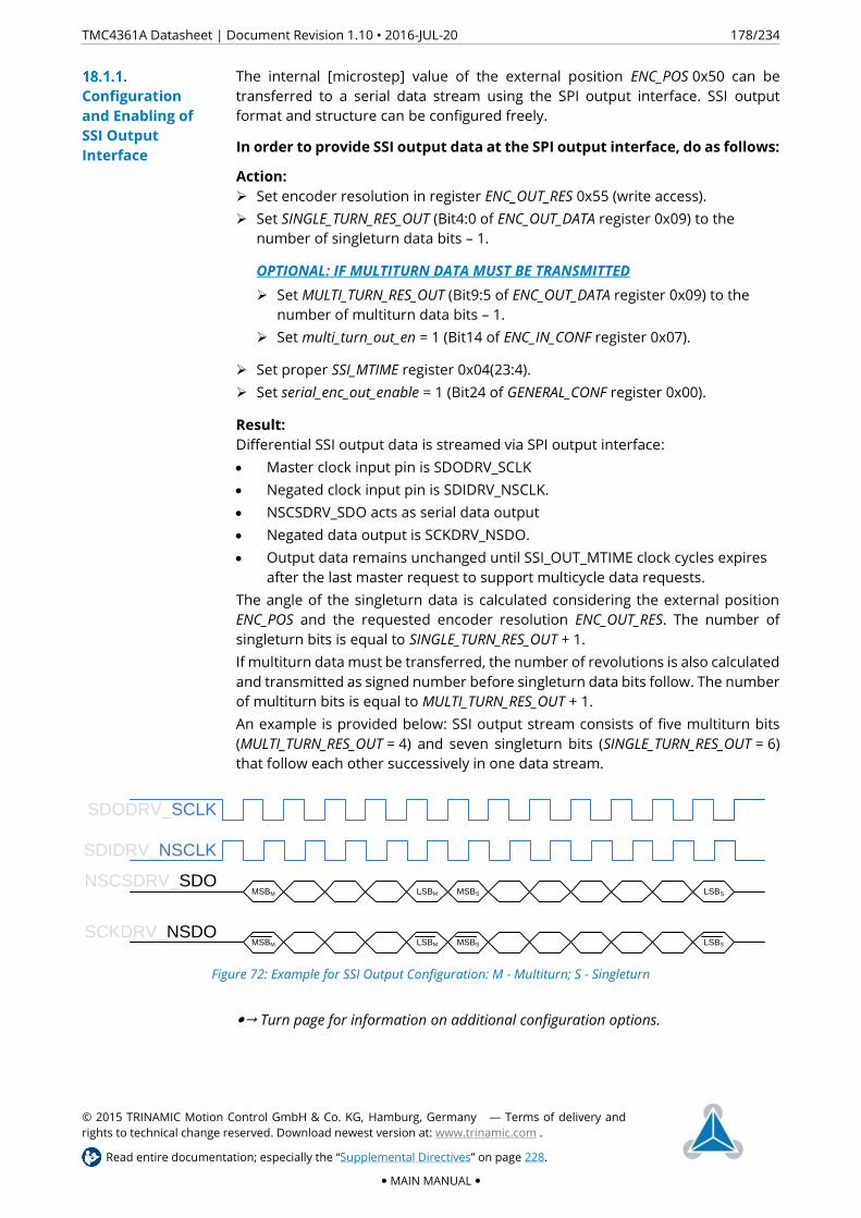
TMC4361A Datasheet | Document Revision 1.10 • 2016-JUL-20 178/234
© 2015 TRINAMIC Motion Control GmbH & Co. KG, Hamburg, Germany — Terms of delivery and
rights to technical change reserved. Download newest version at: www.trinamic.com .
Read entire documentation; especially the “Supplemental Directives” on page 228.
MAIN MANUAL
The internal [microstep] value of the external position ENC_POS 0x50 can be
transferred to a serial data stream using the SPI output interface. SSI output
format and structure can be configured freely.
In order to provide SSI output data at the SPI output interface, do as follows:
Action: Set encoder resolution in register ENC_OUT_RES 0x55 (write access).
Set SINGLE_TURN_RES_OUT (Bit4:0 of ENC_OUT_DATA register 0x09) to the
number of singleturn data bits – 1.
OPTIONAL: IF MULTITURN DATA MUST BE TRANSMITTED
Set MULTI_TURN_RES_OUT (Bit9:5 of ENC_OUT_DATA register 0x09) to the
number of multiturn data bits – 1.
Set multi_turn_out_en = 1 (Bit14 of ENC_IN_CONF register 0x07).
Set proper SSI_MTIME register 0x04(23:4).
Set serial_enc_out_enable = 1 (Bit24 of GENERAL_CONF register 0x00).
Result: Differential SSI output data is streamed via SPI output interface:
Master clock input pin is SDODRV_SCLK
Negated clock input pin is SDIDRV_NSCLK.
NSCSDRV_SDO acts as serial data output
Negated data output is SCKDRV_NSDO.
Output data remains unchanged until SSI_OUT_MTIME clock cycles expires
after the last master request to support multicycle data requests.
The angle of the singleturn data is calculated considering the external position
ENC_POS and the requested encoder resolution ENC_OUT_RES. The number of
singleturn bits is equal to SINGLE_TURN_RES_OUT + 1.
If multiturn data must be transferred, the number of revolutions is also calculated
and transmitted as signed number before singleturn data bits follow. The number
of multiturn bits is equal to MULTI_TURN_RES_OUT + 1.
An example is provided below: SSI output stream consists of five multiturn bits
(MULTI_TURN_RES_OUT = 4) and seven singleturn bits (SINGLE_TURN_RES_OUT = 6)
that follow each other successively in one data stream.
Figure 72: Example for SSI Output Configuration: M - Multiturn; S - Singleturn
Turn page for information on additional configuration options.
SDODRV_SCLK
MSBM LSBM MSBS LSBS
MSBM LSBM MSBS LSBS
SDIDRV_NSCLK
NSCSDRV_SDO
SCKDRV_NSDO
Configuration and Enabling of SSI Output Interface

TMC4361A Datasheet | Document Revision 1.10 • 2016-JUL-20 179/234
© 2015 TRINAMIC Motion Control GmbH & Co. KG, Hamburg, Germany — Terms of delivery and
rights to technical change reserved. Download newest version at: www.trinamic.com .
Read entire documentation; especially the “Supplemental Directives” on page 228.
MAIN MANUAL
Regular SSI operation makes use differential signals. Thus, TMC4361A expects
digital differential serial clock input signals.
In order to disable the digital differential output signals, do as follows:
Action: Set serial_enc_out_diff_disable = 1 (Bit25 of GENERAL_CONF register 0x00).
Result: Dedicated encoder signals are treated as single signals and every negated pin is
ignored.
TMC4361A is able to gray-encode SSI data automatically.
In order to enable gray-encoded SSI output data, do as follows:
Action: Set enc_out_gray =1 (Bit30 of ENC_IN_CONF register 0x07).
Result: Encoder data output is gray-encoded.
Disabling differential Encoder Output Signals
Gray-encoded SSI Output Data

TMC4361A Datasheet | Document Revision 1.10 • 2016-JUL-20 180/234
© 2015 TRINAMIC Motion Control GmbH & Co. KG, Hamburg, Germany — Terms of delivery and
rights to technical change reserved. Download newest version at: www.trinamic.com .
Read entire documentation; especially the “Supplemental Directives” on page 228.
MAIN MANUAL
TECHNICAL SPECIFICATIONS
19. Complete Register and Switches List
General Configuration Register GENERAL_CONF 0x00
GENERAL_CONF 0x00 (Default value: 0x00006020)
R/W Bit Val Remarks
RW
0
use_astart_and_vstart (only valid for S-shaped ramps)
0 Sets AACTUAL = AMAX or –AMAX at ramp start and in the case of VSTART ≠ 0.
1 Sets AACTUAL = ASTART or –ASTART at ramp start and in the case of VSTART ≠ 0.
1
direct_acc_val_en
0 Acceleration values are divided by CLK_FREQ.
1 Acceleration values are set directly as steps per clock cycle.
2
direct_bow_val_en
0 Bow values are calculated due to division by CLK_FREQ.
1 Bow values are set directly as steps per clock cycle.
3
step_inactive_pol
0 STPOUT = 1 indicates an active step.
1 STPOUT = 0 indicates an active step.
4
toggle_step
0 Only STPOUT transitions from inactive to active polarity indicate steps.
1 Every level change of STPOUT indicates a step.
5
pol_dir_out
0 DIROUT = 0 indicates negative direction.
1 DIROUT = 1 indicates negative direction.
7:6
sdin_mode
0 Internal step control (internal ramp generator will be used)
1 External step control via STPIN / DIRIN interface with high active steps at STPIN
2 External step control via STPIN / DIRIN interface with low active steps at STPIN
3 External step control via STPIN / DIRIN interface with toggling steps at STPIN
8
pol_dir_in
0 DIRIN = 0 indicates negative direction.
1 DIRIN = 1 indicates negative direction.
9
sd_indirect_control
0 STPIN/DIRIN input signals will manipulate internal steps at XACTUAL directly.
1 STPIN/DIRIN input signals will manipulate XTARGET register value, the internal
ramp generator is used.
Continued on next page.

TMC4361A Datasheet | Document Revision 1.10 • 2016-JUL-20 181/234
© 2015 TRINAMIC Motion Control GmbH & Co. KG, Hamburg, Germany — Terms of delivery and
rights to technical change reserved. Download newest version at: www.trinamic.com .
Read entire documentation; especially the “Supplemental Directives” on page 228.
MAIN MANUAL
GENERAL_CONF 0x00 (Default value: 0x00006020)
R/W Bit Val Remarks
RW
11:10
serial_enc_in_mode
0 An incremental encoder is connected to encoder interface.
1 An absolute SSI encoder is connected to encoder interface.
2 Reserved
3 An absolute SPI encoder is connected to encoder interface.
12
diff_enc_in_disab
0 Differential encoder interface inputs enabled.
1 Differential encoder interface inputs is disabled (automatically set for SPI
encoder).
14:13
stdby_clk_pin_assignment
0 Standby signal becomes forwarded with an active low level at STDBY_CLK
output.
1 Standby signal becomes forwarded with an active high level at STDBY_CLK
output.
2 STDBY_CLK passes ChopSync clock
(TMC23x, TMC24x stepper motor drivers only).
3 Internal clock is forwarded to STDBY_CLK output pin.
15
intr_pol
0 INTR=0 indicates an active interrupt.
1 INTR=1 indicates an active interrupt.
16
invert_pol_target_reached
0 TARGET_REACHED signal is set to 1 to indicate a target reached event.
1 TARGET_REACHED signal is set to 0 to indicate a target reached event.
17
clk_gating_en
0 Clock gating is disabled.
1 Internal clock gating is enabled.
18
clk_gating_stdby_en
0 No clock gating during standby phase.
1 Intenal clock gating during standby phase is enabled.
19
fs_en
0 Fullstep switchover is disabled.
1 SPI output forwards fullsteps, if |VACTUAL| > FS_VEL.
20
fs_sdout
0 No fullstep switchover for Step/Dir output is enabled.
1 Fullsteps are forwarded via Step/Dir output also if fullstep operation is active.
Continued on next page.

TMC4361A Datasheet | Document Revision 1.10 • 2016-JUL-20 182/234
© 2015 TRINAMIC Motion Control GmbH & Co. KG, Hamburg, Germany — Terms of delivery and
rights to technical change reserved. Download newest version at: www.trinamic.com .
Read entire documentation; especially the “Supplemental Directives” on page 228.
MAIN MANUAL
GENERAL_CONF 0x00 (Default value: 0x00006020)
R/W Bit Val Remarks
RW
22:21
dcstep_mode
0 dcStep is disabled.
1 dcStep signal generation will be selected automatically
2 dcStep with external STEP_READY signal generation (TMC2130).
3
dcStep with internal STEP_READY signal generation (TMC26x).
i TMC26x config: use const_toff-Chopper (CHM = 1); slow decay only (HSTRRT = 0); TST = 1 and SGT0=SGT1=1 (on_state_xy).
23
pwm_out_en
0 PWM output is disabled. Step/Dir output is enabled at STPOUT/DIROUT.
1 STPOUT/DIROUT output pins are used as PWM output (PWMA/PWMB).
24
serial_enc_out_enable
0 No encoder is connected to SPI output.
1 SPI output is used as SSI encoder interface to forward absolute SSI encoder data.
25
serial_enc_out_diff_disable
0 Differential serial encoder output is enabled.
1 Differential serial encoder output is disabled.
26
automatic_direct_sdin_switch_off
0 VACTUAL=0 & AACTUAL=0 after switching off direct external step control.
1 VACTUAL = VSTART and AACTUAL = ASTART after switching off direct external step
control.
27
circular_cnt_as_xlatch
0 The register value of X_LATCH is forwarded at register 0x36.
1 The register value of REV_CNT (#internal revolutions) is forwarded at register 0x36.
28
reverse_motor_dir
0 The direction of the internal SinLUT is regularly used.
1 The direction of internal SinLUT is reversed
29
intr_tr_pu_pd_en
0 INTR and TARGET_REACHED are outputs with strongly driven output values..
1 INTR and TARGET_REACHED are used as outputs with gated pull-up and/or
pull-down functionality.
30
intr_as_wired_and
0 INTR output function is used as Wired-Or in the case of intr_tr_pu_pd_en = 1.
1 INTR output function is used as Wired-And. in the case of intr_tr_pu_pd_en = 1.
31
tr_as_wired_and
0 TARGET_REACHED output function is used as Wired-Or in the case of
intr_tr_pu_pd_en = 1.
1 TARGET_REACHED output function is used as Wired-And in the case of
intr_tr_pu_pd_en = 1.
Table 65: General Configuration 0x00

TMC4361A Datasheet | Document Revision 1.10 • 2016-JUL-20 183/234
© 2015 TRINAMIC Motion Control GmbH & Co. KG, Hamburg, Germany — Terms of delivery and
rights to technical change reserved. Download newest version at: www.trinamic.com .
Read entire documentation; especially the “Supplemental Directives” on page 228.
MAIN MANUAL
Reference Switch Configuration Register REFERENCE_CONF 0x01
REFERENCE_CONF 0x01 (Default value: 0x00000000)
R/W Bit Val Remarks
RW
0
stop_left_en
0 STOPL signal processing disabled.
1 STOPL signal processing enabled.
1
stop_right_en
0 STOPR signal processing disabled.
1 STOPR signal processing enabled.
2
pol_stop_left
0 STOPL input signal is low active.
1 STOPL input signal is high active.
3
pol_stop_right
0 STOPR input signal is low active.
1 STOPR input signal is high active.
4
invert_stop_direction
0 STOPL/STOPR stops motor in negative/positive direction.
1 STOPL/STOPR stops motor in positive/negative direction.
5
soft_stop_en
0 Hard stop enabled. VACTUAL is immediately set to 0 on any external stop event.
1 Soft stop enabled. A linear velocity ramp is used for decreasing VACTUAL to v = 0.
6
virtual_left_limit_en
0 Position limit VIRT_STOP_LEFT disabled.
1 Position limit VIRT_STOP_LEFT enabled.
7
virtual_right_limit_en
0 Position limit VIRT_STOP_RIGHT disabled.
1 Position limit VIRT_STOP_RIGHT enabled.
9:8
virt_stop_mode
0 Reserved.
1 Hard stop: VACTUAL is set to 0 on a virtual stop event.
2 Soft stop is enabled with linear velocity ramp (from VACTUAL to v = 0).
3 Reserved.
10
latch_x_on_inactive_l
0 No latch of XACTUAL if STOPL becomes inactive.
1 X_LATCH = XACTUAL is stored in the case STOPL becomes inactive.
11
latch_x_on_active_l
0 No latch of XACTUAL if STOPL becomes active.
1 X_LATCH = XACTUAL is stored in the case STOPL becomes active.
Continued on next page.

TMC4361A Datasheet | Document Revision 1.10 • 2016-JUL-20 184/234
© 2015 TRINAMIC Motion Control GmbH & Co. KG, Hamburg, Germany — Terms of delivery and
rights to technical change reserved. Download newest version at: www.trinamic.com .
Read entire documentation; especially the “Supplemental Directives” on page 228.
MAIN MANUAL
REFERENCE_CONF 0x01 (Default value: 0x00000000)
R/W Bit Val Remarks
RW
12
latch_x_on_inactive_r
0 No latch of XACTUAL if STOPR becomes inactive.
1 X_LATCH = XACTUAL is stored in the case STOPL becomes inactive.
13
latch_x_on_active_r
0 No latch of XACTUAL if STOPR becomes active.
1 X_LATCH = XACTUAL is stored in the case STOPL becomes active.
14
stop_left_is_home
0 STOPL input signal is not also the HOME position.
1 STOPL input signal is also the HOME position.
15
stop_right_is_home
0 STOPR input signal is not lso the HOME position.
1 STOPR input signal is also the HOME position.
19:16
home_event
0 Next active N event of connected ABN encoder signal indicates HOME position.
2 HOME_REF = 1 indicates an active home event
X_HOME is located at the rising edge of the active range.
3 HOME_REF = 0 indicates negative region/position from the home position.
4 HOME_REF = 1 indicates an active home event
X_HOME is located at the falling edge of the active range.
6 HOME_REF = 1 indicates an active home event
X_HOME is located in the middle of the active range.
9 HOME_REF = 0 indicates an active home event
X_HOME is located in the middle of the active range.
11 HOME_REF = 0 indicates an active home event
X_HOME is located at the rising edge of the active range.
12 HOME_REF = 1 indicates negative region/position from the home position.
13 HOME_REF = 0 indicates an active home event
X_HOME is located at the falling edge of the active range.
20
start_home_tracking
0 No storage to X_HOME by passing home position.
1
Storage of XACTUAL as X_HOME at next regular home event.
An XLATCH_DONE event is released.
In case the event is cleared, start_home_tracking is reset automatically.
21
clr_pos_at_target
0 Ramp stops at XTARGET if positioning mode is active.
1 Set XACTUAL = 0 after XTARGET has been reached.
The next ramp starts immediately.
22
circular_movement_en
0 Range of XACTUAL is not limited: -231 ≤ XACTUAL ≤ 231-1
1 Range of XACTUAL is limited by X_RANGE: -X_RANGE ≤ XACTUAL ≤ X_RANGE - 1
Continued on next page.

TMC4361A Datasheet | Document Revision 1.10 • 2016-JUL-20 185/234
© 2015 TRINAMIC Motion Control GmbH & Co. KG, Hamburg, Germany — Terms of delivery and
rights to technical change reserved. Download newest version at: www.trinamic.com .
Read entire documentation; especially the “Supplemental Directives” on page 228.
MAIN MANUAL
REFERENCE_CONF 0x01 (Default value: 0x00000000)
R/W Bit Val Remarks
RW
24:23
pos_comp_output
0 TARGET_REACHED is set active on TARGET_REACHED_Flag.
1 TARGET_REACHED is set active on VELOCITY_REACHED_Flag.
2 TARGET_REACHED is set active on ENC_FAIL flag.
3 TARGET_REACHED triggers on POSCOMP_REACHED_Flag.
25
pos_comp_source
0 POS_COMP is compared to internal position XACTUAL.
1 POS_COMP is compared with external position ENC_POS.
26
stop_on_stall
0 SPI and S/D output interface remain active in case of an stall event.
1 SPI and S/D output interface stops motion in case of an stall event (hard stop).
27
drv_after_stall
0 No further motion in case of an active stop-on-stall event.
1 Motion is possible in case of an active stop-on-stall event and after the stop-on-
stall event is reset.
29:28
modified_pos_compare:
POS_COMP_REACHED_F / event is based on comparison
between XACTUAL resp. ENC_POS and
0 POS_COMP
1 X_HOME
2 X_LATCH resp. ENC_LATCH
3 REV_CNT
30
automatic_cover
0 SPI output interface will not transfer automatically any cover datagram.
1 SPI output interface sends automatically cover datagrams when VACTUAL crosses
SPI_SWITCH_VEL.
31
circular_enc_en
0 Range of ENC_POS is not limited: -231 ≤ ENC_POS ≤ 231-1
1 Range of ENC_POS is limited by X_RANGE: -X_RANGE ≤ ENC_POS ≤ X_RANGE –1
Table 66: Reference Switch Configuration 0x01

TMC4361A Datasheet | Document Revision 1.10 • 2016-JUL-20 186/234
© 2015 TRINAMIC Motion Control GmbH & Co. KG, Hamburg, Germany — Terms of delivery and
rights to technical change reserved. Download newest version at: www.trinamic.com .
Read entire documentation; especially the “Supplemental Directives” on page 228.
MAIN MANUAL
Start Switch Configuration Register START_CONF 0x02
START_CONF 0x02 (Default value: 0x00000000)
R/W Bit Val Remarks
RW
4:0
start_en
xxxx1 Alteration of XTARGET value requires distinct start signal.
xxx1x Alteration of VMAX value requires distinct start signal.
xx1xx Alteration of RAMPMODE value requires distinct start signal.
x1xxx Alteration of GEAR_RATIO value requires distinct start signal.
1xxxx Shadow Register Feature Set is enabled.
8:5
trigger_events
0000 Timing feature set is disabled because start signal generation is disabled.
xxx0 START pin is assigned as output.
xxx1 External start signal is enabled as timer trigger. START pin is assigned as input.
xx1x TARGET_REACHED event is assigned as start signal trigger.
x1xx VELOCITY_REACHED event is assigned as start signal trigger.
1xxx POSCOMP_REACHED event is assigned as start signal trigger.
9
pol_start_signal
0 START pin is low active (input resp. output).
1 START pin is high active (input resp. output).
10
immediate_start_in
0 Active START input signal starts internal start timer.
1 Active START input signal is executed immediately.
11
busy_state_en
0 START pin is only assigned as input or output.
1 Busy start state is enabled. START pin is assigned as input with a weakly driven
active start polarity or as output with a strongly driven inactive start polarity.
15:12
pipeline_en
0000 No pipelining is active.
xxx1 X_TARGET is considered for pipelining.
xx1x POS_COMP is considered for pipelining.
x1xx GEAR_RATIO is considered for pipelining.
1xxx GENERAL_CONF is considered for pipelining.
17:16
shadow_option
0 Single-level shadow registers for 13 relevant ramp parameters.
1 Double-stage shadow registers for S-shaped ramps.
2 Double-stage shadow registers for trapezoidal ramps (excl. VSTOP).
3 Double-stage shadow registers for trapezoidal ramps (excl. VSTART).
Continued on next page.

TMC4361A Datasheet | Document Revision 1.10 • 2016-JUL-20 187/234
© 2015 TRINAMIC Motion Control GmbH & Co. KG, Hamburg, Germany — Terms of delivery and
rights to technical change reserved. Download newest version at: www.trinamic.com .
Read entire documentation; especially the “Supplemental Directives” on page 228.
MAIN MANUAL
START_CONF 0x02 (Default value: 0x00000000)
R/W Bit Val Remarks
RW
18
cyclic_shadow_regs
0 Current ramp parameters are not written back to the shadow register.
1 Current ramp parameters are written back to the appropriate shadow register.
19 Reserved. Set to 0.
23:20
SHADOW_MISS_CNT
U Number of unused start internal start signals between two consecutive
shadow register transfers.
31:24
XPIPE_REWRITE_REG
Current assigned pipeline registers – START_CONF(15:12) – are written back to
X_PIPEx in the case of an internal start signal generation and if assigned in this
register with a ‘1’:
XPIPE_REWRITE_REG(0) à X_PIPE0
XPIPE_REWRITE_REG(1) à X_PIPE1
XPIPE_REWRITE_REG(2) à X_PIPE2
XPIPE_REWRITE_REG(3) à X_PIPE3
XPIPE_REWRITE_REG(4) à X_PIPE4
XPIPE_REWRITE_REG(5) à X_PIPE5
XPIPE_REWRITE_REG(6) à X_PIPE6
XPIPE_REWRITE_REG(7) à X_PIPE7
Ex.:
START_CONF(15:12) = b’0011.
START_CONF(31:24) = b’01000010.
If an internal start signal is generated, the value of X_TARGET is written back to
X_PIPE1, whereas the value of POS_COMP is written back to X_PIPE6.
Table 67: Start Switch Configuration START_CONF 0x02

TMC4361A Datasheet | Document Revision 1.10 • 2016-JUL-20 188/234
© 2015 TRINAMIC Motion Control GmbH & Co. KG, Hamburg, Germany — Terms of delivery and
rights to technical change reserved. Download newest version at: www.trinamic.com .
Read entire documentation; especially the “Supplemental Directives” on page 228.
MAIN MANUAL
Input Filter Configuration Register INPUT_FILT_CONF 0x03
INPUT_FILT_CONF 0x03 (Default value: 0x00000000)
R/W Bit Val Remarks
RW
2:0
SR_ENC_IN
U Input sample rate = fclk / 2SR_ENC_IN for the following pins:
A_SCLK, ANEG_NSCLK, B_SDI, BNEG_NSDI, N, NNEG
3 Reserved. Set to 0.
6:4
FILT_L_ENC_IN
U
Filter length for these pins: A_SCLK, ANEG_NSCLK, B_SDI, BNEG_NSDI, N, NNEG.
Number of sample input bits that must have equal voltage levels to provide a
valid input bit.
7
SD_FILT0
0 S/D input pins (STPIN/DIRIN) are not assigned to the ENC_IN input filter group.
1 S/D input pins (STPIN/DIRIN) are also assigned to the ENC_IN input filter group.
10:8 SR_REF
U Input sample rate = fclk / 2REF for the following pins: STOPL, HOME_REF, STOPL
11 Reserved. Set to 0.
14:12
FILT_L_ENC_IN
U Filter length for the following pins: STOPL, HOME_REF, STOPL. Number of
sample input bits that must have equal voltage levels to provide a valid input bit.
15
SD_FILT1
0 S/D input pins (STPIN/DIRIN) are not assigned to the REF input filter group.
1 S/D input pins (STPIN/DIRIN) are also assigned to the REF input filter group.
18:16 SR_S
U Input sample rate = fclk / 2S for the START pin.
19 Reserved. Set to 0.
22:20
FILT_L_S
U Filter length for the START pin. Number of sample input bits that must have
equal voltage levels to provide a valid input bit.
23
SD_FILT2
0 S/D input pins (STPIN/DIRIN) are not assigned to the S input filter group.
1 S/D input pins (STPIN/DIRIN) are also assigned to the S input filter group.
26:24 SR_ENC_OUT
U Input sample rate = fclk / 2SR_ENC_OUT for these pins: SDODRV_SCLK, SDIDRV_NSCLK
27 Reserved. Set to 0.
30:28
FILT_L_ENC_OUT
U Filter length for the following pins: SDODRV_SCLK, SDIDRV_NSCLK. Number of
sample input bits that must have equal voltage levels to provide a valid input bit.
31
SD_FILT3
0 S/D input pins (STPIN/DIRIN) are not assigned to the ENC_OUT input filter group.
1 S/D input pins (STPIN/DIRIN) are assigned to the ENC_OUT input filter group.
Table 68: Input Filter Configuration Register INPUT_FILT_CONF 0x03

TMC4361A Datasheet | Document Revision 1.10 • 2016-JUL-20 189/234
© 2015 TRINAMIC Motion Control GmbH & Co. KG, Hamburg, Germany — Terms of delivery and
rights to technical change reserved. Download newest version at: www.trinamic.com .
Read entire documentation; especially the “Supplemental Directives” on page 228.
MAIN MANUAL
SPI Output Configuration Register SPI_OUT_CONF 0x04
SPI_OUT_CONF 0x04 (Default value: 0x00000000)
R/W Bit Val Remarks
RW
3:0
spi_output_format
0 SPI output interface is off.
1
SPI output interface is connected with a SPI-DAC. SPI output values are mapped
to full amplitude:
Current=0 à VCC/2
Current=-max à 0
Current=max à VCC
2
SPI output interface is connected with a SPI-DAC. SPI output values are absolute
values. Phase of coilA is forwarded via STPOUT, whereas phase of coilB is
forwarded via DIROUT. Phase bit = 0:positive value.
3
SPI output interface is connected with a SPI-DAC. SPI output values are absolute
values. Phase of coilA is forwarded via STPOUT, whereas phase of coilB is
forwarded via DIROUT. Phase bit = 0: negative value.
4 The actual unsigned scaling factor is forwarded via SPI output interface.
5 Both actual signed current values CURRENTA and CURRENTB are forwarded in
one datagram via SPI output interface.
6 SPI output interface is connected with a SPI-DAC. The actual unsigned scaling factor is merged with DAC_ADDR_A value to an output datagram.
8 SPI output interface is connected with a TMC23x stepper motor driver.
9 SPI output interface is connected with a TMC24x stepper motor driver.
10 SPI output interface is connected with a TMC26x/389 stepper motor driver.
Configuration and current data are transferred to the stepper motor driver.
11
SPI output interface is connected with a TMC26x stepper motor driver. Only
configuration data is transferred to the stepper motor driver. S/D output
interface provides steps.
12
SPI output interface is connected with a TMC2130 stepper motor driver. Only
configuration data is transferred to the stepper motor driver. S/D output
interface provides steps.
13 SPI output interface is connected with a TMC2130 stepper motor driver.
Configuration and current data are transferred to the stepper motor driver.
15 Only cover datagrams are transferred via SPI output interface.
19:13
COVER_DATA_LENGTH
U
Number of bits for the complete datagram length. Maximum value = 64
Set to 0 in case a TMC stepper motor driver is selected. The datagram length is
then selected automatically.
23:20 SPI_OUT_LOW_TIME
U Number of clock cycles the SPI output clock remains at low level.
27:24 SPI_OUT_HIGH_TIME
U Number of clock cycles the SPI output clock remains at high level.
31:28
SPI_OUT_BLOCK_TIME
U Number of clock cycles the NSCSDRV output remains high (inactive) after a SPI
output transmission.
Continued on next page.

TMC4361A Datasheet | Document Revision 1.10 • 2016-JUL-20 190/234
© 2015 TRINAMIC Motion Control GmbH & Co. KG, Hamburg, Germany — Terms of delivery and
rights to technical change reserved. Download newest version at: www.trinamic.com .
Read entire documentation; especially the “Supplemental Directives” on page 228.
MAIN MANUAL
SPI_OUT_CONF 0x04 (Default value: 0x00000000)
R/W Bit Val Remarks
RW
5:4
mixed_decay (TMC23x/24x only)
0 Both mixed decay bits are always off.
1 Mixed decay bits are on during falling ramps until reaching a current value of 0.
2 Mixed decay bits are always on, except during standstill.
3 Mixed decay bits are always on.
6
stdby_on_stall_for_24x (TMC24x only)
0 No standby datagram is sent.
1 In case of a Stop-on-Stall event, a standby datagram is sent to the TMC24x.
7
stall_flag_instead_of_uv_en (TMC24x only)
0 Undervoltage flag of TMC24x is mapped at STATUS(24).
1 Calculated stall status of TMC24x is forwarded at STATUS(24).
10:8
STALL_LOAD_LIMIT (TMC24x only)
U A stall is detected if the stall limit value STALL_LOAD_LIMIT is higher than the
combination of the load bits (LD2&LD1&LD0).
11
pwm_phase_shft_en (TMC24x only)
0 No phase shift during PWM mode.
1
During PWM mode, the internal SinLUT microstep position MSCNT is shifted to
MS_OFFSET microsteps. Consequently, the sine/cosine values have a phase shift
of (MS_OFFSET / 1024 ∙ 360°)
12
double_freq_at_stdby (TMC23x/24x only)
0 ChopSync frequency remains stable during standby.
1 CHOP_SYNC_DIV is halfed during standby.
4
three_phase_stepper_en (TMC389 only)
0 A 2-phase stepper motor driver is connected to the SPI output (TMC26x).
1 A 3-phase stepper motor driver is connected to the SPI output (TMC389).
5
scale_val_transfer_en (TMC26x/2130 in SD mode only)
0 No transfer of scale values.
1 Transmission of current scale values to the appropriate driver registers.
6
disable_polling (TMC26x/2130 in SD mode only)
0 Permanent transfer of polling datagrams to check driver status.
1 No transfer of polling datagrams.
7
autorepeat_cover_en (TMC26x/2130 only)
0 No automatic continuous streaming of cover datagrams.
1 Enabling of automatic continuous streaming of cover datagrams.
11:8
POLL_BLOCK_EXP (TMC26x in SD mode only, TMC2130 only)
U Multiplier for calculating the time interval between two consecutive polling
datagrams: tPOLL = 2^POLL_BLOCK_EXP ∙ SPI_OUT_BLOCK_TIME / fCLK
12
cover_done_only_for_cover (TMC26x/2130 only)
0 COVER_DONE event is set for every datagram that is sent to the motor driver.
1 COVER_DONE event is only set for cover datagrams sent to the motor driver.

TMC4361A Datasheet | Document Revision 1.10 • 2016-JUL-20 191/234
© 2015 TRINAMIC Motion Control GmbH & Co. KG, Hamburg, Germany — Terms of delivery and
rights to technical change reserved. Download newest version at: www.trinamic.com .
Read entire documentation; especially the “Supplemental Directives” on page 228.
MAIN MANUAL
SPI_OUT_CONF 0x04 (Default value: 0x00000000)
R/W Bit Val Remarks
RW
4
sck_low_before_csn (No TMC driver)
0 NSCSDRV_SDO is tied low before SCKDRV_NSDO to initiate a new data transfer.
1 SCKDRV_NSDO is tied low before NSCSDRV_SDO to initiate a new data transfer.
5
new_out_bit_at_rise (No TMC driver)
0 New value bit at SDODRV_SCLK is assigned at falling edge of SCKDRV_NSDO.
1 New value bit at SDODRV_SCLK is assigned at rising edge of SCKDRV_NSDO.
11:7 DAC_CMD_LENGTH (SPI-DAC only)
U Number of bits for command address.
12 Reserved. Set to 0.
23:4
SSI_OUT_MTIME (Serial encoder output only)
U Monoflop time for SSI output interface: Delay time [clock cycles] during which
the absolute encoder data remain stable after the last master request.
Table 69: SPI Output Configuration Register SPI_OUT_CONF 0x04

TMC4361A Datasheet | Document Revision 1.10 • 2016-JUL-20 192/234
© 2015 TRINAMIC Motion Control GmbH & Co. KG, Hamburg, Germany — Terms of delivery and
rights to technical change reserved. Download newest version at: www.trinamic.com .
Read entire documentation; especially the “Supplemental Directives” on page 228.
MAIN MANUAL
Current Scaling Configuration Register CURRENT_CONF 0x05
CURRENT_CONF 0x05 (Default: 0x00000000)
R/W Bit Val Remarks
RW
0
hold_current_scale_en
0 No hold current scaling during standstill phase.
1 Hold current scaling during standstill phase.
1
drive_current_scale_en
0 No drive current scaling during motion.
1 Drive current scaling during motion.
2
boost_current_on_acc_en
0 No boost current scaling for deceleration ramps.
1 Boost current scaling if RAMP_STATE = b’01 (acceleration slopes).
3
boost_current_on_dec_en
0 No boost current scaling for deceleration ramps.
1 Boost current scaling if RAMP_STATE = b’10 (deceleration slopes).
4
boost_current_after_start_en
0 No boost current at ramp start.
1 Temporary boost current if VACTUAL = 0 and new ramp starts.
5
sec_drive_current_scale_en
0 One drive current value for the whole motion ramp.
1 Second drive current scaling for VACTUAL > VDRV_SCALE_LIMIT.
6
freewheeling_en
0 No freewheeling.
1 Freewheeling after standby phase.
7
closed_loop_scale_en
0 No closed-loop current scaling.
1 Closed-loop current scaling – CURRENT_CONF(6:0) = 0 is set automatically
Turn off for closed-loop calibration with maximum current!
8
pwm_scale_en
0 PWM scaling is disabled.
1 PWM scaling is enabled.
15:9 Reserved. Set to 0x00.
31:16
PWM_AMPL
U
PWM amplitude during Voltage PWM mode at VACTUAL = 0.
i Maximum duty cycle = (0.5 + (PWM_AMPL + 1) / 217) Minimum duty cycle = (0.5 – (PWM_AMPL + 1) / 217) PWM_AMPL = 216 – 1 at VACTUAL = PWM_VMAX.
Table 70: Current Scale Configuration (0x05)

TMC4361A Datasheet | Document Revision 1.10 • 2016-JUL-20 193/234
© 2015 TRINAMIC Motion Control GmbH & Co. KG, Hamburg, Germany — Terms of delivery and
rights to technical change reserved. Download newest version at: www.trinamic.com .
Read entire documentation; especially the “Supplemental Directives” on page 228.
MAIN MANUAL
Current Scale Values Register SCALE_VALUES 0x06
SCALE_VALUES 0x06 (Default: 0xFFFFFFFF)
R/W Bit Val Scaling Value Name Remarks
RW
7:0 U BOOST_SCALE_VAL Open-loop boost scaling value.
CL_IMIN Closed-loop minimum scaling value.
15:8 U DRV1_SCALE_VAL Open-loop first drive scaling value.
CL_IMAX Closed-loop maximum scaling value.
23:16 U
DRV2_SCALE_VAL Open-loop second drive scaling value.
CL_START_UP |ENC_POS_DEV| value at which closed-loop scaling
increases the current scaling value above CL_IMIN.
31:24 U
HOLD_SCALE_VAL Open-loop standby scaling value.
CL_START_DOWN
|ENC_POS_DEV| value at which closed-loop scaling
decreases the current scaling value below CL_IMAX.
i Recommended: Set to 0 to automatically assign to CL_BETA.
Table 71: Current Scale Values (0x06)
NOTE:
BOOST_SCALE_VAL, DRV1/DRV2_SCALE_VAL, HOLD_SCALE_VAL, CL_IMIN, CL_IMAX.
Real scaling value = (x+1) / 32 if spi_output_format = b’1011 or b’1100.
= (x+1) / 256 any other spi_output_format setting.

TMC4361A Datasheet | Document Revision 1.10 • 2016-JUL-20 194/234
© 2015 TRINAMIC Motion Control GmbH & Co. KG, Hamburg, Germany — Terms of delivery and
rights to technical change reserved. Download newest version at: www.trinamic.com .
Read entire documentation; especially the “Supplemental Directives” on page 228.
MAIN MANUAL
Encoder Signal Configuration (0x07)
ENC_IN_CONF 0x07 (Default 0x00000400)
R/W Bit Val Description
RW
0
enc_sel_decimal
0 Encoder constant represents a binary number.
1 Encoder constant represents a decimal number (for ABN only).
1
clear_on_n
0 ENC_POS is not set to ENC_RESET_VAL.
1
ENC_POS is set to ENC_RESET_VAL
on every N event in case clr_latch_cont_on_n=1, or
on the next N event in case clr_latch_once_on_n=1.
Do NOT use during closed-loop operation.
2
clr_latch_cont_on_n
0 Value of ENC_POS is not cleared and/or latched on every N event.
1 Value of ENC_POS is cleared and/or latched on every N event.
3
clr_latch_once_on_n
0 Value of ENC_POS is not cleared and/or latched on the next N event.
1 Value of ENC_POS is cleared and/or latched on the next N event.
i This bit is set to 0 after latching/clearing once.
4
pol_n
0 Active polarity for N event is low active.
1 Active polarity for N event is high active.
6:5
n_chan_sensitivity
0 N event is active as long as N equals active N event polarity.
1 N event triggers when N switches to active N event polarity.
2 N event triggers when N switches to inactive N event polarity.
3 N event triggers when N switches to in-/active N event polarity (both slopes).
7
pol_a_for_n
0 A polarity has to be low for a valid N event.
1 A polarity has to be high for a valid N event.
8
pol_b_for_n
0 B polarity has to be low for valid N event
B polarity has to be high for valid N event 1
9
ignore_ab
0 TMC4361A considers A and B polarities for valid N event.
1 Polarities of A and B signals for a valid N event are ignored.
Continued on next page.

TMC4361A Datasheet | Document Revision 1.10 • 2016-JUL-20 195/234
© 2015 TRINAMIC Motion Control GmbH & Co. KG, Hamburg, Germany — Terms of delivery and
rights to technical change reserved. Download newest version at: www.trinamic.com .
Read entire documentation; especially the “Supplemental Directives” on page 228.
MAIN MANUAL
ENC_IN_CONF 0x07 (Default 0x00000400)
R/W Bit Val Description
RW
10
latch_enc_on_n
0 ENC_POS is not latched.
1
ENC_POS is latched to ENC_LATCH
on every N event in case clr_latch_cont_on_n=1, or
on the next N event in case clr_latch_once_on_n=1.
11
latch_x_on_n
0 XACTUAL is not latched.
1
XACTUAL is latched to X_LATCH
on every N event in case clr_latch_cont_on_n=1, or
on the next N event in case clr_latch_once_on_n=1.
12
multi_turn_in_en (Absolute encoder only)
0 Connected serial encoder transmits singleturn values.
1 Connected serial encoder input transmits singleturn and multiturn values.
13
multi_turn_in_signed (Absolute encoder only)
0 Multiturn values from serial encoder input are unsigned numbers.
1 Multiturn values from serial encoder input are signed numbers.
14
multi_turn_out_en (Serial encoder output only)
0 Serial encoder output transmits singleturn values.
1 Serial encoder output transmits singleturn and multiturn values.
15
use_usteps_instead_of_xrange
0 X_RANGE is valid in case circular motion is also enabled for encoders.
1 USTEPS_PER_REV is valid in case circular motion is also enabled for encoders.
16
calc_multi_turn_behav (Absolute encoder only)
0 No multiturn calculation.
1 TMC4361A calculates internally multiturn data for singleturn encoder data.
17
ssi_multi_cycle_data (Absolute encoder only)
0 Every SSI value request is executed once.
1 Every SSI value request is executed twice.
18
ssi_gray_code_en (Absolute encoder only)
0 SSI input data is binary-coded.
1 SSI input data is gray-coded.
19
left_aligned_data (Absolute encoder only)
0 Serial input data is aligned right (first flags, then data).
1 Serial input data is aligned left (first data, then flags).
Continued on next page.
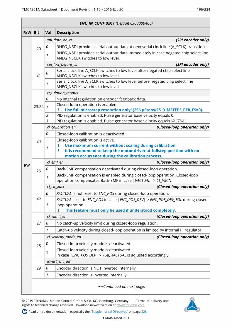
TMC4361A Datasheet | Document Revision 1.10 • 2016-JUL-20 196/234
© 2015 TRINAMIC Motion Control GmbH & Co. KG, Hamburg, Germany — Terms of delivery and
rights to technical change reserved. Download newest version at: www.trinamic.com .
Read entire documentation; especially the “Supplemental Directives” on page 228.
MAIN MANUAL
ENC_IN_CONF 0x07 (Default 0x00000400)
R/W Bit Val Description
RW
20
spi_data_on_cs (SPI encoder only)
0 BNEG_NSDI provides serial output data at next serial clock line (A_SCLK) transition.
1 BNEG_NSDI provides serial output data immediately in case negated chip select line
ANEG_NSCLK switches to low level.
21
spi_low_before_cs (SPI encoder only)
0 Serial clock line A_SCLK switches to low level after negated chip select line
ANEG_NSCLK switches to low level.
1 Serial clock line A_SCLK switches to low level before negated chip select line
ANEG_NSCLK switches to low level.
23:22
regulation_modus
0 No internal regulation on encoder feedback data.
1 Closed-loop operation is enabled.
Use full microstep resolution only! (256 µSteps/FS à MSTEPS_PER_FS=0). 2 PID regulation is enabled. Pulse generator base velocity equals 0.
3 PID regulation is enabled. Pulse generator base velocity equals VACTUAL.
24
cl_calibration_en (Closed-loop operation only)
0 Closed-loop calibration is deactivated.
1
Closed-loop calibration is active.
Use maximum current without scaling during calibration. It is recommend to keep the motor driver at fullstep position with no
motion occurrence during the calibration process.
25
cl_emf_en (Closed-loop operation only)
0 Back-EMF compensation deactivated during closed-loop operation.
1 Back-EMF compensation is enabled during closed-loop operation. Closed-loop
operation compensates Back-EMF in case |VACTUAL| > CL_VMIN.
26
cl_clr_xact (Closed-loop operation only)
0 XACTUAL is not reset to ENC_POS during closed-loop operation.
1
XACTUAL is set to ENC_POS in case |ENC_POS_DEV| > ENC_POS_DEV_TOL during closed-
loop operation.
This feature must only be used if understood completely.
27
cl_vlimit_en (Closed-loop operation only)
0 No catch-up velocity limit during closed-loop regulation.
1 Catch-up velocity during closed-loop operation is limited by internal PI regulator.
28
cl_velocity_mode_en (Closed-loop operation only)
0 Closed-loop velocity mode is deactivated.
1 Closed-loop velocity mode is deactivated.
In case |ENC_POS_DEV| > 768, XACTUAL is adjusted accordingly.
29
invert_enc_dir
0 Encoder direction is NOT inverted internally.
1 Encoder direction is inverted internally.
Continued on next page.

TMC4361A Datasheet | Document Revision 1.10 • 2016-JUL-20 197/234
© 2015 TRINAMIC Motion Control GmbH & Co. KG, Hamburg, Germany — Terms of delivery and
rights to technical change reserved. Download newest version at: www.trinamic.com .
Read entire documentation; especially the “Supplemental Directives” on page 228.
MAIN MANUAL
ENC_IN_CONF 0x07 (Default 0x00000400)
R/W Bit Val Description
RW
30
enc_out_gray (Serial encoder output only)
0 SSI output data is binary-encoded.
1 SSI output data is gray-encoded.
31
no_enc_vel_preproc (Incremental ABN encoder)
0 AB signal is preprocessed for internal encoder velocity calculation.
1
No AB signal preprocessing.
It is recommend to maintain AB preprocessing in order to filter encoder resonances.
serial_enc_variation_limit (Absolute encoder)
0 No variation limit on absolute encoder data.
1
Two consecutive serial encoder values must no deviate from specified limit to be
valid.
In case |ENC_POSX – ENC_POSX-1| > 1/8 · SER_ENC_VARIATION · ENC_IN_RES, ENC_POSX is
not valid and is not assigned to ENC_POS.
Table 72: Encoder Signal Configuration ENC_IN_CONF (0x07)
Serial Encoder Data Input Configuration (0x08)
ENC_IN_DATA 0x08 (Default: 0x00000000)
R/W Bit Val Remarks
RW
4:0
SINGLE_TURN_RES (Default: 0x00)
U Number of angle data bits within one revolution = SINGLE_TURN_RES + 1.
Set SINGLE_TURN_RES < 31.
9:5 MULTI_TURN_RES (Default: 0x00)
U Number of data bits for revolution count = MULTI_TURN_RES + 1
11:10 STATUS_BIT_CNT (Default: 0x0)
U Number of status data bits
15:12 Reserved. Set to 0x0.
23:16 SERIAL_ADDR_BITS (Default: 0x00) (SPI encoder only)
U Number of address bits within one SPI datagram for SPI encoder configuration
31:24 SERIAL_DATA_BITS (Default: 0x00) (SPI encoder only)
U Number of data bits within one SPI datagram for SPI encoder configuration
Table 73: Serial Encoder Data Input Configuration ENC_IN_DATA (0x08)

TMC4361A Datasheet | Document Revision 1.10 • 2016-JUL-20 198/234
© 2015 TRINAMIC Motion Control GmbH & Co. KG, Hamburg, Germany — Terms of delivery and
rights to technical change reserved. Download newest version at: www.trinamic.com .
Read entire documentation; especially the “Supplemental Directives” on page 228.
MAIN MANUAL
Serial Encoder Data Output Configuration (0x09)
ENC_OUT_DATA 0x09 (Default: 0x00000000)
R/W Bit Val Remarks
RW
4:0 SINGLE_TURN_RES_OUT (Default: 0x00)
U Number of angle data bits within one revolution = SINGLE_TURN_RES_OUT + 1
9:5 MULTI_TURN_RES_OUT (Default: 0x00)
U Number of data bits for revolution count = MULTI_TURN_RES_OUT + 1
31:12 Reserved. Set to 0x00000.
Table 74: Serial Encoder Data Output Configuration ENC_OUT_DATA (0x09)

TMC4361A Datasheet | Document Revision 1.10 • 2016-JUL-20 199/234
© 2015 TRINAMIC Motion Control GmbH & Co. KG, Hamburg, Germany — Terms of delivery and
rights to technical change reserved. Download newest version at: www.trinamic.com .
Read entire documentation; especially the “Supplemental Directives” on page 228.
MAIN MANUAL
Motor Driver Settings Register STEP_CONF 0x0A
STEP_CONF 0x0A (Default: 0x00FB0C80)
R/W Bit Val Remarks
RW
3:0
MSTEP_PER_FS (Default: 0x0)
0
Highest microsteps resolution: 256 microsteps per fullstep.
i Set to 256 for closed-loop operation. i When using a Step/Dir driver, it must be capable of a 256 resolution
via Step/Dir input for best performance (but lower resolution Step/Dir drivers can be used as well).
1 128 microsteps per fullstep.
2 64 microsteps per fullstep.
3 32 microsteps per fullstep.
4 16 microsteps per fullstep.
5 8 microsteps per fullstep.
6 4 microsteps per fullstep.
7 Halfsteps: 2 microsteps per fullstep.
8 Full steps (maximum possible setting)
15:4 FS_PER_REV (Default: 0x0C8)
U Fullsteps per motor axis revolution
23:16
MSTATUS_SELECTION (Default: 0xFB)
Selection of motor driver status bits for SPI response datagrams:
ORed with Motor Driver Status Register Set (7:0):
if set here and a particular flag is set from the motor stepper driver, an event will
be generated at EVENTS(30)
31:24 Reserved. Set to 0x00.
Table 75: Motor Driver Settings (0x0A)

TMC4361A Datasheet | Document Revision 1.10 • 2016-JUL-20 200/234
© 2015 TRINAMIC Motion Control GmbH & Co. KG, Hamburg, Germany — Terms of delivery and
rights to technical change reserved. Download newest version at: www.trinamic.com .
Read entire documentation; especially the “Supplemental Directives” on page 228.
MAIN MANUAL
Event Selection Registers 0x0B..0X0D
Event Selection Registers
R/W Addr Bit Remarks
RW
0x0B
SPI_STATUS_SELECTION (Default: 0x82029805)
31:0
Events selection for SPI datagrams:
Event bits of EVENTS register 0x0E that are selected (=1) in this register are
forwarded to the eight status bits that are transferred with every SPI datagram
(first eight bits from LSB are significant!).
0x0C
EVENT_CLEAR_CONF (Default: 0x00000000)
31:0
Event protection configuration:
Event bits of EVENTS register 0x0E that are selected in this register (=1) are not
cleared during the readout process of EVENTS register 0x0E.
0x0D
INTR_CONF (Default: 0x00000000)
31:0
Event selection for INTR output:
All Event bits of EVENTS register 0x0E that are selected here (=1) are ORed with
interrupt event register set:
if any of the selected events is active, an interrupt at INTR is generated.
Table 76: Event Selection Regsiters 0x0B…0x0D

TMC4361A Datasheet | Document Revision 1.10 • 2016-JUL-20 201/234
© 2015 TRINAMIC Motion Control GmbH & Co. KG, Hamburg, Germany — Terms of delivery and
rights to technical change reserved. Download newest version at: www.trinamic.com .
Read entire documentation; especially the “Supplemental Directives” on page 228.
MAIN MANUAL
Status Event Register (0x0E)
Status Event Register EVENTS 0x0E
R/W Bit Description
R+C
W
0 TARGET_REACHED has been triggered.
1 POS_COMP_REACHED has been triggered.
2 VEL_REACHED has been triggered.
3 VEL_STATE = b’00 has been triggered (VACTUAL = 0).
4 VEL_STATE = b’01 has been triggered (VACTUAL > 0).
5 VEL_STATE = b’10 has been triggered (VACTUAL < 0).
6 RAMP_STATE = b’00 has been triggered (AACTUAL = 0, VACTUAL is constant).
7 RAMP_STATE = b’01 has been triggered (|VACTUAL| increases).
8 RAMP_STATE = b’10 has been triggered (|VACTUAL| increases).
9 MAX_PHASE_TRAP: Trapezoidal ramp has reached its limit speed using maximum values for
AMAX or DMAX (|VACTUAL| > VBREAK; VBREAK≠0).
10 FROZEN: NFREEZE has switched to low level.
i Reset TMC4361A for further motion.
11 STOPL has been triggered. Motion in negative direction is not executed until this event is
cleared and (STOPL is not active any more or stop_left_en is set to 0).
12 STOPR has been triggered. Motion in positive direction is not executed until this event is
cleared and (STOPR is not active any more or stop_right_en is set to 0).
13 VSTOPL_ACTIVE: VSTOPL has been activated. No further motion in negative direction until this
event is cleared and (a new value is chosen for VSTOPL or virtual_left_limit_en is set to 0).
14 VSTOPR_ACTIVE: VSTOPR has been activated. No further motion in positive direction until this
event is cleared and (a new value is chosen for VSTOPR or virtual_right_limit_en is set to 0).
15 HOME_ERROR: Unmatched HOME_REF polarity and HOME is outside of safety margin.
16 XLATCH_DONE indicates if X_LATCH was rewritten or homing process has been completed.
17 FS_ACTIVE: Fullstep motion has been activated.
18 ENC_FAIL: Mismatch between XACTUAL and ENC_POS has exceeded specified limit.
19 N_ACTIVE: N event has been activated.
20 ENC_DONE indicates if ENC_LATCH was rewritten.
21 SER_ENC_DATA_FAIL: Failure during multi-cycle data evaluation or between two consecutive data
requests has occured.
22 Reserved.
23 SER_DATA_DONE: Configuration data was received from serial SPI encoder.
24 One of the SERIAL_ENC_Flags was set.
25 COVER_DONE: SPI datagram was sent to the motor driver.
26 ENC_VEL0: Encoder velocity has reached 0.
27 CL_MAX: Closed-loop commutation angle has reached maximum value.
28 CL_FIT: Closed-loop deviation has reached inner limit.
29 STOP_ON_STALL: Motor stall detected. Motor ramp has stopped.
30 MOTOR_EV: One of the selected TMC motor driver flags was triggered.
31 RST_EV: Reset was triggered.
Table 77: Status Event Register EVENTS (0x0E)

TMC4361A Datasheet | Document Revision 1.10 • 2016-JUL-20 202/234
© 2015 TRINAMIC Motion Control GmbH & Co. KG, Hamburg, Germany — Terms of delivery and
rights to technical change reserved. Download newest version at: www.trinamic.com .
Read entire documentation; especially the “Supplemental Directives” on page 228.
MAIN MANUAL
Status Flag Register (0x0F)
Status Flag Register STATUS 0x0F
R/W Bit Description
R
0 TARGET_REACHED_F is set high if XACTUAL = XTARGET
1 POS_COMP_REACHED_F is set high if XACTUAL = POS_COMP
2 VEL_REACHED_F is set high if VACTUAL = |VMAX|
4:3
VEL_STATE_F: Current velocity state: 0 à VACTUAL = 0;
1 à VACTUAL > 0;
2 à VACTUAL < 0
6:5
RAMP_STATE_F: Current ramp state: 0 à AACTUAL = 0;
1 à AACTUAL increases (acceleration);
2 à AACTUAL decreases (deceleration)
7 STOPL_ACTIVE_F: Left stop switch is active.
8 STOPR_ACTIVE_F: Right stop switch is active.
9 VSTOPL_ACTIVE_F: Left virtual stop switch is active.
10 VSTOPR_ACTIVE_F: Right virtual stop switch is active.
11 ACTIVE_STALL_F: Motor stall is detected and VACTUAL > VSTALL_LIMIT.
12 HOME_ERROR_F: HOME_REF input signal level is not equal to expected home level.
13 FS_ACTIVE_F: Fullstep operation is active.
14 ENC_FAIL_F: Mismatch between XACTUAL and ENC_POS is out of tolerated range.
15 N_ACTIVE_F: N event is active.
16 ENC_LATCH_F: ENC_LATCH is rewritten.
17
Applies to absolute encoders only:
MULTI_CYCLE_FAIL_F indicates a failure during last multi cycle data evaluation.
Applies to absolute encoders only:
SER_ENC_VAR_F indicates a failure during last serial data evaluation due to a substantial
deviation between two consecutive serial data values.
18 Reserved.
19 CL_FIT_F: Active if ENC_POS_DEV < CL_TOLERANCE. The current mismatch between XACTUAL
and ENC_POS is within tolerated range.
23:20 Applies to absolute encoders only: SERIAL_ENC_FLAGS received from encoder. These flags are
reset with a new encoder transfer request.
24
TMC26x / TMC2130 only: SG: StallGuard2 status
Optional for TMC24x only: Calculated stallGuard status.
TMC23x / TMC24x only: UV_SF: Undervoltage flag.
25 All TMC motor drivers: OT: Overtemperature shutdown.
26 All TMC motor drivers: OTPW: Overtemperature warning.
27
TMC26x / TMC2130 only: S2GA: Short to ground detection bit for high side MOSFET
of coil A.
TMC23x / TMC24x only: OCA: Overcurrent bridge A.
28
TMC26x / TMC2130 only: S2GB: Short to ground detection bit for high side MOSFET
of coil B.
TMC23x / TMC24x only: OCB: Overcurrent bridge B.
29 All TMC motor drivers: OLA: Open load indicator of coil A.
30 All TMC motor drivers: OLB: Open load indicator of coil B.
31 TMC26x / TMC2130 only: STST: Standstill indicator.
TMC23x / TMC24x only: OCHS: Overcurrent high side.
Table 78: Status Flag Register STATUS (0x0F)

TMC4361A Datasheet | Document Revision 1.10 • 2016-JUL-20 203/234
© 2015 TRINAMIC Motion Control GmbH & Co. KG, Hamburg, Germany — Terms of delivery and
rights to technical change reserved. Download newest version at: www.trinamic.com .
Read entire documentation; especially the “Supplemental Directives” on page 228.
MAIN MANUAL
Configuration Registers: Closed-Loop, Switches, etc.
Various Configuration Registers: Closed-loop, Switches…
R/W Addr Bit Val Description
RW
0x10
15:0
STP_LENGTH_ADD (Default: 0x0000)
U Additional length [# clock cycles] for active step polarity to indicate an active
output step at STPOUT.
31:16 DIR_SETUP_TIME (Default: 0x0000)
U Delay [# clock cycles] between DIROUT and STPOUT voltage level changes.
0x11 31:0
START_OUT_ADD (Default:0x00000000)
U Additional length [# clock cycles] for active start signal.
Active start signal length = 1+START_OUT_ADD
0x12 31:0
GEAR_RATIO (Default:0x01000000)
S Constant value that is added to the internal position counter by an active step
at STPIN. Value representation: 8 digits and 24 decimal places.
0x13 31:0 START_DELAY (Default:0x00000000)
U Delay time [# clock cycles] between start trigger and internal start signal release.
0x14 31:0 Reserved. Set to 0x00000000.
0x15 31:0 STDBY_DELAY (Default:0x00000000)
U Delay time [# clock cycles] between ramp stop and activating standby phase.
0x16 31:0
FREEWHEEL_DELAY (Default:0x00000000)
U Delay time [# clock cycles] between initialization of active standby phase and
freewheeling initialization.
0x17 23:0
VDRV_SCALE_LIMIT (Default:0x00000000) (Voltage PWM mode is not active)
U
Drive scaling separator:
DRV2_SCALE_VAL is active in case VACTUAL > VDRV_SCALE_LIMIT
DRV1_SCALE_VAL is active in case VACTUAL ≤ VDRV_SCALE_LIMIT
PWM_VMAX (Default:0x00000000) (Voltage PWM is enabled)
U PWM velocity value at which maximal scale parameter value 1.0 is reached.
0x18 23:0
UP_SCALE_DELAY (Default:0x000000) (Open-loop operation)
U Increment delay [# clock cycles]. The value defines the clock cycles, which are
used to increase the current scale value for one step towards higher values.
CL_UPSCALE_DELAY (Default:0x000000) (Closed-loop operation)
U
Increment delay [# clock cycles]. The value defines the clock cycles, which are
used to increase the current scale value for one step towards higher current
values during closed-loop operation.
0x19 23:0
HOLD_SCALE_DELAY (Default:0x000000) (Open-loop operation)
U Decrement delay [# clock cycles] to decrease the actual scale value by one step
towards hold current.
CL_DNSCALE_DELAY(Default: 0x000000) (Closed-loop operation)
U Decrement delay [# clock cycles] to decrease the current scale value by one
step towards lower current values during closed-loop operation.

TMC4361A Datasheet | Document Revision 1.10 • 2016-JUL-20 204/234
© 2015 TRINAMIC Motion Control GmbH & Co. KG, Hamburg, Germany — Terms of delivery and
rights to technical change reserved. Download newest version at: www.trinamic.com .
Read entire documentation; especially the “Supplemental Directives” on page 228.
MAIN MANUAL
Various Configuration Registers: Closed-loop, Switches…
R/W Addr Bit Val Description
RW
0x1A 23:0
DRV_SCALE_DELAY (Default:0x000000)
U Decrement delay [# clock cycles], which signifies current scale value decrease
by one step towards lower value.
0x1B 31:0 BOOST_TIME (Default:0x00000000)
U Time [# clk cycles] after a ramp start when boost scaling is active.
0x1C
8:0
CL_BETA (0x0FF)
U
Maximum commutation angle for closed-loop regulation.
Set CL_BETA > 255 carefully (esp. if cl_vlimit_en = 1).
i Exactly 255 is recommended for best performance.
23:16
CL_GAMMA (Default:0xFF)
U Maximum balancing angle to compensate back-EMF at higher velocities during
closed-loop regulation.
0x1D
15:0
DAC_ADDR_A (Default:0x0000)
U Fixed command/address, which is sent via SPI output before sending
CURRENTA_SPI values.
31:16
DAC_ADDR_B (Default: 0x0000)
U Fixed command/address, which is sent via SPI output before sending current
CURRENTB_SPI values.
0x1E 15:0
HOME_SAFETY_MARGIN (Default: 0x0000)
U HOME_REF polarity can be invalid within X_HOME ± HOME_SAFETY_MARGIN,
which is not flagged as error.
0x1F
15:0 PWM_FREQ (Default: 0x0280) (Voltage PWM is enabled)
U Number of clock cycles for one PWM period.
11:0
CHOPSYNC_DIV (Default: 0x0280) (ChopSync for TMC23x/24x is enabled)
U Chopper clock divider that defines the chopper frequency fOSC:
fOSC = fCLK/CHOPSYNC_DIV with 96 ≤ CHOPSYNC_DIV ≤ 818
Table 79: Various Configuration Registers: Closed-loop, Switches, etc.

TMC4361A Datasheet | Document Revision 1.10 • 2016-JUL-20 205/234
© 2015 TRINAMIC Motion Control GmbH & Co. KG, Hamburg, Germany — Terms of delivery and
rights to technical change reserved. Download newest version at: www.trinamic.com .
Read entire documentation; especially the “Supplemental Directives” on page 228.
MAIN MANUAL
Ramp Generator Registers
Ramp Generator Registers
R/W Addr Bit Val Description
RW 0x20
RAMPMODE (Default:0x0)
2
Operation Mode:
1 Positioning mode: XTARGET is superior target of velocity ramp.
0 Velocitiy mode: VMAX is superior target of velocity ramp.
1:0
Motion Profile:
0 No ramp: VACTUAL follows only VMAX (rectangle velocity shape).
1
Trapezoidal ramp (incl. sixPoint ramp): Consideration of acceleration and
deceleration values for generating VACTUAL without adapting the acceleration
values.
2 S-shaped ramp: Consideration of all ramp values (incl. bow values) for
generating VACTUAL.
RW 0x21 31:0 XACTUAL (Default: 0x00000000)
S Actual internal motor position [pulses]: –231 ≤ XACTUAL ≤ 231 – 1
R 0x22 31:0
VACTUAL (Default: 0x00000000)
S Actual ramp generator velocity [pulses per second]:
1 pps ≤ |VACTUAL| ≤ CLK_FREQ · ½ pulses (fCLK = 16 MHz à 8 Mpps)
R 0x23 31:0
AACTUAL (Default: 0x00000000)
S Actual acceleration/deceleration value [pulses per sec2]:
-231 pps² ≤ AACTUAL ≤ 231 – 1 1 pps² ≤ |AACTUAL|
RW 0x24 31:0
VMAX (Default: 0x00000000)
S
Maximum ramp generator velocity in positioning mode or
Target ramp generator velocity in velocity mode and no ramp motion profile.
Value representation: 23 digits and 8 decimal places
4 mpps ≤ |VMAX [pps]| ≤ CLK_FREQ • ½ pulses
fCLK = 16 MHz à |VMAX| ≤ 8 Mpps
RW 0x25 30:0
VSTART (Default: 0x00000000)
U
Absolute start velocity in positioning mode and velocity mode
In case VSTART is used: no first bow phase B1 for S-shaped ramps
VSTART in positioning mode:
In case VACTUAL = 0 and XTARGET ≠ XACTUAL:
no acceleration phase for VACTUAL = 0 à VSTART.
VSTART in velocity mode:
In case VACTUAL = 0 and VACTUAL ≠ VMAX:
no acceleration phase for VACTUAL = 0 à VSTART.
Value representation: 23 digits and 8 decimal places.
Continued on next page.

TMC4361A Datasheet | Document Revision 1.10 • 2016-JUL-20 206/234
© 2015 TRINAMIC Motion Control GmbH & Co. KG, Hamburg, Germany — Terms of delivery and
rights to technical change reserved. Download newest version at: www.trinamic.com .
Read entire documentation; especially the “Supplemental Directives” on page 228.
MAIN MANUAL
Ramp Generator Registers
R/W Addr Bit Val Description
RW
0x26 30:0
VSTOP (Default:0x00000000)
U
Absolute stop velocity in positioning mode and velocity mode.
In case VSTOP is used: no last bow phase B4 for S-shaped ramps.
In case VSTOP is very small and positioning mode is used, it is possible that the
ramp is finished with a constant VACTUAL = VSTOP until XTARGET is reached.
VSTOP in positioning mode:
In case VACTUAL≤VSTOP and XTARGET=XACTUAL: VACTUAL is immediately set to 0. VSTOP in velocity mode:
In case VACTUAL ≤ VSTOP and VMAX = 0: VACTUAL is immediately set to 0.
Value representation: 23 digits and 8 decimal places.
0x27 30:0
VBREAK (Default:0x00000000)
U
Absolute break velocity in positioning mode and in velocity mode,
This only applies for trapezoidal ramp motion profiles.
In case VBREAK = 0: pure linear ramps are generated with AMAX / DMAX only.
In case |VACTUAL| < VBREAK: |AACTUAL| = ASTART or DFINAL
In case |VACTUAL| ≥ VBREAK: |AACTUAL| = AMAX or DMAX
Always set VBREAK > VSTOP! If VBREAK ≠ 0.
Value representation: 23 digits and 8 decimal places.
0x28 23:0
AMAX (Default: 0x000000)
U
S-shaped ramp motion profile: Maximum acceleration value.
Trapezoidal ramp motion profile:
Acceleration value in case |VACTUAL| ≥ VBREAK or in case VBREAK = 0.
Value representation:
Frequency mode: [pulses per sec2]
22 digits and 2 decimal places: 250 mpps2 ≤ AMAX ≤ 4 Mpps2
Direct mode: [∆v per clk cycle]
a[∆v per clk_cycle]= AMAX / 237
AMAX [pps2] = AMAX / 237 • fCLK2
Set AMAX ≤ 65536.
0x29 23:0
DMAX (Default: 0x000000)
U
S-shaped ramp motion profile: Maximum deceleration value.
Trapezoidal ramp motion profile:
Deceleration value if |VACTUAL| ≥ VBREAK or if VBREAK = 0.
Value representation:
Frequency mode: [pulses per sec2]
22 digits and 2 decimal places: 250 mpps2 ≤ DMAX ≤ 4 Mpps2
Direct mode: [∆v per clk cycle]
d[∆v per clk_cycle]= DMAX / 237
DMAX [pps2] = DMAX / 237 • fCLK2
Set DMAX ≤ 65536. Continued on next page.

TMC4361A Datasheet | Document Revision 1.10 • 2016-JUL-20 207/234
© 2015 TRINAMIC Motion Control GmbH & Co. KG, Hamburg, Germany — Terms of delivery and
rights to technical change reserved. Download newest version at: www.trinamic.com .
Read entire documentation; especially the “Supplemental Directives” on page 228.
MAIN MANUAL
Ramp Generator Registers
R/W Addr Bit Val Description
RW
0x2A 23:0
ASTART (Default: 0x000000)
U
S-shaped ramp motion profile: start acceleration value.
Trapezoidal ramp motion profile:
Acceleration value in case |VACTUAL| < VBREAK.
Acceleration value after switching from external to internal step control.
Value representation:
Frequency mode: [pulses per sec2]
22 digits and 2 decimal places: 250 mpps2 ≤ ASTART ≤ 4 Mpps2
Direct mode: [∆v per clk cycle]
a[∆v per clk_cycle]= ASTART / 237
ASTART [pps2] = ASTART / 237 • fCLK2
Set ASTART ≤ 65536.
31 Sign of AACTUAL after switching from external to internal step control.
0x2B 23:0
DFINAL (Default: 0x000000)
U
S-shaped ramp motion profile: Stop deceleration value, which is not used
during positioning mode.
Trapezoidal ramp motion profile:
Deceleration value in case |VACTUAL| < VBREAK.
Value representation:
Frequency mode: [pulses per sec2]
22 digits and 2 decimal places: 250 mpps2 ≤ DFINAL ≤ 4 Mpps2
Direct mode: [∆v per clk cycle]
d[∆v per clk_cycle]= DFINAL / 237
DFINAL [pps2] = DFINAL / 237 • fCLK2
Set DFINAL ≤ 65536.
0x2C 23
DSTOP (Default: 0x000000)
U
Deceleration value for an automatic linear stop ramp to VACTUAL = 0.
DSTOP is used with activated external stop switches (STOPL or STOPR) if
soft_stop_enable is set to 1; or with activated virtual stop switches and
virt_stop_mode is set to 2.
Value representation:
Frequency mode: [pulses per sec2]
22 digits and 2 decimal places: 250 mpps2 ≤ DSTOP ≤ 4 Mpps2
Direct mode: [∆v per clk cycle]
d[∆v per clk_cycle]= DSTOP / 237
DSTOP [pps2] = DSTOP / 237 • fCLK2
Set DSTOP ≤ 65536.
Continued on next page!

TMC4361A Datasheet | Document Revision 1.10 • 2016-JUL-20 208/234
© 2015 TRINAMIC Motion Control GmbH & Co. KG, Hamburg, Germany — Terms of delivery and
rights to technical change reserved. Download newest version at: www.trinamic.com .
Read entire documentation; especially the “Supplemental Directives” on page 228.
MAIN MANUAL
Ramp Generator Registers
R/W Addr Bit Val Description
RW
0x2D 23:0
BOW1 (Default: 0x000000)
U
Bow value 1 (first bow B1 of the acceleration ramp).
Value representation:
Frequency mode: [pulses per sec3]
24 digits and 0 decimal places: 1 pps3 ≤ BOW1 ≤ 16 Mpps3
Direct mode: [∆a per clk cycle]
bow[av per clk_cycle]= BOW1 / 253
BOW1 [pps3] = BOW1 / 253 • fCLK3
Set BOW1 ≤ 4096.
0x2E 23:0
BOW2 (Default: 0x000000)
U
Bow value 2 (second bow B2 of the acceleration ramp).
Value representation:
Frequency mode: [pulses per sec3]
24 digits and 0 decimal places: 1 pps3 ≤ BOW2 ≤ 16 Mpps3
Direct mode: [∆a per clk cycle]
bow[av per clk_cycle]= BOW2 / 253
BOW2 [pps3] = BOW2 / 253 • fCLK3
Set BOW2 ≤ 4096.
0x2F 23:0
BOW3 (Default: 0x000000)
U
Bow value 3 (first bow B3 of the deceleration ramp).
Value representation:
Frequency mode: [pulses per sec3]
24 digits and 0 decimal places: 1 pps3 ≤ BOW3 ≤ 16 Mpps3
Direct mode: [∆a per clk cycle]
bow[av per clk_cycle]= BOW3 / 253
BOW3 [pps3] = BOW3 / 253 • fCLK3
Set BOW3 ≤ 4096.
0x30 23:0
BOW 4 (Default: 0x000000)
U
Bow value 4 (second bow B4 of the deceleration ramp).
Value representation:
Frequency mode: [pulses per sec3]
24 digits and 0 decimal places: 1 pps3 ≤ BOW4 ≤ 16 Mpps3
Direct mode: [∆a per clk cycle]
bow[av per clk_cycle]= BOW4 / 253
BOW4 [pps3] = BOW4 / 253 • fCLK3
Set BOW4 ≤ 4096.
Table 80: Ramp Generator Registers

TMC4361A Datasheet | Document Revision 1.10 • 2016-JUL-20 209/234
© 2015 TRINAMIC Motion Control GmbH & Co. KG, Hamburg, Germany — Terms of delivery and
rights to technical change reserved. Download newest version at: www.trinamic.com .
Read entire documentation; especially the “Supplemental Directives” on page 228.
MAIN MANUAL
External Clock Frequency Register
External Clock Frequency Register
R/W Addr Bit Val Description
RW 0x31 24:0 CLK_FREQ (Default: 0x0F42400)
U External clock frequency value fCLK [Hz] with 4.2 MHz ≤ fCLK ≤ 30 MHz
Table 81: External Clock Frequency Register
Target and Compare Registers
Target and Compare Registers
R/W Addr Bit Val Description
RW 0x32 31:0 POS_COMP (Default: 0x00000000)
S Compare position.
RW 0x33 31:0 VIRT_STOP_LEFT (Default: 0x00000000)
S Virtual left stop position.
RW 0x34 31:0 VIRT_STOP_RIGHT (Default: 0x00000000)
S Virtual right stop position.
RW 0x35 31:0 X_HOME (Default: 0x00000000)
S Actual home position.
R
0x36
31:0
X_LATCH (Default: 0x00000000) (if circular_cnt_as_xlatch = 0)
S Storage position for certain triggers.
REV_CNT (Default: 0x00000000) (if circular_cnt_as_xlatch = 1)
S Number of revolutions during circular motion.
W 30:0
X_RANGE (Default: 0x00000000)
U Limitation for X_ACTUAL during circular motion:
-X_RANGE ≤ X_ACTUAL ≤ X_RANGE - 1
RW 0x37 31:0
X_TARGET (Default: 0x00000000)
U Target motor position in positioning mode.
Set all other motion profile parameters before!
Table 82: Target and Compare Registers

TMC4361A Datasheet | Document Revision 1.10 • 2016-JUL-20 210/234
© 2015 TRINAMIC Motion Control GmbH & Co. KG, Hamburg, Germany — Terms of delivery and
rights to technical change reserved. Download newest version at: www.trinamic.com .
Read entire documentation; especially the “Supplemental Directives” on page 228.
MAIN MANUAL
Pipeline Registers
Shadow Register
Pipeline Register
R/W Addr Bit Val Description
RW
0x38 31:0 S X_PIPE0 (Default: 0x00000000): 1st pipeline register.
0x39 31:0 S X_PIPE1 (Default: 0x00000000): 2nd pipeline register.
0x3A 31:0 S X_PIPE2 (Default: 0x00000000): 3rd pipeline register.
0x3B 31:0 S X_PIPE3 (Default: 0x00000000): 4th pipeline register.
0x3C 31:0 S X_PIPE4 (Default: 0x00000000): 5th pipeline register.
0x3D 31:0 S X_PIPE5 (Default: 0x00000000): 6th pipeline register.
0x3E 31:0 S X_PIPE6 (Default: 0x00000000): 7th pipeline register.
0x3F 31:0 S X_PIPE7 (Default: 0x00000000): 8th pipeline register.
Table 83: External Clock Frequency Register
Shadow Register
R/W Addr Bit Val Description
RW
0x40 31:0 S SH_REG0 (Default: 0x00000000) : 1st shadow register.
0x41 31:0 U SH_REG1 (Default: 0x00000000) : 2nd shadow register.
0x42 31:0 U SH_REG2 (Default: 0x00000000) : 3rd shadow register.
0x43 31:0 U SH_REG3 (Default: 0x00000000) : 4th shadow register.
0x44 31:0 U SH_REG4 (Default: 0x00000000) : 5th shadow register.
0x45 31:0 U SH_REG5 (Default: 0x00000000) : 6th shadow register.
0x46 31:0 U SH_REG6 (Default: 0x00000000) : 7th shadow register.
0x47 31:0 S/U SH_REG7 (Default: 0x00000000) : 8th shadow register.
0x48 31:0 U SH_REG8 (Default: 0x00000000) : 9th shadow register.
0x49 31:0 U SH_REG9 (Default: 0x00000000) : 10th shadow register.
0x4A 31:0 U SH_REG10 (Default: 0x00000000) : 11th shadow register.
0x4B 31:0 U SH_REG11 (Default: 0x00000000) : 12th shadow register.
0x4C 31:0 U SH_REG12 (Default: 0x00000000) : 13th shadow register.
0x4D 31:0 U SH_REG13 (Default: 0x00000000) : 14th shadow register.
Table 84: External Clock Frequency Register

TMC4361A Datasheet | Document Revision 1.10 • 2016-JUL-20 211/234
© 2015 TRINAMIC Motion Control GmbH & Co. KG, Hamburg, Germany — Terms of delivery and
rights to technical change reserved. Download newest version at: www.trinamic.com .
Read entire documentation; especially the “Supplemental Directives” on page 228.
MAIN MANUAL
Freeze Register
The freeze register can only be written once after an active reset and before motion starts. It is always readable.
Reset and Clock Gating Register
FREEZE Register
R/W Addr Bit Val Description
RW 0x4E
23:0
DFREEZE (Default: 0x000000)
U
Freeze event deceleration value.
In case NFREEZE switches to low level, this parameter is used for an
automatic linear ramp stop.
Setting DFREEZE to 0 leads to an hard stop.
Value representation:
Frequency mode: not available
Direct mode: [∆v per clk cycle]
a[∆v per clk_cycle]= DFREEZE / 237
DFREEZE [pps2] = DFREEZE / 237 • fCLK2
Set DFREEZE ≤ 65536.
31:24
IFREEZE (Default: 0x00)
U Scaling value in case NFREEZE is tied low.
In case IFREEZE=0, actual active scaling value is valid at FROZEN event.
Table 85: Freeze Register
Reset and Clock Gating Register
R/W Addr Bit Val Description
RW 0x4F
2:0
CLK_GATING_REG (Default: 0x0)
0 Clock gating is not activated.
7 Clock gating is activated.
31:8
RESET_REG (Default: 0x000000)
0 No reset is activated.
0x525354 Internal reset is activated.
Table 86: Reset and Clock Gating Register

TMC4361A Datasheet | Document Revision 1.10 • 2016-JUL-20 212/234
© 2015 TRINAMIC Motion Control GmbH & Co. KG, Hamburg, Germany — Terms of delivery and
rights to technical change reserved. Download newest version at: www.trinamic.com .
Read entire documentation; especially the “Supplemental Directives” on page 228.
MAIN MANUAL
Encoder Registers
Encoder Registers
R/W Addr Bit Val Description
RW 0x50 31:0 ENC_POS (Default: 0x00000000)
S Actual encoder position [µsteps].
R
0x51 31:0
ENC_LATCH (Default: 0x00000000)
S Latched encoder position.
W
ENC_RESET_VAL(Default: 0x00000000)
S Defined reset value for ENC_POS in case the encoder position must be cleared
to another value than 0.
R
0x52 31:0
ENC_POS_DEV (Default: 0x00000000)
S Deviation between XACTUAL and ENC_POS.
W
CL_TR_TOLERANCE (Default: 0x00000000) (Closed-loop operation)
S Tolerated absolute tolerance between XACTUAL and ENC_POS to trigger
TARGET_REACHED (incl. TARGET_REACHED_Flag and event).
W 0x53 31:0 ENC_POS_DEV_TOL (Default: 0xFFFFFFFF)
U Maximum tolerated value of ENC_POS_DEV, which is not flagged as error.
W
0x54
30:0
ENC_IN_RES (Default: 0x00000000)
U Resolution [encoder steps per revolution] of the encoder connected to the
encoder inputs.
R
ENC_CONST (Default: 0x00000000)
U Encoder constant.
i Value representation: 15 digits and 16 decimal places
W 31
manual_enc_const (Default: 0)
0 ENC_CONST will be calculated automatically.
1 Manual definition of ENC_CONST = ENC_IN_RES
W 0x55 31:0
ENC_OUT_RES (Default: 0x00000000)
U Resolution [encoder steps per revolution] of the serial encoder output
interface.
Continued on next page.

TMC4361A Datasheet | Document Revision 1.10 • 2016-JUL-20 213/234
© 2015 TRINAMIC Motion Control GmbH & Co. KG, Hamburg, Germany — Terms of delivery and
rights to technical change reserved. Download newest version at: www.trinamic.com .
Read entire documentation; especially the “Supplemental Directives” on page 228.
MAIN MANUAL
Encoder Registers
R/W Addr Bit Val Description
W
0x56
15:0 SER_CLK_IN_HIGH (Default: 0x00A0)
U High voltage level time of serial clock output [# clock cycles].
31:16 SER_CLK_IN_LOW (Default: 0x00A0)
U Low voltage level time of serial clock output [# clock cycles].
0x57
15:0
SSI_IN_CLK_DELAY (Default: 0x0000)
U
SSI encoder: Delay time [# clock cycles] between next data transfer after a rising edge of
serial clock output.
i In case SSI_IN_CLK_DELAY = 0: SSI_IN_CLK_DELAY = SER_CLK_IN_HIGH
SPI encoder: Delay [# clock cycles] at start and end of data transfer between
serial clock output and negated chip select.
i In case SSI_IN_CLK_DELAY = 0: SSI_IN_CLK_DELAY = SER_CLK_IN_HIGH
31:16
SSI_IN_WTIME (Default: 0x0F0)
U
Delay parameter tw [# clock cycles] between two clock sequences for a multiple
data transfer (of the same data).
i SSI recommendation: tw < 19 µs.
0x58 19:0
SER_PTIME (Default: 0x00190)
U
SSI and SPI encoder: Delay time period tp [# clock cycles] between two
consecutive clock sequences for new data request.
i SSI recommendation: tp > 21 µs.
Table 87: Encoder Registers

TMC4361A Datasheet | Document Revision 1.10 • 2016-JUL-20 214/234
© 2015 TRINAMIC Motion Control GmbH & Co. KG, Hamburg, Germany — Terms of delivery and
rights to technical change reserved. Download newest version at: www.trinamic.com .
Read entire documentation; especially the “Supplemental Directives” on page 228.
MAIN MANUAL
PID & Closed-Loop Registers
PID and Closed-Loop Registers
R/W Addr Bit Val Description
RW 0x59 31:0
CL_OFFSET (Default: 0x00000000) (Closed-loop operation)
S Offset between ENC_POS and XACTUAL after closed-loop calibration. It is set
during closed-loop calibration process. It can be written manually.
W
0x5A
23:0
PID_P (Default: 0x000000) (PID regulation)
U Parameter P of PID regulator. Proportional term = PID_E · PID_P / 256
W CL_VMAX_CALC_P (Default: 0x000000) (Closed-loop operation)
U Parameter P of PI regulator controls maximum catch-up velocity limitation.
R 31:0 PID_VEL (Default: 0x00000000) (PID regulation)
S Actual PID output velocity.
W
0x5B
23:0
PID_I ( Default: 0x000000) (PID regulation)
U Parameter I of PID regulator. Integral term = PID_ISUM / 256 · PID_I / 256
W CL_VMAX_CALC_I (Default: 0x000000) (Closed-loop operation)
U Parameter I of PI regulator controls maximum catch-up velocity limitation.
R 31:0 PID_ISUM_RD ( Default: 0x00000000) (PID regulation)
S Actual PID integrator sum. Update frequency = fCLK/128
W
0x5C 23:0
PID_D (Default: 0x000000) (PID regulation)
U Parameter D of PID regulator. PID_E is sampled with fCLK / 128 / PID_D_CLKDIV.
Derivative term = (PID_ELAST – PID_EACTUAL) · PID_D
W
CL_DELTA_P (Default: 0x000000) (Closed-loop operation)
U
Gain parameter that is multiplied with the actual position difference in order to
calculate the actual commutation angle for position maintenance stiffness.
Clipped at CL_BETA. Real value =CL_DELTA_P / 216 ;Ex: 65536 à 1.0 (gain=1)
Value representation: 8 digits and 16 decimal places.
W
0x5D
14:0 PID_I_CLIP (Default: 0x0000) (PID regulation) (Closed-loop operation)
U Clipping parameter for PID_ISUM. Real value = PID_ISUM • 216 • PID_ICLIP
W 23:16 PID_D_CLKDIV (Default:0x00) (PID regulation)
U Clock divider for D part calculation.
R 31:0 PID_E (Default:0x00000000) (PID regulation)
S Actual position deviation.
W 0x5E 30:0 PID_DV_CLIP (Default:0x00000000) (PID regulation) (Closed-loop operation)
U Clipping parameter for PID_VEL.
W
0x5F
19:0 PID_TOLERANCE (Default:0x00000) (PID regulation)
U Tolerated position deviation: PID_E = 0 in case |PID_E| < PID_TOLERANCE
W 7:0
CL_TOLERANCE (Default:0x00) (Closed-loop operation)
U Tolerated position deviation:
CL_DELTA_P = 65536 (gain=1) in case |ENC_POS_DEV| < CL_TOLERANCE
Table 88: PID and Closed-Loop Registers
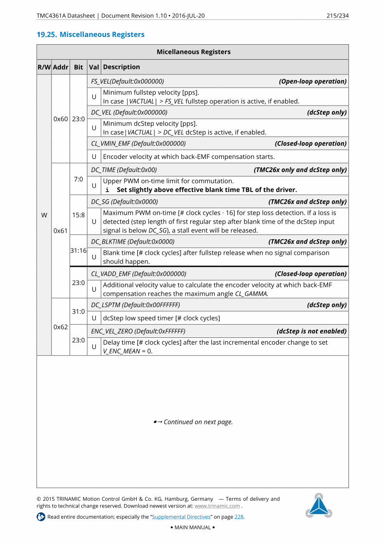
TMC4361A Datasheet | Document Revision 1.10 • 2016-JUL-20 215/234
© 2015 TRINAMIC Motion Control GmbH & Co. KG, Hamburg, Germany — Terms of delivery and
rights to technical change reserved. Download newest version at: www.trinamic.com .
Read entire documentation; especially the “Supplemental Directives” on page 228.
MAIN MANUAL
Miscellaneous Registers
Micellaneous Registers
R/W Addr Bit Val Description
W
0x60 23:0
FS_VEL(Default:0x000000) (Open-loop operation)
U Minimum fullstep velocity [pps].
In case |VACTUAL| > FS_VEL fullstep operation is active, if enabled.
DC_VEL (Default:0x000000) (dcStep only)
U Minimum dcStep velocity [pps].
In case|VACTUAL| > DC_VEL dcStep is active, if enabled.
CL_VMIN_EMF (Default:0x000000) (Closed-loop operation)
U Encoder velocity at which back-EMF compensation starts.
0x61
7:0
DC_TIME (Default:0x00) (TMC26x only and dcStep only)
U Upper PWM on-time limit for commutation.
i Set slightly above effective blank time TBL of the driver.
15:8
DC_SG (Default:0x0000) (TMC26x and dcStep only)
U
Maximum PWM on-time [# clock cycles ∙ 16] for step loss detection. If a loss is
detected (step length of first regular step after blank time of the dcStep input
signal is below DC_SG), a stall event will be released.
31:16
DC_BLKTIME (Default:0x0000) (TMC26x and dcStep only)
U Blank time [# clock cycles] after fullstep release when no signal comparison
should happen.
23:0
CL_VADD_EMF (Default:0x000000) (Closed-loop operation)
U Additional velocity value to calculate the encoder velocity at which back-EMF
compensation reaches the maximum angle CL_GAMMA.
0x62
31:0 DC_LSPTM (Default:0x00FFFFFF) (dcStep only)
U dcStep low speed timer [# clock cycles]
23:0
ENC_VEL_ZERO (Default:0xFFFFFF) (dcStep is not enabled)
U Delay time [# clock cycles] after the last incremental encoder change to set
V_ENC_MEAN = 0.
Continued on next page.

TMC4361A Datasheet | Document Revision 1.10 • 2016-JUL-20 216/234
© 2015 TRINAMIC Motion Control GmbH & Co. KG, Hamburg, Germany — Terms of delivery and
rights to technical change reserved. Download newest version at: www.trinamic.com .
Read entire documentation; especially the “Supplemental Directives” on page 228.
MAIN MANUAL
Micellaneous Registers
R/W Addr Bit Val Description
W 0x63
7:0
ENC_VMEAN_WAIT (Default:0x00) (incremental encoders only)
U
Delay period [# clock cycles] between two consecutive actual encoder velocity
values that account for calculaton of mean encoder velocity.
Set ENC_VMEAN_WAIT > 32. i Is set automatically to SER_PTIME for absolute SSI/SPI encoder.
7:0
SER_ENC_VARIATION (Default:0x00) (absolute encoders only)
U
Multiplier for maximum permitted serial encoder variation between consecutive
absolute encoder requests.
Maximum permitted value = ENC_VARIATION / 256 • 1/8 • ENC_IN_RES. If ENC_VARIATION = 0: Maximum permitted value = 1/8 • ENC_IN_RES.
11:8 ENC_VMEAN_FILTER (Default:0x0)
U Filter exponent to calculate mean encoder velocity.
31:16
ENC_VMEAN_INT (Default:0x0000) (incremental encoders only)
U Encoder velocity update time [# clock cycles].
i Minimum value is set automatically to 256.
31:16
CL_CYCLE (Default:0x0000) (absolute encoders only)
U Closed-loop control cycle [# clock cycles].
i Is set automatically to fastest possible cycle for ABN encoders.
W 0x64 31:0 Reserved. Set to 0x00000000.
R
0x65 31:0 V_ENC (Default:0x00000000)
S Actual encoder velocity [pps].
0x66 31:0 V_ENC_MEAN (Default:0x00000000)
S Filtered encoder velocity [pps].
W 0x67 23:0
VSTALL_LIMIT (Default:0x00000000)
U Stop on stall velocity limit [pps]:
Only above this limit an active stall leads to a stop on stall, if enabled.
W 0x7C 31:0
CIRCULAR_DEC (Default:0x000)
U
Decimal places for circular motion if one revolution is not exactly mapped to an
even number of µSteps per revolution.
Value representation: 1 digit and 31 decimal places.
W 0x7D
15:0
ENC_COMP_XOFFSET (Default:0x0000)
U Start offset for triangular compensation in horizontal direction.
0 ≤ ENC_COMP_XOFFSET < 216
23:16
ENC_COMP_YOFFSET (Default:0x00)
S Start offset for triangular compensation in vertical direction.
−128 ≤ ENC_COMP_YOFFSET ≤ 127
31:24 ENC_COMP_AMPL (Default:0x00)
U Maximum amplitude for encoder compensation.
Table 89: Miscellaneous Registers

TMC4361A Datasheet | Document Revision 1.10 • 2016-JUL-20 217/234
© 2015 TRINAMIC Motion Control GmbH & Co. KG, Hamburg, Germany — Terms of delivery and
rights to technical change reserved. Download newest version at: www.trinamic.com .
Read entire documentation; especially the “Supplemental Directives” on page 228.
MAIN MANUAL
Transfer Registers
Transfer Registers
R/W Addr Bit Val Description
W 0x68 31:0
ADDR_TO_ENC (Default:0x00000000) (SPI encoders only)
-
Address data permanently sent to get encoder angle data from the SPI encoder
slave device.
Address data sent from TMC4361A to SPI encoder for one-time data transfer.
W 0x69 31:0
DATA_TO_ENC (Default:0x00000000) (SPI encoders only)
- Configuration data sent from TMC4361A to SPI encoder for one-time data
transfer.
R 0x6A 31:0
ADDR_FROM_ENC (Default:0x00000000) (SPI encoders only)
-
Repeated request data is stored here.
Address data received from SPI encoder as response of the one-time data
transfer.
R 0x6B 31:0 DATA_FROM_ENC (Default:0x00000000) (SPI encoders only)
- Data received from SPI encoder as response of the one-time data transfer.
W
0x6C 31:0
COVER_LOW (Default:0x00000000)
-
Lower configuration bits of SPI orders that can be sent from TMC4361A to the
motor drivers via SPI output.
Automatic cover data transfer (automatic_cover = 1): Value in COVER_LOW are sent
in case |VACTUAL| crosses SPI_SWITCH_VEL downwards.
Set COVER_DATA_LENGTH ≤ 32. In case COVER_DATA_LENGTH = 0, no TMC2130 must be selected.
R POLLING_STATUS (Default:0x00000000) (TMC26x / TMC2130 only)
- DRV_STATUS response of TMC26x / TMC2130
W
0x6D
31:0
COVER_HIGH (Default:0x00000000)
-
Upper configuration bits of SPI orders that can be sent from TMC4361A to the
motor drivers via SPI output.
Automatic cover data transfer (automatic_cover = 1): Value in COVER_LOW are sent
if |VACTUAL| crosses SPI_SWITCH_VEL upwards.
Set COVER_DATA_LENGTH ≤ 32. In case COVER_DATA_LENGTH = 0, no TMC2130 must be selected.
R
POLLING_REG (Default:0x00000000) (TMC2130 only)
19:0 - LOST_STEPS response of TMC2130
27:20 - PWM_SCALE response of TMC2130
31:28 - GSTAT response of TMC2130
R 0x6E 31:0
COVER_DRV_LOW (Default:0x00000000)
- Lower configuration bits of SPI response received from the motor driver
connected to the SPI output.
R 0x6F 31:0
COVER_DRV_HIGH (Default:0x00000000)
- Upper configuration bits of SPI response received from the motor driver
connected to the SPI output.
Table 90: Transfer Registers

TMC4361A Datasheet | Document Revision 1.10 • 2016-JUL-20 218/234
© 2015 TRINAMIC Motion Control GmbH & Co. KG, Hamburg, Germany — Terms of delivery and
rights to technical change reserved. Download newest version at: www.trinamic.com .
Read entire documentation; especially the “Supplemental Directives” on page 228.
MAIN MANUAL
SinLUT Registers
SinLUT Registers
R/W Addr Bit Val Description
W
0x70
31:0
MSLUT[0] (Default:0xAAAAB554)
0x71 MSLUT[1] (Default:0x4A9554AA)
0x72 MSLUT[2] (Default:0x24492929)
0x73 MSLUT[3] (Default:0x10104222)
0x74 MSLUT[4] (Default:0xFBFFFFFF)
0x75 MSLUT[5] (Default:0xB5BB777D)
0x76 MSLUT[6] (Default:0x49295556)
0x 77 MSLUT[7] (Default:0x00404222)
- Each bit defines the difference between consecutive values in the
microstep look-up table MSLUT (in combination with MSLUTSEL).
W 0x78 31:0 MSLUTSEL (Default:0xFFFF8056)
- Definition of the four segments within each quarter MSLUT wave.
R
0x79 9:0
MSCNT (Default:0x000)
U Actual µStep position of the sine value.
W MSOFFSET (Default:0x000) (TMC23x/24x only)
U Microstep offset for PWM mode.
R 0x7A
8:0 CURRENTA (Default:0x000)
S Actual current value of coilA (sine values).
24:16 CURRENTB (Default:0x0F7)
S Actual current value of coilB (sine90_120 values).
R
0x7B
8:0 CURRENTA_SPI (Default:0x000)
S Actual scaled current value of coilA (sine values) that are sent to the driver.
24:16 CURRENTB_SPI (Default:0x0F7)
S Actual scaled current value of coilB (sine90_120 values); sent to motor driver.
W 31:0 TZEROWAIT (Default:0x00000000)
U Standstill phase after reaching VACTUAL = 0.
R 0x7C 8:0 SCALE_PARAM (Default:0x000)
U Actual used scale parameter.
W 0x7E
7:0 START_SIN (Default:0x00)
U Start value for sine waveform.
31:16 START_SIN90_120 (Default:0xF7)
U Start value for cosine waveform.
31:24
DAC_OFFSET (Default:0x00)
U Offset (absolute sine and cosine DAC values).
S Offset (mapped DAC values).
Table 91: SinLUT Registers

TMC4361A Datasheet | Document Revision 1.10 • 2016-JUL-20 219/234
© 2015 TRINAMIC Motion Control GmbH & Co. KG, Hamburg, Germany — Terms of delivery and
rights to technical change reserved. Download newest version at: www.trinamic.com .
Read entire documentation; especially the “Supplemental Directives” on page 228.
MAIN MANUAL
TMC Version Register
Version Register
R/W Addr Bit Val Description
R 0x7F 15:0 Version No (Default:0x0002)
U TMC4361 version number.
Table 92: Version Register

TMC4361A Datasheet | Document Revision 1.10 • 2016-JUL-20 220/234
© 2015 TRINAMIC Motion Control GmbH & Co. KG, Hamburg, Germany — Terms of delivery and
rights to technical change reserved. Download newest version at: www.trinamic.com .
Read entire documentation; especially the “Supplemental Directives” on page 228.
MAIN MANUAL
20. Absolute Maximum Ratings
The maximum ratings may not be exceeded under any circumstances. Operating the circuit at or near
more than one maximum rating at a time for extended periods shall be avoided by application design.
Maximum Ratings: 3.3V supply
Parameter (VCC = 3.3V nominal à TEST_MODE = 0V) Symbol Min Max Unit
Supply voltage VCC 3.0 3.6 V
Input voltage IO VIN −0.3 3.6 V
Table 93: Maximum Ratings: 3.3V supply
Maximum Ratings: 5.0V supply
Parameter (VCC = 5V nominal à TEST_MODE = 1.8V) Symbol Min Max Unit
Supply voltage VCC 4.8 5.2 V
Input voltage IO VIN −0.3 5.2 V
Table 94: Maximum Ratings: 5.0V supply
Maximum Ratings: Temperature
Parameter Symbol Min Max Unit
Temperature T −40 125 °C
Table 95: Maximum Ratings: Temperature

TMC4361A Datasheet | Document Revision 1.10 • 2016-JUL-20 221/234
© 2015 TRINAMIC Motion Control GmbH & Co. KG, Hamburg, Germany — Terms of delivery and
rights to technical change reserved. Download newest version at: www.trinamic.com .
Read entire documentation; especially the “Supplemental Directives” on page 228.
MAIN MANUAL
21. Electrical Characteristics
DC characteristics contain the spread of values guaranteed within the specified supply voltage range unless otherwise specified. Typical values represent the average value of all parts measured at +25°C. Temperature variation also causes stray to some values. A device with typical values will not leave Min/Max range within the full temperature range.
DC Characteristics
Parameter Symbol Conditions Min Typ Max Unit
Extended temperature range TCOM −40°C 125 °C
Nominal core voltage VDD 1.8 V
Nominal IO voltage VDD 3.3 / 5.0 V
Nominal input voltage VIN 0.0 3.3 / 5.0 V
Input voltage low level VINL VDD = 3.3V / 5V −0.3 0.8 / 1.2 V
Input voltage high level VINH VDD = 3.3V / 5V 2.3 / 3.5 3.6 / 5.2 V
Input with pull-down VIN = VDD 5 30 110 µA
Input with pull-up VIN = 0V −110 −30 −5 µA
Input low current VIN = 0V −10 10 µA
Input high current VIN = VDD −10 10 µA
Output voltage low level VOUTL VDD = 3.3V / 5V 0.4 V
Output voltage high level VOUTH VDD = 3.3V / 5V 2.64 / 4.0 V
Output driver strength IOUT_DRV VDD = 3.3V / 5V 4.0 mA
Table 96: DC Characteristics
Power Dissipation
Power Dissipation
Parameter Symbol Conditions Min Typ Max Unit
Static power dissipation PDSTAT All inputs at VDD or GND
VDD = 3.3V / 5V 1.1 / 1.7 mW
Dynamic power dissipation PDDYN
All inputs at VDD or GND
fCLK variable
VDD = 3.3V / 5V
2.7 / 4.0 mW / MHz
Total power dissipation PD fCLK = 16 MHz
VDD = 3.3V / 5V 44.3 / 65.7 mW
Table 97: Power Dissipation

TMC4361A Datasheet | Document Revision 1.10 • 2016-JUL-20 222/234
© 2015 TRINAMIC Motion Control GmbH & Co. KG, Hamburg, Germany — Terms of delivery and
rights to technical change reserved. Download newest version at: www.trinamic.com .
Read entire documentation; especially the “Supplemental Directives” on page 228.
MAIN MANUAL
General IO Timing Parameters
General IO Timing Parameters
Parameter Symbol Conditions Min Typ Max Unit
Operation frequency fCLK fCLK = 1 / tCLK 4.21) 16 30 MHz
Clock Period tCLK Rising edge to
rising edge 33.5 62.5 ns
Clock time low 16.5 ns
Clock time high 16.5 ns
CLK input signal rise time tRISE_IN 20 % to 80 % 20 ns
CLK input signal fall time tFALL_IN 80 % to 20 % 20 ns
Output signal rise time tRISE_OUT 20 % to 80 %
load 32 pF 3.5 ns
Output signal fall time tFALL_OUT 80 % to 20 %
load 32 pF 3.5 ns
Setup time for SPI input
signals in synchronous
design
tSU Relative to
rising clk edge 5 ns
Hold time tHD Relative to
rising clk edge 5 ns
Table 98: General IO Timing Parameters
1) The lower limit for fCLK refers to the limits of the internal unit conversion to physical units. The chip will also operate at
lower frequencies.

TMC4361A Datasheet | Document Revision 1.10 • 2016-JUL-20 223/234
© 2015 TRINAMIC Motion Control GmbH & Co. KG, Hamburg, Germany — Terms of delivery and
rights to technical change reserved. Download newest version at: www.trinamic.com .
Read entire documentation; especially the “Supplemental Directives” on page 228.
MAIN MANUAL
Layout Examples
Internal Circuit Diagram for Layout Example
Figure 73: Internal Circuit Diagram for Layout Example

TMC4361A Datasheet | Document Revision 1.10 • 2016-JUL-20 224/234
© 2015 TRINAMIC Motion Control GmbH & Co. KG, Hamburg, Germany — Terms of delivery and
rights to technical change reserved. Download newest version at: www.trinamic.com .
Read entire documentation; especially the “Supplemental Directives” on page 228.
MAIN MANUAL
Figure 74: Components Assembly for Application with Encoder
Figure 75: Top Layer: Assembly Side
Components Assembly for Application with Encoder
Top Layer: Assembly Side

TMC4361A Datasheet | Document Revision 1.10 • 2016-JUL-20 225/234
© 2015 TRINAMIC Motion Control GmbH & Co. KG, Hamburg, Germany — Terms of delivery and
rights to technical change reserved. Download newest version at: www.trinamic.com .
Read entire documentation; especially the “Supplemental Directives” on page 228.
MAIN MANUAL
Figure 76: Inner Layer (GND)
Figure 77: Inner Layer (Supply VS)
Inner Layer (GND)
Inner Layer (Supply VS)

TMC4361A Datasheet | Document Revision 1.10 • 2016-JUL-20 226/234
© 2015 TRINAMIC Motion Control GmbH & Co. KG, Hamburg, Germany — Terms of delivery and
rights to technical change reserved. Download newest version at: www.trinamic.com .
Read entire documentation; especially the “Supplemental Directives” on page 228.
MAIN MANUAL
Package Dimensions
Package Dimensions
Parameter Ref Min Nom Max Total thickness A 0.8 0.85 0.9
Stand off A1 0 0.03
5 0.05
Mold thickness A2 - 0.65 0.67
Lead frame thickness A3 0.203 REF
Lead width b 0.2 0.25 0.3
Body size X D 6 BSC
Body size Y E 6 BSC
Lead pitch e 0.5 BSC
Exposed die pad size X J 4.52 4.62 4.72
Exposed die pad size Y K 4.52 4.62 4.72
Lead length L 0.35 0.4 0.45
Package edge tolerance aaa 0.1
Mold flatness bbb 0.1
Coplanarity ccc 0.08
Lead offset ddd 0.1
Exposed pad offset eee 0.1
Table 99: Package Dimensions
Figure 78: Package Dimensional Drawings

TMC4361A Datasheet | Document Revision 1.10 • 2016-JUL-20 227/234
© 2015 TRINAMIC Motion Control GmbH & Co. KG, Hamburg, Germany — Terms of delivery and
rights to technical change reserved. Download newest version at: www.trinamic.com .
Read entire documentation; especially the “Supplemental Directives” on page 228.
MAIN MANUAL
Package Material Information
Please refer to the associated document “TMC43xx Package Material Information, V1.00” for information about available package dimensions and the various tray and reel package options. This document informs you about outside dimensions per tray and/reel and the number of ICs per tray/reel. It also provides information about available packaging units and their weight, as well as box dimension and weight details for outer packaging.
The document is available for download on the TMC4361A product page at www.trinamic.com.
i Should you require a custom-made component packaging solution or a different outer packaging
solution, or have questions pertaining to the component packaging choice, please contact our
customer service.
NOTE:
Our trays and reels are JEDEC-compliant.
Marking Details provided on single Chip
The marking on each single chip shows:
❶ Trinamic emblem.
❷ Product code.
❸ Date code.
❹ Location of the copyright holder,
which is TRINAMIC in Hamburg, Germany.
❺ Lot number.
Figure 79: Marking Details on Chip1
1 The image provided is not an accurate rendition of the original product but only serves as illustration.
❹
❸
❷
❶
❺

TMC4361A Datasheet | Document Revision 1.10 • 2016-JUL-20 228/234
© 2015 TRINAMIC Motion Control GmbH & Co. KG, Hamburg, Germany — Terms of delivery and
rights to technical change reserved. Download newest version at: www.trinamic.com .
Read entire documentation; especially the “Supplemental Directives” on page 228.
MAIN MANUAL
APPENDICES
22. Supplemental Directives
ESD-DEVICE INSTRUCTIONS
This product is an ESD-sensitive CMOS device. It is sensitive to electrostatic discharge.
Provide effective grounding to protect personnel and machines.
Ensure work is performed in a nonstatic environment.
Use personal ESD control footwear and ESD wrist straps, if necessary.
Failure to do so can result in defects, damages and decreased reliability.
The producer of the product TMC4361A is TRINAMIC GmbH & Co. KG in Hamburg,
Germany; hereafter referred to as TRINAMIC. TRINAMIC is the supplier; and in this
function provides the product and the production documentation to its
customers.
TRINAMIC owns the content of this user manual in its entirety, including but not
limited to pictures, logos, trademarks, and resources.
© Copyright 2015 TRINAMIC®. All rights reserved. Electronically published by
TRINAMIC®, Germany. All trademarks used are property of their respective
owners.
Redistributions of source or derived format (for example, Portable Document
Format or Hypertext Markup Language) must retain the above copyright notice,
and the complete Datasheet User Manual documentation of this product
including associated Application Notes; and a reference to other available
product-related documentation.
Trademark designations and symbols used in this documentation indicate that a
product or feature is owned and registered as trademark and,'or patent either by
TRINAMIC or by ather manufacturers, whose products are used or referred to in
combination With TRINAMlC's products and TRINAMlC's product documentation.
This documentation is a noncommercial publication that seeks to provide concise
scientific and technical user information to the target user. Thus, we only enter
trademark designations and symbols in the Short Spec of the documentation that
introduces the product at a quick glance. We also enter the trademark designation
'symbol when the product or feature name occurs for the first time in the
document. All trademarks used are property of their respective owners.
The documentation provided here, is for programmers and engineers only, who
are equipped with the necessary skills and have been trained to work with this
type of product.
The Target User knows how to responsibly make use of this product without
causing harm to himself or others, and without causing damage to systems or
devices, in which the user incorporates the product.
Producer Information
Copyright
Trademark Designations and Symbols
Target User

TMC4361A Datasheet | Document Revision 1.10 • 2016-JUL-20 229/234
© 2015 TRINAMIC Motion Control GmbH & Co. KG, Hamburg, Germany — Terms of delivery and
rights to technical change reserved. Download newest version at: www.trinamic.com .
Read entire documentation; especially the “Supplemental Directives” on page 228.
MAIN MANUAL
TRINAMIC Motion Control GmbH & Co. KG does not authorize or warrant any of
its products for use in life support systems, without the specific written consent
of TRINAMIC Motion Control GmbH & Co. KG.
Life support systems are equipment intended to support or sustain life, and
whose failure to perform, when properly used in accordance with instructions
provided, can be reasonably expected to result in personal injury or death.
Information given in this document is believed to be accurate and reliable.
However, no responsibility is assumed for the consequences of its use nor for any
infringement of patents or other rights of third parties which may result from its
use. Specifications are subject to change without notice.
The data specified in this user manual is intended solely for the purpose of
product description. No representations or warranties, either express or implied,
of merchantability, fitness for a particular purpose or of any other nature are
made hereunder with respect to information/specification or the products to
which information refers and no guarantee with respect to compliance to the
intended use is given.
In particular, this also applies to the stated possible applications or areas of
applications of the product. TRINAMIC products are not designed for and must
not be used in connection with any applications where the failure of such
products would reasonably be expected to result in significant personal injury or
death (Safety-Critical Applications) without TRINAMIC’s specific written consent.
TRINAMIC products are not designed nor intended for use in military or aerospace
applications or environments or in automotive applications unless specifically
designated for such use by TRINAMIC. TRINAMIC conveys no patent, copyright,
mask work right or other trade mark right to this product. TRINAMIC assumes no
liability for any patent and/or other trade mark rights of a third party resulting
from processing or handling of the product and/or any other use of the product.
This document Datasheet User Manual contains the User Information for the
Target User.
The Short Spec forms the preface of the document and is aimed at providing a
general product overview. The Main Manual contains detailed product
information pertaining to functions, and configuration settings. It contains all
other pages of this document.
This product documentation is related and/or associated with additional tool
kits, firmware and other items, as provided on the product page at:
www.trinamic.com .
Disclaimer: Life Support Systems
Disclaimer: Intended Use
Product Documentation Details
Collateral Documents & Tools

TMC4361A Datasheet | Document Revision 1.10 • 2016-JUL-20 230/234
© 2015 TRINAMIC Motion Control GmbH & Co. KG, Hamburg, Germany — Terms of delivery and
rights to technical change reserved. Download newest version at: www.trinamic.com .
Read entire documentation; especially the “Supplemental Directives” on page 228.
MAIN MANUAL
23. Tables Index
Table 1: TMC4361A Order Codes .......................................................................................................................... 2 Table 2: Pin Names and Descriptions ................................................................................................................. 12 Table 3: SPI Input Control Interface Pins ........................................................................................................... 16 Table 4: Read and Write Access Examples ......................................................................................................... 17 Table 5: SPI Interface Timing ............................................................................................................................... 19 Table 6: Input Filtering Groups (Assigned Pins) ................................................................................................ 20 Table 7: Input Filtering (Assigned Register) ....................................................................................................... 20 Table 8: Sample Rate Configuration ................................................................................................................... 21 Table 9: Configuration of Digital Filter Length .................................................................................................. 21 Table 10: Pins Names: Status Events .................................................................................................................. 24 Table 11:Register Names: Status Flags and Events .......................................................................................... 24 Table 12: Pin Names: Ramp Generator .............................................................................................................. 28 Table 13: Register Names: Ramp Generator ..................................................................................................... 28 Table 14: Overview of General and Basic Ramp Configuration Options ....................................................... 31 Table 15: Description of TMC4361A Motion Profiles ........................................................................................ 33 Table 16: Trapezoidal Ramps: AACTUAL Assignments during Motion .......................................................... 36 Table 17: Parameter Assignments for S-shaped Ramps.................................................................................. 39 Table 18: Minimum and Maximum Values if Real World Units are selected ................................................ 50 Table 19: Minimum and Maximum Values for Steep Slopes for fCLK =16MHz .............................................. 50 Table 20: Pins used for External Step Control ................................................................................................... 51 Table 21: Registers used for External Step Control .......................................................................................... 51 Table 22: Pins used for Reference Switches ...................................................................................................... 55 Table 23: Dedicated Registers for Reference Switches .................................................................................... 55 Table 24: Reference Configuration and Corresponding Transition of particular Reference Switch .......... 57 Table 25: Overview of different home_event Settings ..................................................................................... 61 Table 26: TARGET_REACHED Output Pin Configuration .................................................................................. 64 Table 27: Comparison Selection Grid to generate POS_COMP_REACHED_Flag ........................................... 65 Table 28: Circular motion (X_RANGE = 300) ....................................................................................................... 69 Table 29: Dedicated Ramp Timing Pins .............................................................................................................. 70 Table 30: Dedicated Ramp Timing Registers ..................................................................................................... 70 Table 31: Start Trigger Configuration ................................................................................................................. 71 Table 32: Start Enable Switch Configuration ..................................................................................................... 71 Table 33: Parameter Settings Timing Example 1 .............................................................................................. 73 Table 34: Parameter Settings Timing Example 2 .............................................................................................. 74 Table 35: Parameter Settings Timing Example 3 .............................................................................................. 75 Table 36: Pipeline Activation Options ................................................................................................................. 84 Table 37: Pipeline Mapping for different Pipeline Configurations ................................................................. 85 Table 38: Pin Names for SPI Motor Drive ........................................................................................................... 90 Table 39: Dedicated SPI Output Registers ......................................................................................................... 91 Table 40: Wave Inclination Characteristics of Internal MSLUT ....................................................................... 94 Table 41: Overview of the Microstep Behavior Example ................................................................................. 98 Table 42: SPI Output Communication Pins ........................................................................................................ 99 Table 43: TMC Stepper Motor Driver Options ................................................................................................. 104 Table 44: Mapping of TMC23x/24x Status Flags ............................................................................................. 108 Table 45: Mapping of TMC26x Status Flags ..................................................................................................... 116 Table 46: Mapping of TMC2130 Status Flags ................................................................................................... 120 Table 47: Non-TMC Data Transfer Options ..................................................................................................... 121 Table 48: Available SPI-DAC Options ................................................................................................................ 124 Table 49: Pin Description: NFREEZE .................................................................................................................. 133 Table 50: Pin Descriptions DFREEZE and IFREEZE .......................................................................................... 133

TMC4361A Datasheet | Document Revision 1.10 • 2016-JUL-20 231/234
© 2015 TRINAMIC Motion Control GmbH & Co. KG, Hamburg, Germany — Terms of delivery and
rights to technical change reserved. Download newest version at: www.trinamic.com .
Read entire documentation; especially the “Supplemental Directives” on page 228.
MAIN MANUAL
Table 51: Dedicated PWM Output Pins ............................................................................................................ 135 Table 52: Dedicated PWM Output Registers ................................................................................................... 135 Table 53: Dedicated dcStep Pins ....................................................................................................................... 140 Table 54: Dedicated dcStep Registers .............................................................................................................. 140 Table 55: Dedicated Decoder Unit Pins ................................................................................................................ 146 Table 56: Dedicated Decoder Unit Registers ........................................................................................................ 146 Table 57: Pin Assignment based on selected Encoder Setup ....................................................................... 148 Table 58: Index Channel Sensitivity .................................................................................................................. 151 Table 59: Supported SPI Encoder Data Transfer Modes ............................................................................... 161 Table 60: Dedicated Closed-Loop and PID Registers ........................................................................................... 163 Table 61: Dedicated Reset and Clock Pins ....................................................................................................... 174 Table 62: Dedicated Reset and Clock Gating Registers........................................................................................ 174 Table 63: Pin Names for Encoder Output Interface ....................................................................................... 177 Table 64: Dedicated SPI Output Registers ....................................................................................................... 177 Table 65: General Configuration 0x00.............................................................................................................. 182 Table 66: Reference Switch Configuration 0x01 ............................................................................................. 185 Table 67: Start Switch Configuration START_CONF 0x02 ............................................................................... 187 Table 68: Input Filter Configuration Register INPUT_FILT_CONF 0x03 ........................................................ 188 Table 69: SPI Output Configuration Register SPI_OUT_CONF 0x04 ............................................................. 191 Table 70: Current Scale Configuration (0x05) .................................................................................................. 192 Table 71: Current Scale Values (0x06) .............................................................................................................. 193 Table 72: Encoder Signal Configuration ENC_IN_CONF (0x07) ..................................................................... 197 Table 73: Serial Encoder Data Input Configuration ENC_IN_DATA (0x08) ................................................... 197 Table 74: Serial Encoder Data Output Configuration ENC_OUT_DATA (0x09) ............................................ 198 Table 75: Motor Driver Settings (0x0A) ............................................................................................................ 199 Table 76: Event Selection Regsiters 0x0B…0x0D ............................................................................................ 200 Table 77: Status Event Register EVENTS (0x0E) ............................................................................................... 201 Table 78: Status Flag Register STATUS (0x0F) .................................................................................................. 202 Table 79: Various Configuration Registers: Closed-loop, Switches, etc. ...................................................... 204 Table 80: Ramp Generator Registers ................................................................................................................ 208 Table 81: External Clock Frequency Register................................................................................................... 209 Table 82: Target and Compare Registers ......................................................................................................... 209 Table 83: External Clock Frequency Register................................................................................................... 210 Table 84: External Clock Frequency Register................................................................................................... 210 Table 85: Freeze Register ................................................................................................................................... 211 Table 86: Reset and Clock Gating Register ...................................................................................................... 211 Table 87: Encoder Registers............................................................................................................................... 213 Table 88: PID and Closed-Loop Registers ........................................................................................................ 214 Table 89: Miscellaneous Registers .................................................................................................................... 216 Table 90: Transfer Registers .............................................................................................................................. 217 Table 91: SinLUT Registers ................................................................................................................................. 218 Table 92: Version Register .................................................................................................................................. 219 Table 93: Maximum Ratings: 3.3V supply ........................................................................................................ 220 Table 94: Maximum Ratings: 5.0V supply ........................................................................................................ 220 Table 95: Maximum Ratings: Temperature ..................................................................................................... 220 Table 96: DC Characteristics .............................................................................................................................. 221 Table 97: Power Dissipation .............................................................................................................................. 221 Table 98: General IO Timing Parameters ......................................................................................................... 222 Table 99: Package Dimensions .......................................................................................................................... 226 Table 100: Document Revision History ............................................................................................................ 234

TMC4361A Datasheet | Document Revision 1.10 • 2016-JUL-20 232/234
© 2015 TRINAMIC Motion Control GmbH & Co. KG, Hamburg, Germany — Terms of delivery and
rights to technical change reserved. Download newest version at: www.trinamic.com .
Read entire documentation; especially the “Supplemental Directives” on page 228.
MAIN MANUAL
24. Figures Index
Figure 1: Sample Image TMC4361A Closed-Loop Drive ................................................................................... 1 Figure 2: Block Diagram ......................................................................................................................................... 1 Figure 3: S-shaped Velocity Profile ........................................................................................................................ 2 Figure 4: Hardware Set-up for Closed-loop Operation with TMC262 .............................................................. 2 Figure 5: Hardware Set-up for Open-loop Operation with TMC2130 .............................................................. 2 Figure 6: Package Outline: Pin Assignments Top View .................................................................................... 10 Figure 7: System Overview ................................................................................................................................... 13 Figure 8: TMC4361A Connection: VCC=3.3V ...................................................................................................... 14 Figure 9: TMC4361A with TMC26x Stepper Driver in SPI Mode or S/D Mode ............................................... 14 Figure 10: TMC4361A with TMC248 Stepper Driver in SPI Mode ................................................................... 15 Figure 11: TMC4361A with TMC2130 Stepper Driver in SPI Mode or S/D Mode .......................................... 15 Figure 12: TMC4361A SPI Datagram Structure ................................................................................................. 16 Figure 13: Difference between Read and Write Access ................................................................................... 17 Figure 14: SPI Timing Datagram .......................................................................................................................... 18 Figure 15: Reference Input Pins: SR_REF = 1, FILT_L_REF = 1 .......................................................................... 22 Figure 16: START Input Pin: SR_S = 2, FILT_L_S = 0 ............................................................................................ 22 Figure 17: Encoder Interface Input Pins: SR_ENC_IN = 0, FILT_L_ENC_IN = 7 ................................................ 22 Figure 18: Step/Dir Input Filter Parameter ........................................................................................................ 23 Figure 19: No Ramp Motion Profile .................................................................................................................... 34 Figure 20: Trapezoidal Ramp without Break Point ........................................................................................... 35 Figure 21: Trapezoidal Ramp with Break Point ................................................................................................. 35 Figure 22: S-shaped Ramp without initial and final Acceleration/Deceleration Values ............................... 37 Figure 23: S-shaped Ramp with initial and final Acceleration/Deceleration Values..................................... 38 Figure 24: Trapezoidal Ramp with initial Velocity ............................................................................................. 40 Figure 25: S-shaped Ramp with initial Start Velocity ........................................................................................ 41 Figure 26: S-shaped Ramp with Stop Velocity ................................................................................................... 43 Figure 27: S-shaped Ramp with Start and Stop Velocity .................................................................................. 44 Figure 28: S-shaped Ramps with combined VSTART and ASTART Parameters ............................................ 45 Figure 29: sixPoint Ramp: Trapezoidal Ramp with Start and Stop Velocity .................................................. 46 Figure 30: Example for U-Turn Behavior of sixPoint Ramp ............................................................................. 47 Figure 31: Example for U-Turn Behavior of S-shaped Ramp .......................................................................... 48 Figure 32: Direct transition via VACTUAL=0 for S-shaped Ramps .................................................................. 48 Figure 33: HOME_REF Monitoring and HOME_ERROR_FLAG .......................................................................... 62 Figure 34: Ramp Timing Example 1 .................................................................................................................... 73 Figure 35: Ramp Timing Example 2 .................................................................................................................... 74 Figure 36: Ramp Timing Example 3 .................................................................................................................... 75 Figure 37: Single-level Shadow Register Option to replace complete Ramp Motion Profile. ..................... 77 Figure 38: Double-stage Shadow Register Option 1, suitable for S-shaped Ramps. .................................. 78 Figure 39: Double-stage Shadow Register Option 2, suitable for Trapezoidal Ramps. ............................... 79 Figure 40: Double-Stage Shadow Register Option 3, suitable for Trapezoidal Ramps ................................ 80 Figure 41: SHADOW_MISS_CNT Parameter for several internal Start Signals .............................................. 81 Figure 42: Target Pipeline with Configuration Options .................................................................................... 83 Figure 43: Pipeline Example A ............................................................................................................................. 86 Figure 44: Pipeline Example B ............................................................................................................................. 86 Figure 45: Pipeline Example C ............................................................................................................................. 87 Figure 46: Pipeline Example D ............................................................................................................................. 87 Figure 47: Pipeline Example E.............................................................................................................................. 87 Figure 48: Pipeline Example F .............................................................................................................................. 87 Figure 49: Pipeline Example G ............................................................................................................................. 88 Figure 50: Pipeline Example H ............................................................................................................................. 88

TMC4361A Datasheet | Document Revision 1.10 • 2016-JUL-20 233/234
© 2015 TRINAMIC Motion Control GmbH & Co. KG, Hamburg, Germany — Terms of delivery and
rights to technical change reserved. Download newest version at: www.trinamic.com .
Read entire documentation; especially the “Supplemental Directives” on page 228.
MAIN MANUAL
Figure 51: LUT Programming Example ............................................................................................................... 92 Figure 52: MSLUT Curve with all possible Base Wave Inclinations (highest Inclination first) ..................... 97 Figure 53: SPI Output Datagram Timing .......................................................................................................... 100 Figure 54: Cover Data Register Composition (CDL – COVER_DATA_LENGTH) ............................................. 102 Figure 55: Scaling Example 1 ............................................................................................................................. 131 Figure 56: Scaling Example 2 ............................................................................................................................. 132 Figure 57: Calculation of PWM Duty Cycles (PWM_AMPL) ............................................................................. 137 Figure 58: TMC4361A connected with TMC23x/24x operating in SPI Mode or PWM Mode ..................... 138 Figure 59: dcStep extended Application Operation Area .............................................................................. 141 Figure 60: Velocity Profile with Impact through Overload Situation ............................................................ 143 Figure 61: Triangular Function that compensates Encoder Misalignments ................................................ 149 Figure 62: Outline of ABN Signals of an incremental Encoder ...................................................................... 151 Figure 63:Serial Data Output: Four Examples ................................................................................................. 157 Figure 64: SSI: SSI_IN_CLK_DELAY=0 ................................................................................................................. 158 Figure 65: SSI: SSI_IN_CLK_DELAY>SER_CLK_IN_HIGH.................................................................................... 158 Figure 66: Calculation of the Output Angle with appropriate CL_DELTA_P ................................................. 167 Figure 67: Closed-Loop Current Scaling ........................................................................................................... 170 Figure 68: Closed-Loop Current Scaling Timing Behavior ............................................................................. 171 Figure 69: Calculation of the actual Load Angle GAMMA .............................................................................. 172 Figure 70: Manual Clock Gating Activation and Wake-Up ............................................................................. 175 Figure 71: Automatic Clock Gating Activation and Wake-Up ......................................................................... 176 Figure 72: Example for SSI Output Configuration: M - Multiturn; S - Singleturn ........................................ 178 Figure 73: Internal Circuit Diagram for Layout Example ............................................................................... 223 Figure 74: Components Assembly for Application with Encoder ................................................................. 224 Figure 75: Top Layer: Assembly Side ................................................................................................................ 224 Figure 76: Inner Layer (GND) ............................................................................................................................. 225 Figure 77: Inner Layer (Supply VS) .................................................................................................................... 225 Figure 78: Package Dimensional Drawings ...................................................................................................... 226 Figure 79: Marking Details on Chip1 ................................................................................................................. 227

TMC4361A Datasheet | Document Revision 1.10 • 2016-JUL-20 234/234
© 2015 TRINAMIC Motion Control GmbH & Co. KG, Hamburg, Germany — Terms of delivery and
rights to technical change reserved. Download newest version at: www.trinamic.com .
Read entire documentation; especially the “Supplemental Directives” on page 228.
MAIN MANUAL
25. Revision History
Document Revision History
Version Date Author Description
1.00 2014-APR-11 HS, SD First complete version. New release variant, which is a
product upgrade of TMC4361.
1.10 2016-JUL-20 HS, SV
New chapter organization with additional information.
Specifically for:
Chapter 17: Reset and Clock Gating, page 174.
Chapter 18: Serial Encoder Output, page 177 .
New Layout, ANSI-compliant safety notices.
Table 100: Document Revision History