Embed Size (px)
Citation preview

FAULT LOCALIZATION TECHNIQUES I
EMT 361
SCHOOL OF MICROELECTRONIC
ENGINEERING
KUKUM

TOPICS OF INTEREST 1
OPTICAL MICROSCOPY
MECHANICAL PROBING
LIQUID CRYSTAL HOT SPOT DETECTION
EMISSION MICROSCOPY
SCANNING ELECTRON MICROSCOPY

Optical microscope

OPTICAL MICROSCOPE
1/a + 1/b = 1/f M= (Image Height)/(Object Height)
= b/a
QuickTime™ and aTIFF (Uncompressed) decompressor
are needed to see this picture.
QuickTime™ and aTIFF (Uncompressed) decompressor
are needed to see this picture.
QuickTime™ and aTIFF (Uncompressed) decompressor
are needed to see this picture.

real image - can be viewed on a screen, recorded on film, or projected onto the surface of a sensor such as a CCD or CMOS placed in the image plane. virtual image - cannot be viewed on a screen or recorded on film. a real image must be formed on the retina of the eye. When viewing specimens through the eyepieces of a microscope, a real image is formed on the retina, but it is actually perceived by the observer as a virtual image located approximately 10 inches (25 centimeters) in front of the eye.
QuickTime™ and aTIFF (Uncompressed) decompressor
are needed to see this picture.
QuickTime™ and aTIFF (Uncompressed) decompressor
are needed to see this picture.

Total visual magnification = objective magnification x eyepiece magnification.
5X objective with a 10X eyepiece = total visual magnification of 50X
100X objective with a 30X eyepiece = magnification of 3000X.
Total magnification is also dependent upon the tube length of the microscope. Most standard fixed tube length microscopes have a tube length of 160, 170, 200, or 210 mm- 160mm most common for transmitted light biomedical microscopes ; semiconductor industry, = 210mm.
additional magnification factor = tube factor in the user manuals provided by most microscope manufacturers. Thus, if a 5X objective is being used with a 15X set of eyepieces, then the total visual magnification becomes 93.75X (using a 1.25X tube factor) or 112.5X (using a 1.5X tube factor)
The objectives and eyepieces of these microscopes have optical properties designed for a specific tube length, and using an objective or eyepiece in a microscope of different tube length will lead to changes in the magnification factor (and may also lead to an increase in optical aberration lens errors). Infinity-corrected microscopes also have eyepieces and objectives that are optically-tuned to the design of the microscope, and these should not be interchanged between microscopes with different infinity tube lengths.
QuickTime™ and aTIFF (Uncompressed) decompressor
are needed to see this picture.
QuickTime™ and aTIFF (Uncompressed) decompressor
are needed to see this picture.
Objectives typically have magnifying powers that range from 1:1 (1X) to 100:1 (100X), with the most common powers being 4X (or 5X), 10X, 20X, 40X (or 50X), and 100X Eyepieces, magnification factors vary between 5X and 30X with the most commonly used eyepieces having a value of 10X-15X
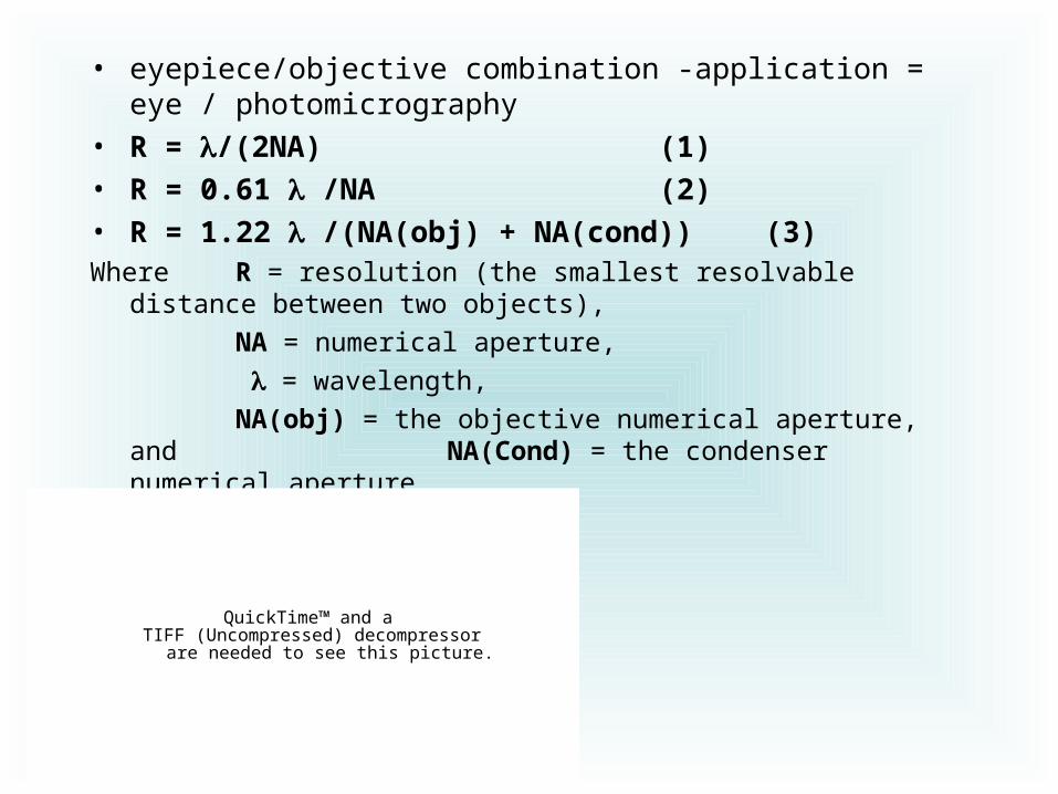
• eyepiece/objective combination -application = eye / photomicrography
• R = /(2NA) (1)• R = 0.61 /NA (2) • R = 1.22 /(NA(obj) + NA(cond)) (3) Where R = resolution (the smallest resolvable distance between two
objects),
NA = numerical aperture,
= wavelength,
NA(obj) = the objective numerical aperture, and NA(Cond) = the condenser numerical aperture
QuickTime™ and aTIFF (Uncompressed) decompressor
are needed to see this picture.

• Resolution and Numerical Aperture by Objective Type
Objective Type
Plan Achromat Plan Fluorite Plan Apochromat
M N.A R N.A R N.A R
4x 0.10 2.75 0.13 2.12 0.20 1.375
10x 0.25 1.10 0.30 0.92 0.45 0.61
20x 0.40 0.69 0.50 0.55 0.75 0.37
40x 0.65 0.42 0.75 0.37 0.95 0.29
60x 0.75 0.37 0.85 0.32 0.95 0.29
100x 1.25 0.22 1.30 0.21 1.40 0.20
N.A. = Numerical Aperture
R = Resolution (m)
M = Magnification
Resolution versus Wavelength
Wavelength (nm) Resolution (m) Colour360 .19 UV / Deep Blue400 .21 deep Blue450 .24 Blue500 .26 Blue/Green550 .29 Green/Orange600 .32 Orange/Red650 .34 Red700 .37
QuickTime™ and aTIFF (Uncompressed) decompressor
are needed to see this picture.

Mechanical Probing

QuickTime™ and aTIFF (Uncompressed) decompressor
are needed to see this picture.
QuickTime™ and aTIFF (Uncompressed) decompressor
are needed to see this picture.
QuickTime™ and aTIFF (Uncompressed) decompressor
are needed to see this picture.

Microprobing= probing= failure analysis technique used to achieve electrical contact with or access to a point in the active circuitry of the die. microprobing station = probe stationElectrical contact - fine-tipped probe needles directly on the point of interest, or on an area to which the point of interest is connected. Needle tip chosen - electrical contact needed & probing area. Micromanipulator - controlled by analyst to land the needle on the die precisely - optical / electron microscopeAnalyst employs the same thought process as when troubleshooting a full-size circuit. Microprobing = tool for analyst to access critical nodes on the microscopic die circuit while analyzing the behavior of the various parts of the circuit. Electrically pinpointing failure site = failure isolation => which requires the analyst to identify abnormal voltages and/or currents on the die. V and I measurements are performed by the voltmeters, curve tracers, oscilloscopes, attached to the probe needle through micromanipulator. Circuit excitation from voltage supplies, waveform generators, and the like may also be supplied to the die circuit in the same manner.

Passivation - hard, impenetrable - removal =RIE, LASERSchematic diagram & die lay-out of the device laser cutter - metal lines to be burned open for convenient isolation of nodes from one another Eye and hand coordination, as well as experience
Die scratches and even chip-outs landing four sharp probes within a 200 x 200 nm area with less than 5 nm precision = typical
The size of the minimum landing area is dependent on the sharpness of the probes. With FIB sharpened probes, the minimum landing area could be much smaller than that stated above. ICs - 90 nm node technology to 60 and then to 45 nmSETs?

four probes independently and linearly operated in X, Y, and Z with <5 nm precision. installed in a high-resolution SEM for precise imaging and probe placement similar to the arrangement shown Tungsten probes with a 45-degree bend were installed in the four positioners. The 90 nm node IC test chip was deprocessed to the contact level and etched for 5s in 20 parts H2O to 1 part 49% HF.
QuickTime™ and aTIFF (Uncompressed) decompressor
are needed to see this picture.
QuickTime™ and aTIFF (Uncompressed) decompressor
are needed to see this picture.
QuickTime™ and aTIFF (Uncompressed) decompressor
are needed to see this picture.
QuickTime™ and aTIFF (Uncompressed) decompressor
are needed to see this picture.

QuickTime™ and aTIFF (Uncompressed) decompressor
are needed to see this picture.
QuickTime™ and aTIFF (Uncompressed) decompressor
are needed to see this picture.
The IDVDS curves of an integrated n-channel MOSFET
The reverse bias of the device under test
This comparison is one way to determine if the device is functioning properly. The IDVDS curves are very similar which this shows that the current device under investigation is functioning as expected.

p-channel MOSFETs, the current ID flows when the gate voltage V GS is negative with respect to the source voltage V DS .
Typically, p-channel MOSFETs have a higher gate threshold voltage and lower saturation current. These p-channel curves, show the expected lower performance of a p-channel MOSFET in comparison with the n-channel MOSFET.
QuickTime™ and aTIFF (Uncompressed) decompressor
are needed to see this picture.

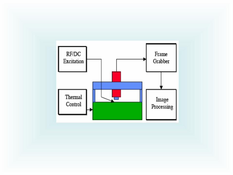
Liquid Crystal Hot Spot Detection

Microthermography = Hot Spot Detection = LCHD -locate areas on die surface that exhibit excessive heating - high current flow-- die defects or abnormalities like dielectric ruptures, metallization shorts, and leaky junctions.
Bias chosen - enough current to generate the amount of heat needed to change the visual characteristics of the liquid crystal
LC crystalline - 'smectic' phase and the 'nematic' phase.
@ higher T’s - 'isotropic phase,' = molecules are randomly located and randomly oriented

isotropic phase = a clear liquid, no distinctive optical characteristics because of the homogeneous distribution of its moleculesnematic phase = milky appearance & exhibits optical properties similar to those of crystal structuresVia optical microscope - polarizing filter in illumination path (polarizer) and a cross polarized filter in the viewing path (analyzer) :Isotropic films = black, since the cross polarized light is blocked by the analyzerNematic films = rainbow-colored, since light reflected from nematic films 'twist' such that they are able to pass through the analyzerHots spots raise the temperature of the liquid crystal, making it appear black at that spot. The die surface of a well-prepared sample with a hot spot will therefore appear as rainbow-colored, except for the hot spot which will appear as a blackened area.

correct amount.
Too thick = uniformly black=> impossible to detect nematic phase changes from temperature increases.
Too thin = streaks of dark and light grays=> hot spots less visible.
perfect = general area of the die surface rainbow-colored=> best contrast to a hot spot.
bias - defect site carries enough current to heat the liquid crystal at the hot spot, but not enough current to heat the entire liquid crystal film.
If hot spot generates so much heat that the entire die surface is darkened even at minimum power setting, excitation must be 'pulsed' or oscillated - locate the hot spot, which is the point of origin and return of the oscillating color contrast on the die surface.
Polarizing filters - adjusted to provide the best rainbow color for the liquid crystal film.
interpreting the presence / absence of hot spots on the die = something wrong; not always the actual failure site = good components forced to conduct high currents by an anomaly somewhere else in the circuit.
Complement with FA techniques in order to arrive at the right conclusion.
Dielectric Shorts or Breakdowns, Metallization Shorts, Junction Leakages, Mobile Ionic Contamination, etc
QuickTime™ and aTIFF (Uncompressed) decompressor
are needed to see this picture.

Emission Microscopy

QuickTime™ and aTIFF (Uncompressed) decompressor
are needed to see this picture.
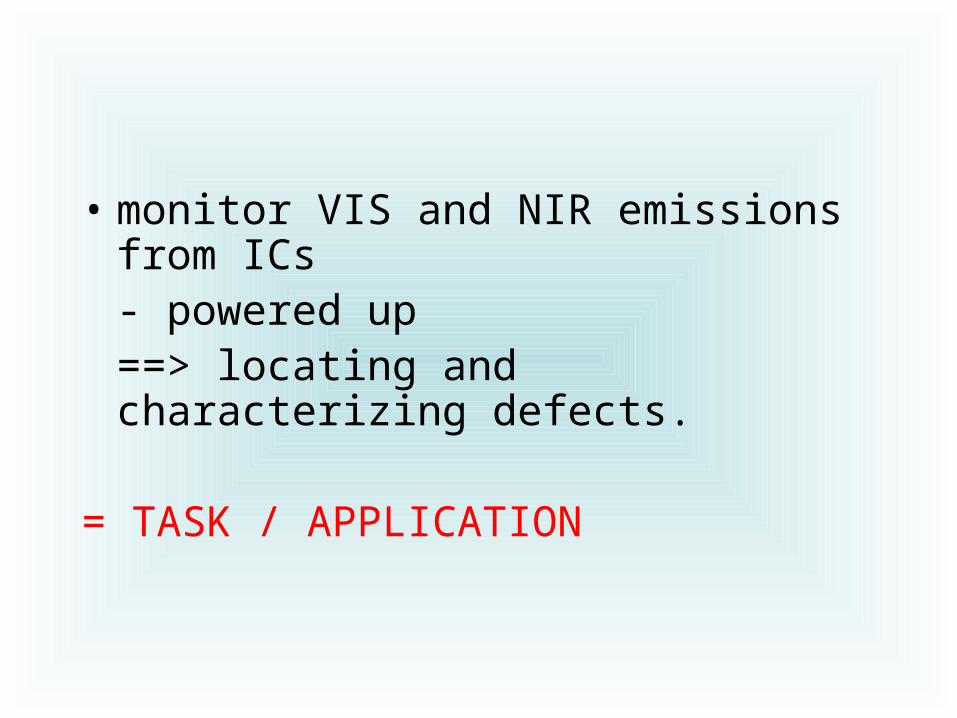
• monitor VIS and NIR emissions from ICs
- powered up ==> locating and
characterizing defects.
= TASK / APPLICATION

THEORY =
@ faulty junction / transistor,
hot charge carriers = e’s and h’s-will often be present in the component
during operation, and may have enough energy to result in weak visible emission during carrier recombination. Even
when they do not, lower carrier energies may result in NIR emission or even just local heating
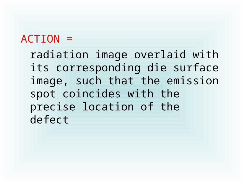
ACTION =
radiation image overlaid with its corresponding die surface image, such that the emission spot coincides with the precise location of the defect

TOOLS
• OPTICAL MICROSCOPE
• CCD CAMERA - VIS / NIR / BOLOMETER / IMAGE INTENSIFIER
• PC
• IMAGE PROCESSING SOFTWARE

applications include but are not limited to :
• 1) detection of previously unknown or undetectable electroluminescence ;
• 2) detection of avalanche luminescence from junction breakdowns,junction defects, currents due to saturated MOS transistors, and transistor hot electron effects;
• 3) detection of dielectric electroluminescence from current flow through SiO2 and Si3N4.

three common types
• simple emission microscopy • energy-resolved emission microscopy
(EREM) • backside die analysis
QuickTime™ and aTIFF (Uncompressed) decompressor
are needed to see this picture.

simple emission microscopy
- bias voltage applied to exposed IC - visible image of the device's weak emission is recorded in the dark. - compared to an ambient-light image of the same area,
allowing emitting defects to be located with great precision
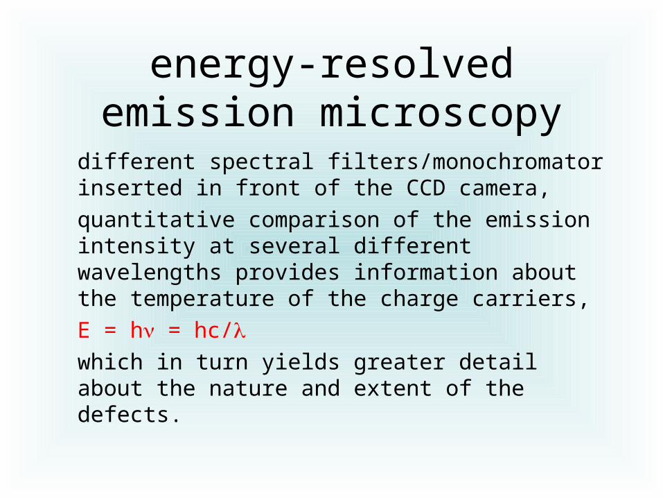
energy-resolved emission microscopy
different spectral filters/monochromator inserted in front of the CCD camera,
quantitative comparison of the emission intensity at several different wavelengths provides information about the temperature of the charge carriers,
E = h = hc/which in turn yields greater detail about the nature and extent of the defects.
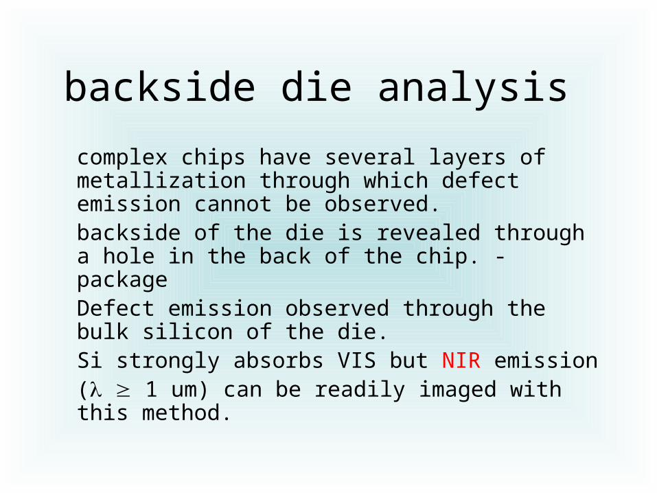
backside die analysis
complex chips have several layers of metallization through which defect emission cannot be observed. backside of the die is revealed through a hole in the back of the chip. - packageDefect emission observed through the bulk silicon of the die. Si strongly absorbs VIS but NIR emission ( 1 um) can be readily imaged with this method.


Scanning Electron Microscope
QuickTime™ and aTIFF (Uncompressed) decompressor
are needed to see this picture.

image is formed and presented by a very fine electron beam- focused on the surface of the specimen.
beam is scanned over specimen in a series of lines and frames called a raster- accomplished by means of small coils of wire carrying the controlling current (the scan coils).

specimen bombarded by e’s over a very small area.
-elastically reflected from the specimen, with no loss of energy.
-absorbed by the specimen and give rise to secondary electrons of very low energy, together with X- rays.
-absorbed and give rise to the emission of visible light (cathodoluminescence).
-give rise to electric currents within the specimen. All these effects can be used to produce an image. By far the most common, however, is image formation by means of the low-energy secondary electrons.

• 2ndary e’s are selectively attracted to a grid at a low (~50V) +ve potential with respect to the specimen.
• Behind the grid is a disc at ~10 kV +ve with respect to the specimen.
• Disc consists of a layer of scintillant coated with a thin layer of Al. 2ndary e’s pass through grid and strike disc - emission of light from the scintillant.
• The light to PMT - photons into voltage. Strength of this voltage depends on the number of secondary electrons that are striking the disc.
• The voltage to electronic console - processed and amplified to generate a point of brightness on CRT.
• Image built simply scanning e-beam across the specimen in exact synchrony with scan of the e-beam in CRT.

SEM does’nt have objective, intermediate and projector lenses to magnify the image as in the optical microscope. magnification results from the ratio of the area scanned on the specimen to the area of the television screen. Increasing mag. in SEM is achieved quite simply by scanning the electron beam over a smaller area of the specimen. Image formation in SEM equally applicable to elastically scattered electrons, X-rays, or photons of visible light - detection systems different in each case. Secondary electron imaging is the most common because it can be used with almost any specimen.

M> 300,000 X => semiconductor <3,000 X
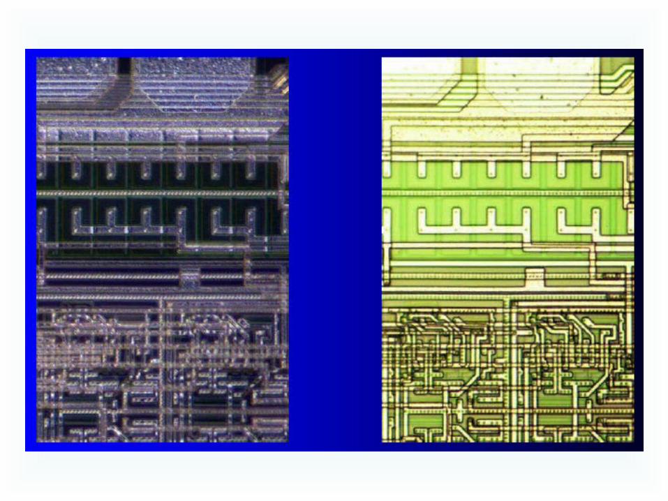
analysis of die/package cracks and fracture surfaces, bond failures, and physical defects on the die or package surface
energy of the primary electrons determines the quantity of secondary electrons collected - increases as the energy of the primary electron beam increases, until a certain limit - secondary electrons diminish as the energy of the primary beam increases, because the primary beam is already activating electrons deep below the surface. Deep electrons usually recombine before reaching the surface for emission.
emissions above 50 eV ~backscattered electrons.
Backscattered electron imaging distinguishing materials - yield of collected backscattered electrons increases monotonically with the specimen's atomic number. Backscatter imaging can distinguish elements with atomic number differences of at least 3, i.e., materials with atomic number differences of at least 3 would appear with good contrast on the image.
For example, inspecting the remaining Au on an Al bond pad after its Au ball bond has lifted off would be easier using backscatter imaging, since the Au islets would stand out from the Al background.

1) The EHT must be high enough to provide a good image but low enough to prevent specimen charging.
2) To maximize contrast due to material differences, use as low an EHT as possible.
3) If possible, sputter-coat the specimen to prevent specimen charging. Sputter-coating is considered destructive. Never sputter-coat units that still need to undergo electrical testing, curve tracing, EDX analysis, inspection, etc.
4) The probe current must be set to its default value, unless a higher probe current is needed to focus the point of interest properly.
Die/Package Cracks, Die Attach Failures/Defects, Bonding Failures/Defects, Wire Defects/Fractures, Lead Defects/Failures, Foreign Materials on Die/Package, Die Surface Defects, Seal Cracks/Defects, etc.

QuickTime™ and aTIFF (Uncompressed) decompressor
are needed to see this picture.
QuickTime™ and aTIFF (Uncompressed) decompressor
are needed to see this picture.
The GaAs RF IC we investigated could fail because of opens at R 1or shorts at C 1or C 1.
A curve-tracer's display shows the current-vs.-voltage plot from tests on the RF input pin of the circuit shown in Figure 1. The positive and negative resistance changes indicate problems with internal components
QuickTime™ and aTIFF (Uncompressed) decompressor
are needed to see this picture.
QuickTime™ and aTIFF (Uncompressed) decompressor
are needed to see this picture.
A visible-light photo of a failed device shows a small spot revealed by liquid-crystal material. This hot spot indicates a short circuit.
An image from SEM shows the trench etched around a defective capacitor by a laser. (The arrow points to the defects' location.)

QuickTime™ and aTIFF (Uncompressed) decompressor
are needed to see this picture.
QuickTime™ and aTIFF (Uncompressed) decompressor
are needed to see this picture.
(a) The bump on a defective GaAs RF IC, as seen in this SEM image, indicated the location of a short circuit. Compare the bump in (a) to the known ESD defect—also a short circuit—shown in (b)

References
• http://micro.magnet.fsu.edu/primer/anatomy/anatomy.html
• http://www.semiconfareast.com/lem.htm