Embed Size (px)
Citation preview

FactoryLink 7Version 7.0
Device Interface Guide
FactoryLink Device Interface Guide
• • • • • • • • • • • • • • • • • • • • • • • • • • • •

© Copyright 2000 United States Data Corporation. All rights reserved.
NOTICE:
The information contained in this document (and other media provided herewith) constitutes confidential information of United States Data Corporation (“USDATA”) and is protected by copyright laws and international copyright treaties, as well as other intellectual property laws and treaties. Such information is not to be disclosed, used or copied by, or transferred to, any individual, corporation, company or other entity, in any form, by any means or for any purpose, without the express written permission of USDATA.
The information contained in this document and related media constitutes documentation relating to a software product and is being provided solely for use with such software product. The software product was provided pursuant to a separate license or other agreement and such information is subject to the restrictions and other terms and conditions of such license or other agreement.
The information contained in this document and related media is subject to change without notice and does not represent a commitment on the part of USDATA. Except for warranties, if any, set forth in the separate license or other agreement relating to the applicable software product, USDATA makes no warranty, express or implied, with respect to such information or such software product.
USDATA and FactoryLink are registered trademarks of United States Data Corporation in the United States and/or other countries. Open Software Bus is a registered trademark licensed to United States Data Corporation. All other brand or product names are trademarks or registered trademarks of their respective holders.
.
•
•
•
•

FactoryLink Device Interface Guide / 3
Part I External Device Interface
Chapter 1 External Device Interface Overview . . . . . . . . . . . . . . . . . . . . . . . . . . . . 19Communications Methodology . . . . . . . . . . . . . . . . . . . . . . . . . . . . . . . . . . . . . . . . . . . . . 20Communicating with Multiple Devices . . . . . . . . . . . . . . . . . . . . . . . . . . . . . . . . . . . . . . 22Communicating with Multiple Protocol Modules . . . . . . . . . . . . . . . . . . . . . . . . . . . . . . . 23Device Topologies . . . . . . . . . . . . . . . . . . . . . . . . . . . . . . . . . . . . . . . . . . . . . . . . . . . . . . . 27
Serial Port . . . . . . . . . . . . . . . . . . . . . . . . . . . . . . . . . . . . . . . . . . . . . . . . . . . . . . . 27DigiBoard Port . . . . . . . . . . . . . . . . . . . . . . . . . . . . . . . . . . . . . . . . . . . . . . . . . . . 28Ethernet Board Port . . . . . . . . . . . . . . . . . . . . . . . . . . . . . . . . . . . . . . . . . . . . . . . . 28Combination . . . . . . . . . . . . . . . . . . . . . . . . . . . . . . . . . . . . . . . . . . . . . . . . . . . . . 29
Components of a Communication Path . . . . . . . . . . . . . . . . . . . . . . . . . . . . . . . . . . . . . . . 31Retrieving and Transferring Data . . . . . . . . . . . . . . . . . . . . . . . . . . . . . . . . . . . . . . . . . . . 35
Triggered Read Operations . . . . . . . . . . . . . . . . . . . . . . . . . . . . . . . . . . . . . . . . . . 35Unsolicited Read Operations . . . . . . . . . . . . . . . . . . . . . . . . . . . . . . . . . . . . . . . . . 36Write Operations . . . . . . . . . . . . . . . . . . . . . . . . . . . . . . . . . . . . . . . . . . . . . . . . . . 37
Tag Naming Considerations for EDI . . . . . . . . . . . . . . . . . . . . . . . . . . . . . . . . . . . . . . . . . 39Triggering Considerations . . . . . . . . . . . . . . . . . . . . . . . . . . . . . . . . . . . . . . . . . . . . . . . . . 40
How Shared Memory Works . . . . . . . . . . . . . . . . . . . . . . . . . . . . . . . . . . . . . . . . . . 41How to Avoid Filling Up Shared Memory . . . . . . . . . . . . . . . . . . . . . . . . . . . . . . . . 44
Configuration Considerations . . . . . . . . . . . . . . . . . . . . . . . . . . . . . . . . . . . . . . . . . . . . . . 45Triggered Read Operations . . . . . . . . . . . . . . . . . . . . . . . . . . . . . . . . . . . . . . . . . . 45Unsolicited Read Operations . . . . . . . . . . . . . . . . . . . . . . . . . . . . . . . . . . . . . . . . . 46Write Operations . . . . . . . . . . . . . . . . . . . . . . . . . . . . . . . . . . . . . . . . . . . . . . . . . . 46Triggering Guidelines . . . . . . . . . . . . . . . . . . . . . . . . . . . . . . . . . . . . . . . . . . . . . . 47Optimization Guidelines . . . . . . . . . . . . . . . . . . . . . . . . . . . . . . . . . . . . . . . . . . . . . 48
The Cable Connection . . . . . . . . . . . . . . . . . . . . . . . . . . . . . . . . . . . . . . . . . . . . . . . . . . . . 50
Chapter 2 Tag Definition Dialog . . . . . . . . . . . . . . . . . . . . . . . . . . . . . . . . . . . . . . . 51
Chapter 3 Setting Operating System Parameters . . . . . . . . . . . . . . . . . . . . . . . . . . 53Windows NT Ethernet . . . . . . . . . . . . . . . . . . . . . . . . . . . . . . . . . . . . . . . . . . . . . . . . . . . . 53
Chapter 4 Setting Up Serial Communications . . . . . . . . . . . . . . . . . . . . . . . . . . . . 55Electrical Interface Signals . . . . . . . . . . . . . . . . . . . . . . . . . . . . . . . . . . . . . . . . . . . . . . . . 56

4 / FactoryLink Device Interface Guide
•
•
•
•
RS-232 Mechanical Interface Standard Reference . . . . . . . . . . . . . . . . . . . . . . . . . . . . . . 57Cable Description and Diagrams . . . . . . . . . . . . . . . . . . . . . . . . . . . . . . . . . . . . . . . . . . . . 59Worksheet for Cable Connections . . . . . . . . . . . . . . . . . . . . . . . . . . . . . . . . . . . . . . . . . . . 62Using ComWiz to Configure Ports . . . . . . . . . . . . . . . . . . . . . . . . . . . . . . . . . . . . . . . . . . 64
Chapter 5 Configuring Communication Paths . . . . . . . . . . . . . . . . . . . . . . . . . . . . 69Identifying Protocol Types and Defining Logical Ports . . . . . . . . . . . . . . . . . . . . . . . . . . 70
Completing the Logical Station Worksheet . . . . . . . . . . . . . . . . . . . . . . . . . . . . . . . 71Creating the Logical Port Definitions . . . . . . . . . . . . . . . . . . . . . . . . . . . . . . . . . . . 73Sample External Device Definition Table Entries . . . . . . . . . . . . . . . . . . . . . . . . . . 75
Creating Logical Station Definitions . . . . . . . . . . . . . . . . . . . . . . . . . . . . . . . . . . . . . . . . . 77Modicon Modbus Plus Logical Station Table . . . . . . . . . . . . . . . . . . . . . . . . . . . . . 80Sample Logical Station Table Entries . . . . . . . . . . . . . . . . . . . . . . . . . . . . . . . . . . . 85
Table Entries for Sample Worksheet . . . . . . . . . . . . . . . . . . . . . . . . . . . . . . . . . . . . . . . . . 87
Chapter 6 Reading Data from a Device . . . . . . . . . . . . . . . . . . . . . . . . . . . . . . . . . 89Triggered Read Request . . . . . . . . . . . . . . . . . . . . . . . . . . . . . . . . . . . . . . . . . . . . . . . . . . 90Unsolicited Read Request . . . . . . . . . . . . . . . . . . . . . . . . . . . . . . . . . . . . . . . . . . . . . . . . . 91Defining the Table Type and Triggers . . . . . . . . . . . . . . . . . . . . . . . . . . . . . . . . . . . . . . . . 92
Triggered Read Request . . . . . . . . . . . . . . . . . . . . . . . . . . . . . . . . . . . . . . . . . . . . . 93Unsolicited Read Request . . . . . . . . . . . . . . . . . . . . . . . . . . . . . . . . . . . . . . . . . . . . 96Combination Read Request . . . . . . . . . . . . . . . . . . . . . . . . . . . . . . . . . . . . . . . . . . 97
Specifying What to Read and Where to Store It . . . . . . . . . . . . . . . . . . . . . . . . . . . . . . . . 98Read Holding or Input Register, Store in Analog Element . . . . . . . . . . . . . . . . . . . 102Read Holding or Input Register, Store in Digital Element . . . . . . . . . . . . . . . . . . . 104Read Holding Register, Store in Floating-Point or Long Analog Element . . . . . . . 106Read Holding Register, Store in Message Element . . . . . . . . . . . . . . . . . . . . . . . . 108Read Coil or Input Status Register, Store in Digital Element . . . . . . . . . . . . . . . . . 110Read Memory Register, Store in Analog Element . . . . . . . . . . . . . . . . . . . . . . . . . 112Read Statistics Word, Store in Analog Element . . . . . . . . . . . . . . . . . . . . . . . . . . . 114Read Global Data Word, Store in Analog Element . . . . . . . . . . . . . . . . . . . . . . . . 116
Sample Read Requests . . . . . . . . . . . . . . . . . . . . . . . . . . . . . . . . . . . . . . . . . . . . . . . . . . 118Sample Triggered Read Request . . . . . . . . . . . . . . . . . . . . . . . . . . . . . . . . . . . . . . 118Sample Unsolicited Read Request . . . . . . . . . . . . . . . . . . . . . . . . . . . . . . . . . . . . 121

FactoryLink Device Interface Guide / 5
Chapter 7 Writing Data to a Device . . . . . . . . . . . . . . . . . . . . . . . . . . . . . . . . . . . 123Block Write Request . . . . . . . . . . . . . . . . . . . . . . . . . . . . . . . . . . . . . . . . . . . . . . . . . . . . 124Exception Write Request . . . . . . . . . . . . . . . . . . . . . . . . . . . . . . . . . . . . . . . . . . . . . . . . . 125Defining the Table Type and Triggers . . . . . . . . . . . . . . . . . . . . . . . . . . . . . . . . . . . . . . . 126
Block Write Request . . . . . . . . . . . . . . . . . . . . . . . . . . . . . . . . . . . . . . . . . . . . . . . 127Exception Write Request . . . . . . . . . . . . . . . . . . . . . . . . . . . . . . . . . . . . . . . . . . . . 130Combination Write Request . . . . . . . . . . . . . . . . . . . . . . . . . . . . . . . . . . . . . . . . . 132
Specifying What to Write and Where to Write It . . . . . . . . . . . . . . . . . . . . . . . . . . . . . . 133Write Analog Element Value to Holding Register . . . . . . . . . . . . . . . . . . . . . . . . . 137Write Digital Element Value to Holding Register . . . . . . . . . . . . . . . . . . . . . . . . . 138Set Bits in Holding Register Using Mask Write . . . . . . . . . . . . . . . . . . . . . . . . . . . 141Write Floating-Point or Long Analog Element Value to Holding Register . . . . . . . 143Write Message Element Value to Holding Register . . . . . . . . . . . . . . . . . . . . . . . . 145Write Digital Element Value to Coil Register . . . . . . . . . . . . . . . . . . . . . . . . . . . . 147Write Analog Element Value to Memory Register . . . . . . . . . . . . . . . . . . . . . . . . . 149Write Analog Element Value to Global Data Word . . . . . . . . . . . . . . . . . . . . . . . . 151
Sample Write Requests . . . . . . . . . . . . . . . . . . . . . . . . . . . . . . . . . . . . . . . . . . . . . . . . . . 153Sample Triggered Block Write Request . . . . . . . . . . . . . . . . . . . . . . . . . . . . . . . . . 153Sample Exception Write Request . . . . . . . . . . . . . . . . . . . . . . . . . . . . . . . . . . . . . 156Sample Combination Write Request . . . . . . . . . . . . . . . . . . . . . . . . . . . . . . . . . . . 159
Chapter 8 Application Design Tips and Techniques . . . . . . . . . . . . . . . . . . . . . . . 163Grouping of Data . . . . . . . . . . . . . . . . . . . . . . . . . . . . . . . . . . . . . . . . . . . . . . . . . . . . . . . 164Processing Differences in Read and Write Operations . . . . . . . . . . . . . . . . . . . . . . . . . . 166
Processing of Read Operations . . . . . . . . . . . . . . . . . . . . . . . . . . . . . . . . . . . . . . 166Processing of Write Operations . . . . . . . . . . . . . . . . . . . . . . . . . . . . . . . . . . . . . . 168Read and Write Examples . . . . . . . . . . . . . . . . . . . . . . . . . . . . . . . . . . . . . . . . . . . 169
Specifying Priority . . . . . . . . . . . . . . . . . . . . . . . . . . . . . . . . . . . . . . . . . . . . . . . . . . . . . 171Overtriggering . . . . . . . . . . . . . . . . . . . . . . . . . . . . . . . . . . . . . . . . . . . . . . . . . . . . . . . . . 172Efficient Triggering . . . . . . . . . . . . . . . . . . . . . . . . . . . . . . . . . . . . . . . . . . . . . . . . . . . . . 172
Timed . . . . . . . . . . . . . . . . . . . . . . . . . . . . . . . . . . . . . . . . . . . . . . . . . . . . . . . . . . 172Cascaded . . . . . . . . . . . . . . . . . . . . . . . . . . . . . . . . . . . . . . . . . . . . . . . . . . . . . . . 172Self-Triggered . . . . . . . . . . . . . . . . . . . . . . . . . . . . . . . . . . . . . . . . . . . . . . . . . . . 174
Chapter 9 Testing and Troubleshooting . . . . . . . . . . . . . . . . . . . . . . . . . . . . . . . . 177EDI Flowcharts . . . . . . . . . . . . . . . . . . . . . . . . . . . . . . . . . . . . . . . . . . . . . . . . . . . . . . . . 178

6 / FactoryLink Device Interface Guide
•
•
•
•
Basic Troubleshooting . . . . . . . . . . . . . . . . . . . . . . . . . . . . . . . . . . . . . . . . . . . . . 179Common Errors . . . . . . . . . . . . . . . . . . . . . . . . . . . . . . . . . . . . . . . . . . . . . . . . . . 180Testing Your Application . . . . . . . . . . . . . . . . . . . . . . . . . . . . . . . . . . . . . . . . . . . 181
Verifying Proper Communications . . . . . . . . . . . . . . . . . . . . . . . . . . . . . . . . . . . . . . . . . 182
Chapter 10 Messages and Codes . . . . . . . . . . . . . . . . . . . . . . . . . . . . . . . . . . . . . . . 185Message Formats . . . . . . . . . . . . . . . . . . . . . . . . . . . . . . . . . . . . . . . . . . . . . . . . . . . . . . . 186
EDI Run-Time Manager Line Format . . . . . . . . . . . . . . . . . . . . . . . . . . . . . . . . . . 186Tag Message Format . . . . . . . . . . . . . . . . . . . . . . . . . . . . . . . . . . . . . . . . . . . . . . 186
Messages . . . . . . . . . . . . . . . . . . . . . . . . . . . . . . . . . . . . . . . . . . . . . . . . . . . . . . . . . . . . . 188EDI Messages . . . . . . . . . . . . . . . . . . . . . . . . . . . . . . . . . . . . . . . . . . . . . . . . . . . 189Startup Messages . . . . . . . . . . . . . . . . . . . . . . . . . . . . . . . . . . . . . . . . . . . . . . . . . 194
Chapter 11 Allen-Bradley . . . . . . . . . . . . . . . . . . . . . . . . . . . . . . . . . . . . . . . . . . . . 195Configuring the Logical Station Control Panel . . . . . . . . . . . . . . . . . . . . . . . . . . . . . . . . 196Configuring the Logical Station Information Panel . . . . . . . . . . . . . . . . . . . . . . . . . . . . 200Configuring the Read/Write Control Panel . . . . . . . . . . . . . . . . . . . . . . . . . . . . . . . . . . . 202Configuring the Read/Write Information Panel . . . . . . . . . . . . . . . . . . . . . . . . . . . . . . . 209Allen-Bradley Data Types . . . . . . . . . . . . . . . . . . . . . . . . . . . . . . . . . . . . . . . . . . . . . . . . 212Conversion of Data Types for Read Operations . . . . . . . . . . . . . . . . . . . . . . . . . . . . . . . 213
Digital Elements . . . . . . . . . . . . . . . . . . . . . . . . . . . . . . . . . . . . . . . . . . . . . . . . . 213Analog Elements . . . . . . . . . . . . . . . . . . . . . . . . . . . . . . . . . . . . . . . . . . . . . . . . . 213Floating-Point Elements . . . . . . . . . . . . . . . . . . . . . . . . . . . . . . . . . . . . . . . . . . . 214Longana Elements . . . . . . . . . . . . . . . . . . . . . . . . . . . . . . . . . . . . . . . . . . . . . . . . 215Message Elements . . . . . . . . . . . . . . . . . . . . . . . . . . . . . . . . . . . . . . . . . . . . . . . . 216
Conversion of Elements for Write Operations . . . . . . . . . . . . . . . . . . . . . . . . . . . . . . . . 217Digital Elements . . . . . . . . . . . . . . . . . . . . . . . . . . . . . . . . . . . . . . . . . . . . . . . . . 217Analog Elements . . . . . . . . . . . . . . . . . . . . . . . . . . . . . . . . . . . . . . . . . . . . . . . . . 217Floating-Point Elements . . . . . . . . . . . . . . . . . . . . . . . . . . . . . . . . . . . . . . . . . . . 218Longana Elements . . . . . . . . . . . . . . . . . . . . . . . . . . . . . . . . . . . . . . . . . . . . . . . . 219Message Elements . . . . . . . . . . . . . . . . . . . . . . . . . . . . . . . . . . . . . . . . . . . . . . . . 220
Allen-Bradley Address Entries . . . . . . . . . . . . . . . . . . . . . . . . . . . . . . . . . . . . . . . . . . . . 221PLC-2 Addresses . . . . . . . . . . . . . . . . . . . . . . . . . . . . . . . . . . . . . . . . . . . . . . . . . 221PLC-3 Addresses . . . . . . . . . . . . . . . . . . . . . . . . . . . . . . . . . . . . . . . . . . . . . . . . . 222Examples (Symbolic File Addressing) . . . . . . . . . . . . . . . . . . . . . . . . . . . . . . . . . 226PLC-5 Addresses . . . . . . . . . . . . . . . . . . . . . . . . . . . . . . . . . . . . . . . . . . . . . . . . . 226

FactoryLink Device Interface Guide / 7
PLC 5-250 Native Mode Addresses . . . . . . . . . . . . . . . . . . . . . . . . . . . . . . . . . . . 228Allen-Bradley Switch Setup . . . . . . . . . . . . . . . . . . . . . . . . . . . . . . . . . . . . . . . . . . . . . . 231
1770-KF2 Series B . . . . . . . . . . . . . . . . . . . . . . . . . . . . . . . . . . . . . . . . . . . . . . . . 2311771-KA2 . . . . . . . . . . . . . . . . . . . . . . . . . . . . . . . . . . . . . . . . . . . . . . . . . . . . . . . 2311771-KE . . . . . . . . . . . . . . . . . . . . . . . . . . . . . . . . . . . . . . . . . . . . . . . . . . . . . . . 2311771-KG . . . . . . . . . . . . . . . . . . . . . . . . . . . . . . . . . . . . . . . . . . . . . . . . . . . . . . . 2321785-KA . . . . . . . . . . . . . . . . . . . . . . . . . . . . . . . . . . . . . . . . . . . . . . . . . . . . . . . 232
Run-Time Application Messages . . . . . . . . . . . . . . . . . . . . . . . . . . . . . . . . . . . . . . . . . . 233Single-Digit Codes . . . . . . . . . . . . . . . . . . . . . . . . . . . . . . . . . . . . . . . . . . . . . . . . 233Double-Digit Codes . . . . . . . . . . . . . . . . . . . . . . . . . . . . . . . . . . . . . . . . . . . . . . . 234
Chapter 12 General Electric . . . . . . . . . . . . . . . . . . . . . . . . . . . . . . . . . . . . . . . . . . 237Configuring the Logical Station Control Panel . . . . . . . . . . . . . . . . . . . . . . . . . . . . . . . . 238Configuring the Logical Station Information Panel . . . . . . . . . . . . . . . . . . . . . . . . . . . . 241Configuring the Read/Write Control Panel . . . . . . . . . . . . . . . . . . . . . . . . . . . . . . . . . . . 244Configuring the Read/Write Information Panel . . . . . . . . . . . . . . . . . . . . . . . . . . . . . . . 251Run-Time Application Messages . . . . . . . . . . . . . . . . . . . . . . . . . . . . . . . . . . . . . . . . . . 255
ER:xxxx . . . . . . . . . . . . . . . . . . . . . . . . . . . . . . . . . . . . . . . . . . . . . . . . . . . . . . . . 255Single-Digit Codes . . . . . . . . . . . . . . . . . . . . . . . . . . . . . . . . . . . . . . . . . . . . . . . . 256Double-Digit Codes . . . . . . . . . . . . . . . . . . . . . . . . . . . . . . . . . . . . . . . . . . . . . . . 257
Chapter 13 General Purpose Interface . . . . . . . . . . . . . . . . . . . . . . . . . . . . . . . . . . 259Application Programs . . . . . . . . . . . . . . . . . . . . . . . . . . . . . . . . . . . . . . . . . . . . . . . . . . . 260Capabilities, Limitations, and Trade-Offs . . . . . . . . . . . . . . . . . . . . . . . . . . . . . . . . . . . . 261
Capabilities . . . . . . . . . . . . . . . . . . . . . . . . . . . . . . . . . . . . . . . . . . . . . . . . . . . . . 261Limitations . . . . . . . . . . . . . . . . . . . . . . . . . . . . . . . . . . . . . . . . . . . . . . . . . . . . . . 261Trade-Offs and Compromises in Design . . . . . . . . . . . . . . . . . . . . . . . . . . . . . . . . 261
Accessing the Configuration Panels . . . . . . . . . . . . . . . . . . . . . . . . . . . . . . . . . . . . . . . . 262Configuring the Logical Station Control Panel . . . . . . . . . . . . . . . . . . . . . . . . . . . . . . . . 263Configuring the Logical Station Information Panel . . . . . . . . . . . . . . . . . . . . . . . . . . . . 267GPI Command/Response Table . . . . . . . . . . . . . . . . . . . . . . . . . . . . . . . . . . . . . . . . . . . . 269
Command Table . . . . . . . . . . . . . . . . . . . . . . . . . . . . . . . . . . . . . . . . . . . . . . . . . . 270Response Table . . . . . . . . . . . . . . . . . . . . . . . . . . . . . . . . . . . . . . . . . . . . . . . . . . 270
Configuring the Command/Response Control Panel . . . . . . . . . . . . . . . . . . . . . . . . . . . 271Configuring the Command/Response Information Panel . . . . . . . . . . . . . . . . . . . . . . . . 275Flexibility and Design of the GPI . . . . . . . . . . . . . . . . . . . . . . . . . . . . . . . . . . . . . . . . . . 283Formatting an Outgoing Message . . . . . . . . . . . . . . . . . . . . . . . . . . . . . . . . . . . . . . . . . . 284

8 / FactoryLink Device Interface Guide
•
•
•
•
Format and Sources of Information in the Outgoing Message . . . . . . . . . . . . . . . 284Sample Information Panel for a Command Table . . . . . . . . . . . . . . . . . . . . . . . . . 286
Debugging Tools . . . . . . . . . . . . . . . . . . . . . . . . . . . . . . . . . . . . . . . . . . . . . . . . . . . . . . . 288Status/Debug Levels . . . . . . . . . . . . . . . . . . . . . . . . . . . . . . . . . . . . . . . . . . . . . . . 288RAW VALUE . . . . . . . . . . . . . . . . . . . . . . . . . . . . . . . . . . . . . . . . . . . . . . . . . . . . 288STAT_TAG . . . . . . . . . . . . . . . . . . . . . . . . . . . . . . . . . . . . . . . . . . . . . . . . . . . . . . 288
Summary of Basic Concepts . . . . . . . . . . . . . . . . . . . . . . . . . . . . . . . . . . . . . . . . . . . . . . 289GPI Functions . . . . . . . . . . . . . . . . . . . . . . . . . . . . . . . . . . . . . . . . . . . . . . . . . . . . . . . . . 291
Principles of Operation . . . . . . . . . . . . . . . . . . . . . . . . . . . . . . . . . . . . . . . . . . . . 291Defining the Outgoing Message . . . . . . . . . . . . . . . . . . . . . . . . . . . . . . . . . . . . . . 291Formatting the Incoming Response . . . . . . . . . . . . . . . . . . . . . . . . . . . . . . . . . . . 294Associating an Outgoing Message with an Incoming Response . . . . . . . . . . . . . . 295Specifying Methods to Detect an End-of-Response . . . . . . . . . . . . . . . . . . . . . . . . 297Non-Printable or “Don’t Care” Characters . . . . . . . . . . . . . . . . . . . . . . . . . . . . . 298Initiating a Transmission . . . . . . . . . . . . . . . . . . . . . . . . . . . . . . . . . . . . . . . . . . . 299Putting the Protocol Module in Unsolicited Mode . . . . . . . . . . . . . . . . . . . . . . . . 299Reporting Message Status . . . . . . . . . . . . . . . . . . . . . . . . . . . . . . . . . . . . . . . . . . 300Converting a Field’s Value . . . . . . . . . . . . . . . . . . . . . . . . . . . . . . . . . . . . . . . . . . 301
Using Process Functions . . . . . . . . . . . . . . . . . . . . . . . . . . . . . . . . . . . . . . . . . . . . . . . . . 302Associating a Digital Element to a Bit . . . . . . . . . . . . . . . . . . . . . . . . . . . . . . . . . 302Determining the Sources of Field Values . . . . . . . . . . . . . . . . . . . . . . . . . . . . . . . 303Modifying a Previously Defined Field . . . . . . . . . . . . . . . . . . . . . . . . . . . . . . . . . 304
GPI Configuration . . . . . . . . . . . . . . . . . . . . . . . . . . . . . . . . . . . . . . . . . . . . . . . . . . . . . . 305Configuration Example . . . . . . . . . . . . . . . . . . . . . . . . . . . . . . . . . . . . . . . . . . . . 305Command/Response Information Panel Entries . . . . . . . . . . . . . . . . . . . . . . . . . . 306Defining the Outgoing Message to the GPI . . . . . . . . . . . . . . . . . . . . . . . . . . . . . 316Defining Response Termination and Status Elements . . . . . . . . . . . . . . . . . . . . . . 318Defining the Incoming Response to the GPI . . . . . . . . . . . . . . . . . . . . . . . . . . . . . 319
Using Process Functions . . . . . . . . . . . . . . . . . . . . . . . . . . . . . . . . . . . . . . . . . . . . . . . . . 320Process Functions Table . . . . . . . . . . . . . . . . . . . . . . . . . . . . . . . . . . . . . . . . . . . . 320
Using Conversion Functions . . . . . . . . . . . . . . . . . . . . . . . . . . . . . . . . . . . . . . . . . . . . . . 323Sample Protocols . . . . . . . . . . . . . . . . . . . . . . . . . . . . . . . . . . . . . . . . . . . . . . . . . . . . . . . 326
Response Protocols . . . . . . . . . . . . . . . . . . . . . . . . . . . . . . . . . . . . . . . . . . . . . . . 326Command Protocols . . . . . . . . . . . . . . . . . . . . . . . . . . . . . . . . . . . . . . . . . . . . . . . 328Network Response Protocols . . . . . . . . . . . . . . . . . . . . . . . . . . . . . . . . . . . . . . . . 330Network Command Protocols . . . . . . . . . . . . . . . . . . . . . . . . . . . . . . . . . . . . . . . . 332
Run-Time Application Messages . . . . . . . . . . . . . . . . . . . . . . . . . . . . . . . . . . . . . . . . . . 334GPI Error Codes . . . . . . . . . . . . . . . . . . . . . . . . . . . . . . . . . . . . . . . . . . . . . . . . . 334

FactoryLink Device Interface Guide / 9
Chapter 14 Modicon Modbus . . . . . . . . . . . . . . . . . . . . . . . . . . . . . . . . . . . . . . . . . 341Configuring the Logical Station Control Panel . . . . . . . . . . . . . . . . . . . . . . . . . . . . . . . . 342Configuring the Logical Station Information Panel . . . . . . . . . . . . . . . . . . . . . . . . . . . . 344Configuring the Read/Write Control Panel . . . . . . . . . . . . . . . . . . . . . . . . . . . . . . . . . . . 346Configuring the Read/Write Information Panel . . . . . . . . . . . . . . . . . . . . . . . . . . . . . . . 353Run-Time Application Messages . . . . . . . . . . . . . . . . . . . . . . . . . . . . . . . . . . . . . . . . . . 358
Run-Time Manager Codes . . . . . . . . . . . . . . . . . . . . . . . . . . . . . . . . . . . . . . . . . . 358In Message Tags . . . . . . . . . . . . . . . . . . . . . . . . . . . . . . . . . . . . . . . . . . . . . . . . . . 360
Chapter 15 Modicon Modbus Plus . . . . . . . . . . . . . . . . . . . . . . . . . . . . . . . . . . . . . 363Configuring the Logical Station Control Panel . . . . . . . . . . . . . . . . . . . . . . . . . . . . . . . . 364Configuring the Logical Station Information Panel . . . . . . . . . . . . . . . . . . . . . . . . . . . . 366Configuring the Read/Write Control Panel . . . . . . . . . . . . . . . . . . . . . . . . . . . . . . . . . . . 369Configuring the Read/Write Information Panel . . . . . . . . . . . . . . . . . . . . . . . . . . . . . . . 376Modbus Plus Cable Diagram . . . . . . . . . . . . . . . . . . . . . . . . . . . . . . . . . . . . . . . . . . . . . . 383Run-Time Application Messages . . . . . . . . . . . . . . . . . . . . . . . . . . . . . . . . . . . . . . . . . . 384
Run-Time Messages . . . . . . . . . . . . . . . . . . . . . . . . . . . . . . . . . . . . . . . . . . . . . . . 385
Chapter 16 OMRON . . . . . . . . . . . . . . . . . . . . . . . . . . . . . . . . . . . . . . . . . . . . . . . . 389Configuring the Logical Station Control Panel . . . . . . . . . . . . . . . . . . . . . . . . . . . . . . . . 390Configuring the Logical Station Information Panel . . . . . . . . . . . . . . . . . . . . . . . . . . . . 393Configuring the Read/Write Control Panel . . . . . . . . . . . . . . . . . . . . . . . . . . . . . . . . . . . 396Configuring the Read/Write Information Panel . . . . . . . . . . . . . . . . . . . . . . . . . . . . . . . 403Technical Notes: Monitor Mode . . . . . . . . . . . . . . . . . . . . . . . . . . . . . . . . . . . . . . . . . . . 407OMRON Data Types and PLC Data Areas . . . . . . . . . . . . . . . . . . . . . . . . . . . . . . . . . . . 408Run-Time Application Messages . . . . . . . . . . . . . . . . . . . . . . . . . . . . . . . . . . . . . . . . . . 409
OMRON Error Codes . . . . . . . . . . . . . . . . . . . . . . . . . . . . . . . . . . . . . . . . . . . . . . 410
Chapter 17 Siemens CP525 . . . . . . . . . . . . . . . . . . . . . . . . . . . . . . . . . . . . . . . . . . . 417Configuring the Logical Station Control Panel . . . . . . . . . . . . . . . . . . . . . . . . . . . . . . . . 418Configuring the Logical Station Information Panel . . . . . . . . . . . . . . . . . . . . . . . . . . . . 421Configuring the Read/Write Control Panel . . . . . . . . . . . . . . . . . . . . . . . . . . . . . . . . . . . 423Configuring the Read/Write Information Panel . . . . . . . . . . . . . . . . . . . . . . . . . . . . . . . 430Siemens CP525 Switches . . . . . . . . . . . . . . . . . . . . . . . . . . . . . . . . . . . . . . . . . . . . . . . . 434Siemens CP525 Data Types . . . . . . . . . . . . . . . . . . . . . . . . . . . . . . . . . . . . . . . . . . . . . . . 435Run-Time Application Messages . . . . . . . . . . . . . . . . . . . . . . . . . . . . . . . . . . . . . . . . . . 438

10 / FactoryLink Device Interface Guide
•
•
•
•
Chapter 18 Siemens H1 . . . . . . . . . . . . . . . . . . . . . . . . . . . . . . . . . . . . . . . . . . . . . 441Siemens H1 Communications . . . . . . . . . . . . . . . . . . . . . . . . . . . . . . . . . . . . . . . . . . . . . 441
Types of Communication . . . . . . . . . . . . . . . . . . . . . . . . . . . . . . . . . . . . . . . . . . . 441Defining a TSAP Pair . . . . . . . . . . . . . . . . . . . . . . . . . . . . . . . . . . . . . . . . . . . . . 443TSAP IDs and ASCII Equivalents . . . . . . . . . . . . . . . . . . . . . . . . . . . . . . . . . . . . . 444
Accessing the Siemens H1 Tables . . . . . . . . . . . . . . . . . . . . . . . . . . . . . . . . . . . . . . . . . . 445Configuring the Logical Station Control Panel . . . . . . . . . . . . . . . . . . . . . . . . . . . . . . . . 446Configuring the Logical Station Information Panel . . . . . . . . . . . . . . . . . . . . . . . . . . . . 450Configuring the Read/Write Control Panel . . . . . . . . . . . . . . . . . . . . . . . . . . . . . . . . . . . 455Configuring the Read/Write Information Panel . . . . . . . . . . . . . . . . . . . . . . . . . . . . . . . 463Logical Station Commands . . . . . . . . . . . . . . . . . . . . . . . . . . . . . . . . . . . . . . . . . . . . . . . 474
Activate/Deactivate Station Command . . . . . . . . . . . . . . . . . . . . . . . . . . . . . . . . . 474Set Remote Parameters Command . . . . . . . . . . . . . . . . . . . . . . . . . . . . . . . . . . . . 475Set Logical Station Variables Command . . . . . . . . . . . . . . . . . . . . . . . . . . . . . . . . 482
Cable Diagrams . . . . . . . . . . . . . . . . . . . . . . . . . . . . . . . . . . . . . . . . . . . . . . . . . . . . . . . . 487Thick Net Bus . . . . . . . . . . . . . . . . . . . . . . . . . . . . . . . . . . . . . . . . . . . . . . . . . . . . 487Thin Net Bus . . . . . . . . . . . . . . . . . . . . . . . . . . . . . . . . . . . . . . . . . . . . . . . . . . . . 488
Siemens H1 Data Types . . . . . . . . . . . . . . . . . . . . . . . . . . . . . . . . . . . . . . . . . . . . . . . . . . 489Siemens H1 Adapter Display Utility (H1MPDISP) . . . . . . . . . . . . . . . . . . . . . . . . . . . . 493Run-Time Application Messages . . . . . . . . . . . . . . . . . . . . . . . . . . . . . . . . . . . . . . . . . . 494
Run-Time Logical Station Command Error Codes . . . . . . . . . . . . . . . . . . . . . . . . 496
Chapter 19 Square D . . . . . . . . . . . . . . . . . . . . . . . . . . . . . . . . . . . . . . . . . . . . . . . 499Configuring the Logical Station Control Panel . . . . . . . . . . . . . . . . . . . . . . . . . . . . . . . . 500Configuring the Logical Station Information Panel . . . . . . . . . . . . . . . . . . . . . . . . . . . . 504Configuring the Read/Write Control Panel . . . . . . . . . . . . . . . . . . . . . . . . . . . . . . . . . . . 507Configuring the Read/Write Information Panel . . . . . . . . . . . . . . . . . . . . . . . . . . . . . . . 515Cable Diagram . . . . . . . . . . . . . . . . . . . . . . . . . . . . . . . . . . . . . . . . . . . . . . . . . . . . . . . . . 518Run-Time Application Messages . . . . . . . . . . . . . . . . . . . . . . . . . . . . . . . . . . . . . . . . . . 519
SQRD8023 Messages . . . . . . . . . . . . . . . . . . . . . . . . . . . . . . . . . . . . . . . . . . . . . . 519SQRDRCOM and SQRDSCOM Messages . . . . . . . . . . . . . . . . . . . . . . . . . . . . . . 520SQRDRCOM, SQRDSCOM and SQRDENET Messages . . . . . . . . . . . . . . . . . . . . 520
Chapter 20 Texas Instruments . . . . . . . . . . . . . . . . . . . . . . . . . . . . . . . . . . . . . . . . 523Texas Instruments Setup . . . . . . . . . . . . . . . . . . . . . . . . . . . . . . . . . . . . . . . . . . . . . . . . . 524
DIP Switches . . . . . . . . . . . . . . . . . . . . . . . . . . . . . . . . . . . . . . . . . . . . . . . . . . . . 524

FactoryLink Device Interface Guide / 11
Baud Rate . . . . . . . . . . . . . . . . . . . . . . . . . . . . . . . . . . . . . . . . . . . . . . . . . . . . . . 526Timeout . . . . . . . . . . . . . . . . . . . . . . . . . . . . . . . . . . . . . . . . . . . . . . . . . . . . . . . . 527DIP Switches for TIWAY NIM . . . . . . . . . . . . . . . . . . . . . . . . . . . . . . . . . . . . . . . 528
Accessing the Texas Instruments Tables . . . . . . . . . . . . . . . . . . . . . . . . . . . . . . . . . . . . . 529Configuring the Unilink Setup Table . . . . . . . . . . . . . . . . . . . . . . . . . . . . . . . . . . . . . . . 530Configuring the Logical Station Control Panel . . . . . . . . . . . . . . . . . . . . . . . . . . . . . . . . 534Configuring the Logical Station Information Panel . . . . . . . . . . . . . . . . . . . . . . . . . . . . 537Configuring the Read/Write Control Panel . . . . . . . . . . . . . . . . . . . . . . . . . . . . . . . . . . . 540Configuring the Read/Write Information Panel . . . . . . . . . . . . . . . . . . . . . . . . . . . . . . . 547Loop Indexing . . . . . . . . . . . . . . . . . . . . . . . . . . . . . . . . . . . . . . . . . . . . . . . . . . . . . . . . . 554
Configuring Tables for Loop Indexing . . . . . . . . . . . . . . . . . . . . . . . . . . . . . . . . . 554Additional Parameters for TI Data Types . . . . . . . . . . . . . . . . . . . . . . . . . . . . . . . . . . . . 564
DCP . . . . . . . . . . . . . . . . . . . . . . . . . . . . . . . . . . . . . . . . . . . . . . . . . . . . . . . . . . . 564LRDS, LRRC, LRST, and LSDB . . . . . . . . . . . . . . . . . . . . . . . . . . . . . . . . . . . . . . 565
Computations for 5TI Sequencer Ladder Logic Code . . . . . . . . . . . . . . . . . . . . . . . . . . 567Diagram A: Bit Layout for 16-bit Sequencer Word . . . . . . . . . . . . . . . . . . . . . . . . 567Diagram B: Binary Weight Tables for Bits 10-15 . . . . . . . . . . . . . . . . . . . . . . . . . 568Diagram C: Sample Computations . . . . . . . . . . . . . . . . . . . . . . . . . . . . . . . . . . . . 568
Run-Time Application Messages . . . . . . . . . . . . . . . . . . . . . . . . . . . . . . . . . . . . . . . . . . 569Decoding ER: . . . . . . . . . . . . . . . . . . . . . . . . . . . . . . . . . . . . . . . . . . . . . . . . . . . 569Case 1: EDI Task or Protocol Module Errors . . . . . . . . . . . . . . . . . . . . . . . . . . . . 569Case 2: TIWAY Serial Unilink Network or Point-to-Point TI PLC Errors . . . . . . . 572Texas Instruments Message Strings . . . . . . . . . . . . . . . . . . . . . . . . . . . . . . . . . . . 580
Part II KTDTL and NetDTL
KTDTL and NetDTL at a Glance . . . . . . . . . . . . . . . . . . . . . . . . . . . . . 587
Chapter 21 KTDTL and NetDTL Overview . . . . . . . . . . . . . . . . . . . . . . . . . . . . . . 589Offlink Addressing Overview . . . . . . . . . . . . . . . . . . . . . . . . . . . . . . . . . . . . . . . . . . . . . 592KTDTL Topology . . . . . . . . . . . . . . . . . . . . . . . . . . . . . . . . . . . . . . . . . . . . . . . . . . . . . . 595NetDTL Topology . . . . . . . . . . . . . . . . . . . . . . . . . . . . . . . . . . . . . . . . . . . . . . . . . . . . . . 598
Chapter 22 Getting Started . . . . . . . . . . . . . . . . . . . . . . . . . . . . . . . . . . . . . . . . . . . 601Configuring the System Configuration Table . . . . . . . . . . . . . . . . . . . . . . . . . . . . . . . . . 602Optimizing Task Performance . . . . . . . . . . . . . . . . . . . . . . . . . . . . . . . . . . . . . . . . . . . . . 607

12 / FactoryLink Device Interface Guide
•
•
•
•
Chapter 23 Configuring Communication Paths . . . . . . . . . . . . . . . . . . . . . . . . . . . 609Logical Station Concepts . . . . . . . . . . . . . . . . . . . . . . . . . . . . . . . . . . . . . . . . . . . . . . . . . 611Creating Logical Station Definitions . . . . . . . . . . . . . . . . . . . . . . . . . . . . . . . . . . . . . . . . 613Sample Logical Station Table Entries . . . . . . . . . . . . . . . . . . . . . . . . . . . . . . . . . . . . . . . 631
Path and Address Entries . . . . . . . . . . . . . . . . . . . . . . . . . . . . . . . . . . . . . . . . . . . 634Logical Station Entries . . . . . . . . . . . . . . . . . . . . . . . . . . . . . . . . . . . . . . . . . . . . . 640
Chapter 24 Reading and Writing Data . . . . . . . . . . . . . . . . . . . . . . . . . . . . . . . . . . 645Reading Data from a Device . . . . . . . . . . . . . . . . . . . . . . . . . . . . . . . . . . . . . . . . . . . . . . 646Writing Data to a Device . . . . . . . . . . . . . . . . . . . . . . . . . . . . . . . . . . . . . . . . . . . . . . . . . 649Configuration Tips and Techniques . . . . . . . . . . . . . . . . . . . . . . . . . . . . . . . . . . . . . . . . . 652
Verifying Proper Communications . . . . . . . . . . . . . . . . . . . . . . . . . . . . . . . . . . . . 652Choosing Operation Type . . . . . . . . . . . . . . . . . . . . . . . . . . . . . . . . . . . . . . . . . . . 654Choosing Effective Triggering Schemes . . . . . . . . . . . . . . . . . . . . . . . . . . . . . . . . 656Configuring Read and Write Tables . . . . . . . . . . . . . . . . . . . . . . . . . . . . . . . . . . . 656
Configuring Triggered Read, Block Write, or Exception Write . . . . . . . . . . . . . . . . . . . 659Filling Out the Read/Write Control Panel . . . . . . . . . . . . . . . . . . . . . . . . . . . . . . 659Filling Out the Read/Write Information Panel . . . . . . . . . . . . . . . . . . . . . . . . . . . 667
Configuring an Unsolicited Read . . . . . . . . . . . . . . . . . . . . . . . . . . . . . . . . . . . . . . . . . . 670Unsolicited Read Operation Concepts . . . . . . . . . . . . . . . . . . . . . . . . . . . . . . . . . 670Filling Out the Unsolicited Read Control Panel . . . . . . . . . . . . . . . . . . . . . . . . . . 676Filling Out the Unsolicited Read Information Panel . . . . . . . . . . . . . . . . . . . . . . . 678
Sample Read and Write Table Entries . . . . . . . . . . . . . . . . . . . . . . . . . . . . . . . . . . . . . . . 680Sample Triggered Read Request . . . . . . . . . . . . . . . . . . . . . . . . . . . . . . . . . . . . . . 680Sample Unsolicited Read Request . . . . . . . . . . . . . . . . . . . . . . . . . . . . . . . . . . . . 682Sample Block Write Request . . . . . . . . . . . . . . . . . . . . . . . . . . . . . . . . . . . . . . . . . 683Sample Exception Write Request . . . . . . . . . . . . . . . . . . . . . . . . . . . . . . . . . . . . . 686
Techniques for Improving Communication Performance . . . . . . . . . . . . . . . . . . . . . . . . 688Specifying Priority . . . . . . . . . . . . . . . . . . . . . . . . . . . . . . . . . . . . . . . . . . . . . . . . 688Overtriggering . . . . . . . . . . . . . . . . . . . . . . . . . . . . . . . . . . . . . . . . . . . . . . . . . . . 689Efficient Triggering . . . . . . . . . . . . . . . . . . . . . . . . . . . . . . . . . . . . . . . . . . . . . . . 689
Chapter 25 Allen-Bradley Data Types and Addresses . . . . . . . . . . . . . . . . . . . . . . . 695Supported Data Types . . . . . . . . . . . . . . . . . . . . . . . . . . . . . . . . . . . . . . . . . . . . . . . . . . . 696Address Specification Formats . . . . . . . . . . . . . . . . . . . . . . . . . . . . . . . . . . . . . . . . . . . . 699
PLC-2 Format . . . . . . . . . . . . . . . . . . . . . . . . . . . . . . . . . . . . . . . . . . . . . . . . . . . 699

FactoryLink Device Interface Guide / 13
PLC-3, PLC-5, and PLC-5/250 Format . . . . . . . . . . . . . . . . . . . . . . . . . . . . . . . . 700PLC-3 File Type Reference . . . . . . . . . . . . . . . . . . . . . . . . . . . . . . . . . . . . . . . . . . . . . . . 701
File Types . . . . . . . . . . . . . . . . . . . . . . . . . . . . . . . . . . . . . . . . . . . . . . . . . . . . . . . 701Subelements . . . . . . . . . . . . . . . . . . . . . . . . . . . . . . . . . . . . . . . . . . . . . . . . . . . . . 702
PLC-5 File Type Reference . . . . . . . . . . . . . . . . . . . . . . . . . . . . . . . . . . . . . . . . . . . . . . . 703File Types . . . . . . . . . . . . . . . . . . . . . . . . . . . . . . . . . . . . . . . . . . . . . . . . . . . . . . . 703Subelements . . . . . . . . . . . . . . . . . . . . . . . . . . . . . . . . . . . . . . . . . . . . . . . . . . . . . 704
PLC-5/250 File Type Reference . . . . . . . . . . . . . . . . . . . . . . . . . . . . . . . . . . . . . . . . . . . 710File Types . . . . . . . . . . . . . . . . . . . . . . . . . . . . . . . . . . . . . . . . . . . . . . . . . . . . . . . 710Subelements . . . . . . . . . . . . . . . . . . . . . . . . . . . . . . . . . . . . . . . . . . . . . . . . . . . . . 711
SLC 500 File Type Reference . . . . . . . . . . . . . . . . . . . . . . . . . . . . . . . . . . . . . . . . . . . . . 717File Types . . . . . . . . . . . . . . . . . . . . . . . . . . . . . . . . . . . . . . . . . . . . . . . . . . . . . . . 717Subelements . . . . . . . . . . . . . . . . . . . . . . . . . . . . . . . . . . . . . . . . . . . . . . . . . . . . . 718
Chapter 26 Messages and Codes . . . . . . . . . . . . . . . . . . . . . . . . . . . . . . . . . . . . . . . 721Status Messages . . . . . . . . . . . . . . . . . . . . . . . . . . . . . . . . . . . . . . . . . . . . . . . . . . . . . . . . 722
Startup . . . . . . . . . . . . . . . . . . . . . . . . . . . . . . . . . . . . . . . . . . . . . . . . . . . . . . . . . 722Shutdown . . . . . . . . . . . . . . . . . . . . . . . . . . . . . . . . . . . . . . . . . . . . . . . . . . . . . . . 722
Error Messages . . . . . . . . . . . . . . . . . . . . . . . . . . . . . . . . . . . . . . . . . . . . . . . . . . . . . . . . 723Startup . . . . . . . . . . . . . . . . . . . . . . . . . . . . . . . . . . . . . . . . . . . . . . . . . . . . . . . . . 723Communications . . . . . . . . . . . . . . . . . . . . . . . . . . . . . . . . . . . . . . . . . . . . . . . . . 724Shutdown . . . . . . . . . . . . . . . . . . . . . . . . . . . . . . . . . . . . . . . . . . . . . . . . . . . . . . . 725
Allen-Bradley Return Codes . . . . . . . . . . . . . . . . . . . . . . . . . . . . . . . . . . . . . . . . . . . . . . 726
Part III Telemecanique
Chapter 27 Telemecanique PLC . . . . . . . . . . . . . . . . . . . . . . . . . . . . . . . . . . . . . . . 729PLC Interface Overview . . . . . . . . . . . . . . . . . . . . . . . . . . . . . . . . . . . . . . . . . . . . . . . . . 729
Principles of Operation . . . . . . . . . . . . . . . . . . . . . . . . . . . . . . . . . . . . . . . . . . . . 729Configuration Tables . . . . . . . . . . . . . . . . . . . . . . . . . . . . . . . . . . . . . . . . . . . . . . 731
External Device Definition Table . . . . . . . . . . . . . . . . . . . . . . . . . . . . . . . . . . . . . . . . . . 733
Chapter 28 Telemecanique Configuration Tables . . . . . . . . . . . . . . . . . . . . . . . . . . 737Configuring the External Device Definition Table . . . . . . . . . . . . . . . . . . . . . . . . . . . . . 738Telemecanique Logical Station Table . . . . . . . . . . . . . . . . . . . . . . . . . . . . . . . . . . . . . . . 739

14 / FactoryLink Device Interface Guide
•
•
•
•
Telemecanique Read/Write Table . . . . . . . . . . . . . . . . . . . . . . . . . . . . . . . . . . . . . . . . . . 746
Chapter 29 System Configuration Table . . . . . . . . . . . . . . . . . . . . . . . . . . . . . . . . . 755
Chapter 30 Reference . . . . . . . . . . . . . . . . . . . . . . . . . . . . . . . . . . . . . . . . . . . . . . . 759Connecting to XWAY Networks . . . . . . . . . . . . . . . . . . . . . . . . . . . . . . . . . . . . . . . . . . . 759Configuring Telemecanique Networks . . . . . . . . . . . . . . . . . . . . . . . . . . . . . . . . . . . . . . 760Configuring the Slaves and the TW7 Data Fields . . . . . . . . . . . . . . . . . . . . . . . . . . . . . . 761
First and Last Slave Addresses . . . . . . . . . . . . . . . . . . . . . . . . . . . . . . . . . . . . . . . 761TW7 . . . . . . . . . . . . . . . . . . . . . . . . . . . . . . . . . . . . . . . . . . . . . . . . . . . . . . . . . . . 764
Network Examples . . . . . . . . . . . . . . . . . . . . . . . . . . . . . . . . . . . . . . . . . . . . . . . . . . . . . 765FactoryLink and TSX/PMX PLC Data Objects . . . . . . . . . . . . . . . . . . . . . . . . . . . . . . . 768
Data Type Conversion . . . . . . . . . . . . . . . . . . . . . . . . . . . . . . . . . . . . . . . . . . . . . 768Conversion Process . . . . . . . . . . . . . . . . . . . . . . . . . . . . . . . . . . . . . . . . . . . . . . . 769Telemecanique PLC Objects . . . . . . . . . . . . . . . . . . . . . . . . . . . . . . . . . . . . . . . . . 770
Unsolicited Data Configuration Example . . . . . . . . . . . . . . . . . . . . . . . . . . . . . . . . . . . . 778
Chapter 31 Telemecanique Error Messages . . . . . . . . . . . . . . . . . . . . . . . . . . . . . . 783
Part IV RAPD Drivers
Chapter 32 External Device Interface for AB_RAPD . . . . . . . . . . . . . . . . . . . . . . 791Overview . . . . . . . . . . . . . . . . . . . . . . . . . . . . . . . . . . . . . . . . . . . . . . . . . . . . . . . . . . . . . 791How to Use This Chapter . . . . . . . . . . . . . . . . . . . . . . . . . . . . . . . . . . . . . . . . . . . . . . . . 792AB__RAPD at a Glance . . . . . . . . . . . . . . . . . . . . . . . . . . . . . . . . . . . . . . . . . . . . . . . . . 793Accessing the AB_RAPD Configuration Panels . . . . . . . . . . . . . . . . . . . . . . . . . . . . . . . 795Configuring the AB RSLinx Driver Mailbox Panel . . . . . . . . . . . . . . . . . . . . . . . . . . . . 796Configuring the I/O Translator Definition Panel . . . . . . . . . . . . . . . . . . . . . . . . . . . . . . . 798Configuring the AB RSLinx Port Definition Panel . . . . . . . . . . . . . . . . . . . . . . . . . . . . . 800Configuring the AB RSLinx Station Definition Panel . . . . . . . . . . . . . . . . . . . . . . . . . . 802Configuring the AB RSLinx Dataset Definition Panel . . . . . . . . . . . . . . . . . . . . . . . . . . 807Technical Notes . . . . . . . . . . . . . . . . . . . . . . . . . . . . . . . . . . . . . . . . . . . . . . . . . . . . . . . . 810Run-Time Application Messages . . . . . . . . . . . . . . . . . . . . . . . . . . . . . . . . . . . . . . . . . . 811
Error Messages . . . . . . . . . . . . . . . . . . . . . . . . . . . . . . . . . . . . . . . . . . . . . . . . . . 811Error Codes . . . . . . . . . . . . . . . . . . . . . . . . . . . . . . . . . . . . . . . . . . . . . . . . . . . . . . . . . . . 813

FactoryLink Device Interface Guide / 15
Chapter 33 MODBUS Ethernet Driver . . . . . . . . . . . . . . . . . . . . . . . . . . . . . . . . . . 815PURPOSE . . . . . . . . . . . . . . . . . . . . . . . . . . . . . . . . . . . . . . . . . . . . . . . . . . . . . . . . . . . . 815AUDIENCE . . . . . . . . . . . . . . . . . . . . . . . . . . . . . . . . . . . . . . . . . . . . . . . . . . . . . . . . . . . 815STRUCTURE OF THE MODBUS ETHERNET DRIVER SOFTWARE GUIDE . . . . 815HOW TO USE THIS GUIDE . . . . . . . . . . . . . . . . . . . . . . . . . . . . . . . . . . . . . . . . . . . . . 816
. . . at a Glance . . . . . . . . . . . . . . . . . . . . . . . . . . . . . . . . . . . . . . . . . . . . . . . . . . . 816CONVENTIONS . . . . . . . . . . . . . . . . . . . . . . . . . . . . . . . . . . . . . . . . . . . . . . . . . . 816Example Syntax . . . . . . . . . . . . . . . . . . . . . . . . . . . . . . . . . . . . . . . . . . . . . . . . . . 818
Modbus ethernet driver at a glance . . . . . . . . . . . . . . . . . . . . . . . . . . . . . . . . . . . . . . . . . 820Overview . . . . . . . . . . . . . . . . . . . . . . . . . . . . . . . . . . . . . . . . . . . . . . . . . . . . . . . . . . . . . 821Installation of the FactoryLink Software . . . . . . . . . . . . . . . . . . . . . . . . . . . . . . . . . . . . . 821I/O Translator and Protocol Driver Communications . . . . . . . . . . . . . . . . . . . . . . . . . . . 823
DATASETS . . . . . . . . . . . . . . . . . . . . . . . . . . . . . . . . . . . . . . . . . . . . . . . . . . . . . . 823BLOCK READ AND WRITE . . . . . . . . . . . . . . . . . . . . . . . . . . . . . . . . . . . . . . . . 823UNSOLICITED RECEIVE . . . . . . . . . . . . . . . . . . . . . . . . . . . . . . . . . . . . . . . . . . 823EXCEPTION WRITE . . . . . . . . . . . . . . . . . . . . . . . . . . . . . . . . . . . . . . . . . . . . . . 824ENCODED WRITE . . . . . . . . . . . . . . . . . . . . . . . . . . . . . . . . . . . . . . . . . . . . . . . 824FACTORYLINK DOMAIN SELECTION . . . . . . . . . . . . . . . . . . . . . . . . . . . . . . . . 825
Configuring Panels . . . . . . . . . . . . . . . . . . . . . . . . . . . . . . . . . . . . . . . . . . . . . . . . . . . . . 826MAILBOX PANEL . . . . . . . . . . . . . . . . . . . . . . . . . . . . . . . . . . . . . . . . . . . . . . . . 826DEFINITION PANEL . . . . . . . . . . . . . . . . . . . . . . . . . . . . . . . . . . . . . . . . . . . . . . 827DRIVER DEVICE DEFINITION PANEL . . . . . . . . . . . . . . . . . . . . . . . . . . . . . . . 828DATASET DEFINITION PANEL . . . . . . . . . . . . . . . . . . . . . . . . . . . . . . . . . . . . . 830Statistics Data Access Setup . . . . . . . . . . . . . . . . . . . . . . . . . . . . . . . . . . . . . . . . . 833
HOLDING REGISTER MANIPULATIONS IN THE I/O TRANSLATOR . . . . . . . . . 836UNSOLITICTED DATA . . . . . . . . . . . . . . . . . . . . . . . . . . . . . . . . . . . . . . . . . . . . . . . . . 836Error Codes and Messages . . . . . . . . . . . . . . . . . . . . . . . . . . . . . . . . . . . . . . . . . . . . . . . 838
Error Messages . . . . . . . . . . . . . . . . . . . . . . . . . . . . . . . . . . . . . . . . . . . . . . . . . . 838
Part V Semiconductor Drivers
Chapter 34 External Device Interface for Gem80 . . . . . . . . . . . . . . . . . . . . . . . . . 845Getting Started . . . . . . . . . . . . . . . . . . . . . . . . . . . . . . . . . . . . . . . . . . . . . . . . . . . . . . . . . 845
Overview . . . . . . . . . . . . . . . . . . . . . . . . . . . . . . . . . . . . . . . . . . . . . . . . . . . . . . . 845How to Use This Chapter . . . . . . . . . . . . . . . . . . . . . . . . . . . . . . . . . . . . . . . . . . . 845Gem80 at a Glance . . . . . . . . . . . . . . . . . . . . . . . . . . . . . . . . . . . . . . . . . . . . . . . 846

16 / FactoryLink Device Interface Guide
•
•
•
•
Accessing the Gem80 Configuration Panels . . . . . . . . . . . . . . . . . . . . . . . . . . . . . . . . . . 848Configuring the Logical Station Control Panel . . . . . . . . . . . . . . . . . . . . . . . . . . . . . . . . 849Configuring the Logical Station Information Panel . . . . . . . . . . . . . . . . . . . . . . . . . . . . 852Configuring the Read/Write Control Panel . . . . . . . . . . . . . . . . . . . . . . . . . . . . . . . . . . . 856Configuring the Read/Write Information Panel . . . . . . . . . . . . . . . . . . . . . . . . . . . . . . . 865Technical Notes . . . . . . . . . . . . . . . . . . . . . . . . . . . . . . . . . . . . . . . . . . . . . . . . . . . . . . . . 868
Reads . . . . . . . . . . . . . . . . . . . . . . . . . . . . . . . . . . . . . . . . . . . . . . . . . . . . . . . . . . 868Writes . . . . . . . . . . . . . . . . . . . . . . . . . . . . . . . . . . . . . . . . . . . . . . . . . . . . . . . . . . 868Block Sizes . . . . . . . . . . . . . . . . . . . . . . . . . . . . . . . . . . . . . . . . . . . . . . . . . . . . . . 869
Run-Time Application Messages . . . . . . . . . . . . . . . . . . . . . . . . . . . . . . . . . . . . . . . . . . 870Run-Time Manager Codes . . . . . . . . . . . . . . . . . . . . . . . . . . . . . . . . . . . . . . . . . . 870
Chapter 35 External Device Interface for SECS . . . . . . . . . . . . . . . . . . . . . . . . . . 873Getting Started . . . . . . . . . . . . . . . . . . . . . . . . . . . . . . . . . . . . . . . . . . . . . . . . . . . . . . . . . 873
Overview . . . . . . . . . . . . . . . . . . . . . . . . . . . . . . . . . . . . . . . . . . . . . . . . . . . . . . . 873SDRV Communications at a Glance . . . . . . . . . . . . . . . . . . . . . . . . . . . . . . . . . . . 873
Accessing the SDRV Communications Configuration Panels . . . . . . . . . . . . . . . . . . . . 875Configuring the Logical Device Control Panel . . . . . . . . . . . . . . . . . . . . . . . . . . . . . . . . 876Configuring the Logical Device Information Panel . . . . . . . . . . . . . . . . . . . . . . . . . . . . 884Configuring the Read/Write Control Panel . . . . . . . . . . . . . . . . . . . . . . . . . . . . . . . . . . . 886Configuring the SECS-II Message Definition Control Panel . . . . . . . . . . . . . . . . . . . . . 891Configuring the SECS-II Message Definition Information Panel . . . . . . . . . . . . . . . . . . 892Technical Notes . . . . . . . . . . . . . . . . . . . . . . . . . . . . . . . . . . . . . . . . . . . . . . . . . . . . . . . . 897
Application Specific . . . . . . . . . . . . . . . . . . . . . . . . . . . . . . . . . . . . . . . . . . . . . . . 897System Specific . . . . . . . . . . . . . . . . . . . . . . . . . . . . . . . . . . . . . . . . . . . . . . . . . . . 901
Run-Time Application Messages . . . . . . . . . . . . . . . . . . . . . . . . . . . . . . . . . . . . . . . . . . 903

• • • • • • • • • • • • • • • • • • • • • • • • • • • • • •
Part I
17
Part IExternal Device Interface
The External Device Interface (EDI) task allows you to configure FactoryLink to communicate with remote devices that monitor and control processes. These devices include programmable controllers and remote terminal units. Virtually all industries from the production of goods at a factory to the movement of liquid or gas down a pipeline and the periodic collection of data use these remote devices.
By sending messages to remote devices through the FactoryLink EDI task, you can automate tasks associated with processes, such as when valves are opened or closed, when machines are turned on or off, or when data such as temperature or pressure is collected. Each remote device uses a specific communication protocol. The protocol used varies by device type; therefore, FactoryLink translates the protocol to ensure an accurate exchange of data with the device.
FactoryLink supplies a set of protocol-specific modules to address the protocol translation needs. Each protocol module translates messages sent from FactoryLink into a format understood by the supported device type and translates messages sent from the device to a format understood by FactoryLink.
Part I introduces the concepts you must understand to configure communications between FactoryLink and a remote device. This section covers the EDI task and the FactoryLink core EDI protocol drivers. Supplemental EDI protocol driver manuals can be found on the documentation CD.


1
Extern
al Device
Interface
FactoryLink Device Interface Guide / 19
• • • •Chapter 1
External Device Interface Overview
The External Device Interface (EDI) task allows you to configure FactoryLink to communicate with remote devices. Remote devices, such as programmable controllers and remote terminal units, are used in virtually every type of industry to monitor and control processes, such as the production of goods at a factory, the movement of liquid or gas down a pipeline, or the periodic collection of data.
By sending messages to remote devices via the EDI task, you can use FactoryLink to automate tasks associated with processes, such as when valves are opened or closed, when machines are turned on or off, or when data such as temperature or pressure is collected.
Each remote device uses a specific communication protocol. The protocol used by a device varies from one device type to another; therefore, FactoryLink must be able to translate a particular device’s protocol to ensure an accurate exchange of data with the device. A set of protocol-specific modules is supplied with FactoryLink to address these protocol translation needs. Each protocol module translates messages sent from FactoryLink into a format understood by the supported device type and translates messages sent from the device to a format understood by FactoryLink.
This chapter introduces the concepts you need to understand to configure communications between FactoryLink and a remote device.

EXTERNAL DEVICE INTERFACE OVERVIEWCommunications Methodology
20 / FactoryLink Device Interface Guide
••••
COMMUNICATIONS METHODOLOGY
FactoryLink can retrieve (or read) data from a remote device and send (or write) data to a device. Below and on the next page are two sequential lists and illustrations of events explaining FactoryLink’s process for retrieving and sending device data.
Figure 1-1 Retrieving Data from a Remote Device
Open
Closed
0
1
101 0 1 0
�
�
�
�
�
�
�
�
EDI sends a message requesting data from a remote device.
A protocol module translates the message to a format the device understands.
The protocol module sends the translated message to the device.
The device processes the message.
�
�
�
�
The device returns a message to the protocol module containing the requested data.
The protocol module translates the response to a format FactoryLink understands.
The protocol module sends the device’s translated response message to EDI.
EDI stores the received data as elements in FactoryLink’s real-time database.
�
�
�
�

EXTERNAL DEVICE INTERFACE OVERVIEWCommunications Methodology
FactoryLink Device Interface Guide / 21
1
Extern
al Device
Interface
Figure 1-2 Sending Data to a Remote Device
A
MTR
SOL
101 0 1 0
�
�
�
�
EDI sends a message containing data that can be interpreted as instructions, such as to open or close a valve or to start a motor.
A protocol module translates this message into a format the device understands.
The protocol module sends the translated message to the device.
The device performs the instruction contained in the message.
�
�
�
�

EXTERNAL DEVICE INTERFACE OVERVIEWCommunicating with Multiple Devices
22 / FactoryLink Device Interface Guide
••••
COMMUNICATING WITH MULTIPLE DEVICES
FactoryLink communicates with multiple devices of the same or different communication protocols concurrently.
Through one communications port, FactoryLink communicates with multiple devices that share the same communications protocol.
Figure 1-3 One Port, One Protocol, Multiple Devices
Using an additional port, FactoryLink can communicate with devices that share another communications protocol.
Figure 1-4 Multiple Ports, Multiple Protocols
Each communications port supports one type of protocol. This means only one protocol module can be used per port. The number of supported devices per port depends on your hardware configuration. See “Device Topologies” on page 27 for descriptions of various types of hardware configurations.
FactoryLinkComputer
Port
FactoryLinkComputer Port
Port

EXTERNAL DEVICE INTERFACE OVERVIEWCommunicating with Multiple Protocol Modules
FactoryLink Device Interface Guide / 23
1
Extern
al Device
Interface
COMMUNICATING WITH MULTIPLE PROTOCOL MODULES
EDI is the interface to FactoryLink and the protocol module is the interface to the device.
Figure 1-5 Interface Topology
A FactoryLink application requires only one EDI task running to communicate with multiple devices. EDI, however, can provide a common interface to the real-time database for one or more instances of the same protocol module or one or more unique modules that support devices of varying manufacturers and types.
Use more than one protocol module when you need to communicate with different types of devices through separate ports, as shown in Figure 1-6 and Figure 1-9.

EXTERNAL DEVICE INTERFACE OVERVIEWCommunicating with Multiple Protocol Modules
24 / FactoryLink Device Interface Guide
••••
Figure 1-6 illustrates EDI communicating through one port with a protocol module for a group of devices that controls and monitors a particular process, and at the same time communicating through a different port with another protocol module that controls and monitors a different process.
Figure 1-6 Communicating with Different Protocols
EDI and one protocol module can communicate with devices that share the same protocol. Figure 1-7 illustrates FactoryLink communicating with three devices out of one port.
Figure 1-7 Communication Through One Protocol Module
Note
These examples are for network or multi-drop communications.
FactoryLinkComputerPort
Port

EXTERNAL DEVICE INTERFACE OVERVIEWCommunicating with Multiple Protocol Modules
FactoryLink Device Interface Guide / 25
1
Extern
al Device
Interface
EDI and multiple instances of one protocol module can communicate with devices that share the same communication protocol. Figure 1-8 illustrates FactoryLink communicating with devices via three different ports. When you use instances of a protocol module, the distribution of system resources allows better throughput, thus speeding up communications. This type of configuration is typical in point-to-point communications, discussed in “Device Topologies” on page 27.
Figure 1-8 Communication Through Multiple Instances of One Protocol Module

EXTERNAL DEVICE INTERFACE OVERVIEWCommunicating with Multiple Protocol Modules
26 / FactoryLink Device Interface Guide
••••
EDI and multiple unique protocol modules can communicate with devices that support the different communication protocols. Figure 1-9 illustrates FactoryLink communicating with the devices via three different ports.
Figure 1-9 Communication Through Multiple Unique Protocol Modules
Note
Regardless of the number of protocol modules in use and whether they are alike or different, FactoryLink can only communicate with as many devices as your hardware configuration will support.

EXTERNAL DEVICE INTERFACE OVERVIEWDevice Topologies
FactoryLink Device Interface Guide / 27
1
Extern
al Device
Interface
DEVICE TOPOLOGIES
The diagrams in this section illustrate some possible ways FactoryLink communicates with devices. For information about communications with devices using specific protocol modules, refer to the table on page 30.
Serial Port
For a serial system unit communications (COM) port connection, FactoryLink can communicate with devices in two ways: directly (one point to one point) as shown in Figure 1-10, or through a network interface module as shown in Figure 1-11. An interface module can be an RS232-to-RS422 external converter or a device that bridges an RS232 communications link to a proprietary network.
Figure 1-10 Point-To-Point Connection
Figure 1-11 Interface Module Connection
FactoryLinkComputer COM
Port
COMPort
FactoryLinkComputer
COMPort
RS232
RS422 or proprietary network

EXTERNAL DEVICE INTERFACE OVERVIEWDevice Topologies
28 / FactoryLink Device Interface Guide
••••
DigiBoard Port
FactoryLink can communicate through a DigiBoard intelligent or nonintelligent serial communications board located in an Industry Standard Architecture (ISA) slot in the computer’s chassis. A DigiBoard provides additional asynchronous serial ports through which FactoryLink can communicate with devices. The PC/Xe and PC/Xem models are supported on Windows NT; only the PC/Xe model is supported on Windows 95.
Figure 1-12 DigiBoard Connection
Ethernet Board Port
FactoryLink can communicate with devices across an Ethernet network through an Ethernet adapter board.
Figure 1-13 Ethernet Connection
DigiBoard
FactoryLinkComputer
EthernetBoardPort
FactoryLinkComputer

EXTERNAL DEVICE INTERFACE OVERVIEWDevice Topologies
FactoryLink Device Interface Guide / 29
1
Extern
al Device
Interface
Combination
Topologies can be combined. The way in which you successfully combine topologies depends on a combination of limitations in hardware, system resources, and FactoryLink.
Figure 1-14 illustrates simultaneous communications with four devices: three are linked via a network through an RS232-to-RS422 converter and one device is connected directly to a COM port.
Figure 1-14 Point-To-Point and Network Module Connection
FactoryLinkComputer
COMPort
COMPort
RS232 RS422

EXTERNAL DEVICE INTERFACE OVERVIEWDevice Topologies
30 / FactoryLink Device Interface Guide
••••
The following table lists the ECS device interface protocol module base set and the ports supported by each.
Table 1-1 Supported Ports
Protocol ModulePorts
Serial DigiBoard Ethernet
Allen-Bradley ✔ ✔
General Electric Fanuc ✔ ✔
General Purpose Interface ✔ ✔
Modicon Modbus™ ✔ ✔
Modicon Modbus Plus™ ✔
OMRON™ Host Link Protocol ✔ ✔
Siemens CP525® ✔ ✔
Siemens Sinec H1 ✔
Square D ✔ ✔ ✔
Texas Instruments™ TIWAY/Point-to-Point ✔ ✔

EXTERNAL DEVICE INTERFACE OVERVIEWComponents of a Communication Path
FactoryLink Device Interface Guide / 31
1
Extern
al Device
Interface
COMPONENTS OF A COMMUNICATION PATH
The communication path to each device is identified to FactoryLink by its components.
For a COM port connection, the two components are the device and the COM port to which it is connected.
Figure 1-15 Two Components of a COM Port Connection
For a DigiBoard port connection, the two components of a communication path are the device and the board port to which it is connected.
Figure 1-16 Two Components of a DigiBoard Port Connection
For an Ethernet board port connection, the two components are the device and the board port to which it is connected.
Figure 1-17 Two Components of an Ethernet Port Connection
FactoryLinkComputer COM
Port
Port Device
DigiBoardPort
FactoryLinkComputer
Port
Device
EthernetBoardPort
FactoryLinkComputer
Port
Device

EXTERNAL DEVICE INTERFACE OVERVIEWComponents of a Communication Path
32 / FactoryLink Device Interface Guide
••••
Each component and its attributes must be uniquely identified. Every device that communicates with FactoryLink must be assigned a unique logical number. Likewise, every COM or board port on the computer through which a device communicates must be assigned a unique logical number.
For purposes of this discussion, devices are referred to interchangeably as “stations.” When you begin configuring the communication path, the number you assign to each device is called a “logical station number.” The number you assign to each port is called a “logical port number.”
Some examples of possible numbering schemas are illustrated in the next two diagrams.
Figure 1-18 Point-To-Point Connection
Figure 1-19 Interface Module Connection with RS-232 to RS-422 Converter
Three more schemas are illustrated on the next page.
FactoryLinkComputer COM
Port
COMPort
Logical Station 0Logical Station 1
Logical Port 0
Logical Port 1
FactoryLinkComputer
COMPort
Logical Port 1Logical Station 1
Logical Station 2
Logical Station 3

EXTERNAL DEVICE INTERFACE OVERVIEWComponents of a Communication Path
FactoryLink Device Interface Guide / 33
1
Extern
al Device
Interface
Figure 1-20 DigiBoard Connection
Figure 1-21 Ethernet Connection
Figure 1-22 Point-To-Point and Interface Module Connection
DigiBoard
FactoryLinkComputer
Logical Port 4
Logical Port 3
Logical Port 2
Logical Port 1
Logical Station 1
Logical Station 2
Logical Station 3
Logical Station 4
EthernetBoardPort
FactoryLinkComputer
Logical Station 1 Logical
Station 2 Logical Station 3
Logical Port 1
FactoryLinkComputer
COMPort
COMPort
LogicalStation 4
Logical Station 1
Logical Station 2
Logical Station 3
Logical Port 1
Logical Port 2

EXTERNAL DEVICE INTERFACE OVERVIEWComponents of a Communication Path
34 / FactoryLink Device Interface Guide
••••
These arbitrary logical numbers can match physical or configurable numbers, but this correspondence is not required. Thus, a logical station number assigned to represent a device can differ from the configured address for the device. For example, a device with a network address of 10 can be logical station 1. In the same way, a number assigned to represent a port need not correspond to the actual physical port number. COM2, for example, can be logical port 1.
The number you assign to a device (the logical station number) is tied to the number you assign to represent the port through which communications with the device occurs (the logical port number). No logical station number assigned to a device can match the station number of another device for a given protocol type. The logical port number you assign to represent a port can match a logical station number assigned to a device (you can have logical port 1 and logical station 1), but device numbers for a given protocol type must be unique (you cannot assign logical station number 1 to two different devices).
Figure 1-23 Logical Port Numbers Tied to Logical Device Numbers
FactoryLinkComputer
COMPort
COMPort
First Device, Logical Port 1 is Logical Station 1
Second Device, Logical Port 1 is Logical Station 2
Third Device, Logical Port 1 is Logical Station 3
First Device, LogicalPort 2 is LogicalStation 4
Logical Port 1
Logical Port 2

EXTERNAL DEVICE INTERFACE OVERVIEWRetrieving and Transferring Data
FactoryLink Device Interface Guide / 35
1
Extern
al Device
Interface
RETRIEVING AND TRANSFERRING DATA
EDI uses read and write operations to retrieve and transfer data between FactoryLink and devices for which a communication path has been established. You configure requests for read and write operations in one device protocol-specific configuration table designed for defining both types of operations.
Each protocol module in the FactoryLink 6.6.0 device interface base set supports triggered read operations and write operations. Selected protocol modules support unsolicited read operations. Refer to Table 1-2 on page 38 for protocol-specific read and write information.
Triggered Read Operations
In a triggered read operation, data is retrieved from a device and transferred to the real-time database. First, FactoryLink requests data from specific locations (registers or addresses) in a device. Next, the data is read, then stored in FactoryLink as database elements.
Figure 1-24 Triggered Read Operation
�
�
�
FactoryLink requests data from a device.
The device returns the requested data to FactoryLink.
FactoryLink stores the data as elements in the real-time database.

EXTERNAL DEVICE INTERFACE OVERVIEWRetrieving and Transferring Data
36 / FactoryLink Device Interface Guide
••••
EDI triggered read operations occur based on either timed intervals or events. In both types of operations, a change in the value of a trigger element prompts FactoryLink to read data in specific locations in a device.• Timed-Interval Read—A read request based on a timed interval instructs
FactoryLink to collect data at defined intervals, such as several times a minute or at a given time each day.
• Event-Driven Read—A read request based on an event instructs FactoryLink to collect data only when a defined event occurs, such as when an operator selects a new graphic window or when an alarm condition occurs.
Unsolicited Read Operations
FactoryLink does not initiate the reading of data in an unsolicited read operation. Instead, it accepts certain types of data from specified locations in a device, then stores the data in the real-time database. FactoryLink recognizes the device data because its starting address and length match an identical address and expected data length configured in FactoryLink.
Figure 1-25 Unsolicited Read Operation
� The device sends data to FactoryLink.
FactoryLink stores the data in the realtime database.
� FactoryLink ensures the incoming data matches configuration parameters.
�

EXTERNAL DEVICE INTERFACE OVERVIEWRetrieving and Transferring Data
FactoryLink Device Interface Guide / 37
1
Extern
al Device
Interface
Write Operations
In a write operation, data is retrieved from the real-time database and transferred to a device. FactoryLink reads the values of real-time database elements, then writes them to specific locations in a device.
Figure 1-26 Write Operation
Two types of EDI write operations can occur: block and exception.• Block Write—In a block write request, a change in the value of a trigger element
prompts FactoryLink to write one or more database element values to specific device locations.
• Exception Write—In an exception write request, a change in the value of an element prompts FactoryLink to write that value to a specific device location.
The difference in these two operations is the way each is triggered. Both operations write data from FactoryLink to the device when a trigger is activated. For a block write, the trigger is an element defined specifically for prompting a write operation. For an exception write, the trigger is the change in status of the element to be written.
�
�
FactoryLink reads database elements and sends their values to a device.
The device stores the values.

EXTERNAL DEVICE INTERFACE OVERVIEWRetrieving and Transferring Data
38 / FactoryLink Device Interface Guide
••••
The following table lists the read and write operations available for each protocol-specific module in the base set.
Table 1-2 Supported Read and Write Operations
Protocol Module
Read Operations Write
OperationsTriggered Unsolicited
Allen-Bradley ✔ ✔ ✔
General Electric Fanuc ✔ ✔
General Purpose Interface ✔ ✔ ✔
Modicon Modbus™ ✔ ✔
Modicon Modbus Plus™ ✔ ✔ ✔
OMRON™ Host Link Protocol ✔ ✔
Siemens CP525® ✔ ✔ ✔
Siemens Sinec H1 ✔ ✔ ✔
Square D ✔ ✔ ✔
Texas Instruments™ TIWAY/Point-to-Point ✔ ✔

EXTERNAL DEVICE INTERFACE OVERVIEWTag Naming Considerations for EDI
FactoryLink Device Interface Guide / 39
1
Extern
al Device
Interface
TAG NAMING CONSIDERATIONS FOR EDI
Tag names for elements in EDI are essentially the same as in any other FactoryLink task. The one difference is EDI does not recognize brackets ([ ]) in tag names as FactoryLink array specifiers. Brackets can be used, however. An array is a FactoryLink tag name assigned to a group of elements.
See FactoryLink ECS Fundamentals for more information about working with FactoryLink tags.

EXTERNAL DEVICE INTERFACE OVERVIEWTriggering Considerations
40 / FactoryLink Device Interface Guide
••••
TRIGGERING CONSIDERATIONS
The way in which read and write operations are triggered can determine the success or failure of an application. The success of the application can depend on triggering rates because of the way these operations are processed.
Read and write operations use a limited area of the computer ’s system memory shared by a protocol module and the EDI module. If your configuration includes more than one protocol module, a separate area of shared memory is associated with each module.
Figure 1-27 and subsequent diagrams in this section depict shared memory as a mailbox. Mail can go into and be retrieved from a mailbox. In the same way, outgoing messages from EDI and incoming responses from a device are filtered through shared memory.
Figure 1-27 Shared Memory with Each Protocol Module

EXTERNAL DEVICE INTERFACE OVERVIEWTriggering Considerations
FactoryLink Device Interface Guide / 41
1
Extern
al Device
Interface
The concept of shared memory is significant for two reasons:• Since a shared memory area is associated with each protocol module or instance
of a protocol module, you can run multiple protocol modules simultaneously with a certain amount of independence. “Communicating with Multiple Devices” on page 22 provides details about how this works.
• Because the capacity of a shared memory area is limited (like a mailbox), when the memory fills up, nothing more can be added to it. A shared memory area fills up when the protocol module does not process data as fast as EDI requests it, or when the protocol module sends requested data to EDI faster than EDI can process it.
This discussion focuses on how the filling up of shared memory affects triggering rates in your application. When you understand how shared memory works, you can apply this knowledge and use work-around triggering schemes (these are described later on) that result in an efficiently operating application.
How Shared Memory Works
Figure 1-28 shows how EDI and a protocol module use shared memory when sending commands to and receiving responses from a device. Steps 1 through 5 are defined further on the following pages.
Figure 1-28 Function of Shared Memory in Read and Write Operations
�
��
�
�
Protocol module gets command, sends todevice, and command is cleared from memory
EDI puts command into shared memory
Device returns acknowledgment and data
Protocol module puts data into shared memory
EDI gets data, writes it to FactoryLink, andresponse is cleared from memory
�
�
�
�
�

EXTERNAL DEVICE INTERFACE OVERVIEWTriggering Considerations
42 / FactoryLink Device Interface Guide
••••
EDI puts a data transfer command into shared memory. This command could contain a request to read data in the device and write it to FactoryLink or to write data stored in FactoryLink to the device. As EDI puts data into shared memory, it begins to fill up.
Figure 1-29 EDI Puts Command into Shared Memory
The protocol module, which constantly monitors shared memory for communications from EDI, gets the command from shared memory and sends it to the device. The command and any associated data, once the protocol module retrieves it, is cleared from shared memory.
Figure 1-30 Protocol Module Gets Command and Sends to Device
If the operation is successful, the device returns:• The requested data to the protocol module (if the command is for a read
operation)• An acknowledgment the command was received and processed (if the command
is for a write operation)
If the operation is not successful, the device returns an error message. If the device does not respond, the protocol module will indicate a time-out error.

EXTERNAL DEVICE INTERFACE OVERVIEWTriggering Considerations
FactoryLink Device Interface Guide / 43
1
Extern
al Device
Interface
Figure 1-31 Device Returns Requested Data or Acknowledgment
The protocol module matches the incoming data to the command and puts the requested data, acknowledgment, or error message into shared memory.
Figure 1-32 Protocol Module Puts Data into Shared Memory
When EDI finds a response to the data transfer command in shared memory, it retrieves the data, writes it to the real-time database, then clears the device’s response from memory.
Figure 1-33 EDI Gets Data, Writes It to FactoryLink, Clears Data and Command

EXTERNAL DEVICE INTERFACE OVERVIEWTriggering Considerations
44 / FactoryLink Device Interface Guide
••••
How to Avoid Filling Up Shared Memory
When numerous commands for read or write operations are being sent to a device within the same time frame (as can happen when an application is configured to trigger data too frequently), shared memory fills up. Likewise, when a device sends blocks of data requested by EDI back to FactoryLink in intervals too close together, shared memory fills up.
Figure 1-34 Process of Retrieving and Returning Data
To avoid filling up shared memory (overtriggering), define read and write operations using two specific methods. One involves daisy chaining the operations by assigning identical tag names for two types of digital elements (a trigger and a state element) in the protocol-specific configuration table for the operation. The other method is similar, but identical elements are defined across tables to create a “self-triggering” effect. See “Efficient Triggering” on page 172 for more information.
If shared memory fills up with messages to or from a device, no room is left in shared memory for other messages that might need to use the shared memory area.

EXTERNAL DEVICE INTERFACE OVERVIEWConfiguration Considerations
FactoryLink Device Interface Guide / 45
1
Extern
al Device
Interface
CONFIGURATION CONSIDERATIONS
Following are guidelines and examples to help you determine which types of read and write operations work best for specific situations and how to configure these operations to optimize FactoryLink’s performance.
Triggered Read Operations
A triggered read operation is the best choice for reading data that changes frequently and at regular intervals. Use the following types of triggered read operations under the described circumstances.
Interval If an application does not require all data to be collected at the same time, you can increase FactoryLink’s efficiency by configuring several read tables, each reading at a different interval and only as often as necessary. For example, configure a table with timed reads that occur every five seconds for elements with values that change frequently, and every thirty seconds for elements with values that change less frequently.
Event If events occur infrequently, you can reduce the number of requests sent between FactoryLink and the device and increase overall efficiency by configuring several read tables, each triggered by a different event. For example, If a graphic screen contains a large number of variables that are only useful on that screen (that is, they are not alarm points and are not being trended), you could configure a separate read table containing only these variables. FactoryLink will only read the elements on that screen when the operator triggers this read table by selecting the graphic screen for viewing. Using this technique can reduce traffic between FactoryLink and the device when an application has a large number of graphic screens.
As another example of an event-driven read operation, you could configure FactoryLink to trigger a particular read table only if an alarm condition occurs. The element that detects the alarm condition can trigger EDI to collect additional information from the device about the status of related processes.

EXTERNAL DEVICE INTERFACE OVERVIEWConfiguration Considerations
46 / FactoryLink Device Interface Guide
••••
Unsolicited Read Operations
An unsolicited read operation, if supported by the protocol module, is the best choice for reading values that change infrequently and at unspecified intervals. For example, you might design an application to notify FactoryLink whenever an unexpected event occurs, such as an electrical unit power surge of a specified magnitude. When defining unsolicited read operations, consider the frequency in which unsolicited read operations are expected to execute. Unsolicited reads occurring too frequently and at irregular intervals can cause excessive traffic leading to a jam on the communication link.
Refer to Table 1-2 on page 38 to determine whether unsolicited read operations are supported by the protocol module you are using.
Write Operations
Use the following types of write operations under the described circumstances.
Block If an application writes values of real-time database elements that change frequently to the device, use a block write operation because FactoryLink sends the minimum number of write commands necessary to write the specified data. A block write is most efficient when your application writes a group of elements at one time to the device (for example, when the application requires a new recipe).
Exception If an application writes values of real-time database elements that change infrequently to the device or if the application only needs to change one value at a time (for example, a new user-entered setpoint), use an exception write operation. For each exception write, EDI sends one packet of data per tag. See the discussion of data organization in “Optimization Guidelines” on page 48 for more information about data packets.

EXTERNAL DEVICE INTERFACE OVERVIEWConfiguration Considerations
FactoryLink Device Interface Guide / 47
1
Extern
al Device
Interface
Triggering Guidelines
With the discussion of read and write configuration considerations beginning on page 45 in mind, consider the following triggering guidelines:• Only Trigger When Data is Needed—How often you choose to trigger data to be
read or written depends on several factors, including how often the data changes and whether the changes occur regularly, the timing of the events in the application, and the types of reads and write operations the device supports.
• Only Trigger When on Specific Screens—Trigger data needed more often at faster rates while slowing down other requests.
• Daisy Chain Tables—Link or daisy chain tables together in several loops by defining elements in such a way that the completion of one task triggers the beginning of another. The discussion of cascaded tables in “Efficient Triggering” on page 172 provides additional details.
• Combine Unsolicited Read Operations—If each item in a list of data is being read from a device as an unsolicited read operation, consider merging the data into a block read request. You can then trigger the block read operation with an unsolicited forced write of a digital element to the device. If each item on the list is configured as an unsolicited read, a separate data packet is sent for each item. If each list item is combined and put into a block read, however, fewer data packets are required and the transmission time is quicker.
Note
Refer to Table 1-2 on page 38 to determine whether the protocol module you are using supports unsolicited read operations.

EXTERNAL DEVICE INTERFACE OVERVIEWConfiguration Considerations
48 / FactoryLink Device Interface Guide
••••
Optimization Guidelines
Consider the following guidelines for configuring read and write operations to make the most efficient use of EDI’s capabilities.
• Program the Device for Efficiency—Careful planning in the programming of the devices in your configuration can enhance the performance of your application and optimize transmission speed. Refer to the device manufacturer’s documentation for device programming guidelines.
• Logically Group Table Entries—FactoryLink creates messages to send to a device based on entries in a read or write table. Table entries are grouped according to the following criteria: logical station number, FactoryLink data type, device data type, and address. The messages FactoryLink creates are based on the results of the grouped table entries. For maximum efficiency, therefore, you should attempt to group read and write table entries the same way in which FactoryLink internally groups them.Another benefit of organizing table entries as FactoryLink does is it makes debugging your application easier. If an error occurs in table processing, you can readily identify the source of the error.
• Keep Addresses Contiguous—Whenever possible, keep addresses contiguous to reduce the number of messages FactoryLink must generate to process a table.For a discussion and examples of how FactoryLink groups data being read from or written to contiguous addresses into messages, see “Grouping of Data” on page 164.
• Recognize Processing Differences in Read and Write Operations—FactoryLink processes data being read differently than it processes data being written. In a read table, when you specify selected addresses of like data type to be read that are close in proximity and configure tag names for like elements in which to store the data read from these addresses, FactoryLink actually reads the entire range of addresses (even ones you do not specifically define). Only the data FactoryLink is configured to store is saved. In a write table, on the other hand, when you specify tag names for elements to be written to selected addresses, only the specified data is written.
Tip
Chapter 8, “Application Design Tips and Techniques,” provides more information about some of these guidelines plus other information not covered here.

EXTERNAL DEVICE INTERFACE OVERVIEWConfiguration Considerations
FactoryLink Device Interface Guide / 49
1
Extern
al Device
Interface
For a discussion and examples of the differences in read and write table processing, see “Processing Differences in Read and Write Operations” on page 166.
• Define Multiple Operations in a Single Table—Because the EDI task can process multiple messages destined for a single device simultaneously, you can define several read or write operations (within reason and based on the architecture of the application) in a single table for maximum throughput. Each additional table you define results in more messages the task must generate. The more messages generated, the longer the read or write operation takes to complete.
• Keep Disabled Messages Together—Put entries that might need to be disabled periodically in their own table, separate from entries that will not be disabled.
• Prioritize read and write operations—The priority of read and write operations can affect the speed and performance of an application. EDI places each read and write table you define into a user-specified priority queue. You can assign a high priority to the most critical data to be read or written. EDI gives preference to high priority read and write tables if it receives more than one table at a time. For more information about how you can use priority queues to improve an application’s performance, see “Specifying Priority” on page 171.

EXTERNAL DEVICE INTERFACE OVERVIEWThe Cable Connection
50 / FactoryLink Device Interface Guide
••••
THE CABLE CONNECTION
Remember, the signals in the cable supplied with the device might differ from those required by FactoryLink. While the device might communicate with your computer without a problem using the supplied cable, once FactoryLink communications are attempted, the communications can fail.
The reason for this failure is in most instances (unless a leased-line modem is being used), handshaking signals need to be “tied back.” This can be effectively done using a modem eliminator, also called a null modem cable, which contains handshaking tie-backs.
See Chapter 4, “Setting Up Serial Communications,” for more information about cable connections as well as serial communications reference material.

2
Extern
al Device
Interface
FactoryLink Device Interface Guide / 51
• • • •Chapter 2
Tag Definition Dialog
Read and write operations for each device protocol module except the General Purpose Interface (GPI) can be configured using the Tag Definition dialog in the Application Editor.
Once you establish a communication path to a device (described in Chapter 5, “Configuring Communication Paths”) and define a table name and any needed trigger elements (described in Chapter 6, “Reading Data from a Device,” and Chapter 7, “Writing Data to a Device”), you can use the Tag Definition dialog to define the addresses and data to be read or written.
The dialog for Modicon Modbus Plus is shown below:
Figure 2-1 Tag Definition Dialog Box

TAG DEFINITION DIALOG
52 / FactoryLink Device Interface Guide
••••
Refer to the Application Editor guide and to this manual’s protocol-specific description of the Read/Write Information panel for Tag Definition dialog field descriptions.
In all EDI drivers there is a 255 character limit on the length of message tags. If any message tags are defined larger than 255, the excess data is truncated.

3
Extern
al Device
Interface
FactoryLink Device Interface Guide / 53
• • • •Chapter 3
Setting Operating System Parameters
This chapter contains information for setting up the Windows NT Ethernet operating system environment for FactoryLink communications.
WINDOWS NT ETHERNET
Setting up a Windows NT Ethernet environment for FactoryLink EDI communications involves adding the DLC Protocol to the network.
Note: The ethernet adapter used must be fully IEEE 802.3 compliant.
Perform the following steps to add the DLC Protocol:
Choose the Control Panel icon from the Windows NT menu.
Choose the Network icon from the Control Panel.
Click on Add Software in the Network Software and Adapter Cards box in the Network Settings window.
Choose DLC Protocol from the list of options in the Add Network Software window and click on Continue.
Enter the full path name in the Windows NT Setup window identifying the location of the DLC Protocol files. Windows NT loads the software and then redisplays the Network Settings window.
Click on OK in the Network Settings window. When configuration is complete, the Network Settings Change window is displayed. Click on Restart Now.
Open the Network Settings window again (steps and above) after Windows NT reboots.
Check to see whether DLC Protocol is displayed in the Installed Network Software list in the Network Settings window to verify software installation.

SETTING OPERATING SYSTEM PARAMETERSWindows NT Ethernet
54 / FactoryLink Device Interface Guide
••••
Click on Bindings...to view related software connections in the Network Settings window. A line similar to the following one should be displayed in the list of installed software:
DLC Protocol -> 3Com Etherlink II Adapter Device -> [1] Etherlink II Adapter

4
Extern
al Device
Interface
FactoryLink Device Interface Guide / 55
• • • •Chapter 4
Setting Up Serial Communications
This chapter contains reference information to help you set up serial system unit COM port communications between FactoryLink and your devices. • “Electrical Interface Signals” on page 56 contains a table describing general
information about the electrical modem interface control signals the device interface hardware and software configuration uses to establish and maintain communication.
• “RS-232 Mechanical Interface Standard Reference” on page 57 describes RS-232 standard signal names and their corresponding pin settings for 25-pin and 9-pin connectors.
• “Cable Description and Diagrams” on page 59 includes diagrams of two common types of cabling scenarios used in device communications with FactoryLink. Additional cable information, when available, is provided in the protocol-specific reference chapters.
• “Worksheet for Cable Connections” on page 62 provides a worksheet and sample pin-out diagrams designed to help you connect a device to a host computer ’s COM port.
• “Using ComWiz to Configure Ports” on page 64 provides information about the different com port control signals and also gives you some hints on how to use COMWiz.

SETTING UP SERIAL COMMUNICATIONSElectrical Interface Signals
56 / FactoryLink Device Interface Guide
••••
ELECTRICAL INTERFACE SIGNALS
The following table provides general information about the electrical modem interface control signals that the device interface hardware and software configurations use to establish and maintain communication.
Before proceeding to the table, know that data terminal equipment is a generic term used to describe terminals, computers, and printers. In this discussion, DTE refers to the FactoryLink computer. Data communications equipment provides all the functions needed to establish, maintain, and terminate a connection. In this discussion, DCE refers to the external device.
Table 4-1 Modem Control Signals
Signal Description
RTS Request to send. When the data terminal equipment (DTE) has something to transmit, it sends an RTS to the data communications equipment (DCE). For FactoryLink communications with devices other than modems, RTS and CTS must be tied together.
CTS Clear to send. CTS is a response to an RTS. After the DTE sends the RTS to the DCE, the DCE returns a CTS to the DTE, indicating the DTE device can begin transmitting. Before FactoryLink can receive data from a device, the device must first transmit a CTS signal to FactoryLink.
CD Carrier detect (CD) is also referred to as DCD or received line signal detect (RLSD). When the DCE receives a signal from a remote modem, it sends a CD signal to notify the DTE. This CD signal indicating the DCE has received a signal from a remote modem is required by FactoryLink. Before data can be received or transmitted, the DCE must first set the CD signal high in the DTE.
DSR Data set ready. When the DCE is powered on, it sends this signal to the DTE to indicate it is ready to transmit.
DTR Data terminal ready. When the DTE is powered on, it sends this signal to the DCE. If the port is open, this signal remains set high.

SETTING UP SERIAL COMMUNICATIONSRS-232 Mechanical Interface Standard Reference
FactoryLink Device Interface Guide / 57
4
Extern
al Device
Interface
RS-232 MECHANICAL INTERFACE STANDARD REFERENCE
The following tables and pin reference diagrams describe the RS-232 mechanical interface standard. Use this information to determine the correct connections for the device. See “Electrical Interface Signals” on page 56 for descriptions of the referenced signal names.
Figure 4-1 Location of 25-Pin Signals
Table 4-2 DB-25 Pin Reference for RS-232 Standard
DB-25 Description Signal Name
2 Transmit Data TxD
3 Receive Data RxD
4 Request to Send RTS
5 Clear to Send CTS
6 Dataset Ready DSR
7 Signal Ground SG
8 Carrier Detect CD
20 Data Terminal Ready DTR
1 2 3 4 5 6 7 8 9 10 11 12 13
14 15 16 17 18 19 20 21 22 23 24 25
234567820
TxD (Transmitted Data)RxD (Received data)RTS (Request to send)CTS (Clear to send)DSR (Data set ready)SG (Signal ground)CD (Carrier detect) or RLSD (Receive line signal detector)DTR (Data terminal ready)

SETTING UP SERIAL COMMUNICATIONSRS-232 Mechanical Interface Standard Reference
58 / FactoryLink Device Interface Guide
••••
Figure 4-2 Location of 9-Pin Signals
Table 4-3 DB-9 Pin Reference for RS-232 Standard
DB-9 Description Signal Name
3 Transmit Data TxD
2 Receive Data RxD
7 Request to Send RTS
8 Clear to Send CTS
6 Dataset Ready DSR
5 Signal Ground SG
1 Carrier Detect DCD
4 Data Terminal Ready DTR
1 2 3 4 5
6 7 8 9
12345678
RLSD (Receive line signal detector) or CD (Carrier detect)RxD (Received data)TxD (Transmitted data)DTR (Data terminal ready)SG (Signal ground)DSR (Data set ready)RTS (Request to send)CTS (Clear to send)Ring indicator9

SETTING UP SERIAL COMMUNICATIONSCable Description and Diagrams
FactoryLink Device Interface Guide / 59
4
Extern
al Device
Interface
CABLE DESCRIPTION AND DIAGRAMS
The FactoryLink connector’s TxD signal must be connected to the device connector’s RxD signal and vice versa. The current (pre 6.6.0) configuration requires that the RTS signal be tied back to the CTS signal for FactoryLink and the device connectors. DSR, CD, and DTR must also be tied back to both connectors.
Figure 4-3 illustrates a current (pre 6.6.0) RS-232 cable connection. Because handshaking signals are tied back, this cable does not rely on the device for proper signal manipulation.
Figure 4-3 RS-232 Cable to Device
Using COMWiz the port can be configured to not need handshaking signals, allowing the use of a standard null modem cable as shown in Figure 4-4 or a minimum 3-wire cable as shown in Figure 4-4, if the external device supports it.
Device-Dependent Signals
DeviceShield
FactoryLink Port
TxD
RxD
SG
RTS
CTS
DSR
CD
DTR
TxD
RxD
SG
RTS
CTS
DSR
CD
DTR

SETTING UP SERIAL COMMUNICATIONSCable Description and Diagrams
60 / FactoryLink Device Interface Guide
••••
Figure 4-4 RS-232 Cable to Device (Null modem type)
Figure 4-5 RS-232 Cable to Device (Null modem type)
DeviceShield
FactoryLink Port
TxD
RxD
SG
RTS
CTS
DSR
CD
DTR
TxD
RxD
SG
RTS
CTS
DSR
CD
DTR
Device-Dependent Signals
DeviceShield
FactoryLink Port
TxD
RxD
SG
RTS
CTS
DSR
CD
DTR
TxD
RxD
SG
RTS
CTS
DSR
CD
DTR

SETTING UP SERIAL COMMUNICATIONSCable Description and Diagrams
FactoryLink Device Interface Guide / 61
4
Extern
al Device
Interface
Figure 4-6 illustrates an RS-422 cable connection between the FactoryLink computer ’s serial port and a device. The RS-422 is an electrical rather than a mechanical interface standard and specifies no pin assignments.
Figure 4-6 RS-422 Cable to Device
Figure 4-7 illustrates an RS-485 two wire cable connection between the FactoryLink computer’s serial port and a device. The RS-485 is an electrical rather than a mechanical interface standard and specifies no pin assignments.
Figure 4-7 RS-485 Two Wire Cable to Device
DeviceShield
FactoryLink Port
TxD+
TxD-
RxD+
RxD-
COM
TxD+
TxD-
RxD+
RxD-
COM
DeviceShield
FactoryLink Port
TxD+
TxD-
RxD+
RxD-
COM
+
-
COM

SETTING UP SERIAL COMMUNICATIONSWorksheet for Cable Connections
62 / FactoryLink Device Interface Guide
••••
WORKSHEET FOR CABLE CONNECTIONS
Use the following worksheet when establishing cable connections for the devices. Complete a worksheet for each device in the configuration.
To complete the worksheet, perform the following steps:
Note the number of pins on the cable connectors for the FactoryLink station port and the device port. Record this information in the blanks next to FactoryLink Port and Device Port at the top of the worksheet. For example, write 25-pin next to FactoryLink Port and 9-pin next to Device Port.
Table 4-4 Worksheet for Pin Connections
FactoryLink Port_____ Device Port_____
Pin Signal Signal Pin
___ TxD RxD ___
___ RxD TxD ___
___ RTS RTS ___
___ CTS CTS ___
___ SG SG ___
___ DSR DSR ___
___ DCD DCD ___
Note
Some examples of worksheet entries are provided for your reference. Pin numbers can vary, however, and the ones shown in these examples will not necessarily match the numbers in your FactoryLink and device hardware configuration.

SETTING UP SERIAL COMMUNICATIONSWorksheet for Cable Connections
FactoryLink Device Interface Guide / 63
4
Extern
al Device
Interface
Record the pin numbers corresponding to the cable on the FactoryLink side of the configuration in the blanks next to the appropriate signals on the worksheet. For example, write 2 in the first row of the first Pin column to indicate the FactoryLink TXD is 2.
Enter the pin numbers corresponding to the cable on the device side of the configuration in the blanks next to the appropriate signals. For example, write 2 in first row of the second Pin column to indicate the device RxD is 2.
Create the cable from the resulting configuration.

SETTING UP SERIAL COMMUNICATIONSUsing ComWiz to Configure Ports
64 / FactoryLink Device Interface Guide
••••
USING COMWIZ TO CONFIGURE PORTS
ComWiz is a utility that allows you to configure your serial communications to allow a variety of handshaking and interface options for serial communications with your external device. It can be accessed by selecting the ‘Com Port ‘Setup in FLCM.
If you are converting an application that was created on a version of FactoryLink prior to 6.6 or if you want to use the standard FactoryLink cable shown in Figure 4-3, then you do not need to use COMWiz. The default settings for COMWiz are for use with this cable.
Any changes that you make while using COMWiz are stored in your application (FLAPP) and are saved with this application. When your saved application file is restored, the serial options that you selected are restored with it. If at anytime during the configuration you want to change the settings back to default, click the Standard button on the COMPort Extended Setup and the settings for the standard cable will be restored.
The FactoryLink COMPort Extended Setup Dialog Menu, which is shown in Figure 4-8 and Figure 4-9, allows you to configure each serial port on your FactoryLink station. Most of the options are described at the end of this section. The pull-down menu that is labeled PLC enables you to select recommended configurations for specific PLC types. Not all of the PLCs supported by FactoryLink are in this menu. More PLC type will be added in future releases.
The extended com setup dialog will be invoked from FLCM - Main Menu.
Note
COMWiz was designed to allow you the freedom to configure the type of handshaking that allows you to use various cable connections and RS-422/485 ports. You must keep in mind the communication requirements for the external devices with which FactoryLink will be communicating. Not all external devices support all types of communication options that are available; you should research and test all applications before committing to a specific setup.

SETTING UP SERIAL COMMUNICATIONSUsing ComWiz to Configure Ports
FactoryLink Device Interface Guide / 65
4
Extern
al Device
Interface
Figure 4-8 FactoryLink COMPort Extended Setup—Handshaking Choices
Application Directory
Choices for Handshaking
This button refers topre-FactoryLink 6.6.0 cableconfigurations.

SETTING UP SERIAL COMMUNICATIONSUsing ComWiz to Configure Ports
66 / FactoryLink Device Interface Guide
••••
Figure 4-9 FactoryLink COMPort Extended Setup—Selecting a Driver
You can select a driver andthe setup tool automaticallyselects the recommendedport configuration for thatdriver.

SETTING UP SERIAL COMMUNICATIONSUsing ComWiz to Configure Ports
FactoryLink Device Interface Guide / 67
4
Extern
al Device
Interface
Table 4-5 lists each COMWiz parameter, its value(s), and describes how the parameter works.
Table 4-5 COMWiz Parameters
Parameter Values Description
cts_out OnOff
Specifies whether the clear-to-send (CTS) signal is monitored for output flow control. If this member is TRUE and CTS is turned off, the output is suspended until CTS is re-resent.
dsr_out OnOff
Specifies whether the data-set-ready (DSR) signal is monitored for output flow control. If this member is TRUE and DSR is turned off, output is suspended until DSR is re-sent.
dsr_in OnOff
Specifies whether the communications driver is sensitive to the state of the DSR signal. If the member is TRUE, the driver ignores any bytes received, unless the DSR modem input line is high.
dtr_control None Disables the DTR line when the device is opened and leaves it disabled.
Enabled Enables the DTR line when the device is opened and leaves it on.
Hand Shake Enables DTR handshaking.
rts_control None Disables the RTS line when the device is opened and leaves it disabled.
Enabled Enables the RTS line when the device is opened and leaves it on.
Hand Shake Enables RTS handshaking. The driver raises the RTS line when the “type-ahead” (input) buffer is less than one-half full and lowers the RTS line when the buffer is more than three-quarters full.
Toggle Specifies that the RTS line will be high if bytes are available for transmission. After all buffered bytes have been sent, the RTS line will be low.

SETTING UP SERIAL COMMUNICATIONSUsing ComWiz to Configure Ports
68 / FactoryLink Device Interface Guide
••••
x_out OnOff
Specifies whether to use xon/xoff flow control on output.
x_in OnOff
Specifies whether to use xon/xoff flow control on output.
x_on Numeric value (decimal) of character to send for XON. Typical is 17 (decimal)
x_off Numeric value (decimal) of character to send for XOFF. Typical is 19 (decimal)
x_on_lim Specifies the minimum number of bytes allowed in the input buffer before the XON character is sent.
x_off_lim Specifies the maximum number of bytes allowed in the input buffer before the XOFF character is sent. The maximum number of bytes allowed is calculated by subtracting this value from the size, in bytes, of the input buffer. Typical settings are x_off when the buffer is 75% full and x_on when the buffer is 25% empty.
Table 4-5 COMWiz Parameters (Continued)
Parameter Values Description

5
Extern
al Device
Interface
FactoryLink Device Interface Guide / 69
• • • •Chapter 5
Configuring Communication Paths
Once each device is connected properly and communicating with the computer running FactoryLink, you are ready to establish the paths (or routes) over which FactoryLink will communicate with the devices.
This chapter describes how to establish these communication paths by configuring two tables: External Device Definition and Logical Station.
• On the External Device Definition table, you identify your device to the FactoryLink system and define each logical port in your configuration. For a description of the steps involved in filling out the External Device Definition table, see “Identifying Protocol Types and Defining Logical Ports” on page 70.
• On the protocol-specific Logical Station table, you define the paths to be used for communications between the devices and FactoryLink. For a description of the steps involved in filling out the Logical Station table, see “Creating Logical Station Definitions” on page 77.

CONFIGURING COMMUNICATION PATHSIdentifying Protocol Types and Defining Logical Ports
70 / FactoryLink Device Interface Guide
•
•
•
•
IDENTIFYING PROTOCOL TYPES AND DEFINING LOGICAL PORTS
You configure FactoryLink to recognize the protocol module and each logical port through which communications will occur by completing the External Device Definition panel, accessed from the Configuration Manager Main Menu. For FactoryLink to recognize the protocol module, you specify a protocol-specific identifier. For FactoryLink to recognize each physical port that is part of the system configuration, you create a logical definition for each port.
To identify the protocol and define the logical ports, perform the following steps:
If your FactoryLink application will communicate with devices via several different ports, complete the Logical Station Worksheet. Refer to “Completing the Logical Station Worksheet” on page 71 for details.
Create the logical port definitions for each physical port. Refer to “Creating the Logical Port Definitions” on page 73 for details.
Note
This worksheet can be used with any protocol module in the FactoryLink 6.6.0 base set. It can be especially helpful, however, in documenting numbering schemes for hardware configurations that not only include multiple ports but that also use one or more network interface modules to route communications to devices across a proprietary network. Allen-Bradley and Square D are examples of protocol modules that provide this type of support. A sample worksheet is provided on page 72 in which the Allen-Bradley protocol module is used as an example.

CONFIGURING COMMUNICATION PATHSIdentifying Protocol Types and Defining Logical Ports
FactoryLink Device Interface Guide / 71
5
Extern
al Device
Interface
Completing the Logical Station Worksheet
The following worksheet is designed to help you plan, organize, and document the numbering scheme for the devices and ports that need to be configured for FactoryLink communications. You will use the completed worksheet when configuring the External Device Definition and Logical Station tables. A sample worksheet is provided on page 72.
Table 5-1 Logical Station Worksheet
LogicalPort Port Type of
CommunicationDevice Configuredfor Communication
LogicalStation

CONFIGURING COMMUNICATION PATHSIdentifying Protocol Types and Defining Logical Ports
72 / FactoryLink Device Interface Guide
•
•
•
•In the sample worksheet below, five devices are configured to communicate out of four different ports: two COM ports and two DigiBoard ports.
For the corresponding External Device Definition and Logical Station table entries, see “Table Entries for Sample Worksheet” on page 87.
Table 5-2 Sample Completed Logical Station Worksheet
LogicalPort Port Type of
CommunicationDevice Configuredfor Communication
LogicalStation
0 COM1 System unit serial PLC-2 0
1 COM2 System unit serial PLC-3 1
1 PLC-3 2
2 COM5 DigiBoard port 1 PLC-5 3
3 COM6 DigiBoard port 2 PLC-5 4

CONFIGURING COMMUNICATION PATHSIdentifying Protocol Types and Defining Logical Ports
FactoryLink Device Interface Guide / 73
5
Extern
al Device
Interface
Creating the Logical Port Definitions
The following steps describe the procedure for creating a logical port definition for each port that is part of the system configuration.
Ensure the current domain selection is SHARED in the Configuration Manager Domain Selection box.
Choose External Device Definition from the Main Menu. The External Device Definition panel is displayed.
Using the field descriptions provided below, complete a row in the panel for each port to which a device in the configuration is connected. Sample entries are provided in “Sample External Device Definition Table Entries” on page 75.
Logical Port Enter a unique number to logically represent each port to which a device is connected.
Valid Entry: 0 - 999
Physical Port For each logical port number, enter a number referencing the physical port to which the device is connected.
Serial Ports—For each logical port, enter the number matching the physical port to which the device is connected. Be sure to enter an appropriate number for your hardware configuration. If the system unit does not contain an expansion card, not all valid port number entries can be used.

CONFIGURING COMMUNICATION PATHSIdentifying Protocol Types and Defining Logical Ports
74 / FactoryLink Device Interface Guide
•
•
•
•DigiBoard Ports—For the first logical port number, enter a physical port number that does not conflict with the configured physical COM ports existing in your computer system prior to DigiBoard installation. For example, if the operating system is configured for four ports, COM1 through COM4, a good choice for this physical port number is 5.
For the second and subsequent logical port numbers, enter a different number for each port. For example, increment each physical port number by one.
DigiBoard communication port numbers are offset by the total number of configured COM ports prior to DigiBoard installation. Using the previous example of four configured ports, COM1 through COM4, installation of an eight-port DigiBoard would provide eight more ports, COM5 through COM12.
If more than one DigiBoard is used, assign each board the sequential number following the number representing the last port on the previous board. For example, if the ports on the first board are configured as physical ports 5 through 12, the ports on a second eight-port board would be 13 through 20.
Entry Definition
1 - 32 Windows
Device Name For each logical port, enter the protocol-specific acronym that identifies the protocol module communicating through the port.
Entry Definition
AB Allen-Bradley
GENE General Electric
ASYN General Purpose Interface
MODP Modbus Plus
MBUS Modicon Modbus
OMRN OMRON Host Link
SIEM Siemens CP525
H1MP Siemens H1
SQRD Square D
TI Texas Instruments TIWAY

CONFIGURING COMMUNICATION PATHSIdentifying Protocol Types and Defining Logical Ports
FactoryLink Device Interface Guide / 75
5
Extern
al Device
Interface
Function For each logical port, identify the type of communications. For the protocol modules in the FactoryLink 6.6.0 base set, specify SYSCOM for serial communications (including DigiBoard) or ETHERNET for Ethernet communications if supported for the protocol module (see page 30).
Valid Entry: Ctrl+K
Comment Optionally, enter descriptive information about this logical port.
Valid Entry: alphanumeric string of up to 14 characters
When each logical port has been defined, click on Enter to validate the information. Next, click on Exit to return to the Main Menu.
Create logical station definitions for each logical port. These define the paths to be used for communications between each device and FactoryLink. For details, see “Creating Logical Station Definitions” on page 77.
Sample External Device Definition Table Entries
A completed panel for two COM ports might resemble the sample panel below.
Figure 5-1 Sample Panel for Two COM Ports
FactoryLinkComputer COM
Port
COMPort
This sample panel configures two instances of the Allen-Bradley protocol module communicating via two system unit COM ports in a Windows operating environment. Logical port 0 identifies COM1 and Logical port 1 identifies COM2.
Logical Port 0
Logical Port 1

CONFIGURING COMMUNICATION PATHSIdentifying Protocol Types and Defining Logical Ports
76 / FactoryLink Device Interface Guide
•
•
•
•A completed panel for two DigiBoards might resemble the sample panel below.
Figure 5-2 Sample Panel for Two DigiBoards
SecondDigiBoard
FirstDigiBoard
FactoryLinkComputer
This sample panel configures two DigiBoards with devices connected to four ports on each board. Logical port 1 identifies the first port on the first board. Logical ports 2, 3, and 4 identify the second, third, and fourth ports on the first board. Logical port 5 identifies the first port on the second board. Logical ports 6, 7, and 8 identify the second, third, and fourth ports on the second board. One instance of the Allen-Bradley protocol is configured for each port, meaning eight instances of Allen-Bradley are configured.
Logical Port 4
Logical Port 3
Logical Port 2
Logical Port 1
Logical Port 8
Logical Port 7
Logical Port 6
Logical Port 5

CONFIGURING COMMUNICATION PATHSCreating Logical Station Definitions
FactoryLink Device Interface Guide / 77
5
Extern
al Device
Interface
CREATING LOGICAL STATION DEFINITIONS
To create logical station definitions, you associate the logical ports defined in the External Device Definition table with the actual physical stations (the devices) to communicate with FactoryLink. This association defines and initializes the routes over which data will travel between the devices and the interface software.
The logical station definitions identify sources and destinations for the read and write requests you will configure later in read and write tables, and can include FactoryLink real-time database elements to which system messages from the EDI task and the device protocol module will be written.
The Logical Station table, where you create these definitions, consists of two panels, Logical Station Control and Logical Station Information. These panels are part of the cascading group of protocol-specific panels displayed from the Main Menu when you choose the option for the protocol module you are configuring.
The following steps describe how to create logical station definitions for each logical port that communicates with a device.
Ensure the current domain selection is SHARED in the Configuration Manager Domain Selection box.
Choose the option for the protocol module you are configuring from the Main Menu. A cascaded view of all the configuration panels for that module is displayed.
Display the Logical Station Control panel by clicking on its title bar in the display of all panels.
On the Logical Station Control panel, you define pertinent information about each communication path to a device so FactoryLink can establish communications with all the devices. This information varies from one protocol module to another.
In general, however, a definition for a communication path can include (but is not limited to) the following information:
• The logical port number, to create the association with the External Device Definition table
Note
To show the correspondence between the External Device Definition table and the Logical Station table and how the entries you make in these tables create the logical station definitions, the Modicon Modbus Plus protocol module is used as an example.

CONFIGURING COMMUNICATION PATHSCreating Logical Station Definitions
78 / FactoryLink Device Interface Guide
•
•
•
•• For the port represented by the logical port number, communication protocols (such as baud
rate and parity) that match protocols defined in the device
• The amount of time the protocol module communicating through the port will wait to receive a device response to a read or write request before timing out
• A particular communication mode, internal data path specified on a proprietary network card, or other needed protocol-specific parameter for the port
• Message elements to which values can be written to indicate communications errors associated with the port
Refer to your completed logical station worksheet to help you identify logical ports and associate them with logical stations. See “Completing the Logical Station Worksheet” on page 71 for details.
Table 5-3 lists references to instructions for creating the logical station definitions for each protocol-specific module in the base set. To create the definitions for the protocol module your devices will communicate with, go to the specified page in the appropriate reference.
Note
Before going to the section describing the Logical Station panel entries for the protocol module you are configuring, you may want to first review the procedure for creating logical station definitions for Modbus Plus in “Modicon Modbus Plus Logical Station Table” on page 80. The information in the sections describing the panel entries for the other protocol modules is presented in a reference format and will not necessarily show the associations and results of the entries as the information in this section does.

CONFIGURING COMMUNICATION PATHSCreating Logical Station Definitions
FactoryLink Device Interface Guide / 79
5
Extern
al Device
Interface
When the Logical Station Control panel is complete, click on Enter to validate the data.
The Tag Definition dialog is displayed for each specified tag name that is not defined elsewhere in FactoryLink. For each tag name, choose the type of data to be stored in the element for Type and accept the default of SHARED for Domain. Refer to the tag’s field description for the valid data types.
Table 5-3 Logical Station Definition Reference
Protocol Module Go To
Allen-Bradley “Configuring the Logical Station Control Panel” on page 196
General ElectricFanuc “Configuring the Logical Station Control Panel” on page 238
General Purpose Interface “Configuring the Logical Station Control Panel” on page 263
Modicon Modbus™ “Configuring the Logical Station Control Panel” on page 342
Modicon Modbus Plus™ “Modicon Modbus Plus Logical Station Table” on page 80
OMRON™ Host Link Protocol “Configuring the Logical Station Control Panel” on page 390
Siemens CP525® “Configuring the Logical Station Control Panel” on page 418
Siemens Sinec H1 “Configuring the Logical Station Control Panel” on page 446
Square D “Configuring the Logical Station Control Panel” on page 500
Texas Instruments™TIWAY/Point-to-Point
Before completing the Logical Station table, you must complete the Unilink Setup table. For details, see “Configuring the Unilink Setup Table” on page 530. Once the Unilink Setup table is completed, refer to “Configuring the Logical Station Control Panel” on page 534.

CONFIGURING COMMUNICATION PATHSCreating Logical Station Definitions
80 / FactoryLink Device Interface Guide
•
•
•
•Select the row for the logical port you are configuring. Click on Next to display the Logical Station Information panel. The logical port number is displayed in the Logical Port field on the lower left side of the panel.
On the Logical Station Information panel, you define logical station numbers which identify the address and device type for each device in the configuration and long analog elements to which error codes for particular devices (logical stations) will be written. For some protocol modules, the Logical Station Information panel requires other entries, such as limits or additional device-specific addressing information.
Complete a row in the panel for each device to communicate through this logical port.
Click on Enter to validate the data.
The Tag Definition dialog is displayed for each specified tag name that is not defined elsewhere in FactoryLink. For each tag name, choose the type of data to be stored in the element for Type and accept the default of SHARED for Domain. Refer to the tag’s field description for the valid data types.
To configure another logical port, click on Prev to return to the Logical Station Control panel and repeat the steps beginning with step 5.
When you are ready to define the read and write operations expected to occur between this logical port and the associated Modbus Plus devices configured as logical stations, refer to the appropriate chapter: Chapter 6, “Reading Data from a Device,” or Chapter 7, “Writing Data to a Device.”
Modicon Modbus Plus Logical Station Table
The following steps describe the procedure for completing the Modicon Modbus Plus Logical Station table.
Using the following field descriptions, complete a row in the Logical Station Control panel for each logical port defined in the External Device Definition table you want to include in the communication path. Sample entries are provided in “Sample Logical Station Table Entries” on page 85.

CONFIGURING COMMUNICATION PATHSCreating Logical Station Definitions
FactoryLink Device Interface Guide / 81
5
Extern
al Device
Interface
Logical Port Enter a number, defined in the External Device Definition table Logical Port field, to represent a particular communication path to a Modbus Plus device.
Valid Entry: previously defined logical port number
Adapter Number Enter either 0 or 1 to logically represent the SA85 host adapter. The default is 0.
In a Windows environment, the Adapter Number entry must match the /n parameter of the line for the SA85 device assignment (MBHOST.SYS for Windows) in the CONFIG.SYS file.
Valid Entry: 0, 1
LPORT StatusMessage Tag
Optionally, enter a tag name for a message element to which a text string will be written to indicate a communications error associated with this logical port.
Valid Entry: standard element tag nameValid Data Type: message
Data Master Paths Enter a number from 1 to 8 to represent the number of communications channels to be used for command/response transactions between the SA85 card and the Modbus Plus device this logical port represents. Be sure the number of master paths you define does not conflict with paths defined for other software (such as the device programming software) using the card.
The External Device Definition panellogical port definition identifies the
port to EDI as a designated ModbusPlus port.
The Logical Station Control panellogical port definition links with theEDI port definition to further define
communication parameters.

CONFIGURING COMMUNICATION PATHSCreating Logical Station Definitions
82 / FactoryLink Device Interface Guide
•
•
•
•Data master paths provide avenues for getting data back and forth between FactoryLink and Modicon devices. Each additional path you define increases the throughput of messages to and from a device. When multiple channels are open to a single device, the transactions required for a read or write operation can occur simultaneously over several paths rather than one at a time as they would over only one path.
Valid Entry: numeric value from 1 - 8 (default = 3)
DS1, DS2,... DS8 Define each data slave (DS) path to this logical port over which unsolicited data can be transmitted from a device to FactoryLink. For instance, to define six data slave paths, specify YES in six DSn fields. Be sure the number of slave paths you define does not conflict with paths defined for other software using the card. For more information about data slave paths, refer to the Modicon Modbus Plus Network Programming Guide.
Valid Entry: yes, no (default = no)
When the Logical Station Control panel is complete, click on Enter to validate the data.
The Tag Definition dialog is displayed for each specified tag name that is not defined elsewhere in FactoryLink. For each tag name, choose MESSAGE for Type and accept the default of SHARED for Domain.
Select the row for the logical port you are configuring. Click on Next to display the Logical Station Information panel.

CONFIGURING COMMUNICATION PATHSCreating Logical Station Definitions
FactoryLink Device Interface Guide / 83
5
Extern
al Device
Interface
The logical port number is displayed in the Logical Port field on the lower left side of the panel.
On the Logical Station Information panel, you define the following information:
• Long analog elements to which error codes for particular devices (logical stations) will be written
• For each logical port, logical station numbers that identify the device address, network router address, and the device type for each device in the configuration
• The number of consecutive times FactoryLink will send a read or write command to a logical station after an unsuccessful transmission attempt, the amount of time FactoryLink will wait before retrying a transmission attempt, and tag names for elements reporting the success or failure of these attempts
Using the following field descriptions, complete a row in the panel for each device to communicate through this logical port.
LSTA StatusAnalog Tag
Optionally, enter a tag name for an analog element to receive communication error codes associated with this device (logical station).
Valid Entry: standard element tag nameValid Data Type: analog
Logical Station(Decimal)
Enter a number to identify the logical station to which the information in this row pertains. A logical station represents the combination of a logical port with a physical station. Assign a unique number to each device communicating through this logical port. This number must be unique among all Modicon devices across all ports.
You will later enter this logical station number in a read or write table to represent the device defined in this row. In a read or write table, this number will identify the device to or from which data is to be sent or received.
Valid Entry: unique numeric value from 0 - 999 (default = 0)
PLC Type Define the type of Modbus Plus device to which communications are to be directed: 984 or 984BITWRITE for devices that support the mask write function (A120, A130, A141, A145, 685E, 785E, AT4, and VM4).
Valid Entry: Ctrl+K (default = 984)
Physical Station Enter the physical address of the Modbus Plus device. This address must match the configured address of the equipment.
Valid Entry: numeric value from 0 - 64 (default = 0)
Router1... Router4 Define the Modbus Plus network address of each router or bridge to a logical station. Up to four routers can be defined for each physical station.
Valid Entry: numeric value from 0 - 64 (default = 0)

CONFIGURING COMMUNICATION PATHSCreating Logical Station Definitions
84 / FactoryLink Device Interface Guide
•
•
•
•Response Timeout
0.01 secEnter a number between 1 and 300 that defines the length of time, in hundredths of a second, the protocol module will wait to receive a device response to a read or write command before timing out. The timeout occurs after each retry of the transmission attempt (as specified in the Number of Retries field).
If you specify 300 for Response Timeout 0.01 sec and 3 for Number of Retries, for example, a three-second timeout occurs after each retry. If the device does not respond after the third retry, transmission attempts cease for that command. If all three retries are exhausted, the total duration of the transmission attempt is nine seconds.
Valid Entry: numeric value from 1 - 300 (default = 1)
Number of Retries Define the maximum number of consecutive times a read or write command will be sent to a logical station after an unsuccessful first transmission attempt.
Valid Entry: numeric value from 0 - 10 (default = 3)
LSTA FailureDigital Tag
Optionally, define a tag name for a digital element to receive the status of communication attempts for this logical station. If the value of this element is 0 (OFF), the communication attempt to this logical station was successful. If the value of this element is 1 (ON), the communication attempt to this logical station failed. You can also specify this tag name in the Alarm Supervisor for an alarm element to indicate a communications failure.
Valid Entry: standard element tag nameValid Data Type: digital
LSTA FailureMessage Tag
Optionally, define a tag name for a message element to receive text describing the status of communication attempts for this logical station. This tag works in conjunction with the LSTA Failure Digital Tag field to display a meaningful error message for the operator on the Alarm Supervisor screen.
Valid Entry: standard element tag nameValid Data Type: message
Comment Optionally, enter reference information about this logical station.
Valid Entry: alphanumeric string of up to 30 characters
Click on Enter to validate the data.
The Tag Definition dialog is displayed for each specified tag name that is not defined elsewhere in FactoryLink. For each tag name, choose the type of data to be stored in the

CONFIGURING COMMUNICATION PATHSCreating Logical Station Definitions
FactoryLink Device Interface Guide / 85
5
Extern
al Device
Interface
element for Type and accept the default of SHARED for Domain. Refer to the tag’s field description for the valid data types.
To configure another logical port, click on Prev to return to the Logical Station Control panel and repeat these steps beginning with step on page 80.
When you are ready to define the read and write operations expected to occur between this logical port and the associated Modbus Plus devices configured as logical stations, refer to the appropriate chapter: Chapter 6, “Reading Data from a Device,” or Chapter 7, “Writing Data to a Device.”
Sample Logical Station Table Entries
When all Logical Station Control panel information has been specified, the panel should resemble the following example: l
In this example, logical port 0 of the SA85 card configured as 0 in the CONFIG.SYS file has six allocated data master paths over which command/response transactions for read and write operations can travel. Four data slave paths are available for transmission of unsolicited data from any device communicating with FactoryLink through this logical port (in this instance, logical station 0 defined on the Logical Station Information panel). Additionally, the EDI task will store communications error messages associated with this logical port in a message element, MODP_LPORT0_MSG.
Continued
Continued

CONFIGURING COMMUNICATION PATHSCreating Logical Station Definitions
86 / FactoryLink Device Interface Guide
•
•
•
•When all Logical Station Information panel information has been specified, the panel should resemble the following example:
Figure 5-3 Sample Logical Station Information Panel
In this example, the analog element MODP_STATION0_STATUS is configured to hold port errors for logical station 0, which communicates with a Modicon 984 device at address 10.30.31. After an initial unsuccessful attempt to transmit an instruction for a read or write operation, FactoryLink makes up to three more one-second attempts (three total seconds) then ceases trying to send the data to the device. All attempts to transmit instructions to the device are documented in a pair of elements, MODP_LS0_FAIL_DIG and MODP_LS0_FAIL_MSG, that work together to provide a meaningful operator message for display purposes.
Continued
Continued Continued
Continued

CONFIGURING COMMUNICATION PATHSTable Entries for Sample Worksheet
FactoryLink Device Interface Guide / 87
5
Extern
al Device
Interface
TABLE ENTRIES FOR SAMPLE WORKSHEET
The External Device Definition and Logical Station table entries corresponding to the sample configuration recorded on the logical station worksheet on page 72 are shown in Figure 5-4.
Figure 5-4 Table Entries Corresponding to Sample Logical Station WorksheetFirst, you assign a logical
port number to eachphysical port in the External
Device Definition table.
Then, you further define theselogical ports in the Logical
Station Control panel.
Next, you associate the logical ports with the physicaldevices (logical stations) that will communicate
through the ports by completing a Logical StationInformation panel for each logical port.

CONFIGURING COMMUNICATION PATHSTable Entries for Sample Worksheet
88 / FactoryLink Device Interface Guide
•
•
•
•

6
Extern
al Device
Interface
FactoryLink Device Interface Guide / 89
• • • •Chapter 6
Reading Data from a Device
After setting up the communication paths in the External Device Definition and Logical Station configuration tables, the next step is to define information about the data to be read from and written to the devices.
This chapter describes how to define a request to read locations in a device and store the information read in FactoryLink database elements. See Chapter 7, “Writing Data to a Device,” for procedures describing how to define a request to write the values of FactoryLink database elements to locations in a device.
To define a read request, you configure the Read/Write table which consists of two panels: Read/Write Control and Read/Write Information. Like the Logical Station panels, the Read/Write panels are part of the cascading protocol-specific panels displayed when you choose the option for the protocol module you are configuring from the Configuration Manager Main Menu.
When filling out a read request, you specify in which elements the device data read during the operation will be stored. For each element, you specify:• The tag name assigned to the FactoryLink database elements storing the data• The logical station from which the data will be read• The register address in that logical station containing the data to be read
Depending on the protocol module used, you can configure two types of read requests, triggered and unsolicited, or a combination of these. Refer to Table 1-2 on page 38 for supported read functions.
Note
The Modicon Modbus Plus protocol module is used as an example throughout this chapter to describe basic read operation concepts. For protocol-specific information, please refer to the appropriate reference chapter.

READING DATA FROM A DEVICETriggered Read Request
90 / FactoryLink Device Interface Guide
••••
TRIGGERED READ REQUEST
In a triggered read request, a digital element you configure in the Read/Write Control panel as a trigger to initiate a block read operation causes FactoryLink to read the values at device addresses you specify in the associated Read/Write Information panel each time the value of the trigger element is forced to 1 (ON).
FactoryLink reads the values read then stores them in real-time database elements for which you specify tag names in the Read/Write Information panel.
Figure 6-1 How a Triggered Read Operation Works
When the block read trigger is forced on,...
...the task reads each defined address...
...then stores the value read in the element specified to receive the value.
The table nameindicates which
request is beingdefined.

READING DATA FROM A DEVICEUnsolicited Read Request
FactoryLink Device Interface Guide / 91
6
Extern
al Device
Interface
UNSOLICITED READ REQUEST
In an unsolicited read request, you configure FactoryLink to recognize and accept data of a particular structure. In the Read/Write Control panel, you indicate this is an unsolicited read. In the Read/Write Information panel, you specify the addresses from which data is expected and the type of data expected.
When FactoryLink receives data from the device that matches this criteria, the data is stored in real-time database elements for which you specify tag names in the Read/Write Information panel.
Figure 6-2 How an Unsolicited Read Operation Works
When you enter YES in the Unsolicited Read field,...
...the EDI task is prepared to recognize the data structure of the value at each defined address according to its data type.
When FactoryLink receives a value that matches the criteria, it stores the value in the specified element.

READING DATA FROM A DEVICEDefining the Table Type and Triggers
92 / FactoryLink Device Interface Guide
••••
DEFINING THE TABLE TYPE AND TRIGGERS
To begin configuring a read table, you fill out the Read/Write Control panel. Here, you give the table a name, identify the table type, and define one or more trigger elements if the table is for a triggered read operation. The following steps describe how to fill out the Read/Write Control panel.
Ensure the current domain selected is SHARED in the Configuration Manager Domain Selection box.
If the Logical Station Information panel is currently displayed, click on Next and go to step . If another protocol-specific panel is currently displayed, go to step .
Choose the protocol module name from the Main Menu. A cascaded view of all the protocol-specific configuration panels is displayed.
Figure 6-3 Protocol-Specific Configuration Dialog Boxes
Click on the title bar of the Read/Write Control panel.
To make Read/Write Control the
active panel, clickon its title bar.

READING DATA FROM A DEVICEDefining the Table Type and Triggers
FactoryLink Device Interface Guide / 93
6
Extern
al Device
Interface
For each read request you want transmitted over a device communication path, add a panel entry. The information you provide depends on the type of request you are defining.
Refer to the appropriate section for the type of read request you are defining:• “Triggered Read Request” below• “Unsolicited Read Request” on page 96• “Combination Read Request” on page 97
Triggered Read Request
To fill out a control panel for a triggered read request, perform the following steps.
Using the following field descriptions, add a panel entry for each triggered read request you want to define. Leave all other fields blank. Sample entries are provided in “Sample Triggered Read Request” on page 118.
Table Name Give this read request a name. Define one request (table) per line and do not include spaces in the name. You can define as many requests in this panel as available memory allows. Try to make the table name reflective of the operation it represents.
When the Block Read Trigger element defined for this table is forced to 1, or on, the element prompts FactoryLink to process this read table and any other read table with a Table Name entry associated with the same trigger.
Valid Entry: alphanumeric string of up to 16 characters

READING DATA FROM A DEVICEDefining the Table Type and Triggers
94 / FactoryLink Device Interface Guide
••••
Unsolicited Read For EDI to interpret this operation as a triggered block read, accept the default of NO.
Valid Entry: no
Exception Write To indicate this is not an exception write, accept the default of NO.
Valid Entry: no
Block Read Priority Enter a number to indicate the priority of this table, relative to other read operations. The highest priority is 1. This number influences the order in which the EDI task handles the queuing of block read requests. If EDI receives two requests at the same time, it processes the request with the highest priority first.
Valid Entry: 1 - 4 (default=1)
Block Read Trigger Enter a tag name for a digital element to initiate a block read of the register addresses specified in the associated Read/Write Information panel. When this element’s value is forced to 1 (ON), FactoryLink reads the addresses.
A Block Read Trigger is required to prompt FactoryLink to process this table for a triggered read operation.
The element you use for the Block Read Trigger can also be defined in another FactoryLink task. For example, you could define a digital element in the Event or Interval Timer, Math and Logic, or Application Editor, and assign the same tag name to a Block Read Trigger element. When the element’s value changes to 1 (as the result of a math operation or a defined event taking place, for example), it prompts an EDI task read operation.
For efficient performance in larger applications, you can define a Block Read Trigger element as a Block Read State element, causing a daisy-chain effect within one table or across several tables. When you give identical names to a Block Read State and a Block Read Trigger element, the completion of one read operation triggers the start of another. For a description and examples of how to create a daisy-chain read operation, see Chapter 8, “Application Design Tips and Techniques.”
For additional information about triggers, see Chapter 1, “External Device Interface Overview,” and the discussion of using tags as triggers in the FactoryLink Fundamentals manual.
Valid Entry: standard element tag nameValid Data Type: digital

READING DATA FROM A DEVICEDefining the Table Type and Triggers
FactoryLink Device Interface Guide / 95
6
Extern
al Device
Interface
Block ReadDisable
Optionally, enter a tag name for a digital element to disable a block read of the elements specified in this table. When this tag’s value is forced to 1 (ON), the read operation is not executed, even when the block read trigger is set.
This element can be used to disable a block read operation that is either part of a cascaded loop or is self-triggered. The triggering cycle will cease upon disabling, however. To re-enable a cascaded loop or a self-triggered read table, the Block Read Trigger element must be toggled or forced to 1. Refer to Chapter 8, “Application Design Tips and Techniques,” for further details.
Valid Entry: standard element tag nameValid Data Type: digital
Note: If you are defining a Block Read Complete or Block Read State element to be used for more than one logical port, create a separate table for each port.
Block ReadComplete
Optionally, enter a tag name for a digital element the EDI task forces to 1 (ON), when it starts up, and each time it receives and processes a read request from a device protocol module. After the elements defined in the associated Read/Write Information panel have been updated in the FactoryLink database, EDI forces the element to 1 again.
Valid Entry: standard element tag nameValid Data Type: digital
Block Read State Optionally, enter a tag name for a digital element the EDI task forces to 1 (ON), when it starts up, and each time it receives and processes a read request from a device protocol module. During EDI's transmission of the request, it sets the element to 0 (OFF). After the elements defined in the associated Read/Write Information panel have been updated in the FactoryLink database, EDI forces the element back to 1.
Valid Entry: standard element tag nameValid Data Type: digital
When you have finished filling out the information on this panel, click on Enter.
The Tag Definition dialog is displayed for each specified tag name that is not defined elsewhere in FactoryLink. For each tag name, choose DIGITAL for Type and accept the default of SHARED for Domain.
Define the data to be read and the target addresses in the Read/Write Information panel. Refer to “Specifying What to Read and Where to Store It” on page 98.

READING DATA FROM A DEVICEDefining the Table Type and Triggers
96 / FactoryLink Device Interface Guide
••••
Unsolicited Read Request
To fill out a control panel for an unsolicited read request, perform the following steps.
Using the following field descriptions, add a panel entry for each unsolicited read request you want to define. Leave all other fields blank. Sample entries are provided in “Sample Unsolicited Read Request” on page 121.
Table Name Give this read request a name. Define one request (table) per line and do not include spaces in the name. You can define as many requests in this panel as available memory allows. Try to make the table name reflective of the operation it represents.
Valid Entry: alphanumeric string of up to 16 characters
Unsolicited Read Enter YES. EDI will interpret this operation as an unsolicited read and emulate the device’s addressing structure based on entries you make in the Read/Write Information panel.
The data is written to the element specified in the Read/Write Information panel. The change-status indicator is set only if the element’s value has changed since the most recent write to the element. If the current value of the element is equal to the value being written, the change-status indicator is unaffected. If, however, the value being written to the element is a new value, it will overwrite the existing value and the element’s change-status indicator will be set to 1 (ON).
Valid Entry: yes
Exception Write Accept the default of NO, which indicates this is not an exception write.
Valid Entry: no
Block ReadPriority
Accept the default of 1. This field is ignored for unsolicited read operations.
Valid Entry: 1
When you have finished filling out the information on this panel, click on Enter.
Define the data to be read and the target addresses in the Read/Write Information panel. Refer to “Specifying What to Read and Where to Store It” on page 98 for details.

READING DATA FROM A DEVICEDefining the Table Type and Triggers
FactoryLink Device Interface Guide / 97
6
Extern
al Device
Interface
Combination Read Request
In some cases, you may want to configure a read operation to execute in two ways: by a trigger and by unsolicited processing.
For example, you could configure a combination triggered block read and unsolicited read table if you want to read a register and write its value to an element upon start up and thereafter, only update that element when the register value changes.
To configure a combination read request, perform the following steps.
Fill out a control panel with the information described in “Triggered Read Request” on page 93, but enter YES in the Unsolicited Read field instead of NO.
When you have finished filling out the information on this panel, click on Enter.
Define the data to be read and the target addresses in the Read/Write Information panel. Refer to “Specifying What to Read and Where to Store It” on page 98 for details.

READING DATA FROM A DEVICESpecifying What to Read and Where to Store It
98 / FactoryLink Device Interface Guide
••••
SPECIFYING WHAT TO READ AND WHERE TO STORE IT
Once the Read/Write Control panel is complete, fill out the Read/Write Information panel. Here, you indicate what data is transferred from the device to FactoryLink during the operation, and where the data is stored in the FactoryLink database.
Each address that will be read from a memory location in a device is represented by a separate tag name for an element in the FactoryLink database. For a read request, you add an entry in the Read/Write Information panel for each element to which data will be written when the operation is executed.
The following steps describe how to fill out the Read/Write Information panel.
On the Read/Write Control panel, select the row for the read request you are defining. Click on Next to display the Read/Write Information panel.
The table name is displayed in the Table Name field on the lower left side of the panel.
Table Name fromthe Read/Write
Control panel

READING DATA FROM A DEVICESpecifying What to Read and Where to Store It
FactoryLink Device Interface Guide / 99
6
Extern
al Device
Interface
The information you provide in this panel depends on the type of register to be accessed and the type of data to be read. Refer to the data type reference table on page 100 to determine where to go for instructions on filling out this panel for your particular application.
Each section listed in the table provides sample panel entries for a specific type of read request. Additional sample entries are provided in “Sample Read Requests” on page 118.
When you have finished defining all the register addresses to be read and all the FactoryLink database tags to which the data is to be written, click on Enter to validate the data.
The Tag Definition dialog is displayed for each specified tag name that is not defined elsewhere in FactoryLink. For each tag name, choose the type of data to be stored in the element for Type and accept the default of SHARED for Domain. Refer to the tag’s field description for the valid data types.
To configure another read request, click on Prev to return to the Read/Write Control panel and refer to step on page 93.
When all read requests are complete, either click on Exit to return to the Main Menu or click on Prev to return to the Read/Write Control panel and define the write requests required for your application. Refer to Chapter 7, “Writing Data to a Device,” for details.

READING DATA FROM A DEVICESpecifying What to Read and Where to Store It
100 / FactoryLink Device Interface Guide
••••
Table 6-1 Register and FactoryLink Data Type Configuration Reference
Register Type
FactoryLink Data Type
Where to Go for Configuration Instructions
Holding Analog “Read Holding or Input Register, Store in Analog Element” on page 102
Digital “Read Holding or Input Register, Store in Digital Element” on page 104
Float “Read Holding Register, Store in Floating-Point or Long Analog Element” on page 106
Longana “Read Holding Register, Store in Floating-Point or Long Analog Element” on page 106
Message “Read Holding Register, Store in Message Element” on page 108
Input Analog “Read Holding or Input Register, Store in Analog Element” on page 102
Digital “Read Holding or Input Register, Store in Digital Element” on page 104
Input Status Digital “Read Coil or Input Status Register, Store in Digital Element” on page 110
Coil Digital “Read Coil or Input Status Register, Store in Digital Element” on page 110
Memory Analog “Read Memory Register, Store in Analog Element” on page 112
Statistics Analog “Read Statistics Word, Store in Analog Element” on page 114
Global Data Analog “Read Statistics Word, Store in Analog Element” on page 114
Note: For the maximum number of contiguous registers that can be included in a single block read message for each supported register type, see Table 6-2 on page 101.

READING DATA FROM A DEVICESpecifying What to Read and Where to Store It
FactoryLink Device Interface Guide / 101
6
Extern
al Device
Interface
A read table should not contain more than the maximum number of contiguous registers allowed for a single message accessing a type of register. The maximum number allowed varies from one register type to the next.
If more than the maximum number of contiguous register addresses are defined, multiple messages are generated for the operation. For example, if a block read table for a holding register in a 984 device contains entries that access contiguous addresses from 100 to 127, two messages are generated. The first message reads the first 125 addresses (addresses 100 to 124). The second message reads addresses 125 through 127.
The following table lists the maximum number of contiguous registers included in a single block read message for each supported register type.
Table 6-2 Maximum Contiguous Registers in a Single Message
Type of Register Maximum Number For Block Read
Coil 2000
Holding 125
Global 32 global data words
Input Status 2000
Input 125
Statistics Word 54 words
Memory 100

READING DATA FROM A DEVICESpecifying What to Read and Where to Store It
102 / FactoryLink Device Interface Guide
••••
Read Holding or Input Register, Store in Analog Element
To fill out an information panel for a request to read a holding register or an input register and store the data in an analog element, perform the following steps.
Using the following field descriptions, add a panel entry for each element in which data read from the device will be stored when the operation executes.
Tag Name Specify a tag name for an analog element in which FactoryLink will store the data read from the device.
Valid Entry: standard element tag nameValid Data Type: analog
Logical Station Enter the number representing the device from which the data is to be read. This number was originally defined in the Logical Station Information panel for the logical port through which communications with this device occurs.
Valid Entry: previously defined logical station number

READING DATA FROM A DEVICESpecifying What to Read and Where to Store It
FactoryLink Device Interface Guide / 103
6
Extern
al Device
Interface
Reg. Address Enter the register address in the device’s memory where the value to be stored in this element is located.
Do not include the register address prefix (4 for holding and 3 for input) or leading zeros. The prefix indicates the register type, which is specified in the Data Type field. For example, for holding register address 400001, just enter 1; for input register address 345902, enter 45902.
Valid Entry: 1 - 65535
Bit Offset/MSG Length
Accept the default of 1.
Valid Entry: 1
Data Type Specify the type of register to be read as HREG for holding register or IREG for input register.
Valid Entry: HREG, IREG
Go back to step on page 99.
...the Logical Station numberdefined on the Logical Station
Information panel...
The Logical Station numberdefined on the Read/Write
Information panel must match...
...for this device’s LogicalPort number.

READING DATA FROM A DEVICESpecifying What to Read and Where to Store It
104 / FactoryLink Device Interface Guide
••••
Read Holding or Input Register, Store in Digital Element
To fill out an information panel for a request to read a holding register or an input register and store the data in a digital element, perform the following steps.
Using the following field descriptions, add a panel entry for each element in which data read from the device will be stored when the operation executes.
Tag Name Specify a tag name for a digital element in which FactoryLink will store the data read from the device.
Valid Entry: standard element tag nameValid Data Type: digital
Logical Station Enter the number representing the device from which the data is to be read. This number was originally defined in the Logical Station Information panel for the logical port through which communications with this device occurs.
Valid Entry: previously defined logical station number

READING DATA FROM A DEVICESpecifying What to Read and Where to Store It
FactoryLink Device Interface Guide / 105
6
Extern
al Device
Interface
Reg. Address Enter the register address in the device’s memory where the value to be stored in this element is located.
Do not include the register address prefix (4 for holding and 3 for input) or leading zeros. The prefix indicates the register type, which is specified in the Data Type field. For example, for holding register address 400001, just enter 1; for input register address 345902, enter 45902.
Valid Entry: 1 - 65535
Bit Offset/MSG Length
Specify the bit offset within a register word that contains the value to be read. Bit 1 is the most significant bit (MSB) and bit 16 is the least significant bit (LSB).
Valid Entry: 1 - 16
Data Type Specify the type of register to be read as HREG for holding register or IREG for input register.
Valid Entry: HREG, IREG
Go back to step on page 99.
...the Logical Station numberdefined on the Logical Station
Information panel...
The Logical Station numberdefined on the Read/Write
Information panel must match...
...for this device’s LogicalPort number.
1 2 3 4 5 6 7 8 9 10 11 12 13 14 15 16
MSB LSB

READING DATA FROM A DEVICESpecifying What to Read and Where to Store It
106 / FactoryLink Device Interface Guide
••••
Read Holding Register, Store in Floating-Point or Long Analog Element
To fill out an information panel for a request to read a holding register and store the data in a floating-point or long analog element, perform the following steps.
Using the following field descriptions, add a panel entry for each element in which data read from the device will be stored when the operation executes.
Tag Name Specify a tag name for a floating-point or long analog element in which FactoryLink will store the data read from the device.
Valid Entry: standard element tag nameValid Data Type: float, longana
Logical Station Enter the number representing the device from which the data is to be read. This number was originally defined in the Logical Station Information panel for the logical port through which communications with this device occurs.
Valid Entry: previously defined logical station number

READING DATA FROM A DEVICESpecifying What to Read and Where to Store It
FactoryLink Device Interface Guide / 107
6
Extern
al Device
Interface
Reg. Address Enter the register address in the device’s memory where the value to be stored in this element is located.
Floating-point or long analog tag types are addressed in pairs. The first register in the pair contains the high order word; the second register contains the low order word. Enter the address for only the starting register in a register pair. The companion register is implied.
Try to maintain consistency when using register addresses for floating-point and long analog tag types. Adopt either an odd or even starting register sequence and maintain that sequence. For example, 1, 3, 5, 7, 9,... or 2, 4, 6, 8, 10,....
Do not include the register address prefix (4) or leading zeros. The prefix indicates the register type, which is specified in the Data Type field. For example, for holding register address 400001, just enter 1.
Valid Entry: 1 - 65535
Bit Offset/MSG Length
Accept the default of 1.
Valid Entry: 1
Data Type Specify HREG as the type of register to be read.
Valid Entry: HREG
Go back to step on page 99.
...the Logical Station numberdefined on the Logical Station
Information panel...
The Logical Station numberdefined on the Read/Write
Information panel must match...
...for this device’s LogicalPort number.

READING DATA FROM A DEVICESpecifying What to Read and Where to Store It
108 / FactoryLink Device Interface Guide
••••
Read Holding Register, Store in Message Element
To fill out an information panel for a request to read a holding register and store the data in a message element, perform the following steps.
Using the following field descriptions, add a panel entry for each element in which data read from the device will be stored when the operation executes.
Tag Name Specify a tag name for a message element in which FactoryLink will store the data read from the device.
Valid Entry: standard element tag nameValid Data Type: message
Logical Station Enter the number representing the device from which the data is to be read. This number was originally defined in the Logical Station Information panel for the logical port through which communications with this device occurs.
Valid Entry: previously defined logical station number

READING DATA FROM A DEVICESpecifying What to Read and Where to Store It
FactoryLink Device Interface Guide / 109
6
Extern
al Device
Interface
Reg. Address Enter the register address in the device’s memory where the value to be stored in this element is located.
Enter the first address in the group of registers containing the message characters. The number of registers to be read is defined in the Bit Offset/MSG Length field of this panel.
Do not include the register address prefix (4) or leading zeros. The prefix indicates the register type, which is specified in the Data Type field. For example, for holding register address 400001, just enter 1.
Valid Entry: 1 - 65535
Bit Offset/MSG Length
Specify the number of bytes in the device’s memory containing the message. These bytes, starting from the location specified in the previous field, Reg. Address, are read and the values are stored in the Tag Name message element as raw binary data. FactoryLink does not perform verification on these bytes to ensure the data is printable ASCII.
Valid Entry: 1 - 80
Data Type Specify HREG as the type of register to be read.
Valid Entry: HREG
Go back to step on page 99.
...the Logical Station numberdefined on the Logical Station
Information panel...
The Logical Station numberdefined on the Read/Write
Information panel must match...
...for this device’s LogicalPort number.

READING DATA FROM A DEVICESpecifying What to Read and Where to Store It
110 / FactoryLink Device Interface Guide
••••
Read Coil or Input Status Register, Store in Digital Element
To fill out an information panel for a request to read a coil or input status register and store the data in a digital element, perform the following steps.
Using the following field descriptions, add a panel entry for each element in which data read from the device will be stored when the operation executes.
Tag Name Specify a tag name for a digital element in which FactoryLink will store the data read from the device.
Valid Entry: standard element tag nameValid Data Type: digital
Logical Station Enter the number representing the device from which the data is to be read. This number was originally defined in the Logical Station Information panel for the logical port through which communications with this device occurs.
Valid Entry: previously defined logical station number

READING DATA FROM A DEVICESpecifying What to Read and Where to Store It
FactoryLink Device Interface Guide / 111
6
Extern
al Device
Interface
Reg. Address Enter the register address in the device’s memory where the value to be stored in this element is located.
Do not include the register address prefix (0 for coil and 3 for input status) or leading zeros. The prefix indicates the register type, which is specified in the Data Type field. For example, for coil address 023451, enter 23451; for input status register address 300001, just enter 1.
Valid Entry: 1 - 65535
Bit Offset/MSG Length
Accept the default of 1.
Valid Entry: 1
Data Type Specify the type of register to be read as COIL for coil register or INP for input status register.
Valid Entry: COIL, INP
Go back to step on page 99.
...the Logical Station numberdefined on the Logical Station
Information panel...
The Logical Station numberdefined on the Read/Write
Information panel must match...
...for this device’s LogicalPort number.

READING DATA FROM A DEVICESpecifying What to Read and Where to Store It
112 / FactoryLink Device Interface Guide
••••
Read Memory Register, Store in Analog Element
To fill out an information panel for a request to read a memory register and store the data in an analog element, perform the following steps.
Using the following field descriptions, add a panel entry for each element in which data read from the device will be stored when the operation executes.
Tag Name Specify a tag name for an analog element in which FactoryLink will store the data read from the device.
Valid Entry: standard element tag nameValid Data Type: analog
Logical Station Enter the number representing the device from which the data is to be read. This number was originally defined in the Logical Station Information panel for the logical port through which communications with this device occurs.
Valid Entry: previously defined logical station number

READING DATA FROM A DEVICESpecifying What to Read and Where to Store It
FactoryLink Device Interface Guide / 113
6
Extern
al Device
Interface
Reg. Address Enter the register address in the device’s memory where the value to be stored in this element is located.
Do not include the register address prefix (6) or leading zeros. The prefix indicates the register type, which is specified in the Data Type field. For example, for memory address 600001, just enter 1.
Valid Entry: 1 - 65535
Bit Offset/MSG Length
Accept the default of 1.
Valid Entry: 1
Data Type Specify the type of register to be read as XMEMnn where nn is a numeric value from 1 to 10.
Valid Entry: XMEM1 - XMEM10
Go back to step on page 99.
...the Logical Station numberdefined on the Logical Station
Information panel...
The Logical Station numberdefined on the Read/Write
Information panel must match...
...for this device’s LogicalPort number.

READING DATA FROM A DEVICESpecifying What to Read and Where to Store It
114 / FactoryLink Device Interface Guide
••••
Read Statistics Word, Store in Analog Element
To fill out an information panel for a request to read the high or low bytes of a network statistics word and store the data in an analog element, perform the following steps.
Using the following field descriptions, add a panel entry for each element in which data read from the device will be stored when the operation executes.
Tag Name Specify a tag name for an analog element in which FactoryLink will store the data read from the device.
Valid Entry: standard element tag nameValid Data Type: analog
Note
Reference the high and low bytes of a statistics word in one block read table to ensure the information retrieved for a single word is synchronized. To access the high and low bytes of a single word, enter the same register address twice for two separate analog tags. Specify STATHI in the Data Type field for the first tag and STATLO for the second tag. To create a single word value, use FactoryLink Math & Logic to “OR” the words together.

READING DATA FROM A DEVICESpecifying What to Read and Where to Store It
FactoryLink Device Interface Guide / 115
6
Extern
al Device
Interface
Logical Station Enter the number representing the device from which the data is to be read. This number was originally defined in the Logical Station Information panel for the logical port through which communications with this device occurs.
Valid Entry: previously defined logical station number
Reg. Address Enter the register address in the device’s memory where the value to be stored in this element is located.
Valid Entry: 1 - 65535
Bit Offset/MSG Length
Accept the default of 1.
Valid Entry: 1
Data Type Specify STATHI to access a high byte of a statistics word and STATLO to access a low byte. Refer to the IBM Host Devices User’s Guide for Modbus Plus network based statistics word assignments.
Valid Entry: STATHI, STATLO
Go back to step on page 99.
...the Logical Station numberdefined on the Logical Station
Information panel...
The Logical Station numberdefined on the Read/Write
Information panel must match...
...for this device’s LogicalPort number.

READING DATA FROM A DEVICESpecifying What to Read and Where to Store It
116 / FactoryLink Device Interface Guide
••••
Read Global Data Word, Store in Analog Element
To fill out an information panel for a request to read a global data word and store the data in an analog element, perform the following steps.
Using the following field descriptions, add a panel entry for each element in which data read from the device will be stored when the operation executes.
Tag Name Specify a tag name for an analog element in which FactoryLink will store the data read from the device.
Valid Entry: standard element tag nameValid Data Type: analog
Logical Station Enter the number representing the device from which the data is to be read. This number was originally defined in the Logical Station Information panel for the logical port through which communications with this device occurs.
Valid Entry: previously defined logical station number

READING DATA FROM A DEVICESpecifying What to Read and Where to Store It
FactoryLink Device Interface Guide / 117
6
Extern
al Device
Interface
Reg. Address Enter the register address in the device’s memory where the value to be stored in this element is located.
The first global data word received is always assumed to be word 1, the second is word 2, and so on. If you specify a register address larger than the total number of global data words that will actually be received, an error is generated.
Valid Entry: 1 - 32
Bit Offset/MSG Length
Accept the default of 1.
Valid Entry: 1
Data Type Specify GLBL to access a global data word.
Valid Entry: GLBL
Go back to step on page 99.
...the Logical Station numberdefined on the Logical Station
Information panel...
The Logical Station numberdefined on the Read/Write
Information panel must match...
...for this device’s LogicalPort number.

READING DATA FROM A DEVICESample Read Requests
118 / FactoryLink Device Interface Guide
••••
SAMPLE READ REQUESTS
This section provides descriptions of some possible Read/Write Control and Read/Write Information panel entries for a read request. The panel entries provided in the following pages illustrate the way in which FactoryLink processes read requests.
Sample Triggered Read Request
This section provides descriptions of some possible Read/Write Control and Read/Write Information panel entries for a triggered read request.
Figure 6-4 Sample Read/Write Control Panel for Triggered Read
In this example, the READ table is configured as follows:• When the value of the digital Block Read Trigger element
MODP_READ_TRIGGER is 1, FactoryLink reads the configured register address and writes its value to the element configured for this table (in the Read/Write Information panel). The block read priority, which is set automatically if you do not enter a value, is set to the default of 1, the highest priority.
Continued
Continued
READ isdiscussed in
this example.

READING DATA FROM A DEVICESample Read Requests
FactoryLink Device Interface Guide / 119
6
Extern
al Device
Interface
• When the value of the digital element MODP_READ_DISABLE is 1, FactoryLink disregards the trigger element, MODP_READ_TRIGGER, and does not process the READ table.
• Once FactoryLink reads the data and writes it to the database element defined to receive it (HOLD_MSG1 in the Read/Write Information panel), FactoryLink forces a value of 1 to the digital Block Read State element, MODP_READ_STATE, and to the Block Read Complete element, MODP_READ_COMPLETE. During the read operation, MODP_READ_STATE is set to 0.
Figure 6-5 Sample Read/Write Information Panel for Triggered Read
In this example, when the READ table is triggered by MODP_READ_TRIGGER, FactoryLink reads holding registers 200 through 230 in the device configured as logical station 0, then writes the values read into a message element, HOLD_MSG1.

READING DATA FROM A DEVICESample Read Requests
120 / FactoryLink Device Interface Guide
••••
Figure 6-6 How This Triggered Block Read Request Works
When the value of MODP_READ_TRIGGER is 1, FactoryLink processes the table, READ.
FactoryLink reads thirty holding registers beginning with address 200...
...then stores the values read in HOLD_MSG1.

READING DATA FROM A DEVICESample Read Requests
FactoryLink Device Interface Guide / 121
6
Extern
al Device
Interface
Sample Unsolicited Read Request
This section provides descriptions of some possible Read/Write Control and Read/Write Information panel entries for an unsolicited read request.
Figure 6-7 Sample Read/Write Control Panel for Unsolicited Read
In this example, the UNSOL_READ table is configured to accept unsolicited data of the data type specified on the corresponding Read/Write Information panel from the specified addresses associated with these entries. The only required user entries for an unsolicited read request on the Read/Write Control panel are Table Name and Unsolicited Read. The entries shown in Figure 6-7 for Exception Write, Block Read Priority, and Block Write Priority are system defaults.
Continued
Continued
UNSOL_READ isdiscussed in
this example.

READING DATA FROM A DEVICESample Read Requests
122 / FactoryLink Device Interface Guide
••••
Figure 6-8 Sample Read/Write Information Panel for Unsolicited Read
In this example, FactoryLink reads the incoming data upon its arrival then stores it in a message element, HOLD_MSG1.
Figure 6-9 How This Unsolicited Read Request Works
When FactoryLink receives data from holding registers 200 through 230 in the device configured as logical station 0, it processes the table, UNSOL_READ.
FactoryLink reads the data then stores it in the message element, HOLD_MSG1.

7
Extern
al Device
Interface
FactoryLink Device Interface Guide / 123
• • • •Chapter 7
Writing Data to a Device
This chapter describes how to define a request to write the values of FactoryLink database elements to specified locations in a device. See Chapter 6, “Reading Data from a Device,” for procedures describing how to define a request to read specified locations in a device and store the values read in FactoryLink database elements.
To define a write request, you configure the Read/Write table which consists of two panels: Read/Write Control and Read/Write Information. Like the Logical Station panels, the Read/Write panels are part of the cascading protocol-specific panels displayed when you choose the option for the protocol module you are configuring from the Configuration Manager Main Menu.
When filling out a write request, you specify the following basic information:• The tag name assigned to the FactoryLink database element containing the
data to be written• The logical station to which the data will be written• The register address in that logical station to which the data will be written
FactoryLink can write data to a device in two ways: as a block write when prompted by a digital trigger element, or as an exception write when prompted by the data changing.
Note
The Modicon Modbus Plus protocol module is used as an example throughout this chapter to describe basic write operation concepts. For protocol-specific information, please refer to the appropriate reference chapter.

WRITING DATA TO A DEVICEBlock Write Request
124 / FactoryLink Device Interface Guide
••••
BLOCK WRITE REQUEST
In a block write request, a digital element you configure in the Read/Write Control panel as a trigger to initiate a block write operation causes the EDI task to write element values specified in the Read/Write Information panel to their associated device addresses each time the value of the element is forced to 1 (ON).
Figure 7-1 How a Block Write Operation Works
When the block writetrigger is forced on,...
...the task writes the value ofeach defined element...
...to the defined address.
The table name indicates whichrequest is being defined.
Continued
Continued

WRITING DATA TO A DEVICEException Write Request
FactoryLink Device Interface Guide / 125
7
Extern
al Device
Interface
EXCEPTION WRITE REQUEST
In an exception write request, when any of the values of the elements defined in the Read/Write Information panel change, the EDI task writes those values to the defined device addresses. Optionally, you can define a digital element to disable and re-enable an exception write table and a trigger element to update the equipment once the table is re-enabled. Each defined exception write results in a separate write command.
Figure 7-2 How an Exception Write Operation Works
When the Exception Write field is YES,the EDI task writes the values of theelements associated with this table
only when they change.
When the value of each definedelement changes, the EDI task
writes it...
...to the defined device address.
A disable trigger disables an exception writetable. Once a table is re-enabled, you can use
a block write trigger to update any values inthe device that changed while the table was
disabled. Neither are required unless you planto periodically disable the table, but both are
required if you do plan to disable the table.
Continued
Continued

WRITING DATA TO A DEVICEDefining the Table Type and Triggers
126 / FactoryLink Device Interface Guide
••••
DEFINING THE TABLE TYPE AND TRIGGERS
To begin configuring a write table, you fill out the Read/Write Control panel. Here, you give the table a name, identify the table type, and define any needed trigger elements. The following steps describe how to fill out the Read/Write Control panel.
Ensure the current domain selection is SHARED in the Configuration Manager Domain Selection box.
If the Logical Station Information panel is currently displayed, click on Next and go to step 5. If another panel is currently displayed, go to step 4.
Choose the protocol module name from the Main Menu. A cascaded view of all the protocol-specific configuration panels is displayed.
Click on the title bar of the Read/Write Control panel.
To make Read/Write Control the
active panel, clickon its title bar.

WRITING DATA TO A DEVICEDefining the Table Type and Triggers
FactoryLink Device Interface Guide / 127
7
Extern
al Device
Interface
For each write request you want transmitted over a device communication path, add a panel entry. The information you provide depends on the type of request you are defining.
Refer to the appropriate section for the type of write request you are defining:• “Block write request” on page 127• “Exception write request” on page 130• “Combination write request” page 132
Block Write Request
To fill out a control panel for a block write request, perform the following steps.
Using the following field descriptions, add a panel entry for each block write request you want to define. Leave all other fields blank. Sample entries are provided in “Sample Triggered Block Write Request” on page 153.
Table Name Give this write request a name. Define one request (table) per line and do not include spaces in the name. You can define as many requests in this panel as available memory allows. Try to make the table name reflective of the operation it represents.
When the Block Write Trigger element defined for this table is forced to 1, or on, the element prompts FactoryLink to process this write table and any other write table with a Table Name entry associated with the same trigger.
Valid Entry: alphanumeric string of up to 16 characters

WRITING DATA TO A DEVICEDefining the Table Type and Triggers
128 / FactoryLink Device Interface Guide
••••
Unsolicited Read To indicate this is not an unsolicited read, accept the default of NO.
Valid Entry: no
Exception Write Specify how the EDI task will write the values of elements containing information to be transmitted to a device. You define these elements the task will read from the FactoryLink database and then write to the device in the Read/Write Information panel.
To indicate this is not an exception write, accept the default of NO.
Valid Entry: no
Block Write Priority Enter a number to indicate the priority of this table, relative to other write operations. The highest priority is 1. This number influences the order in which the EDI task handles the queuing of all write requests, block and exception. If EDI receives two requests at the same time, it processes the request with the highest priority first.
Valid Entry: 1 - 4 (default = 1)
Block Write Trigger Enter a tag name for a digital element to initiate a block write of the element values specified in the associated Read/Write Information panel to the register addresses defined to receive the values. When this element’s value is forced to 1 (ON), FactoryLink writes the values.
A Block Write Trigger is required to prompt FactoryLink to process this table for a write operation.
The element you use for the Block Write Trigger can also be defined in another FactoryLink task. For example, you could define a digital element in the Event or Interval Timer, Math and Logic, or Application Editor, and assign the same tag name to a Block Write Trigger element. When the element’s value changes to 1 (as the result of a math operation or a defined event taking place, for example), it prompts an EDI task write operation.
For efficient performance in larger applications, you can define a Block Write Trigger element as a Block Write State element, causing a daisy-chain effect within one table or across several tables. When you give identical names to a Block Write State and a Block Write Trigger element, the completion of one write operation triggers the start of another. For a description and examples of how to create a daisy-chain write operation, see Chapter 8, “Application Design Tips and Techniques.”

WRITING DATA TO A DEVICEDefining the Table Type and Triggers
FactoryLink Device Interface Guide / 129
7
Extern
al Device
Interface
For additional information about triggers, see Chapter 1, “External Device Interface Overview,” and the discussion of using tags as triggers in the FactoryLink Fundamentals manual.
Valid Entry: standard element tag nameValid Data Type: digital
Block WriteDisable
Optionally, enter a tag name for a digital element to disable a block write to the device addresses specified in this table. When this tag’s value is forced to 1, the write operation is not executed, even when the block write trigger is set.
This element can be used to disable a block write operation that is either part of a cascaded loop or is self-triggered. The triggering cycle will cease upon disabling, however. To re-enable a cascaded loop or a self-triggered write table, the Block Write Trigger element must be toggled or forced to 1. Refer to Chapter 8, “Application Design Tips and Techniques,” for further details.
Valid Entry: standard element tag nameValid Data Type: digital
Block WriteComplete
Optionally, enter a tag name for a digital element the EDI task forces to 1 (ON), when it starts up, and each time it receives and processes a write request from a protocol module. After the data has been written to the device, EDI forces the element to 1 again.
If you are defining a Block Write Complete element to be used for more than one logical port, create a separate table for each port.
Valid Entry: standard element tag nameValid Data Type: digital
Block Write State Optionally, enter a tag name for a digital element the EDI task forces to 1 (ON), when it starts up, and each time it receives and processes a write request from a protocol module. During EDI's transmission of the request, it sets the element to 0 (OFF). After the data has been written to the device, EDI force-writes the element back to 1.
If you are defining a Block Write State element to be used for more than one logical port, create a separate table for each port.
Valid Entry: standard element tag nameValid Data Type: digital
When you have finished filling out the information on this panel, click on Enter.

WRITING DATA TO A DEVICEDefining the Table Type and Triggers
130 / FactoryLink Device Interface Guide
••••
The Tag Definition dialog is displayed for each specified tag name that is not defined elsewhere in FactoryLink. For each tag name, choose DIGITAL for Type and accept the default of SHARED for Domain.
Define the data to be written and the target addresses in the Read/Write Information panel. Refer to “Specifying What to Write and Where to Write It” on page 133 for details.
Exception Write Request
In an exception write, an internal change-status indicator within the element containing the data to be written prompts the write operation. If an element is configured for an exception write and EDI recognizes this indicator has been set since the last scan of the real-time database (indicating the value of the element has changed), EDI writes this element’s value to the device.
To fill out a control panel for an exception write request, perform the following steps.
Using the following field descriptions, add a panel entry for each exception write request you want to define. Leave all other fields blank. Sample entries are provided in “Sample Exception Write Request” on page 156.
Table Name Give this write request a name. Define one request (table) per line and do not include spaces in the name. You can define as many requests in this panel as available memory allows. Try to make the table name reflective of the operation it represents.
When the values of the elements you define in the associated Read/Write Information panel change, FactoryLink processes this exception write table and any other exception write table with a Table Name entry associated with the same elements.
Unsolicited Read To indicate this is not an unsolicited read, accept the default of NO.
Valid Entry: no
Exception Write For the task to write element values only when those values change, enter YES.
Valid Entry: yes

WRITING DATA TO A DEVICEDefining the Table Type and Triggers
FactoryLink Device Interface Guide / 131
7
Extern
al Device
Interface
Block Write Priority Accept the default of 1. This field is ignored for exception write operations.
Valid Entry: 1
Block Write Trigger Enter a tag name for a digital element to trigger the table once it has been disabled then subsequently re-enabled by a Block Write Disable element.
Valid Entry: standard element tag nameValid Data Type: digital
Block WriteDisable
Enter a tag name for a digital element to temporarily disable this table. When the value of this element is 1, it disables an exception write of the defined elements to the device addresses specified in the Read/Write Information panel. When the tag’s value is set to 0 again, the table is re-enabled.
Once a table has been re-enabled, a Block Write Trigger element can be used to write any values that changed while the table was disabled.
Valid Entry: standard element tag nameValid Data Type: digital
When you have finished filling out the information on this panel, click on Enter.
The Tag Definition dialog is displayed for each specified tag name that is not defined elsewhere in FactoryLink. For each tag name, choose DIGITAL for Type and accept the default of SHARED for Domain.
Define the data to be written and the target addresses in the Read/Write Information panel. Refer to “Specifying What to Write and Where to Write It” on page 133 for details.
Note
If you plan to periodically disable this table, both a Block Write Trigger and a Block Write Disable element are required. Refer to the following field descriptions. If you do not plan to disable this table, do not define either of these elements.

WRITING DATA TO A DEVICEDefining the Table Type and Triggers
132 / FactoryLink Device Interface Guide
••••
Combination Write Request
In some cases, you may want to configure a write operation to execute in two ways: by a digital trigger element and by exception processing.
For example, you could configure a combination block write and exception write table if you want to write the current value of an element to a register address in the device upon start up and thereafter, only write the element’s value to the device when it changes.
Sample table entries are provided in “Sample Combination Write Request” on page 159.
To configure a combination write request, perform the following steps.
Fill out a control panel with the information described in“Block Write Request” on page 127, but enter YES in the Exception Write field instead of NO.
When you have finished filling out the information on this panel, click on Enter.
Define the data to be written and the target addresses in the Read/Write Information panel. Refer to “Specifying What to Write and Where to Write It” on page 133 for details.

WRITING DATA TO A DEVICESpecifying What to Write and Where to Write It
FactoryLink Device Interface Guide / 133
7
Extern
al Device
Interface
SPECIFYING WHAT TO WRITE AND WHERE TO WRITE IT
Once the Read/Write Control panel is complete, fill out the Read/Write Information panel. Here, you indicate the data to be written to the device during the operation, and to which register addresses it will be written.
The data to be written is represented by one or more elements in the FactoryLink database. For a write request, you add an entry in the Read/Write Information panel for each element to be written when the operation is executed.
The following steps describe how to fill out the Read/Write Information panel.
On the Read/Write Control panel, select the row for the write request you are defining. Click on Next to display the Read/Write Information panel.

WRITING DATA TO A DEVICESpecifying What to Write and Where to Write It
134 / FactoryLink Device Interface Guide
••••
The table name is displayed in the Table Name field on the lower left side of the panel.
The information you provide in this panel depends on the type of register to be accessed and the type of data to be written. Refer to the data type reference table on page 135 to determine where to go for instructions on filling out this panel for your particular application.
Each section listed in the table provides sample panel entries for a specific type of write request. Additional sample entries are provided in “Sample Write Requests” on page 153.
When you have finished defining all the FactoryLink database tags and the register addresses to which their contents are to be written, click on Enter to validate the data.
The Tag Definition dialog is displayed for each specified tag name that is not defined elsewhere in FactoryLink. For each tag name, choose the type of data to be stored in the element for Type and accept the default of SHARED for Domain. Refer to the tag’s field description for the valid data types.
To configure another write request, click on Prev to return to the Read/Write Control panel and go back to step on page 127.
When all write requests are complete, click on Exit to return to the Main Menu.
Table Name fromthe Read/Write
Control panel

WRITING DATA TO A DEVICESpecifying What to Write and Where to Write It
FactoryLink Device Interface Guide / 135
7
Extern
al Device
Interface
A write table should not contain more than the maximum number of contiguous registers allowed for a single message accessing a type of register. The maximum number allowed varies from one register type to the next. If more than the maximum number of contiguous register addresses are defined, multiple messages are generated for the operation.
Table 7-1 Register and FactoryLink Data Type Configuration Reference
Register Type
FactoryLink Data Type
Where to Gofor Configuration Instructions
Holding Analog “Write Analog Element Value to Holding Register” on page 137
Digital “Write Digital Element Value to Holding Register” on page 138
To set or clear bits, “Set Bits in Holding Register Using Mask Write” on page 141
Floating-point “Write Floating-Point or Long Analog Element Value to Holding Register” on page 143
Longana “Write Floating-Point or Long Analog Element Value to Holding Register” on page 143
Message “Write Message Element Value to Holding Register” on page 145
Coil Digital “Write Digital Element Value to Coil Register” on page 147
Memory Analog “Write Analog Element Value to Memory Register” on page 149
Global Analog “Write Analog Element Value to Global Data Word” on page 151
Note: For the maximum number of contiguous registers that can be included in a single block write message for each supported register type, see Table 7-2 on page 136.

WRITING DATA TO A DEVICESpecifying What to Write and Where to Write It
136 / FactoryLink Device Interface Guide
••••
The following table lists the maximum number of contiguous registers included in a single block write message for each supported register type.
Table 7-2 Maximum Contiguous Registers in a Single Message
Type ofRegister
Maximum NumberFor Block Write
Coil 800
Holding 1001 exception write for mask operation
Global 32 global data words
Statistics Word
1 exception write for clear statistics operation; see “Configuring the Read/Write Information Panel” on page 376
Memory 100

WRITING DATA TO A DEVICESpecifying What to Write and Where to Write It
FactoryLink Device Interface Guide / 137
7
Extern
al Device
Interface
Write Analog Element Value to Holding Register
To fill out an information panel for a request to write the value of an analog element to a holding register, perform the following steps.
Using the following field descriptions, add a panel entry for each element to be written and define the register addresses to receive each element value when the operation executes.
Tag Name Specify a tag name for an analog element containing a value to be written to the device.
Valid Entry: standard element tag nameValid Data Type: analog
Logical Station Enter the number representing the device to which the element’s value will be written. This number was originally defined in the Logical Station Information panel for the logical port through which communications with this device occurs.
Valid Entry: previously defined logical station number

WRITING DATA TO A DEVICESpecifying What to Write and Where to Write It
138 / FactoryLink Device Interface Guide
••••
Reg. Address Enter the register address in the device’s memory to which the element value will be written.
Do not include the register address prefix (4) or leading zeros. The prefix indicates the register type, which is specified in the Data Type field. For example, for holding register address 400001, just enter 1.
Valid Entry: 1 - 65535
Bit Offset/MSG Length
Accept the default of 1.
Valid Entry: 1
Data Type Specify HREG as the type of register to which the element value will be written.
Valid Entry: HREG
Go back to step on page 134.
Write Digital Element Value to Holding Register
To fill out an information panel for a request to write the value of a digital element to a holding register, perform the following steps.
Using the following field descriptions, add a panel entry for each element to be written and define the register addresses to receive each element value when the operation executes.
...the Logical Station numberdefined on the Logical Station
Information panel...
The Logical Station numberdefined on the Read/Write
Information panel must match...
...for this device’s LogicalPort number.

WRITING DATA TO A DEVICESpecifying What to Write and Where to Write It
FactoryLink Device Interface Guide / 139
7
Extern
al Device
Interface
When a digital tag is written to a holding register, two messages are sent to the device. The first message reads the entire holding register; the second message writes the new value to the specified bit.
Tag Name Specify a tag name for a digital element containing a value to be written to the device.
Valid Entry: standard element tag nameValid Data Type: digital
Logical Station Enter the number representing the device to which the element’s value will be written. This number was originally defined in the Logical Station Information panel for the logical port through which communications with this device occurs.
Valid Entry: previously defined logical station number

WRITING DATA TO A DEVICESpecifying What to Write and Where to Write It
140 / FactoryLink Device Interface Guide
••••
Reg. Address Enter the register address in the device’s memory to which the element value will be written.
Do not include the register address prefix (4) or leading zeros. The prefix indicates the register type, which is specified in the Data Type field. For example, for holding register address 400001, just enter 1.
Valid Entry: 1 - 65535
Bit Offset/MSG Length
Specify the bit offset within a register word to which the element value will be written. Bit 1 is the most significant bit (MSB) and bit 16 the least significant bit (LSB).
Valid Entry: 1 - 16
Data Type Specify HREG as the type of register to which the element value will be written.
Valid Entry: HREG
Go back to step on page 134.
...the Logical Station numberdefined on the Logical Station
Information panel...
The Logical Station numberdefined on the Read/Write
Information panel must match...
...for this device’s LogicalPort number.
1 2 3 4 5 6 7 8 9 10 11 12 13 14 15 16
MSB LSB

WRITING DATA TO A DEVICESpecifying What to Write and Where to Write It
FactoryLink Device Interface Guide / 141
7
Extern
al Device
Interface
Set Bits in Holding Register Using Mask Write
In devices that support this operation, a mask write sets or clears bits within a holding register. A mask write is sent to the device as an exception write operation; therefore, it generates a single write message. The following Modicon model types support mask write operations: A120, A130, A141, A145, 685E, 785E, AT4, and VM4.
To fill out an information panel for a request to send a mask write to a holding register, perform the following steps.
Using the following field descriptions, add a panel entry for each for each bit to be set or cleared when the value of any bit defined in the table changes. Each bit is referenced by a separate tag name on the Read/Write Information panel.
Tag Name Specify a tag name for a digital element containing a value to be written to the device.
When a digital tag is written to a holding register, two messages are sent to the device. The first message reads the entire holding register; the second one writes the new value to the specified bit.
Valid Entry: standard element tag nameValid Data Type: digital
Logical Station Enter the number representing the device to which the element value will be written. This number was originally defined in the Logical Station Information panel for the logical port through which communications with this device occurs.
Valid Entry: previously defined logical station number

WRITING DATA TO A DEVICESpecifying What to Write and Where to Write It
142 / FactoryLink Device Interface Guide
••••
Reg. Address Enter the register address of the word containing the bit to be set or cleared.
Do not include the register address prefix (4) or leading zeros. The prefix indicates the register type, which is specified in the Data Type field. For example, for holding register address 400001, just enter 1.
Valid Entry: 1 - 65535
Bit Offset/MSG Length
Specify the bit within the register word that will change as a result of the mask write. Bit 1 is the most significant bit (MSB) and 16 the least significant bit (LSB).
Valid Entry: 1 - 16
Data Type Specify MASK to indicate the type of operation.
Valid Entry: MASK
Go back to step on page 134.
...the Logical Station numberdefined on the Logical Station
Information panel...
The Logical Station numberdefined on the Read/Write
Information panel must match...
...for this device’s LogicalPort number.
1 2 3 4 5 6 7 8 9 10 11 12 13 14 15 16
MSB LSB

WRITING DATA TO A DEVICESpecifying What to Write and Where to Write It
FactoryLink Device Interface Guide / 143
7
Extern
al Device
Interface
Write Floating-Point or Long Analog Element Value to Holding Register
To fill out an information panel for a request to write the value of a floating-point or long analog element to a holding register, perform the following steps.
Using the following field descriptions, add a panel entry for each element to be written and define the register addresses to receive each element value when the operation executes.
Tag Name Specify a tag name for a floating-point or a long analog element containing a value to be written to the device.
Valid Entry: standard element tag nameValid Data Type: float, longana
Logical Station Enter the number representing the device to which the element’s value will be written. This number was originally defined in the Logical Station Information panel for the logical port through which communications with this device occurs.
Valid Entry: previously defined logical station number

WRITING DATA TO A DEVICESpecifying What to Write and Where to Write It
144 / FactoryLink Device Interface Guide
••••
Reg. Address Enter the register address in the device’s memory to which the element value will be written.
Floating-point or long analog tag types are addressed in pairs. The first register in the pair contains the high order word; the second register contains the low order word. Enter the address for only the starting register in a register pair. The companion register is implied.
Try to maintain consistency when using register addresses for floating-point and long analog tag types. Adopt either an odd or even starting register sequence and maintain that sequence. For example, 1, 3, 5, 7, 9,... or 2, 4, 6, 8, 10,....
Do not include the register address prefix (4) or leading zeros. The prefix indicates the register type, which is specified in the Data Type field. For example, for holding register address 400001, just enter 1.
Valid Entry: 1 - 65535
Bit Offset/MSG Length
Accept the default of 1.
Valid Entry: 1
Data Type Specify HREG as the type of register to which the element value will be written.
Valid Entry: HREG
Go back to step on page 134.
...the Logical Station numberdefined on the Logical Station
Information panel...
The Logical Station numberdefined on the Read/Write
Information panel must match...
...for this device’s LogicalPort number.

WRITING DATA TO A DEVICESpecifying What to Write and Where to Write It
FactoryLink Device Interface Guide / 145
7
Extern
al Device
Interface
Write Message Element Value to Holding Register
To fill out an information panel for a request to write the value of a message element to a holding register, perform the following steps.
Using the following field descriptions, add a panel entry for each element to be written and define the register addresses to receive each element value when the operation executes.
Tag Name Specify a tag name for a message element containing a value to be written to the device.
Valid Entry: standard element tag nameValid Data Type: message
Logical Station Enter the number representing the device to which the element’s value will be written.This number was originally defined in the Logical Station Information panel for the logical port through which communications with this device occurs.
Valid Entry: previously defined logical station number

WRITING DATA TO A DEVICESpecifying What to Write and Where to Write It
146 / FactoryLink Device Interface Guide
••••
Reg. Address Enter the register address in the device’s memory to which the element value will be written.
Enter the first address in the group of registers to which the value will be written. The number of registers to which the data is to be written is defined in the Bit Offset/MSG Length field of this panel.
Do not include the register address prefix (4) or leading zeros. The prefix indicates the register type, which is specified in the Data Type field. For example, for holding register address 400001, just enter 1.
Valid Entry: 1 - 65535
Bit Offset/MSG Length
Specify the number of bytes in the device’s memory to which the element value will be written.
Valid Entry: 1 - 80
Data Type Specify HREG as the type of register to which the element value will be written.
Valid Entry: HREG
Go back to step on page 134.
...the Logical Station numberdefined on the Logical Station
Information panel...
The Logical Station numberdefined on the Read/Write
Information panel must match...
...for this device’s LogicalPort number.

WRITING DATA TO A DEVICESpecifying What to Write and Where to Write It
FactoryLink Device Interface Guide / 147
7
Extern
al Device
Interface
Write Digital Element Value to Coil Register
To fill out an information panel for a request to write the value of a digital element to a coil register, perform the following steps.
Using the following field descriptions, add a panel entry for each element to be written and define the register addresses to receive each element value when the operation executes.
Tag Name Specify a tag name for a digital element containing a value to be written to the device.
Valid Entry: standard element tag nameValid Data Type: digital
Logical Station Enter the number representing the device to which the element’s value will be written.This number was originally defined in the Logical Station Information panel for the logical port through which communications with this device occurs.
Valid Entry: previously defined logical station number

WRITING DATA TO A DEVICESpecifying What to Write and Where to Write It
148 / FactoryLink Device Interface Guide
••••
Reg. Address Enter the register address in the device’s memory to which the element value will be written.
Do not include the register address prefix (0) or leading zeros. The prefix indicates the register type, which is specified in the Data Type field. For example, for coil address 023451, enter 23451.
Valid Entry: 1 - 65535
Bit Offset/MSG Length
Accept the default of 1.
Valid Entry: 1
Data Type Specify COIL as the type of register to which the element value will be written.
Valid Entry: COIL
Go back to step on page 134.
...the Logical Station numberdefined on the Logical Station
Information panel...
The Logical Station numberdefined on the Read/Write
Information panel must match...
...for this device’s LogicalPort number.

WRITING DATA TO A DEVICESpecifying What to Write and Where to Write It
FactoryLink Device Interface Guide / 149
7
Extern
al Device
Interface
Write Analog Element Value to Memory Register
To fill out an information panel for a request to write the value of an analog element to a memory register, perform the following steps.
Using the following field descriptions, add a panel entry for each element to be written and define the register addresses to receive each element value when the operation executes.
Tag Name Specify a tag name for an analog element containing a value to be written to the device.
Valid Entry: standard element tag nameValid Data Type: analog
Logical Station Enter the number representing the device to which the data in this element will be written.This number was originally defined in the Logical Station Information panel for the logical port through which communications with this device occurs.
Valid Entry: previously defined logical station number

WRITING DATA TO A DEVICESpecifying What to Write and Where to Write It
150 / FactoryLink Device Interface Guide
••••
Reg. Address Enter the register address in the device’s memory to which the element value will be written.
Do not include the register address prefix, 6, or leading zeros. The prefix indicates the register type, which is specified in the Data Type field. For example, for memory address 600001, just enter 1.
Valid Entry: 1 - 65535
Bit Offset/MSG Length
Accept the default of 1.
Valid Entry: 1
Data Type Specify the type of register to which the element value will be written as XMEMnn where nn is a numeric value from 1 to 10.
Valid Entry: XMEM1 - XMEM10
Go back to step on page 134.
...the Logical Station numberdefined on the Logical Station
Information panel...
The Logical Station numberdefined on the Read/Write
Information panel must match...
...for this device’s LogicalPort number.

WRITING DATA TO A DEVICESpecifying What to Write and Where to Write It
FactoryLink Device Interface Guide / 151
7
Extern
al Device
Interface
Write Analog Element Value to Global Data Word
To fill out an information panel for a request to write the value of an analog element to a global data word, perform the following steps.
Using the following field descriptions, add a panel entry for each element to be written and define the register addresses to receive each element value when the operation executes.
Tag Name Specify a tag name for an analog element containing a value to be written to the device.
Valid Entry: standard element tag nameValid Data Type: analog
Note
Although global data is considered contiguous in block write tables, you can define register addresses that do not appear contiguous on the information panel. For example, if you specify register address 1, 5, 7, 20, and 25 for a write operation, a message is generated for registers 1 through 25. A value of 0 is stored for those registers within the range that do not appear in the read/write information table.

WRITING DATA TO A DEVICESpecifying What to Write and Where to Write It
152 / FactoryLink Device Interface Guide
••••
Logical Station Enter the number representing the device to which the data in this element will be written.This number was originally defined in the Logical Station Information panel for the logical port through which communications with this device occurs.
Valid Entry: previously defined logical station number
Reg. Address Enter the register address in the device’s memory to which the element value will be written.
The first global data word received is always assumed to be word 1, the second is word 2, and so on. If you specify a register address larger than the total number of global data words that will actually be received, an error is generated.
Valid Entry: 1 - 32
Bit Offset/MSG Length
Accept the default of 1.
Valid Entry: 1
Data Type Specify GLBL to access a global data word.
Valid Entry: GLBL
Go back to step on page 134.
...the Logical Station numberdefined on the Logical Station
Information panel...
The Logical Station numberdefined on the Read/Write
Information panel must match...
...for this device’s LogicalPort number.

WRITING DATA TO A DEVICESample Write Requests
FactoryLink Device Interface Guide / 153
7
Extern
al Device
Interface
SAMPLE WRITE REQUESTS
The panel entries provided in the following pages illustrate the way in which FactoryLink processes write requests.
Sample Triggered Block Write Request
This section provides descriptions of some possible Read/Write Control and Read/Write Information panel entries for a triggered block write request.
Figure 7-3 Read/Write Control Panel for Triggered Block Write
In this example, the WRITE table is configured as follows:• When the value of the digital Block Write Trigger element
MODP_WRITE_TRIGGER is 1, FactoryLink reads the element configured for this table (in the Read/Write Information panel) and writes its value to the configured register address. The block write priority, which is set automatically if you do not enter a value, is set to the default of 1, the highest priority.
• When the value of the digital element MODP_WRITE_DISABLE is 1, FactoryLink disregards the trigger element, MODP_WRITE_TRIGGER, and does not process the WRITE table.
Continued
WRITE isdiscussed in
this example.
Continued

WRITING DATA TO A DEVICESample Write Requests
154 / FactoryLink Device Interface Guide
••••
• Once FactoryLink writes the element values, it forces a value of 1 to the digital Block Write State element, MODP_WRITE_STATE, and to the Block Write Complete element, MODP_WRITE_COMPLETE. During the read operation, MODP_WRITE_STATE is set to 0.
Figure 7-4 Read/Write Information Panel for Triggered Block Write
In this example, when the WRITE block write table is triggered by MODP_WRITE_TRIGGER, FactoryLink writes the value of a message element, HOLD_MSG1, to holding registers 200 through 230 in the device configured as logical station 0.

WRITING DATA TO A DEVICESample Write Requests
FactoryLink Device Interface Guide / 155
7
Extern
al Device
Interface
Figure 7-5 How This Triggered Block Write Request Works
When the value ofMODP_WRITE_TRIGGERis 1, FactoryLink processes
the table, WRITE.
...into 30 holdingregisters beginning with
address 200.
FactoryLink writes thevalue of HOLD_MSG1...
Continued
Continued

WRITING DATA TO A DEVICESample Write Requests
156 / FactoryLink Device Interface Guide
••••
Sample Exception Write Request
This section provides descriptions of some possible Read/Write Control and Read/Write Information panel entries for an exception write request.
Figure 7-6 Read/Write Control Panel for Exception Write
In this example, the EXCEPTION table is configured to read the element configured for this table (in the Read/Write Information panel) and write its value to the configured register address. FactoryLink, however, will only perform this operation when the element’s value changes.
The table is disabled when the Block Write Disable element, MODP_EXCEPTION_DISABLE, is 1 and the Block Write Trigger element, MODP_EXCEPTION_TRIGGER is 0. The table is re-enabled when MODP_EXCEPTION_DISABLE is 0.
Continued
Continued
EXCEPTION isdiscussed in
this example.

WRITING DATA TO A DEVICESample Write Requests
FactoryLink Device Interface Guide / 157
7
Extern
al Device
Interface
Figure 7-7 Read/Write Information Panel for Exception Write
In this example, whenever the value of the digital element HOLD_DIG1 changes, FactoryLink processes the EXCEPTION table. This table writes the value of HOLD_DIG1 to holding register 140 in the device configured as logical station 0. If the table is disabled then re-enabled and MODP_EXCEPTION_TRIGGER is set to 1, holding register 140 is updated with the value of HOLD_DIG1 if the value has changed since the table was disabled.

WRITING DATA TO A DEVICESample Write Requests
158 / FactoryLink Device Interface Guide
••••
Figure 7-8 How This Exception Write Request Works
When the value of MODP_EXCEPTION_DISABLE is 1, FactoryLink does not process the table, EXCEPTION.
Because this is anexception write table,
when the value ofHOLD_DIG1
changes...
When the value of MODP_EXCEPTION_TRIGGER is 1 and the table has been disabled, FactoryLink writes the value of HOLD_DIG1 if it has changed since the table was disabled.
Continued
Continued
...FactoryLink writesits value into holding
register address 140.

WRITING DATA TO A DEVICESample Write Requests
FactoryLink Device Interface Guide / 159
7
Extern
al Device
Interface
Sample Combination Write Request
This section provides descriptions of some possible Read/Write Control and Read/Write Information panel entries for a combination write request.
Figure 7-9 Read/Write Control Panel for Combination Write
In this example, the EXCEPTION table is configured as follows:• When FactoryLink starts up, MODP_EXCEPTION_TRIGGER will trigger
FactoryLink to read the element configured for this table (in the Read/Write Information panel) and write its value to the configured register address. (The Block Write Disable element, MODP_EXCEPTION_DISABLE, is not used in this table; therefore, its value remains 0.)
• After startup, FactoryLink only writes the element’s value to the device when it changes.
Continued
Continued
EXCEPTION isdiscussed in
this example.

WRITING DATA TO A DEVICESample Write Requests
160 / FactoryLink Device Interface Guide
••••
Figure 7-10 Read/Write Information Panel for Combination Write
In this example, when FactoryLink starts up and whenever the value of the analog element HOLD_ANA1 changes, FactoryLink processes the EXCEPTION table. This table writes the value of HOLD_ANA1 to holding register address 200 in the device configured as logical station 0.

WRITING DATA TO A DEVICESample Write Requests
FactoryLink Device Interface Guide / 161
7
Extern
al Device
Interface
Figure 7-11 How This Combination Write Request Works
Because a block write trigger isdefined, when FactoryLink starts
up and forcesMODP_EXCEPTION_TRIGGER
to 1, it writes the value ofHOLD_ANA1 to the device.
Because this is anexception write
table...
...FactoryLink writesits value into holding
register address 200.
Continued
Continued
... whenever the valueof HOLD_ANA1
changes...

WRITING DATA TO A DEVICESample Write Requests
162 / FactoryLink Device Interface Guide
••••

8
Extern
al Device
Interface
FactoryLink Device Interface Guide / 163
• • • •Chapter 8
Application Design Tips and Techniques
This chapter describes application tips and techniques that can improve the throughput and efficiency of data communications between the EDI task and the devices in your configuration. These techniques involve the order in which you specify read and write table entries, specification of the priority in which the task processes read and write operations, and methods of triggering the tables and tags defined in the Read/Write Control panel.
Note
Many of the configuration panels used in the examples throughout this section are for the Modicon Modbus Plus protocol module; others are for a fictitious protocol module called Widget. The concepts discussed, however, apply to all the protocol modules in the FactoryLink 6.6.0 base set.

APPLICATION DESIGN TIPS AND TECHNIQUESGrouping of Data
164 / FactoryLink Device Interface Guide
•
•
•
•
GROUPING OF DATA
Carefully consider the way in which you group data in a read or write table because it can determine the number of messages or packets of data FactoryLink needs to generate to complete the operation. The fewer messages FactoryLink must generate to process a table, the faster the table is processed.
When grouping table entries, keep the following types of information together:
• Logical Stations—Keep data being read from or written to a particular logical station together; that is, for best results, do not define more than one logical station in a table.
• Data Types—Keep like data types (FactoryLink and protocol-specific) together. Any break in data type results in the generation of an additional packet.
• Contiguous Addresses—Keep data being read from or written to contiguous or near contiguous addresses together.
For example, if the following conditions are met, FactoryLink can process a table in one message:
The table only contains data of an amount not exceeding the maximum size the device can handle for one transmission.
The data is stored in elements of the same FactoryLink data type.
The data is of the same protocol-specific data type.
The data is read from or written to contiguous addresses.
The figures on page 165 illustrate tables in which all or some of these conditions are met.
Tip
Naturally, all conditions cannot be met for each table you define. If your goal is to minimize the number of messages generated, however, you should attempt to group read and write table entries the same way in which FactoryLink internally groups and processes them.

APPLICATION DESIGN TIPS AND TECHNIQUESGrouping of Data
FactoryLink Device Interface Guide / 165
8
Extern
al Device
Interface
All four conditions are met in the following read table:
Figure 8-1 Read Operation Completed in One Message
In the read table illustrated in Figure 8-2, only conditions 1, 2, and 4 are met. To process this table, FactoryLink must generate two messages.
Figure 8-2 Read Operation Completed in Two Messages
FactoryLink would only need to generate one message to process this table because conditions 1 through 4 are met.
FactoryLink would need to generate two messages to process this table: one to read the specified holding registers and another to read the memory registers.

APPLICATION DESIGN TIPS AND TECHNIQUESProcessing Differences in Read and Write Operations
166 / FactoryLink Device Interface Guide
•
•
•
•
PROCESSING DIFFERENCES IN READ AND WRITE OPERATIONS
FactoryLink processes data being read differently than it processes data being written. The difference is in how FactoryLink handles the range of addresses specified for a single transmission.
Processing of Read Operations
Addresses defined in a read table that contain the same data type are read based on the specified range. FactoryLink reads the data at all addresses in the range (provided the range is within the limit for a single transmission) but only stores the data it needs.
For example, the table illustrated in Figure 8-3 reads all addresses in the range 201 to 208 but only stores values read from addresses 201 and 208.
Figure 8-3 Table That Reads an Address Range but Stores Selected Values
FactoryLink generates one message to process this table. All data at addresses ranging from 201 to 208 are read, but only the values at addresses 201 and 208 are stored in database elements.

APPLICATION DESIGN TIPS AND TECHNIQUESProcessing Differences in Read and Write Operations
FactoryLink Device Interface Guide / 167
8
Extern
al Device
Interface
Note the differences in the tables shown in Figure 8-1Figure 8-1Figure 8-1Figure 8-1 and in Figure 8-3 (see Figure 8-4). The data FactoryLink reads is identical. Each table results in FactoryLink reading addresses 201 through 208. The difference in the two tables is the data FactoryLink stores in database elements. The first table stores eight of the values read. The second table stores only two values.
Figure 8-4 Both Tables Read the Same Addresses

APPLICATION DESIGN TIPS AND TECHNIQUESProcessing Differences in Read and Write Operations
168 / FactoryLink Device Interface Guide
•
•
•
•Processing of Write Operations
In a write table, addresses to which FactoryLink data is to be written are not accessed based on range unless the addresses are contiguous.
If the same entries made in the read table shown in Figure 8-3 are made in a write table, each row generates a separate message resulting in two messages being sent to the device (see the first panel in Figure 8-5). To send a message to write to addresses 201 through 208, you would need to define each address separately (see the second panel in Figure 8-5). Only contiguous groups of data (up to the maximum allowed by the device) are put in one message for a write operation.
Figure 8-5 Table That Sends Four Messages to Four AddressesFactoryLink generates two messages to process this table.
FactoryLink generates one message to process this table.

APPLICATION DESIGN TIPS AND TECHNIQUESProcessing Differences in Read and Write Operations
FactoryLink Device Interface Guide / 169
8
Extern
al Device
Interface
Read and Write Examples
This section contains examples illustrating various ways in which FactoryLink groups table entries into messages. The number of messages generated and the dividing line between each message is indicated in the illustrations.
Figure 8-6 Messages Generated for Read and Write Table
�
ó
ì
�
óìöú
Continued
Continued

APPLICATION DESIGN TIPS AND TECHNIQUESProcessing Differences in Read and Write Operations
170 / FactoryLink Device Interface Guide
•
•
•
•Figure 8-7 Messages Generated for Exception Write and Unsolicited Read Table
�óìö
�óì
Continued
Continued

APPLICATION DESIGN TIPS AND TECHNIQUESSpecifying Priority
FactoryLink Device Interface Guide / 171
8
Extern
al Device
Interface
SPECIFYING PRIORITY
The Read/Write Control panel contains two columns for specifying the priority of block reads and block or exception writes: Block Read Priority and Block Write Priority. The priority of an operation can range from 1 to 4. These values correspond to four first-in/first-out (FIFO) priority queues which are set up in order of importance. Priority queue 1 has the highest priority.
The queues are polled for tables according to the rank of the priority. The priority 1 queue is polled the most frequently and the priority 4 queue is polled the least frequently. Every table is eventually processed but the ones in the priority 4 queue are not processed as often as the tables in the priority 1 queue.
All tables are placed by default in the priority 1 queue, which is appropriate in most cases. When an application contains a large number of tables, however, or when an exception write table contains tag names for rapidly changing elements, the priority 1 queue can fill up.
To more evenly distribute tables across the four priority queues (thus reducing the priority 1 queue’s burden of handling all the pending I/O requests), you could assign priority 1 or 2 to tables containing more important data and priority 3 or 4 to tables containing less important data.
Using this logic, you would, for instance, assign a high priority to an exception write table for an operation that acknowledges a loud annoying alarm, and a low priority to a block write table that downloads a batch recipe once a day.

APPLICATION DESIGN TIPS AND TECHNIQUESOvertriggering
172 / FactoryLink Device Interface Guide
•
•
•
•
OVERTRIGGERING
Overtriggering occurs when tables are being placed in shared memory faster than the EDI task or protocol module can pull the tables out and process them. When shared memory is full, an additional request to place a table in it results in the generation of an error message reporting an overtriggered state.
EFFICIENT TRIGGERING
To design your application for optimum performance and avoid overtriggering, consider the following triggering techniques.
Timed
The easiest and most basic way to trigger a block read or write operation is with a timed element. To define a timed trigger element, you enter a tag name for a Block Read Trigger or Block Write Trigger element in the Read/Write Control panel that matches the tag name of an interval timer element (defined in the Interval Timer Information panel). If you define this element to change once per second, the table is placed in its shared memory once every second.
Using timed elements as triggers is acceptable in most cases. An overtriggering situation can occur, however, if the trigger rate causes tables to be placed into shared memory faster than EDI or the protocol module can process them.
A situation in which triggers overlap can occur as well. To illustrate, suppose a 5-second, a 15-second, and a 30-second timed element are used to trigger various tables. Each table is placed in its designated queue every 30 seconds when the various triggers line up. The use of prime numbers quickly solves this problem, but a more effective method follows.
Cascaded
The cascading of tables is an alternative to using timed triggers. It uses the Block Read State and Block Write State elements, which are reset to 1 after EDI processes the table.
Note
The next two triggering methods, cascaded and self-triggered, can solve potential overtriggering situations in many cases. These methods, however, might not be appropriate for every read or write table you define. For instance, the timed method works best for tables that do not need to be updated at the highest possible rate.

APPLICATION DESIGN TIPS AND TECHNIQUESEfficient Triggering
FactoryLink Device Interface Guide / 173
8
Extern
al Device
Interface
In the Read/Write Control panel, if either the complete or state element is defined as the trigger element for the table in the row below the current table, that table is not triggered and placed into shared memory until the preceding table is processed. If the table defined in the final row of the Read/Write Control panel contains a tag name for a complete or state element that matches the tag name of the trigger element for the table defined in the first row, the completion of the final table triggers the first table. This endless loop results in the sequential processing of tables at an optimal rate.
Figure 8-8 illustrates a series of read tables created using the cascading technique. This type of table setup is also referred to as a “daisy chain” of tables.
Figure 8-8 Cascaded Read Tables
A table is placed into shared memory only after the previous table has been processed. If you use the Block Read State or Block Write State element to perform the cascade, the successful processing of a table prior to the next table in the loop being triggered is not guaranteed; but overtriggering is prevented. Regardless of communications, the loop continues to process.
If a table is to be placed into shared memory that has become full, the value of the state element for that table does not change. Consequently, the next table is not triggered until room is available in shared memory for the current table.
If you use the Block Read Complete or Block Write Complete element to perform the cascade, the next table in the loop is placed into shared memory after the previous table is successfully communicated. In this case, successful processing of the transaction is guaranteed. (A time-out error occurring somewhere in the loop slows the performance of the cascade.)
READ1 NO 1 r5_stateREAD2 NOREAD3 NO 1 r2_stateREAD4 NO 1 r3_stateREAD5 NO 1 r4_state
1 r1_state
When the READ1 tablehas been processed, its
state tag, r1_state, isforced back to 1.
Since r1_state is defined asthe read trigger for the
READ2 table, READ2 is thenext table triggered.
Continued
Continued
r1_state
r3_stater4_stater5_state
r2_state
NONONONONO

APPLICATION DESIGN TIPS AND TECHNIQUESEfficient Triggering
174 / FactoryLink Device Interface Guide
•
•
•
•A parallel between timed and cascaded triggering further illustrates this method’s effectiveness. When the same timed trigger element is used to trigger each of several tables defined in the Read/Write Control panel, the tables are processed sequentially (starting with the beginning row of the panel) on each occurrence of the trigger. Essentially, this scenario represents a timer-initiated cascade. If each instance of the timed element is replaced by an element that, when combined with other elements, creates the cascaded triggering effect, the fastest rate at which the tables can be placed into queues is naturally set by the tables themselves.
For example, experimentation determines that when one 3.2-second timed digital element is used as the same trigger element for a number of tables, the application can trigger the tables without the overtrigger message appearing.
Self-Triggered
The use of self-triggered tables can increase the throughput and efficiency of read and write operations.
In a self-triggered table, instead of a state or complete element serving as a trigger for the next table in a cascaded loop, a state or complete element serves as a Block Read Trigger or Block Write Trigger element for the table in which it is defined. In other words, one tag name is defined for both the trigger element and the complete or state element in a single table:
Figure 8-9 Self-Triggered Read Table
When FactoryLink starts up, the complete or state element is automatically set to 1. If you have defined this same element as the trigger element, the table is also placed in its priority queue at startup. When the complete or state element is set again as a result of the operation, the cycle starts over and the table is placed in its priority queue again (because the complete or state element is also the trigger).
R_AGAIN NO 1 selftrig
selftrig
Continued
Continued
NO

APPLICATION DESIGN TIPS AND TECHNIQUESEfficient Triggering
FactoryLink Device Interface Guide / 175
8
Extern
al Device
Interface
Overtriggering does not occur with a self-triggered table because a table destined for a device is placed into shared memory only after the previous table has been processed.
Figure 8-10 illustrates the methodology of a self-triggered read table that uses the state element to self trigger.
Figure 8-10 Self-Triggered Read Table
Note
The continuation of a cascaded loop or self-triggered table ceases if the Block Read Disable or Block Write Disable element is set to 1. To restart after the disable element is set to 0 again, the Block Read Trigger or Block Write Trigger element must be reset to 1.
R_AGAIN NO 1 selftrig
selftrig
Continued
Continued
NO
At FactoryLink startup, selftrig (as a state element) is set to 1.
As a trigger element, selftrig also places the R_AGAIN table into queue 1 at startup.
During processing of the R_AGAIN table, selftrig (as a state element) is set to 0.
�
�
�
�
When the state element, selftrig, is set to 1, the table is placed into its queue again because selftrig is also the trigger element. If selftrig (as a state element) remains 0 because the table does not complete successfully, selftrig (as a trigger element) never gets set for queuing the table again.
�
�
�� If the table completes successfully (the data is read then stored in the elements defined in the Read/Write Information panel), selftrig (as a state element) is set to 1.
�
�

APPLICATION DESIGN TIPS AND TECHNIQUESEfficient Triggering
176 / FactoryLink Device Interface Guide
•
•
•
•

9
Extern
al Device
Interface
FactoryLink Device Interface Guide / 177
• • • •Chapter 9
Testing and Troubleshooting
This chapter contains information to help you prevent, identify, and correct problems with EDI and the device task. The sections included are listed below.• For a series of flowcharts to assist you in identifying and solving problems with
EDI, see “EDI Flowcharts” on page 178.• For information about configuring and testing a simple triggered read table, see
“Verifying Proper Communications” on page 182.

TESTING AND TROUBLESHOOTINGEDI Flowcharts
178 / FactoryLink Device Interface Guide
••••
EDI FLOWCHARTS
Use the following flowcharts to identify and solve problems with your FactoryLink application configured for the EDI task.
Begin here totroubleshoot EDI.
Yes
OperatingSystem
FactoryLinkApplication
Verify the FactoryLinkversion, existing
hardware, or third-party software are
compatible.
Is the interface card,device, or device
emulator compatiblewith the device
interface product?Verify the correct
configuration of thecable.
Note the messagegenerated in the
Run-Time Manager.
Run the FLNEW utility.Then, configure a read
table and a write table forone logical station, each
table containing onevalue to be read or
written.
With only EDI and RTMON running,manually trigger the write operation.Verify the device received the value
by manually triggering the read of thesame register (or verify using device
programming tools).
Yes
Has thisconfigurationever worked?
Has anythingabout the
configurationchanged?
Did the hardware,operating system, or
the applicationchange?
Was thisoperation
successful?
See the flowchart,"Basic Troubleshooting."
See the flowchart,"Testing YourApplication."
See the flowchart,"Basic Troubleshooting."
See the flowchart,"Common Errors."
No
Yes
No No
Hardware

TESTING AND TROUBLESHOOTINGEDI Flowcharts
FactoryLink Device Interface Guide / 179
9
Extern
al Device
Interface
Basic Troubleshooting
Run UKEY -L to verify allnecessary license options
(protection bits) arepresent. Check the listing
for COM and for theprotocol-specific interface
product you are using.
See Chapter 1 for a discussionof logical stations and logicalports. To help you configuremultiple ports and stations, alogical station worksheet is
provided in Chapter 5.
Refer to Chapter 5. Be surethe hardware is responding atthe operating system level.Note that only external 232/
422 converters aresupported.
For appropriate memorysettings for the system
hardware, refer to Chapter 5.
No
Verify no entries weremade in the user domain by
looking at tables anddatabase files generated bythe Configuration Manager.
No
Use the correct cable. Do notuse a cable from another
software package unless itmatches the cable specified in
Chapter 4. Also see the section,"The Cable Connection," in
Chapter 1.
The baud rate, parityand stop bits shouldmatch. Refer to the
devicemanufacturer’sdocumentation.
No
No
For testing purposesset this value up to
eliminate timingconsiderations as a
problem.
Begin here for basictroubleshooting.
Are all entriesfilled out in the
SHAREDdomain?
Does the cableconfigurationmatch the
applicable diagramin Chapter 4?
Do all entries forlogical station
and logical portmatch?
Does the hardwarespecified in the
Function field of theExternal DeviceDefinition table
match thecomputer’shardware?
Is the memorysetting correct in
the ExternalDevice Definition
table?
Yes
Yes
Yes
No
Yes
No
No
No
Do thecommunication
parametersmatch those of
the device?
Is the logicalstation timeoutsetting too low?
See the flowchart,"Common Errors."
If this flow chart does notaddress your problem, noteany signs of communication(such as transmit and receivlights on the device, or lineanalyzer output) anddocument your testapplication, if applicable.Then, contact CustomerSupport for further assistan
Yes
Yes

TESTING AND TROUBLESHOOTINGEDI Flowcharts
180 / FactoryLink Device Interface Guide
••••
Common Errors
YesThis informational message indicates the
number of read and write operationsconfigured in your application.
Yes
This message indicates a timeout or aninability to communicate with the device.
Verify the cable connection, the status of thedevice, and the communication parameters.
Yes
This message indicates the memory allocation EDIneeds to send and receive commands has not taken
place. Clear the shared memory using the appropriateoperating system utility (for example, IPCRM).
Yes
The EDI-specific DCT files have not beengenerated. Force the regeneration of these
files using the EDISTART utility with the-V and -R arguments. Note any errors.
Yes
This informational message indicates thetrigger rate of the tables is too high and is
causing queued responses. Use one of thetriggering methods described in Chapter 8, or
identify hardware issues that might limitcommunication throughput.
Yes
A limit in the total number of tables or data pointsmay have been reached. Note the total number
of read and write tables of each type, datapoints, ports, and any other useful information for
troubleshooting the problem. Then, contactCustomer Support.
YesVerify the External DeviceDefinition panel is filled outcorrectly with valid data.
Begin here to researcherror messages.
Block rd n block wr nexcpt wr n unsol n
LPORT n LSTA n err 0002 or 0003table n pkt:n
Can’t resolve IPCfor LPORT n
No reads, no writes>>> nothing to do
Send of operationdelayed LPORT n
Out of RAMallocating....
Can’t openEDI_DEV.CT
If the error message you received donot appear here or in Chapter 10,contact Customer Support. Have thefollowing information available: the eerror message, what you were doingwhen it occurred, which tables you wworking with, and any pertinentconfiguration or cable set up informaSee Chapter 10.

TESTING AND TROUBLESHOOTINGEDI Flowcharts
FactoryLink Device Interface Guide / 181
9
Extern
al Device
Interface
Testing Your Application
Since the simple read and write operation from one point to onedevice works, the error is probably in the larger application. Graduallyadd parts of the larger application to the test application. For instance,add a logical station for another device and try to read and write to it.
Change the larger application toreflect each successful addition
to the test application.
Run CTGEN to regenerate the External Device Definitiontable and the protocol-specific tables, then run EDISTARTwith the -V and -R arguments to verify all files are current.
Note any messages displayed while these twoutilities are running. After correcting anythingspecified as an error, test run the application.
Use a -D argument with the sharedRun-Time Manager, FLRUN.
Note any signs of communicatsuch as transmit and receivelights on the device, or lineanalyzer output.
Begin here to testyour application.
See the flowchart,Common errors.
Yes
NoTesting iscomplete.
Does the problemstill exist?
NoTesting iscomplete.
Yes
No
Does the problemstill exist?
Yes
Was the testsuccessful?
Test the communication path byfollowing the procedure
described in "Verifying ProperCommunications" in this chapter.
Check thecable
connection.

TESTING AND TROUBLESHOOTINGVerifying Proper Communications
182 / FactoryLink Device Interface Guide
••••
VERIFYING PROPER COMMUNICATIONS
To ensure the device can properly communicate with FactoryLink, perform the following steps:
Configure two tables: a triggered read table and an exception write table. These should look similar to the ones shown below.
In the read table, define:• A trigger element (in the sample panel, TEST_RTRIG) you will manually force
to 1, or on, using the FactoryLink Real-Time Monitor, RTMON.• An element (in the sample panel, VALUE1) to hold the value read from a known
address in one of the devices in your configuration (in the sample panel, address 140 in the device configured as logical station 1). You will watch the activity of this element in RTMON to verify it is being updated.
In the write table, define an element (in the sample panel, VALUE2) to hold a value that will be written to the same address configured in the read table. You will change this element’s value in RTMON to prompt the processing of this table.

TESTING AND TROUBLESHOOTINGVerifying Proper Communications
FactoryLink Device Interface Guide / 183
9
Extern
al Device
Interface
The next steps in the procedure involve the use of the FactoryLink Real-Time Monitor. For detailed instructions on using RTMON, refer to the FactoryLink ECS Fundamentals manual.
In RTMON, create a watch list containing the elements defined in the two tables (TEST_RTRIG, VALUE1, and VALUE2 in the sample panels). To create a watch list, use the Watch option on the RTMON Options menu.
Prompt the processing of the triggered read table by forcing a 1 to the read trigger using the Tag Input option on the RTMON Options menu. You can watch the value of the trigger change in the watch list.
When the triggered read table is processed, the element defined to hold the value read (VALUE1 in the sample panel) is updated with the current value of the specified register address.
When you force the read trigger to 1,...
When the read table is triggered, the value of VALUE1 is updated. If the value read differs from the element’s current value, you will see it change in the watch list.
...its value in the watch list changes from OFF to ON.

TESTING AND TROUBLESHOOTINGVerifying Proper Communications
184 / FactoryLink Device Interface Guide
••••
Use RTMON to prompt FactoryLink to process the exception write table. Change the value of the element to be written (VALUE2 in the sample panel) using the same option you used to trigger the read table, Tag Input. When you change the element’s value in this way, the exception write table is processed and the value is written to the specified register address.

10
Extern
al Device
Interface
FactoryLink Device Interface Guide / 185
• • • •Chapter 10
Messages and Codes
During normal operations and upon detecting an error condition, FactoryLink generates and displays messages for the EDI task, the device protocol module, and the devices in your application configured for FactoryLink communications. These messages are briefly displayed on the Run-Time Manager screen. For FactoryLink to store system messages, you define database tags to which the messages are written when they occur. These database tags are configured in the Logical Station Control and Information panels. To view the stored messages, you configure these tags as graphic objects using the Application Editor.
This chapter explains the formats for system messages, as well as a descriptive list of the potential messages FactoryLink can generate for EDI and display at startup and while an application is running. For descriptions of protocol module messages, refer to the protocol-specific reference chapter.

MESSAGES AND CODESMessage Formats
186 / FactoryLink Device Interface Guide
••••
MESSAGE FORMATS
This section contains a description of the Run-Time Manager line format for EDI and protocol module messages, the tag message format in which messages are displayed, and how the line format translates to the tag format.
EDI Run-Time Manager Line Format
Messages reporting normal operations and error conditions in read and write operations are displayed on the EDI line of the Run-Time Manager screen. These messages can contain the following information:
LPORT:xxx LSTA:xx ER:xxxx TBL:xxx PKT:xxx
where
LPORT:xxx is the logical port number assigned to the physical port experiencing the error.
LSTA:xx is the logical station number assigned to the physical station experiencing the error.
ER:xxxx is an error code in decimal format. Refer to the protocol-specific reference chapter for details on the error code generated.
TBL:xxx is the number of the read or write table experiencing the error.
PKT:xxx is the number of the message packet experiencing the error.
For example, this message
LPORT:000 LSTA:02 ER:02 TBL:03 PKT:02
means an error code 2 occurred for port 0, logical station 2, involving the third table in the Read/Write Control panel for the second message packet generated.
For descriptions of the FactoryLink EDI messages containing this information, see “Messages” on page 188.
Tag Message Format
To capture these Run-Time Manager messages for viewing on an application screen, you can log them to message tags. A message tag is defined in the Logical Station Control panel. (This tag is not available for the OMRON protocol module.)
To view the contents of a message tag on an application screen, you define the tag as a graphic object using the Application Editor.

MESSAGES AND CODESMessage Formats
FactoryLink Device Interface Guide / 187
10
Extern
al Device
Interface
In a message tag, the LPORT field of an EDI Run-Time Manager message is stored in the following format:
Lsta n: MessageText, nnnn
where
n: is the number assigned to the logical port causing the message.
MessageText is a description of the condition causing the error.
nnnn is the code number assigned to the message generated. For information about the protocol-specific codes, refer to the protocol module reference chapter.
For example:
Lsta 2: Read Response Error, 0x03

MESSAGES AND CODESMessages
188 / FactoryLink Device Interface Guide
••••
MESSAGES
FactoryLink can generate and display various types of messages during the start up of an application or while the application is running. This section describes each type of message.• EDI Messages—System messages generated by the EDI task at run time are
displayed on the Run-Time Manager screen. These messages appear opposite the Shared Task description for EDI in the message area under Last Message.
• Startup Messages—During the start up of a FactoryLink application, messages generated by the device protocol module are displayed on the system monitor as the conditions prompting each message occur.
• Run-Time Application Messages—While the FactoryLink application is running, messages generated by the device protocol module are displayed on an application screen. For information about these messages, see the section, “Run-Time Application Messages,” in the protocol-specific reference chapter.
In the message descriptions, the directory where your FactoryLink application resides is referred to as FLAPP.
The information in italic text in the message descriptions will vary depending upon certain factors. In the message you will see in your application, what is shown in italics will be replaced by information specific to your application (for example, port or table number).
Some of the messages described in this chapter can also be found in Chapter 9, “Testing and Troubleshooting,” in a flowchart that describes how to respond to some common error messages generated and displayed by the EDI task.
For further assistance, contact Customer Support.

MESSAGES AND CODESMessages
FactoryLink Device Interface Guide / 189
10
Extern
al Device
Interface
EDI Messages
The following messages report operations and error conditions specific to EDI.
Abnormal shutdown of EDI drivers
Cause: A protocol module was experiencing an error at the time the EDI task was shutting down.
Action: None. This is only an information message.
Bad block ’DCT’ file. LPORT logical port table table
Cause: The block .DCT file generated by the EDI task for the specified logical port and Read/Write table is corrupt.
Action: Delete the files from FLAPP\DCT and restart FactoryLink.
Bad ’DCT’ file filename
Cause: Internal error. The specified .DCT file is corrupt.
Action: Delete the files from FLAPP\DCT and restart FactoryLink.
Bad read on file filename
Cause: A read operation on the named file failed.
Action: Verify the External Device Definition tables are correct and contact your system administrator.
Bad return code from operation err:hexcode
Cause: A program error occurred.
Action: Refer to the description for the hexadecimal number that is displayed after err: in the protocol-specific reference chapter for information about correcting the error.
Block rd n block wr n excpt wr n unsol n
Cause: The EDI task is displaying the total number of communication transactions configured for each type of operation defined in the .DCT files.
Action: None. This is only an information message.

MESSAGES AND CODESMessages
190 / FactoryLink Device Interface Guide
••••
Can’t open EDI_DEV.CT
Cause: The file may be corrupt or absent, or the External Device Definition table may not have any entries.
Action: Ensure the External Device Definition table has been configured and the entries are correct.
Can’t open file filename
Cause: This may be a log file that has been opened by another process, or has not been created.
Action: Verify the External Device Definition tables are correct and contact your system administrator.
Can’t resolve IPC for LPORT logical port
Cause: The EDI task was unable to allocate shared memory for the specified logical port. A spawn of the protocol module was attempted but failed.
Action: In the External Device Definition table, define the appropriate logical port to be used for read and write operations. If this does not solve the problem, contact Customer Support.
Can’t spawn system unit task for LPORT logical port
Cause: The Function field of the External Device Definition table contains an invalid entry.
Action: In the Function field on the External Device Definition table, enter the appropriate communication type. For example, enter SYSCOM for serial communications.
EDI task: Can’t obtain task number
Cause: The wrong option bit was detected.
Action: Verify the system has the correct task protection bit configured (UKey-L).
Error opening device definition file
Cause: One of the necessary device definition files for the EDI task either does not exist or is corrupt.
Action: Verify the External Device Definition table entries are correct.

MESSAGES AND CODESMessages
FactoryLink Device Interface Guide / 191
10
Extern
al Device
Interface
Error opening port definition file
Cause: One of the necessary port definition files for the EDI task either does not exist or is corrupt.
Action: Verify the External Device Definition table entries are correct.
Error reading device definition
Cause: A necessary device definition file for the EDI task is corrupt.
Action: Verify the External Device Definition table entries are correct.
Error reading port definition
Cause: A necessary port definition file for the EDI task is corrupt.
Action: Verify the External Device Definition table entries are correct.
External Device Interface startup
Cause: The EDI task is starting up normally.
Action: None. This is only an information message.
Invalid operation to uninitialized LPORT logical port
Cause: The EDI task could not perform a read or a write operation because the specified logical port has not been defined.
Action: Define the logical port number specified.
LPORT logical port LSTA logical station err hexcode table table pkt:packet
Cause: An error occurred during a read or write operation to the specified logical station.
Action: The error code specified after err is associated with the port, station, table, and packet indicated. Refer to the description for the hexadecimal number that is displayed after err in the protocol-specific reference chapter for information about correcting the error.
LPORT logical port connecting
Cause: This logical port is connecting to an external device.
Action: None. This is only an information message.

MESSAGES AND CODESMessages
192 / FactoryLink Device Interface Guide
••••
LPORT logical port connected
Cause: This logical port has successfully connected to a device.
Action: None. This is only an information message.
LPORT logical port disconnected
Cause: This logical port has successfully disconnected from a device.
Action: None. This is only an information message.
LPORT logical port disconnecting
Cause: This logical port is disconnecting from a device.
Action: None. This is only an information message.
No reads, no writes >>> nothing to do
Cause: The EDI task does not recognize any read or write operations because the configuration tables contain incorrect entries.
Action: Verify the entries in the External Device Definition table and device-specific configuration tables and correct as needed.
Cause: The EDI task does not recognize any read or write operations because the .DCT files were not properly built.
Action: Check the FLAPP\DCT directory to verify the .DCT files were built. If necessary, execute EDISTART -R -V to regenerate the files.
Cause: The EDI task does not recognize any read or write operations because the task is unable to read the FLAPP\DCT directory.
Action: Verify the FLAPP\DCT directory has read and write privileges. Grant these privileges if necessary.
Cause: The EDI task does not recognize any read or write operations because none have been defined.
Action: Create a read or write table.

MESSAGES AND CODESMessages
FactoryLink Device Interface Guide / 193
10
Extern
al Device
Interface
Normal shutdown
Cause: The EDI task is shutting down in response to a normal FactoryLink termination request.
Action: None. This is only an information message.
Out of RAM EDI task function
Cause: The EDI task cannot perform the specified function because the system has run out of memory.
Action: Increase the amount of virtual memory.
Processing DCT filename
Cause: The EDI task is reading the preconfigured .CT file and packetizing information from the specified internal .DCT file.
Action: None. This is only an information message.
Send of operation failed LPORT logical port err:hexcode
Cause: The EDI task was unable to perform a read or a write operation on the specified logical port because the port was not properly defined.
Action: Define the logical port number specified. If this does not solve the problem, refer to the description for the hexadecimal number that is displayed after err: in the protocol-specific reference chapter for information about correcting the error.
Termination flag acknowledgment
Cause: The EDI task is shutting down normally.
Action: None. This is only an information message.
WARNING: n of TBL: n DEV: n refused
Cause: The EDI task was unable to allocate shared memory to process the specified read or write operation.
Action: None. This is only an information message.

MESSAGES AND CODESMessages
194 / FactoryLink Device Interface Guide
••••
Startup Messages
During FactoryLink application startup, the device protocol module can generate messages and display them on the console. These messages display as shown, not in error code or message format.
FactoryLink Ver: n EDI Ver: n.nn protocol module EDI Module Ver: n.nn
Cause: The protocol module has started up successfully.
Action: None. This is only an information message.
protocol module: Protection bit failure
Cause: The option key is missing the protocol-specific option bit.
Action: Install the option bit.
protocol module: Software Protection bit failure; bits (x) and number (y) required
Cause: One or both of the option bits (where x and y are decimal values) required to run this protocol module are missing.
Action: Install the required option bits in the master key.

FactoryLink Device Interface Guide / 195
11
Extern
al Device
Interface
• • • •
Allen
-Brad
ley
Chapter 11
Allen-Bradley
This chapter contains information needed to set up and configure bidirectional communications between the FactoryLink real-time database and the following devices, either directly or through the Allen-Bradley Data Highway protocol:
• PLC-2
• PLC-3
• PLC-4
• PLC-5
• PLC-250
• PLC-1774
When you choose Allen-Bradley from the Configuration Manager Main Menu, the Allen-Bradley configuration panels are displayed.

196 / FactoryLink Device Interface Guide
•
•
•
•
ALLEN-BRADLEYConfiguring the Logical Station Control Panel
CONFIGURING THE LOGICAL STATION CONTROL PANEL
To bring the Logical Station Control panel to the foreground, click its title bar in the display of all configuration panels.
Complete a row for each logical port specified in the External Device Definition panel you want to define as a communication path for read and write operations.
Logical Port Enter a number, defined in the External Device Definition panel Logical Port column, to represent a particular communication path to a device.
Valid Entry: previously defined logical port number
Baud Rate Enter the speed at which the protocol module communicates with the devices linked to FactoryLink via this logical port. This entry must match the baud rate configuration of the devices. Refer to the device manufacturer’s documentation for details.
Valid Entry: 110 - 115200 (default=9600)
Note
Before completing the protocol-specific Allen-Bradley configuration panels, you must complete the External Device Definition panel. See “Identifying Protocol Types and Defining Logical Ports” on page 70 for details.

FactoryLink Device Interface Guide / 197
11
Extern
al Device
Interface
Allen
-Brad
ley
ALLEN-BRADLEYConfiguring the Logical Station Control Panel
Parity Enter the parity error correction during transmission via this logical port. This entry must match the configuration of the devices communicating via this port. Refer to the device manufacturer’s documentation for details.
Valid Entry: none, even, odd (default=none)
Data Bits Enter the number of data bits used during transmission via this logical port. This entry must match the configuration of the devices communicating via this port. Refer to the device manufacturer’s documentation for details.
Valid Entry: 7, 8 (default=8)
Stop Bits Enter the number of bits sent after a character to create a pause before the start of the next character. This entry must match the configuration of the devices communicating via this port. Refer to the device manufacturer’s documentation for details.
Valid Entry: 1, 2 (default=1)
Response Timeout0.1 sec
Enter the length of time, in tenths of seconds, the protocol module will wait to receive a response to a read or write command before timing out. You must enter a value greater than 0 for the protocol module to timeout.
Valid Entry: 0-9999 (default=55)
Data Highway I/FAddress (Octal)
Enter the address of the asynchronous communications module on the Data Highway. Most current modules accept or require 0. Some older Allen-Bradley Data Highway interface modules may require their Data Highway address.
Valid Entry: 0 - 377 (unless specifically required by the Data Highway interface, enter 0.)
Duplex Enter the type of Allen-Bradley protocol support.
Valid Entry: full (default)
LRC ErrorDetection
Enter the type of longitudinal range error checking used by the Allen-Bradley asynchronous communications interface.
Ensure that the communication device matches the setting you choose. If you specify no setting, the LRC error detection defaults to CRC.
Valid Entry: B, C, BCC, CRC (default=CRC)
Retry Request (For use with BCC longitudinal error checking only.) Enter the maximum number of times the protocol module will retry a read or write command to a device communicating through this logical port if the command response is invalid or is not received.
Valid Entry: 0 - 32767 (default=3)

198 / FactoryLink Device Interface Guide
•
•
•
•
ALLEN-BRADLEYConfiguring the Logical Station Control Panel
LINK Timeout0.001 Sec
Enter the length of time in milliseconds to wait for link-level response (ACK/NAK) from the asynchronous interface.
Valid Entry: 0 - 65536 (default=150)
ENQ Retry Count Enter the number of times for the EDI task to re-send ENQs after a timeout before aborting a request.
Valid Entry: 0 - 32767 (default=10)
NAK Retry Count Enter the number of times for the EDI task to retransmit a send request after receipt of a negative acknowledgment (NAK) before aborting the request.
Valid Entry: 0 - 32767 (default=3)
Status Msg Tag Enter a tag name for a message element to which a text string will be written to indicate a communications error associated with this logical port.
For information about displaying the text stored in a Status Msg Tag element for an operator using this application, see the FactoryLink ECS Application Editor.
Valid Entry: standard element tag nameValid Data Type: message
When the panel is complete, click Enter to validate the information. Define the data type (message) for any tag names displayed in the Tag Definition dialog.
Table 11-1 provides sample entries for the Allen-Bradley Logical Station Control panel. In this example, logical port 0 is configured for a baud rate of 9600, 8 data bits, 1 stop bit, no parity, and a 5.5-second response timeout. The Data Highway I/F address is 0, using FULL duplex. LRC Error detection is CRC, the retry request is 3 with a link timeout of 150 seconds. The ENQ Retry count is 10 and the NAK Retry Count is 3. The EDI task will store communications error messages associated with this logical port in a message element, AB_LPORT0_MSG
Table 11-1 Sample Logical Station Control Panel Entries
Field Entry
Logical Port 0
Baud Rate 9600
Parity NONE
Data Bits 8

FactoryLink Device Interface Guide / 199
11
Extern
al Device
Interface
Allen
-Brad
ley
ALLEN-BRADLEYConfiguring the Logical Station Control Panel
Stop Bits 1
Response Timeout 0.1 sec 55
Data Highway I/F address (OCTAL) 0
Duplex FULL
LRC Error Detection CRC
Retry Request 3
Link Timeout 0.001 sec 150
ENQ Retry Count 10
NAK Retry Count 3
Status Msg Tag AB_LPORT0_MSG
Table 11-1 Sample Logical Station Control Panel Entries (Continued)
Field Entry

200 / FactoryLink Device Interface Guide
•
•
•
•
ALLEN-BRADLEYConfiguring the Logical Station Information Panel
CONFIGURING THE LOGICAL STATION INFORMATION PANEL
From the Logical Station Control panel, select the row for the logical port you are configuring and click Next to bring the Logical Station Information panel to the foreground.
Complete a row for each device to communicate through this logical port.
Error/Status TagName
(Optional) Enter a tag name for an analog element in which to store communications error codes associated with this device (logical station).
For information about displaying the codes stored in an Error/Status Tag Name element for an operator using this application, see the FactoryLink ECS Application Editor.
Valid Entry: standard element tag name Valid Data Type: analog
Logical Station(Decimal)
Enter a number to identify the logical station to which the information in this row pertains. A logical station represents the combination of a logical port with a physical station. Assign a unique number to each device communicating through this logical port.
You will later enter this logical station number in a read or write table to represent the device defined in this row. In a read or write table, this number will identify the device to or from which data is to be sent or received.
Valid Entry: 0 - 999

FactoryLink Device Interface Guide / 201
11
Extern
al Device
Interface
Allen
-Brad
ley
ALLEN-BRADLEYConfiguring the Logical Station Information Panel
Device Type Enter the type of Allen-Bradley device to which communications are to be directed.
Valid Entry: PLC (valid for 1774-PLC and PLC-4), PLC-2 (also valid for 1774-PLC and PLC-4), PLC-3, PLC-5, PLC-250
Station Address(Octal)
Enter the physical Data Highway address of the Allen-Bradley device.
For some Data Highway types, some addresses may be invalid. For further information about valid addresses for a specific Data Highway type, refer to the Allen-Bradley documentation.
Valid Entry: 0 - 377 (octal)
Comment (Optional) Enter reference information about this logical station.
Valid Entry: alphanumeric string of up to 21 characters
When the panel is complete, click Enter to validate the information. Define the data type (analog) for any tag names displayed in the Tag Definition dialog.
Table 11-2 provides sample entries for the Allen-Bradley Logical Station Information panel. In this example, logical station 0 is a PLC-5 on logical port 0, with a data highway address of 1. The analog element defined in the Error/Status Tag Name field, AB_STATION0_STATUS, is configured to hold port errors for logical station 0.
Table 11-2 Sample Logical Station Information Panel Entries
Field Entry
Error/Status Tag Name AB_STATION0_STATUS
Logical Station (Decimal) 0
Device Type PLC-5
Station Address (OCTAL) 1
Comment

202 / FactoryLink Device Interface Guide
•
•
•
•
ALLEN-BRADLEYConfiguring the Read/Write Control Panel
CONFIGURING THE READ/WRITE CONTROL PANEL
To bring the Read/Write Control panel to the foreground, click its title bar in the display of all configuration panels or click Next from the Logical Station Information panel.
Complete a row for each read or write table.
Table Name Give this read or write request a name. Define one request (table) per line and do not include spaces in the name. You can define as many tables in this panel as available memory allows. Try to make the table name reflective of the operation it represents.
If this is a triggered read or a block write table, when the trigger element (Block Read Trigger for a read operation or Block Write Trigger for a write operation) is forced to 1 (ON), the element prompts FactoryLink to process this table and any other table in which the same trigger is defined.
Valid Entry: alphanumeric string of up to 16 characters
Unsolicited Read For EDI to interpret this operation as a triggered block read or as a write operation, accept the default of NO.
Tip
For information about triggering schemes using elements defined in this panel, refer to Chapter 8, “Application Design Tips and Techniques.”

FactoryLink Device Interface Guide / 203
11
Extern
al Device
Interface
Allen
-Brad
ley
ALLEN-BRADLEYConfiguring the Read/Write Control Panel
If this is an unsolicited read operation, enter YES or FORCE. EDI will interpret this operation as an unsolicited read and emulate the device’s addressing structure based on entries you make in the Read/Write Information panel. The incoming data will be stored in the real-time database as specified in this field.
If you enter YES, the incoming data will be stored in the element represented by the tag name specified in the Read/Write Information panel. If the current value of the element is equal to the new value, the change-status indicator is unaffected. If a different value is being stored the element, however, it will overwrite the current value and the element’s change-status indicator will be set to 1 (ON).
If you enter FORCE, the data is stored in the specified element and the change-status indicator is automatically set to 1, regardless of whether the current value matches the new value.
Valid Entry: yes, no, force (default=no)
Exception Write For EDI to interpret this operation as a triggered block write or as a read operation, accept the default of NO.
For EDI to interpret this operation as an exception write and write element values to the device only when those values change, enter YES.
In an exception write, an internal change-status indicator within the element containing the data to be written prompts the write operation. If an element is configured for an exception write and EDI recognizes this indicator has been set since the last scan of the real-time database (indicating the value of the element has changed), EDI writes this element’s value to the device.
Valid Entry: yes, no (default=no)
Block ReadPriority
If this is a block read operation, enter a number to indicate the priority of this table, relative to other read operations. The highest priority is 1. This number influences the order in which the EDI task handles the queuing of block read requests. If EDI receives two requests at the same time, it processes the request with the highest priority first. The default is 1.
Tip
Do not specify elements expected to change at frequent and unpredictable intervals in an exception write table. Any element specified will be written to the device in its own packet (message) each time it changes. Defining elements that change value frequently as exception writes can slow down communications or result in an error message.

204 / FactoryLink Device Interface Guide
•
•
•
•
ALLEN-BRADLEYConfiguring the Read/Write Control Panel
If this is an unsolicited read or a write operation, accept the default of 1. This field defaults to 1 regardless of whether the operation being defined is a block read.
Valid Entry: 1 - 4 (default=1)
Block ReadTrigger
If this is an unsolicited read or a write operation, ignore this field.
If this is a triggered read operation, this field is required. Enter a tag name for a digital element to initiate a block read of the addresses specified in the Read/Write Information panel. When this element’s value is forced to 1 (ON), the addresses are read.
Valid Entry: standard element tag nameValid Data Type: digital
Block ReadDisable
If this is an unsolicited read or a write operation, ignore this field.
If this is a triggered read operation, this field is optional. If you need a digital element to disable a block read of the elements specified in this table, enter a tag name. When this tag’s value is forced to 1 (ON), the read operation is not executed, even when the block read trigger is set to 1.
To re-enable a block read table that has been disabled, set this element back to 0 (OFF).
Valid Entry: standard element tag nameValid Data Type: digital
Note
The Block Read Trigger, Block Read Disable, Block Read Complete, and Block Read State elements apply only to triggered read operations. Do not define these elements for unsolicited read operations or for write operations.
Tip
This element can be used to disable a block read operation that is either part of a cascaded loop or is self-triggered. The triggering cycle will cease upon disabling, however. To re-enable a cascaded loop or a self-triggered read table, the Block Read Trigger element must be toggled or forced to 1. Refer to Chapter 8, “Application Design Tips and Techniques,” for further details.

FactoryLink Device Interface Guide / 205
11
Extern
al Device
Interface
Allen
-Brad
ley
ALLEN-BRADLEYConfiguring the Read/Write Control Panel
Block ReadComplete
If this is an unsolicited read or a write operation, ignore this field.
If this is a triggered read operation, this field is optional. If you need a digital element to indicate when this operation is complete, enter a tag name. This element is forced to 1 (ON) at startup. After the elements defined in the Read/Write Information panel have been updated in the FactoryLink database, the complete element is forced to 1 again.
Do not use this element when more than one logical port is specified in a single table.
Valid Entry: standard element tag nameValid Data Type: digital
Block Read State If this is an unsolicited read or a write operation, ignore this field.
If this is a triggered read operation, this field is optional. If you need a digital element to indicate the state of this operation (in progress or complete), enter a tag name. This element is forced to 1 (ON) at startup. While the table is being processed, the element is set to 0 (OFF). After the elements defined in the Read/Write Information panel have been updated in the FactoryLink database, the state element is forced back to 1.
Valid Entry: standard element tag nameValid Data Type: digital
Block WritePriority
If this is a block or exception write operation, enter a number to indicate the priority of this table, relative to other write operations. The highest priority is 1. This number influences the order in which the EDI task handles the queuing of write requests. If EDI receives two requests at the same time, it processes the request with the highest priority first. The default is 1.
If this is a read operation, accept the default of 1. This field defaults to 1 regardless of whether the operation being defined is a block or exception write.
Valid Entry: 1 - 4 (default=1)
Block Write Trigger If this is a read operation or an exception write operation you do not plan to periodically disable, ignore this field.
Note
The Block Write Trigger, Block Write Disable, Block Write Complete, and Block Write State elements apply only to write operations. Do not define these elements for read operations.

206 / FactoryLink Device Interface Guide
•
•
•
•
ALLEN-BRADLEYConfiguring the Read/Write Control Panel
If this is a block write table or an exception write table you plan to periodically disable, this field is required. Enter a tag name for a digital element to initiate a block write of the element values specified in the Read/Write Information panel to the addresses defined to receive the values. When this element’s value is forced to 1 (ON), FactoryLink writes the values.
Valid Entry: standard element tag nameValid Data Type: digital
Block WriteDisable
If this is a read operation or an exception write operation you do not plan to periodically disable, ignore this field.
If this is a block write table or an exception write table you plan to periodically disable, this field is optional. Enter a tag name for a digital element to disable a block write to the addresses specified in this table. When this tag’s value is forced to 1 (ON), the write operation is not executed, even when the block write trigger is set to 1.
To re-enable a block write table that has been disabled, set this element back to 0 (OFF).
Valid Entry: standard element tag nameValid Data Type: digital
Block WriteComplete
If this is a read or exception write operation, ignore this field.
If this is a block write table, this field is optional. If you need a digital element to indicate when this operation is complete, enter a tag name. This element is forced to 1 (ON) at startup. After the data defined in this table’s Read/Write Information panel has been written to the device, the complete element is forced to 1 again.
Do not use this element when more than one logical port is specified in a single table.
Valid Entry: standard element tag nameValid Data Type: digital
Tip
This element can be used to disable a block write operation that is either part of a cascaded loop or is self-triggered. The triggering cycle will cease upon disabling, however. To re-enable a cascaded loop or a self-triggered write table, the Block Write Trigger element must be toggled or forced to 1. Refer to Chapter 8, “Application Design Tips and Techniques,” for further details.

FactoryLink Device Interface Guide / 207
11
Extern
al Device
Interface
Allen
-Brad
ley
ALLEN-BRADLEYConfiguring the Read/Write Control Panel
Block Write State If this is a read or exception write operation, ignore this field.
If this is a block write operation, this field is optional. If you need a digital element to indicate the state of this operation (in progress or complete), enter a tag name. This element is forced to 1 (ON) at startup. While the table is being processed, the element is set to 0 (OFF). After the data defined in this table’s Read/Write Information panel has been written to the device, the state element is forced back to 1.
Do not use this element when more than one logical port is specified in a single table.
Valid Entry: standard element tag nameValid Data Type: digital
When the panel is complete, click Enter to validate the information. Define the data type (digital) for any tag names displayed in the Tag Definition dialog.
Table 11-3 provides sample entries for the Allen-Bradley Read/Write Control panel. In this example, the READ table is configured as follows:
• When the value of the digital Block Read Trigger element AB_READ_TRIGGER is 1, FactoryLink reads the configured register address and writes its value to the element configured for this table (in the Read/Write Information panel). The block read priority, which is set automatically if you do not enter a value, is set to the default of 1, the highest priority.
• When the value of the digital element AB_READ_DISABLE is 1, FactoryLink disregards the trigger element, AB_READ_TRIGGER, and does not process the READ_MSG table.
• Once FactoryLink reads the data and writes it to the database element defined to receive it (MBRDR1 in the Read/Write Information panel), FactoryLink forces a value of 1 to the digital Block Read State element, AB_READ_STATE, and to the Block Read Complete element, AB_READ_COMPLETE. During the read operation, AB_READ_STATE is set to 0.
Table 11-3 Sample Read/Write Control Panel Entries
Field Entry
Table Name READ
Unsolicited Read YES
Exception Write YES
Block Read Priority 1

208 / FactoryLink Device Interface Guide
•
•
•
•
ALLEN-BRADLEYConfiguring the Read/Write Control Panel
Block Read Trigger AB_READ_TRIGGER
Block Read Disable AB_READ_DISABLE
Block Read Complete AB_READ_COMPLETE
Block Read State AB_READ_STATE
Block Write Priority The write priority for this table is set to 1 by default.
Block Write Trigger Since this is a read table, the elements specific to write requests are not defined.
Block Write Disable
Block Write Complete
Block Write State
Table 11-3 Sample Read/Write Control Panel Entries (Continued)
Field Entry

FactoryLink Device Interface Guide / 209
11
Extern
al Device
Interface
Allen
-Brad
ley
ALLEN-BRADLEYConfiguring the Read/Write Information Panel
CONFIGURING THE READ/WRITE INFORMATION PANEL
From the Read/Write Control panel, select the row for the table you are configuring and click Next to bring the Read/Write Information panel to the foreground.
For a Read Table—Add a panel entry for each FactoryLink database element in which data read from the device will be stored when the operation executes.
For a Write Table—Add a panel entry for each element to be written when the operation executes.
Tag Name For a read table, specify a tag name for an element in which FactoryLink will store the data read from the device.
For a write table, specify a tag name for an element containing a value to be written to the device.
Valid Entry: standard element tag nameValid Data Type: digital, analog, longana, float, message
Tip
Alternatively, the elements you define in the Read/Write Information panel can be configured in the Tag Definition dialog in the Application Editor. Refer to the FactoryLink ECS Application Editor for details.

210 / FactoryLink Device Interface Guide
•
•
•
•
ALLEN-BRADLEYConfiguring the Read/Write Information Panel
Logical Station Enter the number representing the device from which the data is to be read or to which the element’s value will be written. This number was originally defined in the Logical Station Information panel for the logical port through which communications with this device occurs.
Valid Entry: previously defined logical station number
Address For a read table, enter the address in the device’s memory where the value to be stored in this element is located.
For a write table, enter the address in the device’s memory to which the element value will be written.
Valid Entry: “Allen-Bradley Address Entries” on page 221
Data Type Specify the type of data being read from or written to the device for each element defined in the Tag Name field.
If you enter the data type BIN, the EDI task automatically selects an Allen-Bradley data type compatible with the FactoryLink data type of the Tag Name element. For example, if you enter BIN as the data type for an analog element, the task interprets BIN as INT2 and reads or writes to the element as if the data type had been entered as INT2.
Valid Entry: “Allen-Bradley Data Types” on page 212
When the panel is complete, click Enter to validate the information. Define the data type (digital, analog, long analog, floating-point, or message) for any tag names displayed in the Tag Definition dialog.
Table 11-4 provides sample entries for the Allen-Bradley Read/Write Information panel. In this example, the protocol module reads data from address 310/00 in the PLC configured as logical station 0. The data is stored in a digital element, MBRDR1. The protocol module transfers this untranslated binary value (BIN) to the real-time database without conversion.

FactoryLink Device Interface Guide / 211
11
Extern
al Device
Interface
Allen
-Brad
ley
ALLEN-BRADLEYConfiguring the Read/Write Information Panel
Table 11-4 Sample Read/Write Information Panel Entries
Field Entry
Tag Name MBRDR1
Logical Station 0
Address 310/00
Data Type BIN

212 / FactoryLink Device Interface Guide
•
•
•
•
ALLEN-BRADLEYAllen-Bradley Data Types
ALLEN-BRADLEY DATA TYPES
The following table describes the formats of the PLC data types that the Allen-Bradley protocol module supports:
Table 11-5 PLC Data Types
Data Type Description
BIN Signed, 2-byte binary integer
INT2 Untranslated binary value
INT4 Signed, 4-byte binary integer
BCD3 Unsigned, 2-byte word representing 3 BCD digits Binary Coded Decimal value
BCD4 Unsigned, 2-byte word representing 4 BCD digits Binary Coded Decimal value
UBCD Unsigned, 2-byte word representing 4 BCD digits most significant nibble ignored for reads, zero on writes
FLT4 Signed, 4-byte floating-point number
FLT8 Signed, 8-byte floating-point number
ASC Two ASCII characters stored in one word: first character in least significant byte; second character in most significant byte

FactoryLink Device Interface Guide / 213
11
Extern
al Device
Interface
Allen
-Brad
ley
ALLEN-BRADLEYConversion of Data Types for Read Operations
CONVERSION OF DATA TYPES FOR READ OPERATIONS
This section describes how the Allen-Bradley protocol module converts data types to real-time database elements for read operations. Refer to “Allen-Bradley Data Types” on page 212 for a list of data types.
Digital Elements
The Allen-Bradley protocol module supports only the following digital conversion:
BIN to Digital
The value (1 or 0) of the bit at the specified address is transferred to the digital element without conversion. If no bit number is specified, the value of bit 0 at the specified address is transferred to the digital element.
Analog Elements
The Allen-Bradley protocol module supports only the following analog conversions:
BIN to Analog
The value of the word at the specified address is transferred to the analog element without conversion.
INT2 to Analog
The value of the word at the specified address is transferred to the analog element without conversion.
INT4 to Analog
The value of the 4-byte integer at the specified address is converted to a 2-byte integer value and is transferred to the analog element.
BCD3 to Analog
The 3-digit BCD value at the specified address is converted to a 2-byte integer value and is transferred to the analog element.
BCD4 to Analog
The 4-digit BCD value at the specified address is converted to a 2-byte integer value and is transferred to the analog element.

214 / FactoryLink Device Interface Guide
•
•
•
•
ALLEN-BRADLEYConversion of Data Types for Read Operations
UBCD to Analog
The 3-digit BCD value at the specified address is converted to a 2-byte integer value and is transferred to the analog element.
FLT4 to Analog
The 4-byte floating-point value at the specified address is converted to a 2-byte integer value and is transferred to the analog element.
FLT8 to Analog
The 8-byte floating-point value at the specified address is converted to a 2-byte integer value and is transferred to the analog element.
Floating-Point Elements
The Allen-Bradley protocol module supports only the following floating-point conversions:
BIN to Floating Point
The 8-byte floating-point value at the specified address is transferred to the floating-point element without conversion.
INT2 to Floating Point
The value of the 2-byte integer at the specified address is converted to an 8-byte floating-point value and is transferred to the floating-point element.
INT4 to Floating Point
The value of the 4-byte integer at the specified address is converted to an 8-byte floating-point value and is transferred to the floating-point element.
BCD3 to Floating Point
The value of the 3-digit BCD word at the specified address is converted to an 8-byte floating-point value and is transferred to the floating-point element.
BCD4 to Floating Point
The value of the 4-digit BCD word at the specified address is converted to an 8-byte floating-point value and is transferred to the floating-point element.

FactoryLink Device Interface Guide / 215
11
Extern
al Device
Interface
Allen
-Brad
ley
ALLEN-BRADLEYConversion of Data Types for Read Operations
UBCD to Floating Point
The value of the 3-digit BCD word at the specified address is converted to an 8-byte floating-point value and is transferred to the floating-point element.
FLT4 to Floating Point
The 4-byte floating-point value at the specified address is converted to an 8-byte floating-point value and is transferred to the floating-point element.
FLT8 to Floating Point
The 8-byte floating-point value at the specified address is transferred to the floating-point element without conversion.
Longana Elements
The Allen-Bradley protocol module supports only the following longana conversions:
BIN to Longana
The value of the 4-byte integer at the specified address is transferred to the longana element without conversion.
INT2 to Longana
The value of the word at the specified address is transferred to the longana element without conversion.
INT4 to longana
The value of the 4-byte integer at the specified address is transferred to the longana element without conversion.
BCD3 to Longana
The 3-digit BCD value at the specified address is converted to a 4-byte integer value and is transferred to the longana element.
BCD4 to Longana
The 4-digit BCD value at the specified address is converted to a 4-byte integer value and is transferred to the longana element.

216 / FactoryLink Device Interface Guide
•
•
•
•
ALLEN-BRADLEYConversion of Data Types for Read Operations
UBCD to Longana
The 3-digit BCD value at the specified address is converted to a 4-byte integer value and is transferred to the longana element.
FLT4 to Longana
The 4-byte floating-point value at the specified address is converted to a 4-byte integer value and is transferred to the longana element.
FLT8 to Longana
The 8-byte floating-point value at the specified address is converted to a 4-byte integer value and is transferred to the longana element.
Message Elements
The Allen-Bradley protocol module supports only the following message conversions:
BIN to Message
The values of the words specified in the address are transferred to the message element without conversion.
ASC to Message
The values of the words specified in the address are copied to the message element with low-order and high-order bytes inverted.

FactoryLink Device Interface Guide / 217
11
Extern
al Device
Interface
Allen
-Brad
ley
ALLEN-BRADLEYConversion of Elements for Write Operations
CONVERSION OF ELEMENTS FOR WRITE OPERATIONS
This section describes how real-time database elements map to the data types listed on page 212 for the Allen-Bradley protocol module for write operations:
Digital Elements
The Allen-Bradley protocol module supports only the following digital conversion:
Digital to BIN
The value (1 or 0) of the digital element is transferred to the bit at the specified address without conversion. If no bit number is specified, the value of the digital element is transferred to bit 0 at the specified address.
Analog Elements
The Allen-Bradley protocol module supports only the following analog conversions:
Analog to BIN
The value of the analog element is transferred to the specified address without conversion.
Analog to INT2
The value of the analog element is transferred to the specified address without conversion.
Analog to INT4
The value of the analog element is converted to a 4-byte integer value and is transferred to the specified address.
Analog to BCD3
The analog value is converted to a 3-digit BCD value and is transferred to the specified address.
Analog to BCD4
The analog value is converted to a 4-digit BCD value and is transferred to the specified address.

218 / FactoryLink Device Interface Guide
•
•
•
•
ALLEN-BRADLEYConversion of Elements for Write Operations
Analog to UBCD
The analog value is converted to a 3-digit BCD value and is transferred to the specified address.
Analog to FLT4
The analog value is converted to a 4-byte floating-point value and is transferred to the specified address.
Analog to FLT8
The analog value is converted to an 8-byte floating-point value and is transferred to the specified address.
Floating-Point Elements
The Allen-Bradley protocol module supports only the following floating-point conversions:
Floating Point to BIN
The value of the floating-point element is transferred to the four-word address without conversion.
Floating Point to INT2
The value of the floating-point element is converted to a 2-byte integer and is transferred to the specified address.
Floating Point to INT4
The value of the floating-point element is converted to a 4-byte integer and is transferred to the specified address.
Floating Point to BCD3
The value of the floating-point element is converted to a 3-digit BCD word and is transferred to the specified address.
Floating Point to BCD4
The value of the floating-point element is converted to a 4-digit BCD word and is transferred to the specified address.

FactoryLink Device Interface Guide / 219
11
Extern
al Device
Interface
Allen
-Brad
ley
ALLEN-BRADLEYConversion of Elements for Write Operations
Floating Point to UBCD
The value of the floating-point element is converted to a 3-digit BCD word and is transferred to the specified address.
Floating Point to FLT4
The value of the floating-point element is converted to a 4-byte floating-point value and is transferred to the specified address.
Floating Point to FLT8
The value of the floating-point element is transferred to the specified address without conversion.
Longana Elements
The Allen-Bradley protocol module supports only the following longana conversions:
Longana to BIN
The value of the longana element is transferred to the specified address without conversion.
Longana to INT2
The value of the longana element is converted to a 2-byte integer value and is transferred to the specified address.
Longana to INT4
The value of the longana element is transferred to the specified address without conversion.
Longana to BCD3
The longana value is converted to a 3-digit BCD value and is transferred to the specified address.
Longana to BCD4
The longana value is converted to a 4-digit BCD value and is transferred to the specified address.

220 / FactoryLink Device Interface Guide
•
•
•
•
ALLEN-BRADLEYConversion of Elements for Write Operations
Longana to UBCD
The longana value is converted to a 3-digit BCD value and is transferred to the specified address.
Longana to FLT4
The longana value is converted to a 4-byte floating-point value and is transferred to the specified address.
Longana to FLT8
The longana value is converted to an 8-byte floating-point value and is transferred to the specified address.
Message Elements
The Allen-Bradley protocol module supports only the following message conversions:
Message to BIN
The values of the message elements are written to the words specified in the address without conversion.
Message to ASC
The values of the message elements are written to the words specified in the address with the low-order and high-order bytes inverted.

FactoryLink Device Interface Guide / 221
11
Extern
al Device
Interface
Allen
-Brad
ley
ALLEN-BRADLEYAllen-Bradley Address Entries
ALLEN-BRADLEY ADDRESS ENTRIES
This section contains information about the Allen-Bradley addresses that FactoryLink supports.
PLC-2 Addresses
For the Allen-Bradley PLC-2, FactoryLink supports the following address formats:
word
word/bit
word, length
where
word (Required) Word address of the data table in octal
Valid Entry: 0 - 7777 (octal) (The actual high address depends on the specific PLC that is addressed.)
bit (Optional) Bit address of the specified word in octal
Valid Entry: 0 - 17 (octal) (0 least significant bit; 17 most significant bit)
length (Optional) Number of words in a message string in decimal
Examples:
17 Word 15 decimal
23/17 Bit 17 of word 23 (word 19 decimal)
7/7 Bit 7 of word 7 (word 15 decimal)
0,100 First 100 decimal words
Note
If you configure PLC-3 and PLC-5 for PLC-2 compatibility, these addresses are also valid for PLC-3 and PLC-5.

222 / FactoryLink Device Interface Guide
•
•
•
•
ALLEN-BRADLEYAllen-Bradley Address Entries
PLC-3 Addresses
The Allen-Bradley PLC-3 uses four types of address formats:
• Logical word addressing
• Logical file addressing
• Symbolic word addressing
• Symbolic file addressing
Formats for each of these types are discussed below.
Logical Word Addressing
Logical word addressing uses two address formats:
[W]filetype[filenumber:][element][.subelement][/bit]
[W]filetype[filenumber:][element][.subelement][,length]
where
W (Optional) Logical word addressing—default if no other addressing type is specified
filetype (Required) One of the letters specifying a PLC-3 file type shown in Table 11-6.
Table 11-6 PLC-3 File Types for Logical Word Addressing
Type Description Section # Words/Element
O Output image 1 1
I Input image 2 1
T Timer 3 3
C Counter 4 3
N Integer 5 1
F Floating-point 6 2
D BCD 7 1
B Binary 8 1

FactoryLink Device Interface Guide / 223
11
Extern
al Device
Interface
Allen
-Brad
ley
ALLEN-BRADLEYAllen-Bradley Address Entries
filenumber (Optional) File number in decimal
Valid Entry: 0 - 999 (default=0)
element (Optional) Element number in specified file in decimal, except for types I and O, which are octal
subelement (Optional) Subelement in decimal
bit (Optional) Bit address in octal
length (Optional) Number of words in decimal
Examples (Logical Word Addressing)
WI12:10/0 Least significant bit of word 8 (decimal) of input file 12 (decimal)
I13/17 Bit 17 of word 11 (decimal) of input file 0
O0,10 First 10 (decimal) words of output file 0
010:10,10 Words 8 - 17 (decimal) inclusive of output file 10
WT10:8.1/17 Bit 17 of second word in timer 8 (the ninth timer structure timer file number 10)
Logical File Addressing
When you use logical file addressing, all numbers are in decimal, regardless of file type. Bit 16 refers to the least significant bit of the next word in the PLC’s memory.
Logical file addressing uses two address formats:
F filetype[filenumber:][element][.subelement][/bit]
F filetype[filenumber:][element][.subelement][,length]
where
A ASCII 9 1
H High-order integer 10 2
P Pointer 11 2
S Status 13 1
Table 11-6 PLC-3 File Types for Logical Word Addressing (Continued)
Type Description Section # Words/Element

224 / FactoryLink Device Interface Guide
•
•
•
•
ALLEN-BRADLEYAllen-Bradley Address Entries
F (Required) Logical file addressing
filetype (Required) One of the letters specifying a PLC-3 file type shown in Table 11-7
Valid Entry: 999 (default=0)
filenumber (Optional) File number in decimal
element (Optional) Element number in specified file in decimal
subelement (Optional) Subelement in decimal
bit (Optional) Bit number
length (Optional) Number of words in decimal
Examples (Logical File Addressing)
FO/255 Bit 15 of word 15 of output file 0 (Word 15 is the 16th word in the file.)
Table 11-7 PLC File Types for Logical File Addressing
Type Description Section # Words/Element
O Output image 1 1
I Input image 2 1
T Timer 3 3
C Counter 4 3
N Integer 5 1
F Floating-point 6 2
D BCD 7 1
B Binary 8 1
A ASCII 9 1
H High-order integer 10 2
P Pointer 11 2
S Status 13 1

FactoryLink Device Interface Guide / 225
11
Extern
al Device
Interface
Allen
-Brad
ley
ALLEN-BRADLEYAllen-Bradley Address Entries
FI5:/256 Bit 0 of word 16 of input file 5 (Word 16 is the 17th word in the file.)
FI10/256 Bit 0 of word 26 of input file 0 (Word 26 is the 27th word in the file.)
FI5:10/256 Bit 0 of word 26 of input file 5 (Word 26 is the 27th word in the file.)
FF3:2 Floating-point value 2, floating-point file 3 (Floating-point value number 2 is the 5th and 6th words in this file.)
Symbolic Word Addressing
Symbolic word addressing uses three formats:
@AAAAAAAA
@AAAAAAAA/bit
@AAAAAAAA,length
where
@ (Required) The symbolic addressing flag character
AAAAAAAA (Required) 1- to 8-character symbolic name defined in the PLC (use only uppercase characters)
bit (Optional) Bit number in octal
length (Optional) Number of words in message string in decimal
Examples (Symbolic Word Addressing)
@SYMBOL Symbol
@SYMBOL/17 Most significant bit of the word at SYMBOL
@SYMBOL,20 20 words starting at SYMBOL
Symbolic File Addressing
Symbolic file addressing uses three address formats.
@AAAAAAAA:word
@AAAAAAAA:word/bit
@AAAAAAAA:word,length
where
@ (Required) The symbolic addressing flag character

226 / FactoryLink Device Interface Guide
•
•
•
•
ALLEN-BRADLEYAllen-Bradley Address Entries
AAAAAAAA 1- to 8-character symbolic name defined in the PLC (use only uppercase characters)
word (Required) Word number (offset) from symbol in decimal (specify a word, even if it is 0)
bit (Optional) Bit number in decimal
length (Optional) Number of words in message string in decimal
Examples (Symbolic File Addressing)
@SYMBOL:0 First word of PLC ASCII symbol file
@SYMBOL:10/16 Least significant bit of word at SYMBOL + 11
@SYMBOL:10,20 20 words starting at SYMBOL + 10
PLC-5 Addresses
Depending on the file type being addressed, the Allen-Bradley protocol module supports two formats for addressing PLC-5s.
The Allen-Bradley PLC-5 Input and Output Image tables use two address formats:
filetype:[wordnumber][/bit]
filetype:[wordnumber][,length]
where
filetype (Required) One of the letters (I or O) specifying a PLC-5 Input or Output Image table
wordnumber (Optional) Word number in octal
Valid Entry: 0 - 777 (default=0)
bit (Optional) Bit address in octal
length (Optional) Number of words in decimal
I:34/17 Bit 17 of word 28 in the Input Image table
O:/0 Bit 0 of Word 0 in the Output Image table
I:,100 First 100 word of the Input Image table

FactoryLink Device Interface Guide / 227
11
Extern
al Device
Interface
Allen
-Brad
ley
ALLEN-BRADLEYAllen-Bradley Address Entries
The rest of the Allen-Bradley PLC-5 data table files use two address formats:
filetype[filenumber]:[element][.subelement][/bit]
filetype[filenumber]:[element][.subelement][,length]
where
filetype (Required) One of the letters specifying a PLC-5 file type shown in the following table:
filenumber (Optional) File number in decimal. If not specified, file number is assumed to be the default file number for the file type specified.
Valid Entry: 0 - 999
element (Optional) Element number in specified file in decimal (default=0).
subelement (Optional) Subelement number in decimal (default=0).
bit (Optional) Bit address in decimal.
length (Optional) Number of words in decimal.
N7:23/15 Bit 15 of word 23 of integer file 7. (Word 23 is the 24th word in the file.)
Table 11-8 PLC-5 File Types
Type Description Default File # # Words/Element
S Status 2 1
B Binary 3 1
T Timer 4 3
C Counter 5 3
R Control 6 3
N Integer 7 1
F Floating-point 8 2
A ASCII N/A 1
D BCD N/A 1

228 / FactoryLink Device Interface Guide
•
•
•
•
ALLEN-BRADLEYAllen-Bradley Address Entries
F8:17 Float value 17 in Floating-point file 8. (Float word 17 is the 18th float word.)
B17:/255 Bit 15 of Word 15 of Bit file 17. (Bit 15 is the most significant bit. Word 15 is the 16th word.)
B3/255 Bit 15 of word 15 of Bit file 3. (Bit 15 is the most significant bit. Word 15 is the 16th word.)
PLC 5-250 Native Mode Addresses
The Allen-Bradley protocol module supports a limited subset of PLC5-250 native mode addresses. It supports only those features specifically described in this document. If you try to use other features, FactoryLink application errors will occur.
PLC Type PLC-250
Use the PLC type PLC-250 in the Logical Station table to describe a logical station as a PLC5-250. This PLC type supports limited native addressing to a PLC5-250.
Unsolicited Read Support
Create a logical station with a PLC type of PLC-2 for unsolicited reads from the PLC5-250. The PLC5-250 may then send Unprotected Write (PLC-2 format) commands to the protocol module. The protocol module ignores any definitions of unsolicited reads on a station with a PLC type of PLC-250.
Native Addressing
Specify all numbers in the address in decimal.
The following are limitations on the data that can be accessed:
• The data must reside either in the resource manager or a logic processor addressable from the resource manager.
• The file’s native element must not contain subelements.
• The file identifier must consist of a single character.
Address Format
Use the following address format:
[module_id] file_id [file_number]: [file_element][/bit_number] [,msg_length]
where

FactoryLink Device Interface Guide / 229
11
Extern
al Device
Interface
Allen
-Brad
ley
ALLEN-BRADLEYAllen-Bradley Address Entries
spaces Are for readability only; do not include them in the actual address string
brackets [] Are optional in the address string
colon (:) Are required in the address string
MODULE_ID
If 0, the MODULE_ID is the resource manager; if 1-8, MODULE_ID is a logic processor. If a logic processor is specified, this number is the value set on the thumbwheel on the front of the logic processor. If the MODULE_ID is omitted, the resource manager will be assumed.
FILE_ID
The FILE_ID specifies the type of file. It consists of a single uppercase alphabetic character. Valid FILE_IDs are:
B Binary files
N Integer files
L Long integer files
F Floating-point files
FILE_NUMBER
The FILE_NUMBER specifies which file of the FILE_ID file is addressed. It consists of a 1- to 4-character decimal number ranging from 0 to 9999. If the FILE_NUMBER is omitted, it is assumed to equal 0.
FILE_ELEMENT
The FILE_ELEMENT specifies which element in the file is addressed. It consists of a 1- to 4-character decimal number ranging from 0 to 9999. If the FILE_ELEMENT is omitted, it is assumed to equal 0.
BIT_NUMBER and MESSAGE_LENGTH
The BIT_NUMBER and MESSAGE_LENGTH are the same as the other PLC types, except that the BIT_NUMBER must range between 0 and 15. Bit 0 is the least-significant bit; bit 15 is the most-significant bit.

ALLEN-BRADLEYAllen-Bradley Address Entries
230 / FactoryLink Device Interface Guide
•
•
•
•Example
The following sample strings illustrate PLC5-250 native mode addressing format:
PLC Element Type to FactoryLink Element Type Conversion
Use the same conversions (INT2, INT4. . .) as with logical stations of type PLC-5. Refer to “PLC-5 Addresses” on page 226 for more information.
Table 11-9 PLC5-250 Native Mode Addressing
Address Description
0B14:10/15 The most significant bit of the 11th binary word (address 10) of the 15th binary file (address 14) in the resource manager
B14:10/15 Same as above
3N5:3 The fourth (address 3) integer element of the sixth (address 5) integer file in logic processor 3

FactoryLink Device Interface Guide / 231
11
Extern
al Device
Interface
Allen
-Brad
ley
ALLEN-BRADLEYAllen-Bradley Switch Setup
ALLEN-BRADLEY SWITCH SETUP
1770-KF2 Series B
The following are the switch settings and addresses for the 1770-KF2 Series B.
1771-KA2
The following are the switch settings for the 1771-KA2.
1771-KE
The following are the switch settings and addresses for the 1771-KE.
Table 11-10 Switch Settings for 1770-KF2 Series B
Address DH/DH+ 422/232
SW1 SW2 SW3 SW4 SW5 SW6 SW7 SW8
1 2 3 4 5 12 123 123 1 2 1 2 3 4 1 2/1 2 1 2/1 2
DUDDD As needed UU DUUD DD/UD UD/DU
Table 11-11 Switch Settings for the 1771-KA2
SW1 SW2 SW3 SW4 SW5
1 2 3 4 5 12 123 123 12
UUUUU As needed As needed As needed UU
Table 11-12 Switch Settings and Addresses for the 1771-KE
SW1 Address SW5 SW6
1 2 3 4 5 12 123 123 1 2 1 2 3 4
DDDDD As needed UU UDDU

232 / FactoryLink Device Interface Guide
•
•
•
•
ALLEN-BRADLEYAllen-Bradley Switch Setup
1771-KG
The following are the switch settings and addresses for the 1771-KG.
1785-KA
The following are the switch settings for the 1785-KA.
Table 11-13 Switch Settings and Addresses for the 1771-KG
SW1 SW2 Address
1 2 3 1 2 3 4 5 12 123 123
DUU DDUUD As needed
Table 11-14 Switch Settings for the 1785-KA
SW1 SW2 SW3 SW4 SW5 SW6
1 2 1 2 1 2 1 2 1 2 3 1 2 3
DD DD DD DD UDD DUD

FactoryLink Device Interface Guide / 233
11
Extern
al Device
Interface
Allen
-Brad
ley
ALLEN-BRADLEYRun-Time Application Messages
RUN-TIME APPLICATION MESSAGES
During EDI run time, FactoryLink generates and displays messages for the Allen-Bradley protocol module on the Run-Time Manager screen and, if so configured, writes them to message or analog tags. For information about configuring a message tag, see “Configuring the Logical Station Control Panel” on page 196. For information about configuring an analog tag, see “Configuring the Logical Station Information Panel” on page 200.
For information about the messages displayed for the EDI task and the format in which protocol module messages are generated, see Chapter 10, “Messages and Codes.”
The ER:xxxx string in a message can contain a single-digit or a double-digit error code. In following descriptions, N represents significant digits and x represents digits not significant to the error.
• Single-Digit Code Format
ER:xxxN is a single-digit format in which one digit represents a single error condition. In some cases, two individual codes appear within a string to indicate multiple error conditions.
• Double-Digit Code Format
ER:xxNN is a double-digit format in which two digits represent a single error condition.
Single-Digit Codes
Hexadecimal error codes 0001 through 000F are Allen-Bradley protocol module internal errors:
Table 11-15 Allen-Bradley Protocol Module Internal Errors
Error Message Description
0001 Internal error (invalid rcv/xmt state)
0002d Unable to transmit request to Data Highway Interface
0003 Unable to receive request response from Data Highway Interface
0004 Internal error (CPT translate error)
0007 Internal error (DSF translate error)
0008 Invalid extended status (above 080h) from Data Highway Interface

ALLEN-BRADLEYRun-Time Application Messages
234 / FactoryLink Device Interface Guide
•
•
•
•
Double-Digit Codes
Error codes received from the Data Highway interface can signify Local, Extended, or Remote STS errors.
Local STS Error Codes
EDI error codes from 0010 through 001F denote Local STS errors received from the Data Highway Interface. Read the least significant nibble of the EDI error code to obtain the local error code.
000A Invalid length retry count exceeded
Table 11-16 Local STS Errors Received from the Data Highway Interface
Error Message Description
0011 Designate node out of buffer space
0012 Remote node specified does not acknowledge (ACK) the command message
0013 Duplicate token holder detected
0014 Local port is disconnected
Table 11-15 Allen-Bradley Protocol Module Internal Errors (Continued)
Error Message Description

FactoryLink Device Interface Guide / 235
11
Extern
al Device
Interface
Allen
-Brad
ley
ALLEN-BRADLEYRun-Time Application Messages
Remote STS Error Codes
EDI error codes from 0020 through 002F denote Remote STS errors received from the Data Highway Interface. Read the least significant nibble of the EDI error code as the most significant nibble of the remote error code to obtain the remote error code.
Extended STS Error Codes
EDI error codes above 002F denote Extended STS errors received from the Data Highway interface. Subtract 0030 from the EDI error code to obtain the Extended error code.
Table 11-17 Remote STS Errors Received from the Data Highway Interface
Error Code Description
0021 Illegal command or format
0022 The host has a problem and will not communicate
0023 The remote node host is missing, disconnected, or shut down
0024 The host could not complete function because of hardware fault
0025 Addressing problem or memory protect rings
0026 Function disallowed because of command protection selection
0027 Processor is in program mode
0028 Compatibility mode file missing or communication zone problem
0029 Remote node cannot buffer command
002B Remote node problem caused by download
Table 11-18 Extended STS Errors Received from the Data Highway Interface
Error Message Description
0031 Error in converting block address
0032 Fewer levels specified in address to address
0033 More levels specified in address than system supports

ALLEN-BRADLEYRun-Time Application Messages
236 / FactoryLink Device Interface Guide
•
•
•
•
0034: Symbol not found
0035 The symbol is of improper format
0036 Address does not point to something usable
0037 The file is the wrong size
0038 Cannot complete request; situation has changed since the start of the command
0039 The file is too large
003A The transaction size plus word address is too large
003B Access denied; improper privilege
003C Condition cannot be generated; resource is not available (some have upload active)
003D Condition already exists; resource is already available
003E The shutdown could not be executed
003F Requestor does not have upload or download access; noprivilege
0040 Histogram overflow
0041 Illegal data type
0042 Bad parameter
0043 An address reference(s) exists to a deleted data table(s)
Note
The EDI protocol module uses command code OF.
Table 11-18 Extended STS Errors Received from the Data Highway Interface (Continued)
Error Message Description

Gen
eral Electric
FactoryLink Device Interface Guide / 237
12
Extern
al Device
Interface
• • • •Chapter 12
General Electric
This chapter contains information needed to set up and configure bidirectional communications between the FactoryLink real-time database and one or more General Electric devices, using GE CCM protocol.
When you choose General Electric Fanuc from the Configuration Manager Main Menu, the General Electric configuration panels are displayed:

238 / FactoryLink Device Interface Guide
••••
GENERAL ELECTRICConfiguring the Logical Station Control Panel
CONFIGURING THE LOGICAL STATION CONTROL PANEL
To bring the Logical Station Control panel to the foreground, click its title bar in the display of all configuration panels.
Complete a row for each logical port specified in the External Device Definition panel you want to define as a communication path for read and write operations.
Logical Port Enter a number, defined in the External Device Definition panel Logical Port column, to represent a particular communication path to a device.
Valid Entry: previously defined logical port number (default=0)
Note
Before completing the protocol-specific General Electric configuration panels, you must complete the External Device Definition panel. See “Identifying Protocol Types and Defining Logical Ports” on page 70 for details.

FactoryLink Device Interface Guide / 239
Gen
eral Electric
12
Extern
al Device
Interface
GENERAL ELECTRICConfiguring the Logical Station Control Panel
Baud Rate Enter the speed at which the protocol module communicates with the devices linked to FactoryLink via this logical port. This entry must match the baud rate configuration of the devices. Refer to the device manufacturer ’s documentation for details.
Valid Entry: 110 - 115200 (default=9600)
Parity Enter the parity error correction during transmission via this logical port. This entry must match the configuration of the devices communicating via this port. Refer to the device manufacturer’s documentation for details.
Valid Entry: none, even, odd (default=none)
Data Bits Enter the number of data bits used during transmission via this logical port. This entry must match the configuration of the devices communicating via this port. Refer to the device manufacturer’s documentation for details.
Valid Entry: 8
Stop Bits Enter the number of bits sent after a character to create a pause before the start of the next character. This entry must match the configuration of the devices communicating via this port. Refer to the device manufacturer ’s documentation for details.
Valid Entry: 1
Timeout Enter the length of time, in tenths of a second, the protocol module will wait to receive a response to a read or write command before timing out. You must enter a value greater than 0 for the protocol module to timeout.
Valid Entry: 0 - 9999 (default=20 or 2 seconds)
Status MsgTag Name
(Optional) Enter a tag name for a message element to which a text string will be written to indicate a communications error associated with this logical port.
For information about displaying the text stored in a Status Msg Tag Name element for an operator using this application, see the Application Editor User Guide.
Valid Entry: standard element tag nameValid Data Type: message
When the panel is complete, click Enter to validate the information. Define the data type (message) for any tag names displayed in the Tag Definition dialog.

240 / FactoryLink Device Interface Guide
••••
GENERAL ELECTRICConfiguring the Logical Station Control Panel
Table 12-1 provides sample entries for the General Electric Logical Station Control panel:
Table 12-1 Sample General Electric Logical Station Control Panel
Field Entry Description
Logical Port 0 Specifies the logical communication path configured by this table
Baud Rate 9600 Specifies the communication rate
Parity NONE No parity checking
Data Bits 8 Specifies 8 data bits in the transmission
Stop Bits 1 Specifies 1 stop bit in the transmission
Timeout 10 The response timeout 1 second
Status Msg Tag Name GENE_LPORT0_MSG
Error messages written to the message element GENE_LPORT0_MSG

FactoryLink Device Interface Guide / 241
Gen
eral Electric
12
Extern
al Device
Interface
GENERAL ELECTRICConfiguring the Logical Station Information Panel
CONFIGURING THE LOGICAL STATION INFORMATION PANEL
From the Logical Station Control panel, select the row for the logical port you are configuring and click Next to bring the Logical Station Information panel to the foreground.
Complete a row for each device to communicate through this logical port.
Error/Status TagName
(Optional) Enter a tag name for an analog element in which to store communications error codes associated with this device (logical station).
For information about displaying the codes stored in an Error/Status Tag Name element for an operator using this application, see the Application Editor User Guide.
Valid Entry: standard element tag nameValid Data Type: analog
Logical Station(Decimal)
Enter a number to identify the logical station to which the information in this row pertains. A logical station represents the combination of a logical port with a physical station. Assign a unique number to each device communicating through this logical port.

242 / FactoryLink Device Interface Guide
••••
GENERAL ELECTRICConfiguring the Logical Station Information Panel
You will later enter this logical station number in a read or write table to represent the device defined in this row. In a read or write table, this number will identify the device to or from which data is to be sent or received.
Valid Entry: 0 - 255
Device Type Enter the type of General Electric device to which communications are to be directed.
SERIES_1 GE Series One PLC
SERIES _3 GE Series Three PLC
SERIES _5 GE Series Five PLC
SERIES _6 GE Series Six PLC
S1_JR GE Series One JR PLC
S1_PLUS GE Series One PLUS PLC
SRS_9070 GE Series 9070
SRS_9030 GE Series 9030
Physical Station Enter the physical address of the General Electric device.
Valid Entry: 0 - 255
Comment (Optional) Enter reference information about this logical station.
Valid Entry: alphanumeric string of up to 16 characters
When the panel is complete, click Enter to validate the information. Define the data type (analog) for any tag names displayed in the Tag Definition dialog.

FactoryLink Device Interface Guide / 243
Gen
eral Electric
12
Extern
al Device
Interface
GENERAL ELECTRICConfiguring the Logical Station Information Panel
Table 12-2 provides sample entries for the General Electric Logical Station Information panel:
Table 12-2 Sample General Electric Logical Station Information Panel
Field Entry Description
Error/Status Tag Name GENE_STATION0_STATUS
Contains information about communication errors.
Logical Station 0 Specifies the logical communication path.
Device Type SERIES_1 Specifies the physical device type associated with this logical station.
Physical Station 0 Specifies the physical station number associated with this logical station.

244 / FactoryLink Device Interface Guide
••••
GENERAL ELECTRICConfiguring the Read/Write Control Panel
CONFIGURING THE READ/WRITE CONTROL PANEL
To bring the Read/Write Control panel to the foreground, click its title bar in the display of all configuration panels or click Next from the Logical Station Information panel.
Complete a row for each read or write table.
Table Name Give this read or write request a name. Define one request (table) per line and do not include spaces in the name. You can define as many tables in this panel as available memory allows. Try to make the table name reflective of the operation it represents.
Tip
Refer to Chapter 8, “Application Design Tips and Techniques,” for information about triggering schemes using elements defined in this panel.

FactoryLink Device Interface Guide / 245
Gen
eral Electric
12
Extern
al Device
Interface
GENERAL ELECTRICConfiguring the Read/Write Control Panel
If this is a triggered read or a block write table, when the trigger element (Block Read Trigger for a read operation or Block Write Trigger for a write operation) is forced to 1 (ON), the element prompts FactoryLink to process this table and any other table in which the same trigger is defined.
Valid Entry: alphanumeric string of up to 16 characters
Exception Write For EDI to interpret this operation as a triggered block write or as a read operation, accept the default of NO.
For EDI to interpret this operation as an exception write and write element values to the device only when those values change, enter YES.
In an exception write, an internal change-status indicator within the element containing the data to be written prompts the write operation. If an element is configured for an exception write and EDI recognizes this indicator has been set since the last scan of the real-time database (indicating the value of the element has changed), EDI writes this element’s value to the device.
Valid Entry: yes, no
Block ReadPriority
If this is a block read operation, enter a number to indicate the priority of this table, relative to other read operations. The highest priority is 1. This number influences the order in which the EDI task handles the queuing of block read requests. If EDI receives two requests at the same time, it processes the request with the highest priority first. The default is 1.
Tip
Do not specify elements expected to change at frequent and unpredictable intervals in an exception write table. Any element specified will be written to the device in its own packet (message) each time it changes. Defining elements that change value frequently as exception writes can slow down communications or result in an error message.

246 / FactoryLink Device Interface Guide
••••
GENERAL ELECTRICConfiguring the Read/Write Control Panel
If this is a write operation, accept the default of 1. This field defaults to 1 regardless of whether the operation being defined is a block read.
Valid Entry: 1 - 4 (default=1)
Block ReadTrigger
If this is a write operation, ignore this field.
If this is a triggered read operation, this field is required. Enter a tag name for a digital element to initiate a block read of the addresses specified in the Read/Write Information panel. When this element’s value is forced to 1 (ON), the addresses are read.
Valid Entry: standard element tag nameValid Data Type: digital
Block ReadDisable
If this is a write operation, ignore this field.
If this is a triggered read operation, this field is optional. If you need a digital element to disable a block read of the elements specified in this table, enter a tag name. When this tag’s value is forced to 1 (ON), the read operation is not executed, even when the block read trigger is set to 1.
To re-enable a block read table that has been disabled, set this element back to 0 (OFF).
Valid Entry: standard element tag nameValid Data Type: digital
Note
The Block Read Trigger, Block Read Disable, Block Read Complete, and Block Read State elements apply only to triggered read operations. Do not define these elements for write operations.
Tip
This element can be used to disable a block read operation that is either part of a cascaded loop or is self-triggered. The triggering cycle will cease upon disabling, however. To re-enable a cascaded loop or a self-triggered read table, the Block Read Trigger element must be toggled or forced to 1. Refer to Chapter 8, “Application Design Tips and Techniques,” for further details.

FactoryLink Device Interface Guide / 247
Gen
eral Electric
12
Extern
al Device
Interface
GENERAL ELECTRICConfiguring the Read/Write Control Panel
Block ReadComplete
If this is a write operation, ignore this field.
If this is a triggered read operation, this field is optional. If you need a digital element to indicate when this operation is complete, enter a tag name. This element is forced to 1 (ON) at startup. After the elements defined in the Read/Write Information panel have been updated in the FactoryLink database, the complete element is forced to 1 again.
Do not use this element when more than one logical port is specified in a single table.
Valid Entry: standard element tag nameValid Data Type: digital
Block Read State If this is a write operation, ignore this field.
If this is a triggered read operation, this field is optional. If you need a digital element to indicate the state of this operation (in progress or complete), enter a tag name. This element is forced to 1 (ON) at startup. While the table is being processed, the element is set to 0 (OFF). After the elements defined in the Read/Write Information panel have been updated in the FactoryLink database, the state element is forced back to 1.
Valid Entry: standard element tag nameValid Data Type: digital
Block WritePriority
If this is a block or exception write operation, enter a number to indicate the priority of this table, relative to other write operations. The highest priority is 1. This number influences the order in which the EDI task handles the queuing of write requests. If EDI receives two requests at the same time, it processes the request with the highest priority first. The default is 1.
If this is a read operation, accept the default of 1. This field defaults to 1 regardless of whether the operation being defined is a block or exception write.
Valid Entry: 1 - 4 (default=1)
Note
The Block Write Trigger, Block Write Disable, Block Write Complete, and Block Write State elements apply only to write operations. Do not define these elements for read operations.

GENERAL ELECTRICConfiguring the Read/Write Control Panel
248 / FactoryLink Device Interface Guide
••••
Block Write Trigger If this is a read operation or an exception write operation you do not plan to periodically disable, ignore this field.
If this is a block write table or an exception write table you plan to periodically disable, this field is required. Enter a tag name for a digital element to initiate a block write of the element values specified in the Read/Write Information panel to the addresses defined to receive the values. When this element’s value is forced to 1 (ON), FactoryLink writes the values.
Valid Entry: standard element tag nameValid Data Type: digital
Block WriteDisable
If this is a read operation or an exception write operation you do not plan to periodically disable, ignore this field.
If this is a block write table or an exception write table you plan to periodically disable, this field is optional. Enter a tag name for a digital element to disable a block write to the addresses specified in this table. When this tag’s value is forced to 1 (ON), the write operation is not executed, even when the block write trigger is set to 1.
To re-enable a block write table that has been disabled, set this element back to 0 (OFF).
Valid Entry: standard element tag nameValid Data Type: digital
Tip
This element can be used to disable a block write operation that is either part of a cascaded loop or is self-triggered. The triggering cycle will cease upon disabling, however. To re-enable a cascaded loop or a self-triggered write table, the Block Write Trigger element must be toggled or forced to 1. Refer to Chapter 8, “Application Design Tips and Techniques,” for further details.

FactoryLink Device Interface Guide / 249
Gen
eral Electric
12
Extern
al Device
Interface
GENERAL ELECTRICConfiguring the Read/Write Control Panel
Block WriteComplete
If this is a read or exception write operation, ignore this field.
If this is a block write table, this field is optional. If you need a digital element to indicate when this operation is complete, enter a tag name. This element is forced to 1 (ON) at startup. After the data defined in this table’s Read/Write Information panel has been written to the device, the complete element is forced to 1 again.
Do not use this element when more than one logical port is specified in a single table.
Valid Entry: standard element tag nameValid Data Type: digital
Block Write State If this is a read or exception write operation, ignore this field.
If this is a block write operation, this field is optional. If you need a digital element to indicate the state of this operation (in progress or complete), enter a tag name. This element is forced to 1 (ON) at startup. While the table is being processed, the element is set to 0 (OFF). After the data defined in this table’s Read/Write Information panel has been written to the device, the state element is forced back to 1.
Do not use this element when more than one logical port is specified in a single table.
Valid Entry: standard element tag nameValid Data Type: digital
When the panel is complete, click Enter to validate the information. Define the data type (digital) for any tag names displayed in the Tag Definition dialog.

GENERAL ELECTRICConfiguring the Read/Write Control Panel
250 / FactoryLink Device Interface Guide
••••
Table 12-3 provides sample entries for the General Electric Read/Write Control panel:
Table 12-3 Sample General Electric Read/Write Control Panel
Field Entry Description
Table Name READ Name of the read/write table.
Exception Write NO This is not an exception write.
Block Read Priority 1 The block read priority for the READ table is set to 1.
Block Read Trigger GENE_READ_TRIGGER
When the value of GENE_READ_TRIGGER is 1, a block read of values specified in the Read/Write Information panel associated with this table occurs.
Block Read Disable GENE_READ_DISABLE
When triggered, GENE_READ_DISABLE disables the block read operation.
Block Read Complete GENE_READ_COMPLETE
The value of GENE_READ_COMPLETE is set to 1 when the read is complete.
Block Write Priority 1 The write priority for this table is set to 1 by default.
Block Write Trigger Since this is a read table, the elements specific to write requests are not defined.
Block Write Complete
Block Write Disable
Block Write State

FactoryLink Device Interface Guide / 251
Gen
eral Electric
12
Extern
al Device
Interface
GENERAL ELECTRICConfiguring the Read/Write Information Panel
CONFIGURING THE READ/WRITE INFORMATION PANEL
From the Read/Write Control panel, select the row for the table you are configuring and click Next to bring the Read/Write Information panel to the foreground.
For a Read Table—Add a panel entry for each FactoryLink database element in which data read from the device will be stored when the operation executes.
For a Write Table—Add a panel entry for each element to be written when the operation executes.
Tip
Alternatively, the elements you define in the Read/Write Information panel can be configured in the Tag Definition dialog in the Application Editor. Refer to the Application Editor User Guide for details.

GENERAL ELECTRICConfiguring the Read/Write Information Panel
252 / FactoryLink Device Interface Guide
••••
Tag Name For a read table, specify a tag name for an element in which FactoryLink will store the data read from the device.
For a write table, specify a tag name for an element containing a value to be written to the device.
Valid Entry: standard element tag nameValid Data Type: digital, analog, float, message
Logical Station Enter the number representing the device from which the data is to be read or to which the element’s value will be written. This number was originally defined in the Logical Station Information panel for the logical port through which communications with this device occurs.
Valid Entry: previously defined logical station number
Data Type Specify the type of data being read from or written to the device for each element defined in the Tag Name field.
REG Series 5/6 Register Table, 9030, 9070
INPUT Series 6 Input Status Table, 9030, 9070
OUTPUT Series 6 Output Status Table, 9030, 9070
REAL_O Series 6 Real Output points
REAL_I Series 6 Real Input points
DESC_O Series 6 Internal Discrete Output Reference
DESC_I Series 6 Internal Discrete Input Reference
DIAG Diagnostic status area
1+_INP Series 5I1+Inputs
2+_INP Series 5I2+Inputs
LC_INP Series 5 Local Inputs
SP_INP Series 5 Special Inputs
1+_OUT Series 5 O1+Outputs
2+_OUT Series 5 O2+Outputs
LC_OUT Series 5 Local Outputs
1-_OUT Series 5 Internal Coils O1-
2-_OUT Series 5 Internal Coils O2-
TIMER Series 1, 1JR, 1+ and 3 Timer and Counter

FactoryLink Device Interface Guide / 253
Gen
eral Electric
12
Extern
al Device
Interface
GENERAL ELECTRICConfiguring the Read/Write Information Panel
EXT_IO Series 1, 1JR, 1+ and 3 External I\O
INT_IO Series 1, 1JR, 1+ and 3 Internal I/O
S_REG Series 1, 1JR, 1+ and 3 Shift Registers
D_REG Series 1, and 3 Data Registers
PORT Port ON/OFF
Channel Enter the channel number in the controller on which the address is located.
Valid Entry: 0 - 15
This channel number is valid for Series 6 and the following data types: REAL_O, REAL_I, DESC_O, and DESC_I.
AddressDec
For a read table, enter the address in the device’s memory where the value to be stored in this element is located.
For a write table, enter the address in the device’s memory to which the element value will be written.
Valid Entry: 1 - 16384 (decimal address for Series 5 and 6, 9030, 9070)
AddressOctal
For a read table, enter the address in the device’s memory where the value to be stored in this element is located.
For a write table, enter the address in the device’s memory to which the element value will be written.
Valid Entry: 1 - 10000 (octal address for Series 1, 1+ JR, and 3)
BitOffset
This field is required for digital data type. If the element (entry in the Tag Name column) associated with this entry is digital, enter the bit offset within the word that contains the value to be read or to which the element value is to be written. Bit 1 is the most significant bit (MSB) and bit 16 is the least significant bit.
Leave this field blank for all other FactoryLink data types.
Valid Entry: 0 - 15
If you enter a FactoryLink digital element in the Tag Name field and specify the data type as REG, TIMER, or D_REG, the protocol module reads the Bit Offset; otherwise, it is ignored.
When the panel is complete, click Enter to validate the information. Define the data type (digital, analog, long analog, or floating-point) for any tag names displayed in the Tag Definition dialog.

GENERAL ELECTRICConfiguring the Read/Write Information Panel
254 / FactoryLink Device Interface Guide
••••
Table 12-4 provides sample entries for the General Electric Read/Write Information panel:
Table 12-4 Sample General Electric Read/Write Information Panel
Field Entry Description
Table Name READ Display only; specifies the Read/Write table name.
Tag Name GERDR1 The value read from the device will be stored in GERDR1.
Logical Station 0 Specifies the path to send the request.
Data Type REG Data type for this controller.
Channel 1 Specifies the channel in the controller where the address is located.
Address Dec 10 Decimal address of the word being read.

FactoryLink Device Interface Guide / 255
Gen
eral Electric
12
Extern
al Device
Interface
GENERAL ELECTRICRun-Time Application Messages
RUN-TIME APPLICATION MESSAGES
During EDI run time, FactoryLink generates and displays messages for the General Electric protocol module on the Run-Time Manager screen and, if so configured, writes them to message or analog tags. For information about configuring a message tag, see “Configuring the Logical Station Control Panel” on page 238. For information about configuring an analog tag, see “Configuring the Logical Station Information Panel” on page 241.
For information about the messages displayed for the EDI task and the format in which protocol module messages are generated, see Chapter 10, “Messages and Codes.”
ER:xxxx
The ER:xxxx string can contain a single-digit or a double-digit error code. In the examples shown below, N represents significant digits and x represents digits not significant to the error.• Single-Digit Code Format
ER:xxxN and ER:xxNx are single-digit formats in which one digit represents a single error condition.
• Double-Digit Code Format
ER:xNNx is a double-digit format in which two digits represent a single error condition.
If you define message elements in the General Electric Logical Station Control panel for all logical stations on this logical port, the protocol module copies these error messages in the following format:
GENE read request status: [1]. GE error: [2]
GENE read response for write request: [1]. GE error: [2]
GENE write response: [1]. GE error: [2]
where
[1] is one of the message codes 1 - 4 listed in Table 12-5 on page 256. This message code is displayed as a text string.
[2] is one of the message codes 1 - F listed in Table 12-6 on page 256. This message code is displayed as a text string.

GENERAL ELECTRICRun-Time Application Messages
256 / FactoryLink Device Interface Guide
••••
For example:
GENE read request status: IO_ERROR GE error: RCV_FDB_ERR
This example indicates an input/output error in receiving an FDB message.
Single-Digit Codes
The following tables list the single-digit error codes that can be generated and displayed by the General Electric protocol module.
Table 12-5 Single-Digit Error Code Format ER:xxxN
Code Text String Description
xxx1 IO_ERROR Transmission error
xxx2 IO_ABORTED Transmission aborted
xxx3 IO_XLATE_ERR Invalid transmit message length or transmit buffer too short
xxx4 UNKNOWN_ERR Unknown error
Table 12-6 Single-digit Error Code Format ER:xxNx
Code Text String Description
xx1x XMIT_ERR Error occurred during transmit
xx2x RCV_ERR Error occurred during receive
xx3x RCV_ENQ_ERR Error receiving ENQ message
xx4x RCV_HDR_ERR Error receiving HDR message
xx5x RCV_FDB_ERR Error receiving FDB message
xx6x RCV_ACK_ERR Error receiving ACK message
xx7x XMIT_ENQ_ERR Error transmitting ENQ message
xx8x XMIT_HDR_ERR Error transmitting HDR message
xx9x XMIT_ACK_ERR Error transmitting ACK message

FactoryLink Device Interface Guide / 257
Gen
eral Electric
12
Extern
al Device
Interface
GENERAL ELECTRICRun-Time Application Messages
Double-Digit Codes
The double-digit format is displayed in the error string’s middle two digits. This format contains a 1 in the hundredth’s position (ER: x1Nx). Table 12-7 lists the double-digit error codes that can be generated and displayed by the General Electric protocol module.
xxAx XMIT_FDB_ERR Error transmitting FDB message
xxBx XMIT_NAK_ERR Error transmitting NAK message
xxCx RCV_ENQ_TIMEOUT Timeout error receiving ENQ message
xxDx RCV_HDR_TIMEOUT Timeout error receiving HDR message
xxEx RCV_FDB_TIMEOUT Timeout error receiving FDB message
xxFx RCV_ACK_TIMEOUT Timeout error receiving ACK message
Table 12-7 Double-Digit Error Code Format ER:xNNx
Code Text String Description
x10x RCV_EOT_TIMEOUT Timeout error receiving EOT message
x11x RCV_EOT_ERR Error receiving ENQ message
Table 12-6 Single-digit Error Code Format ER:xxNx (Continued)
Code Text String Description

GENERAL ELECTRICRun-Time Application Messages
258 / FactoryLink Device Interface Guide
••••

FactoryLink Device Interface Guide / 259
13
Extern
al Device
Interface
• • • •
Gen
eral Pu
rpo
se In
terface
Chapter 13
General Purpose Interface
The General Purpose Interface (GPI) protocol module provides a communication interface between a FactoryLink application and external devices using asynchronous communication techniques and protocols such as ASCII or binary. The GPI is a general purpose protocol module that was written for no specific external device.
The information provided in the “Application Programs” and “Capabilities, Limitations, and Trade-Offs” sections can help you determine if the GPI is suitable for your application.
You can use the GPI protocol module with a variety of devices. To determine the cable connections needed to set up your particular external device, refer to the documentation available from the manufacturer.

260 / FactoryLink Device Interface Guide
••••
GENERAL PURPOSE INTERFACEApplication Programs
APPLICATION PROGRAMS
The GPI protocol module provides a set of options and capabilities to support many, though not all, asynchronous devices. The FactoryLink application controls overall transactions, such as retries and error recovery.
The FactoryLink application performs the following additional tasks:• Defines and implements the general FactoryLink application.• Provides correct information in the command tables and ensures the
information is triggered at the appropriate time. (For information about command tables, refer to the “Configuring the Command/Response Control Panel” on page 271.)
• Monitors the communication response status and FactoryLink data returned from the GPI communication interface.
• Logs and/or manipulates the data received by the FactoryLink real-time database.

FactoryLink Device Interface Guide / 261
13
Extern
al Device
Interface
Gen
eral Pu
rpo
se In
terface
GENERAL PURPOSE INTERFACECapabilities, Limitations, and Trade-Offs
CAPABILITIES, LIMITATIONS, AND TRADE-OFFS
The GPI protocol module provides bidirectional asynchronous communications between a FactoryLink application and external devices. The GPI provides a variety of options that allow you to implement many different types of asynchronous protocols at the FactoryLink application level.
While it is quite flexible, the GPI protocol module cannot support every asynchronous protocol. Since the GPI was not written for a specific device, it is difficult to describe all of its capabilities and limitations. To determine if the GPI is suitable for your particular application, evaluate it based on the following concerning its capabilities and limitations. Then, decide if the GPI is suitable for your specific external device.
Capabilities
The GPI has the following capabilities:• Handles more than one protocol at a time.• Communicates with more than one device at a time.• Makes available a wide selection of checksum routines.• Handles up to eight different response formats for an outgoing message. Each
response must share the same end-of-response indicator. (For example, if eight response tables define the response formats, each table might have the response data length in field 2).
Limitations
In general, the GPI has the following limitations:• Permits only single handshaking protocols• Lacks support for protocols which require checksums to handle
special-character sequences• Lacks support for protocols which require character substitutions for
special-character sequences
Trade-Offs and Compromises in Design
Any engineering design makes trade-offs and compromises in design. Flexibility was the major goal for the GPI protocol module. This consideration had priority in matters such as speed and ease of use.

262 / FactoryLink Device Interface Guide
••••
GENERAL PURPOSE INTERFACEAccessing the Configuration Panels
ACCESSING THE CONFIGURATION PANELS
When you choose General Purpose Interface from the Configuration Manager Main Menu, the GPI configuration panels are displayed.
Note
Before completing the protocol-specific General Purpose Interface configuration panels, you must complete the External Device Definition panel. See “Identifying Protocol Types and Defining Logical Ports” on page 70 for details.

FactoryLink Device Interface Guide / 263
13
Extern
al Device
Interface
Gen
eral Pu
rpo
se In
terface
GENERAL PURPOSE INTERFACEConfiguring the Logical Station Control Panel
CONFIGURING THE LOGICAL STATION CONTROL PANEL
To bring the Logical Station Control panel to the foreground, click its title bar in the display of all configuration panels.
Complete a row for each logical port specified in the External Device Definition panel you want to define as a communication path for read and write operations.
LogicalPort
Enter a number, defined in the External Device Definition panel Logical Port column, to represent a particular communication path to a device.
Valid Entry: previously defined logical port number (default=0)
LPORT StatusMessage Tag
(Optional) Enter a tag name for a message element to which a text string will be written to indicate a communications error associated with this logical port.
For information about displaying the text stored in an LPORT Status Message Tag element for an operator using this application, refer to the Application Editor User Guide.
Valid Entry: standard element tag nameValid Data Type: message

264 / FactoryLink Device Interface Guide
••••
GENERAL PURPOSE INTERFACEConfiguring the Logical Station Control Panel
LPORT StatusAnalog Tag
(Optional) Enter a tag name for an analog element in which to store communications error codes associated with this logical port.
For information about displaying the codes stored in an LPORT Status Analog Tag element for an operator using this application, see the FactoryLink ECS Application Editor Guide.
Valid Entry: standard element tag nameValid Data Type: analog
Baud Rate Enter the speed at which the protocol module communicates with the devices linked to FactoryLink via this logical. This entry must match the baud rate configuration of the devices. Refer to the device manufacturer’s manual for details.
Valid Entry: 110 - 115200 (default=9600)
Parity Enter the parity error correction during transmission via this logical port. This entry must match the configuration of the devices communicating via this port. Refer to the device manufacturer’s manual for details.
Valid Entry: odd, even, none (default=none)
Data Bits Enter the number of data bits used during transmission via this logical port. This entry must match the configuration of the devices communicating via this port. Refer to the device manufacturer’s manual for details.
Valid Entry: 5, 6, 7, 8 (default=8)
Stop Bits Enter the number of bits sent after a character to create a pause before the start of the next character. This entry must match the configuration of the devices communicating via this port. Refer to the device manufacturer’s manual for details.
Valid Entry: 1, 2 (default=1)
ResponseTimeout
(0.1 Sec)
Enter the maximum amount of time, in tenths of a second, the protocol module will wait to receive the first character of a device response after an outgoing command table is triggered. For the protocol module to time out, you must enter a value greater than 0.
Valid Entry: 1 - 32000 (default=30 or 3 seconds)

FactoryLink Device Interface Guide / 265
13
Extern
al Device
Interface
Gen
eral Pu
rpo
se In
terface
GENERAL PURPOSE INTERFACEConfiguring the Logical Station Control Panel
Inter CharTimeout
(0.1 Sec)
Enter the maximum amount of time, in tenths of a second, the protocol module allows between the reception of two consecutive characters.
Valid Entry: 1 - 32000 (default=30 or 3 seconds)
UnsolicitedTimeout
(0.1 Sec)
This field is required for the protocol module to time out while in unsolicited mode.
Enter the maximum amount of time, in tenths of a second, the protocol module will wait to receive the first character of a device response after an outgoing command table that puts the GPI in unsolicited mode is triggered. For the protocol module to time out, you must enter a value greater than 0.
Valid Entry: 1 - 32000 (default=30 or 3 seconds)
Send Buff Size Specify the size of the buffer required to hold the outgoing message (the response command).
Valid Entry: 256 - 32000 (default=1024 bytes)
Receive Buff Size Specify the size of the buffer required to hold the incoming response (the response data).
Valid Entry: 256 - 32000 (default=1024 bytes)
Device Type (Optional) Enter reference information about the device type.
Valid Entry: alphanumeric string of up to 10 characters
Protocol Type (Reserved for future use)
Port On/Off Enter a tag name for a digital element to temporarily disable the sending and receiving of messages to and from devices communicating via this port. When this element’s value is 1, the port is disabled for GPI messages.
Valid Entry: standard element tag nameValid Data Type: digital

266 / FactoryLink Device Interface Guide
••••
GENERAL PURPOSE INTERFACEConfiguring the Logical Station Control Panel
Status/Debug
Level
During normal operations, enter STAT_OFF.
When debugging your application, enter either STAT_ON, LOG1, or LOG2 (depending on the desired debug level) to specify how to log: the bytes of the outgoing message just before they are transmitted, the bytes of the incoming response after they are received (before they are parsed).
STAT_OFF Reports only analog error values to the LSTA Status Analog Tag element
STAT_ON Reports analog error values and error message text to the screen
LOG1 Performs the functions of STAT_ON and also prints the outgoing and incoming message protocols in hexadecimal bytes
LOG2 Performs the functions of LOG1 and also prints the analog error value and error message text to the screen
When the panel is complete, click Enter to validate the information. Define the data type (message) for any tag names displayed in the Tag Definition dialog.
CAUTION
During normal operations, disable the Status Debug Level feature. Only when debugging an application should you enable this feature.

FactoryLink Device Interface Guide / 267
13
Extern
al Device
Interface
Gen
eral Pu
rpo
se In
terface
GENERAL PURPOSE INTERFACEConfiguring the Logical Station Information Panel
CONFIGURING THE LOGICAL STATION INFORMATION PANEL
From the Logical Station Control panel, select the row for the logical port you are configuring and click Next to bring the Logical Station Information panel to the foreground.
Complete a row for each device to communicate through this logical port.
LSTA StatusAnalog Tag
(Optional) Enter a tag name for an analog element in which to store communications error codes associated with this device (logical station).
You can animate output-text objects to display the codes stored in an Error/Status Tag Name element on a graphics screen. For more information, see the Application Editor User Guide.
Valid Entry: standard element tag nameValid Data Type: analog

268 / FactoryLink Device Interface Guide
••••
GENERAL PURPOSE INTERFACEConfiguring the Logical Station Information Panel
LogicalStation
[Decimal]
Enter a number to identify the logical station to which the information in this row pertains. A logical station represents the combination of a logical port with a physical station. Assign a unique number to each device communicating through this logical port.
You will later enter this logical station number in a command or response table to represent the device defined in this row. In a command or response table, this number will identify the device to or from which data is to be sent or received.
Valid Entry: 0 - 999
When the panel is complete, click Enter to validate the information. Define the data type (analog) for any tag names displayed in the Tag Definition dialog.

FactoryLink Device Interface Guide / 269
13
Extern
al Device
Interface
Gen
eral Pu
rpo
se In
terface
GENERAL PURPOSE INTERFACEGPI Command/Response Table
GPI COMMAND/RESPONSE TABLE
The GPI Command/Response table defines the protocol needed to communicate with an external device. This protocol contains both a message sent by the GPI to the external device (an “outgoing message,” which you configure as a command), and a response coming from the external device to the GPI (an “incoming response,” which you configure as a response).
A GPI Command/Response table consists of two panels: GPI Command/Response Control and GPI Command/Response Information. Because you use the same type of GPI Command/Response table to configure both commands and responses, it is important to be able to distinguish between a command table and a response table. The panels are referred to with the type of table being configured in boldfaced, italicized type to help you readily identify the type of table being discussed in this chapter.
For example, in a discussion of the GPI Command/Response Information panel for a command table, the panel is referred to as GPI Command/Response Information.
The panel name is displayed in regular italicized text when the panel referred to could apply to either a command or a response table.
Use the GPI Command/Response table to define:• The outgoing message sent by the GPI (in a command table)• The information needed to parse the incoming response from the external
device (in a response table)
Note
If you expect a response from the external device, you must configure separate command and response tables for both the outgoing message and for the incoming response, respectively.

270 / FactoryLink Device Interface Guide
••••
GENERAL PURPOSE INTERFACEGPI Command/Response Table
Command Table
The command table defines the complete asynchronous communication protocol and processing needed to format an outgoing message to the external device. The commands can be triggered by the FactoryLink application.
The entries in the command table consist of the following information:• Data from FactoryLink elements• Special characters (such as preamble/postamble strings or delimiters)• Special processing (such as computed message lengths, checksumming, data
format conversions, or mathematical functions)
If you expect a response to the outgoing message, you must configure the command table to specify one or more other response tables that define the possible responses to the outgoing message.
For example, in an outgoing message, the command table initiates either a command or response operation to the external device. It formats (but does not process) any incoming response data. If the command or response operation requires a response from the external device, you must configure this command table to define the end-of-response delimiter of the data from that external device and specify which other table contains the response format.
The section, “Summary of Basic Concepts” on page 289 contains a diagram that shows how these concepts relate to one another.
Response Table
The response table defines the information needed to parse an incoming response to an asynchronous communication (outgoing message). The entries consist of the following information:• Data to be parsed out of the response, converted, and returned to FactoryLink
elements• Special characters (such as preamble/postamble strings or delimiters)• Special processing (such as checking embedded message lengths,
checksumming, data format conversions, or mathematical functions)
The GPI parses the incoming response from the external device and matches it to the incoming response formats. The GPI then extracts the relevant data from the incoming response and writes it to the FactoryLink elements.

FactoryLink Device Interface Guide / 271
13
Extern
al Device
Interface
Gen
eral Pu
rpo
se In
terface
GENERAL PURPOSE INTERFACEConfiguring the Command/Response Control Panel
CONFIGURING THE COMMAND/RESPONSE CONTROL PANEL
To bring the Command/Response Control panel to the foreground, click its title bar in the display of all configuration panels.
Complete a row for each command or response table you want transmitted to a device. Each row represents a table and includes the table name, table type, and (for a command table) one or more trigger elements.
Table Name Give this command or response table a name. Define one table per line and do not include spaces in the name. You can define as many tables in this panel as available memory allows. Try to make the table name reflective of the operation it represents.
When the Command Trigger element is forced to 1 (ON), FactoryLink processes this table and any other table in which the same trigger is defined.
Valid Entry: alphanumeric string of up to 16 characters
EnableResponse
For EDI to interpret this table as an outgoing command, accept the default of NO.
For EDI to interpret this table as an incoming response, enter YES or FORCE to indicate whether all change-status indicators are to be set to 1 (ON) when an incoming response occurs, or just the ones for values that have changed.

272 / FactoryLink Device Interface Guide
••••
GENERAL PURPOSE INTERFACEConfiguring the Command/Response Control Panel
If you enter YES, the incoming message will be processed as specified in the GPI Command/Response Information panel. The message will serve as a valid check against the incoming data response and change-status indicators will only be set for elements with values that have changed since the last incoming response; that is, if the current value of the element is equal to the new value, the change-status indicator is unaffected. If a different value is being stored the element, however, it will overwrite the current value and the element’s change-status indicator will be set to 1 (ON).
If you enter FORCE, the incoming message will be processed as specified in the GPI Command/Response Information panel. The incoming data is stored and the change-status indicator in each element is automatically set to 1, regardless of whether the current value matches the new value; that is, if the values have not changed since the last incoming response, the indicators are still set.
Valid Entry: yes, no, force (default=no)
CommandPriority
If this is an outgoing command table, enter a number to indicate the priority of this table, relative to other command tables. The highest priority is 1. This number influences the order in which the EDI task handles the queuing of command tables. If EDI receives two tables at the same time, it processes the one with the highest priority first.
If this is an incoming response table, accept the default of 1. This field defaults to 1 regardless of whether the table being defined is for a command or for a response.
Valid Entry: 1 - 4 (default=1)
Note
The Command Trigger, Command Disable, Command Sent, and Command Complete elements apply only to outgoing messages. Do not define these elements for incoming responses.

FactoryLink Device Interface Guide / 273
13
Extern
al Device
Interface
Gen
eral Pu
rpo
se In
terface
GENERAL PURPOSE INTERFACEConfiguring the Command/Response Control Panel
CommandTrigger
If this is an incoming response table, ignore this field.
If this is an outgoing command table, this field is required. Enter a tag name for a digital element to initiate the operation defined in the Command/Response Information panel. When this element’s value is forced to 1 (ON), FactoryLink processes the table.
Valid Entry: standard element tag nameValid Data Type: digital
CommandDisable
If this is an incoming response table, ignore this field.
If this is an outgoing command table you plan to periodically disable, this field is optional. Enter a tag name for a digital element to disable the operation defined in the Command/Response Information panel. When this element’s value is forced to 1 (ON), the operation is not executed, even when the Command Trigger element is set to 1.
To re-enable a command table that has been disabled, set this element back to 0 (OFF).
Valid Entry: standard element tag nameValid Data Type: digital
Tip
The techniques discussed in Chapter 8, “Application Design Tips and Techniques,” for triggering with the Block Write Trigger, Block Write Complete, and Block Write State elements also work with the Command Trigger, Command Sent, and Command Complete elements.
Tip
The Command Disable element can be used to disable a command table that is either part of a cascaded loop or is self-triggered. The triggering cycle will cease upon disabling, however. To re-enable a cascaded loop or a self-triggered command table, the Command Trigger element must be toggled or forced to 1. For further details, refer to Chapter 8, “Application Design Tips and Techniques.”

274 / FactoryLink Device Interface Guide
••••
GENERAL PURPOSE INTERFACEConfiguring the Command/Response Control Panel
CommandSent
If this is an incoming response table, ignore this field.
If this is an outgoing command table and you need a digital element to indicate when this operation is complete, this field is optional. Enter a tag name. This element is forced to 1 (ON) at startup. After the data defined in this table’s Command/Response Information panel has been written to the device, the Command Sent element is forced to 1 again.
Do not use this element when more than one logical port is specified in a single table.
Valid Entry: standard element tag nameValid Data Type: digital
CommandComplete
If this is an incoming response table, ignore this field.
If this is an outgoing command table and you need a digital element to indicate the state of this operation (in progress or complete), this field is optional. Enter a tag name. This element is forced to 1 (ON) at startup. While the table is being processed, the element is set to 0 (OFF). After the data defined in this table’s Command/Response Information panel has been written to the device, the Command Complete element is forced back to 1.
Do not use this element when more than one logical port is specified in a single table.
Valid Entry: standard element tag nameValid Data Type: digital
Logical Station This number was originally defined in the Logical Station Information panel for the logical port through which communications with this device occurs.
If this is an incoming response table, enter the number representing the device sending the response back to the GPI protocol module.
If this is an outgoing command table, enter the number representing the device to which the operation defined in the Command/Response Information panel will be sent.
Valid Entry: previously defined logical station number
When the panel is complete, click Enter to validate the information.

FactoryLink Device Interface Guide / 275
13
Extern
al Device
Interface
Gen
eral Pu
rpo
se In
terface
GENERAL PURPOSE INTERFACEConfiguring the Command/Response Information Panel
CONFIGURING THE COMMAND/RESPONSE INFORMATION PANEL
You can configure the GPI Command/Response Information panel for commands that can be triggered by the FactoryLink application. Each GPI Command/Response Information panel defines the complete communication protocol and the processing needed to format one outgoing message to the external device. In addition, the GPI Command/Response Information panel identifies one or more responses to the communication. The entries in the GPI Command/Response Information panel consist of data from FactoryLink elements; special characters such as preamble/postamble strings or delimiters; and special processing such as computed message lengths, checksumming, data format conversions, or mathematical functions.
Each line of the GPI Command/Response Information panel specifies one of the following GPI functions: • Defines a field of the outgoing message or incoming response• Modifies a previously defined field • Specifies a method to detect the end-of-expected-response to the outgoing
message in this table • Defines STAT_TAG elements to report the status of transactions • Defines the connector (unique response ID) between the outgoing message and
its plausible incoming response
For a diagram of these relationships, refer to “Associating an Outgoing Message with an Incoming Response” on page 295.
CAUTION
To satisfy current EDI task requirements, you must configure at least one FactoryLink element for each GPI Command/Response table. FactoryLink elements associated with the STAT_TAG option of the GPI do not satisfy this EDI task requirement.

276 / FactoryLink Device Interface Guide
••••
GENERAL PURPOSE INTERFACEConfiguring the Command/Response Information Panel
When you configure a GPI Command/Response table, to satisfy current EDI task requirements, do one of the following things:• Enter TAGVALUE in the Field Type column. The element name associated with
this field satisfies the EDI task requirement.• Enter STRING, NUMERIC, or PROCESS in the Field Type column, and a
“dummy” FactoryLink element name in the Tag Name column. The GPI will ignore this FactoryLink “dummy” element.
• In a command table, if you configure the GPI for the unsolicited mode, enter STRING in the Field Type column, 0 (zero) in the Field Length column, and a “dummy” FactoryLink element name in the Tag Name column.
For further information about configuring the GPI for the unsolicited mode, refer to “Putting the Protocol Module in Unsolicited Mode” on page 299.
From the Command/Response Control panel, select the row for the table you are configuring and click Next to bring the Command/Response Information panel to the foreground.
Use this panel to define an outgoing message (command) to a device or the parameters of an expected incoming response from a device.

FactoryLink Device Interface Guide / 277
13
Extern
al Device
Interface
Gen
eral Pu
rpo
se In
terface
GENERAL PURPOSE INTERFACEConfiguring the Command/Response Information Panel
Tag Name For a read table, specify a tag name for an element in which FactoryLink will store the data read from the device. For a write table, specify a tag name for an element containing a value to be written to the device.
Valid Entry: standard element tag nameValid Data Type: digital, analog, longana, float, message
Field Type Specify either the source of the field value, an end-of-response, the command/ response table link, the debug status of the outgoing message or incoming response, or notification to the application that database updates for the response are done. To determine what to enter, use the following descriptions:
To specify the source of the field value:
To specify the source of the field value:
TAGVALUE The field’s value comes from the element specified in the Tag Name column for this row.
STRING The field’s value is specified in the Constant String column for this row.
NUMERIC The field’s value is specified in the Constant Numeric column for this row.
RAW VALUE The field’s value is the whole, unparsed response. Define a tag name for a message element in the Tag Name column for this row.
PROCESS PROCESS is only valid in a command table. The field’s value is the result of some computation or processing at run time. Define this computation in the Process Function column for this row.

278 / FactoryLink Device Interface Guide
••••
GENERAL PURPOSE INTERFACEConfiguring the Command/Response Information Panel
To specify the end-of-response:
RESP_FXD If the expected response is known in advance, in the Field Type column for this row, enter RESP_FXD. In the Response LN, POS, TM column, enter the length of the expected response.
RESP_VAR If the length of the expected response is not known in advance but is given in the incoming response itself, in the Field Type column for this row, enter RESP_VAR. In the Response LN, POS, TM column, enter the position of the byte giving the response length.
RESP_TM If the entire response can be received in a reasonable amount of time, in the Field Type column for this row, enter RESP_TM. In the Response LN, POS, TM column, enter the response time.
RESP_STR If the expected response is terminated by a string of special characters, in the Field Type column for this row, enter RESP_STR. In the Constant String column, enter the string.
To specify a command/response table link:
RESP_ID Enter RESP_ID when specifying a unique response format identification number that identifies the command/response tables in which the protocol module compares a received response with associated response formats. While you can reference up to eight IDs, the incoming response can define only one. To indicate which response format from a GPI Command/Response Information panel to use to parse the reply to this command, complete the Response ID field. For more information, refer to “Associating an Outgoing Message with an Incoming Response” on page 295.

FactoryLink Device Interface Guide / 279
13
Extern
al Device
Interface
Gen
eral Pu
rpo
se In
terface
GENERAL PURPOSE INTERFACEConfiguring the Command/Response Information Panel
Field Pos. Enter a decimal number to identify this field’s position in the completed communication message.
Valid Entry: 1 - 999
Field Len. Enter a decimal number to identify the field’s length in bytes.
Valid Entry: 1 - 999 (bytes)
To specify the debug status:
STAT_TAG For each outgoing message and incoming response, configure an analog element and a message element. The analog element reports a numeric value. The message element reports an informative message. Enter STAT_TAG in the Field Type column and the element name in the Tag Name column.
To specify application notification of response data completion:
DB_DONE (Optional) This field allows you to enter the name of a tag to be set to 1 (one) when the response message has been processed. The specified tag is set after any values extracted from the incoming message have been returned or any status tag has been updated with the result of processing (as the result of a STAT_TAG entry).
Note that because of the DB_DONE tag is only set when tag values have been updated, it cannot be used with a response packet type of MULT_RSP (see definition of Response Packet).
Allowed DB_DONE tag types are digital, analog, float, long analog, or message. The tag is set to 1 or “1” for a message tag. It is the responsibility of the application to clear the tag if required.

280 / FactoryLink Device Interface Guide
••••
GENERAL PURPOSE INTERFACEConfiguring the Command/Response Information Panel
Bit Pos. Enter a decimal number that defines the specific bit of a byte. In general, you can map up to eight digital elements into a single byte of the outgoing message, or map eight bits of an incoming response to eight FactoryLink digital elements.
Valid Entry: 1 - 8
ProcessFunction
If you enter PROCESS in the Field Type column, this field is required. Define the process function and the scope of that function. Process functions perform specific operations on specified fields of a table.
For a complete list of process functions and descriptions, see “Using Process Functions” on page 302.
Fld# If you enter PROCESS in the Field Type column, this field is required. Specify a number to indicate the starting range of decimal field numbers over which the process function operates.
For example, to compute the exclusive-or (XOR) function for fields 1 through 10 (inclusive), enter XOR in Process Function column, l in the first Fld# column, and 10 in the second Fld# column. The numbers 1 and 10 define the range of fields over which the XOR function is computed.
Valid Entry: 1 - 999
Arg. If you enter PROCESS in the Field Type column, this field is required. Specify a decimal value to be used as a process function argument.
For example, for the process function SLxx (shift left xx-bit positions), enter SL in the Process Function column and xx (a decimal number) in the Arg column.
Valid Entry: -32768 - +32767
ConversionFunction
Specify the conversion performed on this field after its value is obtained from a FactoryLink element (as the result of a process function operation) or from incoming data from an external device or process function.
Valid Entry: For a list of possible conversion functions, refer to “Using Conversion Functions” on page 323.
Format String If you enter TSPRINTF in the Conversion Function column, this field is required. Specify information about formatting the field of an outgoing message.
Valid Entry: alphanumeric string of up to 16 characters

FactoryLink Device Interface Guide / 281
13
Extern
al Device
Interface
Gen
eral Pu
rpo
se In
terface
GENERAL PURPOSE INTERFACEConfiguring the Command/Response Information Panel
Response ID If you enter RESP_ID in the Field Type column, this field is required. Define a unique numeric identifier that specifies which response format from a GPI Command/Response Information panel to use to parse the reply to this command. Every incoming response defines one unique identifier (ID). Every outgoing message references from 1 to 8 response Ids.
Valid Entry: 1 - 255
Response LN,POS, TM
If you enter RESP_FXD, RESP_VAR, RESP_TM, or RESP_STR in the Field Type column, this field is required. Define the length, position, or timeout of the expected response. Depending upon the conditions, you might also need to enter information in the Field Type column, the Constant String column, or both.
Valid Entry: 1 - 999
Response Packets If you enter RESP_FXD, RESP_VAR, RESP_TM, or RESP_STR in the Field Type column, this field is required. Specify how an incoming response is grouped when it returns to the GPI protocol module:
NO_RSP You expect no response. If you enter NO_RSP, for the GPI protocol module to process the table, enter
If: Enter:
You know the expected response length in advance
RESP_FXD in the Field Type column, and the response length in this column
You do not know the response length in advance but it is given at the beginning of the response
RESP_VAR in the Field Type column, and the position of the byte specifying the length in this column
The end of response must be detected by the protocol module from a string of special characters
RESP_STR in the Field Type column, and the string of special characters in the Constant String column
It is not possible to specify the length of the response or a terminating string for the response
RESP_STR in the Field Type column, and RESP_TM in the Field Type column

282 / FactoryLink Device Interface Guide
••••
GENERAL PURPOSE INTERFACEConfiguring the Command/Response Information Panel
RESP_FXD, RESP_VAR, RESP_TM, or RESP_STR in the Field Type column. The protocol module will ignore the Field Type entry.
SNGL_RSP You expect a single-packet response. GPI processes the received response and returns it to FactoryLink in a single packet.
MULT_RSP You expect a multiple-packet response. GPI queues the entire received response in its internal buffer for later retrieval via the BUFR_RSP delimiter in a different outgoing message.
BUFR_RSP GPI processes buffered response data and returns it to FactoryLink; repeated calls may be necessary to take information from the internal buffer.
Constant Numeric (Optional) If the entry in the Field Type column is NUMERIC, define a field value in an outgoing message or a delimiter to parse/match in the incoming response.
Valid Entry: 0 - 32657
Constant String (Optional) If you enter STRING or RESP_STR in the Field Type column, define a field value in an outgoing message or a delimiter to parse/match in the incoming response.
Valid Entry: alphanumeric string of up to 30 characters
Comment (Optional) Enter reference information about this table.
When the panel is complete, click Enter to validate the information.

FactoryLink Device Interface Guide / 283
13
Extern
al Device
Interface
Gen
eral Pu
rpo
se In
terface
GENERAL PURPOSE INTERFACEFlexibility and Design of the GPI
FLEXIBILITY AND DESIGN OF THE GPI
The primary goal in designing the GPI protocol module was the flexibility to use it with a variety of external devices. In simple terms, the outgoing message from the communication port is just a series of bytes. To describe each byte, the GPI needs to know only the byte’s value and its position in the message.
Enter the following information in the columns of the command tables you configure to describe these bytes:• The Field Type, which specifies where to obtain or enter the field’s value• The Field Pos, which specifies the field’s position in the outgoing message or
incoming response
If you do not know the value of a field or byte at configuration, the value must be calculated at run time. If you know the value at configuration, then specify it as a constant (numeric or string). If the field’s value must be calculated at run time, the value must come either from a FactoryLink element or from the result of a calculation on other fields. For example, a checksum value may be the result of an exclusive-or (XOR) on the bytes of an outgoing message. Refer to “Using Process Functions” on page 302 for further information about the process function XOR.
Note
Throughout this chapter, the term “column” refers to areas for data within the GPI configuration tables, and the term “field” refers to the fields of a communication message. When you enter information in the columns of a command or response table, you are configuring an outgoing message or an incoming response containing fields that are composed of bytes.

284 / FactoryLink Device Interface Guide
••••
GENERAL PURPOSE INTERFACEFormatting an Outgoing Message
FORMATTING AN OUTGOING MESSAGE
The following components typically comprise the format of the outgoing message:• Preamble• Device Address• Data• Checksum• Postamble
The next sections provide the following information for these components:• A diagram of the format and sources of information in the outgoing message • A discussion of the field entries• A sample GPI Command/Response Information panel for a command table
Format and Sources of Information in the Outgoing Message
The outgoing message illustrated in the following diagram consists of several parts, including Preamble, Device Address, Data, Checksum, and Postamble. (The term “checksum” refers to all error checking schemes, such as CRC, LRC, and Modulo 256.)
The illustration describes only one possible scenario. In this diagram, the breakdown of the outgoing message into fields and the length of each field is provided to clarify and to demonstrate the various parts of an outgoing message. Using other features of the GPI, you could construct other divisions or combinations.

FactoryLink Device Interface Guide / 285
13
Extern
al Device
Interface
Gen
eral Pu
rpo
se In
terface
GENERAL PURPOSE INTERFACEFormatting an Outgoing Message
The fields described in the following table correspond to the fields in the outgoing message illustrated in the previous diagram.
Table 13-1 Outgoing Message Fields
Field Description
Field 1 One-byte constant used as the start-of-command character, STX; the Preamble is a special character whose value you know at configuration.
Field 2 Two-byte Device Address whose value comes from the analog element, ATAG.
Field 3 One-byte digital Data field consisting of 8-bits where only bit6, bit4, and bit2 change during the command; these correspond to digital elements DTAG6, DTAG4, and DTAG2, respectively. The other bits do not change.

286 / FactoryLink Device Interface Guide
••••
GENERAL PURPOSE INTERFACEFormatting an Outgoing Message
Sample Information Panel for a Command Table
The format and sources of information for the outgoing message establish a basis for understanding the entries in Table 13-2.
Field 4 Four-byte Data area whose value comes from the floating point element, FTAG.
Field 5 Ten-byte Data area whose value comes from the message element, MTAG.
Field 6 One-byte Checksum whose value is computed using process function XOR (exclusive-or) on the bytes of fields 2 through 5, inclusive. Except for the preamble and postamble fields, this will be the XOR of all bytes of the message.
Field 7 One-byte end-of-command character, ETX; at configuration, you know the value of the special character Postamble is a special character.
Table 13-2 GPI Command/Response Information
TagName
FieldType
FieldPos
FieldLen
BitPos.
ProcessFunct. Fld# Fld# Arg.
ConstantNumeri
c
Constant
StringComment
STRING 1 1 * * * * * * \x02 STX
atag TAGVALUE 2 2 * * * * * * * DEVICEADDR
dtag2 TAGVALUE 3 1 2 * * * * * * Data
dtag4 TAGVALUE 3 1 4 * * * * * * Data
dtag6 TAGVALUE 3 1 6 * * * * * * Data
ftag TAGVALUE 4 4 * * * * * * * Data
mtag TAGVALUE 5 10 * * * * * * * Data
Table 13-1 Outgoing Message Fields (Continued)
Field Description

FactoryLink Device Interface Guide / 287
13
Extern
al Device
Interface
Gen
eral Pu
rpo
se In
terface
GENERAL PURPOSE INTERFACEFormatting an Outgoing Message
* PROCESS 6 1 * XOR 2 5 * * * Checksum
* STRING 7 1 * * * * * * \x03 ETX
For simplification purposes, some of the columns in this panel are omitted. For a complete GPI Command/Response Information panel, refer to “Configuring the Command/Response Control Panel” on page 271.
Note: An asterisk (*) indicates a “don’t care” entry. The GPI does not need this entry and will not use it.
Table 13-2 GPI Command/Response Information (Continued)
TagName
FieldType
FieldPos
FieldLen
BitPos.
ProcessFunct. Fld# Fld# Arg.
ConstantNumeri
c
Constant
StringComment

288 / FactoryLink Device Interface Guide
••••
GENERAL PURPOSE INTERFACEDebugging Tools
DEBUGGING TOOLS
The following tools aid you in debugging the application.
Status/Debug Levels
When enabled, this feature logs information about the steps the GPI protocol module takes to compose each outgoing message and to parse each incoming response. You can use the logged information to debug the application. Disable this feature during normal operations.
Table 13-3 describes the various levels of status/debug information logged or displayed:
For further information about the Debug/Status Level, refer to the “Configuring the Command/Response Control Panel” on page 271.
RAW VALUE
This feature allows up to 255 bytes of the incoming response to be read into a FactoryLink message element before parsing the response.
STAT_TAG
This feature provides alphanumeric status information at different stages of the GPI response or command operation. This information is then passed on via FactoryLink analog and message elements.
Table 13-3 Status/Debug Information
Debug Entry Description
STAT_OFF Reports only analog error values to the element
STAT_ON Reports analog error values and message error text to the FactoryLink element
LOG1 Reports STAT_ON plus prints the outgoing and incoming messages in hexadecimal bytes to the screen
LOG2 Reports LOG2 plus prints the analog error value and error message to the screen

FactoryLink Device Interface Guide / 289
13
Extern
al Device
Interface
Gen
eral Pu
rpo
se In
terface
GENERAL PURPOSE INTERFACESummary of Basic Concepts
SUMMARY OF BASIC CONCEPTS
The following summarizes the basic concepts of the GPI protocol module:• An outgoing communication message is made up of bytes. When constructing
this outgoing message, the value and position of these bytes is of major concern. • The value of the bytes is either known at the time of configuration or the
value is obtained at run time. • The position of each field/byte is always known at configuration.
• The format of the outgoing message is described to the GPI protocol module via an outgoing message configured in a command table.
• The format of the incoming response is described to the GPI protocol module via an incoming response configured in a response table.
• At configuration, through unique identifiers (IDs), you correlate the command and response tables.
The following diagram illustrates how to configure two GPI Command/Response tables for an expected response and how to link these tables together with a unique ID (configured in the ID field of the GPI Command/Response Information panel).

290 / FactoryLink Device Interface Guide
••••
GENERAL PURPOSE INTERFACESummary of Basic Concepts
External Device
Command Table
ID 101
Response Table
ID 101
Diagram of a Complete Communication and Response
Incoming Response Data
Outgoing Message to the External Device
returned to FactoryLink Response

FactoryLink Device Interface Guide / 291
13
Extern
al Device
Interface
Gen
eral Pu
rpo
se In
terface
GENERAL PURPOSE INTERFACEGPI Functions
GPI FUNCTIONS
This section describes the functions of the GPI protocol module and shows the relationships among the different columns of the GPI configuration tables.
The sample tables omit some fields to simplify some of the discussions in this section. Refer to “Configuring the Command/Response Control Panel” on page 271 for complete descriptions of the entries in the GPI configuration tables.
Principles of Operation
You must configure the GPI Command/Response tables with the following information to enable communications to occur between a FactoryLink application and an external device via the GPI protocol module:• The format of the outgoing message • The format of the incoming response from the external device
Configuring the GPI Command/Response tables requires an understanding of the external device protocol and the options that the GPI protocol module provides. The GPI Command/Response table describes the external device protocol to the GPI in a “language” the GPI understands. The GPI provides this language as a set of tools for you to use to set up communications.
Defining the Outgoing Message
Defining the outgoing message involves completing specific columns in the GPI Command/Response Information panel for the command table, including specifying packet responses you expect to receive from the external device.
Completing the Command/Response Information Panel
You need to define an outgoing message in a command table if your application requires that the GPI protocol module request data from an external device. This puts the GPI protocol module in the “solicited mode.” Refer to “Putting the Protocol Module in Unsolicited Mode” on page 299 for information about the unsolicited mode.

292 / FactoryLink Device Interface Guide
••••
GENERAL PURPOSE INTERFACEGPI Functions
Use the following columns in the GPI Command/Response Information panel to define the message in the command table for the outgoing message.
Field Type Defines the following delimiters of an outgoing message:
TAGVALUE Element used for data retrieval or storage.
NUMERIC Constant value entered at configuration.
STRING String entered at configuration.
PROCESS Computed value entered at run-time through use of a predefined process function, such as XOR (exclusive-or).
RESP_ID Unique number assigned to the outgoing message Response ID which matches an incoming message’s Response ID field.
RESP_VAR Response length (in bytes) is given in the response itself; byte position for the response length is defined in the Response LN, POS, TM field and the type of packet in the Response Packets field.
RESP_STR Response has a special terminating character defined in Constant field (such as POSTAMBLE “EXT.”).
RESP_FXD Response length (in bytes) is known at configuration; number of bytes is defined in the Response LN, POS, TM field.
RESP_TM Response received in a specified amount of time; the response time is defined in the Response LN, POS, TM field.
Field Pos Specifies the sequence of the bytes in the outgoing message (external device protocol).
Field Len Specifies the size of the field in bytes.
Process Function Specifies the operations performed to produce results which will be substituted for a defined field.
Constant Numeric Specifies a value used in an outgoing message.
Constant String Specifies a string used in an outgoing message.

FactoryLink Device Interface Guide / 293
13
Extern
al Device
Interface
Gen
eral Pu
rpo
se In
terface
GENERAL PURPOSE INTERFACEGPI Functions
Specifying Packet Responses
Use the following columns in the outgoing message command table’s GPI Command/Response Information panel to specify packet responses.
Field Type
Specify an entry (RESP_FXD, RESP_VAR, RESP_TM, or RESP_STR) in the Field Type column for each entry in the Response Packets column.
Response Packet
In the command table, specify which of the following types of response packets you expect to receive from the external device:• No response – If you do not expect a response to the outgoing message, do not
configure a response table (so there will be no unique response identifier). • Single-packet response – If you expect a single-packet response, the GPI
protocol module can return the entire incoming response to the FactoryLink real-time database as the response to a single outgoing message.
• Multiple packet and buffered responses – If you expect a multiple-packet response, the collection of data may be too large for a single response table (incoming message) to handle. To transfer large amounts of data to the FactoryLink real-time database from the GPI internal buffers, you may need to trigger the response table several times. To do this, enter MULT_RSP in the Response Packet column of the outgoing message. The MULT_RSP command sets up the queues for the internal buffer but returns no packets until another outgoing message with BUFR_RSP is triggered. Repeat this triggering as needed until the GPI processes all the buffered data in the Response Packet column.
Table 13-4 describes the valid entries for the Response Packet column in the GPI Command/Response Information panel of a command table:
Note
If you enter NO_RSP, you must also enter an End-of-Response indicator (RESP_FXD, RESP_VAR, RESP_TM, or RESP_STR) in the Field Type column for the protocol module to process the table. (The protocol module will ignore this Field Type entry.)

294 / FactoryLink Device Interface Guide
••••
GENERAL PURPOSE INTERFACEGPI Functions
Formatting the Incoming Response
Use the following columns in the GPI Command/Response Information panel to define the format of the expected response from the external device in the response table for the incoming response:• Field Type• Field Pos• Field Len• Conversion Function• Response Packets• Constant Numeric• Constant String
Define the format of the incoming message (the expected response) in the GPI Command/Response Information panel for the response table using real-time database elements so the GPI can return the response to the FactoryLink database. Like the outgoing message, the incoming response is composed of fields or bytes. Indicate the position of each field of the incoming response by configuring the position in the Field Pos column of the response table’s GPI Command/Response Information panel.
Table 13-4 Valid Entries for the Response Packet Column
Valid Response Type Description
NO_RSP Expects no response to the outgoing message.
SNGL_RSP Processes the received response and returns it to FactoryLink all at once.
MULT_RSP Queues the entire received response in its internal buffer for later retrieval via the BUFR_RSP delimiter. Returns no data to FactoryLink at this time.
BUFR_RSP Processes buffered response data and returns it to FactoryLink; repeated calls may be necessary to take all information from the internal buffer.

FactoryLink Device Interface Guide / 295
13
Extern
al Device
Interface
Gen
eral Pu
rpo
se In
terface
GENERAL PURPOSE INTERFACEGPI Functions
Configure the incoming response using the following guidelines:• If you know the field length, enter the length in bytes in the Field Len column. • If you do not know the field length, enter a -1 in the Field Len column and a
delimiter in the Constant String column. • If the field’s value is to be returned to FactoryLink, enter the keyword
TAGVALUE in the Field Type column and an element name in the Tag Name column.
• If the field type is NUMERIC or STRING, then the GPI protocol module parses the field as a response delimiter and expects to find the content of the field in the Constant Numeric and Constant String columns.
Refer to “Defining the Outgoing Message” on page 291 for further information about entries for the columns of the incoming response.
Associating an Outgoing Message with an Incoming Response
Use the Field Type and Response ID columns in the GPI Command/Response Information panel to associate an outgoing message with its incoming (expected) response:
In the GPI Command/Response Information panel, for the outgoing message and incoming response, enter an identification (ID) number in the Response ID column and the keyword RESP_ID in the Field Type column.
Assign each response format a unique identification (ID) number. If a GPI Command/Response Information panel for a command table that defines an outgoing message contains more than one RESP_ID entry, use a different ID for each response. The GPI protocol module compares the received response with all response formats associated with the RESP_ID in the GPI Command/Response Information panel for the corresponding response table (incoming response) and processes it appropriately. In the GPI Command/Response Information panel for the command table, you can reference up to eight ID numbers; the incoming response can define only one. This relationship is illustrated in the following diagram.

296 / FactoryLink Device Interface Guide
••••
GENERAL PURPOSE INTERFACEGPI Functions
Outgoing Message Tables
Incoming Response Tables
Outgoing MessageFormat
Outgoing MessageFormat
Outgoing MessageFormat
Response IDs: 1, 21,50, 63, 65, 66, 97, 108
Response IDs: 1, 65 Response IDs: 21,63, 66
Incoming ResponseFormat
Unique Response ID: 1
Incoming ResponseFormat
ID: 50
Incoming ResponseFormat
ID: 65
Incoming ResponseFormat
ID: 97Unique Response Unique Response Unique Response
Incoming ResponseFormat
ID: 108Unique Response
Incoming ResponseFormat
ID: 66Unique Response
Incoming ResponseFormat
ID: 63Unique Response
Incoming ResponseFormat
ID: 21Unique Response

FactoryLink Device Interface Guide / 297
13
Extern
al Device
Interface
Gen
eral Pu
rpo
se In
terface
GENERAL PURPOSE INTERFACEGPI Functions
Specifying Methods to Detect an End-of-Response
Use the following columns in the GPI Command/Response Information panel for the command table defining the outgoing message to specify various methods to detect an end-of-response.• Field Type• Response LN, POS, TM• Constant Numeric• Constant String
Define how the GPI protocol module detects an end-of-response for each outgoing message. In the Field Type column of the GPI Command/Response Information panel, enter one of the end-of-responses described; if indicated, also enter corresponding information in the Response LN, POS, TM column:
RESP_FXD If the external device returns a fixed response, enter RESP_FXD in the Field Type column. In the Response LN, POS, TM column, enter the length of the response in bytes. To determine the type of response, refer to documentation for your specific external device.
RESP_VAR If the external device returns a variable length response, enter RESP_VAR in the Field Type column. In the Response LN, POS, TM column, enter the byte position in the response that specifies the number of bytes to follow before you reach the end of the response. To determine the type of response, refer to documentation for your specific external device.
RESP_TM If the GPI receives the response length in a reasonable amount of time, enter RESP_TM in the Field Type column. Also, enter the response time in the Response LN, POS, TM column.
RESP_STR If special characters terminate the response, enter RESP_STR in the Field Type column. Also, enter the special characters in the Constant String column.

298 / FactoryLink Device Interface Guide
••••
GENERAL PURPOSE INTERFACEGPI Functions
Non-Printable or “Don’t Care” Characters
Use the following columns in the GPI Command/Response Information panel in both the outgoing message and the incoming response for non-printable or “don’t care” characters:• Format String• Constant Numeric• Constant String
If you enter a string containing non-printable or “don’t care” characters in the Constant String column, it can be used in two different ways:• To detect the end-of-response (in conjunction with the RESP_STR option)• As a field delimiter (with the STRING option in a GPI Command/Response
Information panel)
Characters in a string may be one of the following types:• Printable characters. If all characters of the string are printable, simply enter
the string as it appears. For example, if the string is ABCD, enter ABCD.• Non-printable characters. If one or more of the characters in a string are
non-printable, enter \x followed by the Hexadecimal ASCII value of the character. For example, using this format, the string A, B, followed by the non-printable characters EOT, ending with D, F, becomes AB\x04DF. (04 is the hexadecimal ASCII value of “EOT.”)
Note
After the entry \x, you must enter two hexadecimal digits.

FactoryLink Device Interface Guide / 299
13
Extern
al Device
Interface
Gen
eral Pu
rpo
se In
terface
GENERAL PURPOSE INTERFACEGPI Functions
Table 13-5 lists special non-printable characters used with the GPI protocol module:
A response can be terminated by a special string of characters; some are fixed and some are variable (such as a checksum). Use the fixed characters to detect the end of a response, but ignore the variable characters. Treat the variable characters like “don’t care” characters and enter \xxx in the variable character ’s position(s) in the string.
Initiating a Transmission
Use the Command Trigger column in the outgoing message command table’s GPI Command/Response Control panel to initiate a transmission. To initiate the transmission of an outgoing message, trigger the command table’s GPI Command/Response Information panel that defines the outgoing message.
Putting the Protocol Module in Unsolicited Mode
Use the following columns in the outgoing message command table’s GPI Command/Response Information panel to put the protocol module in the unsolicited mode:• Field Type• Format String• Response Packets• Response ID
If your application requires that the GPI receive data from an external device without requesting it, then you must configure and trigger a GPI Command/Response Information panel with no field positions specified. (In other words, do not build an outgoing message.) This puts the GPI in unsolicited mode.
Table 13-5 Non-Printable Characters Used With the GPI Protocol
Non-Printable Characters
\t or \T Tab
\n or \N New line
\r or \R Carriage return
\\ Backslash (\)

300 / FactoryLink Device Interface Guide
••••
GENERAL PURPOSE INTERFACEGPI Functions
For the outgoing message, enter the same response format information as required for a solicited table.• RESP_ID: Describes which command/response tables to use for parsing the
response• RESP_FXD, RESP_VAR, and RESP_STR: Describe how to detect the
end-of-response• SNGL_RSP, and MULT_RSP: Describe the type of incoming response
For information about putting the protocol module in solicited mode, refer to “Defining the Outgoing Message” on page 291.
Reporting Message Status
Use the following columns in the GPI Command/Response Information panel to report the status of the outgoing message or the incoming response:• Tag Name• Field Type
If you configure the proper real-time database elements, the GPI can report the status of each outgoing message or incoming response to FactoryLink.
To do this, for each outgoing message or incoming response, configure two elements, one analog and one message, which are defined in the following manner:• The message element reports information about status of the outgoing message
or incoming response. • The analog element reports a numeric value and can be used in Math and Logic
applications. Refer to “Configuring Math & Logic” in Configuration Guide.
Enter the element name in Tag Name column of the GPI Command/Response Information panel and the keyword STAT_TAG in the Field Type column. Define a separate set of elements for each outgoing message and incoming response.
Note
You should use different elements for the STAT_TAG entry for different tables. If you use the same set of elements for the STAT_TAG in different tables, information from one table overwrites information from another table.

FactoryLink Device Interface Guide / 301
13
Extern
al Device
Interface
Gen
eral Pu
rpo
se In
terface
GENERAL PURPOSE INTERFACEGPI Functions
Converting a Field’s Value
Use the following columns in the GPI Command/Response Information panel in both the outgoing message and the incoming response to convert a field’s value:• Tag Name• Field Type• Field Pos• Field Len• Conversion Function
In an outgoing message, the values of a field come from two sources:• During configuration, as a constant• At run time, from a FactoryLink element
Before substituting these values in a field, convert them to a required format using the conversion functions. For example, if the device protocol requires ASCII conversion, the binary value of a field whose source is a FactoryLink element can be converted to ASCII before transmission.
In the incoming response, when parsing the received response and returning values to FactoryLink, similar conversions are possible.
For a complete list of conversion functions, refer to “Using Conversion Functions” on page 323.

302 / FactoryLink Device Interface Guide
••••
GENERAL PURPOSE INTERFACEUsing Process Functions
USING PROCESS FUNCTIONS
Use the following columns in the outgoing message command table’s GPI Command/Response Information panel with process functions:• Field Pos • Process Function• Fld#• Arg
Process functions perform several tasks. Depending on their functionality, process functions perform specific operations on entries in the FLD# and Argument columns. The results that these operations produce are substituted for the value in the field being defined.
The following information describes some of these tasks:
LEN Calculates the length of the range of bytes between the first Fld#, inclusive and the second Fld# and substitutes the result for the current field.
XOR Calculates the exclusive-or (XOR) of the range of bytes between the first Fld#, inclusive and the second Fld# and substitutes the result for the current field.
ADD Adds the value given in Arg. to the value in the current field.
For further information about each process function, refer to “Using Process Functions” on page 320
Associating a Digital Element to a Bit
Use the following columns in the GPI Command/Response Information panel in both the outgoing message and the incoming response to associate a digital element to a bit: • Tag Name• Field Type• Field Len• Bit Pos
In the outgoing message and the incoming response, you can associate a FactoryLink digital element to a bit and can also map up to eight FactoryLink digital elements into a single byte.

FactoryLink Device Interface Guide / 303
13
Extern
al Device
Interface
Gen
eral Pu
rpo
se In
terface
GENERAL PURPOSE INTERFACEUsing Process Functions
To link a digital element to a bit of a field, enter the FactoryLink digital element in the Tag Name column of the GPI Command/Response Information panel, and the position of the bit (1 through 8) in the Bit Pos column. For all digital elements accessing the same byte, the field position will be the same. Enter one (1) in the Field Len column.
Determining the Sources of Field Values
To determine the sources of field values, use the following columns in the GPI Command/Response Information panel in both the outgoing message and the incoming response:• Tag Name• Field Type• Process Function• Constant Numeric• Constant String
If you know the value of a field at configuration, then you can specify it as a numeric constant or string constant. If the value must be determined at run-time, then it either comes from a FactoryLink element or results from a calculation. For example, an LRC value is the result of XOR (exclusive-or) on specific bytes of an outgoing message.
Note
Bit 1 is the LSB (Least Significant Bit) and bit 8 is the MSB (Most Significant Bit) of the byte.
Note
For the incoming response, the Process Function is not valid.

GENERAL PURPOSE INTERFACEUsing Process Functions
304 / FactoryLink Device Interface Guide
••••
To determine the sources of field values, use the following guidelines:
Modifying a Previously Defined Field
Use the following columns in the outgoing message command table’s GPI Command/Response Information panel to modify a previously defined field:• Tag Name• Field Type• Process Function
By making multiple entries that reference the same Field Position column in the command table, you can modify the same field more than once. For example, use the process function LEN to calculate the number of bytes in a range of fields. Enter the result in the field being defined. Finally, use either the process function ADD or SUB to add or subtract a number from this value.
For further information about process functions, refer to “Using Process Functions” on page 320.
Table 13-6 Field Value Sources
If the Field Value Is: Enter:
Known at configuration NUMERIC or STRING for Field Type, and the specific value of the field for Constant Numeric or Constant String
Extracted from a FactoryLink element at run-time
TAGVALUE for Field Type, the element name for Tag Name, and the length of the field for Field Len
Computed PROCESS for Field Type, and the process function in the Process Function column
Returned to FactoryLink from data from the device
TAGVALUE in Field Type column, the FactoryLink element name in Tag Name column, and the length of the field in the Field Len column

GENERAL PURPOSE INTERFACEGPI Configuration
FactoryLink Device Interface Guide / 305
13
Extern
al Device
Interface
GPI CONFIGURATION
This section illustrates how to configure an outgoing message for the GPI to communicate with the PMD 300 Programmable Message Display.
Configuration Example
This section provides configuration table entries for an outgoing message from the GPI and for an expected incoming response from a PMD 300 programmable device. The outgoing message contains instructions for displaying operator messages. The incoming response parameters and tags prepare FactoryLink for the expected reply from the device.
The PMD 300 is an intelligent, alphanumeric display panel that interfaces with any type of controller. The device provides complete information about machine or process diagnostics, operator prompting, and fault indications. For further information about the PMD 300, refer to the manufacturer ’s documentation.

GENERAL PURPOSE INTERFACEGPI Configuration
306 / FactoryLink Device Interface Guide
••••
Command/Response Information Panel Entries
The Command/Response Information panel entries illustrated in this section instruct the GPI device protocol module to display a message on a PMD 300 display panel. For an explanation of the outgoing message format for the PMD 300 device, see “Defining the Outgoing Message to the GPI” on page 316.

GENERAL PURPOSE INTERFACEGPI Configuration
FactoryLink Device Interface Guide / 307
13
Extern
al Device
Interface
Entries for Outgoing Message Table
The following series of tables lists, by row, sample Command/Response Information panel entries for an outgoing message table, OUTGOING_MSG. In this section, the entries are presented in several tables to accommodate the numerous panel entry columns.
Table 13-7 OUTGOING_MSG: Tag Name through Bit Pos.
Tag Name
FieldBit
Pos....FieldType
FieldPos.
FieldLen.
NUMERIC 1 1
PROCESS 2 1
NUMERIC 3 1
NUMERIC 4 1
NUMERIC 5 1
NUMERIC 6 1
PROCESS 7 1
cb1_0 (digital) TAGVALUE 8 1
cb1_4 (digital) TAGVALUE 8 1
cb1_6 (digital) TAGVALUE 8 1
cb2_4 (digital) TAGVALUE 9 1
cb2_6 (digital) TAGVALUE 9 1
cb3_0 (digital) TAGVALUE 10 1
cb3_1 (digital) TAGVALUE 10 1
cb3_2 (digital) TAGVALUE 10 1
OUTGOING_MSG

GENERAL PURPOSE INTERFACEGPI Configuration
308 / FactoryLink Device Interface Guide
••••
cb3_3 (digital) TAGVALUE 10 1
cb3_4 (digital) TAGVALUE 10 1
cb3_5 (digital) TAGVALUE 11 56
cb3_6 (digital) TAGVALUE 12 1
scrlmsg (message) TAGVALUE 13 1
RESP_VAR
RESP_ID
stat_msg (message) STAT_TAG 11 56
stat_ana (analog) STAT_TAG 12 1
Table 13-8 OUTGOING_MSG: Process Function through Arg.
Tag Name...
Process Function
...ProcessFunction
RangeArg....
Fld# Fld#
LEN 2 13
Table 13-7 OUTGOING_MSG: Tag Name through Bit Pos. (Continued)
Tag Name
FieldBit
Pos....FieldType
FieldPos.
FieldLen.
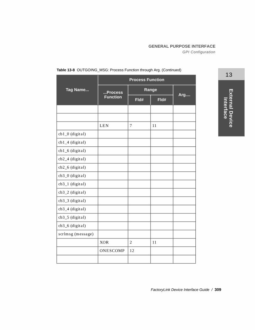
GENERAL PURPOSE INTERFACEGPI Configuration
FactoryLink Device Interface Guide / 309
13
Extern
al Device
Interface
LEN 7 11
cb1_0 (digital)
cb1_4 (digital)
cb1_6 (digital)
cb2_4 (digital)
cb2_6 (digital)
cb3_0 (digital)
cb3_1 (digital)
cb3_2 (digital)
cb3_3 (digital)
cb3_4 (digital)
cb3_5 (digital)
cb3_6 (digital)
scrlmsg (message)
XOR 2 11
ONESCOMP 12
Table 13-8 OUTGOING_MSG: Process Function through Arg. (Continued)
Tag Name...
Process Function
...ProcessFunction
RangeArg....
Fld# Fld#

GENERAL PURPOSE INTERFACEGPI Configuration
310 / FactoryLink Device Interface Guide
••••
stat_msg (message)
stat_ana (analog)
Table 13-9 OUTGOING_MSG: Conversion Function through Resp. LN, POS, TM
Tag Name...
Conversion Function Response
...ConversionFunction
FormatString
ResponseID
ResponseLN, POS, TM...
cb1_0 (digital)
cb1_4 (digital)
cb1_6 (digital)
cb2_4 (digital)
cb2_6 (digital)
Table 13-8 OUTGOING_MSG: Process Function through Arg. (Continued)
Tag Name...
Process Function
...ProcessFunction
RangeArg....
Fld# Fld#

GENERAL PURPOSE INTERFACEGPI Configuration
FactoryLink Device Interface Guide / 311
13
Extern
al Device
Interface
cb3_0 (digital)
cb3_1 (digital)
cb3_2 (digital)
cb3_3 (digital)
cb3_4 (digital)
cb3_5 (digital)
cb3_6 (digital)
scrlmsg (message)
2
111
stat_msg (message)
stat_ana (analog)
Table 13-10 OUTGOING_MSG: Response Packets through Comment
Tag Name...
Response Command/Response
Comment...Response
PacketsConstantNumeric
ConstantString
170 Hex AA
CMD Length
Table 13-9 OUTGOING_MSG: Conversion Function through Resp. LN, POS, TM (Continued)
Tag Name...
Conversion Function Response
...ConversionFunction
FormatString
ResponseID
ResponseLN, POS, TM...

GENERAL PURPOSE INTERFACEGPI Configuration
312 / FactoryLink Device Interface Guide
••••
16 Unit Addr
2 Unit Addr
2 Msg Len
1 Ctrl
Msg Len
cb1_0 (digital) Ctrl Byte 1
cb1_4 (digital) Ctrl Byte 1
cb1_6 (digital) Cntrl Byte 1
cb2_4 (digital) Ctrl Byte 2
cb2_6 (digital) Ctrl Byte 2
cb3_0 (digital) Ctrl Byte 3
cb3_1 (digital) Ctrl Byte 3
cb3_2 (digital) Ctrl Byte 3
cb3_3 (digital) Ctrl Byte 3
cb3_4 (digital) Ctrl Byte 3
cb3_5 (digital) Ctrl Byte 3
cb3_6 (digital) Ctrl Byte 3
scrlmsg (message) Scroll Message
Exclusive-Or
One’s Complement
Table 13-10 OUTGOING_MSG: Response Packets through Comment (Continued)
Tag Name...
Response Command/Response
Comment...Response
PacketsConstantNumeric
ConstantString

GENERAL PURPOSE INTERFACEGPI Configuration
FactoryLink Device Interface Guide / 313
13
Extern
al Device
Interface
Entries for Incoming Response Table
The following series of tables lists sample Command/Response Information panel entries for an incoming response table, INCOMING_RSP, that defines parameters for the various types of expected PMD 300 replies to the outgoing message defined in OUTGOING_MSG.
sngl_rsp Response Variable
Response ID
stat_msg (message) Status - Message
stat_ana (analog) Status - Analog
Table 13-11 INCOMING_RSP: Tag Name through Bit Pos.
Tag Name
FieldBit
Pos....FieldType
FieldPos.
FieldLen.
NUMERIC 1 1
length TAGVALUE 2 1
uaddr TAGVALUE 3 2
NUMERIC 4 1
reply TAGVALUE 5 1
error TAGVALUE 6 1
cksum TAGVALUE 7 2
Table 13-10 OUTGOING_MSG: Response Packets through Comment (Continued)
Tag Name...
Response Command/Response
Comment...Response
PacketsConstantNumeric
ConstantString
INCOMING_RSP

GENERAL PURPOSE INTERFACEGPI Configuration
314 / FactoryLink Device Interface Guide
••••
RESP_ID
astring STAT_TAG
mstring STAT_TAG
Table 13-12 INCOMING_RSP: Process Function through Arg.
Tag Name...
Process Function
...ProcessFunction
RangeArg....
Fld# Fld#
length
uaddr
reply
error
cksum
astring
mstring
Table 13-11 INCOMING_RSP: Tag Name through Bit Pos. (Continued)
Tag Name
FieldBit
Pos....FieldType
FieldPos.
FieldLen.

GENERAL PURPOSE INTERFACEGPI Configuration
FactoryLink Device Interface Guide / 315
13
Extern
al Device
Interface
Table 13-13 INCOMING_RSP: Conversion Function through Response LN, POS, TM
Tag Name...
Conversion Function Response
...ConversionFunction
FormatString
ResponseID
ResponseLN, POS, TM...
length
uaddr HI-LOW16
reply
error
cksum HI-LOW16
astring
mstring
Table 13-14 INCOMING_RSP: Response Packets through Comment
Tag Name...
Response Command/Response
Comment...Response
PacketsConstantNumeric
ConstantString
170 Hex AA
length Length
uaddr Unit Address
0 Place Holder (Delimiter)
reply Reply Code

GENERAL PURPOSE INTERFACEGPI Configuration
316 / FactoryLink Device Interface Guide
••••
Defining the Outgoing Message to the GPI
The field entries described below are for the sample GPI configuration:
1 One-byte numeric constant with a value of 170 (Hex AA).
2 Size equals the length of the entire outgoing message except for the first byte (Hex AA). The process function LEN calculates the number of bytes in Fields 2 - 13 (inclusive). Use the result of the calculation as the value of the second field of the outgoing message.
3, 4, 5, 6 One-byte numeric types whose values you know at configuration: enter their corresponding values in the Constant Numeric column.
7 The length of the string to be displayed on the device plus the number of control bytes. Three control bytes occupy fields 8, 9, and 10. The LEN process function calculates the number of bytes of fields 7 - 11 (inclusive). The result is the value of Byte 7.
error Error Code
cksum Error Checking
Response ID
astring Analog Status Tag
mstring Analog Status Tag
Table 13-14 INCOMING_RSP: Response Packets through Comment (Continued)
Tag Name...
Response Command/Response
Comment...Response
PacketsConstantNumeric
ConstantString

GENERAL PURPOSE INTERFACEGPI Configuration
FactoryLink Device Interface Guide / 317
13
Extern
al Device
Interface
8, 9, 10 These are control bytes. The PMD 300 customizes the string displayed on its screen using the value of these control bytes. The FactoryLink application controls the PMD device’s capabilities by linking various digital elements (up to eight per byte) to individual bits of these control bytes. This provides much flexibility at the application level.
This example defines the digital elements in the following manner:
The FactoryLink application links three digital elements—CB1_0, CB1_4, and CB1_6—to bits 1, 5, and 7 of field 8 (control byte 1).
The FactoryLink links two digital elements—CB2_4 and CB2_6—to bits 5 and 7 of Field 9 (control byte 2). (Field 7 in this example is the second control byte for the PMD 300 protocol.)
The FactoryLink application links seven digital elements—cb3_0, CB3_1, CB3_2, CB3_3, CB3_4, CB3_5, and CB3_6—to field 3 (control byte 3).
11 TAGVALUE. The FactoryLink message element SCRLMSG, which is 56 bytes long and linked to field 11, contains the string that the PMD 300 will display on screen.
12, 13 Process functions that calculate the checksum using the PMD 300 protocol. Field 12 is the exclusive-or (XOR) of all the bytes from fields 2 - 11 (inclusive); therefore, use process function XOR on this range of fields. Field 13 is the one's complement of the previous field.
The following three entries for the sample GPI configuration do not require field positions:
RESP_ID The unique response ID is 111.
RESP_VAR Single packet response; length is the second byte of the response data.
STAT_TAG FactoryLink message element STAT_MSG and analog element STAT_ANA.

GENERAL PURPOSE INTERFACEGPI Configuration
318 / FactoryLink Device Interface Guide
••••
Defining Response Termination and Status Elements
The PMD 300 example illustrates how to define response termination and status elements. The GPI protocol module then relays this status/error information about the outgoing message which is transmitted to the device.
In the Field Type column of the PMD 300 GPI Command/Response table, the single-packet response, SNGL_RSP, specifies a variable-length response. According to the PMD 300 protocol, the second byte of the response specifies the length of the response. For the GPI protocol module to detect the end-of-response, enter a 2 (for the second byte) in the Response LN, POS, TM column. The number of bytes in the response begins with third byte.
In the Response Packet column, the single-packet response SNGL_RSP is an example of a common response.
The next line in the table matches the response to the response format required by the outgoing message with the unique response ID, 111.
The last two lines of the table define FactoryLink analog and message elements. This allows the GPI protocol module to report the status of the outgoing message to the FactoryLink application.

GENERAL PURPOSE INTERFACEGPI Configuration
FactoryLink Device Interface Guide / 319
13
Extern
al Device
Interface
Defining the Incoming Response to the GPI
The following field entries describe the sample GPI configuration:
1 One-byte numeric constant with a value of 170 (hexadecimal value AA)
2 One-byte length of the incoming message stored in a FactoryLink analog element
3 Two-byte unit address received in HILOW format
4 One-byte numeric place holder (delimiter)
5 One-byte reply code that will be stored in a FactoryLink analog element
6 One-byte error code that will be stored in a FactoryLink analog element
7 Two-byte checksum received in HILOW format that will be stored in a FactoryLink analog element
The following entries do not require field positions:
RESP_ID The unique response ID is 111
STAT_TAG FactoryLink elements ASTRING and MSTRING

GENERAL PURPOSE INTERFACEUsing Process Functions
320 / FactoryLink Device Interface Guide
••••
USING PROCESS FUNCTIONS
This section contains information about the process functions to use with the GPI protocol module.
Depending on their functionality, process functions perform various operations on entries in the GPI tables. To produce the desired value, you enter a specific process function in the FLD# and Arg columns.
Process Functions Table
The table below describes operations of each process function:
Note
For the Field Type PROCESS, the Field Length can only be 1 or 2 bytes. Also, if a PROCESS FUNCTION has entries in the FLD# or Arg columns, then, depending on the value specified in the Field Length, it is a “char” (1-byte) or a “short” (2-bytes).
Table 13-15 Process Function Operations
Name Use Description
ADD ADD Arg ADDS the value given in Arg to the present value of the current field.
AM AM Arg AND MASKS (AM) the value of the current field with the value in Arg.
AND AND, FLD# Bit-wise AND operation on FLD#.
CRCCCITT CRCCCITT FLD#, Arg Computes the CRC of the specified range using a CRC_SEED=0x1021 (inclusive). Uses Arg to set the initial value.
CRCCC_RV CRCCC_RV FLD#, Arg Computes the CRC of the specified range using a CRC_SEED=0x8408 (inclusive). Uses Arg to set the initial value.
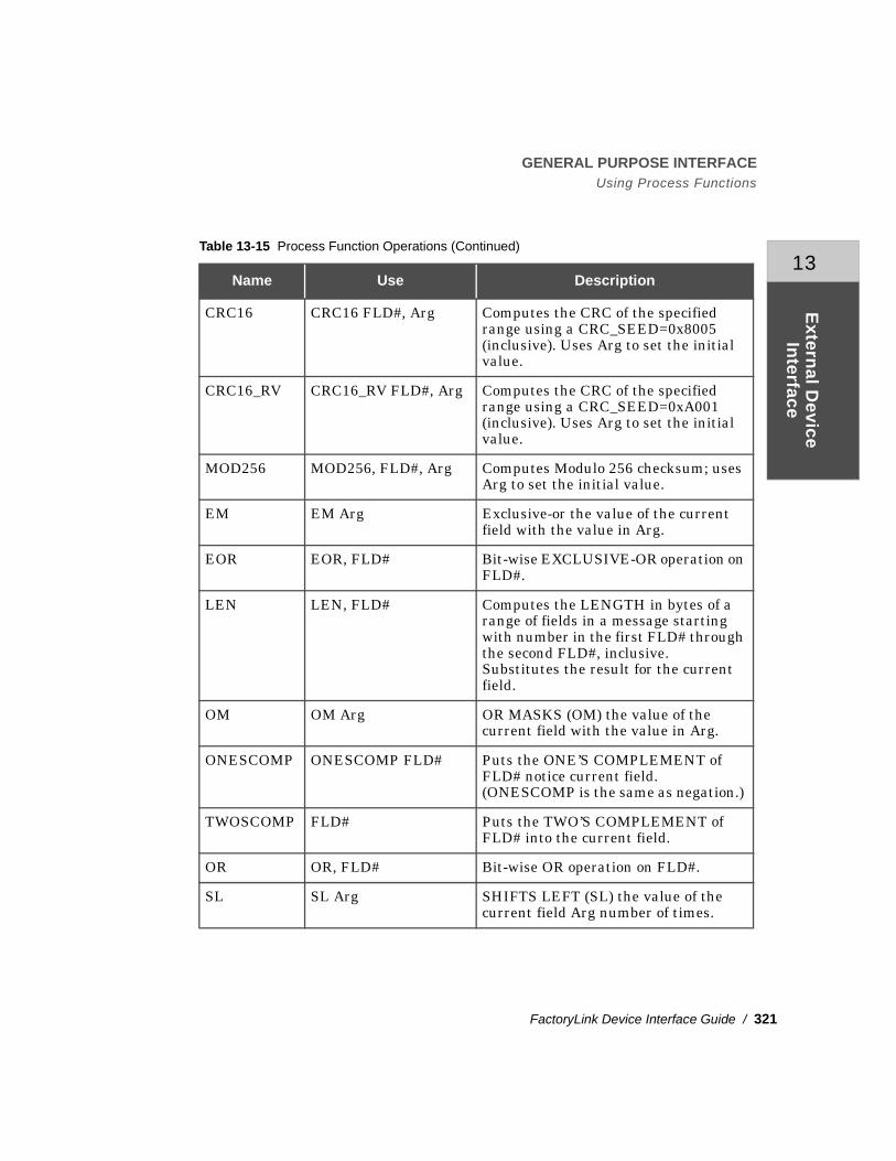
GENERAL PURPOSE INTERFACEUsing Process Functions
FactoryLink Device Interface Guide / 321
13
Extern
al Device
Interface
CRC16 CRC16 FLD#, Arg Computes the CRC of the specified range using a CRC_SEED=0x8005 (inclusive). Uses Arg to set the initial value.
CRC16_RV CRC16_RV FLD#, Arg Computes the CRC of the specified range using a CRC_SEED=0xA001 (inclusive). Uses Arg to set the initial value.
MOD256 MOD256, FLD#, Arg Computes Modulo 256 checksum; uses Arg to set the initial value.
EM EM Arg Exclusive-or the value of the current field with the value in Arg.
EOR EOR, FLD# Bit-wise EXCLUSIVE-OR operation on FLD#.
LEN LEN, FLD# Computes the LENGTH in bytes of a range of fields in a message starting with number in the first FLD# through the second FLD#, inclusive. Substitutes the result for the current field.
OM OM Arg OR MASKS (OM) the value of the current field with the value in Arg.
ONESCOMP ONESCOMP FLD# Puts the ONE’S COMPLEMENT of FLD# notice current field. (ONESCOMP is the same as negation.)
TWOSCOMP FLD# Puts the TWO’S COMPLEMENT of FLD# into the current field.
OR OR, FLD# Bit-wise OR operation on FLD#.
SL SL Arg SHIFTS LEFT (SL) the value of the current field Arg number of times.
Table 13-15 Process Function Operations (Continued)
Name Use Description

GENERAL PURPOSE INTERFACEUsing Process Functions
322 / FactoryLink Device Interface Guide
••••
SR R Arg SHIFTS RIGHT (SR) the value of the current field Arg number of times.
SUB SUB Arg SUBtracts the value given in Arg from the present value of the current field.
SWAP SWAP SWAPs the two consecutive bytes in the current field.
XOR XOR, FLD# Computes the EXCLUSIVE-Or of the range of bytes between FLD#, inclusive, and substitutes the result for the current field.
Table 13-15 Process Function Operations (Continued)
Name Use Description
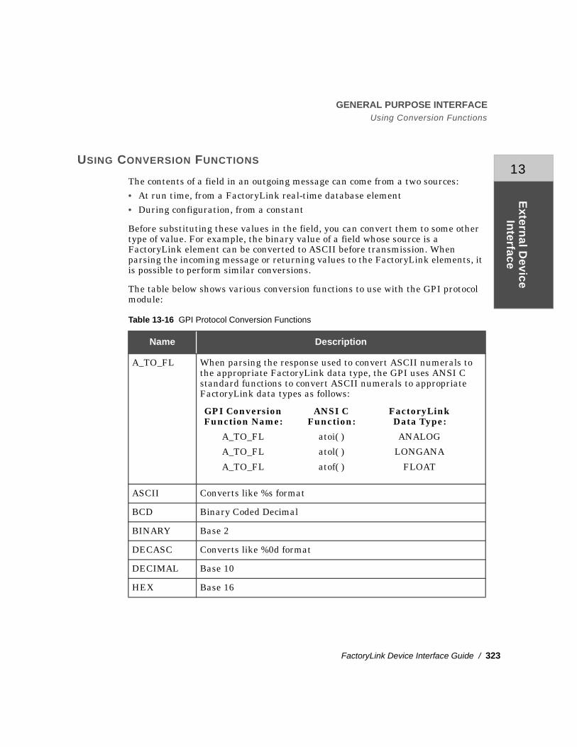
GENERAL PURPOSE INTERFACEUsing Conversion Functions
FactoryLink Device Interface Guide / 323
13
Extern
al Device
Interface
USING CONVERSION FUNCTIONS
The contents of a field in an outgoing message can come from a two sources:• At run time, from a FactoryLink real-time database element • During configuration, from a constant
Before substituting these values in the field, you can convert them to some other type of value. For example, the binary value of a field whose source is a FactoryLink element can be converted to ASCII before transmission. When parsing the incoming message or returning values to the FactoryLink elements, it is possible to perform similar conversions.
The table below shows various conversion functions to use with the GPI protocol module:
Table 13-16 GPI Protocol Conversion Functions
Name Description
A_TO_FL When parsing the response used to convert ASCII numerals to the appropriate FactoryLink data type, the GPI uses ANSI C standard functions to convert ASCII numerals to appropriate FactoryLink data types as follows:
ASCII Converts like %s format
BCD Binary Coded Decimal
BINARY Base 2
DECASC Converts like %0d format
DECIMAL Base 10
HEX Base 16
GPI Conversion Function Name:
ANSI C Function:
FactoryLink Data Type:
A_TO_FL atoi( ) ANALOG
A_TO_FL atol( ) LONGANA
A_TO_FL atof( ) FLOAT

GENERAL PURPOSE INTERFACEUsing Conversion Functions
324 / FactoryLink Device Interface Guide
••••
HEXASC Converts like %0x format
HILOW16 Converts to a 2-byte MSB LSB
HILOW32 Converts to a 4-byte MSW LSW
IEEEHL4 Converts to a 4-byte IEEE MSW LSW
IEEELH4 Converts to a 4-byte IEEE LSW MSW
IEEEHL8 Converts to an 8-byte IEEE MSDW LSDW
IEEELH8 Converts to an 8-byte IEEE LSDW MSDW
LOWHI16 Converts to a 2-byte LSB MSB
LOWHI32 Converts to a 4-byte LSW MSW
MBUSFLOT Converts to a Modicon float formatwhere:LSB is the least-significant byte.MSB is the most-significant byte.LSW is the least-significant word.MSW is the most-significant word.LSDW is the least-significant double word.MSDW is the most-significant double word.Word is a 2-byte entity.Double Word is a 4-byte entity.
NONE No conversion necessary
OCTASC Converts like %0 format
Table 13-16 GPI Protocol Conversion Functions (Continued)
Name Description

GENERAL PURPOSE INTERFACEUsing Conversion Functions
FactoryLink Device Interface Guide / 325
13
Extern
al Device
Interface
TSPRINTF Converts according to the explicit format given in the Format String column; the TSPRINTF function is a “tiny” sprintf( ) that handles %s, %d, %u, %x, %0, %lu, %lx, %lX, %l0, and %%. It recognizes width and pad specifications (%3d, %03d, etc.), long values, and left or right justification. Is tiny sprintf() correct?
Note: Because the TSPRINTF function does not recognize floating point formats (%e, %f, %g) and minimum widths, use it with FactoryLink Analog, Longana, and Message types with the appropriate format string.
Table 13-16 GPI Protocol Conversion Functions (Continued)
Name Description

GENERAL PURPOSE INTERFACESample Protocols
326 / FactoryLink Device Interface Guide
••••
SAMPLE PROTOCOLS
This section provides sample protocols that illustrate the format of various messages and responses. Use these as examples of protocols and not in your specific application.
Response Protocols
Field 1 (1 byte) PreambleConstant value
Field 2 (2 byte) PLC device addressConstant value
Field 3 (2 byte) Response charsConstant value or FactoryLink analog element
Field 4 (2 byte) Response header charsdConstant value or FactoryLink analog element
Field 5 (2 byte) Frame check sequencePROCESS
Field 6 (1 byte) Command terminatorConstant value
Field 7 (1 byte) PostambleConstant value
RESP_ID 101
RESP_STR Constant value “CR”
Table 13-17 Sample Outgoing Message, Request Protocol
Field 1 Field 2 Field 3 Field 4 Field 5 Field 6 Field 7
@ 0001 xxxx xxxx FCS * CR

GENERAL PURPOSE INTERFACESample Protocols
FactoryLink Device Interface Guide / 327
13
Extern
al Device
Interface
Field 1 (1 byte) PreambleConstant value
Field 2 (2 byte) PLC device addressConstant value
Field 3 (2 byte) Response charsFactoryLink analog element
Field 4 (2 byte) Response header charsFactoryLink analog element
Field 5 (2 byte) Frame check sequenceFactoryLink analog, digital, or float element
Field 6 (1 byte) FCS Checksum codesConstant value (Optional)
Field 7 (1 byte) Command terminator Constant value (Optional)
Field 8 (1 byte) Postamble Constant value (Optional)
RESP_ID 101
Table 13-18 Sample Incoming Response, Response Protocol
Field 1 Field 2 Field 3 Field 4 Field 5 Field 6 Field 7 Field 8
# 0001 xxxx xxxx xxxx FCS * CR

GENERAL PURPOSE INTERFACESample Protocols
328 / FactoryLink Device Interface Guide
••••
Command Protocols
Field 1 (1 byte) PreambleConstant value
Field 2 (2 byte) PLC device addressConstant value
Field 3 (2 byte) Command charsConstant value or FactoryLink analog element
Field 4 (2 byte) Command header charsConstant value or FactoryLink analog element
Field 5 (?-byte) Command dataFactoryLink analog, digital, or float elements
Field 6 (2 byte) Frame check sequenceProcess function
Field 7 (1 byte) Command terminatorConstant value
Field 8 (1 byte) PostambleConstant value
RESP_ID 222
RESP_FXD Length of 11 bytes constant value
Table 13-19 Sample Outgoing Message, Request Protocol
Field 1 Field 2 Field 3 Field 4 Field 5 Field 6 Field 7 Field 8
@ 0001 xxxx xxxx xxxx FCS * CR

GENERAL PURPOSE INTERFACESample Protocols
FactoryLink Device Interface Guide / 329
13
Extern
al Device
Interface
Field 1 (1 byte) PreambleConstant value
Field 2 (2 byte) PLC device addressConstant value
Field 3 (2 byte) Response charsFactoryLink analog element
Field 4 (2 byte) Response header charsFactoryLink analog element
Field 5 (2 byte) Frame check sequenceConstant value (Optional)
Field 6 (1 byte) Response terminatorConstant value (Optional)
Field 7 (1 byte) PostambleConstant value (Optional)
RESP_ID 222
Table 13-20 Sample Incoming Response, Response Protocol
Field 1 Field 2 Field 3 Field 4 Field 5 Field 6 Field 7
# 0001 xxxx xxxx FCS * CR

GENERAL PURPOSE INTERFACESample Protocols
330 / FactoryLink Device Interface Guide
••••
Network Response Protocols
Field 1 (1 byte) PreambleConstant value
Field 2 (2 byte) Length of network commandConstant value
Field 3 (1 byte) Network send data commandConstant value
Field 4 (1 byte) Secondary network addressConstant value
Field 5 (2 byte) Response length Constant value
Field 6 (1 byte) Response codeConstant value
Field 7 (1 byte) Response memory type Constant value
Field 8 (1 byte) # of data elementsConstant value
Field 9 (?-byte) Address of response dataConstant value
Field 10 (2 byte) Checksum codesProcess function
Field 11 (1 byte) PostambleConstant value (Optional)
RESP_ID 1
RESP_STR Constant string (;)
Table 13-21 Sample Outgoing Message, Request Protocol
Field 1
Field 2
Field 3
Field 4
Field 5
Field 6
Field 7
Field 8
Field 9
Field 10
Field 11
: xxxx 01 xx 0006 20 xx xxxx xxxx xxxx ;

GENERAL PURPOSE INTERFACESample Protocols
FactoryLink Device Interface Guide / 331
13
Extern
al Device
InterfaceField 1 (1 byte) Preamble
Constant value
Field 2 (2 byte) Length of network commandConstant value
Field 3 (1 byte) Network send data commandConstant value
Field 4 (1 byte) Secondary network addressConstant value
Field 5 (2 byte) Response length Constant value
Field 6 (1 byte) Response command codeConstant value
Field 7 (1 byte) Response memory type Constant value
Field 8 (1 byte) # of data elementsConstant value
Field 9 (?-byte) Response data from deviceFactoryLink analog, digital, or float element
Field 10 (2 byte) Checksum codesProcess function
Field 11 (1 byte) PostambleConstant value (Optional)
RESP_ID 1
Table 13-22 Sample Incoming Message, Response Protocol
Field 1
Field 2
Field 3
Field 4
Field 5
Field 6
Field 7
Field 8
Field 9
Field 10
Field 11
: xxxx 01 xx 0006 20 xx xxxx xxxx xxxx ;

GENERAL PURPOSE INTERFACESample Protocols
332 / FactoryLink Device Interface Guide
••••
Network Command Protocols
Field 1 (1 byte) PreambleConstant value
Field 2 (2 byte) Length of network commandConstant value
Field 3 (1 byte) Network send data commandConstant value
Field 4 (1 byte) Secondary network addressConstant value
Field 5 (2 byte) Command lengthConstant value
Field 6 (1 byte) Command codeConstant value
Field 7 (1 byte) Command memory type Constant value
Field 8 (1 byte) # of data elementsConstant value
Field 9 (?-byte) Command dataFactoryLink analog, digital, or float element(s)
Field 10 (2 byte) Checksum codesProcess function
Field 11 (1 byte) PostambleConstant value
RESP_ID 555
RESP_STR Constant string (;)
Table 13-23 Sample Outgoing Message, Request Protocol
Field 1
Field 2
Field 3
Field 4
Field 5
Field 6
Field 7
Field 8
Field 9
Field 10
Field 11
: xxxx 01 xx 0006 20 xx xxxx DDDD xxxx ;

GENERAL PURPOSE INTERFACESample Protocols
FactoryLink Device Interface Guide / 333
13
Extern
al Device
InterfaceField 1 (1 byte) Preamble
Constant value
Field 2 (2 byte) Length of network commandConstant value
Field 3 (1 byte) Network send data commandConstant value
Field 4 (1 byte) Secondary network addressConstant value
Field 5 (2 byte) Command length Constant value
Field 6 (1 byte) Command error codeFactoryLink analog or digital element
Field 7 (1 byte) Command codeConstant value (Place holder)
Field 8 (1 byte) Attached device statusFactoryLink analog element or digital element
Field 9 (1 byte) Device auxiliary power sourceFactoryLink analog or digital element
Field 10 (1 byte) NIM status codeFactoryLink analog or digital element
Field 11 (2 byte) Checksum codesFactoryLink analog (Optional)
Field 12 (1 byte) PostambleConstant value (Optional)
RESP_ID 555
Table 13-24 Sample Incoming Response, Response Protocol
Field 1
Field 2
Field 3
Field 4
Field 5
Field 6
Field 7
Field 8
Field 9
Field 10
Field 11
Field 12
: xxxx 01 xx 0005 xx 30 HH EE FF xxxx ;

GENERAL PURPOSE INTERFACERun-Time Application Messages
334 / FactoryLink Device Interface Guide
••••
RUN-TIME APPLICATION MESSAGES
During EDI run time, FactoryLink generates and displays messages for the General Purpose Interface protocol module on the Run-Time Manager screen and, if so configured, writes them to message or analog tags. For information about configuring these tags, see “Configuring the Logical Station Control Panel” on page 263 and “Configuring the Logical Station Information Panel” on page 267.
For information about the messages displayed for the EDI task and the format in which protocol module messages are generated, see Chapter 10, “Messages and Codes.”
GPI Error Codes
The remainder of this section describes the status/error codes written to FactoryLink analog and message elements and defined through the STAT_TAG feature of the GPI protocol module. The following are the formats for the GPI error codes:• The GPI reports a numeric code via FactoryLink analog elements. • The GPI reports an alphanumeric description via FactoryLink message
elements. • The GPI uses even-numbered codes as information or acknowledgment codes.• The GPI uses odd-numbered codes as error codes.• The GPI uses 1xx codes for making or transmitting the outgoing message.• The GPI uses 2xx codes for parsing the response.• The GPI uses 3xx codes for the logical port and reports them to the logical port
MSG STATUS elements. These codes apply to the operation of the logical port (the GPI protocol module) as a whole. They are not related to the individual transactions. At startup, the FactoryLink application checks their status.
1xx: Even-Numbered Information/Acknowledge Codes for Building/Transmitting the Outgoing Message
Table 13-25
Analog Message Element
100 asyndsf.c(DSF_WRITE): Start to make the cmnd
102 asyncpt(xmit) xmitED MSG SUCCESSFULLY

GENERAL PURPOSE INTERFACERun-Time Application Messages
FactoryLink Device Interface Guide / 335
13
Extern
al Device
Interface
1xx: Odd-Numbered Error Codes for Building/Transmitting the Outgoing Message
Table 13-26
Analog Message Element
101 ASYNDSF.C(DSF_WRITE): cmnd length of %d exceeds SND_BUF_LEN, FLD#%D
103 ASYNDSF.C(DSF_WRITE): Invalid FLD TYPE %d; FLD %d
105 ASYNDSF.C(DSF_WRITE): MAX_TERM_STR reached
107 ASYNDSF.C(DSF_WRITE): dsf_t_q_mail returned ERROR
109 ASYNDSF.C(GET_BUF_INX): Invalid INFO_TYPE=%D IN DIV_DEF
111 ASYNDSF.C(WRT_DO_STRING): Invld cnvr FUNC %D for STRING,fld #%d
113 ASYNDSF.C(WRT_DO_NUMERIC): Invld cnvr Func %d for NUMERIC, fld #%d
115 ASYNDSF.C(WRT_DO_PROCESS): Invld PROCESS Func %d, FLD #%D
117 ASYNDSF.C(WRT_DO_PROCESS): Invld cnvr FUNC%D for PROCESS, fld #%d
119 ASYNDSF.C(WRT_DO_PROCESS): Invld PROCESS Func %d, fld #%d
121 ASYNDSF.C(WRT_DO_PROCESS): Invld cnvr Func %d for PROCESS, FLD #%D
123 ASYNDSF.C(WRT_DO_PROCESS): Invld fld len%d for a PROC_FUNC FLD #%D
125 ASYNCPT(XMIT): xmit error

GENERAL PURPOSE INTERFACERun-Time Application Messages
336 / FactoryLink Device Interface Guide
••••
2xx: Even-Numbered Informative/Acknowledge Codes for Parsing the Response
2xx: Odd-Numbered Error Codes for Parsing the Response
Table 13-27
Analog Message Element
200 ASYNDSF.C(PROCESS_RESPONSE): Start to PROC RESP #%D
202 ASYNDSF.C(PROCESS_RESPONSE): MULT_RSP Completed
204 ASYNDSF.C(PROCESS_RESPONSE): ProcessED Resp ID# %d AOK
Table 13-28
Analog Message Element
201 ASYNDSF.C(PROCESS_RESPONSE): RSP_BUF too short %d
203 ASYNDSF.C(PROCESS_RESPONSE): inter char time out
205 ASYNDSF.C(PROCESS_RESPONSE): RSP_TM_OUT
207 ASYNDSF.C(PROCESS_RESPONSE): RESPONSE ERROR
209 ASYNDSF.C(MATCH_RSP): Invalid DIV-DS.INFO_TYPE=%D, RPS_ID =%D
211 ASYNDSF.C(GET_USL_BUF_INX): DLMTR FOR FLD #%D, RSP ID #%D, not found
213 ASYNDSF.C(GET_USL_BUF_INX): End of RSP_BUF reached INX %D, FLD #%D, RSP ID #%D
215 ASYNDSF.C(GET_USL_BUF_INX): DLMTR FOR FLD # %D, RSP ID #%D, not found
217 ASYNDSF.C(GET_USL_BUF_INX): End of RSP_BUF REACHED, INX%D, FLD #%D, RSP ID #%D
219 ASYNDSF.C(RD_DO_TAGVALUE): Fld. Len. Exceeded 255; RESP #%D

GENERAL PURPOSE INTERFACERun-Time Application Messages
FactoryLink Device Interface Guide / 337
13
Extern
al Device
Interface
221 ASYNDSF.C(RD_DO_TAGVALUE): Invalid CNVR for digital; FLD# %D
223 ASYNDSF.C(RD_DO_TAGVALUE): Invalid cnvr for analog; FLD# %D
225 ASYNDSF.C(RD_DO_TAGVALUE): Invalid cnvr for lanalog; FLD# %D
227 ASYNDSF(RD_DO_TAGVALUE): Invalid cnvr for float; FLD# %D
229 ASYNDSF.C(RD_DO_TAGVALUE): Invalid cnvr for MESSAGE Tag; FLD#%D
231 ASYNDSF.C(RD_DO_TAGVALUE): Invalid fl_type%d for FLD# %D
233 ASYNDSF.C(RD_DO_STRING): STRING; Parser failed FLD# %D
235 ASYNDSF.C(RD_DO_NUMERIC): NUMERIC, Parser failed, FLD# %D
237 ASYNDSF.C(RD_DO_RAWVALUE): Fld. Len. Exceeded 255; Resp #%d
239 ASYNDSF.C(RD_DO_RAWVALUE): Invalid cnvr for MESSAGE Tag fld#%d
241 ASYNDSF.C(RD_DO_RAWVALUE): Invalid FL_TYPE %d for RAWVALUE
243 ASYNDSF.C(PROCESS_RESPONSE): USL_TM_OUT
Table 13-28 (Continued)
Analog Message Element

GENERAL PURPOSE INTERFACERun-Time Application Messages
338 / FactoryLink Device Interface Guide
••••
3xx: Even-Numbered Informative/Acknowledge Codes for the Logical Port
3xx: Odd-Numbered Error Codes for the Logical Port
Table 13-29
Analog Message Element
302 ASYNDSF.C(ALLOC_MEM_ON_ARTIC): AllocED %d bytes on ARTIC for SND bufr
304 ASYNDSF.C(ALLOC_MEM_ON_ARTIC): AllocED %d bytes on Artic for RCV BUFR
306 ASYNDSF.C(ALLOC_MEM_ON_SU): ALLOCED %D bytes for SND BUFR
308 ASYNDSF.C(ALLOC_MEM_ON_SU): ALLOCED %D bytes for RCV BUFR
310 ASYNDSF.C(FREE_MEM_ON_SU): freed mem for send and RCV BUFRS
314 ASYNDSF.C (DSF_START): PORT_SETUP_AOK
Table 13-30
Analog Message Element
301 ASYNDSF.C(ALLOC_MEM_ON_ARTIC): Unable to alloc mem on Artic for SND BUFR %D bytes
303 ASYNDSF.C(ALLOC_MEM_ON_ARTIC): Unable to alloc mem on ARTIC for RCV BUFR %D bytes
305 ASYNDSF.C(ALLOC_MEM_ON_SU): Unable to alloc mem for SND BUFR
307 ASYNDSF.C(ALLOC_MEM_ON_SU): Unable to alloc mem for RCV BUFR
311 ASYNCPT.C(CPT_START): Protection bit failure (ASYNCPT)
313 ASYNCPT.C(CPT_START): PORT_SETUP failed%04Xh

GENERAL PURPOSE INTERFACERun-Time Application Messages
FactoryLink Device Interface Guide / 339
13
Extern
al Device
Interface
315 ASYNCPT.C(CPT_TSLICE): unknown state: %d
317 ASYNCPT.C(XMIT): xmit error
319 ASYNCPT.C(XMIT): CPT_SND_USL returned: %04XH
321 ASYNCPT.C(XMIT): INVALID PKT_TYPE: %04XH
323 ASYNCPT.C(RCV_CK_RSP_TM): receive character error %04XH
325 ASYNCPT.C(RCV_CK_RSP_TM): USL_TM_OUT error
327 ASYNCPT.C(RCV_CK_RSP_TM): RSP_TM_OUT error
329 ASYNCPT.C(RCV_CHAR): receive character error %04Xh
331 ASYNCPT.C(RCV_CHAR): ICH_TM_OUT error
333 ASYNCPT.C(RCV_CHAR): TOTAL_TM_OUT reached
335 ASYNCPT.C(RCV_RSP_TM): TOTAL_TM_OUT reached
337 ASYNCPT.C(RCV_FINITO): CPT_SND_USL returned: %04XH
Table 13-30 (Continued)
Analog Message Element

GENERAL PURPOSE INTERFACERun-Time Application Messages
340 / FactoryLink Device Interface Guide
••••

Mo
dico
n M
od
bu
s
FactoryLink Device Interface Guide / 341
14
Extern
al Device
Interface
• • • •Chapter 14
Modicon Modbus
This chapter contains information needed to set up and configure bidirectional communications between the FactoryLink real-time database and any Modicon Modbus PLC.
When you choose Modicon Modbus from the Configuration Manager Main Menu, the Modicon Modbus configuration panels are displayed.
Note
Before completing the protocol-specific Modicon Modbus configuration panels, you must complete the External Device Definition panel. See “Identifying Protocol Types and Defining Logical Ports” on page 70 for details.

342 / FactoryLink Device Interface Guide
••••
MODICON MODBUSConfiguring the Logical Station Control Panel
CONFIGURING THE LOGICAL STATION CONTROL PANEL
To bring the Logical Station Control panel to the foreground, click its title bar in the display of all configuration panels.
Complete a row for each logical port specified in the External Device Definition panel you want to define as a communication path for read and write operations.
Logical Port Enter a number, defined in the External Device Definition panel Logical Port column, to represent a particular communication path to a Modicon Modbus device.
Valid Entry: previously defined logical port number
Baud Rate Enter the speed at which the protocol module communicates with the devices linked to FactoryLink via this logical port. This entry must match the baud rate configuration of the devices. Refer to the device manufacturer ’s documentation for details.
Valid Entry: 110 - 115200 (default=9600)
Parity Enter the parity error correction during transmission via this logical port. This entry must match the configuration of the devices communicating via this port. Refer to the device manufacturer’s documentation for details.
Valid Entry: none, even, or odd (default=odd)

FactoryLink Device Interface Guide / 343
Mo
dico
n M
od
bu
s
14
Extern
al Device
Interface
MODICON MODBUSConfiguring the Logical Station Control Panel
Data Bits Enter the number of data bits used during transmission via this logical port. This entry must match the configuration of the devices communicating via this port. Refer to the device manufacturer’s documentation for details.
Valid Entry: 7, 8 (default=8)
Stop Bits Enter the number of bits sent after a character to create a pause before the start of the next character. This entry must match the configuration of the devices communicating via this port. Refer to the device manufacturer ’s documentation for details.
Valid Entry: 1, 2 (default=1)
Timeout Enter the length of time, in tenths of a second, the protocol module will wait to receive a response to a read or write command before timing out. You must enter a value greater than 0 for the protocol module to timeout.
Valid Entry: 1 - 32000 (default=30)
RTU ASCII Enter the communication mode for this logical port.
Valid Entry: RTU, ASCII (default=RTU)
Message Tag Enter a tag name for a message element to which a text string will be written to indicate a communications error associated with this logical port.
Valid Entry: standard element tag nameValid Data Type: message
When the panel is complete, click Enter to validate the information. Define the data type (message) for any tag names displayed in the Tag Definition dialog.

344 / FactoryLink Device Interface Guide
••••
MODICON MODBUSConfiguring the Logical Station Information Panel
CONFIGURING THE LOGICAL STATION INFORMATION PANEL
From the Logical Station Control panel, select the row for the logical port you are configuring and click Next to bring the Logical Station Information panel to the foreground.
Complete a row for each device to communicate through this logical port.
Error/Status TagName
(Optional) Enter a tag name for an analog element in which to store communications error codes associated with this device (logical station).
You can animate output-text objects to display the codes stored in an Error/Status Tag Name element on a graphics screen. Refer to the Application Editor User Guide for more information.
Valid Entry: standard element tag nameValid Data Type: analog

FactoryLink Device Interface Guide / 345
Mo
dico
n M
od
bu
s
14
Extern
al Device
Interface
MODICON MODBUSConfiguring the Logical Station Information Panel
Logical Station Enter a number to identify the logical station to which the information in this row pertains. A logical station represents the combination of a logical port with a physical station. Assign a unique number to each device communicating through this logical port.
You will later enter this logical station number in a read or write table to represent the device defined in this row. In a read or write table, this number will identify the device to or from which data is to be sent or received.
Valid Entry: 0 - 999
Device Type Enter the type of Modicon device represented by this entry. The following table lists the valid entries and their variations. You can specify any of the valid entry variations in this field.
Station Address Enter the physical address of the Modicon device represented by this entry.
Valid Entry: 1 - 24 (default=1)
Comment (Optional) Enter reference information about this logical station.
Valid Entry: 1 - 31
When the panel is complete, click Enter to validate the information. Define the data type (analog) for any tag names displayed in the Tag Definition dialog.
Valid Entry Variation
184 184, 1, or 18
384 384, 3, or 38
484 484, 4, or 48
584 584, 5, or 58
884 884, 8, or 88
984 984, 9, or 98
984BITWRITE (Used for mask writes)
984-BW
M84 (Micro84) M84, M, or M8

346 / FactoryLink Device Interface Guide
••••
MODICON MODBUSConfiguring the Read/Write Control Panel
CONFIGURING THE READ/WRITE CONTROL PANEL
To bring the Read/Write Control panel to the foreground, click its title bar in the display of all configuration panels or click Next from the Logical Station Information panel.
A read or write table should not contain more than the maximum number of contiguous registers allowed for a single message accessing a type of register. The maximum number allowed varies from one register type to the next.
If more than the maximum number of contiguous register addresses are defined, multiple messages are generated for the operation. For example, if a block read table for a holding register contains entries that access contiguous addresses from 100 to 127, two messages are generated. The first message reads the first 125 addresses (addresses 100 to 124). The second message reads addresses 125 through 127.
The following table lists the maximum number of contiguous registers included in a single block read or write message for each supported register type.

FactoryLink Device Interface Guide / 347
Mo
dico
n M
od
bu
s
14
Extern
al Device
Interface
MODICON MODBUSConfiguring the Read/Write Control Panel
Table 14-1 Maximum Contiguous Registers in a Single Message
Type ofRegister
Modicon Model Number
Maximum NumberFor Block Read
Maximum NumberFor Block Write
Coil 184, 384 800 800
484 512 800
584, 884, 984 2000 800
M84 64 64
Holding 184, 384 100 100
484 254 60
584, 884, 984 125 100
M84 32 32
Input Status 184, 384 800
484 512
584, 884, 984 2000
M84 64
Input 184, 384 100
484 32
584, 884, 984 125
M84 4
Memory 100 100

348 / FactoryLink Device Interface Guide
••••
MODICON MODBUSConfiguring the Read/Write Control Panel
Complete a row for each read or write table.
Table Name Give this read or write request a name. Define one request (table) per line and do not include spaces in the name. You can define as many tables in this panel as available memory allows. Try to make the table name reflective of the operation it represents.
If this is a triggered read or a block write table, when the trigger element (Block Read Trigger for a read operation or Block Write Trigger for a write operation) is forced to 1 (ON), the element prompts FactoryLink to process this table and any other table in which the same trigger is defined.
Valid Entry: alphanumeric string of up to 16 characters
Exception Write For EDI to interpret this operation as a triggered block write or as a read operation, accept the default of NO.
For EDI to interpret this operation as an exception write and write element values to the device only when those values change, enter YES.
In an exception write, an internal change-status indicator within the element containing the data to be written prompts the write operation. If an element is configured for an exception write and EDI recognizes this indicator has been set since the last scan of the real-time database (indicating the value of the element has changed), EDI writes this element’s value to the device.
Tip
Refer to Chapter 8, “Application Design Tips and Techniques,” for information about triggering schemes using elements defined in this panel.
Tip
Do not specify elements expected to change at frequent and unpredictable intervals in an exception write table. Any element specified will be written to the device in its own packet (message) each time it changes. Defining elements that change value frequently as exception writes can slow down communications or result in an error message.

FactoryLink Device Interface Guide / 349
Mo
dico
n M
od
bu
s
14
Extern
al Device
Interface
MODICON MODBUSConfiguring the Read/Write Control Panel
Block Read Priority If this is a block read operation, enter a number to indicate the priority of this table, relative to other read operations. The highest priority is 1. This number influences the order in which the EDI task handles the queuing of block read requests. If EDI receives two requests at the same time, it processes the request with the highest priority first. The default is 1.
If this is a write operation, accept the default of 1. This field defaults to 1 regardless of whether the operation being defined is a block read.
Valid Entry: 1 - 4 (default=1)
Block Read Trigger If this is a write operation, ignore this field.
If this is a triggered read operation, this field is required. Enter a tag name for a digital element to initiate a block read of the addresses specified in the Read/Write Information panel. When this element’s value is forced to 1 (ON), the addresses are read.
Valid Entry: standard element tag nameValid Data Type: digital
Block ReadDisable
If this is a write operation, ignore this field.
If this is a triggered read operation, this field is optional. If you need a digital element to disable a block read of the elements specified in this table, enter a tag name. When this tag’s value is forced to 1 (ON), the read operation is not executed, even when the block read trigger is set to 1.
Note
The Block Read Trigger, Block Read Disable, Block Read Complete, and Block Read State elements apply only to triggered read operations. Do not define these elements for write operations.

350 / FactoryLink Device Interface Guide
••••
MODICON MODBUSConfiguring the Read/Write Control Panel
To re-enable a block read table that has been disabled, set this element back to 0 (OFF).
Valid Entry: standard element tag nameValid Data Type: digital
Block ReadComplete
If this is a write operation, ignore this field.
If this is a triggered read operation, this field is optional. If you need a digital element to indicate when this operation is complete, enter a tag name. This element is forced to 1 (ON) at startup. After the elements defined in the Read/Write Information panel have been updated in the FactoryLink database, the complete element is forced to 1 again.
Do not use this element when more than one logical port is specified in a single table.
Valid Entry: standard element tag nameValid Data Type: digital
Block Read State If this is a write operation, ignore this field.
If this is a triggered read operation, this field is optional. If you need a digital element to indicate the state of this operation (in progress or complete), enter a tag name. This element is forced to 1 (ON) at startup. While the table is being processed, the element is set to 0 (OFF). After the elements defined in the Read/Write Information panel have been updated in the FactoryLink database, the state element is forced back to 1.
Valid Entry: standard element tag nameValid Data Type: digital
Block Write Priority If this is a block or exception write operation, enter a number to indicate the priority of this table, relative to other write operations. The highest priority is 1. This number influences the
Tip
This element can be used to disable a block read operation that is either part of a cascaded loop or is self-triggered. The triggering cycle will cease upon disabling, however. To re-enable a cascaded loop or a self-triggered read table, the Block Read Trigger element must be toggled or forced to 1. Refer to Chapter 8, “Application Design Tips and Techniques,” for further details.

FactoryLink Device Interface Guide / 351
Mo
dico
n M
od
bu
s
14
Extern
al Device
Interface
MODICON MODBUSConfiguring the Read/Write Control Panel
order in which the EDI task handles the queuing of write requests. If EDI receives two requests at the same time, it processes the request with the highest priority first. The default is 1.
If this is a read operation, accept the default of 1. This field defaults to 1 regardless of whether the operation being defined is a block or exception write.
Valid Entry: 1 - 4 (default=1)
Block Write Trigger If this is a read operation or an exception write operation you do not plan to periodically disable, ignore this field.
If this is a block write table or an exception write table you plan to periodically disable, this field is required. Enter a tag name for a digital element to initiate a block write of the element values specified in the Read/Write Information panel to the addresses defined to receive the values. When this element’s value is forced to 1 (ON), FactoryLink writes the values.
Valid Entry: standard element tag nameValid Data Type: digital
Block WriteDisable
If this is a read operation or an exception write operation you do not plan to periodically disable, ignore this field.
Note
The Block Write Trigger, Block Write Disable, Block Write Complete, and Block Write State elements apply only to write operations. Do not define these elements for read operations.
Tip
The Block Write Disable element can be used to disable a block write operation that is either part of a cascaded loop or is self-triggered. The triggering cycle will cease upon disabling, however. To re-enable a cascaded loop or a self-triggered write table, the Block Write Trigger element must be toggled or forced to 1. Refer to Chapter 8, “Application Design Tips and Techniques,” for details.

352 / FactoryLink Device Interface Guide
••••
MODICON MODBUSConfiguring the Read/Write Control Panel
If this is a block write table or an exception write table you plan to periodically disable, this field is optional. Enter a tag name for a digital element to disable a block write to the addresses specified in this table. When this tag’s value is forced to 1 (ON), the write operation is not executed, even when the block write trigger is set to 1.
To re-enable a block write table that has been disabled, set this element back to 0 (OFF).
Valid Entry: standard element tag nameValid Data Type: digital
Block WriteComplete
If this is a read or exception write operation, ignore this field.
If this is a block write operation, this field is optional. If you need a digital element to indicate when this operation is complete, enter a tag name. This element is forced to 1 (ON) at startup. After the data defined in this table’s Read/Write Information panel has been written to the device, the complete element is forced to 1 again.
Do not use this element when more than one logical port is specified in a single table.
Valid Entry: standard element tag nameValid Data Type: digital
Block Write State If this is a read or exception write operation, ignore this field.
If this is a block write operation, this field is optional. If you need a digital element to indicate the state of this operation (in progress or complete), enter a tag name. This element is forced to 1 (ON) at startup. While the table is being processed, the element is set to 0 (OFF). After the data defined in this table’s Read/Write Information panel has been written to the device, the state element is forced back to 1.
Do not use this element when more than one logical port is specified in a single table.
Valid Entry: standard element tag nameValid Data Type: digital
When the panel is complete, click Enter to validate the information. Define the data type (digital) for any tag names displayed in the Tag Definition dialog.

FactoryLink Device Interface Guide / 353
Mo
dico
n M
od
bu
s
14
Extern
al Device
Interface
MODICON MODBUSConfiguring the Read/Write Information Panel
CONFIGURING THE READ/WRITE INFORMATION PANEL
From the Read/Write Control panel, select the row for the table you are configuring and click Next to bring the Read/Write Information panel to the foreground.
For a Read Table—Add a panel entry for each FactoryLink database element in which data read from the device will be stored when the operation executes.
For a Write Table—Add a panel entry for each element to be written when the operation executes.
Tag Name For a read table, specify a tag name for an element in which FactoryLink will store the data read from the device.
Tip
Alternatively, the elements you define in the Read/Write Information panel can be configured in the Tag Definition dialog in the Application Editor. Refer to the Application Editor User Guide for details.

354 / FactoryLink Device Interface Guide
••••
MODICON MODBUSConfiguring the Read/Write Information Panel
For a write table, specify a tag name for an element containing a value to be written to the device.
Logical Station Enter the number representing the device from which the data is to be read or to which the element’s value will be written. This number was originally defined in the Logical Station Information panel for the logical port through which communications with this device occurs.
Valid Entry: previously defined logical station number
Reg Address Enter the register address in Modicon memory where this element’s value is located. The format of a register address is:
paaaaa
where
p Address prefix that identifies the Modicon register type
Tag Type Element DescriptionValid for Register Types:
Analog A tag that stores a signed 16-bit integer with a value range between -32,768 and +32,767
HREGIREGXMEMnn
Digital A tag that stores a binary that indicates either a set (1) or unset (0) bit
COILHREGINPIREG
Float A tag that stores a floating-point integer with a value that can range up to 31 places to the right side of the decimal point
HREG
Longana A tag that stores a signed 32-bit integer with a value range between + or - 2 billion
HREG
Message A tag that stores ASCII text HREG

FactoryLink Device Interface Guide / 355
Mo
dico
n M
od
bu
s
14
Extern
al Device
Interface
MODICON MODBUSConfiguring the Read/Write Information Panel
aaaaa Actual address of the register
When defining register addresses, do not include the address prefix or leading zeros. The prefix indicates the register type, and this information is specified in the Data Type field of this panel. The leading zeros are extraneous.
For example, for holding register address 400001, enter 1. The 4 indicates the register type, and the leading zeros are not necessary.
If you are defining an address for floating-point or long analog tag types, keep in mind that these tag types are addressed in pairs. The first register in the pair contains the high-order word; the second register contains the low-order word.
Enter the address for the starting register in a register pair; the companion register is implied.
Try to maintain consistency when using register addresses for floating-point and long analog FactoryLink data types. Adopt either an odd or even starting register sequence and maintain that sequence. For example:
1, 3, 5, 7, 9, ...
or
2, 4, 6, 8, 10, ...
If you are defining an address for a message tag type, the address specifies the first in a group of registers that contain the message characters. The message length is specified in the Bit Offset/MSG Length field.
If you are reading or writing to extended memory, a block read, block write, or exception write operation may read or write multiple register addresses for the same register file.

356 / FactoryLink Device Interface Guide
••••
MODICON MODBUSConfiguring the Read/Write Information Panel
Bit Offset/MSGLength
This field is required for digital data type. If the element (entry in the Tag Name column) associated with this entry is digital, enter the bit offset within the word that contains the value to be read or to which the element value is to be written. Bit 1 is the most significant bit (MSB) and bit 16 is the least significant bit.
Leave this field blank for all other FactoryLink data types.
For digital tags that reference an address in memory from a holding register or input register (see Data Type field description), this is the bit offset between 1 and 16 within a register word that contains the value of the element. When defining this offset, follow Modicon’s convention for bit ordering, where bit 1 is the most significant bit (MSB) and bit 16 is the least significant bit (LSB).
For digital tags that reference mask write functions, use this field to indicate which bit between 1 and 16 will change in the register as a result of a mask write command. You can only address one bit per tag entry.
For message tags, this is the number of bytes in the device’s memory, between 1 and 80, containing the message. This number of bytes, starting from the location specified in the Address field of this panel, is read into the message tag as raw binary data. The FactoryLink Modbus Plus protocol module does not perform verification on these bytes to see if they are printable ASCII.
Valid Entry: 1 - 16 if data type is digital
Data Type Specify the type of data being read from or written to the device for each element defined in the Tag Name field.
1 2 3 4 5 6 7 8 9 10 11 12 13 14 15 16
MSB LSB
Data Type Valid Operations
COIL Block read operations read current value of the element.
Block write and exception write operations are used to force the state of coils to either on or off.

FactoryLink Device Interface Guide / 357
Mo
dico
n M
od
bu
s
14
Extern
al Device
Interface
MODICON MODBUSConfiguring the Read/Write Information Panel
When the panel is complete, click Enter to validate the information. Define the data type (digital, analog, long analog, or floating-point) for any tag names displayed in the Tag Definition dialog.
HREG Block read operations are used to get contents of a holding register.
Block write and exception write operations are used to set the contents of a holding register.
INP Block read operations read the ON/OFF status of discrete inputs. Input is stored in a controller as bits. Each bit has an address.
IREG Block read operations are used to read the binary contents of an input register.
MASK Exception write operations are used to set or clear bits within a holding register. The current state of the digital tag determines the ON/OFF setting of the bit within the holding register. To set a bit within the holding register, the digital tag must be set to 1(ON) and to clear a bit, it must be set to 0 (OFF).
XMEMnn Block read operations read the contents of extended memory.
Block write and exception write operations write to extended memory.
Data Type Valid Operations

MODICON MODBUSRun-Time Application Messages
358 / FactoryLink Device Interface Guide
••••
RUN-TIME APPLICATION MESSAGES
During EDI run time, FactoryLink generates and displays messages for the Modicon Modbus protocol module on the Run-Time Manager screen and, if so configured, writes them to message or analog tags. For information about configuring a message tag, see “Configuring the Logical Station Control Panel” on page 342. For information about configuring an analog tag, see “Configuring the Logical Station Information Panel” on page 344.
For information about the messages displayed for the EDI task, see Chapter 10, “Messages and Codes.”
Run-Time Manager Codes
The following error codes can appear in messages displayed on the Run-Time Manager screen. The first number refers to the hexadecimal code; the second number is its decimal equivalent.
1 (Decimal equivalent: 1)
Cause: Unknown I/O state.
Action: Verify the device configuration and cabling. The FactoryLink configuration tables must contain the proper station addresses and parameters. The Logical Station Control panel must contain the proper baud rate, parity, and data format parameters.
2 (Decimal equivalent: 2)
Cause: I/O error in transmitting or receiving data.
Action: Refer to the previous description of code 1.
3 (Decimal equivalent: 3)
Cause: I/O aborted because of a time-out while the protocol module is waiting for a device response.
Action: Refer to the description of code 1.
4 (Decimal equivalent: 4)
Cause: I/O data translation error.
Action: Refer to the description of code 1.

FactoryLink Device Interface Guide / 359
Mo
dico
n M
od
bu
s
14
Extern
al Device
Interface
MODICON MODBUSRun-Time Application Messages
15 (Decimal equivalent: 21)
Cause: Exception response—The slave cannot respond to the function code given in the query.
Action: Check the read and write tables and verify the data types are valid for the destination device.
25 (Decimal equivalent: 37)
Cause: Exception response—The data address received in the query by the device is not valid.
Action: Verify the register addresses in the table experiencing the error.
35 (Decimal equivalent: 53)
Cause: Exception response—An invalid data value in the query has been detected by the device.
Action: Depending on the data type of the table in error, verify each tag value is valid for the specified data type.
45 (Decimal equivalent: 69)
Cause: Exception response—The device has experienced an unrecoverable error while executing a requested action.
Action: Determine whether the device is in proper working order. It might require servicing.
55 (Decimal equivalent: 85)
Cause: Exception response—The device requires a long time to carry out the requested action.
Action: If the ladder logic programmed into the device is inefficient, it can result in time-consuming processing of requests. Reprogram the device according to the manufacturer’s recommendations.
65 (Decimal equivalent: 101)
Cause: Exception response—The device is busy carrying out a previously requested action.
Action: The device needs more time to finish processing the current request before it begins processing the next one. Lessen the frequency of requests sent to the device.

MODICON MODBUSRun-Time Application Messages
360 / FactoryLink Device Interface Guide
••••
75 (Decimal equivalent: 117)
Cause: Exception response—The device cannot perform the program function received in the query.
Action: Use the Modicon diagnostic software to determine the cause of the problem.
85 (Decimal equivalent: 113)
Cause: Exception response—The device attempted to read extended memory but detected a memory parity error.
Action: Determine whether the device is in proper working order. It might require servicing.
In Message Tags
This section describes the run-time messages as they appear in the message tags.
Modbus: Communications OK
Cause: Normal.
Action: None. This is only an information message.
Modbus: Exception error decimalcode on write to Lsta logical station
Cause: An error occurred on a write request to the specified logical station.
Action: The specified error is the decimal equivalent of a hexadecimal error code. For details, refer to “Run-Time Manager Codes” on page 358.
Modbus: Exception error decimalcode on read to Lsta logical station
Cause: An error occurred on a read request to the specified logical station.
Action: The specified error is the decimal equivalent of a hexadecimal error code. For details, refer to “Run-Time Manager Codes” on page 358.

FactoryLink Device Interface Guide / 361
Mo
dico
n M
od
bu
s
14
Extern
al Device
Interface
MODICON MODBUSRun-Time Application Messages
Modbus: Write error decimalcode to Lsta logical station
Cause: An error occurred on a write request to the specified logical station.
Action: The specified error is the decimal equivalent of a hexadecimal error code. For details, refer to “Run-Time Manager Codes” on page 358.
Modbus: Read error decimalcode to Lsta logical station
Cause: An error occurred on a read request to the specified logical station.
Action: The specified error is the decimal equivalent of a hexadecimal error code. For details, refer to “Run-Time Manager Codes” on page 358.

MODICON MODBUSRun-Time Application Messages
362 / FactoryLink Device Interface Guide
••••

FactoryLink Device Interface Guide / 363
15
Extern
al Device
Interface
• • • •
Mo
dico
n M
od
bu
s Plu
s
Chapter 15
Modicon Modbus Plus
The FactoryLink EDI task allows you to configure bidirectional communications between the FactoryLink real-time database and any Modicon Modbus Plus PLC.
When you choose Modicon Modbus Plus from the Configuration Manager Main Menu, the Modicon Modbus Plus configuration panels are displayed.
Sample panel entries are provided in Chapter 6, “Reading Data from a Device,” and Chapter 7, “Writing Data to a Device.”
Note
Before completing the protocol-specific Modicon Modbus Plus configuration panels, you must complete the External Device Definition panel. See “Identifying Protocol Types and Defining Logical Ports” on page 70 for details.

364 / FactoryLink Device Interface Guide
••••
MODICON MODBUS PLUSConfiguring the Logical Station Control Panel
CONFIGURING THE LOGICAL STATION CONTROL PANEL
To bring the Logical Station Control panel to the foreground, click its title bar in the display of all configuration panels.
Complete a row for each logical port specified in the External Device Definition panel you want to define as a communication path for read and write operations.
Logical Port Enter a number, defined in the External Device Definition panel Logical Port column, to represent a particular communication path to a device.
Valid Entry: previously defined logical port number
Adapter Number Enter the number assigned to the SA85 host adapter.
In a Windows environment, follow the installation procedure in the appropriate LNET (LocalNet Library) software manual to set up the SA85 driver for your specific hardware system. Configure the SA85 card as adapter 0 or 1.
Valid Entry: 0 or 1
LPORT StatusMessage Tag
(Optional) Enter a tag name for a message element to which a text string will be written to indicate a communications error associated with this logical port.
Valid Entry: standard element tag nameValid Data Type: message

FactoryLink Device Interface Guide / 365
15
Extern
al Device
Interface
Mo
dico
n M
od
bu
s Plu
s
MODICON MODBUS PLUSConfiguring the Logical Station Control Panel
Data Master Paths Enter a number between 1 and 8 that defines the number of internal master paths on the SA85 device for command/response transactions.
Valid Entry: 1 - 8
DS1 through DS8 Specify whether or not this path can be used as a data slave (DS) path for unsolicited data. This can be one of the following:
YES This path can be used as a data slave path.
NO This path cannot be used as a data slave path.
These fields let you specify up to eight paths. For information about data slave paths, refer to the Modicon Modbus Plus Network Programming Guide.
When the panel is complete, click Enter to validate the information. Define the data type (message) for any tag names displayed in the Tag Definition dialog.

366 / FactoryLink Device Interface Guide
••••
MODICON MODBUS PLUSConfiguring the Logical Station Information Panel
CONFIGURING THE LOGICAL STATION INFORMATION PANEL
From the Logical Station Control panel, select the row for the logical port you are configuring and click Next to bring the Logical Station Information panel to the foreground.
Complete a row for each device to communicate through this logical port.
LSTA StatusAnalog Tag
(Optional) Enter a tag name for an analog element in which to store communications error codes associated with this device (logical station).
You can animate output-text objects to display the codes stored in an Error/Status Tag Name element on a graphics screen. Refer to the Application Editor User Guide for more information.
Valid Entry: standard element tag nameValid Data Type: analog
Logical StationDecimal
Enter a number to identify the logical station to which the information in this row pertains. A logical station represents the combination of a logical port with a physical station. Assign a unique number to each device communicating through this logical port.

FactoryLink Device Interface Guide / 367
15
Extern
al Device
Interface
Mo
dico
n M
od
bu
s Plu
s
MODICON MODBUS PLUSConfiguring the Logical Station Information Panel
You will later enter this logical station number in a read or write table to represent the device defined in this row. In a read or write table, this number will identify the device to or from which data is to be sent or received.
Valid Entry: 0 - 999 (default=0)
PLC Type Enter the type of Modicon device represented by this entry. Use 984-BITWRITE if mask write operations are supported by this device. You can specify 984-BITWRITE for the following Modicon models: A120, A130, A141, A145, 685E, 785E, AT4, VM4.
Valid Entry: 984 or 984-BITWRITE
Physical Station Enter the physical address of the Modicon device represented by this entry. Be sure this number corresponds to the actual address setting of the device.
Valid Entry: 1 - 64 (default=1)
Router 1 - Router 4 Enter a number between 1 and 64 that defines the Modbus Plus network address of a router/bridge. Up to four routes can be defined for each physical station.
Valid Entry: 1 - 64
Response Timeout0.01 sec
Enter the length of time, in hundredths of a second, the protocol module will wait to receive a response to a read or write command before timing out. You must enter a value greater than 0 for the protocol module to timeout.
For example, if you specify 300, timeout occurs after 3 seconds has elapsed. If the number of retries is 3, communications terminates in 9 seconds for that transmission attempt.
Valid Entry: 1 - 300 (default=100)
Number of Retries Enter a number between 0 and 10 that defines the maximum number of consecutive times a read or write command is sent before communications between FactoryLink and the device terminates for that transmission attempt.
Valid Entry: 0 - 10 (default=3)

368 / FactoryLink Device Interface Guide
••••
MODICON MODBUS PLUSConfiguring the Logical Station Information Panel
LSTA FailureDigital Tag
(Optional) Enter a tag name assigned to reference a digital element that contains the status of communication attempts for this logical station. If the value of this element is 0 (off), the communication attempt to this logical station was successful. If the value of this element is 1 (on), the communication attempt to this logical station failed. You can employ this tag to create an alarm in the Alarm Supervisor that indicates a communication failure.
Valid Entry: standard element tag nameValid Data Type: digital
LSTA FailureMessage Tag
(Optional) Enter a tag name assigned to reference a message element that contains text describing the status of communication attempts for this logical station. This tag works in conjunction with the LSTA Failure Digital Tag field to display a meaningful error message for the operator on the Alarm Supervisor screen.
Valid Entry: standard element tag nameValid Data Type: message
Comment (Optional) Enter reference information about this logical station.
Valid Entry: alphanumeric string of 1 to 16 characters
When the panel is complete, click Enter to validate the information. Define the data type (analog) for any tag names displayed in the Tag Definition dialog.

FactoryLink Device Interface Guide / 369
15
Extern
al Device
Interface
Mo
dico
n M
od
bu
s Plu
s
MODICON MODBUS PLUSConfiguring the Read/Write Control Panel
CONFIGURING THE READ/WRITE CONTROL PANEL
To bring the Read/Write Control panel to the foreground, click its title bar in the display of all configuration panels or click Next from the Logical Station Information panel.
A read or write table should not contain more than the maximum number of contiguous registers allowed for a single message accessing a type of register. The maximum number allowed varies from one register type to the next.
If more than the maximum number of contiguous register addresses are defined, multiple messages are generated for the operation. For example, if a block read table for a holding register in a 984 device contains entries that access contiguous addresses from 100 to 127, two messages are generated. The first message reads the first 125 addresses (addresses 100 to 124). The second message reads addresses 125 through 127.
The following table lists the maximum number of contiguous registers included in a single block read or write message for each supported register type.

370 / FactoryLink Device Interface Guide
••••
MODICON MODBUS PLUSConfiguring the Read/Write Control Panel
Complete a row for each read or write table.
Table Name Give this read or write request a name. Define one request (table) per line and do not include spaces in the name. You can define as many tables in this panel as available memory allows. Try to make the table name reflective of the operation it represents.
If this is a triggered read or a block write table, when the trigger element (Block Read Trigger for a read operation or Block Write Trigger for a write operation) is forced to 1 (ON), the element prompts FactoryLink to process this table and any other table in which the same trigger is defined.
Valid Entry: alphanumeric string of up to 16 characters
Table 15-1 Maximum Contiguous Registers in a Single Message
Type ofRegister
Maximum NumberFor Block Read
Maximum NumberFor Block Write
Coil 2000 800
Holding 125 100
Global 32 global data words 32 global data words
Input Status 2000
Input 125
Mask Exception write: 1
Statistics Word
54 words
Memory 100 100
Tip
Refer to Chapter 8, “Application Design Tips and Techniques,” for information about triggering schemes using elements defined in this panel.

FactoryLink Device Interface Guide / 371
15
Extern
al Device
Interface
Mo
dico
n M
od
bu
s Plu
s
MODICON MODBUS PLUSConfiguring the Read/Write Control Panel
Unsolicited Read For EDI to interpret this operation as a triggered block read or as a write operation, accept the default of NO.
If this is an unsolicited read operation, enter YES. EDI will interpret this operation as an unsolicited read and emulate the device’s addressing structure based on entries you make in the Read/Write Information panel. The incoming data will be stored in the real-time database as specified in this field.
If you enter YES, the incoming data will be stored in the element represented by the tag name specified in the Read/Write Information panel. If the current value of the element is equal to the new value, the change-status indicator is unaffected. If a different value is being stored the element, however, it will overwrite the current value and the element’s change-status indicator will be set to 1 (ON).
Valid Entry: yes, no (default=no)
Exception Write For EDI to interpret this operation as a triggered block write or as a read operation, accept the default of NO.
For EDI to interpret this operation as an exception write and write element values to the device only when those values change, enter YES. Do not specify elements expected to change at frequent and unpredictable intervals in an exception write table. Any element specified will be written to the device in its own packet (message) each time it changes. Defining elements that change value frequently as exception writes can slow down communications or result in an error message.
In an exception write, an internal change-status indicator within the element containing the data to be written prompts the write operation. If an element is configured for an exception write and EDI recognizes this indicator has been set since the last scan of the real-time database (indicating the value of the element has changed), EDI writes this element’s value to the device.
Valid Entry: yes, no (default=no)

372 / FactoryLink Device Interface Guide
••••
MODICON MODBUS PLUSConfiguring the Read/Write Control Panel
Block Read Priority If this is a block read operation, enter a number to indicate the priority of this table, relative to other read operations. The highest priority is 1. This number influences the order in which the EDI task handles the queuing of block read requests. If EDI receives two requests at the same time, it processes the request with the highest priority first. The default is 1.
If this is an unsolicited read or a write operation, accept the default of 1. This field defaults to 1 regardless of whether the operation being defined is a block read.
Valid Entry: 1 - 4 (default = 1)
Block Read Trigger If this is an unsolicited read or a write operation, ignore this field.
If this is a triggered read operation, this field is required. Enter a tag name for a digital element to initiate a block read of the addresses specified in the Read/Write Information panel. When this element’s value is forced to 1 (ON), the addresses are read.
Valid Entry: standard element tag nameValid Data Type: digital
Note
The Block Read Trigger, Block Read Disable, Block Read Complete, and Block Read State elements apply only to triggered read operations. Do not define these elements for unsolicited read operations or for write operations.
Tip
The Block Read Disable element can be used to disable a block read operation that is either part of a cascaded loop or is self-triggered. The triggering cycle will cease upon disabling, however. To re-enable a cascaded loop or a self-triggered read table, the Block Read Trigger element must be toggled or forced to 1. Refer to Chapter 8, “Application Design Tips and Techniques,” for details.

FactoryLink Device Interface Guide / 373
15
Extern
al Device
Interface
Mo
dico
n M
od
bu
s Plu
s
MODICON MODBUS PLUSConfiguring the Read/Write Control Panel
Block ReadDisable
If this is an unsolicited read or a write operation, ignore this field.
If this is a triggered read operation, this field is optional. If you need a digital element to disable a block read of the elements specified in this table, enter a tag name. When this tag’s value is forced to 1 (ON), the read operation is not executed, even when the block read trigger is set to 1.
To re-enable a block read table that has been disabled, set this element back to 0 (OFF).
Valid Entry: standard element tag nameValid Data Type: digital
Block ReadComplete
If this is an unsolicited read or a write operation, ignore this field.
If this is a triggered read operation, this field is optional. If you need a digital element to indicate when this operation is complete, enter a tag name. This element is forced to 1 (ON) at startup. After the elements defined in the Read/Write Information panel have been updated in the FactoryLink database, the complete element is forced to 1 again.
Do not use this element when more than one logical port is specified in a single table.
Valid Entry: standard element tag nameValid Data Type: digital
Block Read State If this is an unsolicited read or a write operation, ignore this field.
If this is a triggered read operation, this field is optional. If you need a digital element to indicate the state of this operation (in progress or complete), enter a tag name. This element is forced to 1 (ON) at startup. While the table is being processed, the element is set to 0 (OFF). After the elements defined in the Read/Write Information panel have been updated in the FactoryLink database, the state element is forced back to 1.
Valid Entry: standard element tag nameValid Data Type: digital
Block Write Priority If this is a block or exception write operation, enter a number to indicate the priority of this table, relative to other write operations. The highest priority is 1. This number influences the order in which the EDI task handles the queuing of write requests. If EDI receives two requests at the same time, it processes the request with the highest priority first. The default is 1.

374 / FactoryLink Device Interface Guide
••••
MODICON MODBUS PLUSConfiguring the Read/Write Control Panel
If this is a read operation, accept the default of 1. This field defaults to 1 regardless of whether the operation being defined is a block or exception write.
Valid Entry: 1 - 4 (default = 1)
Block Write Trigger If this is a read operation or an exception write operation you do not plan to periodically disable, ignore this field.
If this is a block write table or an exception write table you plan to periodically disable, this field is required. Enter a tag name for a digital element to initiate a block write of the element values specified in the Read/Write Information panel to the addresses defined to receive the values. When this element’s value is forced to 1 (ON), FactoryLink writes the values.
Valid Entry: standard element tag nameValid Data Type: digital
Block WriteDisable
If this is a read operation or an exception write operation you do not plan to periodically disable, ignore this field.
If this is a block write table or an exception write table you plan to periodically disable, this field is optional. Enter a tag name for a digital element to disable a block write to the addresses specified in this table. When this tag’s value is forced to 1 (ON), the write operation is not executed, even when the block write trigger is set to 1.
Note
The Block Write Trigger, Block Write Disable, Block Write Complete, and Block Write State elements apply only to write operations. Do not define these elements for read operations.
Tip
The Block Write Disable element can be used to disable a block write operation that is either part of a cascaded loop or is self-triggered. The triggering cycle will cease upon disabling, however. To re-enable a cascaded loop or a self-triggered write table, the Block Write Trigger element must be toggled or forced to 1. Refer to Chapter 8, “Application Design Tips and Techniques,” for details.

FactoryLink Device Interface Guide / 375
15
Extern
al Device
Interface
Mo
dico
n M
od
bu
s Plu
s
MODICON MODBUS PLUSConfiguring the Read/Write Control Panel
To re-enable a block write table that has been disabled, set this element back to 0 (OFF).
Valid Entry: standard element tag nameValid Data Type: digital
Block WriteComplete
If this is a read or exception write operation, ignore this field.
If this is a block write table, this field is optional. If you need a digital element to indicate when this operation is complete, enter a tag name. This element is forced to 1 (ON) at startup. After the data defined in this table’s Read/Write Information panel has been written to the device, the complete element is forced to 1 again.
Do not use this element when more than one logical port is specified in a single table.
Valid Entry: standard element tag nameValid Data Type: digital
Block Write State If this is a read or exception write operation, ignore this field.
If this is a block write operation, this field is optional. If you need a digital element to indicate the state of this operation (in progress or complete), enter a tag name. This element is forced to 1 (ON) at startup. While the table is being processed, the element is set to 0 (OFF). After the data defined in this table’s Read/Write Information panel has been written to the device, the state element is forced back to 1.
Do not use this element when more than one logical port is specified in a single table.
Valid Entry: standard element tag nameValid Data Type: digital
When the panel is complete, click Enter to validate the information. Define the data type (digital) for any tag names displayed in the Tag Definition dialog.

376 / FactoryLink Device Interface Guide
••••
MODICON MODBUS PLUSConfiguring the Read/Write Information Panel
CONFIGURING THE READ/WRITE INFORMATION PANEL
From the Read/Write Control panel, select the row for the table you are configuring and click Next to bring the Read/Write Information panel to the foreground.
For a Read Table—Add a panel entry for each FactoryLink database element in which data read from the device will be stored when the operation executes.
For a Write Table—Add a panel entry for each element to be written when the operation executes.
Tip
Alternatively, the elements you define in the Read/Write Information panel can be configured in the Tag Definition dialog in the Application Editor. Refer to the Application Editor User Guide for details.

FactoryLink Device Interface Guide / 377
15
Extern
al Device
Interface
Mo
dico
n M
od
bu
s Plu
s
MODICON MODBUS PLUSConfiguring the Read/Write Information Panel
Tag Name For a read table, specify a tag name for an element in which FactoryLink will store the data read from the device.
For a write table, specify a tag name for an element containing a value to be written to the device.
Valid Entry: standard element tag nameValid Data Type: The following table lists valid tag types for each
register type. (Refer to the Data Type field of this panel for a discussion on register types.)
Tag Type Element DescriptionValid for Register
Types
Analog A tag that stores a signed 16-bit integer with a value range between -32,768 and +32,767
HREGGLBLIREGSTATHISTATLOXMEMnn
Digital A tag that stores a binary that indicates either a set (1) or unset (0) bit
COILHREGINPIREG
Float A tag that stores a floating point integer with a value that can range up to 31 places to the right side of the decimal point
HREG
Longana A tag that stores a signed 32-bit integer with a value range between + or - 2 billion
HREG
Message A tag that stores ASCII text HREG

378 / FactoryLink Device Interface Guide
••••
MODICON MODBUS PLUSConfiguring the Read/Write Information Panel
Logical Station Enter the number representing the device from which the data is to be read or to which the element’s value will be written. This number was originally defined in the Logical Station Information panel for the logical port through which communications with this device occurs.
Valid Entry: previously defined logical station number
Reg Address For a read table, enter the address in the device’s memory where the value to be stored in this element is located.
For a write table, enter the address in the device’s memory to which the element value will be written.
The format of a register address is:
paaaaa
where
p The address prefix that identifies the Modicon register type
aaaaa The actual address of the register
When defining register addresses, do not include the address prefix or leading zeros. The prefix indicates the register type, and this information is specified in the Data Type field of this panel. The leading zeros are extraneous.
For example, for holding register address 400001, enter 1. The 4 indicates the register type, and the leading zeros are not necessary.
If you are defining an address for floating-point or long analog tag types, keep in mind these tag types are addressed in pairs. The first register in the pair contains the high-order word; the second register contains the low-order word.
Enter the address for the starting register in a register pair; the companion register is implied.
Try to maintain consistency when using register addresses for floating-point and long analog FactoryLink data types. Adopt either an odd or even starting register sequence and maintain that sequence. For example,
1, 3, 5, 7, 9, ...
or
2, 4, 6, 8, 10, ...

FactoryLink Device Interface Guide / 379
15
Extern
al Device
Interface
Mo
dico
n M
od
bu
s Plu
s
MODICON MODBUS PLUSConfiguring the Read/Write Information Panel
If you are defining an address for a message tag type, the address specifies the first in a group of registers that contain the message characters. The message length is specified in the Bit Offset/MSG Length field.
If you are defining an address for global data words, they are in the register address range of 1 to 32.
For global data word read operations, it is assumed the first global data word received is always word 1, the second is word 2, and so on. If you specify a register address in the block read table that is larger than the total number of global data words that will actually be received, an error is generated.
Although global data is considered contiguous in block write tables, you can define register addresses that do not appear contiguous on the information panel. For example, if you specify register address 1, 5, 7, 20, and 25, a message is generated for registers 1 through 25. A value of 0 is stored for those registers within the range that do not appear in the information table.
If you are defining an address to read the high or low byte of a statistical word, each pair addresses a single register between 1 and 54.
To access the low and high bytes of a single word, enter the same register address twice for two separate analog tags. Define STATHI in the Data Type field for the first tag and STATLO in the Data Type field for the second tag.
If you want to create a single word value, use Math & Logic to “OR” the bytes together.
If you want to access the high and low bytes of a common register, you must define them in the same block read table or the values retrieved may not be synchronized.
If you are defining a STATCLR exception write operation, do not specify a register address. Accept the default of 1.
If you are reading or writing to extended memory, a block read, block write, or exception write operation may read or write multiple register addresses for the same register file.

380 / FactoryLink Device Interface Guide
••••
MODICON MODBUS PLUSConfiguring the Read/Write Information Panel
Bit Offset/MSGLength
This field is required for digital data type. If the element (entry in the Tag Name column) associated with this entry is digital, enter the bit offset within the word that contains the value to be read or to which the element value is to be written. Bit 1 is the most significant bit (MSB) and bit 16 is the least significant bit.
The purpose of this field depends on the tag type of the element.
For digital tags that reference an address in memory from a holding register or input register (see Data Type field description), this is the bit offset between 1 and 16 within a register word that contains the value of the element. When defining this offset, follow Modicon’s convention for bit ordering, where bit 1 is the most significant bit (MSB) and bit 16 is the least significant bit (LSB).
For digital tags that reference mask write functions, use this field to indicate which bit between 1 and 16 will change in the register as a result of a mask write command. You can only address one bit per tag entry.
For message tags, this is the number of bytes in the device’s memory, between 1 and 80, containing the message. This number of bytes, starting from the location specified in the Address field of this panel, is read into the message tag as raw binary data. The FactoryLink Modbus Plus protocol module does not perform verification on these bytes to see if they are printable ASCII.
Data Type Specify the type of data being read from or written to the device for each element defined in the Tag Name field.
The following table describes the register types supported by the FactoryLink Modbus protocol module. For additional information about Modicon register types, refer to the Modicon controller manuals.
1 2 3 4 5 6 7 8 9 10 11 12 13 14 15 16
MSB LSB
Data Type Valid Operations
COIL Block read operations read current value of the element.
Block write and exception write operations are used to force the state of coils to either on or off.

FactoryLink Device Interface Guide / 381
15
Extern
al Device
Interface
Mo
dico
n M
od
bu
s Plu
s
MODICON MODBUS PLUSConfiguring the Read/Write Information Panel
HREG Block read operations are used to get contents of a holding register.
Block write and exception write operations are used to set the contents of a holding register.
GLBL or GL Block read operations are used to read global data.
Block write operations are used to write global data. This requires that the local computer with the SA85 adapter be assigned as a logical station with a physical station address of 0.
INP Block read operations read the ON/OFF status of discrete inputs. Input is stored in a controller as bits.
IREG Block read operations are used to read the binary contents of an input register.
MASK Exception write operations are used to set or clear bits within a holding register. The current state of the digital tag determines the ON/OFF setting of the bit within the holding register. To set a bit within the holding register, the digital tag must be set to 1 (ON) and to clear a bit, it must be set to 0 (OFF).
STATHI, STATLO
Block read operations read the high or low bytes of a statistics word.
STATCLR Exception write operations clear statistics data.
XMEMnn Block read operations read the contents of extended memory.
Block write and exception write operations write to extended memory.
Data Type Valid Operations

MODICON MODBUS PLUSConfiguring the Read/Write Information Panel
382 / FactoryLink Device Interface Guide
••••
When the panel is complete, click Enter to validate the information. Define the data type (digital, analog, long analog, or floating-point) for any tag names displayed in the Tag Definition dialog.

FactoryLink Device Interface Guide / 383
15
Extern
al Device
Interface
Mo
dico
n M
od
bu
s Plu
s
MODICON MODBUS PLUSModbus Plus Cable Diagram
MODBUS PLUS CABLE DIAGRAM
This section contains a pin-out diagram for connecting an SA85 card to a 984 Modicon controller.
For complete information about Modbus Plus cable diagrams, refer to AEG’s Modicon Modbus Plus Network Planning and Installation Guide.
Figure 15-1 Pin-out Diagram—Connecting an SA85 Card to a Modicon Controller
3 2 1
O O O O
O O O O O
.
Trim Wiresafter checkingContinuity Note: Wiring direction shown
for 984-685/785 Controller
ContinuityfromBlack Wiresto PIN 3
ContinuityfromBare WiresTo PIN1
ContinuityfromWhite Wiresto PIN 2

MODICON MODBUS PLUSRun-Time Application Messages
384 / FactoryLink Device Interface Guide
••••
RUN-TIME APPLICATION MESSAGES
During EDI run time, FactoryLink generates and displays messages for the Modbus Plus protocol module on the Run-Time Manager screen and, if so configured, writes them to message or analog tags. For information about configuring a message tag, see “Configuring the Logical Station Control Panel” on page 364. For information about configuring an analog tag, see “Configuring the Logical Station Information Panel” on page 366. For information about the messages displayed for the EDI task and the format in which protocol module messages are generated, see Chapter 10, “Messages and Codes.”
The following three messages occur at startup:
Modbus Plus: Software Protection bit failure; bits (x) and number (y) required
Cause: One or both of the option bits (where x and y are decimal values) required to run this protocol module are missing.
Action: Install the required option bits in the master key.
Modbus Plus: SA85 Adapter (n) not found
Cause: For Windows—The SA85 card is incorrectly installed—placed in the wrong slot in EISA chassis, a bad memory address switch settings, or a bad software interrupt setting.
Action: Verify the path for MBHOST.SYS is correct, and check its parameters in the CONFIG.SYS file. If either is incorrect, make the correction and restart the program.
Modbus Plus: SA85 Adapter (x) identified as node (y)
Cause: For Windows—The Windows SA85 Modbus Plus loaded successfully and the adapter (where x is a decimal value) shown is at the Modbus Plus address node number (where y is a decimal value).
Action: None.

FactoryLink Device Interface Guide / 385
15
Extern
al Device
Interface
Mo
dico
n M
od
bu
s Plu
s
MODICON MODBUS PLUSRun-Time Application Messages
Run-Time Messages
The following logical port and logical station messages occur after the application starts up:
Logical Port Messages
The EDI task writes logical port messages to the LPORT tag when this tag is defined on the Read/Write table.
Modbus Plus: Communications OK
Cause: Normal.
Action: None.
Modbus Plus: Lsta n: Write Request Error, 0xnn
Cause: A command for a WRITE operation was made to logical station (n) resulting in a NetBIOS return code of 0xnn, a hexadecimal value. This error occurred on a WRITE table operation to a specific logical station.
Action: Refer to the section discussing NetBIOS Error Return Codes in the Modicon IBM Host-Based Devices Users Guide for details.
Modbus Plus: Lsta n: Write Response Error, 0xnn
Cause: A response to a WRITE operation was made to logical station (n) resulting in an error with a NetBIOS return code of 0xnn, a hexadecimal value. This error occurred on a WRITE table operation to a specific logical station.
Action: Refer to the section discussing NetBIOS Error Return Codes in the Modicon IBM Host-Based Devices Users Guide for details.
Modbus Plus: Lsta n: Read Request Error, 0xnn
Cause: A READ operation request was made to logical station n resulting in a NetBIOS return code of 0xnn, a hexadecimal value. This error occurred on a READ table operation to a specific logical station.
Action: Refer to the section discussing NetBIOS Error Return Codes in the Modicon IBM Host-Based Devices Users Guide for details.

MODICON MODBUS PLUSRun-Time Application Messages
386 / FactoryLink Device Interface Guide
••••
Modbus Plus: Lsta n: Read Response Error, 0xnn
Cause: A response to a READ operation request was made to logical station n resulting in a NetBIOS return code of 0xnn, a hexadecimal value.
Action: Refer to the section discussing NetBIOS Error Return Codes in the Modicon IBM Host-Based Devices Users Guide for details.
Modbus Plus: Illegal func code 0xnn rcvd for unsol data
Cause: An illegal command function code was detected in an unsolicited message. Modbus Plus only expects the Preset Multiple Regs command—Modbus command function 0x10—as the only valid command for unsolicited operations.
Action: Decrease the rate at which unsolicited data is sent to FactoryLink; or be certain the PLC is attempting to send only function code 0x10 for unsolicited messages.
Logical Station Messages
The EDI task writes logical station messages to the LSTA tag when this tag is defined on the Read/Write table.
Lsta: n Communications OK
Cause: Normal.
Action: None.
Lsta: n Netbios Transmit Error 0xnn
Cause: A NetBIOS error 0xnn, a hexadecimal value, resulted from the send of a Modbus command.
Action: Refer to the section discussing NetBIOS Error Return Codes in the Modicon IBM Host-Based Devices Users Guide for details.
Lsta: n Netbios Receive Error 0xnn
Cause: A NetBIOS error 0xnn, a hexadecimal value, resulted from the request for a Modbus response to a previously sent Modbus command request.
Action: Refer to the section discussing NetBIOS Error Return Codes in the Modicon IBM Host-Based Devices Users Guide for details.

FactoryLink Device Interface Guide / 387
15
Extern
al Device
Interface
Mo
dico
n M
od
bu
s Plu
s
MODICON MODBUS PLUSRun-Time Application Messages
Lsta: n Incurred a Time-out Error
Cause: All retries have been exhausted in the attempt to get a response from logical station n.
Action: Check on status of logical station n: Is it powered off, off line, or have a faulty cable connection?
Lsta: n Exception Response Error x
Cause: An exception response 0xnn, a hexadecimal value, was received from logical station n. A controller encountered a programming or operation error while attempting to carry out a Modbus command request. Typically, this error flags an illegal data reference in a message or controller problems, a no response to an interface panel or communication difficulties with a slave.
Action: Refer to the section discussing NetBIOS Error Return Codes in the Modicon IBM Host-Based Devices Users Guide for details.
Lsta: n Insufficient number of global data words rcvd
Cause: The number of words returned was less than expected during a read of global data. The number expected is always equal to or greater than the largest register address specified in the READ table for global data.
Action: Either adjust the number of global data words broadcast by the controller, or adjust the number of tags defined in the block READ table for global data.

MODICON MODBUS PLUSRun-Time Application Messages
388 / FactoryLink Device Interface Guide
••••

OM
RO
N
FactoryLink Device Interface Guide / 389
16
Extern
al Device
Interface
• • • •Chapter 16
OMRON
This chapter contains information needed to set up and configure bidirectional communications between the FactoryLink real-time database and the following devices, either directly or using the OMRON Host Link:• C120• C200H• C500• C1000• C2000
When you choose OMRON Host Link Protocol from the Configuration Manager Main Menu, the OMRON Host Link Protocol configuration panels are displayed.

390 / FactoryLink Device Interface Guide
••••
OMRONConfiguring the Logical Station Control Panel
CONFIGURING THE LOGICAL STATION CONTROL PANEL
To bring the Logical Station Control panel to the foreground, click its title bar in the display of all configuration panels.
Complete a row for each logical port specified in the External Device Definition panel you want to define as a communication path for read and write operations.
Logical Port Enter a number, defined in the External Device Definition panel Logical Port column, to represent a particular communication path to a device.
Valid Entry: previously defined logical port number (default=0)
Baud Rate Enter the speed at which the protocol module communicates with the devices linked to FactoryLink via this logical port. This entry must match the baud rate configuration of the devices. Refer to the device manufacturer ’s documentation for details.
Note
Before completing the protocol-specific Omron configuration panels, you must complete the External Device Definition panel. See “Identifying Protocol Types and Defining Logical Ports” on page 70 for details.

FactoryLink Device Interface Guide / 391
OM
RO
N
16
Extern
al Device
Interface
OMRONConfiguring the Logical Station Control Panel
Valid Entry: 110 - 115200 (default=9600)
Parity Enter the parity error correction during transmission via this logical port. This entry must match the configuration of the devices communicating via this port. Refer to the device manufacturers documentation for details.
Valid Entry: odd
Data Bits Enter the number of data bits used during transmission via this logical port. This entry must match the configuration of the devices communicating via this port. Refer to the device manufacturers documentation for details.
Valid Entry: 8
Stop Bits Enter the number of bits sent after a character to create a pause before the start of the next character. This entry must match the configuration of the devices communicating via this port. Refer to the device manufacturers documentation for details.
Valid Entry: 1
Timeout Enter the length of time the protocol module will wait to receive a response to a read or write command before timing out. You must enter a value greater than 0 for the protocol module to timeout.
Valid Entry: 1 - 32767 (default=10)
When the panel is complete, click Enter to validate the information. Define the data type (message) for any tag names displayed in the Tag Definition dialog.
Table 16-1 provides sample entries for the OMRON Logical Station Control panel:
Table 16-1 Sample OMRON Logical Station Control Panel Entries
Field Entry Description
Logical Port 0 Specifies the logical communication path configured by this table.
Baud Rate 9600 Specifies the communication rate.
Parity EVEN No parity checking.

392 / FactoryLink Device Interface Guide
••••
OMRONConfiguring the Logical Station Control Panel
Data Bits 8 Specifies 8 data bits in the transmission.
Stop Bits 1 Specifies 1 stop bit in the transmission.
Response Timeout (0.1 Sec)
10 The response timeout is 1 second.
Table 16-1 Sample OMRON Logical Station Control Panel Entries (Continued)
Field Entry Description

FactoryLink Device Interface Guide / 393
OM
RO
N
16
Extern
al Device
Interface
OMRONConfiguring the Logical Station Information Panel
CONFIGURING THE LOGICAL STATION INFORMATION PANEL
From the Logical Station Control panel, select the row for the logical port you are configuring and click Next to bring the Logical Station Information panel to the foreground.
Complete a row for each device to communicate through this logical port.
Error/Status TagName
(Optional) Enter a tag name for an analog element in which to store communications error codes associated with this device (logical station).
You can animate output-text objects to display the codes stored in an Error/Status Tag Name element on a graphics screen. Refer to the Application Editor User Guide for more information.
Valid Entry: standard element tag nameValid Data Type: analog

394 / FactoryLink Device Interface Guide
••••
OMRONConfiguring the Logical Station Information Panel
Logical Station Enter a number to identify the logical station to which the information in this row pertains. A logical station represents the combination of a logical port with a physical station. Assign a unique number to each device communicating through this logical port.
You will later enter this logical station number in a read or write table to represent the device defined in this row. In a read or write table, this number will identify the device to or from which data is to be sent or received.
Valid Entry: 0 - 999
Device Type Enter the type of OMRON device to which communications are to be directed.
C20 C120 PLC
K/P-SR K & P-Series PLCs (C20K, C28K, C40K, C60K, C20P, C28P, C40P, C60P)
C120 C120 & C120F PLCs
C200H C200H PLC (default)
C500 C500 PLC
C500F C500F PLC
C1000H C1000H PLC
C2000H C2000H PLC
Physical Station Enter the physical station address of the OMRON device with which the EDI task communicates when using this logical station in a Read/Write table.
Valid Entry: 0 - 31
Comment (Optional) Enter reference information about this logical station.
Valid Entry: alphanumeric string of up to 21 characters
When the panel is complete, click Enter to validate the information. Define the data type (analog) for any tag names displayed in the Tag Definition dialog.

FactoryLink Device Interface Guide / 395
OM
RO
N
16
Extern
al Device
Interface
OMRONConfiguring the Logical Station Information Panel
Table 16-2 provides sample entries for the OMRON Logical Station Information panel:
Table 16-2 Sample OMRON Logical Station Information Panel Entries
Field Entry Description
Error/Status Tag Name OMRN_STATION0_STATUS
Contains information about communication errors
Logical Station 0 Specifies the logical communication path
Physical Station 0 Specifies the physical station address associated with this logical station
Device Type C200H Specifies the external device type associated with this logical station

396 / FactoryLink Device Interface Guide
••••
OMRONConfiguring the Read/Write Control Panel
CONFIGURING THE READ/WRITE CONTROL PANEL
To bring the Read/Write Control panel to the foreground, click its title bar in the display of all configuration panels or click Next from the Logical Station Information panel.
Complete a row for each read or write table.
Table Name Give this read or write request a name. Define one request (table) per line and do not include spaces in the name. You can define as many tables in this panel as available memory allows. Try to make the table name reflective of the operation it represents.
If this is a triggered read or a block write table, when the trigger element (Block Read Trigger for a read operation or Block Write Trigger for a write operation) is forced to 1 (ON), the element prompts FactoryLink to process this table and any other table in which the same trigger is defined.
Valid Entry: alphanumeric string of up to 16 characters
Tip
Refer to Chapter 8, “Application Design Tips and Techniques,” for information about triggering schemes using elements defined in this panel.
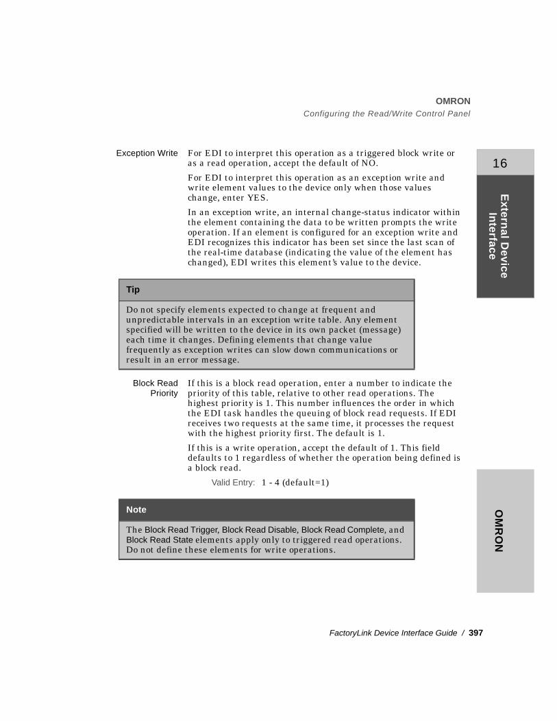
FactoryLink Device Interface Guide / 397
OM
RO
N
16
Extern
al Device
Interface
OMRONConfiguring the Read/Write Control Panel
Exception Write For EDI to interpret this operation as a triggered block write or as a read operation, accept the default of NO.
For EDI to interpret this operation as an exception write and write element values to the device only when those values change, enter YES.
In an exception write, an internal change-status indicator within the element containing the data to be written prompts the write operation. If an element is configured for an exception write and EDI recognizes this indicator has been set since the last scan of the real-time database (indicating the value of the element has changed), EDI writes this element’s value to the device.
Block ReadPriority
If this is a block read operation, enter a number to indicate the priority of this table, relative to other read operations. The highest priority is 1. This number influences the order in which the EDI task handles the queuing of block read requests. If EDI receives two requests at the same time, it processes the request with the highest priority first. The default is 1.
If this is a write operation, accept the default of 1. This field defaults to 1 regardless of whether the operation being defined is a block read.
Valid Entry: 1 - 4 (default=1)
Tip
Do not specify elements expected to change at frequent and unpredictable intervals in an exception write table. Any element specified will be written to the device in its own packet (message) each time it changes. Defining elements that change value frequently as exception writes can slow down communications or result in an error message.
Note
The Block Read Trigger, Block Read Disable, Block Read Complete, and Block Read State elements apply only to triggered read operations. Do not define these elements for write operations.

398 / FactoryLink Device Interface Guide
••••
OMRONConfiguring the Read/Write Control Panel
Block ReadTrigger
If this is a write operation, ignore this field.
If this is a triggered read operation, this field is required. Enter a tag name for a digital element to initiate a block read of the addresses specified in the Read/Write Information panel. When this element’s value is forced to 1 (ON), the addresses are read.
Valid Entry: standard element tag name Valid Data Type: digital
Block ReadDisable
If this is a write operation, ignore this field.
If this is a triggered read operation, this field is optional. If you need a digital element to disable a block read of the elements specified in this table, enter a tag name. When this tag’s value is forced to 1 (ON), the read operation is not executed, even when the block read trigger is set to 1.
To re-enable a block read table that has been disabled, set this element back to 0 (OFF).
Valid Entry: standard element tag nameValid Data Type: digital
Block ReadComplete
If this is a write operation, ignore this field.
If this is a triggered read operation, this field is optional. If you need a digital element to indicate when this operation is complete, enter a tag name. This element is forced to 1 (ON) at startup. After the elements defined in the Read/Write Information panel have been updated in the FactoryLink database, the complete element is forced to 1 again.
Do not use this element when more than one logical port is specified in a single table.
Valid Entry: standard element tag name Valid Data Type: digital
Tip
This element can be used to disable a block read operation that is either part of a cascaded loop or is self-triggered. The triggering cycle will cease upon disabling, however. To re-enable a cascaded loop or a self-triggered read table, the Block Read Trigger element must be toggled or forced to 1. Refer to Chapter 8, “Application Design Tips and Techniques,” for further details.

FactoryLink Device Interface Guide / 399
OM
RO
N
16
Extern
al Device
Interface
OMRONConfiguring the Read/Write Control Panel
Block Read State If this is a write operation, ignore this field.
If this is a triggered read operation, this field is optional. If you need a digital element to indicate the state of this operation (in progress or complete), enter a tag name. This element is forced to 1 (ON) at startup. While the table is being processed, the element is set to 0 (OFF). After the elements defined in the Read/Write Information panel have been updated in the FactoryLink database, the state element is forced back to 1.
Valid Entry: standard element tag name Valid Data Type: digital
Block WritePriority
If this is a block or exception write operation, enter a number to indicate the priority of this table, relative to other write operations. The highest priority is 1. This number influences the order in which the EDI task handles the queuing of write requests. If EDI receives two requests at the same time, it processes the request with the highest priority first. The default is 1.
If this is a read operation, accept the default of 1. This field defaults to 1 regardless of whether the operation being defined is a block or exception write.
Valid Entry: 1 - 4 (default=1)
Block Write Trigger If this is a read operation or an exception write operation you do not plan to periodically disable, ignore this field.
If this is a block write table or an exception write table you plan to periodically disable, this field is required. Enter a tag name for a digital element to initiate a block write of the element values specified in the Read/Write Information panel to the addresses defined to receive the values. When this element’s value is forced to 1 (ON), FactoryLink writes the values.
Valid Entry: standard element tag nameValid Data Type: digital
Note
The Block Write Trigger, Block Write Disable, Block Write Complete, and Block Write State elements apply only to write operations. Do not define these elements for read operations.

400 / FactoryLink Device Interface Guide
••••
OMRONConfiguring the Read/Write Control Panel
Block WriteDisable
If this is a read operation or an exception write operation you do not plan to periodically disable, ignore this field.
If this is a block write table or an exception write table you plan to periodically disable, this field is optional. Enter a tag name for a digital element to disable a block write to the addresses specified in this table. When this tag’s value is forced to 1 (ON), the write operation is not executed, even when the block write trigger is set to 1.
To re-enable a block write table that has been disabled, set this element back to 0 (OFF).
Valid Entry: standard element tag name Valid Data Type: digital
Block WriteComplete
If this is a read or exception write operation, ignore this field.
If this is a block write table, this field is optional. If you need a digital element to indicate when this operation is complete, enter a tag name. This element is forced to 1 (ON) at startup. After the data defined in this table’s Read/Write Information panel has been written to the device, the complete element is forced to 1 again.
Do not use this element when more than one logical port is specified in a single table.
Valid Entry: standard element tag name Valid Data Type: digital
Block Write State If this is a read or exception write operation, ignore this field.
If this is a block write operation, this field is optional. If you need a digital element to indicate the state of this operation (in progress or complete), enter a tag name. This element is forced to 1 (ON) at startup. While the table is being processed, the element
Tip
This element can be used to disable a block write operation that is either part of a cascaded loop or is self-triggered. The triggering cycle will cease upon disabling, however. To re-enable a cascaded loop or a self-triggered write table, the Block Write Trigger element must be toggled or forced to 1. Refer to Chapter 8, “Application Design Tips and Techniques,” for further details.

FactoryLink Device Interface Guide / 401
OM
RO
N
16
Extern
al Device
Interface
OMRONConfiguring the Read/Write Control Panel
is set to 0 (OFF). After the data defined in this table’s Read/Write Information panel has been written to the device, the state element is forced back to 1.
Do not use this element when more than one logical port is specified in a single table.
Valid Entry: standard element tag name Valid Data Type: digital
When the panel is complete, click Enter to validate the information. Define the data type (digital) for any tag names displayed in the Tag Definition dialog.
Table 16-3 provides sample entries for the OMRON Read/Write Control panel:
Table 16-3 Sample OMRON Read/Write Control Panel Entries
Field Entry Description
Table Name READ Specifies the table name.
Exception Write NO The table will not perform exception writes.
Block Read Priority 1 The block read priority for the table will be 1.
Block Read Trigger OMRN_READ_TRIGGER
When the value of OMRN_READ_TRIGGER is 1 or (on), a block read of values specified by the Read/Write Information panel associated with table 1 occurs.
Block Read Disable OMRN_READ_DISABLE
This element is defined to disable the block read operations.
Block Read Complete OMRN_READ_COMPLETE
The value of OMRN_READ_COMPLETE is set to 1 when the read is complete.
Block Read State OMRN_READ_STATE
The value for OMRN_READ_STATE is set to 1 if a read operation of table 1 is in progress, and the value is 0 if it is inactive.

402 / FactoryLink Device Interface Guide
••••
OMRONConfiguring the Read/Write Control Panel
Block Write Priority 1 The write priority for this table is set to 1 by default.
Block Write Trigger Since this is a read table, the elements specific to write requests are not defined.
Block Write Complete
Block Write Disable
Block Write State
Table 16-3 Sample OMRON Read/Write Control Panel Entries
Field Entry Description

FactoryLink Device Interface Guide / 403
OM
RO
N
16
Extern
al Device
Interface
OMRONConfiguring the Read/Write Information Panel
CONFIGURING THE READ/WRITE INFORMATION PANEL
From the Read/Write Control panel, select the row for the table you are configuring and click Next to bring the Read/Write Information panel to the foreground.
For a Read Table—Add a panel entry for each FactoryLink database element in which data read from the device will be stored when the operation executes.
For a Write Table—Add a panel entry for each element to be written when the operation executes.
Tag Name For a read table, specify a tag name for an element in which FactoryLink will store the data read from the device.
For a write table, specify a tag name for an element containing a value to be written to the device.
Valid Entry: standard element tag nameValid Data Type: digital, analog, float
Tip
Alternatively, the elements you define in the Read/Write Information panel can be configured in the Tag Definition dialog in the Application Editor. Refer to the Application Editor User Guide for details.

404 / FactoryLink Device Interface Guide
••••
OMRONConfiguring the Read/Write Information Panel
Logical Station Enter the number representing the device from which the data is to be read or to which the element’s value will be written. This number was originally defined in the Logical Station Information panel for the logical port through which communications with this device occurs.
Valid Entry: previously defined logical station number
Data Area Enter the data area of the OMRON controller to be read/written.
Refer to “OMRON Data Types and PLC Data Areas” on page 408 for more information about these data areas.
ST PLC operating status; channel number is ignored. Use element type A and data type BIN1.
ER PLC errors; channel number must be 0 or 1 for error word 1 or 2, respectively. Use data type BIN1.
IR I/O and internal relay area.
HR Holding relay area.
AR Auxiliary relay area.
LR Link relay area.
TC Timer/counter area. Use element type D and data type TCTR.
DM Data memory area.
PV Present value area. Use element type A or F and data type BCD1, BCD2, TIM, or TIMH.
Channel Enter the channel number within the data area of the value to be read or written.
Valid Entry: 0 - 9999
Bit Offset This field is required for digital data type. If the element (entry in the Tag Name column) associated with this entry is digital, enter the bit offset within the word that contains the value to be read or to which the element value is to be written. Bit 1 is the most significant bit (MSB) and bit 16 is the least significant bit.
Leave this field blank for all other FactoryLink data types.
Valid Entry: 0 (least significant bit), 15 (most significant bit)

FactoryLink Device Interface Guide / 405
OM
RO
N
16
Extern
al Device
Interface
OMRONConfiguring the Read/Write Information Panel
Data Type Specify the type of data being read from or written to the device for each element defined in the Tag Name field. Refer to “OMRON Data Types and PLC Data Areas” on page 408 for valid data types.
BIN1 16-bit binary value (-32768 to 32767). Use element type D or A.
BIN2 Two consecutive 16-bit binary values or 32-bit binary value (0 to 4294967295). Use element type F.
BCD1 16-bit BCD value (0 to 9999). Use element type A.
BCD2 Two consecutive 16-bit BCD values or 32-bit BCD value (0 to 9999999). Use element type F.
TIM 16-bit timer BCD value with units of 0.1 second (0.0 to 999.9). Use element type F.
TIMH 16-bit high-speed timer BCD value with units of 0.01 second (0.00 to 99.99). Use element type F.
TCTR One-bit timer/counter value (0 or 1). Use element type D and data area TC.
When the panel is complete, click Enter to validate the information. Define the data type (digital, analog, or floating-point) for any tag names displayed in the Tag Definition dialog.

OMRONConfiguring the Read/Write Information Panel
406 / FactoryLink Device Interface Guide
••••
Table 16-4 provides sample entries for the OMRON1 Read/Write Information panel:
Table 16-4 Sample OMRON Read/Write Information Panel Entries
Field Entry Description
Table Name READ Specifies the Read/Write table name.
Tag Name OMRNRDR1 The value read from the device is stored in OMRNRDR1.
Logical Station 0 Specifies the path to send the request.
Data Area IR Data area of the controller to be read/written.
Channel 10 Channel number in the external device.
Bit Offset 1 Specific location of information to read.
Data Type BIN1 Data type read from or written to this controller.

FactoryLink Device Interface Guide / 407
OM
RO
N
16
Extern
al Device
Interface
OMRONTechnical Notes: Monitor Mode
TECHNICAL NOTES: MONITOR MODE
The OMRON PLC operates in the RUN, MONITOR, or PROGRAM modes. For the FactoryLink OMRON protocol module to write to an external device, ensure that the OMRON PLC is in the MONITOR mode by setting the switch on the OMRON Programming Console to MONITOR. In this mode, the OMRON PLC monitors bit or channel data from the data areas or specific program addresses and reads it to the FactoryLink real-time database.
Some OMRON factory configurations operate normally in MONITOR mode. In this case, writes to the PLC will occur normally and no other actions are needed.
Other OMRON factory configurations may require that the PLC operate in RUN or PROGRAM mode. If this is necessary, override the setting on the Programming Console and place the PLC in MONITOR mode using the following procedure:
In the OMRON Read/Write Information panel, configure an analog element.
Enter ST in the Data Area field (for the OMRON PLC operating status) and enter BIN1 in the Data Type field.
To change the operating mode of the PLC to the MONITOR mode, force write an 02 (which represents MONITOR mode in the ST area) to the FactoryLink analog element.
For further information about the OMRON Status Write and changing the operating mode, refer to the OMRON Host Link Unit Operation Manual.
To avoid manually performing this procedure each time you start FactoryLink, configure Math and Logic to perform this operation automatically at startup. For further information about configuring the Math and Logic task, refer to “Configuring Math & Logic” in the FactoryLink ECS Configuration Guide.

OMRONOMRON Data Types and PLC Data Areas
408 / FactoryLink Device Interface Guide
••••
OMRON DATA TYPES AND PLC DATA AREAS
The following table shows the FactoryLink data types and the OMRON data types that are to be used for each OMRON PLC data area:
Table 16-5 Data Types and PLC Data Areas
FactoryLink Data Type OMRON Data Type OMRON PLC Data Area
D BIN1 ER
BIN1 IR, HR, AR
TCTR TC
A BIN1 ST
BIN1 ER
BIN1 IR, HR, AR
BCD1 LR and DM
BCD1 PV
F BIN2 IR, HR, AR
BCD2 LR and DM
TIM LR and DM
TIMH LR and DM
BCD2 PV
TIM PV

FactoryLink Device Interface Guide / 409
OM
RO
N
16
Extern
al Device
Interface
OMRONRun-Time Application Messages
RUN-TIME APPLICATION MESSAGES
During EDI run time, FactoryLink generates and displays messages for the Omron protocol module on the Run-Time Manager screen and, if so configured, writes them to message or analog tags. For information about configuring a message tag, see “Configuring the Logical Station Control Panel” on page 390 of this guide. For information about configuring an analog tag, see “Configuring the Logical Station Information Panel” on page 393 of this guide.
For information about the messages displayed for the EDI task and the format in which protocol module messages are generated, see Chapter 10, “Messages and Codes,” of this guide.
The ER: string in a message can contain either a single-character or a double-character error code. In following descriptions, n represents the significant characters of the error.• Single-Character Code Format
ER:000n is a single-character format in which one character represents a single error condition. In some cases, two individual codes appear within a string to indicate multiple error conditions.
• Double-Character Code Format
ER:00nn is a double-character format in which two characters represent a single error condition. Decode the ER:00nn string by interpreting nn’s most significant digit (MSD), the leftmost integer, and least significant digit (LSD), the rightmost integer.

OMRONRun-Time Application Messages
410 / FactoryLink Device Interface Guide
••••
OMRON Error Codes
The following error code values occur in the LSD.
Example:
If: ER:0043
Then: MSD = 4
LSD = 3
Case 0: ER:000e OMRON Response Errors
1
Cause: Not executable in RUN mode.
Action: Command request cannot be performed with the device in RUN mode.
2
Cause: Not executable in MONITOR mode.
Action: Command request cannot be performed with the device in MONITOR mode.
3
Cause: Not executable with PROM mounted.
Action: Command request cannot be performed with the device with PROM mounted.
4
Cause: Address over (data overflow).
B
Cause: Not executable in PROGRAM mode.
Action: Command request cannot be performed with the device in PROGRAM mode.

FactoryLink Device Interface Guide / 411
OM
RO
N
16
Extern
al Device
Interface
OMRONRun-Time Application Messages
C
Cause: Not executable with PROM mounted.
Action: Command request cannot be performed with the device with PROM mounted.
D
Cause: Not executable in LOCAL mode.
Action: Command request cannot be performed with the device in LOCAL mode.
Case 1: ER:001e OMRON Response Errors
0
Cause: Parity error.
Action: Verify the parity setup matches the device.
1
Cause: Framing error.
Action: Verify the number of data and stop bits set up matches the device.
2
Cause: Overrun.
Action: Verify the number of data and stop bits setup matches the device.
3
Cause: FCS error.
Action: Verify the parity and the number of data and stop bits setup matches the device.

OMRONRun-Time Application Messages
412 / FactoryLink Device Interface Guide
••••
4
Cause: Format error (parameter length error).
Action: Verify the Read/Write configuration panel entries are valid for device parameter. Contact Customer Support if the problem persists.
5
Cause: Entry number data error (parameter error, data code error, data length error).
Action: Verify the Read/Write configuration panel entries are valid for device parameter. Contact Customer Support if the problem persists.
6
Cause: Instruction not found.
Action: Verify the Read/Write configuration panel entries are valid for device parameter. Contact Customer Support if the problem persists.
8
Cause: Frame length error.
Action: Verify the Read/Write configuration panel entries are valid for device parameter. Contact Customer Support if the problem persists.
9
Cause: Command not executable due to inexecutable error clear, non-registration of I/O table, etc.
Action: Contact OMRON for more information.

FactoryLink Device Interface Guide / 413
OM
RO
N
16
Extern
al Device
Interface
OMRONRun-Time Application Messages
Case 2: ER:002e OMRON Response Errors
0
Cause: I/O table generation impossible due to unrecognized Remote I/O Unit, channel over, or duplication of Optical Transmitting I/O Unit.
Action: Contact OMRON for more information.
Case 3: ER:003e Read/write Request Aborted
1
Cause: Transmit error.
Action: Verify the cable has been constructed properly and that it is connected to the logical port and device.
Case 4: ER:004e Read/Write Request Reception Error
2
Cause: Timeout error.
Action: Verify the cable has been connected to the logical port and device. Also, check that the timeout period has been defined for the recommended time.
3
Cause: Received invalid response character.
Action: Verify the parity and the number of data and stop bits are configured properly for the device. Also, verify the cable ground wire is connected properly.
4
Cause: Reception buffer overflow. Response too large for reception buffer.
Action: Contact Customer Support immediately.

OMRONRun-Time Application Messages
414 / FactoryLink Device Interface Guide
••••
5
Cause: Received invalid start of data response character.
Action: Verify the parity and the number of data and stop bits are configured properly for the device.
6
Cause: Received NAK response for command request.
Action: Verify the Read/Write configuration panel entries are valid for device parameter. Also, verify the parity and the number of data and stop bits are configured properly for the device and that the cable ground wire is connected properly.
Case 5: ER:005e OMRON Response Packet Errors
0
Cause: Queuing read request error.
Action: Verify the IBM RIC/ARTIC board and the OMRON protocol module have sufficient data storage defined. Contact Customer Support if the problem persists.
1
Cause: Queuing write request error.
Action: Verify the IBM RIC/ARTIC board and the OMRON protocol module have sufficient data storage defined. Contact Customer Support if the problem persists.
2
Cause: Read or write request too large for the transmit buffer.
Action: Contact Customer Support immediately.
3
Cause: OMRON read/write response produced an unknown error.
Action: Contact Customer Support immediately.

FactoryLink Device Interface Guide / 415
OM
RO
N
16
Extern
al Device
Interface
OMRONRun-Time Application Messages
Case A: ER:00Ae OMRON Response Errors
0
Cause: Aborted due to parity error in transmit data.
Action: Verify the parity setup matches the device.
1
Cause: Aborted due to framing error in transmit data.
Action: Verify the number of data and stop bits setup matches the device.
2
Cause: Aborted due to overrun in transmit data.
Action: Verify the number of data and stop bits set up matches the device.
4
Cause: Aborted due to format error in transmit data.
Action: Verify the Read/Write configuration panel entries are valid for device parameter. Contact Customer Support if the problem persists.
5
Cause: Aborted due to entry number data error in transmit data.
Action: Verify the Read/Write configuration panel entries are valid for device parameter. Contact Customer Support if the problem persists.
8
Cause: Aborted due to frame length error in transmit data.
Action: Verify the Read/Write configuration panel entries are valid for device parameter. Contact Customer Support if the problem persists.

OMRONRun-Time Application Messages
416 / FactoryLink Device Interface Guide
••••
Case B: ER:00Be OMRON Response Errors
0
Cause: Not executable because program area is not 16K bytes.

FactoryLink Device Interface Guide / 417
17
Extern
al Device
Interface
• • • •
Siem
ens C
P525
Chapter 17
Siemens CP525
This chapter contains information to set up and configure bidirectional communications between the FactoryLink real-time database and the Siemens CP525 using RK512 with either 3964 or 3964R protocol.
When you choose Siemens CP525 from the Configuration Manager Main Menu, the Siemens CP525 configuration panels are displayed.
Note
Before completing the protocol-specific Siemens CP525 configuration panels, you must complete the External Device Definition panel. See “Identifying Protocol Types and Defining Logical Ports” on page 70 for details.

418 / FactoryLink Device Interface Guide
••••
SIEMENS CP525Configuring the Logical Station Control Panel
CONFIGURING THE LOGICAL STATION CONTROL PANEL
To bring the Logical Station Control panel to the foreground, click its title bar in the display of all configuration panels.
Complete a row for each logical port specified in the External Device Definition panel you want to define as a communication path for read and write operations.
Logical Port Enter a number, defined in the External Device Definition panel Logical Port column, to represent a particular communication path to a device.
Valid Entry: previously defined logical port number
Baud Rate Enter the speed at which the protocol module communicates with the devices linked to FactoryLink via this logical port. This entry must match the baud rate configuration of the devices. Refer to the device manufacturer ’s documentation for details.
Valid Entry: 110 - 115200 (default=9600)
Parity Enter the parity error correction during transmission via this logical port. This entry must match the configuration of the devices communicating via this port. Refer to the device manufacturer’s documentation for details.
Valid Entry: none, even, odd (default=even)

FactoryLink Device Interface Guide / 419
17
Extern
al Device
Interface
Siem
ens C
P525
SIEMENS CP525Configuring the Logical Station Control Panel
Data Bits Enter the number of data bits used during transmission via this logical port. This entry must match the configuration of the devices communicating via this port. Refer to the device manufacturer’s documentation for details.
Valid Entry: 7, 8 (default=8)
Stop Bits Enter the number of bits sent after a character to create a pause before the start of the next character. This entry must match the configuration of the devices communicating via this port. Refer to the device manufacturer ’s documentation for details.
Valid Entry: 1, 2 (default=1)
ResponseTimeout 0.1 Sec
Enter the length of time, in tenths of a second, the protocol module will wait to receive a response to a read or write command before timing out. You must enter a value greater than 0 for the protocol module to timeout.
Valid Entry: standard Siemens timeouts, based on the baud rate (default=0)
LRC ErrorDetection
Enter the type of error detection protocol.
None Siemens Procedure 3964
BCC (Default) Siemens Procedure 3964R
Retry Request Enter the maximum number of times the protocol module will retry a read or write command to a device communicating through this logical port if the command response is invalid or is not received.
Valid Entry: 0 - 65535 (default=3)
Master/Slave Indicate whether the FactoryLink station is the Master or the Slave of the communications channel.
M (Default) Master
S Slave
Status Msg Tag (Optional) Enter a tag name for a message element to which a text string will be written to indicate a communications error associated with this logical port.
Valid Entry: standard element tag nameValid Data Type: message

420 / FactoryLink Device Interface Guide
••••
SIEMENS CP525Configuring the Logical Station Control Panel
When the panel is complete, click Enter to validate the information. Define the data type (message) for any tag names displayed in the Tag Definition dialog.
Table 17-1 provides sample entries for the Siemens 525 Logical Station Control panel:
Table 17-1 Sample Siemens 525 Logical Station Control Panel Entries
Field Entry Description
Logical Port 0 Specifies the logical communication path configured by this table.
Baud Rate 9600 Specifies the communication rate.
Parity EVEN Adds a parity bit to the sum of the transmitted bits to make it even.
Data Bits 8 Specifies 8 data bits in the transmission.
Stop Bits 1 Specifies 1 stop bit in the transmission.
Response Timeout (0.1 Sec)
100 The response timeout is 10 seconds.
LRC Error Detection BCC Specifies the error checking method.
Retry Request 3 Attempt the request three times before generating a timeout.
Master/Slave M Master (default).
Status Msg Tag SIEM_LPORT0_MSG
Message tag containing Siemens error messages.

FactoryLink Device Interface Guide / 421
17
Extern
al Device
Interface
Siem
ens C
P525
SIEMENS CP525Configuring the Logical Station Information Panel
CONFIGURING THE LOGICAL STATION INFORMATION PANEL
From the Logical Station Control panel, select the row for the logical port you are configuring and click Next to bring the Logical Station Information panel to the foreground.
Complete a row for each device to communicate through this logical port.
Error /Status TagName
(Optional) Enter a tag name for an analog element in which to store communications error codes associated with this device (logical station).
You can animate output-text objects to display the codes stored in an Error/Status Tag Name element on a graphics screen. Refer to the Application Editor User Guide for more information.
Valid Entry: standard element tag nameValid Data Type: analog
Logical Station Enter a number to identify the logical station to which the information in this row pertains. A logical station represents the combination of a logical port with a physical station. Assign a unique number to each device communicating through this logical port.

422 / FactoryLink Device Interface Guide
••••
SIEMENS CP525Configuring the Logical Station Information Panel
You will later enter this logical station number in a read or write table to represent the device defined in this row. In a read or write table, this number will identify the device to or from which data is to be sent or received.
Valid Entry: 0 - 999
Max PacketLength
Define the maximum number of bytes the device defined in this row can transmit in one message. Most devices can transmit 256 bytes, or 128 registers of data. The protocol being used (point-to-point or IEEE 802.3) does not affect the maximum packet size.
Valid Entry: 32, 64
Comment (Optional) Enter reference information about this logical station.
Valid Entry: alphanumeric string of up to 21 characters
When the panel is complete, click Enter to validate the information. Define the data type (analog) for any tag names displayed in the Tag Definition dialog.
Table 17-2 provides sample entries for the Siemens 525 Logical Station Information panel:
Table 17-2 Sample Siemens 525 Logical Station Information Panel Entries
Field Entry Description
Error/Status Tag Name SIEM_STATION0_STATUS
Contains information about communication errors.
Logical Station 0 Specifies the logical communication path.
Max Packet Length 64 Maximum packet length is 64.

FactoryLink Device Interface Guide / 423
17
Extern
al Device
Interface
Siem
ens C
P525
SIEMENS CP525Configuring the Read/Write Control Panel
CONFIGURING THE READ/WRITE CONTROL PANEL
To bring the Read/Write Control panel to the foreground, click its title bar in the display of all configuration panels or click Next from the Logical Station Information panel.
Complete a row for each read or write table.
Table Name Give this read or write request a name. Define one request (table) per line and do not include spaces in the name. You can define as many tables in this panel as available memory allows. Try to make the table name reflective of the operation it represents.
If this is a triggered read or a block write table, when the trigger element (Block Read Trigger for a read operation or Block Write Trigger for a write operation) is forced to 1 (ON), the element prompts FactoryLink to process this table and any other table in which the same trigger is defined.
Valid Entry: alphanumeric string of up to 16 characters
Tip
Refer to Chapter 8, “Application Design Tips and Techniques,” for information about triggering schemes using elements defined in this panel.

424 / FactoryLink Device Interface Guide
••••
SIEMENS CP525Configuring the Read/Write Control Panel
Unsolicited Read For EDI to interpret this operation as a triggered block read or as a write operation, accept the default of NO.
If this is an unsolicited read operation, enter YES or FORCE. EDI will interpret this operation as an unsolicited read and emulate the device’s addressing structure based on entries you make in the Read/Write Information panel. The incoming data will be stored in the real-time database as specified in this field.
If you enter YES, the incoming data will be stored in the element represented by the tag name specified in the Read/Write Information panel. If the current value of the element is equal to the new value, the change-status indicator is unaffected. If a different value is being stored the element, however, it will overwrite the current value and the element’s change-status indicator will be set to 1 (ON).
If you enter FORCE, the data is stored in the specified element and the change-status indicator is automatically set to 1, regardless of whether the current value matches the new value.
Valid Entry: yes, no, force (default=no)
Exception Write For EDI to interpret this operation as a triggered block write or as a read operation, accept the default of NO.
For EDI to interpret this operation as an exception write and write element values to the device only when those values change, enter YES. Do not specify elements expected to change at frequent and unpredictable intervals in an exception write table. Any element specified will be written to the device in its own packet (message) each time it changes. Defining elements that change value frequently as exception writes can slow down communications or result in an error message.
In an exception write, an internal change-status indicator within the element containing the data to be written prompts the write operation. If an element is configured for an exception write and EDI recognizes this indicator has been set since the last scan of the real-time database (indicating the value of the element has changed), EDI writes this element’s value to the device.
Valid Entry: yes, no (default=no)

FactoryLink Device Interface Guide / 425
17
Extern
al Device
Interface
Siem
ens C
P525
SIEMENS CP525Configuring the Read/Write Control Panel
Block ReadPriority
If this is a block read operation, enter a number to indicate the priority of this table, relative to other read operations. The highest priority is 1. This number influences the order in which the EDI task handles the queuing of block read requests. If EDI receives two requests at the same time, it processes the request with the highest priority first. The default is 1.
If this is an unsolicited read or a write operation, accept the default of 1. This field defaults to 1 regardless of whether the operation being defined is a block read.
Valid Entry: 1 - 4 (default=1)
Block ReadTrigger
If this is an unsolicited read or a write operation, ignore this field.
If this is a triggered read operation, this field is required. Enter a tag name for a digital element to initiate a block read of the addresses specified in the Read/Write Information panel. When this element’s value is forced to 1 (ON), the addresses are read.
Valid Entry: standard element tag nameValid Data Type: digital
Note
The Block Read Trigger, Block Read Disable, Block Read Complete, and Block Read State elements apply only to triggered read operations. Do not define these elements for unsolicited read operations or for write operations.
Tip
The Block Read Disable element can be used to disable a block read operation that is either part of a cascaded loop or is self-triggered. The triggering cycle will cease upon disabling, however. To re-enable a cascaded loop or a self-triggered read table, the Block Read Trigger element must be toggled or forced to 1. Refer to Chapter 8, “Application Design Tips and Techniques,” for details.

426 / FactoryLink Device Interface Guide
••••
SIEMENS CP525Configuring the Read/Write Control Panel
Block ReadDisable
If this is an unsolicited read or a write operation, ignore this field.
If this is a triggered read operation, this field is optional. If you need a digital element to disable a block read of the elements specified in this table, enter a tag name. When this tag’s value is forced to 1 (ON), the read operation is not executed, even when the block read trigger is set to 1.
To re-enable a block read table that has been disabled, set this element back to 0 (OFF).
Valid Entry: standard element tag nameValid Data Type: digital
Block ReadComplete
If this is an unsolicited read or a write operation, ignore this field.
If this is a triggered read operation, this field is optional. If you need a digital element to indicate when this operation is complete, enter a tag name. This element is forced to 1 (ON) at startup. After the elements defined in the Read/Write Information panel have been updated in the FactoryLink database, the complete element is forced to 1 again.
Do not use this element when more than one logical port is specified in a single table.
Valid Entry: standard element tag nameValid Data Type: digital
Block Read State If this is an unsolicited read or a write operation, ignore this field.
If this is a triggered read operation, this field is optional. If you need a digital element to indicate the state of this operation (in progress or complete), enter a tag name. This element is forced to 1 (ON) at startup. While the table is being processed, the element is set to 0 (OFF). After the elements defined in the Read/Write Information panel have been updated in the FactoryLink database, the state element is forced back to 1.
Valid Entry: standard element tag nameValid Data Type: digital
Block WritePriority
If this is a block or exception write operation, enter a number to indicate the priority of this table, relative to other write operations. The highest priority is 1. This number influences the order in which the EDI task handles the queuing of write requests. If EDI receives two requests at the same time, it processes the request with the highest priority first. The default is 1.

FactoryLink Device Interface Guide / 427
17
Extern
al Device
Interface
Siem
ens C
P525
SIEMENS CP525Configuring the Read/Write Control Panel
If this is a read operation, accept the default of 1. This field defaults to 1 regardless of whether the operation being defined is a block or exception write.
Valid Entry: 1 - 4 (default=1)
Block Write Trigger If this is a read operation or an exception write operation you do not plan to periodically disable, ignore this field.
If this is a block write table or an exception write table you plan to periodically disable, this field is required. Enter a tag name for a digital element to initiate a block write of the element values specified in the Read/Write Information panel to the addresses defined to receive the values. When this element’s value is forced to 1 (ON), FactoryLink writes the values.
Valid Entry: standard element tag nameValid Data Type: digital
Block WriteDisable
If this is a read operation or an exception write operation you do not plan to periodically disable, ignore this field.
If this is a block write table or an exception write table you plan to periodically disable, this field is optional. Enter a tag name for a digital element to disable a block write to the addresses specified in this table. When this tag’s value is forced to 1 (ON), the write operation is not executed, even when the block write trigger is set to 1.
Note
The Block Write Trigger, Block Write Disable, Block Write Complete, and Block Write State elements apply only to write operations. Do not define these elements for read operations.
Tip
The Block Write Disable element can be used to disable a block write operation that is either part of a cascaded loop or is self-triggered. The triggering cycle will cease upon disabling, however. To re-enable a cascaded loop or a self-triggered write table, the Block Write Trigger element must be toggled or forced to 1. Refer to Chapter 8, “Application Design Tips and Techniques,” for further details.

428 / FactoryLink Device Interface Guide
••••
SIEMENS CP525Configuring the Read/Write Control Panel
To re-enable a block write table that has been disabled, set this element back to 0 (OFF).
Valid Entry: standard element tag nameValid Data Type: digital
Block WriteComplete
If this is a read or exception write operation, ignore this field.
If this is a block write table, this field is optional. If you need a digital element to indicate when this operation is complete, enter a tag name. This element is forced to 1 (ON) at startup. After the data defined in this table’s Read/Write Information panel has been written to the device, the complete element is forced to 1 again.
Do not use this element when more than one logical port is specified in a single table.
Valid Entry: standard element tag nameValid Data Type: digital
Block Write State If this is a read or exception write operation, ignore this field.
If this is a block write operation, this field is optional. If you need a digital element to indicate the state of this operation (in progress or complete), enter a tag name. This element is forced to 1 (ON) at startup. While the table is being processed, the element is set to 0 (OFF). After the data defined in this table’s Read/Write Information panel has been written to the device, the state element is forced back to 1.
Do not use this element when more than one logical port is specified in a single table.
Valid Entry: standard element tag nameValid Data Type: digital
When the panel is complete, click Enter to validate the information. Define the data type (digital) for any tag names displayed in the Tag Definition dialog.

FactoryLink Device Interface Guide / 429
17
Extern
al Device
Interface
Siem
ens C
P525
SIEMENS CP525Configuring the Read/Write Control Panel
Table 17-3 provides sample entries for the Siemens 525 Read/Write Control panel:
Table 17-3 Sample Siemens 525 Read/Write Control Panel Entries
Field Entry Description
Table Name READ Specifies the table name.
Unsolicited Read NO Table will not perform unsolicited reads.
Exception Write NO Table will not perform exception writes.
Block Read Priority 1 Priority for tables set to 1.
Block Read Trigger SIEM_READ_TRIGGER
When the value of SIEM_READ_TRIGGER is 1 or (on), a block read of values specified by the Read/Write Information panel associated with SIEMBRD occurs.
Block Write Priority 1 The write priority for this table is set to 1 by default.
Block Write Trigger Since this is a read table, the elements specific to write requests are not defined.
Block Write Complete
Block Write Disable
Block Write State

430 / FactoryLink Device Interface Guide
••••
SIEMENS CP525Configuring the Read/Write Information Panel
CONFIGURING THE READ/WRITE INFORMATION PANEL
From the Read/Write Control panel, select the row for the table you are configuring and click Next to bring the Read/Write Information panel to the foreground.
For a Read Table—Add a panel entry for each FactoryLink database element in which data read from the device will be stored when the operation executes.
For a Write Table—Add a panel entry for each element to be written when the operation executes.
Tip
Alternatively, the elements you define in the Read/Write Information panel can be configured in the Tag Definition dialog in the Application Editor. Refer to the Application Editor User Guide for details.

FactoryLink Device Interface Guide / 431
17
Extern
al Device
Interface
Siem
ens C
P525
SIEMENS CP525Configuring the Read/Write Information Panel
Tag Name For a read table, specify a tag name for an element in which FactoryLink will store the data read from the device.
For a write table, specify a tag name for an element containing a value to be written to the device.
Valid Entry: standard element tag nameValid Data Type: digital, analog, longana, float, message
Logical Station Enter the number representing the device from which the data is to be read or to which the element’s value will be written. This number was originally defined in the Logical Station Information panel for the logical port through which communications with this device occurs.
Valid Entry: previously defined logical station number
PLC Region Enter the data area of the PLC to be read/written.
For read operations:
CB Counters
DB Data block
DX Extended data block
FB Flag bytes
IB Input bytes
OB Output bytes
PB Peripheral blocks
TB Timers
For write operations:
DB Data block
DX Extended data block
Data Block Enter the data block number of the address to be read or written.
Valid Entry: 3 - 255
Word/ Byte Enter the address of word in word regions or address of byte in byte regions that is read or written.
0-255 CB, DB, DX, FB, PB, TB
0-127 IB, OB

432 / FactoryLink Device Interface Guide
••••
SIEMENS CP525Configuring the Read/Write Information Panel
Bit/Length (For digital elements) Bit in the word or byte that is read or written.
0 (LSB) - 15 (MSB): For word regions
0 (LSB) - 7 (MSB): For byte regions
(For message elements) Length in word or byte that is read or written.
Length in words: (For word regions) Limited to the packet size for the station: 64 = 64 words; 32 = 32 words
Length in bytes: (For byte regions) Limited to the packet size for the station: 64 = 128 bytes; 32 = 64 bytes
Data Type Specify the type of data being read from or written to the device for each element defined in the Tag Name field.
Valid Entry: Refer to “Siemens CP525 Data Types” on page 435.
CoordinationFlag CPU
Specify the number of the CPU that is to process the read or write operation or enter NONE for no CPU.
Valid Entry: NONE, 0 - 4 (default=NONE)
CoordinationFlag Byte
Specify the byte number of the coordination flag or enter NONE if no coordination flag is set.
Valid Entry: NONE, 0 - 254 (default=NONE)
CoordinationFlag Bit
Specify the bit number of the coordination flag or enter NONE if no coordination flag is set.
Valid Entry: NONE, 0 - 7 (default=NONE)
When the panel is complete, click Enter to validate the information. Define the data type (digital, analog, long analog, or floating-point) for any tag names displayed in the Tag Definition dialog.

FactoryLink Device Interface Guide / 433
17
Extern
al Device
Interface
Siem
ens C
P525
SIEMENS CP525Configuring the Read/Write Information Panel
Table 17-4 provides sample entries for the Siemens 525 Read/Write Information panel:
Table 17-4 Sample Siemens 525 Read/Write Information Panel Entries
Field Entry Description
Table Name READ Specifies the Read/Write table name.
Tag Name SIEMDIG1 The value read from the device will be stored in SIEMDIG1.
Logical Station 0 Specifies the path to send the request.
PLC Region DB Data block.
Data Block 10 Data block in the PLC to write the value of SIEMDIG1.
Word/Byte 6 Word/byte in the PLC to write the value of SIEMDIG1.
Bit/Length 3 Bit/length of the value written.
Data Type DW Defaults to Siemens data type BIN.
Coordination Flag CPU NONE
Coordination Flag Byte NONE
Coordination Flag Bit NONE

434 / FactoryLink Device Interface Guide
••••
SIEMENS CP525Siemens CP525 Switches
SIEMENS CP525 SWITCHES
For information about setting Siemens CP525 switches, refer to Section 3.4 of Siemens COM525 for CP524 and CP525 (S5-DOS), Volume 1, order number 6ES5998-1DB21, release 05.

FactoryLink Device Interface Guide / 435
17
Extern
al Device
Interface
Siem
ens C
P525
SIEMENS CP525Siemens CP525 Data Types
SIEMENS CP525 DATA TYPES
When you configure the Data Type field of the Siemens CP525 Read/Write Information panel, each FactoryLink data type has a default Siemens PLC data type. By using the PLC data type BIN, you may specify the default entry in configuration table. (For compatibility with previous versions, the Data Type DW defaults to BIN.) The following table shows the default conversions for each of the FactoryLink data types.
Each FactoryLink data type also has a range of valid Siemens PLC data types. You may choose to specify a Siemens PLC data type. The following table shows the FactoryLink data types, and the corresponding Siemens PLC data types.
Table 17-5 Default Conversions for FactoryLink Data Types
FactoryLink Data Types Siemens PLC Data Types
Digital DIG
Analog INT2
Longana INT4
Float FLT
Message LOHI
Table 17-6 Digital Conversion
PLC Type Conversion
DIG Single bit of a word or byte is read or written
Table 17-7 Analog Conversion
PLC Type Conversion
INT2 Converts the FactoryLink value to or from a 2-byte, signed integer

SIEMENS CP525Siemens CP525 Data Types
436 / FactoryLink Device Interface Guide
••••
INT4 Converts the FactoryLink value to or from a 4-byte, signed integer
BCD3 Converts the FactoryLink value to or from a 2-byte, unsigned, three-digit, binary-coded decimal
BCD7 Converts the FactoryLink value to or from a 4-byte, unsigned, seven-digit, binary-coded decimal
FLT Converts the FactoryLink value to or from a 4-byte, Siemens PLC floating-point
BYTE (Valid only in byte PLC regions) Converts the FactoryLink value to or from a single unsigned byte (0 - 255)
Table 17-8 Longana Conversion
PLC Type Conversion
INT2 Converts the FactoryLink value to or from a 2-byte, signed integer
INT4 Converts the FactoryLink value to or from a 4-byte signed integer
BCD3 Converts the FactoryLink value to or from a 2-byte, unsigned, three-digit, binary-coded decimal
BCD7 Converts the FactoryLink value to or from a four-digit, unsigned, seven-digit, binary-coded decimal
FLT Converts the FactoryLink value to or from a 4-byte Siemens PLC floating-point
BYTE (Valid only in byte PLC regions) Converts the FactoryLink value to or from a single unsigned byte (0 - 255)
Table 17-7 Analog Conversion (Continued)
PLC Type Conversion

FactoryLink Device Interface Guide / 437
17
Extern
al Device
Interface
Siem
ens C
P525
SIEMENS CP525Siemens CP525 Data Types
Table 17-9 Floating-Point Conversion
PLC Type Conversion
INT2 Converts the FactoryLink value to or from a 2-byte, signed integer
INT4 Converts the FactoryLink value to or from a 4-byte, signed integer
BCD3 Converts the FactoryLink value to or from a 2-byte, unsigned three-digit, binary-coded decimal
BCD7 Converts the FactoryLink value to or from a 4-byte, unsigned, seven-digit, binary-coded decimal
FLT Converts the FactoryLink value to or from a 4-byte, Siemens PLC Floating-point
BYTE (Valid only in byte PLC regions) Converts the FactoryLink value to or from a single, unsigned byte (0 - 255)
Table 17-10 Message Conversion
PLC Type Conversion
HILO Consecutive bytes in the FactoryLink message element are read or written to the PLC as a high-order (HI) byte followed by a low-order (LO) byte.
LOHI Consecutive bytes in the FactoryLink message element are read or written to the PLC as a low-order (LO) byte followed by a high-order (HI) byte.

SIEMENS CP525Run-Time Application Messages
438 / FactoryLink Device Interface Guide
••••
RUN-TIME APPLICATION MESSAGES
During EDI run time, FactoryLink generates and displays messages for the Siemens CP525 protocol module on the Run-Time Manager screen and, if so configured, writes them to message or analog tags. For information about configuring a message tag, see “Configuring the Logical Station Control Panel” on page 418. For information about configuring an analog tag, see “Configuring the Logical Station Information Panel” on page 421.
For information about the messages displayed for the EDI task and the format in which protocol module messages are generated, see Chapter 10, “Messages and Codes.”
The ER:xxxN string in a message contains a single-digit error code. N represents significant digits and x represents digits not significant to the error. ER:xxxN is a single-digit format in which one digit represents a single error condition. In some cases, two individual codes appear within a string to indicate multiple error conditions.
0001h
Cause: Internal error.
Action: Contact Customer Support.
0002h
Cause: Unable to successfully communicate with PLC.
Action: Check line parameters (baud rate, data bits, etc.), cable, CP525 programming.
0003h
Cause: Unable to receive response to read/write request.
Action: Check CP525 programming.
0004h
Cause: Internal error.
Action: Contact Customer Support.

FactoryLink Device Interface Guide / 439
17
Extern
al Device
Interface
Siem
ens C
P525
SIEMENS CP525Run-Time Application Messages
XX05h
Cause: Received error code XXh from Siemens PLC in response packet.
Action: Refer to Siemens CP525 documentation.
0006h
Cause: After retry count, received more or fewer bytes than requested in read request packet.
Action: Contact Customer Support.
0007h
Cause: Internal error.
Action: Contact Customer Support.

SIEMENS CP525Run-Time Application Messages
440 / FactoryLink Device Interface Guide
••••

Siem
ens H
1
FactoryLink Device Interface Guide / 441
18
Extern
al Device
Interface
• • • •Chapter 18
Siemens H1
This chapter contains information needed to set up and configure bidirectional communications between the FactoryLink real-time database and any Siemens Simatic S5 or S505 PLC using one of the following interfaces:• CP-535, CP-143 card• CP-1433, CP-1434 • Ethernet interface card over an Ethernet network
SIEMENS H1 COMMUNICATIONS
Communication in the Siemens H1 protocol module occurs between the Siemens Ethernet Interface and the Device Control Module (DCM) using logical entities called Transport Service Access Points (TSAPs).
TSAPs are communication points that link the Siemens Ethernet Interface and the DCM. TSAPs work in pairs. A DCM TSAP works with a Siemens Ethernet Interface TSAP, with one TSAP on each side of the communication link.
Types of Communication
On one side of the communication link, the DCM performs three types of communication. Each type of communication has an associated TSAP pair. The DCM performs the following types of communication:• Solicited Reads—Block reads of data from the Siemens PLC to the real-time
database. S5—The Read Active/Passive TSAP pair consists of a Fetch active TSAP in the DCM and a Fetch passive TSAP in the Siemens Ethernet Interface card.S505—The Read Active/Passive TSAP pair consists of a Read active TSAP in the DCM and a Read passive TSAP in the Siemens Ethernet Interface card.
• Solicited Writes—Block and exception writes of data from the real-time database to the Siemens PLC. S5—The Write Active/Passive TSAP pair consists of a Send active TSAP in the DCM and a Receive passive TSAP in the Siemens Ethernet Interface card.

442 / FactoryLink Device Interface Guide
••••
SIEMENS H1Siemens H1 Communications
S505—The Write Active/Passive TSAP pair consists of a Write active TSAP in the DCM and a Write passive TSAP in the Siemens Ethernet Interface card.
• Unsolicited Reads
S5—Siemens PLC-generated writes sending data from the Siemens PLC to the real-time database. The Write Active/Passive TSAP pair consists of a Receive passive in the DCM and a Send active in the Siemens Ethernet Interface card.S505—Siemens PLC-generated writes sending data from the Siemens PLC to the real-time database. The Write Active/Passive TSAP pair consists of a Write passive in the DCM and a Write active in the Siemens Ethernet Interface card.
Table 18-1 describes the relationships between the three types of communication performed by the DCM and the TSAP pairs.
where:
Active Describes the Siemens Interface co-processor jobs and denotes the initiator or “master” of the link.
Passive Describes the Siemens Interface co-processor jobs and denotes the receiver or “slave” of the link.
Table 18-1 Communications and the TSAP Pairs
Type ofCommunication
Initiator of the Communication
TSAP Pair
Type of Data ExchangedSiemens PLC
EthernetInterface
DCM
Solicited Reads/Siemens Read Active/Passive
FactoryLink Fetch passive (S5)Read passive (S505)
Fetch active (S5)Read active (S505)
Block reads
Solicited Writes/Siemens Write Active/Passive
FactoryLink Receive passive (S5)Write passive (S505)
Send active (S5)Write active (S505)
Block and exception writes
Unsolicited Reads/Siemens Write Active/Passive
External Device
Send active Receive passive Siemens PLC-generated writes

FactoryLink Device Interface Guide / 443
Siem
ens H
1
18
Extern
al Device
Interface
SIEMENS H1Siemens H1 Communications
Fetch Describes the Siemens Interface co-processor jobs that request information from an external device. These are either Active or Passive.
Send Describes the Siemens Interface co-processor jobs that transmit information to an external device. These are only Active.
Receive Describes the Siemens Interface co-processor jobs that receive information from an external device. These are only Passive.
Defining a TSAP Pair
Each line you configure in the Siemens H1 Logical Station Information panel corresponds to a specific Siemens Ethernet Interface on the LAN. The information you configure in each line enables the Device Control Module to allocate TSAPs and to connect each DCM TSAP with its corresponding Siemens Ethernet Interface TSAP.
To define a TSAP pair, you must first obtain the following information:• The DCM FactoryLink platform Ethernet adapter address• The Siemens PLC Ethernet adapter address • The Remote TSAP ID • The Local TSAP ID
You must program the Ethernet adapter address of the FactoryLink platform in the Siemens Ethernet Interface. For further information about the Ethernet address of the FactoryLink platform, refer to “Siemens H1 Adapter Display Utility (H1MPDISP)” on page 493.
The TSAP ID is an eight-character, fixed-length ASCII string. As long as the Device Control Module and the Siemens Ethernet Interface are programmed with corresponding values, these fields can be any eight-character ASCII string. The Siemens Ethernet Interface programming software defaults the TSAP ID based on the Ethernet Interface's SSNR (CP board number) and ANR (CP job number).
Note
The terms “local” and “remote” are relative to your configuration. When you configure the Siemens H1 tables, make the FactoryLink side of the communications link “local” and the Siemens Ethernet Interface side “remote.”

444 / FactoryLink Device Interface Guide
••••
SIEMENS H1Siemens H1 Communications
Depending on the version of Siemens programming software used, the TSAP ID defaults to either:
____SSAA (COM535) or
___SS_AA (COM143)
where
“_” Is a space character in Siemens software programming displays
SS Is the SSNR (card) number if two-digits
_S Is the SSNR (card) number if one-digit
AA Is the ANR (job) number if two-digits
_A Is the ANR (card) number if one-digit
TSAP IDs and ASCII Equivalents
The EDI task processes the TSAP ID fields by space-padding-right-justifying the 8-byte string to the right-most non-space character. The following examples illustrate the TSAP IDs and their eight-character ASCII equivalents:
Table 18-2 TSAP IDs and ASCII Equivalents
TSAP ID 8-Character ASCII
“1623” “^^^^1623”
“1623^” “^^^^1623”
“1623_” “^^^1623^”
“12_4” “^^^^12^4”
“12_4” “^^^^12^4”
“0^1” “^^^^^0^1”
Note: The “^” is a space and the “_” is a forced-space.

FactoryLink Device Interface Guide / 445
Siem
ens H
1
18
Extern
al Device
Interface
SIEMENS H1Accessing the Siemens H1 Tables
ACCESSING THE SIEMENS H1 TABLES
When you choose Siemens Sinec H1 from the Configuration Manager Main Menu, the Siemens configuration panels are displayed.
Note
Before completing the protocol-specific Siemens H1 configuration panels, you must complete the External Device Definition panel. See “Identifying Protocol Types and Defining Logical Ports” on page 70 for details.

446 / FactoryLink Device Interface Guide
••••
SIEMENS H1Configuring the Logical Station Control Panel
CONFIGURING THE LOGICAL STATION CONTROL PANEL
To bring the Logical Station Control panel to the foreground, click on its title bar in the display of all configuration panels.
Complete a row for each logical port specified in the External Device Definition panel you want to define as a communication path for read and write operations.
Logical Port Enter a number, defined in the External Device Definition panel Logical Port column, to represent a particular communication path to a device.
Valid Entry: previously defined logical port number (default=0)
EthernetAdapterNumber
Enter the Ethernet adapter installed in the FactoryLink system for use with this logical port.
Valid Entry: 0 or 1 (default=0)
At run time, the remaining fields of the Siemens H1 Logical Station Control panel (except for the Status Message Tag field) control the system resources used by the Device Control Module (DCM) task. (The DCM task runs outside of FactoryLink and provides the interface between the FactoryLink EDI task and the external device. For more information about the DCM task, refer to “Siemens H1 Communications” on page 441.)

FactoryLink Device Interface Guide / 447
Siem
ens H
1
18
Extern
al Device
Interface
SIEMENS H1Configuring the Logical Station Control Panel
MaximumConcurrent
Tables
Enter the number of tables configured to perform reads/writes on which the DCM task can operate simultaneously. A table can be a block read table, a block write table, or an exception write entry in a Read/Write Control panel.
Enter a number that is equal to or smaller than the Maximum Concurrent Requests. At startup, the DCM task allocates memory for the number of solicited tables specified in this field. Each of these solicited tables contains one or more solicited requests. If you enter a number larger than the number specified in the Maximum Concurrent Requests field, you are using memory inefficiently.
Valid Entry: 5 - 100 (default=10)
MaximumConcurrent
Requests
Enter the number of solicited requests (individual read or write transactions) on which the DCM task can operate simultaneously. Each request requires slightly over 4 kilobytes of memory.
Valid Entry: 5 - 100 (default=10)
NumberUnsolicited
Buffers
Enter the shared pool of memory available for all logical stations with configured unsolicited operations. The DCM has a structure similar to the solicited request for each concurrently active unsolicited write command received from the PLC transaction. Each buffer contains slightly over 4 kilobytes of memory.
Valid Entry: 5 - 100 (default=10)
Unsolicited QueueSize
Enter the internal queue size of unsolicited write commands (number of elements on queue) received from the PLC awaiting formatting for the FactoryLink database.
Valid Entry: 5 - 100 (default=10)
NumberEthernet
Buffers
Enter the shared pool of DCM allocated buffers used by all logical stations to transmit or receive Ethernet packets. Each buffer is slightly over 1500 bytes in length.
Valid Entry: 5 - 250 (default=30)
Solicited IdleDisconnect
Timeout(Seconds)
Enter the amount of time in seconds a logical station’s solicited connections remain active without solicited transactions occurring.
In the DCM, each connected logical station requires periodic processing to maintain the connection while no actual solicited transactions take place with the PLC. Solicited operations to disconnected stations require additional overhead to reconnect before a transaction can take place. Therefore, set this time

448 / FactoryLink Device Interface Guide
••••
SIEMENS H1Configuring the Logical Station Control Panel
according to the application. For example, when reading from a station on a 10- to 11-second trigger, set this field to 12 seconds or more (to keep the connection active) or less than 10 seconds (to disconnect).
Valid Entry: 0 (never) - 32767 (default=120)
Unsolicited IdleDisconnect
Timeout(Seconds)
Enter the amount of time in seconds a logical station’s unsolicited connections remain active without unsolicited transactions occurring.
In the DCM, each connected logical station requires periodic processing to maintain the connection while no actual unsolicited transactions are taking place with the PLC. Unsolicited operations to disconnected stations require additional overhead to reconnect before a transaction can take place. Therefore, set this time according to the needs of your application. For example, when reading from a station on a 10- to 11-second trigger (that is, if the PLC sends messages every 10 to 11 seconds), set the unsolicited idle disconnect timeout to 12 seconds or more (to keep the connection active) or less than 10 seconds (to disconnect).
Valid Entry: 0 (never) - 32767 (default=300)
StatusMsg Tag
(Optional) Enter a tag name for a message element to which a text string will be written to indicate a communications error associated with this logical port.
Valid Entry: standard element tag nameValid Data Type: message
When the panel is complete, click on Enter to validate the information. Define the data type (message) for any tag names displayed in the Tag Definition dialog.
Table 18-3 provides sample entries for the Siemens H1 Logical Station Control panel:
Table 18-3 Sample Siemens H1 Logical Station Control Panel Entries
Field Entry Description
Logical Port 0 Communications path specified for this configuration.
Ethernet Adapter Number
0 Number of the Ethernet adapter used in this configuration.

FactoryLink Device Interface Guide / 449
Siem
ens H
1
18
Extern
al Device
Interface
SIEMENS H1Configuring the Logical Station Control Panel
Maximum Concurrent Tables
10 The DCM can operate 10 solicited tables at the same time.
Maximum Concurrent Requests
10 The DCM can operate 10 solicited requests at the same time.
Number Unsolicited Buffers
10 Ten buffers will be used for storage of data from unsolicited requests for all the logical stations.
Unsolicited Queue Size Ten elements will be on queue from unsolicited requests awaiting formatting in the FactoryLink real-time database.
Number Ethernet Buffers
30 Thirty DCM allocated buffers have been configured for use by all logical stations for Ethernet packets.
Solicited Idle Disconnect Timeout (Seconds)
120 The logical station’s solicited connection remains active for 120 seconds without solicited transactions occurring.
Unsolicited Idle Disconnect Timeout (Seconds)
300 The logical station’s unsolicited connections remain active for 300 seconds without unsolicited transactions occurring.
Status Msg Tag H1MP_LPORT0_MSG
The EDI task writes errors for this logical port 0 to this message element.
Table 18-3 Sample Siemens H1 Logical Station Control Panel Entries (Continued)
Field Entry Description

450 / FactoryLink Device Interface Guide
••••
SIEMENS H1Configuring the Logical Station Information Panel
CONFIGURING THE LOGICAL STATION INFORMATION PANEL
From the Logical Station Control panel, select the row for the logical port you are configuring and click on Next to bring the Logical Station Information panel to the foreground.
Complete a row for each device to communicate through this logical port.
Error/Status TagName
(Optional) Enter a tag name for an analog element in which to store communications error codes associated with this device (logical station).
You can animate output-text objects to display the codes stored in an Error/Status Tag Name element on a graphics screen. Refer to the Application Editor User Guide for more information.
Valid Entry: standard element tag nameValid Data Type: analog
Logical Station Enter a number to identify the logical station to which the information in this row pertains. A logical station represents the combination of a logical port with a physical station. Assign a unique number to each device communicating through this logical port.

FactoryLink Device Interface Guide / 451
Siem
ens H
1
18
Extern
al Device
Interface
SIEMENS H1Configuring the Logical Station Information Panel
You will later enter this logical station number in a read or write table to represent the device defined in this row. In a read or write table, this number will identify the device to or from which data is to be sent or received.
Valid Entry: previously defined logical station number
PLC Type Type of Siemens device associated with this logical station.
S5 (Default) Siemens S5 series PLC with either CP-535 or CP-143
S505 Siemens 505 family stations with the following Ethernet cards installed:
CP-1433
CP-1434
Remote AdapterAddress
(hexadecimal)
Enter the 6-byte (12-nibble) Ethernet address of the Siemens H1 Ethernet defined on this line.
Valid Entry: six address bytes (set by the Ethernet)
Solicited RdRemote FCHP
TSAP ID
Enter the TSAP ID for the Fetch Passive TSAP on the Siemens Interface Card with which the Device Control Module communicates for solicited read operations on this logical station.
Valid Entry: any 8-character ASCII string
Byte 5 (right nibble) and Byte 6 Hexadecimal number of each module
000080006 01 0- - - - - - - - - - - -
Byte 5 (left nibble) systems identifier for Siemens system each position
Byte 4 Siemens area UBE
Byte 1-3 number for Siemens

452 / FactoryLink Device Interface Guide
••••
SIEMENS H1Configuring the Logical Station Information Panel
Solicited RdLocal FCHA
TSAP ID
Enter the TSAP ID for the Fetch Active TSAP provided by the Device Control Module with which the DCM communicates for solicited read operations on this logical station.
Valid Entry: any 8-character ASCII string
Solicited RdStation Status
Tag Name
(Optional) Enter the name of an element that reports the connection status of the two TSAPs for solicited (block) reads. A value of 0 (OFF) indicates no connection. A value of 1 (ON) indicates connection.
Valid Entry: standard element tag nameValid Data Type: digital
Solicited WrRemote RECV
TSAP ID
Enter the TSAP ID for the receive passive TSAP on the Siemens Interface Card with which the DCM communicates for solicited write operations on this logical station.
Valid Entry: any 8-character ASCII string
Solicited WrLocal SEND
TSAP ID
Enter the TSAP ID for the send active TSAP provided by the Device Control Module with which the DCM communicates for solicited write operations on this logical station.
Valid Entry: any 8-character ASCII string
Solicited WrStation Status
Tag Name
(Optional) Enter the name of an element that reports the connection status of the two TSAPs for solicited (block and exception) writes. A value of 0 (OFF) indicates no connection. A value of 1 (ON) indicates connection.
Valid Entry: standard element tag nameValid Data Type: digital
Unsolicited RdRemote SEND
TSAP ID
Enter the TSAP ID for the Send Active TSAP on the Siemens Interface Card with which the DCM communicates for unsolicited read operations on this logical station.
Valid Entry: any 8-character ASCII string
Unsolicited RdLocal RECV
TSAP ID
Enter the TSAP ID for the Receive Passive TSAP provided by the DCM with which the DCM communicates for unsolicited read operations on this logical station.
Valid Entry: any 8-character ASCII string

FactoryLink Device Interface Guide / 453
Siem
ens H
1
18
Extern
al Device
Interface
SIEMENS H1Configuring the Logical Station Information Panel
Unsolicited RdStation Status
Tag Name
(Optional) Enter the name of an element that reports the connection status of the two TSAPs for unsolicited reads. A value of 0 (OFF) indicates no connection. A value of 1 (ON) indicates connection.
Valid Entry: standard element tag nameValid Data Type: digital
Comment (Optional) Enter reference information about this logical station.
Valid Entry: alphanumeric string of up to 21 characters
When the panel is complete, click on Enter to validate the information. Define the data type (analog) for any tag names displayed in the Tag Definition dialog.
Table 18-4 provides sample entries for the Siemens H1 Logical Station Information panel:
Table 18-4 Sample Siemens H1 Logical Station Information Panel Entries
Field Entry Description
Error Status Tag Name H1MP_STATION0_STATUS
(Optional) Errors for this logical station are written to this analog element.
Logical Station 0 Communications path for the communication.
Remote Adapter Address (hexadecimal)
0800006010001 Remote Ethernet address (in hexadecimal).
Solicited Rd Remote FCHP TSAP ID
8 5 Fetch Passive TSAP SSNR 8, ANR 5.
Solicited Rd Local FCHA TSAP ID
8 1 Fetch Active TSAP SSNR 8, ANR 1.
Solicited Rd Station Status Tag Name
H1MP_LS0_R (Optional) Digital element containing the status of the TSAP for solicited read operations for logical station 1. Has a value of 0 (OFF) when disconnected and 1 (ON) when connected.

454 / FactoryLink Device Interface Guide
••••
SIEMENS H1Configuring the Logical Station Information Panel
Solicited Wr Remote RECV TSAP ID
8 4 Receive Passive TSAP SSNR 8, ANR 4.
Solicited Wr Local SEND TSAP ID
8 2 Send Active TSAP SSNR 8, ANR 2.
Solicited Wr Station Status Tag Name
H1MP_LS0_W (Optional) Digital element containing the status of the TSAP for solicited write operations for logical station 1. Has a value of 0 (OFF) when disconnected and 1 (ON) when connected.
Unsolicited Rd Remote SEND TSAP ID
8 7 Send Active TSAP SSNR 8, ANR 7.
Unsolicited Rd Local SEND TSAP ID
8 10 Receive Passive SSNR 8, ANR 10.
Unsolicited Rd Station Status Tag Name
H1MP_LS0_U (Optional) Digital element containing the status of the TSAP for unsolicited read operations for logical station 1. Has a value of 0 (OFF) when disconnected and 1 (ON) when connected.
Comment (Optional) Information about this logical station.
Table 18-4 Sample Siemens H1 Logical Station Information Panel Entries (Continued)
Field Entry Description

FactoryLink Device Interface Guide / 455
Siem
ens H
1
18
Extern
al Device
Interface
SIEMENS H1Configuring the Read/Write Control Panel
CONFIGURING THE READ/WRITE CONTROL PANEL
To bring the Read/Write Control panel to the foreground, click on its title bar in the display of all configuration panels or click on Next from the Logical Station Information panel.
Complete a row for each read or write table.
Table Name Give this read or write request a name. Define one request (table) per line and do not include spaces in the name. You can define as many tables in this panel as available memory allows. Try to make the table name reflective of the operation it represents.
If this is a triggered read or a block write table, when the trigger element (Block Read Trigger for a read operation or Block Write Trigger for a write operation) is forced to 1 (ON), the element prompts FactoryLink to process this table and any other table in which the same trigger is defined.
Valid Entry: alphanumeric string of up to 16 characters
Tip
Refer to Chapter 8, “Application Design Tips and Techniques,” for information about triggering schemes using elements defined in this panel.

456 / FactoryLink Device Interface Guide
••••
SIEMENS H1Configuring the Read/Write Control Panel
Unsolicited Read For EDI to interpret this operation as a triggered block read or as a write operation, accept the default of NO.
If this is an unsolicited read operation, enter YES or FORCE. EDI will interpret this operation as an unsolicited read and emulate the device’s addressing structure based on entries you make in the Read/Write Information panel. The incoming data will be stored in the real-time database as specified in this field.
If you enter YES, the incoming data will be stored in the element represented by the tag name specified in the Read/Write Information panel. If the current value of the element is equal to the new value, the change-status indicator is unaffected. If a different value is being stored the element, however, it will overwrite the current value and the element’s change-status indicator will be set to 1 (ON).
If you enter FORCE, the data is stored in the specified element and the change-status indicator is automatically set to 1, regardless of whether the current value matches the new value.
Valid Entry: no, yes, force (default=no)
Exception Write For EDI to interpret this operation as a triggered block write or as a read operation, accept the default of NO.
For EDI to interpret this operation as an exception write and write element values to the device only when those values change, enter YES.
In an exception write, an internal change-status indicator within the element containing the data to be written prompts the write operation. If an element is configured for an exception write and EDI recognizes this indicator has been set since the last scan of the real-time database (indicating the value of the element has changed), EDI writes this element’s value to the device.
Valid Entry: no, yes (default=no)
Tip
Do not specify elements expected to change at frequent and unpredictable intervals in an exception write table. Any element specified will be written to the device in its own packet (message) each time it changes. Defining elements that change value frequently as exception writes can slow down communications or result in an error message.

FactoryLink Device Interface Guide / 457
Siem
ens H
1
18
Extern
al Device
Interface
SIEMENS H1Configuring the Read/Write Control Panel
Block ReadPriority
If this is a block read operation, enter a number to indicate the priority of this table, relative to other read operations. The highest priority is 1. This number influences the order in which the EDI task handles the queuing of block read requests. If EDI receives two requests at the same time, it processes the request with the highest priority first. The default is 1.
If this is an unsolicited read or a write operation, accept the default of 1. This field defaults to 1 regardless of whether the operation being defined is a block read.
Valid Entry: 1 - 4 (default=1)
Block ReadTrigger
If this is an unsolicited read or a write operation, ignore this field.
If this is a triggered read operation, this field is required. Enter a tag name for a digital element to initiate a block read of the addresses specified in the Read/Write Information panel. When this element’s value is forced to 1 (ON), the addresses are read.
Valid Entry: standard element tag nameValid Data Type: digital
Note
The Block Read Trigger, Block Read Disable, Block Read Complete, and Block Read State elements apply only to triggered read operations. Do not define these elements for unsolicited read operations or for write operations.
Tip
The Block Read Disable element can be used to disable a block read operation that is either part of a cascaded loop or is self-triggered. The triggering cycle will cease upon disabling, however. To re-enable a cascaded loop or a self-triggered read table, the Block Read Trigger element must be toggled or forced to 1. Refer to Chapter 8, “Application Design Tips and Techniques,” for details.

458 / FactoryLink Device Interface Guide
••••
SIEMENS H1Configuring the Read/Write Control Panel
Block ReadDisable
If this is an unsolicited read or a write operation, ignore this field.
If this is a triggered read operation, this field is optional. If you need a digital element to disable a block read of the elements specified in this table, enter a tag name. When this tag’s value is forced to 1 (ON), the read operation is not executed, even when the block read trigger is set to 1.
To re-enable a block read table that has been disabled, set this element back to 0 (OFF).
Valid Entry: standard element tag nameValid Data Type: digital
Block ReadComplete
If this is an unsolicited read or a write operation, ignore this field.
If this is a triggered read operation, this field is optional. If you need a digital element to indicate when this operation is complete, enter a tag name. This element is forced to 1 (ON) at startup. After the elements defined in the Read/Write Information panel have been updated in the FactoryLink database, the complete element is forced to 1 again.
Do not use this element when more than one logical port is specified in a single table.
Valid Entry: standard element tag nameValid Data Type: digital
Block ReadState
If this is an unsolicited read or a write operation, ignore this field.
If this is a triggered read operation, this field is optional. If you need a digital element to indicate the state of this operation (in progress or complete), enter a tag name. This element is forced to 1 (ON) at startup. While the table is being processed, the element is set to 0 (OFF). After the elements defined in the Read/Write Information panel have been updated in the FactoryLink database, the state element is forced back to 1.
Valid Entry: standard element tag nameValid Data Type: digital
Block WritePriority
If this is a block or exception write operation, enter a number to indicate the priority of this table, relative to other write operations. The highest priority is 1. This number influences the order in which the EDI task handles the queuing of write requests. If EDI receives two requests at the same time, it processes the request with the highest priority first. The default is 1.

FactoryLink Device Interface Guide / 459
Siem
ens H
1
18
Extern
al Device
Interface
SIEMENS H1Configuring the Read/Write Control Panel
If this is a read operation, accept the default of 1. This field defaults to 1 regardless of whether the operation being defined is a block or exception write.
Valid Entry: 1 - 4 (default=1)
Block Write Trigger If this is a read operation or an exception write operation you do not plan to periodically disable, ignore this field.
If this is a block write table or an exception write table you plan to periodically disable, this field is required. Enter a tag name for a digital element to initiate a block write of the element values specified in the Read/Write Information panel to the addresses defined to receive the values. When this element’s value is forced to 1 (ON), FactoryLink writes the values.
Valid Entry: standard element tag nameValid Data Type: digital
Block WriteDisable
If this is a read operation or an exception write operation you do not plan to periodically disable, ignore this field.
If this is a block write table or an exception write table you plan to periodically disable, this field is optional. Enter a tag name for a digital element to disable a block write to the addresses specified in this table. When this tag’s value is forced to 1 (ON), the write operation is not executed, even when the block write trigger is set to 1.
Note
The Block Write Trigger, Block Write Disable, Block Write Complete, and Block Write State elements apply only to write operations. Do not define these elements for read operations.
Tip
The Block Write Disable element can be used to disable a block write operation that is either part of a cascaded loop or is self-triggered. The triggering cycle will cease upon disabling, however. To re-enable a cascaded loop or a self-triggered write table, the Block Write Trigger element must be toggled or forced to 1. Refer to Chapter 8, “Application Design Tips and Techniques,” for further details.

460 / FactoryLink Device Interface Guide
••••
SIEMENS H1Configuring the Read/Write Control Panel
To re-enable a block write table that has been disabled, set this element back to 0 (OFF).
Valid Entry: standard element tag nameValid Data Type: digital
Block WriteComplete
If this is a read or exception write operation, ignore this field.
If this is a block write table, this field is optional. If you need a digital element to indicate when this operation is complete, enter a tag name. This element is forced to 1 (ON) at startup. After the data defined in this table’s Read/Write Information panel has been written to the device, the complete element is forced to 1 again.
Do not use this element when more than one logical port is specified in a single table.
Valid Entry: standard element tag nameValid Data Type: digital
Block Write State If this is a read or exception write operation, ignore this field.
If this is a block write operation, this field is optional. If you need a digital element to indicate the state of this operation (in progress or complete), enter a tag name. This element is forced to 1 (ON) at startup. While the table is being processed, the element is set to 0 (OFF). After the data defined in this table’s Read/Write Information panel has been written to the device, the state element is forced back to 1.
Do not use this element when more than one logical port is specified in a single table.
Valid Entry: standard element tag nameValid Data Type: digital
When the panel is complete, click on Enter to validate the information. Define the data type (digital) for any tag names displayed in the Tag Definition dialog.

FactoryLink Device Interface Guide / 461
Siem
ens H
1
18
Extern
al Device
Interface
SIEMENS H1Configuring the Read/Write Control Panel
Table 18-5 provides sample entries for the Siemens H1 Read/Write Control panel:
Table 18-5 Sample Siemens H1 Read/Write Control Panel Entries
Column Entry Description
Table Name
READ The name of this table is READ.
Unsolicited Read
NO This is not an unsolicited read table.
Exception Write
NO This is not an exception write table.
Block Read Priority
1 The block read priority, which is set automatically if you do not enter a value, is set to the default of 1, the highest priority.
Block Read Trigger
H1MP_READ_TRIGGER When the value of H1MP_READ_TRIGGER is 1, FactoryLink reads the configured address and writes its value to the element configured for this table (in the Read/Write Information panel).
Block Read Disable
H1MP_READ_DISABLE When the value of H1MP_READ_DISABLE is 1, FactoryLink disregards the trigger element, H1MP_READ_TRIGGER, and does not process the READ table.
Block Read Complete
H1MP_READ_COMPLETE Once the data is read and stored in the database element defined (in the Read/Write Information panel) to receive it, FactoryLink forces a value of 1 to H1MP_READ_COMPLETE.
Block Read State
H1MP_READ_STATE Once the data is read and stored in the database element defined to receive it, FactoryLink forces a value of 1 to H1MP_READ_STATE. During the read operation, H1MP_READ_STATE is set to 0.

462 / FactoryLink Device Interface Guide
••••
SIEMENS H1Configuring the Read/Write Control Panel
Block Write Priority
1 The write priority for this table is set to 1 by default.
Block Write Trigger
Since this is a read table, the elements specific to write requests are not defined.
Block Write Complete
Block Write Disable
Block Write State
Table 18-5 Sample Siemens H1 Read/Write Control Panel Entries (Continued)
Column Entry Description

FactoryLink Device Interface Guide / 463
Siem
ens H
1
18
Extern
al Device
Interface
SIEMENS H1Configuring the Read/Write Information Panel
CONFIGURING THE READ/WRITE INFORMATION PANEL
From the Read/Write Control panel, select the row for the table you are configuring and click on Next to bring the Read/Write Information panel to the foreground.
For a Read Table—Add a panel entry for each FactoryLink database element in which data read from the device will be stored when the operation executes.
For a Write Table—Add a panel entry for each element to be written when the operation executes.
Tag Name For a read table, specify a tag name for an element in which FactoryLink will store the data read from the device.
For a write table, specify a tag name for an element containing a value to be written to the device.
Valid Entry: standard element tag nameValid Data Type: digital, analog, longana, float, message
Tip
Alternatively, the elements you define in the Read/Write Information panel can be configured in the Tag Definition dialog in the Application Editor. Refer to the Application Editor User Guide for details.

464 / FactoryLink Device Interface Guide
••••
SIEMENS H1Configuring the Read/Write Information Panel
Logical Station Enter the number representing the device from which the data is to be read or to which the element’s value will be written. This number was originally defined in the Logical Station Information panel for the logical port through which communications with this device occurs.
Valid Entry: previously defined logical station number
Data Region Enter the PLC region to be read or written.
For valid data regions, refer to the Data Region tables listed under the Region Index field.
For special DCM commands for a specific logical station, enter LSCMD. Data regions that accept LSCMD and logical station variables are marked with an asterisk (*) in the data regions tables listed under the Region Index field. For further information, see “Logical Station Commands” on page 474.
Region Index For DB, DX, or DE regions, enter the region index number.
For S505 stations, enter the first index number.
For valid entries, refer to Table 18-6 and Table 18-7.
For regions that specify a logical station variable which you can modify at run time using a logical station command, enter a nonzero negative number from -1 to -8. Refer to “Logical Station Commands” on page 474 for more information.
Table 18-6 and Table 18-7 describe the data regions supported by the Siemens H1 protocol module:
Table 18-6 S5 Data Regions
Key DescriptionElement
Size (bytes)
Max Region Index
Max Element Number
Default Type
Read Only
CB Counters 2 0 255 BIN No
DB Data Block 2 255* 2047 BIN No
DE External Data Block 2 255* 2047 BIN No
DX Expanded Data Block 2 255* 2047 BIN No
EB Expanded Peripheral 1 0 255 BYTE No

FactoryLink Device Interface Guide / 465
Siem
ens H
1
18
Extern
al Device
Interface
SIEMENS H1Configuring the Read/Write Information Panel
FB Flags 1 0 255 BYTE No
IB Input Image 1 0 127 BYTE No
OB Output Image 1 0 127 BYTE No
QB Output Image 1 0 127 BYTE No
PB Peripheral 1 0 255 BYTE No
TB Timers 2 0 255 BIN No
RS System Data Area 2 0 511 BIN No
Note: Max Region Index values with an asterisk (*) indicate data regions that accept logical station variables.
Table 18-7 S505 Data Regions
Key DescriptionElement
Size (bytes)
Max Region Index
Max Element Number
Default Type
Read Only
AACK Analog Alarm Ack Flags 2 0 65535* INT2 No
AADB Alarm Deadband 4 0 65535* FLT No
ACFH High Word Alarm C-Flag 2 0 65535* INT2 No
ACFL Low Word Alarm C-Flag 2 0 65535* INT2 No
AERR Error 4 0 65535* FLT Yes
AHA High Alarm Limit 4 0 65535* FLT No
Note: Max Region Index values and Max Element Numbers with an asterisk (*) indicate data regions that accept logical station variables.
Table 18-6 S5 Data Regions (Continued)
Key DescriptionElement
Size (bytes)
Max Region Index
Max Element Number
Default Type
Read Only

466 / FactoryLink Device Interface Guide
••••
SIEMENS H1Configuring the Read/Write Information Panel
AHHA High-High Alarm Limit 4 0 65535* FLT No
ALA Low Alarm Limit 4 0 65535* FLT No
ALLA Low-Low Alarm Limit 4 0 65535* FLT No
AODA Orange Deviation Alarm Limit
4 0 65535* FLT No
APV Process Variable 4 0 65535* FLT No
APVH PV High Limit 4 0 65535* FLT No
APVL PV Low Limit 4 0 65535* FLT No
ARCA Rate of Change Alarm Limit 4 0 65535* FLT No
ASP Setpoint 4 0 65535* FLT No
ASPH Setpoint High Limit 4 0 65535* FLT No
ASPL Setpoint Low Limit 4 0 65535* FLT No
ATS Sample Rate in Seconds 4 0 65535* FLT No
AVF V-Flags 2 0 65535* BIN Yes
AYDA Yellow Deviation Alarm Limit
4 0 65535* FLT No
C Control Register Boo1 0 16383 BIN No
DCC Drum Current Count 4 255* 255 BIN Yes
DCP Drum Count Preset 2 255* 255 INT2 No
DSC Drum Step Current 2 255* 255 INT2 No
Table 18-7 S505 Data Regions (Continued)
Key DescriptionElement
Size (bytes)
Max Region Index
Max Element Number
Default Type
Read Only
Note: Max Region Index values and Max Element Numbers with an asterisk (*) indicate data regions that accept logical station variables.

FactoryLink Device Interface Guide / 467
Siem
ens H
1
18
Extern
al Device
Interface
SIEMENS H1Configuring the Read/Write Information Panel
DSP Drum Step Preset 2 255* 255 INT2 No
G G (Local App global Variables)
2 0 65535 INT2 No
GA G (App A global Variables) 2 0 65535 INT2 No
GB B (App B global Variables) 2 0 65535 INT2 No
GC G (App C global Variables) 2 0 65535 INT2 No
GD G (App D global Variables) 2 0 65535 INT2 No
GE G (App E global Variables) 2 0 65535 INT2 No
GF G (App F global Variables) 2 0 65535 INT2 No
GG G (App G global Variables) 2 0 65535 INT2 No
GH G (App H global Variables) 2 0 65535 INT2 No
GI G (App I global Variables) 2 0 65535 INT2 No
GJ G (App J global Variables) 2 0 65535 INT2 No
GK G (App K global Variables) 2 0 65535 INT2 No
GL G (App L global Variables) 2 0 65535 INT2 No
GM G (App M global Variables) 2 0 65535 INT2 No
GN G (App N global Variables) 2 0 65535 INT2 No
GO G (App O global Variables) 2 0 65535 INT2 No
GP G (App P global Variables) 2 0 65535 INT2 No
GQ G (App Q global Variables) 2 0 65535 INT2 No
Table 18-7 S505 Data Regions (Continued)
Key DescriptionElement
Size (bytes)
Max Region Index
Max Element Number
Default Type
Read Only
Note: Max Region Index values and Max Element Numbers with an asterisk (*) indicate data regions that accept logical station variables.

468 / FactoryLink Device Interface Guide
••••
SIEMENS H1Configuring the Read/Write Information Panel
GR G (App R global Variables) 2 0 65535 INT2 No
GS G (App S global Variables) 2 0 65535 INT2 No
GT G (App T global Variables) 2 0 65535 INT2 No
GU G (App U global Variables) 2 0 65535 INT2 No
GV G (App V global Variables) 2 0 65535 INT2 No
GW G (App W global Variables) 2 0 65535 INT2 No
GX G (App X global Variables) 2 0 65535 INT2 No
GY G (App Y global Variables) 2 0 65535 INT2 No
GZ G (App Z global Variables) 2 0 65535 INT2 No
K Constant 2 0 16777215 INT2 No
LACK Loop Alarm Acknowledge Flags
2 0 65535* INT2 No
LADB Alarm Deadband 4 0 65535* FLT No
LCFH High Word Loop C-Flags 2 0 65535* INT2 No
LCFL Low Word Loop C-Flags 2 0 65535* INT2 No
LERR Error 4 0 65535* FLT Yes
LHA High Alarm Limit 4 0 65535* FLT No
LHHA High-High Alarm Limit 4 0 65535* FLT No
LKC Gain 4 0 65535* FLT No
Table 18-7 S505 Data Regions (Continued)
Key DescriptionElement
Size (bytes)
Max Region Index
Max Element Number
Default Type
Read Only
Note: Max Region Index values and Max Element Numbers with an asterisk (*) indicate data regions that accept logical station variables.

FactoryLink Device Interface Guide / 469
Siem
ens H
1
18
Extern
al Device
Interface
SIEMENS H1Configuring the Read/Write Information Panel
LKD Derivative Gain Limiting Coefficient
4 0 65535* FLT No
LLA Low Alarm Limit 4 0 65535* FLT No
LLLA Low-Low Alarm Limit 4 0 65535* FLT No
LMN Output (percent) 4 0 65535* FLT No
LMX Bias 4 0 65535* FLT No
LODA Orange Deviation Alarm Limit
4 0 65535* FLT No
LPV Process Variable 4 0 65535* FLT No
LPVH PV High Limit 4 0 65535* FLT No
LPVL PV Low Limit 4 0 65535* FLT No
LRCA Rate of Change Alarm Limit 4 0 65535* FLT No
LRSF RAMP/SOAK Status Flags 2 0 65535* BIN Yes
LRSN RAMP/SOAK Step Number 2 0 65535* INT2 No
LSP Setpoint 4 0 65535* FLT No
LSPH Setpoint High Limit 4 0 65535* FLT No
LSPL Setpoint Low Limit 4 0 65535* FLT No
LTD Rate Time (minutes) 4 0 65535* FLT No
LTI Reset Time (minutes) 4 0 65535* FLT No
LTS Sample Rate (seconds) 4 0 65535* FLT No
Table 18-7 S505 Data Regions (Continued)
Key DescriptionElement
Size (bytes)
Max Region Index
Max Element Number
Default Type
Read Only
Note: Max Region Index values and Max Element Numbers with an asterisk (*) indicate data regions that accept logical station variables.

470 / FactoryLink Device Interface Guide
••••
SIEMENS H1Configuring the Read/Write Information Panel
Element Enter the element in the data region to be read or written: a bit-number in bit-regions, a byte-number in byte-regions, a word-number in word-regions, or a floating-point-number in floating-point-regions.
Valid Entry: For valid data regions, refer to the data region tables in the description for the previous field, Region Index.
LVF V-Flags 2 0 65535* BIN No
LYDA Yellow Deviation Alarm Limit
4 0 65535* FLT No
STW System Status Words 2 0 65535 BIN No
TCC Timer/Counter Current 2 0 65535 BCD4 No
TCP Timer/Counter Preset 2 0 65535 BCD4 No
V Variable Memory 2 0 16777215 INT2 No
WX Word Input 2 0 65535 INT2 No
WY Word Output 2 0 65535 INT2 No
X Discrete Input Boo1 0 16383 BIN No
Y Discrete Output Boo1 0 16383 BIN No
Table 18-7 S505 Data Regions (Continued)
Key DescriptionElement
Size (bytes)
Max Region Index
Max Element Number
Default Type
Read Only
Note: Max Region Index values and Max Element Numbers with an asterisk (*) indicate data regions that accept logical station variables.

FactoryLink Device Interface Guide / 471
Siem
ens H
1
18
Extern
al Device
Interface
SIEMENS H1Configuring the Read/Write Information Panel
Bit or Length (Use with digital or message elements only) Enter the bit or length in the PLC the Siemens H1 protocol module reads.
For digital elements: The bit to be read or written.
For message elements: The message length to be read or written. The bit or length denotes the number of PLC elements to place in the message.
0 - 15 (S5) Word regions: data block, counters, timers
1 - 16 (S505) Word regions: data block, counters, timers
1 - 32 (S505) Double word (4 byte) element regions
0 - 7 (S5) Byte regions: flags, input, output, peripheral
1 - 8 (S505) Byte regions
1 - 127 Word regions: message length in words
1 - 255 Byte regions: message length in bytes
1 - 63 (S505) Double word region message length
PLC Data Type Specify the type of data being read from or written to the device for each element defined in the Tag Name field. For more information about valid combinations of FactoryLink data types, PLC regions, and PLC data types, refer to “Siemens H1 Data Types” on page 489.
BIN Default conversion based on the type of FactoryLink real-time database element.
BYTE (Use with PLC byte-regions only) 1-byte unsigned integer.
INT2 2-byte signed integer.
INT4 4-byte signed integer.
BCD3 2-byte, 3-digit signed Binary Coded Decimal in the high-order nibble.
BCD7 4-byte, 7-digit signed Binary Coded Decimal in the high-order nibble.
FLT 4-byte Siemens Floating Point Representation.
DIG The bit specified to be read or written to or from a FactoryLink real-time database element.

472 / FactoryLink Device Interface Guide
••••
SIEMENS H1Configuring the Read/Write Information Panel
HILO A character-string high-order byte followed by a low-order byte.
LOHI A character string low-order byte followed by a high-order byte.
DEF The default PLC data type for the data region. For definitions of the default types by data region, refer to “Siemens H1 Data Types” on page 489.
BCD4 Two bytes containing four Binary Coded Decimal (BCD) digits.
UINT2 2-byte unsigned integer.
UINT4 4-byte unsigned integer.
TRNS2 Transparent 2-byte entity. Two-bytes to or from the communication packet will be transferred to or from the highest 2-bytes (in memory) of the FactoryLink real-time database element. Any additional space in the element will be zeroed on reads and ignored on writes.
TRNS4 Transparent 4-byte entity. Four-bytes to or from the communication packet will be transferred to or from the highest 4-bytes (in memory) of the FactoryLink real-time database element. Any additional space in the element will be zeroed on reads and ignored on writes.
When the panel is complete, click on Enter to validate the information. Define the data type (digital, analog, long analog, or floating-point) for any tag names displayed in the Tag Definition dialog.

FactoryLink Device Interface Guide / 473
Siem
ens H
1
18
Extern
al Device
Interface
SIEMENS H1Configuring the Read/Write Information Panel
Table 18-8 provides sample entries for the Siemens H1 Read/Write Information panel:
Table 18-8 Sample Siemens H1 Read/Write Information Panel Entries
Field Entry Description
Table Name READ The table name defined in the Read/Write Control panel is displayed.
Tag Name H1MPDIG1 When the READ table is triggered by H1MP_READ_TRIGGER (defined in the Read/Write Control panel), FactoryLink processes the table. The value read from the device is stored in H1MPDIG1.
Logical Station 0 The value stored in this element is read from the Siemens H1 device configured as logical station 0.
PLC Region FB PLC region that is being read.
Region Index
Element 100
Bit or Length 3
PLC Data Type DIG The data being read from the device is digital.

474 / FactoryLink Device Interface Guide
••••
SIEMENS H1Logical Station Commands
LOGICAL STATION COMMANDS
The Siemens H1 protocol module supports three run-time logical station commands:• Activate/Deactivate Station—Activates or deactivates the logical station and
stops or resumes operation of a specified logical station. This command is valid only in exception write tables.
• Set Remote Parameters—Reconfigures information in the Logical Station Information panel so a single logical station can access multiple remote stations. This command is valid only in block write tables.
• Set Logical Station Variables—Provides flexible indexing that allows you to access multiple data regions within a PLC by changing a logical station variable referenced by the Region Index field or element in a Read/Write table.
To specify these commands in the Siemens H1 Logical Station Information panel, use the special PLC data region, LSCMD (logical station command). For other information about the PLC data region, refer to “Configuring the Read/Write Information Panel” on page 463.
Activate/Deactivate Station Command
At run time, the following command activates or deactivates the logical station. To configure this command, enter the following information in the Siemens H1 Read/Write Information panel:
Field Name Entry
Tag Name Digital element containing the desired station state, either: Activate (set, 1, true) or Deactivate (reset, 0, false)
Logical Station 0 - 999 (station to activate or deactivate)
PLC Region LSCMD
Data Block 1
Word or Byte Not applicable

FactoryLink Device Interface Guide / 475
Siem
ens H
1
18
Extern
al Device
Interface
SIEMENS H1Logical Station Commands
Active/inactive Status
At run time, the status of each logical station is either active or inactive. The following conditions define the status of each logical station:• Active logical stations (set at program initiation) respond to solicited or remote
station requests. • Inactive logical stations abort solicited operations and reject any attempts by a
remote station to connect. • During the transition between active and inactive, the logical station aborts any
new or pending solicited request, disconnects all TSAPs for that logical station, and handles the transition from inactive to active in the same way as it handles recovery from a disconnected station.
Set Remote Parameters Command
To allow a single logical station access to multiple remote stations, configure information in the Siemens H1 Logical Station Information panel using the Set Remote Parameters command. While processing a Set Remote Parameters command, the Siemens H1 protocol module deactivates the logical station. Once the command is complete, the Siemens H1 protocol module reactivates the logical station.
Bit or Length Not applicable
PLC Data Type Not applicable
Note
Use the Set Remote Parameters command only when changing the parameters of remote physical stations of the same device type. If you change remote physical stations of different device types (such as redefining an S5 logical station as an S505 physical station or an S505 logical station as an S5 physical station), undesirable results may occur in your application. The EDI task does support nor check for dissimilar device-type changes.
Field Name Entry

476 / FactoryLink Device Interface Guide
••••
SIEMENS H1Logical Station Commands
Configuring the Set Remote Parameters Command
To set the logical station remote parameters, enter the following information in the Siemens H1 Read/Write Information panel:
If a block write table with the Set Remote Parameters command contains any other commands, a row error may occur. For information about row errors, refer to “Set Logical Station Commands and Row Errors” on page 486.
Format
The message element you configured as a Set Remote Parameters command in the Siemens H1 Read/Write Information panel contains an ASCII representation of the Siemens Logical Station Information panel. This message element is used to reconfigure the logical station at run time.
Each field in the Logical Station Information panel is represented in the message element by an ASCII string. Each ASCII string in the message element is separated by a semicolon. When reconfiguring the Logical Station Information panel using the Set Remote Parameters command, you only specify the fields you want to change. If one of the Logical Station Information fields is unchanged, a semicolon place holder must be used in the Set Remote Parameters command message element. When reconfiguring the Logical Station Information panel using this message element, refer to “Siemens H1 Communications” on page 441.
Field Name Entry
Tag Name Message element
Logical Station 0 - 999 (logical station to reconfigure set parameters)
PLC Region LSCMD
Region Index 2
Element Not applicable
Bit or Length Not applicable
PLC Data Type Not applicable

FactoryLink Device Interface Guide / 477
Siem
ens H
1
18
Extern
al Device
Interface
SIEMENS H1Logical Station Commands
You must always construct the message element to be the following ASCII representation of the Siemens H1 Logical Station Information panel fields.
Field Name Description
Remote Adapter Address Enter 12-hexadecimal digits
Solicited Rd Remote FCHP TSAP ID Any 8-character ASCII string
Solicited Rd Local FCHA TSAP ID Any 8-character ASCII string
Solicited Wr Remote RECV TSAP ID Any 8-character ASCII string
Solicited Wr Local SEND TSAP ID Any 8-character ASCII string
Unsolicited Rd Remote SEND TSAP ID Any 8-character ASCII string
Unsolicited Rd Local RECV TSAP ID Any 8-character ASCII string

478 / FactoryLink Device Interface Guide
••••
SIEMENS H1Logical Station Commands
Example 1: Message Element
The following is a Set Remote Parameters message element example:
080006010005;RMT_FCHP;LCL_FCHA;RMT_RECV;LCL_SEND;RMT_SEND;LCL_REC;
where
080006010005; Is the hexadecimal remote adapter address of the Siemens H1 Ethernet
RMT_FCHP; Is the Solicited Rd Remote FCHP TSAP ID
LCL_FCH; Is the Solicited Rd Local FCHA ID TSAP ID
RMT_RECV; Is the Solicited Wr Remote RECV TSAP ID
LCL_SEND; Is the Solicited Wr Local SEND TSAP ID
RMT_SEND; Is the Unsolicited Rd Remote SEND TSAP ID
LCL_REC Is the Unsolicited Rd Local RECV TSAP ID
; (Semicolon) Terminates the message string
Delimit each remote parameter field with a semicolon.

FactoryLink Device Interface Guide / 479
Siem
ens H
1
18
Extern
al Device
Interface
SIEMENS H1Logical Station Commands
Example 2: Message Element Using the Current TSAP ID
The Set Remote Parameters command is configured as a message element. You change this element at run time to represent the new field values for the Siemens Logical Station Information panel. The value of each field is separated by a semicolon. When reconfiguring the Siemens Logical Station Information panel using the Set Remote Parameters command, you only need to specify the fields that change. If one of the Siemens Logical Station Information panel fields remains unchanged, a semicolon place holder must be used in the Set Remote Parameters command message element. You must always construct the message element to be an ASCII representation of the Siemens Logical Station Information panel.
For example, the following message element changes the Ethernet address of a logical station but keeps the current TSAP ID (does not change the TSAP IDs):
80006010005;;;;;;;
where
080006010005 Is the hexadecimal remote adapter address of the Siemens H1 Ethernet
;;;;;; (Six semicolons) Are placeholders for the unchanged fields in the Siemens Logical Station Information panel
; (Semicolon) Terminates the message string
Set Remote Parameters Example
The Siemens H1MP allows you to use logical station commands to change the physical station address within the logical station at run time using the Set Remote Parameters command.
In this example, read/write table 2 is configured to read ten 2-byte integers from an external PLC. The logical station number is configured as 1. In Siemens read/write table 1, the message element set_param_msg is configured to be logical station command, Set Remote Parameters. This means you can construct set_param_msg to alter the physical station address inside logical station 1. Then, before table 1 is triggered, you can trigger table 1 which will override the Siemens Logical Station Information panel fields, allowing you access to different PLCs at run time without configuring separate Read/Write and Logical Station tables.

480 / FactoryLink Device Interface Guide
••••
SIEMENS H1Logical Station Commands
Figure 18-1 Set Remote Parameters
set_param_msg
ProtocolModule
BaseModule
CML

FactoryLink Device Interface Guide / 481
Siem
ens H
1
18
Extern
al Device
Interface
SIEMENS H1Logical Station Commands
To take advantage of the H1MP protocol module’s Set Remote Parameters command, you must configure at least two read/write tables. In this example, table 1 declares the element set_param_msg as a Set Remote Parameters command (LSCMD 2).
Table 2 defines a read/write table to access ten 2-byte integers in logical station 1. The set_param_msg element in table 1 is configured to change the physical station configured as logical station 1 at run time. Therefore, you do not need to configure any more read/write tables to read ten 2-byte integers. Table 2 alone can be used to read ten 2-byte integers from any external device by setting set_param_msg and triggering table 1 before you trigger table 2.

482 / FactoryLink Device Interface Guide
••••
SIEMENS H1Logical Station Commands
Set Logical Station Variables Command
The Set Logical Station Variables command provides flexible indexing that allows you to access multiple data areas at run time without having to configure a separate Read/Write table for each one.
Configuring the Set Logical Station Variables Command
To configure a message element as a Set Logical Station Variables command, enter the following information in the Siemens H1 Read/Write Information panel:
Logical Station Variables
Instead of hard-coding the index values into a line of the Siemens H1 Read/Write Information panel, the Set Logical Station Variables command allows each logical station to have eight variable index values called logical station variables. These variables have the following characteristics:• For both the S5 and S505 logical stations, they are unsigned-bytes with values
ranging from 0 - 255.• For S5 logical stations with zero-based addressing (addresses begin with zero)
on the communications line, the variable index values equal the value specified. (For example, for a specified value of 3, the variable value is 3.)
• For S505 stations with zero-based addressing on the communications line and one-based addressing (addresses begin with one) in the address description, the variable index values equal the specified value decremented by one. (For example, for a specified value of 3, the variable value is 2.)
• At DCM startup, the S5 variable index values default to 0. The S505 variable index values default to 1.
Field Name Entry
Tag Name Message element
Logical Station 0 - 999
PLC Region LSCMD
Region Index 3
Element, Bit or Length, PLC Data Type Not applicable

FactoryLink Device Interface Guide / 483
Siem
ens H
1
18
Extern
al Device
Interface
SIEMENS H1Logical Station Commands
Format
The Set Logical Station Variables command is configured as a message element. You change this element at run time to represent the new values for the logical station variables. The value of each variable is separated by a semicolon. When reconfiguring the logical station variables using the Set Logical Station Variables command, you only need to specify the variables that change. If one of the logical station variables is unchanged, a semicolon place holder must be used in the Set Logical Station Variables command message element. You must always construct the message element to be an ASCII representation of the logical station variables.
For example, to set the logical station variables for an S5 logical station at start up to:
Create the following message element string:
Set_Station_Msg =“5;;;;;12;;15;”
You can use these variables for the element number in S505 Loop and Alarm variables, or as the first index in double index regions in either S5 or S505 logical stations.
Set Logical Station Variables Example
The Siemens H1MP allows you to use logical station variables to control the Region Index in the Read/Write Information panel at run time. This provides the flexibility to change the data blocks you access within the PLC at run time using a Math and Logic procedure without having to configure a new read/write table.
In this example, read/write table 2 is configured to read ten 2-byte integers from an external PLC. The Region Index value is configured to be logical station variable number 3. This means when table 2 is triggered, it will look in the third logical station variable for the Region Index value.
Note
Ensure this message contains seven semicolons plus a terminating semicolon.
1 2 3 4 5 6 7 8
05 12 150 00 0

SIEMENS H1Logical Station Commands
484 / FactoryLink Device Interface Guide
••••
A message element, set_sta_msg, is configured as a Set Logical Station Variable command 3 in read/write table 1. In this example, set_sta_msg is used in the Math and Logic procedure to change the value of the logical station variables. Before read/write table is 2 is triggered to read the ten 2-byte integers, table 1 is triggered to set the logical station variable 3. This allows you to access a different data region in the PLC with each triggered read because you have the power to change the value of logical station variable 3 where the read/write table Region Index field is pointing to get its value.
Figure 18-2 Logical Station Variables
1 2 3 4 5 6 7 8Logical Station Variables
set_sta_msg
PLCProtocolModule
BaseModule
CML

FactoryLink Device Interface Guide / 485
Siem
ens H
1
18
Extern
al Device
Interface
SIEMENS H1Logical Station Commands
To take advantage of the H1MP protocol module’s Logical Station Variables command, you must configure at least two read/write tables. In this example, table 1 declares the element set_sta_msg as a Set Logical Station Variables (LSCMD) 3.
You can use this element at run time to dynamically set Region Index 3 for table 2. Once you set the value of set_sta_msg in an IML procedure and trigger the table, the logical station variables take on the values as specified in the element set_sta_msg. You then trigger table 2 and read the ten 2-byte integers. Notice in table 2 the Region Index starts with a negative number. This indicates that logical station variable 3 contains the actual Region Index table 2 will read.

SIEMENS H1Logical Station Commands
486 / FactoryLink Device Interface Guide
••••
Set Logical Station Commands and Row Errors
A block write table which contains logical station commands can only contain logical station commands; otherwise row errors occur. Row errors may result from any of the following conditions:• If a table has a Set Parameters command as its first entry (by logical port), for
example, and a command other than a Set Parameters command is given. • If a table does not contain a logical station command as its first entry (by logical
port) and a logical station command is given.
A row error is a line in the Siemens H1 Read/Write Information table containing an invalid entry. If a row error is detected during start up, an error message is displayed on the screen and the entry is ignored. For further information about logical station command error codes that can be generated and displayed at start up, refer to “Run-Time Application Messages” on page 494.
In a single block write table, the Siemens H1 protocol module can define multiple logical station Set Parameters commands (instead of defining multiple logical stations in multiple block write tables). However, no provisions are made in the Siemens H1 to check for multiple commands to the same logical station. Therefore, should multiple commands be made to the same logical station, the last command processed defines the values for the logical station.
Note
The last command entered may not be the last command processed. To avoid row errors, ensure you enter only Set Parameters commands in block write tables containing Set Parameters commands.

FactoryLink Device Interface Guide / 487
Siem
ens H
1
18
Extern
al Device
Interface
SIEMENS H1Cable Diagrams
CABLE DIAGRAMS
This section contains information about connecting the Siemens H1 Ethernet system using a thick net or thin net bus.
Thick Net Bus
Figure 18-3 illustrates two PCs running FactoryLink using a thick net bus. The first PC uses a transceiver cable through a transceiver to connect to the Ethernet bus. The second PC uses a thin net coax cable through a thick-to-thin transceiver to connect with the Ethernet bus. A transceiver cable through a transceiver to the Ethernet bus connects the Siemens S5 PLC with a CP535 or CP143 card.
Figure 18-3 Thick Net Bus
PC with FactoryLinkCP535/CP143
Bus Cable
Thick Net
Transceiver
PC with FactoryLink
Thin Net Coax
Transceiver Cable
(Thick to Thin)
Transceiver
Siemens S5 PLC
Transceiver Cable
Bus Cable
Transceiver

SIEMENS H1Cable Diagrams
488 / FactoryLink Device Interface Guide
••••
Thin Net Bus
Figure 18-4 illustrates a PC running FactoryLink using a cable connected to an Ethernet thin net coax cable. A second part of the diagram illustrates a Siemens S5 PLC with a CP535 or CP143 card connected using a transceiver cable through a transceiver to the Ethernet thin net coax cable.
Figure 18-4 Thin Net Bus
PC with FactoryLink
Coax Cable (Thin Net)
CP535/CP143
Siemens S5 PLC
Transceiver Cable
Thin Transceiver

FactoryLink Device Interface Guide / 489
Siem
ens H
1
18
Extern
al Device
Interface
SIEMENS H1Siemens H1 Data Types
SIEMENS H1 DATA TYPES
The Siemens H1 multiplatform protocol module provides data conversions between the FactoryLink real-time database and the Siemens PLC. The specific conversion performed depends on the FactoryLink data type and the specific PLC type.
This section lists the data conversions for FactoryLink real-time database elements:• Digital• Analog• Floating-point• Floating long analog• Message
Table 18-9 Digital Conversion
PLC Type Conversion
BIN Same as DIG
BCD3 Invalid PLC type for digital
BCD7 Invalid PLC type for digital
BYTE Invalid PLC type for digital
DIG Specified bit read or write to or from the FactoryLink element
FLT Invalid PLC type for digital
INT2 Invalid PLC type for digital
INT4 Invalid PLC type for digital
HILO Invalid PLC type for digital
LOHI Invalid PLC type for digital

SIEMENS H1Siemens H1 Data Types
490 / FactoryLink Device Interface Guide
••••
Table 18-10 Analog Conversion
PLC Type Conversion
BIN Same as INT2
BCD3 2-byte 3-digit Binary Coded Decimal with sign maximum: 999; minimum: -999
BCD7 4-byte 7-digit Binary Coded Decimal with sign maximum: 32767; minimum: -32768
BYTE Valid only in byte regions, unsigned byte maximum: 0; minimum: 255
DIG Invalid PLC type for analog
FLT 4-byte signed Siemens floating-point maximum: 32767; minimum: -32768
INT2 2-byte signed integer maximum: 32767; minimum: -32768
INT4 4-byte signed integer maximum: 32767; minimum: -32768
HILO Invalid PLC type for analog
LOHI Invalid PLC type for analog

FactoryLink Device Interface Guide / 491
Siem
ens H
1
18
Extern
al Device
Interface
SIEMENS H1Siemens H1 Data Types
Table 18-11 Floating Point Conversion
PLC Type Conversion
BIN Same as FLT
BCD3 2-byte 3-digit Binary Coded Decimal with sign maximum: 999; minimum: -999
BCD7 4-byte 7-digit Binary Coded Decimal with sign maximum: 9999999; minimum: -9999999
BYTE Valid only in byte regions, unsigned byte maximum: 0; minimum: 255
DIG Invalid PLC type for float
FLT 4-byte Siemens floating-point
INT2 2-byte signed integer maximum: 32767; minimum: -32768
INT4 4-byte signed integer maximum: 2147483647; minimum: -2147483648
HILO Invalid PLC type for float
LOHI Invalid PLC type for float
Table 18-12 Floating Long Analog Conversion
PLC Type Conversion
BIN Same as INT4
BCD3 2-byte 3-digit Binary Coded Decimal with sign maximum: 999; minimum: -999
BCD7 4-byte 7-digit Binary Coded Decimal with sign maximum: 9999999; minimum: -9999999
BYTE Valid only in byte regions, unsigned byte maximum: 0; minimum: 255

SIEMENS H1Siemens H1 Data Types
492 / FactoryLink Device Interface Guide
••••
FLT 4-byte signed Siemens floating-point maximum: 2147483647; minimum: -2147483648
INT2 2-byte signed integer maximum: 32767; minimum: -32768
INT4 4-byte signed integer maximum: 2147483647; minimum: -2147483648
HILO Invalid PLC type for long analog
LOHI Invalid PLC type for long analog
Table 18-13 Message Conversion
PLC Type Conversion
BIN Same as HILO
BCD3 Invalid PLC type for message
BCD7 Invalid PLC type for message
BYTE Invalid PLC type for message
DIG Invalid PLC type for message
FLT Invalid PLC type for message
INT2 Invalid PLC type for message
INT4 Invalid PLC type for message
HILO Character string high-order byte followed by low-order byte
LOHI Character string low-order byte followed by high-order byte
Table 18-12 Floating Long Analog Conversion (Continued)
PLC Type Conversion

FactoryLink Device Interface Guide / 493
Siem
ens H
1
18
Extern
al Device
Interface
SIEMENS H1Siemens H1 Adapter Display Utility (H1MPDISP)
SIEMENS H1 ADAPTER DISPLAY UTILITY (H1MPDISP)
This section discusses the adapter display utility, HLMPDISP.
For each FactoryLink platform, the Siemens H1 EDI package contains an adapter display utility, H1MPDISP.EXE, that provides the following services:• Verifies the configuration of the Ethernet adapter• Provides the proper address to be programmed into the Siemens Ethernet
Interface card
This utility program resides in the ${FLINK}/EDI/H1MP directory. The method for invoking the program depends on the platform being used.
The program displays the following information:
Adapter# Accessible CP Address
00 YES AA0004003105
01 NO —————
where
Adapter# Is the LAN adapter number of the LAN adapter described in the remainder of the line.
Accessible Indicates whether the adapter is properly configured and accessible to the DCM task:
If YES, then the adapter can be accessed and is valid for the Siemens H1.
If NO, then the adapter cannot be accessed and is either not installed or improperly configured.
CP Address Is a 12-character hexadecimal address you must program into the Siemens CP535/CP143 Ethernet Interface card. It is the remote adapter address for each job (ANR) that communicates with this adapter.

SIEMENS H1Run-Time Application Messages
494 / FactoryLink Device Interface Guide
••••
RUN-TIME APPLICATION MESSAGES
During EDI run time, FactoryLink generates and displays messages for the Siemens H1 protocol module on the Run-Time Manager screen and, if so configured, writes them to message or analog tags. For information about configuring a message tag, see “Configuring the Logical Station Control Panel” on page 446. For information about configuring an analog tag, see “Configuring the Logical Station Information Panel” on page 450.
For information about the messages displayed for the EDI task and the format in which protocol module messages are generated, see Chapter 10, “Messages and Codes.”
0001h
Cause: Internal protocol module error.
Action: Call Customer Support for assistance.
0002h
Cause: Communication error.
Action: Verify you have properly configured the External Device Definitions and Logical Station Information tables and the Ethernet installation and the Siemens CP535 programming parameters are correct.
0003h
Cause: Communication error.
Action: Verify the Siemens CP535 and the PLC programming parameters are correct.
0004h
Cause: Internal protocol module error.
Action: Call Customer Support for assistance.

FactoryLink Device Interface Guide / 495
Siem
ens H
1
18
Extern
al Device
Interface
SIEMENS H1Run-Time Application Messages
XX05h
Cause: Received Siemens error code ’XX’h in response packet.
Action: For a list of error codes that correspond to the XX values in this error message, consult the Siemens Communication Processor CP535 with COM 535 Programming Package (S5 DOS Version), Chapter 8, Order No. 6ES5998-6SA21, Release 04.
0006h
Cause: Invalid response packet length.
Action: Call Customer Support for assistance.
0007h
Cause: Internal protocol module error.
Action: Call Customer Support for assistance.
0008h
Cause: A “FLT” value in the PLC contains invalid floating-point data.
Action: Verify the value being read is an “FLT.”
0009h
Cause: Inactive station. A solicited (read or write) operation was requested to an inactive station. This may occur at start up of the protocol module.
Action: Allow sufficient time to establish communication before initiating a solicited operation. If the error persists, ensure the Siemens H1 Logical Station Information panel and Siemens CP programming parameters match. Verify the station has not been disabled through a logical station activate/deactivate command.
AXXXh
Cause: Invalid value was entered for the logical station commands (set parameters or activate/deactivate station).
Action: For a list of the logical station command error codes, refer to “Run-Time Logical Station Command Error Codes” on page 496. Correct the value in the field that is specified by the error code.

SIEMENS H1Run-Time Application Messages
496 / FactoryLink Device Interface Guide
••••
Run-Time Logical Station Command Error Codes
For the Siemens H1 Ethernet, the only errors possible for the logical station commands come from invalid element values for the set parameters and activate/deactivate station commands at run time. The logical station generates two commands:• 0xAyXX• 0xA101
For an invalid element value, the logical station generates the error code 0xAyXX
where
A Is an error from a logical station command
y Is the specific command
y = 1 is the Activate/Deactivate Station command
y = 2 is the Set Remote Parameters command
y = 3 is the Set Logical Station Variables command
XX Is the error code for the specified field in error
When the protocol module detects an error, it puts the logical station in an unknown configuration state, and the logical station becomes inactive. To free the station from this unknown state, issue a set parameters command for that logical station or restart the logical port.
For the Activate/Deactivate Station command, the logical station generates error code 0xA101. Theoretically, the Activate/Deactivate command cannot produce errors since it uses only digital elements whose values, set and reset, are both valid. However, for consistency in error reporting, the logical station generates this error code. The logical station generates error code 0xA2XX for the Set Parameters command.

FactoryLink Device Interface Guide / 497
Siem
ens H
1
18
Extern
al Device
Interface
SIEMENS H1Run-Time Application Messages
The following list defines the codes for both the Activate/Deactivate and Set Parameters commands:
For further information about activate/deactivate station commands, set parameters commands, and row errors, refer to “Siemens H1 Adapter Display Utility (H1MPDISP)” on page 493.
Table 18-14 Activate/Deactivate and Set Parliamentary Codes
Code Description
0xA101 Activate/Deactivate command
0xA2XX Set Logical Station parameters
0xA200 Invalid number of fields
0xA201 Invalid field 1, adapter address
0xA202 Invalid field 2, rmt sol read TSA ID
0xA203 Invalid field 3, lcl sol read TSA ID
0xA204 Invalid field 4, rmt sol write TSA ID
0xA205 Invalid field 5, lcl sol write TSA ID
0xA206 Invalid field 6, rmt usl read TSA ID
0xA207 Invalid field 7, lcl usl read TSA ID

SIEMENS H1Run-Time Application Messages
498 / FactoryLink Device Interface Guide
••••

FactoryLink Device Interface Guide / 499
19
Extern
al Device
Interface
• • • •
Sq
uare D
Chapter 19
Square D
This chapter contains information needed to set up and configure bidirectional communications between the FactoryLink real-time database and Square D SY/MAX devices using the IEEE 802.3 communications protocol or SY/MAX point-to-point serial communications.
When you Choose Square D from the Configuration Manager Main Menu, the Square D configuration panels are displayed:
Note
Before completing the protocol-specific Square D configuration panels, you must complete the External Device Definition panel. See “Identifying Protocol Types and Defining Logical Ports” on page 70 for details.

500 / FactoryLink Device Interface Guide
••••
SQUARE DConfiguring the Logical Station Control Panel
CONFIGURING THE LOGICAL STATION CONTROL PANEL
To bring the Logical Station Control panel to the foreground, click its title bar in the display of all Square D configuration panels.
Complete a row for each logical port specified in the External Device Definition panel you want to define as a communication path for read and write operations.
Logical Port Enter a number, defined in the External Device Definition panel Logical Port column, to represent a particular communication path to a device.
Valid Entry: previously defined logical port number
DeviceMessage Tag
Enter a tag name for a message element to which a text string will be written to indicate a communications error associated with this logical port. For information about displaying the text stored in a Device Message Tag element for an operator using this application, see the Application Editor User Guide.
Valid Entry: standard element tag nameValid Data Type: message
Note
In this panel, “source” refers to the FactoryLink station and “destination” refers to the Square D device.

FactoryLink Device Interface Guide / 501
19
Extern
al Device
Interface
Sq
uare D
SQUARE DConfiguring the Logical Station Control Panel
Numberof
Retries
Define the maximum number of consecutive times a read or write command will be sent to a logical station after an unsuccessful first transmission attempt.
Valid Entry: 0 - 99 (default=3)
SourceRoute
Address
A text string that identifies the source route address defined in the SR1 column is displayed.
Valid Entry: leave blank (display only)
SR1 Enter the source route address or drop number of a network interface module not being used on the Sylink network.
For serial communications, enter the source route address. If you do not need additional routing, accept the system default of 255.
For Ethernet communications, enter the source drop number (see the description for Source Drop Number).
Valid Entry: 0 - 255 (default=255)
Source DropNumber
For Ethernet communications, enter the source drop number on the Ethernet network. If you enter a number in this column, enter the same number in the previous column, SR1.
For serial communications, accept the system default of 255.
Valid Entry: 0 - 255 (default=0)
Baud Rate Enter the speed at which the protocol module communicates with the devices linked to FactoryLink via this logical port. This entry must match the baud rate configuration of the devices. Refer to the device manufacturer ’s documentation for details.
Valid Entry: 110 - 115200 (default=9600)
Parity Enter the parity error correction during transmission via this logical port.
Valid Entry: even
Note
For the fields Baud Rate through Stop Bits, be sure to enter values that correspond to the device hardware configuration for all devices communicating through the specified logical port. To determine the proper settings, refer to the device manufacturer ’s documentation.

502 / FactoryLink Device Interface Guide
••••
SQUARE DConfiguring the Logical Station Control Panel
Data Bits Enter the number of data bits used during transmission via this logical port.
Valid Entry: 8
Stop Bits Enter the stop bit interval that provides the destination a pause before the start of the next character.
Valid Entry: 1
Comment Optionally, enter descriptive reference information about this logical station.
Valid Entry: alphanumeric string of up to 21 characters
When the panel is complete, click Enter to validate the information. Define the data type (message) for any tag names displayed in the Tag Definition dialog.
Table 19-1 provides sample entries for a row defining an Ethernet logical port (the entry in the Function column in the External Device Definition panel is ETHERNET):
Table 19-1 Sample Square D Logical Station Control Panel Entries
Column Entry Description
Logical Port 0 The communication path to be used for read and write operations between FactoryLink and devices communicating via this port is represented as 0.
Device Message Tag
SQRD_LPORT0_MSG The EDI task will write communications error messages associated with this logical port to a message element, SQRD_LPORT0_MSG.
Number of Retries
3 A read or write command to any device communicating via this port will be retried three times before an error message is generated.
SR1 126 The network source route address for the device is 126.
Source Drop Number
126 The source drop number on the network is 126.

FactoryLink Device Interface Guide / 503
19
Extern
al Device
Interface
Sq
uare D
SQUARE DConfiguring the Logical Station Control Panel
Baud Rate 9600 This baud rate entry (the speed at which the FactoryLink station communicates with the device) of 9600 must match the baud rate configuration of the Square D devices communicating with FactoryLink via logical port 0.
Parity EVEN The parity error correction for transmission via logical port 0 is even and must match the parity configuration of the devices using this port.
Data Bits 8 The devices configured for communications via logical port 0 require 8 data bits.
Stop Bits 1 The devices configured for communications via logical port 0 require a stop bit of 1.
Table 19-1 Sample Square D Logical Station Control Panel Entries (Continued)
Column Entry Description

504 / FactoryLink Device Interface Guide
••••
SQUARE DConfiguring the Logical Station Information Panel
CONFIGURING THE LOGICAL STATION INFORMATION PANEL
From the Logical Station Control panel, select the row for the logical port you are configuring and click Next to bring the Logical Station Information panel to the foreground.
Complete a row for each device to communicate through this logical port.
Error/Status TagName
Enter a tag name for an analog element in which to store communications error codes associated with this device (logical station). For information about displaying the codes stored in an Error/Status Tag Name element for an operator using this application, see the Application Editor User Guide.
Valid Entry: standard element tag nameValid Data Type: analog
LogicalStation
Enter a number to identify the logical station to which the information in this row pertains. A logical station represents the combination of a logical port with a physical station. Assign a unique number to each device communicating through this logical port.
You will later enter this logical station number in a read or write table to represent the device defined in this row. In a read or write table, this number will identify the device to or from which data is to be sent or received.
Valid Entry: 0 - 999

FactoryLink Device Interface Guide / 505
19
Extern
al Device
Interface
Sq
uare D
SQUARE DConfiguring the Logical Station Information Panel
Timeoutm sec
Enter the maximum amount of time, in milliseconds, the protocol module will wait to receive a response to a read or write command before timing out. For the protocol module to time out, you must enter a value greater than 0.
Valid Entry: 0 - 9999 (default=100 or 0.1 second)
Destination RouteAddress
A text string that identifies the destination route address defined in the DRn column for this row is displayed.
Valid Entry: leave blank (display only)
DR1 Enter the destination route address or drop number of a network interface module connecting to a separate Sylink network.
For serial communications, enter the destination route address. If you do not need additional routing, accept the system default of 255.
For Ethernet communications, enter the destination drop number (see the description for Destination Drop Number).
Valid Entry: 0 - 255 (default=255)
DR2 through DR7 If needed, define up to six additional destination route addresses. If not needed, accept each field’s default of 255.
Valid Entry: 0 - 255 (default=255)
Destination DropNumber
For Ethernet communications, enter the destination drop number on the Ethernet network. If you enter a number in this column, enter the same number in the DRn column for this row.
For serial communications, accept the system default of 255.
Valid Entry: 0 - 255 (default=255)
MaximumPacket
size
Define the maximum number of bytes the device defined in this row can transmit in one message. Most Square D devices can transmit 256 bytes, or 128 registers of data. The protocol being used (point-to-point or IEEE 802.3) does not affect the maximum packet size.
Valid Entry: 0 - 256 (default=256)
When the panel is complete, click Enter to validate the information. Define the data type (analog) for any tag names displayed in the Tag Definition dialog.
Table 19-2 provides sample entries for a row defining a logical station communicating via the logical port specified on the Logical Station Control panel.

506 / FactoryLink Device Interface Guide
••••
SQUARE DConfiguring the Logical Station Information Panel
Table 19-2 Sample Square D Logical Station Information Panel Entries
Column Entry Description
Logical Port 0 The logical port number defined in the Logical Station Control panel is displayed.
Error/StatusTag Name
SQRD_STATION0_STATUS
Communications error codes generated for this logical station will be stored in an analog element, SQRD_STATION0_STATUS.
Logical Station
0 A device communicating with FactoryLink via logical port 0 is assigned a logical number of 0.
Timeout m sec
100 Each of the retries (3) specified in the Logical Station Control panel will time out after 100 milliseconds if the device does not respond.
DR1 54 The destination route address of the device is 54.
DR2 255 This configuration only requires one destination route address so the additional DRn fields default to 255.
DR3 255
DR4 255
DR5 255
DR6 255
DR7 255
Destination Drop Number
54 The drop location of the device on the network path is 54.
Maximum Packet Size
256 The device defined as logical station 0 can transmit up to 256 bytes in one message.

FactoryLink Device Interface Guide / 507
19
Extern
al Device
Interface
Sq
uare D
SQUARE DConfiguring the Read/Write Control Panel
CONFIGURING THE READ/WRITE CONTROL PANEL
To bring the Read/Write Control panel to the foreground, click its title bar in the display of all configuration panels or click Next from the Logical Station Information panel.
Complete a row for each read or write table.
Table Name Give this read or write request a name. Define one request (table) per line and do not include spaces in the name. You can define as many tables in this panel as available memory allows. Try to make the table name reflective of the operation it represents.
If this is a triggered read or a block write table, when the trigger element (Block Read Trigger for a read operation or Block Write Trigger for a write operation) is forced to 1 (ON), the element prompts FactoryLink to process this table and any other table in which the same trigger is defined.
Valid Entry: alphanumeric string of up to 16 characters
Tip
Refer to Chapter 8, “Application Design Tips and Techniques,” for information about triggering schemes using elements defined in this panel.

508 / FactoryLink Device Interface Guide
••••
SQUARE DConfiguring the Read/Write Control Panel
Unsolicited Read If this is a triggered block read or as a write operation, accept the default of NO.
If this is an unsolicited read operation, enter YES. EDI will emulate the device’s addressing structure based on entries you make in the Read/Write Information panel. The incoming data will be stored in the element represented by the tag name specified in the Read/Write Information panel. If the current value of the element is equal to the new value, the change-status indicator is unaffected. If a different value is being stored the element, however, it will overwrite the current value and the element’s change-status indicator will be set to 1 (ON).
Valid Entry: yes, no (default=no)
Exception Write For EDI to interpret this operation as a triggered block write or as a read operation, accept the default of NO.
For EDI to interpret this operation as an exception write and write element values to the device only when those values change, enter YES.
In an exception write, an internal change-status indicator within the element containing the data to be written prompts the write operation. If an element is configured for an exception write and EDI recognizes this indicator has been set since the last scan of the real-time database (indicating the value of the element has changed), EDI writes this element’s value to the device.
Valid Entry: yes, no (default=no)
Block ReadPriority
If this is a block read operation, enter a number to indicate the priority of this table, relative to other read operations. The highest priority is 1. This number influences the order in which the EDI task handles the queuing of block read requests. If EDI receives two requests at the same time, it processes the request with the highest priority first. The default is 1.
Tip
Do not specify elements expected to change at frequent and unpredictable intervals in an exception write table. Any element specified will be written to the device in its own packet (message) each time it changes. Defining elements that change value frequently as exception writes can slow down communications or result in an error message.

FactoryLink Device Interface Guide / 509
19
Extern
al Device
Interface
Sq
uare D
SQUARE DConfiguring the Read/Write Control Panel
If this is an unsolicited read or a write operation, accept the default of 1. This field defaults to 1 regardless of whether the operation being defined is a block read.
Valid Entry: 1 - 4 (default=1)
Block ReadTrigger
If this is an unsolicited read or a write operation, ignore this field.
If this is a triggered read operation, this field is required. Enter a tag name for a digital element to initiate a block read of the addresses specified in the Read/Write Information panel. When this element’s value is forced to 1 (ON), the addresses are read.
Valid Entry: standard element tag nameValid Data Type: digital
Block ReadDisable
If this is an unsolicited read or a write operation, ignore this field.
If this is a triggered read operation, this field is optional. If you need a digital element to disable a block read of the elements specified in this table, enter a tag name. When this tag’s value is forced to 1 (ON), the read operation is not executed, even when the block read trigger is set to 1.
To re-enable a block read table that has been disabled, set this element back to 0 (OFF).
Valid Entry: standard element tag nameValid Data Type: digital
Note
The Block Read Trigger, Block Read Disable, Block Read Complete, and Block Read State elements apply only to triggered read operations. Do not define these elements for unsolicited read operations or for write operations.
Tip
This element can be used to disable a block read operation that is either part of a cascaded loop or is self-triggered. The triggering cycle will cease upon disabling, however. To re-enable a cascaded loop or a self-triggered read table, the Block Read Trigger element must be toggled or forced to 1. Refer to Chapter 8, “Application Design Tips and Techniques,” for further details.

510 / FactoryLink Device Interface Guide
••••
SQUARE DConfiguring the Read/Write Control Panel
Block ReadComplete
If this is an unsolicited read or a write operation, ignore this field.
If this is a triggered read operation, this field is optional. If you need a digital element to indicate when this operation is complete, enter a tag name. This element is forced to 1 (ON) at startup. After the elements defined in the Read/Write Information panel have been updated in the FactoryLink database, the complete element is forced to 1 again.
Do not use this element when more than one logical port is specified in a single table.
Valid Entry: standard element tag nameValid Data Type: digital
Block Read State If this is an unsolicited read or a write operation, ignore this field.
If this is a triggered read operation, this field is optional. If you need a digital element to indicate the state of this operation (in progress or complete), enter a tag name. This element is forced to 1 (ON) at startup. While the table is being processed, the element is set to 0 (OFF). After the elements defined in the Read/Write Information panel have been updated in the FactoryLink database, the state element is forced back to 1.
Valid Entry: standard element tag nameValid Data Type: digital
Block WritePriority
If this is a block or exception write operation, enter a number to indicate the priority of this table, relative to other write operations. The highest priority is 1. This number influences the order in which the EDI task handles the queuing of write requests. If EDI receives two requests at the same time, it processes the request with the highest priority first. The default is 1.
If this is a read operation, accept the default of 1. This field defaults to 1 regardless of whether the operation being defined is a block or exception write.
Valid Entry: 1 - 4 (default=1)
Note
The Block Write Trigger, Block Write Disable, Block Write Complete, and Block Write State elements apply only to write operations. Do not define these elements for read operations.

FactoryLink Device Interface Guide / 511
19
Extern
al Device
Interface
Sq
uare D
SQUARE DConfiguring the Read/Write Control Panel
Block Write Trigger If this is a read operation or an exception write operation you do not plan to periodically disable, ignore this field.
If this is a block write table or an exception write table you plan to periodically disable, this field is required. Enter a tag name for a digital element to initiate a block write of the element values specified in the Read/Write Information panel to the addresses defined to receive the values. When this element’s value is forced to 1 (ON), FactoryLink writes the values.
Valid Entry: standard element tag nameValid Data Type: digital
Block WriteDisable
If this is a read operation or an exception write operation you do not plan to periodically disable, ignore this field.
If this is a block write table or an exception write table you plan to periodically disable, this field is optional. Enter a tag name for a digital element to disable a block write to the addresses specified in this table. When this tag’s value is forced to 1 (ON), the write operation is not executed, even when the block write trigger is set to 1.
To re-enable a block write table that has been disabled, set this element back to 0 (OFF).
Valid Entry: standard element tag nameValid Data Type: digital
Tip
This element can be used to disable a block write operation that is either part of a cascaded loop or is self-triggered. The triggering cycle will cease upon disabling, however. To re-enable a cascaded loop or a self-triggered write table, the Block Write Trigger element must be toggled or forced to 1. Refer to Chapter 8, “Application Design Tips and Techniques,” for further details.

512 / FactoryLink Device Interface Guide
••••
SQUARE DConfiguring the Read/Write Control Panel
Block WriteComplete
If this is a read or exception write operation, ignore this field.
If this is a block write table, this field is optional. If you need a digital element to indicate when this operation is complete, enter a tag name. This element is forced to 1 (ON) at startup. After the data defined in this table’s Read/Write Information panel has been written to the device, the complete element is forced to 1 again.
Do not use this element when more than one logical port is specified in a single table.
Valid Entry: standard element tag nameValid Data Type: digital
Block Write State If this is a read or exception write operation, ignore this field.
If this is a block write operation, this field is optional. If you need a digital element to indicate the state of this operation (in progress or complete), enter a tag name. This element is forced to 1 (ON) at startup. While the table is being processed, the element is set to 0 (OFF). After the data defined in this table’s Read/Write Information panel has been written to the device, the state element is forced back to 1.
Do not use this element when more than one logical port is specified in a single table.
Valid Entry: standard element tag nameValid Data Type: digital
When the panel is complete, click Enter to validate the information. Define the data type (digital) for any tag names displayed in the Tag Definition dialog.
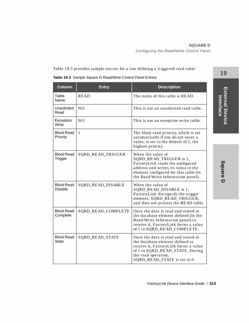
FactoryLink Device Interface Guide / 513
19
Extern
al Device
Interface
Sq
uare D
SQUARE DConfiguring the Read/Write Control Panel
Table 19-3 provides sample entries for a row defining a triggered read table:
Table 19-3 Sample Square D Read/Write Control Panel Entries
Column Entry Description
Table Name
READ The name of this table is READ.
Unsolicited Read
NO This is not an unsolicited read table.
Exception Write
NO This is not an exception write table.
Block Read Priority
1 The block read priority, which is set automatically if you do not enter a value, is set to the default of 1, the highest priority.
Block Read Trigger
SQRD_READ_TRIGGER When the value of SQRD_READ_TRIGGER is 1, FactoryLink reads the configured address and writes its value to the element configured for this table (in the Read/Write Information panel).
Block Read Disable
SQRD_READ_DISABLE When the value of SQRD_READ_DISABLE is 1, FactoryLink disregards the trigger element, SQRD_READ_TRIGGER, and does not process the READ table.
Block Read Complete
SQRD_READ_COMPLETE Once the data is read and stored in the database element defined (in the Read/Write Information panel) to receive it, FactoryLink forces a value of 1 to SQRD_READ_COMPLETE.
Block Read State
SQRD_READ_STATE Once the data is read and stored in the database element defined to receive it, FactoryLink forces a value of 1 to SQRD_READ_STATE. During the read operation, SQRD_READ_STATE is set to 0.

514 / FactoryLink Device Interface Guide
••••
SQUARE DConfiguring the Read/Write Control Panel
Block Write Priority
1 The write priority for this table is set to 1 by default.
Block Write Trigger
Since this is a read table, the elements specific to write requests are not defined.
Block Write Complete
Block Write Disable
Block Write State
Table 19-3 Sample Square D Read/Write Control Panel Entries (Continued)
Column Entry Description

FactoryLink Device Interface Guide / 515
19
Extern
al Device
Interface
Sq
uare D
SQUARE DConfiguring the Read/Write Information Panel
CONFIGURING THE READ/WRITE INFORMATION PANEL
From the Read/Write Control panel, select the row for the table you are configuring and click Next to bring the Read/Write Information panel to the foreground.
For a Read Table—Add a panel entry for each FactoryLink database element in which data read from the device will be stored when the operation executes.
For a Write Table—Add a panel entry for each element to be written when the operation executes.
Tag Name For a read table, specify a tag name for an element in which FactoryLink will store the data read from the device.
For a write table, specify a tag name for an element containing a value to be written to the device.
Valid Entry: standard element tag nameValid Data Type: digital, analog, longana, float
Tip
Alternatively, the elements you define in the Read/Write Information panel can be configured in the Tag Definition dialog in the Application Editor. Refer to the Application Editor User Guide for details.

516 / FactoryLink Device Interface Guide
••••
SQUARE DConfiguring the Read/Write Information Panel
Logical Station Enter the number representing the device from which the data is to be read or to which the element’s value will be written. This number was originally defined in the Logical Station Information panel for the logical port through which communications with this device occurs.
Valid Entry: previously defined logical station number
Data Type For each element defined in the Tag Name field, specify the type of data being read from or written to the device.
Valid Entry: register, status (default=register)
Address For a read table, enter the address in the device's memory where the value to be stored in this element is located.
For a write table, enter the address in the device's memory to which the element value will be written.
Valid Entry: 1 - 8192
Bit Offset If the element (entry in the Tag Name column) associated with this entry is digital, enter the bit offset within the word that contains the value to be read or to which the element value is to be written. Bit 1 is the most significant bit (MSB) and bit 16 is the least significant bit.
For all other FactoryLink data types, leave this field blank.
Valid Entry: 1 - 16 if data type is digital
Priority If this is an unsolicited read operation (that is, you entered YES in the Unsolicited Read field on the Read/Write Control panel), enter PRIORITY. Otherwise, accept the default of NORMAL.
Valid Entry: priority, normal (default=normal)
When the panel is complete, click Enter to validate the information. Define the data type (digital, analog, long analog, or floating-point) for any tag names displayed in the Tag Definition dialog.

FactoryLink Device Interface Guide / 517
19
Extern
al Device
Interface
Sq
uare D
SQUARE DConfiguring the Read/Write Information Panel
Table 19-4 provides sample Read/Write Information panel entries for the triggered read table defined in Table 19-3 on page 513.
Table 19-4 Sample Square D Read/Write Information Panel Entries
Field Entry Description
Table Name READ The table name defined in the Read/Write Control panel is displayed.
Tag Name REG_DIG1 When the READ table is triggered by SQRD_READ_TRIGGER (defined in the Read/Write Control panel), FactoryLink processes the table. The value read from the device is stored in REG_DIG1.
Logical Station 0 The value stored in this element is read from the Square D device configured as logical station 0.
Data Type REGISTER A register address is being read.
Address 426 The address of the register is 426.
Bit Offset 12 The bit offset containing the value being read is 12.
Priority NORMAL This read operation will be processed according to the priority specified in the Read/Write Control panel.

518 / FactoryLink Device Interface Guide
••••
SQUARE DCable Diagram
CABLE DIAGRAM
The following figure illustrates how to connect the computer running FactoryLink to a Square D device. This connection occurs from the host through an RS-232 25-pin ribbon cable to a 25-pin converter, through the converter ’s four-wire RW-422 cable to the Square D’s 9-pin port.
Figure 19-1
Host RS-232 to RS-422 converterRS-232 25-pin
Square D9-pin
FactoryLinkPin 1 is TX-
Pin 2 is TX+
Pin 3 is RX-
Pin 4 is RX+
RD-
RD+
SD-
SD+
Pins 5 and 6are jumpedtogether.
Pins 7 and 8are jumpedtogether.
RS-232 nullmodem cable

FactoryLink Device Interface Guide / 519
19
Extern
al Device
Interface
Sq
uare D
SQUARE DRun-Time Application Messages
RUN-TIME APPLICATION MESSAGES
During EDI run time, FactoryLink generates and displays messages for the Square D protocol module on the Run-Time Manager screen and, if so configured, writes them to message or analog tags. For information about configuring a message tag, see “Configuring the Logical Station Control Panel” on page 500. For information about configuring an analog tag, see “Configuring the Logical Station Information Panel” on page 504.
For information about the messages displayed for the EDI task and the format in which protocol module messages are generated, see Chapter 10, “Messages and Codes,” of this guide.
SQRD8023 Messages
SQRD8023: Error closing Multicast Service Access Point
Cause: Task was unsuccessful in closing the SAP address. This error should occur only when stopping the task.
Action: No action is required.
SQRD8023: Error sending connect command
Cause: Task was unsuccessful in sending the connect command. This command is part of initialization and terminates with this error.
Action: Device address of drop may be incorrect.
SQRD8023: Process unsolicited XMIT_ERROR
Cause: Task error attempting to process an unsolicited message.
Action: Change the format of the message sent from the PLC.
SQRD8023: Protection bit failure
Cause: Task has attempted to start, but the FactoryLink protection bit 51 could not be located.
Action: Verify that bit 51 was properly installed.

520 / FactoryLink Device Interface Guide
••••
SQUARE DRun-Time Application Messages
SQRDRCOM and SQRDSCOM Messages
If using SY/MAX point-to-point serial communications, the following messages can appear:
SQRDCPT: PPORT-%d port setup failed
Cause: Task has unsuccessfully attempted to configure the physical port indicated by the %d. This error indicates that a physical problem has occurred.
Action: Verify that the physical port is correctly defined.
SQRDCPT: Protection bit failure
Cause: Task has attempted to start, but the FactoryLink protection bit 51 could not be located.
Action: Verify that bit 51 was properly installed.
SQRDDSF: PPORT-%d start failed
Cause: Task has unsuccessfully attempted to configure the physical port indicated by the %d. This error indicates that a physical problem has occurred.
Action: Verify that the physical port is correctly defined.
SQRDRCOM, SQRDSCOM and SQRDENET Messages
Error messages in the following format can occur with the SY/MAX point-to-point serial communication or with the 802.3 Ethernet communication protocol module:
SQRDDSF: LSTA - yyy Error - xxx: sss
These errors are associated with return data to the FactoryLink EDI task and the logical port error message element. They appear in the format described in “EDI Run-Time Manager Line Format” on page 186.
The following information is also returned to the Device Message Tag element defined in the Logical Station Control panel:
SQRDDST: LSTA - yyy Error - xxx:sss
where:
yyy Is the logical station where the error occurred

FactoryLink Device Interface Guide / 521
19
Extern
al Device
Interface
Sq
uare D
SQUARE DRun-Time Application Messages
zzz Is the error number
sss Is the ASCII string describing the error message (see Table 19-5 on page 522)

SQUARE DRun-Time Application Messages
522 / FactoryLink Device Interface Guide
••••
Table 19-5 ASCII String Meanings and Descriptions
If xxx Is: sss Is an ASCII String Meaning: Description
1 Receive error An error occurred while the packet was being received.
2 Timeout Did not receive a response from the request.
3 Invalid error code Invalid error code.
4 Invalid FactoryLink type for conversion
Invalid FactoryLink element type.
5 SY/MAX error XXX XXX-SY/MAX error (see Bulletin 30598-713-01).
6 Received too many NAKs Resent the packet the retry number without receiving ACK.
7 Received unsupported Unsolicited Opcode-YYY
Received an unsupported Unsolicited Opcode-YYY.
8 Transmit error An error occurred during the transmission of the packet.

Texas Instru
men
ts
FactoryLink Device Interface Guide / 523
20
Extern
al Device
Interface
• • • •Chapter 20
Texas Instruments
This chapter contains information needed to set up and configure bidirectional communications between the FactoryLink real-time database and various devices in either of two ways:• Directly (point-to-point mode) via a COM port on the system unit• Over a TIWAY Serial Unilink network (TIWAY mode) via a COM port on the
system unit through the TIWAY Host Adapter module
The following table lists the supported device types for point-to-point and network communications:
Table 20-1 Bidirectional Communications
Point-to-Point TIWAY Serial Unilink
Texas Instruments 525 Texas Instruments 520C
Texas Instruments 530C Texas Instruments 525
Texas Instruments 530T Texas Instruments 530C
Texas Instruments 535 Texas Instruments 530T
Texas Instruments 540 Texas Instruments 535
Texas Instruments 545 PM550
Texas Instruments 565 PM550C
Texas Instruments 545
Texas Instruments 560
Texas Instruments 565
Texas Instruments RTU
Texas Instruments 5TI

524 / FactoryLink Device Interface Guide
••••
TEXAS INSTRUMENTSTexas Instruments Setup
TEXAS INSTRUMENTS SETUP
Before completing the Texas Instruments protocol module configuration panels, set up the devices as described in the following sections.
DIP Switches
Set the following switches on the Host Adapter. (See Dip Switch Settings for NITP Protocol Table.)
DIP switch 1 switch 1 upswitch 2 upswitch 3 downswitch 4 downswitch 5 configurable (See Baud Rate Table.)switch 6 configurable (See Baud Rate Table.)switch 7 configurable (See Baud Rate Table.)switch 8 configurable (See Baud Rate Table.)switch 9 configurable (See Host Command Timeout Table.)switch 10 configurable (See Host Command Timeout Table.)
DIP switch 2 switch 1 upswitch 2 downswitch 3 upswitch 4 downswitch 5 configurable (See Baud Rate Table.)switch 6 configurable (See Baud Rate Table.)switch 7 configurable (See Baud Rate Table.)switch 8 configurable (See Baud Rate Table.)switch 9 downswitch 10 down

FactoryLink Device Interface Guide / 525
Texas Instru
men
ts
20
Extern
al Device
Interface
TEXAS INSTRUMENTSTexas Instruments Setup
Figure 20-1 DIP Switch Settings for the NITP Protocol
1 2 3 4 5 6 7 8 9 10UP Dipswitch 1
Host Command timeoutTIWAY I Baud Rate
Up SynchronousDown Asynchronous
Up Full DuplexDown Half Duplex
Up NRZIDown NRZ
Up NITP
1 2 3 4 5 6 7 8 9 10UP Dipswitch 2
Up Test ModeDown Run Mode
Up HIU/EHA &IO Loop Test
Down MHIU/EHA
Host Port Baud Rate
Up SynchronousDown Asynchronous
Up Full DuplexDown Half Duplex
Up Even ParityDown Odd Parity
Up Parity Enabled
Dipswitch Settings for NITP Protocol

526 / FactoryLink Device Interface Guide
••••
TEXAS INSTRUMENTSTexas Instruments Setup
Baud Rate
Set the TIWAY Serial Unilink network baud rate with DIP switch 1 switches 5, 6, 7, and 8. Set the host PC’s (PC running FactoryLink) port baud rate with DIP switch 2 switches 5, 6, 7, and 8. Baud rates for the TIWAY Serial Unilink network and the host PC’s port may be configured differently.
Use Figure 20-2 to set the baud rate on DIP switches 1 and/or 2:
Figure 20-2 DIP Switch Baud Rates
Up Down 1 0
Switches Baud Rate
0 1 0 00 1 0 10 1 1 00 1 1 11 0 0 01 0 0 11 0 1 01 0 1 11 1 0 01 1 0 11 1 1 01 1 1 1
110150300600
1200240048009600
1920038400
57600*115200*
0 = Down 1 = Up
*These values are not available on the Host Port

FactoryLink Device Interface Guide / 527
Texas Instru
men
ts
20
Extern
al Device
Interface
TEXAS INSTRUMENTSTexas Instruments Setup
Timeout
Use Figure 20-3 to set the host PC’s command timeout:
Figure 20-3 Host Command Timeout Table
DIPSWITCH 1
Position
9 10 Description
Down Down 0 sec - Accepts NoHost Commands (SANM)
Down Up 10 sec Timeout
Up Down 20 sec Timeout
Up Up 40 sec Timeout

528 / FactoryLink Device Interface Guide
••••
TEXAS INSTRUMENTSTexas Instruments Setup
DIP Switches for TIWAY NIM
Use Figure 20-4 to set DIP switches for each NIM:
Figure 20-4 Dipswitch Settings for TIWAY NIM
Note
If changing the baud rate of the TIWAY Serial Unilink network, change the corresponding switches for the Host Adapter.
Dipswitch Settings for TIWAY NIM
Switch Desired Setting
LOCAL/REMOTE REMOTE (ONLINE)
KEYDELAY OFFLCKBIT OFFNRZI/NRZ NRZIX.25/HDLC HDLCFULL/HALF HALFSYNC/ASYNC ASYNCBAUD 115.2KNETWORK ADDRESS 1-254 ARE VALID ADDRESSES

FactoryLink Device Interface Guide / 529
Texas Instru
men
ts
20
Extern
al Device
Interface
TEXAS INSTRUMENTSAccessing the Texas Instruments Tables
ACCESSING THE TEXAS INSTRUMENTS TABLES
When you choose Texas Instruments TIWAY/Point-to-Point from the Configuration Manager Main Menu, the Texas Instruments configuration panels are displayed.
Note
Before completing the protocol-specific Texas Instruments configuration panels, you must complete the External Device Definition panel. See “Identifying Protocol Types and Defining Logical Ports” on page 70 for details.

530 / FactoryLink Device Interface Guide
••••
TEXAS INSTRUMENTSConfiguring the Unilink Setup Table
CONFIGURING THE UNILINK SETUP TABLE
To bring the Unilink Setup panel to the foreground, click on its title bar in the display of all configuration panels.
If you are communicating directly (point-to-point) with a single TI PLC, you do not need to configure this table.
Specify the following information:
Logical Port forUNILINK
Enter a number, defined in the External Device Definition panel Logical Port column, to represent a particular communication path to a TI device.
Valid Entry: previously defined logical port number
Comment Enter reference information about this logical station.
Valid Entry: alphanumeric string of up to 31 characters
When the panel is complete, choose Next.

FactoryLink Device Interface Guide / 531
Texas Instru
men
ts
20
Extern
al Device
Interface
TEXAS INSTRUMENTSConfiguring the Unilink Setup Table
Table 20-2 provides sample entries for the Texas Instruments TIWAY Unilink Setup panel:
From the Unilink Setup panel, select the row for the logical port you are configuring and click on Next to bring the Unilink Setup Information panel to the foreground.
Specify the following information:
Adapter Mode Specify whether a Host Adapter is the network manager.
MHIU Network Manager
HIU Any other Host Adapter on the network
Table 20-2 Sample Texas Instruments TIWAY Unilink Setup Panel Entries
Field Entry Description
Logical Port for UNILINK
0 Specifies the logical communication path configured by this table
Comment Port 1 as MHIU Port 1 communicates with a TIWAY Host Adapter

532 / FactoryLink Device Interface Guide
••••
TEXAS INSTRUMENTSConfiguring the Unilink Setup Table
Adapter Station Enter the address of a Host Adapter on a network. Each Host Adapter on a TIWAY network must have a unique address.
Valid Entry: 1 - 254
Adapter MaxStation Address
Enter the number of the highest physical station address on the TIWAY Serial Unilink network associated with a logical station specified in the Texas Instruments Logical Station Table.
Valid Entry: 1 - 254
NM Option 1through NM
Option E
(Optional) Thirteen fields that allow you to configure optional parameters for an MHIU Host Adapter. For a description of these optional parameters, refer to the section on configuring the network manager in the TIWAY 1 UNILINK Host Adapter User’s Manual.
Valid Entry: Refer to the section on configuring the MHIU command in the TIWAY 1 UNILINK Host Adapter User’s Manual (default=0)
HIU Option 1through HIU
Option 3
(Optional) Three fields that allow you to configure optional parameters for an HIU Host Adapter. For more information about optional parameters for this field, refer to the section on configuring the HIU in the TIWAY 1 UNILINK Host Adapter User’s Manual.
Valid Entry: Refer to the section on configuring the HIU in the TIWAY 1 UNILINK Host Adapter User’s Manual. (default=0)
When the panel is complete, choose Next.

FactoryLink Device Interface Guide / 533
Texas Instru
men
ts
20
Extern
al Device
Interface
TEXAS INSTRUMENTSConfiguring the Unilink Setup Table
Table 20-3 provides sample entries for the Texas Instruments TIWAY Unilink Setup Information panel:
Table 20-3 Sample Texas Instruments TIWAY Unilink Setup Information Panel Entries
Field Entry Description
Adapter Mode MHIU Host Adapter is configured for MHIU mode
Adapter Station 5 Address for Host Adapter on the network
Adapter Max Station Address
1 The highest NIM address on the network is 1
NM Option 1 - 9, A-E 1 Not configured because the Host Adapter is configured in MHIU mode
HIU Option 1-3 0

534 / FactoryLink Device Interface Guide
••••
TEXAS INSTRUMENTSConfiguring the Logical Station Control Panel
CONFIGURING THE LOGICAL STATION CONTROL PANEL
To bring the Logical Station Control panel to the foreground, click on its title bar in the display of all configuration panels.
Complete a row for each logical port specified in the External Device Definition panel you want to define as a communication path for read and write operations.
Logical Port Enter a number, defined in the External Device Definition panel Logical Port column, to represent a particular communication path to a TI device.
Valid Entry: previously defined logical port number
Baud Rate Enter the speed at which the protocol module communicates with the devices linked to FactoryLink via this logical port. This entry must match the baud rate configuration of the devices. Refer to the device manufacturers documentation for details.
Valid Entry: 110, 150, 300, 600, 1200, 2400, 3600, 4800, 7200, 9600, 19200 (default=9600)
Recommended entry is 19200 if using a TI PLC on a TIWAY network or 9600 if using a point-to-point TI PLC. However, if using hardware requiring special parameters, you may need to enter a different baud rate.

FactoryLink Device Interface Guide / 535
Texas Instru
men
ts
20
Extern
al Device
Interface
TEXAS INSTRUMENTSConfiguring the Logical Station Control Panel
Parity Enter the parity error correction during transmission via this logical port. This entry must match the configuration of the devices communicating via this port. Refer to the device manufacturers documentation for details.
Valid Entry: odd, even, none
Data Bits Enter the number of data bits used during transmission via this logical port. This entry must match the configuration of the devices communicating via this port. Refer to the device manufacturers documentation for details.
Valid Entry: 5, 6, 7, 8
The recommended entry is 7. However, if using hardware requiring special parameters, you may need to enter a different data bit.
Stop Bits Enter the number of bits sent after a character to create a pause before the start of the next character. This entry must match the configuration of the devices communicating via this port. Refer to the device manufacturers documentation for details.
Valid Entry: 1, 2
The recommended entry is 1. However, if using hardware requiring special parameters, you may need to enter a different stop bit.
Timeout Enter the length of time, in tenths of a second, the protocol module will wait to receive a response to a read or write command before timing out. You must enter a value greater than 0 for the protocol module to timeout.
Valid Entry: 0 - 32000
Error MsgTag Name
(Optional) Enter a tag name for a message element to which a text string will be written to indicate a communications error associated with this logical port.
Valid Entry: standard element tag nameValid Data Type: message
When the panel is complete, click on Enter to validate the information. Define the data type (message) for any tag names displayed in the Tag Definition dialog.

536 / FactoryLink Device Interface Guide
••••
TEXAS INSTRUMENTSConfiguring the Logical Station Control Panel
Table 20-4 provides sample entries for the Texas Instruments Logical Station Control panel:
Table 20-4 Sample Texas Instruments Logical Station Control Panel Entries
Field Entry Description
Logical Port 0 Specifies the logical communication path configured by this table.
Baud Rate 9600 Specifies the communication rate.
Parity ODD Odd parity checking.
Data Bits 7 Specifies 7 data bits in the transmission.
Stop Bits 1 Specifies 1 stop bit in the transmission.
Timeout 30 The response timeout is 3 seconds.
Status Msg Tag TI_LPORT0_MSG Error messages are written to the message element logical port 0.

FactoryLink Device Interface Guide / 537
Texas Instru
men
ts
20
Extern
al Device
Interface
TEXAS INSTRUMENTSConfiguring the Logical Station Information Panel
CONFIGURING THE LOGICAL STATION INFORMATION PANEL
From the Logical Station Control panel, select the row for the logical port you are configuring and click on Next to bring the Logical Station Information panel to the foreground.
Complete a row for each device to communicate through this logical port.
Error/Status TagName
(Optional) Enter a tag name for an analog element in which to store communications error codes associated with this device (logical station).
You can animate output-text objects to display the codes stored in an Error/Status Tag Name element on a graphics screen. Refer to the Application Editor User Guide for more information.
Valid Entry: standard element tag nameValid Data Type: analog
Logical Station Enter a number to identify the logical station to which the information in this row pertains. A logical station represents the combination of a logical port with a physical station. Assign a unique number to each device communicating through this logical port.

538 / FactoryLink Device Interface Guide
••••
TEXAS INSTRUMENTSConfiguring the Logical Station Information Panel
You will later enter this logical station number in a read or write table to represent the device defined in this row. In a read or write table, this number will identify the device to or from which data is to be sent or received.
Valid Entry: 0 - 999
Device Type Enter the TI PLC type to which communications are to be directed. (When using a TI545, enter TWY565 or PLC 565.)
Physical Station Physical station address of the device with which the EDI task communicates when using this logical station in a Read/Write table.
Valid Entry: 1 - 254 (Normally, the physical station number is the same as the logical station number.)
Comment (Optional) Enter reference information about this logical station.
Valid Entry: alphanumeric string of up to 31 characters
When the panel is complete, click on Enter to validate the information. Define the data type (analog) for any tag names displayed in the Tag Definition dialog.
Valid Entry Unilink Network
TWY520C PLC525
TWY525 PLC530C
TWY530C PLC530T
TWY530T PLC535
TWY535 PLC540
TWY560 PLC565
TWY565
TWYRTU
TWY5TI
TWY550 (indicates PM550)
TWY550C (indicates PM550C)

FactoryLink Device Interface Guide / 539
Texas Instru
men
ts
20
Extern
al Device
Interface
TEXAS INSTRUMENTSConfiguring the Logical Station Information Panel
Table 20-5 provides sample entries for the Texas Instruments Logical Station Information panel:
Table 20-5 Sample Texas Instruments Logical Station Information Panel Entries
Field Entry Description
Error/Status Tag Name TI_STATION0_STATUS
Contains information about communication errors
Logical Station 0 Specifies the logical communication paths.
Device Type TWY565 Specifies the type of device connected to the communication path.
Physical Station 1 Specifies the physical station numbers associated with the logical path.
Comment TI, PORT 0

540 / FactoryLink Device Interface Guide
••••
TEXAS INSTRUMENTSConfiguring the Read/Write Control Panel
CONFIGURING THE READ/WRITE CONTROL PANEL
To bring the Read/Write Control panel to the foreground, click on its title bar in the display of all configuration panels or click on Next from the Logical Station Information panel.
Note
If using the loop indexing feature, refer to “Configuring Tables for Loop Indexing” on page 554 before configuring any Read/Write tables.

FactoryLink Device Interface Guide / 541
Texas Instru
men
ts
20
Extern
al Device
Interface
TEXAS INSTRUMENTSConfiguring the Read/Write Control Panel
Complete a row for each read or write table.
Table Name Give this read or write request a name. Define one request (table) per line and do not include spaces in the name. You can define as many tables in this panel as available memory allows. Try to make the table name reflective of the operation it represents.
If this is a triggered read or a block write table, when the trigger element (Block Read Trigger for a read operation or Block Write Trigger for a write operation) is forced to 1 (ON), the element prompts FactoryLink to process this table and any other table in which the same trigger is defined.
Valid Entry: alphanumeric string of up to 16 characters
ExceptionWrite
For EDI to interpret this operation as a triggered block write or as a read operation, accept the default of NO.
For EDI to interpret this operation as an exception write and write element values to the device only when those values change, enter YES. Do not specify elements expected to change at frequent and unpredictable intervals in an exception write table. Any element specified will be written to the device in its own packet (message) each time it changes. Defining elements that change value frequently as exception writes can slow down communications or result in an error message.
In an exception write, an internal change-status indicator within the element containing the data to be written prompts the write operation. If an element is configured for an exception write and EDI recognizes this indicator has been set since the last scan of the real-time database (indicating the value of the element has changed), EDI writes this element’s value to the device.
Valid Entry: yes, no (default = no)
Tip
Refer to Chapter 8, “Application Design Tips and Techniques,” for information about triggering schemes using elements defined in this panel.

542 / FactoryLink Device Interface Guide
••••
TEXAS INSTRUMENTSConfiguring the Read/Write Control Panel
Block Read Priority If this is a block read operation, enter a number to indicate the priority of this table, relative to other read operations. The highest priority is 1. This number influences the order in which the EDI task handles the queuing of block read requests. If EDI receives two requests at the same time, it processes the request with the highest priority first. The default is 1.
If this is a write operation, accept the default of 1. This field defaults to 1 regardless of whether the operation being defined is a block read.
Valid Entry: 1 - 4 (default = 1)
Block ReadTrigger
If this is a write operation, ignore this field.
If this is a triggered read operation, this field is required. Enter a tag name for a digital element to initiate a block read of the addresses specified in the Read/Write Information panel. When this element’s value is forced to 1 (ON), the addresses are read.
Valid Entry: standard element tag nameValid Data Type: digital
Note
The Block Read Trigger, Block Read Disable, Block Read Complete, and Block Read State elements apply only to triggered read operations. Do not define these elements for write operations.
Tip
The Block Read Disable element can be used to disable a block read operation that is either part of a cascaded loop or is self-triggered. The triggering cycle will cease upon disabling, however. To re-enable a cascaded loop or a self-triggered read table, the Block Read Trigger element must be toggled or forced to 1. Refer to Chapter 8, “Application Design Tips and Techniques,” for details.

FactoryLink Device Interface Guide / 543
Texas Instru
men
ts
20
Extern
al Device
Interface
TEXAS INSTRUMENTSConfiguring the Read/Write Control Panel
Block ReadDisable
If this is a write operation, ignore this field.
If this is a triggered read operation, this field is optional. If you need a digital element to disable a block read of the elements specified in this table, enter a tag name. When this tag’s value is forced to 1 (ON), the read operation is not executed, even when the block read trigger is set to 1.
To re-enable a block read table that has been disabled, set this element back to 0 (OFF).
Valid Entry: standard element tag nameValid Data Type: digital
Block ReadComplete
If this is a write operation, ignore this field.
If this is a triggered read operation, this field is optional. If you need a digital element to indicate when this operation is complete, enter a tag name. This element is forced to 1 (ON) at startup. After the elements defined in the Read/Write Information panel have been updated in the FactoryLink database, the complete element is forced to 1 again.
Do not use this element when more than one logical port is specified in a single table.
Valid Entry: standard element tag nameValid Data Type: digital
Block Read State If this is a write operation, ignore this field.
If this is a triggered read operation, this field is optional. If you need a digital element to indicate the state of this operation (in progress or complete), enter a tag name. This element is forced to 1 (ON) at startup. While the table is being processed, the element is set to 0 (OFF). After the elements defined in the Read/Write Information panel have been updated in the FactoryLink database, the state element is forced back to 1.
Valid Entry: standard element tag nameValid Data Type: digital

544 / FactoryLink Device Interface Guide
••••
TEXAS INSTRUMENTSConfiguring the Read/Write Control Panel
Block WritePriority
If this is a block or exception write operation, enter a number to indicate the priority of this table, relative to other write operations. The highest priority is 1. This number influences the order in which the EDI task handles the queuing of write requests. If EDI receives two requests at the same time, it processes the request with the highest priority first. The default is 1.
If this is a read operation, accept the default of 1. This field defaults to 1 regardless of whether the operation being defined is a block or exception write.
Valid Entry: 1 - 4 (default = 1)
Block Write Trigger If this is a read operation or an exception write operation you do not plan to periodically disable, ignore this field.
If this is a block write table or an exception write table you plan to periodically disable, this field is required. Enter a tag name for a digital element to initiate a block write of the element values specified in the Read/Write Information panel to the addresses defined to receive the values. When this element’s value is forced to 1 (ON), FactoryLink writes the values.
Valid Entry: standard element tag nameValid Data Type: digital
Note
The Block Write Trigger, Block Write Disable, Block Write Complete, and Block Write State elements apply only to write operations. Do not define these elements for read operations.
Tip
The Block Write Disable element can be used to disable a block write operation that is either part of a cascaded loop or is self-triggered. The triggering cycle will cease upon disabling, however. To re-enable a cascaded loop or a self-triggered write table, the Block Write Trigger element must be toggled or forced to 1. Refer to Chapter 8, “Application Design Tips and Techniques,” for details.

FactoryLink Device Interface Guide / 545
Texas Instru
men
ts
20
Extern
al Device
Interface
TEXAS INSTRUMENTSConfiguring the Read/Write Control Panel
Block WriteDisable
If this is a read operation or an exception write operation you do not plan to periodically disable, ignore this field.
If this is a block write table or an exception write table you plan to periodically disable, this field is optional. Enter a tag name for a digital element to disable a block write to the addresses specified in this table. When this tag’s value is forced to 1 (ON), the write operation is not executed, even when the block write trigger is set to 1.
To re-enable a block write table that has been disabled, set this element back to 0 (OFF).
Valid Entry: standard element tag nameValid Data Type: digital
Block WriteComplete
If this is a read or exception write operation, ignore this field.
If this is a block write table, this field is optional. If you need a digital element to indicate when this operation is complete, enter a tag name. This element is forced to 1 (ON) at startup. After the data defined in this table’s Read/Write Information panel has been written to the device, the complete element is forced to 1 again.
Do not use this element when more than one logical port is specified in a single table.
Valid Entry: standard element tag nameValid Data Type: digital
Block Write State If this is a read or exception write operation, ignore this field.
If this is a block write operation, this field is optional. If you need a digital element to indicate the state of this operation (in progress or complete), enter a tag name. This element is forced to 1 (ON) at startup. While the table is being processed, the element is set to 0 (OFF). After the data defined in this table’s Read/Write Information panel has been written to the device, the state element is forced back to 1.
Do not use this element when more than one logical port is specified in a single table.
Valid Entry: standard element tag nameValid Data Type: digital
When the panel is complete, click on Enter to validate the information. Define the data type (digital) for any tag names displayed in the Tag Definition dialog.

546 / FactoryLink Device Interface Guide
••••
TEXAS INSTRUMENTSConfiguring the Read/Write Control Panel
Table 20-6 provides sample entries for the Texas Instruments Read/Write Control panel:
Table 20-6 Sample Texas Instruments Read/Write Control Panel Entries
Field Entry Description
Table Name READ Name of the read/write table.
Exception Write N Table READ will perform exception writes.
Block Read Priority 1 Priority is set to 1.
Block Read Trigger TI_READ_TRIGGER When the value of TI_READ_TRIGGER is 1 or (on), a block read of values specified by the Read/Write Information panel associated with table READ occurs.
Block Read Disable TI_READ_DISABLE The element TI_READ_DISABLE disables the block read of table READ when the value is 1.
Block Read State TI_READ_STATE The value for TI_READ_STATE is set to 1 if a read operation of table READ is in progress, and the value is 0 if it is inactive.
Block Write Priority 1 Default=1
Block Write Trigger
Block Write State

FactoryLink Device Interface Guide / 547
Texas Instru
men
ts
20
Extern
al Device
Interface
TEXAS INSTRUMENTSConfiguring the Read/Write Information Panel
CONFIGURING THE READ/WRITE INFORMATION PANEL
From the Read/Write Control panel, select the row for the table you are configuring and click on Next to bring the Read/Write Information panel to the foreground.
For a Read Table—Add a panel entry for each FactoryLink database element in which data read from the device will be stored when the operation executes.
For a Write Table—Add a panel entry for each element to be written when the operation executes.
Tip
Alternatively, the elements you define in the Read/Write Information panel can be configured in the tag definition dialog in the Application Editor. Refer to the Application Editor User Guide for details.

548 / FactoryLink Device Interface Guide
••••
TEXAS INSTRUMENTSConfiguring the Read/Write Information Panel
Tag Name For a read table, specify a tag name for an element in which FactoryLink will store the data read from the device.
For a write table, specify a tag name for an element containing a value to be written to the device.
Valid Entry: standard element tag nameValid Data Type: digital, analog, float
Logical Station Enter the number representing the device from which the data is to be read or to which the element’s value will be written. This number was originally defined in the Logical Station Information panel for the logical port through which communications with this device occurs.
Valid Entry: previously defined logical station number
Data Type Specify the type of data being read from or written to the device for each element defined in the Tag Name field. Refer to the TIWAY 1 UNILINK Host Adapter User’s Manual for valid data types for each channel. If using the loop indexing feature, refer to “Configuring Tables for Loop Indexing” on page 554 for information about valid entries for this field.
Valid Entry FactoryLink Type
NONE - (default) No data type
V - variable memory Analog
K - constant memory Analog
X - X input packed Digital
Y - Y input packed Digital
C - CR packed Digital
WX - word input Analog
WY - word output Analog
TCP - timer counter preset Analog
TCC - timer counter current Analog
DSP - drum step preset Analog

FactoryLink Device Interface Guide / 549
Texas Instru
men
ts
20
Extern
al Device
Interface
TEXAS INSTRUMENTSConfiguring the Read/Write Information Panel
TI 545 or TI 565 PLCs with s-memory (special-function memory) can also use the following entries:
DSC - drum step current Analog
DCP - drum count preset Analog
STW - status word Analog
Valid Entry FactoryLink Type
Valid Entry Description FactoryLink
Type
** LVF Loop V-flags Analog
** LRSF Loop ramp/soak status Analog
*** AVF Analog alarm V-flags Analog
AACF Analog alarm C-flags Floating-point
LCF Loop C-flags Floating-point
LKC Loop gain Floating-point
LTI Loop reset Floating-point
LTD Loop rate Floating-point
LHA Loop high alarm Floating-point
LLA Loop low alarm Floating-point
LPV Loop process variable Floating-point
LPVH Loop pv high limit Floating-point
LPVL Loop pv low limit Floating-point
*
*****
Read-only. For point-to-point protocol modules, use AVF_ instead of AVF.Read-only.Exception write only.

550 / FactoryLink Device Interface Guide
••••
TEXAS INSTRUMENTSConfiguring the Read/Write Information Panel
LODA Loop orange deviation Floating-point
LYDA Loop yellow deviation Floating-point
LTS Loop sample rate Floating-point
LSP Loop setpoint Floating-point
LMN Loop output Floating-point
** LERR Loop error Floating-point
LMX Loop bias Floating-point
LHHA Loop high alarm limit Floating-point
LLLA Loop low alarm limit Floating-point
LRCA Loop rate of change limit Floating-point
LRDS Loop ram dest. setpoint Floating-point
LRRC Loop ramp rate of change Floating-point
LRST Loop soak time Floating-point
LSDB Loop soak deadband Floating-point
AHA Analog alarm high limit Floating-point
ALA Analog alarm low limit Floating-point
APV Analog alarm process variable
Floating-point
APVH Analog alarm PV high limit Floating-point
APVL Analog alarm PV low limit Floating-point
Valid Entry Description FactoryLink
Type
*
*****
Read-only. For point-to-point protocol modules, use AVF_ instead of AVF.Read-only.Exception write only.

FactoryLink Device Interface Guide / 551
Texas Instru
men
ts
20
Extern
al Device
Interface
TEXAS INSTRUMENTSConfiguring the Read/Write Information Panel
AODA Analog alarm orange deviation
Floating-point
AYDA Analog alarm yellow deviation
Floating-point
ATS Analog alarm sample rate Floating-point
ASP Analog alarm setpoint Floating-point
** AERR Analog alarm error Floating-point
AHHA Analog alarm high limit Floating-point
ALLA Analog alarm low limit Floating-point
ARCA Analog alarm rate of change Floating-point
LCFH Analog C flags high order Analog
LCFL Analog C flags low order Analog
ACFH Analog C flags high order Analog
ACFL Analog C flags low order Analog
*** PORT Port ON/OFF element type Digital
Valid Entry Description FactoryLink
Type
*
*****
Read-only. For point-to-point protocol modules, use AVF_ instead of AVF.Read-only.Exception write only.

552 / FactoryLink Device Interface Guide
••••
TEXAS INSTRUMENTSConfiguring the Read/Write Information Panel
Address Enter the address of the memory location (word) being read or written to. The system reads the value at the address and transfers it to the element specified in the Tag Name column. The amount of memory assigned to each PLC data type depends on several factors, including the PLC model and the amount of memory installed in the system. If not using the loop indexing feature, do not configure more than one Read/Write table to write to the same address.
If using the loop indexing feature, the Address field may need to be left blank. Refer to “Loop Indexing” on page 554 for information about configuring tables for loop indexing.
DCP, LRDS, LRRC, LRST, and LSDB data types require you employ additional parameters to determine the Address field entry. Refer to “Additional Parameters for TI Data Types” on page 564 for information about these parameters.
Valid Entry: 1 - 32767, 1 - 64 (used with TI 545 or TI 565 PLCs with s-memory; see additional data types listed in the preceding table)
Loop Index If not using loop indexing, leave this field blank.
(Optional; use only with TI 545 or TI 565 PLCs having s-memory) Alphanumeric string representing an analog element whose value determines the loop element. The system reads the PLC address specified in the Logical Station and Data Type fields and writes the returned data to the loop element specified by the value of the loop index variable. The value of this loop index variable designates one of the elements specified in the Tag Name field. The loop index variable is valid only for s-memory data types such as loop variable and analog alarms.
Note
Use the PORT data type only with an exception write element. A 1 (one) written to this element closes the port associated with the logical station for this element. No further reads or writes occur. A 0 (zero) written to this element opens the port. Use of the TIWAY Network reinitializes the Unilink Host Adapter before further reads or writes occur. After the port is reopened, reads and writes will operate normally.

FactoryLink Device Interface Guide / 553
Texas Instru
men
ts
20
Extern
al Device
Interface
TEXAS INSTRUMENTSConfiguring the Read/Write Information Panel
Refer to the Data Type field description on page 548 for valid s-memory data types. Refer to “Configuring Tables for Loop Indexing” on page 554 for more information about loop indexing.
Valid Entry: NONE, LOOP1, LOOP2, LOOP3, LOOP4, LOOP5, LOOP6, LOOP7, LOOP8, LOOP9, LOOP10, LOOP11, LOOP12, LOOP13, LOOP14, LOOP15, LOOP16 (default = NONE)
When the panel is complete, click on Enter to validate the information. Define the data type (digital, analog, or floating-point) for any tag names displayed in the Tag Definition dialog.
Table 20-7 provides sample entries for the Texas Instruments Read/Write Information panel:
Table 20-7 Sample Texas Instruments Read/Write Information Panel Entries
Field Entry Description
Table Name READ Specifies the Read/Write table name
Tag Name TX_DIG_01 Destination elements in the real-time database for the addresses read from the PLC
Logical Station 0 Specifies the path to send the request
Data Type Y Variables in memory addresses 1 and 50
Address 1 Memory addresses
Loop Index NONE

554 / FactoryLink Device Interface Guide
••••
TEXAS INSTRUMENTSLoop Indexing
LOOP INDEXING
You can configure a TI PLC to read and write to up to 64 loop elements in the FactoryLink real-time database using a loop index variable.
A loop index variable is an analog element whose value specifies which of up to 64 elements (loop elements) in the real-time database that it will read or write to.
Up to 16 loop index variables can be defined. These loop index variables constitute a loop index.
Configuring Tables for Loop Indexing
To implement the loop indexing option, configure the following tables:• One initial Read/Write table that references up to 16 loop index variables• One or more Read/Write tables that reference the loop index variables specified
in the initial Read/Write table and defined in the Application Editor task
Initial Read/Write Table
First, configure one Texas Instruments Read/Write table that references up to 16 loop index variables.
Next, to implement the loop indexing option, in the Texas Instruments Read/Write Control panel, configure either a write trigger or enable the exception write.
The entries in the loop indexing Texas Instruments Read/Write Information panel identify the analog loop index variables. The panel can include up to 16 loop index variables. The value of each loop index variable specifies a different loop element in the FactoryLink real-time database. Configure only one Texas Instruments Read/Write Information panel to identify these loop index variables.
Specify the following information for each loop index variable:
Tag Name (Optional) Enter a tag name for an analog element in which to store communications error codes associated with this device (logical station).
You can animate output-text objects to display the codes stored in an Error/Status Tag Name element on a graphics screen. Refer to the Application Editor User Guide for more information.
Valid Entry: standard element tag nameValid Data Type: analog

FactoryLink Device Interface Guide / 555
Texas Instru
men
ts
20
Extern
al Device
Interface
TEXAS INSTRUMENTSLoop Indexing
Logical Station Enter a number to identify the logical station to which the information in this row pertains. A logical station represents the combination of a logical port with a physical station. Assign a unique number to each device communicating through this logical port.
You will later enter this logical station number in a read or write table to represent the device defined in this row. In a read or write table, this number will identify the device to or from which data is to be sent or received.
Valid Entry: 0 - 999
Data Type Specify the type of data being read from or written to the device for each element defined in the Tag Name field.
Valid Entry: register, status
Address For a read table, enter the address in the device’s memory where the value to be stored in this element is located.
For a write table, enter the address in the device’s memory to which the element value will be written.
Valid Entry: 1 - 8192
Loop Index Enter an alphanumeric string representing a real-time database analog element whose value determines the TI 545 or TI 565 loop element. Loop index variable used only with TI 545 or TI 565 PLCs having s-memory.
Valid Entry: NONE, LOOP1, LOOP2, LOOP3, LOOP4, LOOP5, LOOP6, LOOP7, LOOP8, LOOP9, LOOP10, LOOP11, LOOP12, LOOP13, LOOP14, LOOP15, LOOP16, (default = NONE)

556 / FactoryLink Device Interface Guide
••••
TEXAS INSTRUMENTSLoop Indexing
When all appropriate information has been specified, the panel should resemble the following panel:
In this example, table FB references the 16 loop elements (listed in the Tag Name field) previously defined in the Graphics Mode Input task. The entries in the Loop Index field reference the loop elements in the Tag Name field that are used by the loop indexing Read/Write tables. For example, if a loop indexing Read/Write table needs to reference the analog value contained in the element LOOPNDX1, you must enter LOOP1 in its Loop Index field.
When the Texas Instruments Read/Write table is complete, choose Enter to accept the information.
Loop Indexing Read/Write Table
Next, configure one or more Read/Write tables for each loop index variable defined in the initial Read/Write table.
The entries in the loop indexing Texas Instruments Read/Write Information panel reference each loop index variable referenced in the initial Read/Write table and the corresponding loop elements read by this variable. These entries also use the loop index variable specified in the initial Read/Write table to identify loop elements in the FactoryLink real-time database to be read or written to. The panel can include up to 1,000 entries.

FactoryLink Device Interface Guide / 557
Texas Instru
men
ts
20
Extern
al Device
Interface
TEXAS INSTRUMENTSLoop Indexing
Specify the following information for each loop element:
Tag Name For a read table, specify a tag name for an element in which FactoryLink will store the data read from the device.
For a write table, specify a tag name for an element containing a value to be written to the device.
Valid Entry: standard element tag nameValid Data Type: digital, analog, floating-point
Logical Station Enter the number representing the device from which the data is to be read or to which the element’s value will be written. This number was originally defined in the Logical Station Information panel for the logical port through which communications with this device occurs.
Valid Entry: previously defined logical station number
Data Type Specify the type of data being read from or written to the device for each element defined in the Tag Name field.
For valid data types for each channel, refer to the TIWAY 1 UNILINK Host Adapter User’s Manual.
Valid Entry Description FactoryLink Type
V Variable memory Analog
K Constant memory Analog
X X input packed Digital
Y Y input packed Digital
C CR packed Digital
WX Word input Analog
WY Word output Analog
TCP Timer counter preset Analog
TCC Timer counter current Analog
DSP Drum step preset Analog

558 / FactoryLink Device Interface Guide
••••
TEXAS INSTRUMENTSLoop Indexing
TI 545 or TI 565 PLCs with s-memory (special-function memory) can also use the following entries:
DSC Drum step current Analog
DCP3 Drum count preset Analog
STW Status word Analog
Valid Entry Description FactoryLink Type
Valid Entry Description FactoryLink Type
** LVF Loop V-flags Analog
** LRSF Loop ramp/soak status Analog
*** AVF Analog alarm V-flags Analog
AACF Analog alarm C-flags Floating-point
LCF Loop C-flags Floating-point
LKC Loop gain Floating-point
LTI Loop reset Floating-point
LTD Loop rate Floating-point
LHA Loop high alarm Floating-point
LLA Loop low alarm Floating-point
LPV Loop process variable Floating-point
LPVH Loop pv high limit Floating-point
*
*****
Read-only. For point-to-point protocol modules, use AVF_ instead of AVF.Read-only.Exception write only.

FactoryLink Device Interface Guide / 559
Texas Instru
men
ts
20
Extern
al Device
Interface
TEXAS INSTRUMENTSLoop Indexing
LPVL Loop pv low limit Floating-point
LODA Loop orange deviation Floating-point
LYDA Loop yellow deviation Floating-point
LTS Loop sample rate Floating-point
LSP Loop setpoint Floating-point
LMN Loop output Floating-point
** LERR Loop error Floating-point
LMX Loop bias Floating-point
LHHA Loop high alarm limit Floating-point
LLLA Loop low alarm limit Floating-point
LRCA Loop rate of change limit
Floating-point
LRDS Loop ram dest. setpoint
Floating-point
LRRC Loop ramp rate of change
Floating-point
LRST Loop soak time Floating-point
LSDB Loop soak deadband Floating-point
AHA Analog alarm high limit
Floating-point
Valid Entry Description FactoryLink Type
*
*****
Read-only. For point-to-point protocol modules, use AVF_ instead of AVF.Read-only.Exception write only.

560 / FactoryLink Device Interface Guide
••••
TEXAS INSTRUMENTSLoop Indexing
ALA Analog alarm low limit
Floating-point
APV Analog alarm process variable
Floating-point
APVH Analog alarm PV high limit
Floating-point
APVL Analog alarm PV low limit
Floating-point
AODA Analog alarm orange deviation
Floating-point
AYDA Analog alarm yellow deviation
Floating-point
ATS Analog alarm sample rate
Floating-point
ASP Analog alarm setpoint Floating-point
** AERR Analog alarm error Floating-point
AHHA Analog alarm high limit
Floating-point
ALLA Analog alarm low limit
Floating-point
ARCA Analog alarm rate of change
Floating-point
LCFH Loop C flags high order
Analog
Valid Entry Description FactoryLink Type
*
*****
Read-only. For point-to-point protocol modules, use AVF_ instead of AVF.Read-only.Exception write only.

FactoryLink Device Interface Guide / 561
Texas Instru
men
ts
20
Extern
al Device
Interface
TEXAS INSTRUMENTSLoop Indexing
Address For a read table, enter the address in the device’s memory where the value to be stored in this element is located.
For a write table, enter the address in the device’s memory to which the element value will be written.
If no loop index variables have yet been specified, when used with the loop indexing feature, this field acts as a default address for the real-time database to write to at startup.
LCFL Loop C flags low order Analog
ACFH Analog C flags high order
Analog
ACFL Analog C flags low order
Analog
*** PORT Port ON/OFF digital element
Digital
Note
Use the PORT data type only with an exception write element. A 1 (one) written to this element closes the port associated with the logical station for this element. No further reads or writes occur. A 0 (zero) written to this element opens the port. Use of the TIWAY Network reinitializes the Unlink Host Adapter before further reads or writes occur. After the port is reopened, reads and writes will operate normally.
Valid Entry Description FactoryLink Type
*
*****
Read-only. For point-to-point protocol modules, use AVF_ instead of AVF.Read-only.Exception write only.

562 / FactoryLink Device Interface Guide
••••
TEXAS INSTRUMENTSLoop Indexing
DCP, LRDS, LRRC, LRST, and LSDB data types require you employ additional parameters to determine the Address field entry. For information about these parameters, see “Additional Parameters for TI Data Types” on page 564.
Valid Entry: 1 - 32767, 1 - 64 (use with TI 545 or TI 565 PLCs with s-memory; see additional data types listed in the preceding table)
Loop Index (Loop index variable used only with TI 545 or TI 565 PLCs having s-memory) Alphanumeric string representing a real-time database analog element whose value determines the TI 545 or TI 565 loop element. The system reads the PLC address specified in the Logical Station and Data Type fields and writes the returned data to the loop element specified by the value of the loop index variable. The value of this loop index variable designates one of the elements specified in the Tag Name field.
This entry must be the same as the loop index field entry in the initial Read/Write table that corresponds to the loop element being referenced. For example, if referencing the loop element LOOPNDX1 specified in the Tag Name field in the initial Read/Write table, then enter LOOP1 which is the corresponding loop index variable specified in the Loop Index field in the initial Read/Write table.
The loop index variable is valid only for s-memory data types such as loop variable and analog alarms. For valid s-memory data types, see the Data Type field description earlier in this section.
Valid Entry: NONE, LOOP1, LOOP2, LOOP3, LOOP4, LOOP5, LOOP6, LOOP7, LOOP8, LOOP9, LOOP10, LOOP11, LOOP12, LOOP13, LOOP14, LOOP15, LOOP16, (default = NONE)

FactoryLink Device Interface Guide / 563
Texas Instru
men
ts
20
Extern
al Device
Interface
TEXAS INSTRUMENTSLoop Indexing
When all appropriate information has been specified, the panel should resemble the following sample panel:
In this example, the value of LOOP1 designates which loop element, defined in the Tag Name field, is to be read or written to. The system reads the PLC address specified in the Logical Station, Data Type, and Loop Index fields and writes the returned data to the appropriate loop element.
When FactoryLink initializes the database at startup, all elements’ values are set to 0 and address 1 acts as a default loop element number because the loop write element’s values have not yet been written. The protocol module reads or writes to address 1 only if the loop index variable is 0. This prevents a meaningless read of loop element 0.
When the table is complete, click on Enter to validate the information. Click on Exit to return to the Main Menu.

564 / FactoryLink Device Interface Guide
••••
TEXAS INSTRUMENTSAdditional Parameters for TI Data Types
ADDITIONAL PARAMETERS FOR TI DATA TYPES
To use certain TI data types, you must enter a value in the Address field of the Texas Instruments Read/Write information panel containing a drum and a step number or a loop and a ramp number. The following is a list of TI data types requiring these special parameters:• DCP• LRDS• LRRC• LRST• LSDB
To determine the correct address field entry for each data type, follow the corresponding procedure:
DCP
Determine which drum to use.
For information about drums, refer to the Programming Instruction Manual for the appropriate TI PLC.
Convert the drum number to a two-digit hexadecimal value.
Determine which step to use.
For information about steps, refer to the Programming Instruction Manual for the appropriate TI PLC.
Convert the step number to a two-digit hexadecimal value.
Append the converted drum and step numbers derived in Steps and to create a four-digit hexadecimal value.
Example 1: drum 10 = 0A, step 11 = 0B = 0A0B
Example 2: drum 2 = 02, step 1 = 01 = 0201
Note
In this four-digit number, the hexadecimal drum value must precede the step value.

FactoryLink Device Interface Guide / 565
Texas Instru
men
ts
20
Extern
al Device
Interface
TEXAS INSTRUMENTSAdditional Parameters for TI Data Types
Convert this hexadecimal value to decimal.
Example 1: 0A0B = 2571
Example 2: 0201 = 513
Enter the decimal value in the Address field.
Example 1: Enter 2571 in the Address field in the Read/Write tables.
Example 2: Enter 513 in the Address field in the Read/Write tables.
LRDS, LRRC, LRST, and LSDB
Determine which loop to use.
Use any of the loops configured in the Read/Write tables.
Convert the loop number to a two-digit hexadecimal value.
Determine which ramp to use.
For information about ramps, refer to the Programming Instruction Manual for the appropriate TI PLC.
Convert the ramp number to a two-digit hexadecimal value.
Append the converted loop and ramp numbers derived in Steps 2 and 5 to create a four-digit hexadecimal value.
Example 1: loop 1 = 0,1 ramp 1 = 00 = 0100
Example 2: loop 10 = 0A, ramp 11 = 0A = 0A0A
Note
In this four-digit number, the hexadecimal loop value must precede the ramp value.

566 / FactoryLink Device Interface Guide
••••
TEXAS INSTRUMENTSAdditional Parameters for TI Data Types
Convert this hexadecimal value to decimal.
Example 1: 0100 = 256
Example 2: 0A0A = 2570
Enter the decimal value in the Address field.
Example 1: Enter 256 in the Address field in the Read/Write tables.
Example 2: Enter 2570 in the Address field in the Read/Write tables.

FactoryLink Device Interface Guide / 567
Texas Instru
men
ts
20
Extern
al Device
Interface
TEXAS INSTRUMENTSComputations for 5TI Sequencer Ladder Logic Code
COMPUTATIONS FOR 5TI SEQUENCER LADDER LOGIC CODE
The 5TI Sequencer has a 16-bit word which represents the ladder logic code. In the 1010 series sequencer, 14 of these 16 bits are available for use, and in the 1020 series, 15 bits are available. The construction of the 16-bit word is described in Diagram A. The binary weights for each bit are described in Diagram B. Sample computations are given in Diagram C.
Use the following steps to update the ladder logic in the 5TI Sequencer:
Define a FactoryLink analog element in the Read/Write Information table.
Enter an L in the Data Type field of the Texas Instruments Read/Write Information panel.
Enter the ladder logic program address in the Address field.
Compute the 16-bit word representing the ladder logic.
Write IML logic to store computation into the analog element.
Use the element type LEDS, opcode LEDSD, and display digits on the 5TI programmer to check the accuracy of the computation.
Diagram A: Bit Layout for 16-bit Sequencer Word
B15 B14 B13 B11 B10 B9 B8 B7 B6 B5 B4 B3 B2 B1 B0
<Element Type> <Opcode> <—————-Digit Keys————->
Note
This information was extracted from the 5TI2000 Programmer Operator’s Manual.

TEXAS INSTRUMENTSComputations for 5TI Sequencer Ladder Logic Code
568 / FactoryLink Device Interface Guide
••••
Diagram B: Binary Weight Tables for Bits 10-15
Diagram C: Sample Computations
STR CR 511STR CR, 511 4096+3072 +511 =7679
STR NOT CR 511STRNOT CR, 511 20480+ 3072+511 -24063
Element &Opcode
B15 B1416384
B138192
B124096
B112048
B101024
BinaryValue
X 0 0 0 0 0 1 1024
7 0 0 0 0 1 0 2048
CR 0 0 0 0 1 1 3072
STR 0 0 0 1 0 0 4096
CTR 0 0 1 0 0 0 8192
OUT 0 0 1 1 0 0 12288
MCAR 0 1 0 0 0 0 16384
S TR NOT 0 1 0 1 0 0 20480
TMR 0 1 1 0 0 0 24576
OUT NOT 0 1 1 1 0 0 28672

FactoryLink Device Interface Guide / 569
Texas Instru
men
ts
20
Extern
al Device
Interface
TEXAS INSTRUMENTSRun-Time Application Messages
RUN-TIME APPLICATION MESSAGES
During EDI run time, FactoryLink generates and displays messages for the Texas Instruments protocol module on the Run-Time Manager screen and, if so configured, writes them to message or analog tags. For information about configuring a message tag, see “Configuring the Logical Station Control Panel” on page 534. For information about configuring an analog tag, see “Configuring the Logical Station Information Panel” on page 537.
For information about the messages displayed for the EDI task and the format in which protocol module messages are generated, see Chapter 10, “Messages and Codes.”
The ER:xxxx string in a message can contain a single-digit or a double-digit error code. In following descriptions, N represents significant digits and x represents digits not significant to the error.• Single-Digit Code Format
ER:xxxN is a single-digit format in which one digit represents a single error condition. In some cases, two individual codes appear within a string to indicate multiple error conditions.
• Double-Digit Code Format
ER:xxNN is a double-digit format in which two digits represent a single error condition.
Decoding ER:
Decode the ER: string by interpreting the least significant digit (LSD—rightmost integer) and the most significant digit (MSD—leftmost integer) of NN. For example:
If the MSD is less than eight, use Case 1 for decoding. If the MSD is eight or higher, use Case 2 for decoding.
Case 1: EDI Task or Protocol Module Errors
The LSD of the xx in err 00xx identifies the error, and the MSD identifies its cause. Decode the err 00xx code according to the following guidelines:
err0043
4 = MSD 3 = LSD

TEXAS INSTRUMENTSRun-Time Application Messages
570 / FactoryLink Device Interface Guide
••••
MSD
The MSD of xx signifies one of the following conditions:
1
Cause: Invalid data returned.
Action: Verify device configuration and cabling. Check that FactoryLink configuration tables contain the proper station addresses and template parameters. Check that the Texas Instruments Logical Station Control panel contains the proper baud rate, parity, and data format parameters.
2
Cause: Turnaround error / timeout error.
Action: Refer to the action for Error Code 01.
3
Cause: Buffer overflow.
Action: Refer to the action for Error Code 01.
4
Cause: Checksum error on return data.
Action: Refer to the action for Error Code 01.
5
Cause: Transmit error.
Action: Refer to the action for Error Code 01.
LSD
The LSD of xx signifies one of the following conditions:
1
Cause: Unknown error detected.
Action: Use the action specified for the error code’s MSD.

FactoryLink Device Interface Guide / 571
Texas Instru
men
ts
20
Extern
al Device
Interface
TEXAS INSTRUMENTSRun-Time Application Messages
2
Cause: Receiver error.
Action: Use the action specified for the error code’s MSD.
3
Cause: Receiver abort.
Action: Use the action specified for the error code’s MSD.
4
Cause: Receiver CPT translation error.
Action: Use the action specified for the error code’s MSD.
5
Cause: Texas Instruments exception error.
Action: Use the action specified for the error code’s MSD.
6
Cause: Receive invalid read length.
Action: Use the action specified for the error code’s MSD.
7
Cause: Receive DSF translate error.
Action: Use the action specified for the error code’s MSD.
Sample protocol module error
This error indicates cabling problems, incorrect DIP switch settings, or other hardware-related problems.
err 0023 0 0 2 3
receiver abort (LSD)timeout error (MSD)

TEXAS INSTRUMENTSRun-Time Application Messages
572 / FactoryLink Device Interface Guide
••••
Case 2: TIWAY Serial Unilink Network or Point-to-Point TI PLC Errors
Use the following error code for both TIWAY Serial Unilink or Point-to-Point:
err 0009
Cause: Read or write has been issued when the port has been closed.
Action: Force-write a 0 to the port on/off element defined to reopen the port.
TIWAY Serial Unilink Network exception code errors are listed below.
For more information about TIWAY errors, locate the TI code in the list below and refer to the TIWAY 1 UNILINK Host Adapter User’s Manual.
81 (TIWAY code: 0001)
Cause: A command was timed out by the HIU function.
Action: Consult page 6-1 in the TIWAY 1 UNILINK Host Adapter User’s Manual.
82 (TIWAY code: 002)
Cause: TIWAY 1 HDLC ERROR - RESET SECONDARY.
Action: Reset the secondary device.
83 (TIWAY code: 0003)
Cause: The wrong secondary address was returned.
Action: Reissue the command. Reset the Network Manager if the error continues.
84 (TIWAY code: 0006)
Cause: The command cannot use secondary address 00.
Action: Retransmit the command with the correct secondary address.

FactoryLink Device Interface Guide / 573
Texas Instru
men
ts
20
Extern
al Device
Interface
TEXAS INSTRUMENTSRun-Time Application Messages
85 (TIWAY code: 0008)
Cause: The network manager can’t process secondary bits.
Action: Reset the adapter with the NM function. Call the Texas Instruments Technical Services Hotline at (615) 461-2501 if the error continues.
86 (TIWAY code: 0009)
Cause: There is an incorrect HDLC checksum.
Action: Consult page 6-1 in the TIWAY 1 UNILINK Host Adapter User’s Manual.
87 (TIWAY code: 000A)
Cause: A secondary timed out in the middle of a message.
Action: Consult page 6-1 in the TIWAY 1 UNILINK Host Adapter User’s Manual.
88 (TIWAY code: 000B)
Cause: A secondary/max poll timeout occurred.
Action: Adjust the maximum poll-time value. Refer to Chapter 5, command code 30, in the TIWAY 1 UNILINK Host Adapter User’s Manual for information about adjusting this value.
89 (TIWAY code: 000E)
Cause: An uneven number of bytes was received from a secondary.
Action: Consult page 6-2 in the TIWAY 1 UNILINK Host Adapter User’s Manual.
8A (TIWAY code: 0010)
Cause: A Data-Carrier-Detect was lost.
Action: Consult page 6-2 in the TIWAY 1 UNILINK Host Adapter User’s Manual.

TEXAS INSTRUMENTSRun-Time Application Messages
574 / FactoryLink Device Interface Guide
••••
8B (TIWAY code: 0011)
Cause: A Clear-to-Send was lost.
Action: Consult page 6-2 in the TIWAY 1 UNILINK Host Adapter User’s Manual.
8C (TIWAY code: 0084)
Cause: The command processor found an unrecognized command code in a command string.
Action: Reconfigure the Host Adapter.
8D (TIWAY code: 0085)
Cause: An invalid field was received with the command.
Action: Consult Chapter 5, command code 30, in the TIWAY 1 UNILINK Host Adapter User’s Manual.
8E (TIWAY code: 0086)
Cause: The command is too long for the command code.
Action: Consult page 6-2 in the TIWAY 1 UNILINK Host Adapter User’s Manual.
e8F (TIWAY code: 0087)
Cause: The command frame is too short.
Action: Consult page 6-2 in the TIWAY 1 UNILINK Host Adapter User’s Manual.
90 (TIWAY code: 0088)
Cause: A secondary device is not connected.
Action: Check the address in the command string and the addresses of the secondary devices. Then, issue a connect secondary command or enable a macro that was previously defined to connect that secondary.

FactoryLink Device Interface Guide / 575
Texas Instru
men
ts
20
Extern
al Device
Interface
TEXAS INSTRUMENTSRun-Time Application Messages
91 (TIWAY code: 0089)
Cause: A colon (:) is missing from the beginning of an NITP message frame.
Action: Add a colon to the frame and retransmit it.
92 (TIWAY code: 008B)
Cause: The char count field value doesn’t match the received count.
Action: Contact Customer Support.
93 (TIWAY code: 008C)
Cause: A checksum mismatch has occurred.
Action: Contact Customer Support.
94 (TIWAY code: 008D)
Cause: An invalid character has been detected.
Action: Check for faulty ports and cable connections.
95 (TIWAY code: 100B)
Cause: The HIU is not initialized.
Action: Reset the Host Adapter and restart the protocol module.
96 (TIWAY code: 100C)
Cause: Not enough memory for the requested secondary.
Action: To gain enough memory for the secondary status information, de-allocate resources for a source ID. Refer to “Allocate Source ID,” command code 10, in the TIWAY 1 UNILINK Host Adapter User’s Manual for information about de-allocating resources.
97 (TIWAY code: 100D)
Cause: Not enough memory for another source ID.
Action: To gain enough memory for the secondary status information, de-allocate resources for a source ID. Refer to “Allocate Source ID,” command code 10, in the TIWAY 1 UNILINK Host Adapter User’s Manual for information about de-allocating resources.

TEXAS INSTRUMENTSRun-Time Application Messages
576 / FactoryLink Device Interface Guide
••••
98 (TIWAY code: 100E)
Cause: The HIU is not initialized for bandwidth statistics.
Action: Consult page 6-3 in the TIWAY 1 UNILINK Host Adapter User’s Manual.
99 (TIWAY code: 100F)
Cause: You requested an illegal auto redundant mode command.
Action: Consult page 6-3 in the TIWAY 1 UNILINK Host Adapter User’s Manual.
AA (TIWAY code: 2002)
Cause: The HIU is not configured for MHIU.
Action: Issue command code 30 to configure the network manager and command code 11 to configure the HIU.
AB (TIWAY code: 2003)
Cause: The network manager is not configured.
Action: Issue command code 30.
AC (TIWAY code: 2004)
Cause: The HIU of MHIU is not configured.
Action: Issue command code 11.
AD (TIWAY code: 2006)
Cause: A command contains the same option code twice.
Action: Correct and reissue the command.
AE (TIWAY code: 2007)
Cause: The HIU has already been configured.
Action: Consult page 6-3 in the TIWAY 1 UNILINK Host Adapter User’s Manual.

FactoryLink Device Interface Guide / 577
Texas Instru
men
ts
20
Extern
al Device
Interface
TEXAS INSTRUMENTSRun-Time Application Messages
AF (TIWAY code: 2008)
Cause: There is a TIWAY I Ports RS232/Local Line mismatch.
Action: Consult page 6-3 in the TIWAY 1 UNILINK Host Adapter User’s Manual.
TI PLC Point-to-Point errors are as follows:
B1
Cause: Reset current transaction.
B2
Cause: Address out of range.
Action: Correct the address entered in the Read or Write table.
B3
Cause: Requested data not found.
B4
Cause: Illegal task code request.
B5
Cause: Request exceeds program memory size.
B6
Cause: Diagnostic fail upon power up.
B7
Cause: Fatal error detected.
Note
For developer actions for each error, refer to the documentation for the appropriate Texas Instruments PLC.

TEXAS INSTRUMENTSRun-Time Application Messages
578 / FactoryLink Device Interface Guide
••••
B8
Cause: Keylock protect error.
B9
Cause: Incorrect amount of data with command.
BA
Cause: Illegal request in operational mode.
BB
Cause: Network not deleted.
BC
Cause: Write operation did not verify.
BD
Cause: Illegal number of ASCII characters received.
BE
Cause: Illegal write to program memory.
BF
Cause: Data not inserted.
C0
Cause: Data not written.
C1
Cause: Invalid data sent with command.
C2
Cause: Invalid op with NIM Local/Remote mode.
C3
Cause: Store and forward buffer is busy.

FactoryLink Device Interface Guide / 579
Texas Instru
men
ts
20
Extern
al Device
Interface
TEXAS INSTRUMENTSRun-Time Application Messages
C4
Cause: No response from special function mode.
C5
Cause: Illegal instruction in program mem.
C6
Cause: Attempted write to protected variable.
C7
Cause: No response from Programmable Controller.
C8
Cause: Requested memory size exceeds total memory.
C9
Cause: Req. memory is not mult. of block sz.
CA
Cause: Req. memory < minimum defined value.
CB
Cause: Req. memory < maximum defined value.
CC
Cause: PLC busy - cannot perform operation.
CD
Cause: Comm error in HOLD mode.
CE
Cause: Port lockout is active.
D1
Cause: I/O configuration error.

TEXAS INSTRUMENTSRun-Time Application Messages
580 / FactoryLink Device Interface Guide
••••
Sample Point-to-Point Error
This error indicates the address specified in the Read/Write table is out of range.
Texas Instruments Message Strings
Error messages generated by the EDI task, the protocol module, and all TI PLCs on the system can be written to a real-time database message element for display as message strings on a developer-defined graphic screen.
Locate the error code next to the message string to determine the cause and appropriate action for each message string. Then, use that code to refer to the Case 1 or Case 2 Errors in this chapter.
Error message strings and their corresponding codes appear alphabetically, below:
Table 20-8 Error Message Strings
Code Message String
B2 Address out of range
C6 Attempted write to protected variable
8C Bad command in string
3 (MSD) Buffer overflow
84 Cannot use secondary address 00
92 Char count field doesn’t match received count
4 (MSD) Checksum error on return data
93 Checksum mismatch
8B Clear to Send lost
err 00B20 0 B 2
Address out of range

FactoryLink Device Interface Guide / 581
Texas Instru
men
ts
20
Extern
al Device
Interface
TEXAS INSTRUMENTSRun-Time Application Messages
91 Colon (:) missing from start
CD Comm error in HOLD mode
8F Command frame too short
AD Command has option code twice
81 Command timed out by HIU function
8E Command too long for command code
8A Data Carrier Detect lost
BF Data not inserted
C0 Data not written
B6 Diagnostic fail upon power up
B7 Fatal error detected
AE HIU already configured
95 HIU not initialized
98 HIU not initialized for bandwidth statistics
AA HIU not yet configured for MHIU
AC HIU of MHIU not configured
D1 I/O configuration error
99 Illegal auto redundant mode command
C5 Illegal instruction in program mem
BD Illegal number of ASCII characters received
BA Illegal request in operational mode
B4 Illegal task code request
Table 20-8 Error Message Strings (Continued)
Code Message String

TEXAS INSTRUMENTSRun-Time Application Messages
582 / FactoryLink Device Interface Guide
••••
BE Illegal write to program memory
B9 Incorrect amount of data with command
86 Incorrect HDLC checksum
94 Invalid character detected
1 (MSD) Invalid data returned
C1 Invalid data sent with command
8D Invalid field with command
C2 Invalid op with NIM Local/Remote mode
B8 Keylock protect error
BB Network was not deleted
85 NM can’t process secondary bits
AB NM is not configured
C7 No response from Programmable Controller
C4 No response from special function module
97 Not enough memory for another source ID
96 Not enough memory for requested secondary
CC PLC busy - cannot perform operation
CE Port Lockout is active
7 (LSD) Receive DSF translate error
6 (LSD) Receive invalid read length
3 (LSD) Receiver abort
4 (LSD) Receiver CPT translation error
Table 20-8 Error Message Strings (Continued)
Code Message String

FactoryLink Device Interface Guide / 583
Texas Instru
men
ts
20
Extern
al Device
Interface
TEXAS INSTRUMENTSRun-Time Application Messages
2 (LSD) Receiver error
CA Req. memory < minimum defined value
C9 Req. memory is not mult. of block sz
CB Req. memory > maximum defined value
B5 Request exceeds program memory size
B3 Requested data not found
C8 Requested memory size exceeds total memory
B1 Reset current transaction
90 Secondary device not connected
87 Secondary timed out in message
88 Secondary/max poll timeout
C3 Store and forward buffer is busy
5 (LSD) Texas Instruments exception error
0009 ti__dsf dsf_read( ) error return - PORT CLOSED
0009 ti__dsf dsf_write ( ) error return - PORT CLOSED
82 TIWAY 1 HDLC ERROR - RESET SECONDARY
AF TIWAY 1 Ports RS232/Local Line mismatch
5 (MSD) Transmit error
2 (MSD) Turnaround error / timeout error
89 Uneven # bytes from secondary
1 (LSD) Unknown error detected
BC Write operation did not verify
Table 20-8 Error Message Strings (Continued)
Code Message String

TEXAS INSTRUMENTSRun-Time Application Messages
584 / FactoryLink Device Interface Guide
••••
83 Wrong secondary address returned
Table 20-8 Error Message Strings (Continued)
Code Message String

• • • • • • • • • • • • • • • • • • • • • • • • • • • • • •
Part IPart IIKTDTL and NetDTL
The FactoryLink ECS Allen-Bradley RSLinx™, KTDTL and NetDTL provide a device interface for programmable logic controller (PLC) and small logic controller (SLC) communications with FactoryLink across one or more Allen-Bradley proprietary networks. The KTDTL and NetDTL tasks can communicate with the following types of Allen-Bradley devices: PLC-2™, PLC-3™, PLC-5™, PLC-5/250 (Pyramid Integrator), PLC-5/xxE (NetDTL direct Ethernet link only), and SLC-500™ series 01, 02, 03, and 04 processors. (SLC-5/01, SLC-5/02, and SLC-5/03 processors require an interface module. SLC-5/04 processors connect directly to a Data Highway Plus™). Additionally, the tasks can run concurrently with software other than FactoryLink that is also using RSLinx.


FactoryLink Device Interface Guide / 587
• • • •
KTDTL and NetDTL at a Glance
Configuring KTDTL and NetDTL
For details on performing the following steps... Go to...
1. Read about the concepts you will need to understand to configure device communications with FactoryLink using the KTDTL and NetDTL tasks.
Chapter 21, “KTDTL and NetDTL Overview”
2. NetDTL Only—Install the Ethernet card and adapter if they are not already installed.
Manufacturer’s documentation
3. Install the Allen-Bradley INTERCHANGE or RSLinx software if it is not already installed.
Allen-Bradley’s documentation
4. NetDTL Only—If you are using the RSLinx interface, define the devices directly connected to Ethernet. In the RSLinx Ethernet driver configuration, specify the TCP/IP address of each Pyramid Integrator serving as an Ethernet interface and each PLC-5/xxE device.
Allen-Bradley’s documentation
5. KTDTL Only—Define the KT card address parameters in the RSLinx 1784-KT/KTX/PCMK driver configuration to match the settings that were specified for the card.
Allen-Bradley’s documentation
6. Install the FactoryLink ECS software and the KTDTL or NetDTL device interface software if they are not already installed.
Installation Guide
7. Connect one programmed device to the FactoryLink station.
Allen-Bradley’s documentation
8. KTDTL Only—Configure the network address of the card or the serial port through which this device will communicate with FactoryLink.
Allen-Bradley’s documentation

KTDTL AND NETDTL AT A GLANCE
588 / FactoryLink Device Interface Guide
••••
For details on performing the following steps... Go to...
9. Use the Allen-Bradley SuperWho™ utility for RSLinx, or the command line utilities for INTERCHANGE, to verify the RSLinx or INTERCHANGE software communicates with the device and test and troubleshoot (if necessary) the communication path to the device. Test the path until you are satisfied the device is correctly connected and communicating with the computer system.
Allen-Bradley’s documentation
10. In the Configuration Manager, set up FactoryLink to recognize the KTDTL or NetDTL task and define information that optimizes the performance of the task.
Chapter 22, “Getting Started”
11. Define the communication path to this device in the Logical Station table.
Chapter 23, “Configuring Communication Paths”
12. Test the communication path by defining a triggered read request and an exception write request that can be manually triggered and monitored through the Real-time Monitor, RTMON.
“Verifying Proper Communications” on page 652
13. Check the Run-Time Manager or any configured error tags (specified in the Logical Station table) for messages indicating problems with the connection. If errors are reported, troubleshoot the connection.
Chapter 26, “Messages and Codes”
14. Once communications are successful on this single communication path, define a communication path for each additional device in your configuration.
Steps 11 through 13
15. Configure the read and write operations the application will execute across these communication paths.
Chapter 24, “Reading and Writing Data”
Configuring KTDTL and NetDTL

FactoryLink Device Interface Guide / 589
• • • •
21
KT
DT
L an
d N
etDT
L
Chapter 21
KTDTL and NetDTL Overview
The FactoryLink ECS Allen-Bradley RSLinx™ and INTERCHANGE™ tasks, KTDTL and NetDTL, provide a device interface for programmable logic controller (PLC) and small logic controller (SLC) communications with FactoryLink across one or more Allen-Bradley proprietary networks.
The KTDTL and NetDTL tasks can communicate with the following types of Allen-Bradley devices: PLC-2™, PLC-3™, PLC-5™, PLC-5/250 (Pyramid Integrator), PLC-5/xxE (NetDTL direct Ethernet link only), and SLC-500™ series 01, 02, 03, and 04 processors. (SLC-5/01, SLC-5/02, and SLC-5/03 processors require an interface module. SLC-5/04 processors connect directly to a Data Highway Plus™).
Additionally, the tasks can run concurrently with software other than FactoryLink that is also using INTERCHANGE or RSLinx.
KTDTL—Data Highway Plus (DH+) communications can be established through an Allen-Bradley KT, KTX, 1784-KT, 1784-KT2, or 1784-PCMK card port. The DH+ can link with other networks, including another DH+, a Data Highway 485 (DH-485), or a Data Highway™ (DH) via a compatible Allen-Bradley network interface module.
Note
The KTDTL task and the Windows NT and 95 versions of the NetDTL task use Allen-Bradley’s RSLinx communications software. Other operating system versions of NetDTL use INTERCHANGE.

KTDTL AND NETDTL OVERVIEW
590 / FactoryLink Device Interface Guide
••••
NetDTL—NetDTL communicates through an Ethernet™ card port using the TCP/IP network protocol. Communications with Allen-Bradley devices occurs through either a PLC-5/250 with an Ethernet interface module providing a bridge to a DH+ network, or through a direct Ethernet link to a device from the PLC-5/xxE family. Through the Pyramid Integrator, the NetDTL task can communicate with stations on the local DH+ link as well as with stations on other networks, including DH-485, DH, and DH+.A Pyramid Integrator with an Ethernet interface module serving other devices can have multiple clients (FactoryLink NetDTL tasks) as shown in the following diagram. Likewise, a FactoryLink NetDTL task can connect to multiple servers as shown in Figure 21-2. To prevent excessive network traffic, do not use more than eight Pyramid Integrators as DH+ gateways in your application.
Figure 21-1 Server with Multiple Clients
Allen-Bradley RSLinx or INTERCHANGE FactoryLink
Real-Time Database
NetDTL Task
PLC 5/250 with Ethernet InterfaceAllen-Bradley
RSLinx or INTERCHANGE FactoryLink
Real-Time Database
NetDTL Task
Allen-Bradley RSLinx or INTERCHANGE FactoryLink
Real-Time Database
NetDTL Task

KTDTL AND NETDTL OVERVIEW
FactoryLink Device Interface Guide / 591
21
KT
DT
L an
d N
etDT
L
Figure 21-2 Client with Multiple Servers
PLC 5/250 with Ethernet Interface
PLC 5/250 with Ethernet Interface
PLC 5/250 with Ethernet Interface
Allen-Bradley RSLinx or INTERCHANGE FactoryLink
Real-Time Database
NetDTL Task

KTDTL AND NETDTL OVERVIEWOfflink Addressing Overview
592 / FactoryLink Device Interface Guide
••••
OFFLINK ADDRESSING OVERVIEW
The KTDTL and NetDTL tasks can communicate with devices off the local network link (offlink) across one, two, or several Allen-Bradley networks. Networks can be split for various reasons, including physical media limitations and functional splits. For example, all the devices for a particular conveyor might be connected to one network while the devices for another conveyor are connected to a different network. Consult the appropriate Allen-Bradley documentation to verify you are using the correct media for connecting with networks and devices.
The diagrams in this section illustrate offlink connections by comparing them to a physical highway system.• The Data Highway Plus directly connected to the FactoryLink station or, for
NetDTL, to the Ethernet interface, is the main thoroughfare. Using an appropriate Allen-Bradley interface module, you can “exit” to other networks, or “highways.”
• An offlink address node you specify in the configuration tables identifies the route from the FactoryLink station to the offlink device. In the diagrams, this address is depicted as a road sign alongside a highway giving directions to a destination.
• An interface module that links networks together (such as 1785-KA5 or 1785-KA) is shown as an interchange on a highway between different types of roads.
• An interface module that links devices to a network (such as 1775-KA or 1785-KA3) is shown as an exit to a highway’s access road.

KTDTL AND NETDTL OVERVIEWOfflink Addressing Overview
FactoryLink Device Interface Guide / 593
21
KT
DT
L an
d N
etDT
L
Figure 21-3 KTDTL Offlink Addressing Example
1785-KA
5
SLC 5/02
1785-KA
Data Highway
Data Highway 485
Data Highway Plus
SLC 5/03
PLC-2 1785-KA3
Main Data Highway Plus to FactoryLink PC
1775-KAPLC-3
1771-KA2PLC-2
1785-KA
5
Data Highway Plus
PLC 5/401785-K
A3
PLC-2
26
22
46
42
48
11
13
57
Devices on each network are indicated by “road signs” that display the device node addresses.
To the right of the main Data Highway Plus, a 1785-KA5 interface module connects to a DH-485, which connects to another 1785-KA5 interface module and a Data Highway Plus.
To the left of the main Data Highway Plus, a 1785-KA interface module connects to a Data Highway.
FactoryLink Station

KTDTL AND NETDTL OVERVIEWOfflink Addressing Overview
594 / FactoryLink Device Interface Guide
••••
Figure 21-4 NetDTL Offlink Addressing Example
1785-KA
5
SLC 5/02
1785-KA
Data Highway
Data Highway 485
Data Highway Plus
SLC 5/03
PLC-2 1785-KA3
Data Highway Plus
1775-KAPLC-3
1771-KA2PLC-2
1785-KA
5
Data Highway Plus
PLC 5/401785-K
A3
PLC-2
Ethernet TCP/IP
48
26
22
57
46
13
11
To the right of the main Data Highway Plus, a 1785-KA5 interface module connects to a DH-485, which connects to another 1785-KA5 interface module and a Data Highway Plus.
Devices on each network are indicated by “road signs” that display the device node addresses.
To the left of the main Data Highway Plus, a 1785-KA interface module connects to a Data Highway.
A Pyramid Integrator with an Ethernet interface connects the FactoryLink station to a Data Highway Plus network.
PLC 5/250
FactoryLink Station

KTDTL AND NETDTL OVERVIEWKTDTL Topology
FactoryLink Device Interface Guide / 595
21
KT
DT
L an
d N
etDT
L
KTDTL TOPOLOGY
The diagrams in this section provide examples of possible topologies for a KTDTL task configuration.
Figure 21-5 illustrates simultaneous communications through two Allen-Bradley KT card ports.
Figure 21-5 Example of KTDTL Communications
PLC-2
SLC 5/04
DH+
Dat
a Hig
hway
Plu
s
PLC-5
PLC-5/250
SLC-5/03
SLC-5/02
SLC-5/01 Data
Highw
ay 4
85
Communications through two KT cards directly connected to DH+ networks.
1785-KA5 module in a PLC-5 I/O rack provides the link from DH+ to DH-485
Allen-Bradley RSLinx FactoryLink
Real-Time Database
KTDTL Task
PLC-5 with 1785-KA5

KTDTL AND NETDTL OVERVIEWKTDTL Topology
596 / FactoryLink Device Interface Guide
••••
The following diagrams illustrate ways communications can occur between the FactoryLink station and various types of Allen-Bradley devices through an Allen-Bradley card port.
Figure 21-6 KTDTL Communications Options
PLC 5
1785-KA5DH-485
SLC 5/03
DH+
SLC 5/04
1747-AIC
1747-C11
1747-AIC
SLC 5/02
Using a KTX card, a direct link to a DH+ or a DH-485 network can be achieved.
Using a KT card, a direct link to a DH+ can be achieved.
1784-KTX Card
1784-KT Card
FactoryLink Station

KTDTL AND NETDTL OVERVIEWKTDTL Topology
FactoryLink Device Interface Guide / 597
21
KT
DT
L an
d N
etDT
L
Figure 21-7 Typical Link Between the FactoryLink Station and Various Devices
PLC-2 PLC-5/250KT Card
1785-KA5
SLC 5/02
SLC 5/03
1785-KA
1771-KA2
Data Highway
PLC-2
1775-KA
PLC-3
Data Highway 485
Data Highway Plus
SLC 5/04
With the 1785-KA module serving as a bridge between a Data Highway Plus and a Data Highway, controllers in the PLC-2, PLC-3, and PLC-5 families residing at offlink addresses can communicate with the computer running the device interface software using appropriate interface modules (1771-KA2 and 1775-KA, for example).
The 1785-KA5 module serves as a bridge to let devices residing at offlink addresses communicate with the computer running the device interface software.
The Data Highway Plus links the PLCs to the computer running the device interface software through a KT card.
Data Highway Offlink
Data Highway 485 Offlink
Data Highway Plus Local Link
1785-KA3

KTDTL AND NETDTL OVERVIEWNetDTL Topology
598 / FactoryLink Device Interface Guide
••••
NETDTL TOPOLOGY
The diagrams in this section provide examples of possible topologies for a NetDTL task configuration.
Figure 21-8 shows a basic physical link between the FactoryLink station and devices on the Ethernet and DH+ networks communicating through a Pyramid Integrator with an Ethernet interface module.
Figure 21-8 Typical Physical Link to Local Addresses
Figure 21-9 shows a typical physical link between the FactoryLink station and devices at offlink addresses.
Ethernet Card
DH+ Link Ethernet Link
PLC-5
PLC-3
PLC-5/xxE
PLC-5/xxE
PLC 5/250 with Ethernet Interface
FactoryLink Station

KTDTL AND NETDTL OVERVIEWNetDTL Topology
FactoryLink Device Interface Guide / 599
21
KT
DT
L an
d N
etDT
L
Figure 21-9 Typical Physical Link to Offlink Addresses
PLC-5/xxE
PI
1785-KA5
SLC 5/02
SLC 5/03
1785-KA
1771-KA2
Data Highway
PLC-2
1775-KA
PLC-3
Data Highway 485
Data Highway Plus
Ethernet
Data Highway Plus
With the 1785-KA module serving as a bridge between a Data Highway Plus and a Data Highway, controllers in the PLC-2, PLC-3, and PLC-5 families residing at offlink addresses can communicate with the computer running the device interface software using appropriate interface modules (1771-KA2 and 1775-KA, for example).
The 1785-KA5 module serves as a bridge to let devices residing at offlink addresses communicate with the computer running the device interface software.
The PLCs on the Data Highway Plus are linked to the computer running the device interface software through a PLC-2/250 Pyramid Integrator with an Ethernet interface module.
The NetDTL task can communicate directly to a device in the PLC-5/xxE family over TCP/IP.
Data Highway Offlink
Data Highway 485 Offlink
Ethernet Communications
Data Highway Plus Ethernet Link

KTDTL AND NETDTL OVERVIEWNetDTL Topology
600 / FactoryLink Device Interface Guide
••••
To further illustrate NetDTL communications, Figure 21-10 shows: point-to-point Ethernet TCP/IP communications, DH+ network communications via an Ethernet interface module, and DH-485 network communications via a 1785-KA5 module.
Figure 21-10 Example of NetDTL Communications
PLC-5/xxE
PLC-5
PLC-5/250
SLC-5/03
SLC-5/02
SLC-5/01
Dat
a Hi
ghw
ay 4
85D
ata
Hig
hway
Plu
s SLC-5/04
TCP/
IP
Point-to-point Ethernet communications with a PLC-5/xxE
PLC-5/250 with anEthernet interface
module provides the linkfrom Ethernet to DH+
1785-KA5 module in a PLC-5 I/O rack provides the link from DH+ to DH-485
Communications through an Ethernet card
Allen-Bradley RSLinx or INTERCHANGE FactoryLink
Real-Time Database
NetDTL Task
PLC-5 with 1785-KA5
PLC 5/250with Ethernet Interface

FactoryLink Device Interface Guide / 601
• • • •
22
KT
DT
L an
d N
etDT
L
Chapter 22
Getting Started
Before defining the communication paths and the read and write operations, you must set up FactoryLink to recognize the KTDTL or NetDTL task and define information that optimizes the performance of the task.
This chapter describes how to set up and optimize FactoryLink for KTDTL or NetDTL task communications by filling out a row for the task in the FactoryLink System Configuration table.

GETTING STARTEDConfiguring the System Configuration Table
602 / FactoryLink Device Interface Guide
••••
CONFIGURING THE SYSTEM CONFIGURATION TABLE
To configure the System Configuration table, perform the following steps:
Open the FactoryLink Configuration Manager.
Ensure the current domain selected is SHARED in the Configuration Manager Domain Selection box.
Choose System Configuration from the Main Menu. The System Configuration Information panel is displayed:
Copy and paste the last row of the System Configuration Information panel into the empty row just below it. (In the previous panel, you would copy the row for the Real-time Monitor, RTMON.)
Edit the new row you just created as follows to identify the KTDTL or NetDTL task to the system:

GETTING STARTEDConfiguring the System Configuration Table
FactoryLink Device Interface Guide / 603
22
KT
DT
L an
d N
etDT
L
Enter FR in the Flags column to instruct the task to start automatically at run time.
Enter FRS in the Flags column to instruct the task to start automatically and to open a status window at run time where system messages from the KTDTL or NetDTL task and the RSLinx or INTERCHANGE software will appear.
Enter either KTDTL or NetDTL in the Task Name column to identify the task to the system.
Enter either Allen-Bradley KTDTL or Allen-Bradley NetDTL in the Description column to further describe the task.
Edit the columns beginning with Start Trigger and ending with Display Description to identify specific information about the task at run time. Press End on the keyboard at each of these columns to move the cursor to the end of the entry. Edit the number to increase its value by one.
For example, in the sample panel, the complete entry in the Start Trigger column in the row for RTMON is TASKSTART_S[15]. (The start trigger defined for the first task listed, Interval and Event Timer, is TASKSTART_S[0] and the row for RTMON is 15 rows below that.) In the Start Trigger column in the row below RTMON, you would move the cursor over to [15] and change the 5 to 6.
Enter 1 in the Start Order column to ensure the task starts up appropriately at run time.
Enter either bin/ktdtl or bin/netdtl in the Executable File column to specify the location of the executable file.

GETTING STARTEDConfiguring the System Configuration Table
604 / FactoryLink Device Interface Guide
••••
The panel must now contain one of the following rows:
Select the row for KTDTL or NetDTL to enter program arguments that will improve system performance.
Press the Tab key several times to advance to the Program Arguments column.
Enter the program parameter for the specific override, followed by the override value, in the Program Arguments column using the list of IDs in the table on the following pages.
Use the following format when entering a program parameter:
-argumentvalue
One of these rowsmust appear in the
panel to identify thetask to FactoryLink
Enter theprogramargumentshere

GETTING STARTEDConfiguring the System Configuration Table
FactoryLink Device Interface Guide / 605
22
KT
DT
L an
d N
etDT
L
where
- is the required prefix for any program parameter.
argument is the parameter ID chosen from the following table.
value is the override value for the parameter.
For example: -F12 where F is the ID of the major program control loop and 12 indicates the number of times the task passes through the loop before sleeping.
Note
Either enter all parameters in upper-case alphabetical characters or enter them all in lower case.
Table 22-1 Program Parameters and Override Values
ID Override Value Description
-A pathname To specify a new FactoryLink application directory to override the default application directory, enter the ID followed by the full path name identifying the location of the new directory.Example:
-AC:\FLECS\FLAPP or -A/usr/users/flapp
-B 1 through 40(Default is 5)
To specify a value for the unsolicited message backlog queue in the Allen-Bradley interface, enter the ID followed by the appropriate value. For inputs less than 1, enter 1. For inputs greater than 40, enter 40.Example: -B1
-C 0 through 32767(Default is 30)
To specify the number of seconds the task waits before it attempts to reconnect to a disconnected RSLinx or INTERCHANGE software interface, enter the ID followed by the number of seconds. If you do not want the task to attempt reconnection, enter 0.Example: -C30

GETTING STARTEDConfiguring the System Configuration Table
606 / FactoryLink Device Interface Guide
••••
-F 1 through 32767(Default is 10)
To specify the number of times the task is to pass through its major program control loop before “sleeping,” enter the ID followed by the number of passes. Use this parameter in conjunction with the sleep period parameter, S, to optimize the performance of the task and to minimize its CPU use. For more information about control loop passes and sleep period parameters, see “Optimizing Task Performance” on page 607.Example: -F12
-L pathname(Default is stdout)
To specify a directory and path for an error log file, enter the ID followed by the full path name identifying the location of the file.Example:
-LC:\FLECS\ERRLOG or -L/usr/users/errlog.txt
-N 1 through 39(Default is 39)
To specify a maximum number of solicited requests that can be pending at any given time within the RSLinx or INTERCHANGE software library, enter the ID followed by the number of requests.Example: -N4
-P pathname To specify a new FactoryLink program directory to override the default program directory, enter the ID followed by the full path name identifying the location of the new directory.Example:
-PC:\FLECS\FLINK or -P/usr/users/flink
-R 0 through 32767(Default is 10)
To specify the number of seconds an error message is displayed on the KTDTL or NetDTL task line on the Run-Time Manager screen after the error is detected, enter the ID followed by the number of seconds.Example: -R300
Table 22-1 Program Parameters and Override Values (Continued)
ID Override Value Description

GETTING STARTEDOptimizing Task Performance
FactoryLink Device Interface Guide / 607
22
KT
DT
L an
d N
etDT
L 1 Click Enter to validate the information. Next, click Exit to return to the Main Menu after the System Configuration panel is complete.
OPTIMIZING TASK PERFORMANCE
To optimize performance of the KTDTL or NetDTL task and use of the CPU, set up the override values for the major program control loop passes and sleep period parameters according to the table described in the previous section. One control loop “pass” is defined as a single completion of a list of developer-defined operations performed by the task. After the task completes the specified number of control loop passes, it then “sleeps” for the specified sleep period.
The following information is important to remember about the override values in optimizing performance:
-S 0 through 32767(Default is 10)
To specify the number of milliseconds the task will “sleep” after completing the specified number of control loop passes (-F parameter), enter the ID followed by the number of milliseconds. To specify no sleep period after the passes, enter 0.Example: -S1000
-U 1 through 32767(Default is 1)
To specify the number of unsolicited messages the task can process before releasing the CPU for other operations, enter the ID followed by the number of messages. When the task processes the specified number of unsolicited messages, or when no unsolicited messages are pending, the task continues with solicited operations.Example: -U30
-Z Leave blank To clear the change-status indicators in the FactoryLink elements written to the FactoryLink database for the KTDTL or NetDTL task, enter just the ID.Example: -Z
Table 22-1 Program Parameters and Override Values (Continued)
ID Override Value Description

GETTING STARTEDOptimizing Task Performance
608 / FactoryLink Device Interface Guide
••••
• The higher in value the control loop setting, the greater the amount of CPU used. Because the termination flag is checked only on the first pass, the task will then be slower after a normal termination request.
• The smaller in value the control loop setting, the smaller the amount of CPU space used and the less reliable the task is in detecting changed data.
While there are no standard guidelines for setting the control loop and sleep period parameters, one of the following procedures might help you obtain the desired results:• Decrease the number of control loop passes and increase the sleep period until
task performance drops below an acceptable level.or
• Increase the number of control loop passes and decrease the sleep period until task performance reaches an acceptable level.

FactoryLink Device Interface Guide / 609
• • • •
23
KT
DT
L an
d N
etDT
L
Chapter 23
Configuring Communication Paths
To configure the paths over which FactoryLink will communicate with the devices, you create logical station definitions in which you identify sources and destinations for read and write requests and define FactoryLink elements to which system messages from the KTDTL or NetDTL task and the RSLinx software will be written.

CONFIGURING COMMUNICATION PATHS
610 / FactoryLink Device Interface Guide
••••
These definitions should be created in the Logical Station tables shown below.
KTDTL
NetDTL

CONFIGURING COMMUNICATION PATHSLogical Station Concepts
FactoryLink Device Interface Guide / 611
23
KT
DT
L an
d N
etDT
L
LOGICAL STATION CONCEPTS
Setting parameters for a communication path between the source and destination of a read or write request involves defining two basic components: the communications port through which data will travel and a physical station (Allen-Bradley device) that will send or receive data. The following diagram illustrates the components of a communication path.
KTDTL—For KTDTL, the communications port is an Allen-Bradley card port.
NetDTL—For NetDTL, the communications port is an Ethernet card port.
Figure 23-1 Components of a Communication Path
Since an application can be linked to multiple devices, define a unique communication path to each device so the application can distinguish one device from another. This is done by assigning specific numbers to represent physical aspects of your particular configuration. The first number you assign, “logical port,” is common to all devices that will communicate with the task and is typically defined only once per task, regardless of the number of cards to be used.
KTDTL—For KTDTL, in addition to defining each logical port in the Logical Station table, you must also edit specific system files to identify each port. If more than one card is being used, instruct the task to differentiate between them by identifying the port numbers that represent each card in the Logical Station table. Refer to “Creating Logical Station Definitions” on page 613 for more information.
To identify a particular device communicating through the logical port, define a “logical station” number for the device. The logical station number represents a combination of the logical port and the physical address of the device. Assign each
Device connected to FactoryLink station through an Allen-Bradley card or an Ethernet card

CONFIGURING COMMUNICATION PATHSLogical Station Concepts
612 / FactoryLink Device Interface Guide
••••
device a logical station number. Figure 23-2 provides examples of logical ports and logical stations.
NetDTL—The card in Figure 23-2 is an Ethernet card and a link from Ethernet to DH+ is provided by an Ethernet Interface module in a PLC-5/250 I/O rack.
KTDTL—The card in Figure 23-2 is a KT card. A 1785-KA5 module in a PLC-5/250 I/O rack is located at address #4. Two devices are located at address #10: one is a PLC-5/250 on a DH+ network and the other is a SLC 5/03 on a DH-485 network. To enable the KTDTL or NetDTL task to differentiate between the two devices that have an address of 10, give each device its own logical station number. Consequently, when an application is being run and the task receives a request to write a value to a register in a device at address #10, the logical station number provides the unique communication path that tells the task to which address #10 the value should be written.
Figure 23-2 Logical Port and Logical Station
DH+
DH-485
Logical Station 2 consists of Logical Port 1and a PLC-5 at DH+ address #4.
Logical Station 3 consists of Logical Port 1and a SLC 5/03 at DH-485 address #10.
Logical Station 1 consists of Logical Port 1and a PLC-5/250 at DH+address #10.
NetDTL—Ethernet interfacemodule in a PLC-5/250 I/Orack provides the DH+ link
Logical Port 1
1785-KA5 Module in a PLC-5I/O Rack atAddress #4
PLC-5/250 at Address #10
SLC 5/03 at Address #10
KT or Ethernet Card Port
FactoryLink Station

CONFIGURING COMMUNICATION PATHSCreating Logical Station Definitions
FactoryLink Device Interface Guide / 613
23
KT
DT
L an
d N
etDT
L
CREATING LOGICAL STATION DEFINITIONS
A-B NetDTL Driver:
The following steps describe how to create logical station definitions in A-B NetDTL driver for each device that communicates with FactoryLink.
Ensure the current domain selected is SHARED in the Configuration Manager Domain Selection box.
Choose the Allen-Bradley NetDTL option from the Main Menu:
Display the Logical Station Control panel by clicking its title bar in the display of all panels..
On the Logical Station Control panel, define the following information:• Each logical port• The amount of time the protocol module waits to receive a device response to a
read or write request before timing out• Message elements to which values can be written to indicate communications
errors associated with each logical port number
Using the following field descriptions, complete a row in the panel for each logical port to be included in the communication path. Sample entries are provided in “Sample Logical Station Table Entries” on page 631.
Logical Port Enter a number to represent the communications path. Since the task uses only one logical port, define only one port in this panel.
NetDTL

CONFIGURING COMMUNICATION PATHSCreating Logical Station Definitions
614 / FactoryLink Device Interface Guide
••••
Valid Entry: numeric value from 0 - 999
ResponseTimeout0.1 Sec
Enter the length of time, in tenths of a second, the task will wait to receive a response to a read or write command before timing out. Be sure to enter a value greater than zero; otherwise, the task immediately times out without waiting for a response. The default is 55, or 5.5 seconds.
Valid Entry: numeric value from 0 - 99999
StatusMsg Tag
Optionally, enter a tag name for a message element to which a text string will be written to indicate a communications error associated with this logical port.
Valid Entry: standard element tag nameValid Data Type: message
Click Enter to validate the data when the Logical Station Control panel is complete.
If the tag names you defined on this panel are not defined elsewhere in FactoryLink, a dialog for defining each tag is displayed. Choose MESSAGE for Type and accept the default of SHARED for Domain for each tag name.
Select the row for the logical port you are configuring. Click Next to display the Logical Station Information panel. The logical port number is displayed in the Logical Port field on the lower left side of the panel.

CONFIGURING COMMUNICATION PATHSCreating Logical Station Definitions
FactoryLink Device Interface Guide / 615
23
KT
DT
L an
d N
etDT
L

CONFIGURING COMMUNICATION PATHSCreating Logical Station Definitions
616 / FactoryLink Device Interface Guide
••••
RSLINX Configuration: The picture above shows the RSLINX Ethernet to PLC-5 driver configuration (AB_ETH-1 Driver Configuration).
Define the following information on the A-B Ethernet Address Information panel:• Ethernet Address of a Pyramid Integrator or PLC-5/xxE that will process
read/write requests.• Ethernet Interface number of the Pyramid Integrator or PLC-5/xxE as defined
in RSLINX Software.
Using the following field descriptions, complete a row in the panel for each device (Pyramid Integrator or PLC-5/xxE) that will have a direct Ethernet connection from the FactoryLink Station (i.e., each device that has a separate TCP/IP address).
TCP/IP AddressEthernet Interface
(ASCII)
Enter each Ethernet TCP/IP address of a Pyramid Integrator or PLC-5/xxE that will process read or write requests.
Valid Entry: numeric string of up to 21 numbers and decimal points in the format xxx.xxx.xxx.xxx
Note: To keep network traffic manageable, do not connect to more than eight Pyramid Integrators serving as routers.
Ethernet InterfaceNumber
Enter the station number to which the Pyramid Integrator or PLC-5/xxE is mapped in the RSLinx Ethernet-to-AB communications configuration. For example, if the IP address of a Pyramid Integrator has been mapped to station number 7, then the Ethernet interface number for that station will be 7.
Valid Entry: numeric value.
Comment (Optional) Enter reference information about this Ethernet device.
Valid Entry: alphanumeric string of up to 21 characters.
Note: This panel is new to this version of the NetDTL driver. The previous version of the NetDTL driver limited the maximum number of IP address usages to 40. The new format removes this restriction from the FactoryLink side. The maximum number of IP address usages is bound by whatever the RSLinx is capable of supporting. Refer to the RSLinx documentation for this information. If you are upgrading a FactoryLink application that uses the old style NetDTL configuration panel layout, use the following procedures:

CONFIGURING COMMUNICATION PATHSCreating Logical Station Definitions
FactoryLink Device Interface Guide / 617
23
KT
DT
L an
d N
etDT
L
Perform the following steps to run the new NetDTL:
Run FLSAVE to save an existing NetDTL application to an .mps file.
Install the new version of NetDTL driver.
Run FLREST to restore the .mps file to the application.
Run FLCM to modify the application with the proper data.
Run FLRUN to use the new NetDTL driver.
Click Enter to validate the data.
Select the row for the TCP/IP address of the device you are configuring. Click Next to display A-B NetDTL Logical Station Information Panel. The TCP/IP address is displayed in the TCP/IP Address field on the lower left side of the panel.

CONFIGURING COMMUNICATION PATHSCreating Logical Station Definitions
618 / FactoryLink Device Interface Guide
••••

CONFIGURING COMMUNICATION PATHSCreating Logical Station Definitions
FactoryLink Device Interface Guide / 619
23
KT
DT
L an
d N
etDT
L
Define the following information on the Logical Station Information panel:• Long analog elements to which error codes for devices (logical stations) will be
written.• The communications port to which each logical station is connected, and for
off-link addresses, the path to the off-link station.• For each TCP/IP Address, define logical station numbers which identify the
address and device type for each device in the configuration.
Using the following field descriptions, complete a row in the panel for each device to communicate through this logical port. Sample entries are provided in the next section titled “Sample Logical Station Table Entries”.
Err/Status TagName:
Optionally, enter a tag name for a long analog element to receive communication error codes associated with this device (logical station). The high word value written to this element indicates the type of error received. The low word value written to this element is the specific error code. The high word values written to this tag and the meaning of the error code in the low word are:
0 NetDTL return code
1 Internal RSLinx code
2 Operating system error code
Valid Entry: standard element tag nameValid Data Type: longana
Logical Station(Decimal):
Enter a number to identify the logical station to which the information in this row pertains. A logical station represents the combination of a Logical Port, and TCP/IP Address with a physical station. Assign a unique number to each device communicating through this logical port. You will enter this logical station number later in a read or write table to represent the device defined in his row. In a read or write table, this number will identify the device to or from which data is to be sent or received.
Tip
To display the codes stored in an Err/Status Tag Name element for an operator running the application to view, use the Application Editor to animate an output-text object associated with the tag name and display this object on a graphic screen.

CONFIGURING COMMUNICATION PATHSCreating Logical Station Definitions
620 / FactoryLink Device Interface Guide
••••
Valid Entry: unique numeric value from 0 - 999
PYRAMIDCHANNEL ID
(ASCII):
NetDTL—Define the communications port in the Pyramid Integrator module providing the Ethernet link to this logical station, and for offlink addresses, define the path to the offlink station. The port entry must precede the path to an offlink address. If you are defining the Pyramid Integrator (PLC5/250) itself, leave this field blank. If you are defining a PLC-5/xxE connected directly to Ethernet, leave this field blank.
Syntax for Port Entry:
ORM:n
where
0 is the RM pushwheel number
RM: is the module type, Resource Manager
n is either channel 2 or 3
Example: Enter 0RM:2 for RM channel 2
pKA:n
where
p is a pushwheel number from 1-4
KA: is the module type
n is either channel 2 or 3
Example: Enter 1KA:3 for KA channel 3 configured as pushwheel 1

CONFIGURING COMMUNICATION PATHSCreating Logical Station Definitions
FactoryLink Device Interface Guide / 621
23
KT
DT
L an
d N
etDT
L
The following diagram illustrates some typical port entries:
Syntax for Path to Offlink Address:
/B:b Use the bridge or router identifier /B: to route to a remote network at a particular link. Follow the identifier with the bridge address b, an octal value from 1 through 377.
/G:g Use the gateway identifier /G: with 5/01 and 5/02 processors to link to an adjacent DH-485 network and to convert the 5/01 and 5/02 protocol for DH-485 compatibility. Follow the identifier with the network address g, an octal value from 1 through 377. The gateway identifier is not supported in unsolicited operations.
/L:l The link identifier /L: is followed by the destination link ID l which is either: a decimal value from 1 through 65,535, or 0 for single hop mode. For bridges, enter the link ID for the offlinked network. For gateways, enter the link ID for the local DH+ or DH-485 network.
When defining the Pyramid Integrator (PLC-5/250) as the target device, leave the field blank
0RM:3
0RM:2
1KA:2
1KA:3 2KA:3
2KA:2

CONFIGURING COMMUNICATION PATHSCreating Logical Station Definitions
622 / FactoryLink Device Interface Guide
••••
/KA The 1785-KA addressing mode identifier is required when communicating through a 1785-KA module from DH+ to DH. The /KA identifier is not supported in unsolicited operations.
Example: 0RM:2/B:42/L:2 indicates that for channel 2 of the Resource Manager module, the address of the bridge to the network where the offlink station resides is 42 and the destination link ID is 2.
Refer to “Sample Logical Station Table Entries” on page 631 for other examples of offlink address entries and diagrams of corresponding sample network configuration.
StationAddress
(Octal)
Enter the physical DH+, DH, or DH-485 network address of the Allen-Bradley device. For each device address you enter, make a corresponding entry identifying the path to the device; otherwise, the task ignores this address entry.
Note: The path is entered in the PYRAMID CHANNEL ID (ASCII) field. If you are defining the Pyramid Integrator (PLC5/250) itself or a PLC-5/xxE connected directly to Ethernet, you do not need to define a path. Refer to “Path and Address Entries” on page 634 for examples of how this address corresponds to the path entry for this logical station when you are configuring an offlink address.
The following valid entries are octal values:
DH+: numeric value from 0 - 77
DH: numeric value from 0 - 377
DH-485: numeric value from 0 - 37
StationType
Enter the type of Allen-Bradley device from which data is to be read or to which data is to be written. Descriptions of the valid entries are:
PLC Same as PLC-2U
PLC-2 Same as PLC-2U
PLC-2P PLC that will be accessed using basic (PLC-2) unprotected-read and protected-write commands
PLC-2U PLC that will be accessed using basic (PLC-2) unprotected-read and unprotected-write commands

CONFIGURING COMMUNICATION PATHSCreating Logical Station Definitions
FactoryLink Device Interface Guide / 623
23
KT
DT
L an
d N
etDT
L
PLC-3 PLC-3; same as PLC3-KA
PLC-3KA PLC-3 that is not a PLC-3SR
PLC-3SR PLC-3 that uses a 1775-S5 or 1775-SR5 scanner for DH+ communications, allowing faster bit write operations
PLC-4 Same as PLC-2U
PLC-5 PLC-5 new or old generation
PLC-250 PLC5/250 Pyramid Integrator
SLC-500 SLC 500 series processor
Valid Entry: To display valid entry, use the Ctrl+K keys.
Comment (Optional) Enter reference information about this logical station.
Valid Entry: alphanumeric string of up to 21 characters
Click Enter to validate the data.
If the tag names you defined on this panel are not defined elsewhere in FactoryLink, a dialog box for defining each tag is displayed. Choose LONGANA for Type and accept the default of SHARED for Domain for each tag name.
Click Prev to return to the Logical Station Control panel and return to step to configure another logical port.
Refer to Chapter 24, “Reading and Writing Data” when you are ready to define the read and write operations expected to occur between this logical port and the devices configured as logical stations.

CONFIGURING COMMUNICATION PATHSCreating Logical Station Definitions
624 / FactoryLink Device Interface Guide
••••
A-B KTDTL Driver:
The following steps describe how to create logical station definitions in A-B KTDTL driver for each device that communicates with FactoryLink.
Ensure the current domain selected is SHARED in the Configuration Manager Domain Selection box.
Choose the Allen-Bradley KTDTL option from the Main Menu.
Display the Logical Station Control panel by clicking on its title bar in the display of all panels.
On the Logical Station Control Panel, define the following information:• ¨Each logical port• The amount of time the protocol module waits to receive a device response to
read or write request before timing out• Message elements to which values can be written to indicate communications
errors associated with each logical port number
Using the following field descriptions, complete a row in the panel for each device to communicate through this logical port. Sample entries are provided in “Sample Logical Station Table Entries” on page 631.
Logical Port Enter a number to represent the communications path. Since the task uses only one logical port, define only one port in this panel.
Valid Entry: numeric value from 0 - 999

CONFIGURING COMMUNICATION PATHSCreating Logical Station Definitions
FactoryLink Device Interface Guide / 625
23
KT
DT
L an
d N
etDT
L
Response Timeout(0.1 Sec)
Enter the length of time, in tenths of a second, the task will wait to receive a response to a read or write command before timing out. Be sure to enter a value greater than zero; otherwise, the task immediately times out without waiting for a response. The default is 55, or 5.5 seconds.
Valid Entry: numeric value from 0 - 99999
Status Msg Tag Optionally, enter a tag name for a message element to which a text string will be written to indicate a communications error associated with this logical port.
Valid Entry: standard element tag nameValid Data Type: message
Click Enter to validate the data when the Logical Station Control panel is complete.
6. If the tag names you defined on this panel are not defined elsewhere in FactoryLink, a dialog for defining each tag is displayed. Choose MESSAGE for Type and accept the default of SHARED for Domain for each tag name.
Select the row for the logical port you are configuring. Click Next to display A-B KTDTL Logical Station Information panel. The logical port number is displayed in the Logical Port field on the lower left side of the panel.

CONFIGURING COMMUNICATION PATHSCreating Logical Station Definitions
626 / FactoryLink Device Interface Guide
••••
Define the following information on the Logical Station Information panel:• Long analog elements to which error codes for devices (logical stations) will be
written.• The communications port to which each logical station is connected, and for
off-link addresses, the path to the off-link station.• For each logical port, logical station numbers which identify the address and
device type for each device in the configuration.
Using the following field descriptions, complete a row in the panel for each device to communicate through this logical port. Sample entries are provided in the next section titled “Sample Logical Station Table Entries”.
Err/StatusTag Name
Optionally, enter a tag name for a long analog element to receive communication error codes associated with this device (logical station). The high word value written to this element indicates the type of error received. The low word value written to this element is the specific error code. The high word values written to this tag and the meaning of the error code in the low word are:
0 KTDTL return code
1 Internal RSLinx code

CONFIGURING COMMUNICATION PATHSCreating Logical Station Definitions
FactoryLink Device Interface Guide / 627
23
KT
DT
L an
d N
etDT
L
2 Operating system error code
Valid Entry: standard element tag nameValid Data Type: longana
LogicalStation
(Decimal)
Enter a number to identify the logical station to which the information in this row pertains. A logical station represents the combination of a logical port with a physical station. Assign a unique number to each device communicating through this logical port.
You will enter this logical station number later in a read or write table to represent the device defined in this row. In a read or write table, this number will identify the device to or from which data is to be sent or received.
Valid Entry: unique numeric value from 0 - 999
A-B KTCard ID(ASCII)
Define the communications port in the Allen-Bradley card to which this logical station is connected, and for offlink addresses, define the path to the offlink station. The port entry must precede the path to an offlink address.
Syntax for Port Entry:
pKT:0
where
p is the pushwheel or card number from 1 through 8 that corresponds to the pushwheel configured in the RSLinx Client Application Configuration dialog box. For details, see Allen-Bradley’s RSLinx documentation.
KT: is the module type.
0 is the channel number.
Tip
To display the codes stored in an Err/Status Tag Name element for an operator running the application to view, use the Application Editor to animate an output-text object associated with the tag name and display this object on a graphics screen.

CONFIGURING COMMUNICATION PATHSCreating Logical Station Definitions
628 / FactoryLink Device Interface Guide
••••
Example: Enter 5KT:0 if the InterChange port is mapped to port 5 in the RSLinx Client Application Configuration dialog.
The following diagram illustrates some typical port entries.
Syntax for Path to Offlink Address:
/B:b Use the bridge or router identifier /B: to route to a remote network at a particular link. Follow the identifier with the bridge address b, an octal value from 1 through 377.
/G:g Use the gateway identifier /G: with 5/01 and 5/02 processors to link to an adjacent DH-485 network and to convert the 5/01 and 5/02 protocol for DH-485 compatibility. Follow the identifier with the network address g, an octal value from 1 through 377. The gateway identifier is not supported in unsolicited operations.
/L:l The link identifier /L: is followed by the destination link ID l which is either: a decimal value from 1 through 65,535, or 0 for single hop mode. For bridges, enter the link ID for the offlinked network. For gateways, enter the link ID for the local DH+ or DH-485 network.
/KA The 1785-KA addressing mode identifier is required when communicating through a 1785-KA
FactoryLink StationK
T C
ard 1
KT
Card 4
To specify the first KT card, enter 1KT:0
To specify the fourth KT card, enter 4KT:0

CONFIGURING COMMUNICATION PATHSCreating Logical Station Definitions
FactoryLink Device Interface Guide / 629
23
KT
DT
L an
d N
etDT
L
module from DH+ to DH. The /KA identifier is not supported in unsolicited operations.
Example: 1KT:0/B:42/L:2 indicates that for the first KT card, the address of the bridge to the network where the offlink station resides is 42 and the destination link ID is 2.
Refer to “Sample Logical Station Table Entries” on page 631 for other examples of offlink address entries and diagrams of corresponding sample network configurations.
StationAddress
(Octal)
Enter the physical DH+, DH, or DH-485 network address of the Allen-Bradley device. For each device address you enter, make a corresponding entry identifying the path to the device; otherwise, the task ignores this address entry.
Note: This path is entered in the A-B KT Card ID (ASCII) field. Refer to “Path and Address Entries” on page 634 for examples of how this address corresponds to the path entry for this logical station when you are configuring an offlink address.
The following valid entries are octal values:
DH+: numeric value from 0 - 77
DH: numeric value from 0 - 377
DH-485: numeric value from 0 - 37
StationType
Enter the type of Allen-Bradley device from which data is to be read or to which data is to be written. Descriptions of the valid entries are:
PLC Same as PLC-2U
PLC-2 Same as PLC-2U
PLC-2P PLC that will be accessed using basic (PLC-2) unprotected-read and protected-write commands
PLC-2U PLC that will be accessed using basic (PLC-2) unprotected-read and unprotected-write commands
PLC-3 PLC-3; same as PLC3-KA
PLC-3KA PLC-3 that is not a PLC-3SR
PLC-3SR PLC-3 that uses a 1775-S5 or 1775-SR5 scanner for DH+ communications, allowing faster bit write operations

CONFIGURING COMMUNICATION PATHSCreating Logical Station Definitions
630 / FactoryLink Device Interface Guide
••••
PLC-4 Same as PLC-2U
PLC-5 PLC-5 new or old generation
PLC-250 PLC5/250 Pyramid Integrator
SLC-500 SLC 500 series processor
Valid Entry: Ctrl+K
Comment (Optional) Enter reference information about this logical station.
Valid Entry: alphanumeric string of up to 21 characters
Click Enter to validate the data.
If the tag names you defined on this panel are not defined elsewhere in FactoryLink, a dialog box for defining each tag is displayed. Choose LONGANA for Type and accept the default of SHARED for Domain for each tag name.
Click Prev to return to the Logical Station Control panel and return to step to configure another logical port.
Refer to Chapter 24, “Reading and Writing Data” when you are ready to define the read and write operations expected to occur between this logical port and the devices configured as logical stations.

CONFIGURING COMMUNICATION PATHSSample Logical Station Table Entries
FactoryLink Device Interface Guide / 631
23
KT
DT
L an
d N
etDT
L
SAMPLE LOGICAL STATION TABLE ENTRIES
This section contains the following information: • Typical Logical Station configuration panel entries and descriptions that tell
how FactoryLink interprets these entries• Topology diagrams illustrating how to enter local network and offlink addresses
(page 634)• Flowcharts depicting configurations containing devices communicating across
multiple networks and corresponding Logical Station table entries (page 640)
Logical Station Control Panel
When all information on the Logical Station Control panel has been specified, the panel should resemble one of the sample panels shown in Figure 23-3.
Figure 23-3 Sample Logical Station Control Panel
KTDTL
In this example, Logical Port 0 is configured to communicate with a response timeout of 5.5 seconds. The KTDTL task will write communications error messages associated with this logical port to a message element, KT_MSG.

CONFIGURING COMMUNICATION PATHSSample Logical Station Table Entries
632 / FactoryLink Device Interface Guide
••••
NetDTL
In this example, Logical Port 0 is configured to communicate with a response timeout of 5.5 seconds.
Logical Station Information Panel
When all information on the Logical Station Information panel has been specified, the panel should resemble the sample panel shown in Figure 23-4.

CONFIGURING COMMUNICATION PATHSSample Logical Station Table Entries
FactoryLink Device Interface Guide / 633
23
KT
DT
L an
d N
etDT
L
KTDTL
In this example, the element KT_ERR is configured to hold port errors for logical station 0, which communicates with a SLC 5/03 device at DH-485 address 3. The path from the FactoryLink station to the SLC 5/03 device is as follows: The first KT card communications port is used. The DH+ address of the bridge to the DH-485 network where the offlink station resides is 42, and the destination link ID of the DH-485 network is 2.
NetDTL
In this example, the element NDTL_ERR is configured to hold port errors for logical station 0, which communicates with a SLC 5/03 device at DH-485 address

CONFIGURING COMMUNICATION PATHSSample Logical Station Table Entries
634 / FactoryLink Device Interface Guide
••••
A Pyramid Integrator at 192.1.1.21 (TCP/IP Address Pyramid El #1 in the Logical Station Control panel) provides the Ethernet link. The path from this Pyramid Integrator to the SLC 5/03 device is as follows: Channel 2 of the Resource Manager module in this Pyramid Integrator is used. The DH+ address of the bridge to the DY-485 network where the offlink station resides is 42 and the destination link ID of the DY-485 network is 2.
Path and Address Entries
The following topology diagrams illustrate how to enter local network and offlink addresses in the Logical Station Information panel.
KTDTL—Refer to page 635 through page 637.NetDTL—Refer to page 638 through page 640.
For practical purposes, the initial entry in the A-B KT Card ID (ASCII) field is 1KT:0 throughout the following examples.

CONFIGURING COMMUNICATION PATHSSample Logical Station Table Entries
FactoryLink Device Interface Guide / 635
23
KT
DT
L an
d N
etDT
L
Figure 23-4 KTDTL Network Topology 1
The local network has a link identifier of 1. Networks off of the local link have link identifiers of 2 and 3, respectively. The 1785-KA5 interface module that provides a network bridge is indicated by a box between the network circles. The Allen-Bradley PLCs and SLC-500 family processors that are connected to the networks are indicated by boxes to the left and right of the circle representing each network. The number beside each device box, just inside the network circle, indicates the device address. The numbers above and below each KA5 box, just inside the network circles, indicate the module’s address on the two networks to which it is connected.
To communicate with Device B, you would make the following field entries:A-B KT Card ID (ASCII)
Station Address (Octal)
To communicate with DeviceA, you would make thefollowing field entries:
A-B KT Card ID(ASCII)
StationAddress
(Octal)
To communicate with Device C,depending upon the type of
operation to be performed, youwould make the following field
entries:
A-B KT Card ID(ASCII)
StationAddress
(Octal)
To communicate with Device D, you would make the following field entries:
To communicate with Device F, you would make the following field entries:
A-B KT Card ID (ASCII)
Station Address (Octal)
To communicate with Device E,you would make the following
field entries:A-B KT Card ID
(ASCII)
StationAddress
(Octal)
A-B KT Card ID (ASCII)
Station Address (Octal)
FactoryLink Station
Device A Device B
Device C Device D
Device E Device F
Link 1
Link 2
Link 3
1KT:0
43
1KT:0
56
1KT:0/B:42/L:2(triggered or unsolicited)
1KT:0/G:42/L:1(triggered only)
18
1KT:0/G:42/L:1(triggered only)
14
1KT:0/B:42/L:31KT:0/B:42/L:3
4136
Unless otherwise indicated, all entries can be used for triggered and unsolicited operations.

CONFIGURING COMMUNICATION PATHSSample Logical Station Table Entries
636 / FactoryLink Device Interface Guide
••••
Figure 23-5 KTDTL Network Topology 2
In this example, three networks are connected to the FactoryLink station. The local network has a link identifier of 1. Networks off of the local link have link identifiers of 2 and 3, respectively. The PLC-5/250 that provides a network bridge is indicated by a box between the network circles. The Allen-Bradley PLCs connected to each network are indicated by boxes to the left and right of the circle representing each network. The number beside each device box, just inside the network circle, indicates the device address. The numbers above and below each PLC-5/250 box, just inside the network circles, indicate the module’s address on the two networks to which it is connected.
FactoryLink Station
Device A Device B
Device C Device D
Device E Device F
Link 1
Link 2
Link 3
To communicate with Device B, you would make the following field entries:A-B KT Card ID (ASCII)
Station Address (Octal)
To communicate with Device A,you would make the following
field entries:A-B KT Card ID
(ASCII)
StationAddress
(Octal)
1KT:0
43
1KT:0
56
To communicate with Device D, you would make the following field entries:A-B KT Card ID (ASCII)
Station Address (Octal)
To communicate with Device C,you would make the following
field entries:A-B KT Card ID
(ASCII)
StationAddress
(Octal)
1KT:0/B:42/L:2
34
1KT:0/B:42/L:2
26
To communicate with Device F, you would make the following field entries:A-B KT Card ID (ASCII)
Station Address (Octal)
To communicate with Device E,you would make the following
field entries:A-B KT Card ID
(ASCII)
StationAddress
(Octal)
1KT:0/B:42/L:3
36
1KT:0/B:42/L:3
41
All of these entries can be used for triggered and unsolicited operations.

CONFIGURING COMMUNICATION PATHSSample Logical Station Table Entries
FactoryLink Device Interface Guide / 637
23
KT
DT
L an
d N
etDT
L
Figure 23-6 KTDTL Network Topology 3
In this example, two networks are connected to the FactoryLink station. The local network has a link identifier of 1 and the network off of the local link has a link identifier of 2. The 17xx-KA interface module that provides a network bridge is indicated by a box between the network circles. The Allen-Bradley PLCs connected to each network are indicated by boxes to the left and right of the circle representing each network. The number beside each device box, just inside the network circle, indicates the device address. The numbers above and below each KA box, just inside the network circles, indicate the module’s address on the two networks to which it is connected.
FactoryLink Station
Device A Device B
Device C Device D
Link 1
Link 2
To communicate with Device B, you would make the following field entries:A-B KT Card ID (ASCII)
Station Address (Octal)
To communicate with Device A,you would make the following
field entries:A-B KT Card ID
(ASCII)
StationAddress
(Octal)
1KT:0
43
1KT:0
56
To communicate with Device D, you would make the following field entries:
A-B KT Card ID (ASCII)
Station Address (Octal)
1KT:0/B:42/KA(triggered only)
41
To communicate with Device C,you would make the following
field entries:
A-B KT Card ID(ASCII)
StationAddress
(Octal)
36
1KT:0/B:42/KA(triggered only)
Unless otherwise indicated, all entries can be used for triggered and unsolicited operations.

CONFIGURING COMMUNICATION PATHSSample Logical Station Table Entries
638 / FactoryLink Device Interface Guide
••••
For practical purposes, the initial entry in the PYRAMID CHANNEL ID (ASCII) field is 0RM:2 throughout the following examples.
Figure 23-7 NetDTL Network Topology 1
DH+
0RM:2
PLC PLC
DH-485
KA5
DH+
KA5
PLC PLC
13
43 56
42
29
18 14
22
25
36 41
SLC 5/01,5/02
SLC5/03
The local network has a link identifier of 1. Networks off of the local link have link identifiers of 2 and 3, respectively. The 1785-KA5 interface module that provides a network bridge is indicated by a box between the network circles. The Allen-Bradley PLCs and SLC-500 family processors that are connected to the networks are indicated by boxes to the left and right of the circle representing each network. The number beside each device box, just inside the network circle, indicates the device address. The numbers above and below each KA5 box, just inside the network circles, indicate the module’s address on the two networks to which it is connected.
FactoryLink Station
Device A Device B
Device C Device D
Device E Device F
Link 1
Link 2
Link 3
To communicate with Device B, you would make the following field entries:PYRAMID CHANNEL ID
Station Address (Octal)
To communicate with Device A,you would make the following
field entries:PYRAMID
CHANNEL ID
StationAddress
(Octal)
0RM:2
43
0RM:2
56
To communicate withDevice C, depending uponthe type of operation to be
performed, you would makethe following field entries:
PYRAMIDCHANNEL ID
StationAddress
(Octal)
0RM:2/B:42/L:2(triggered or unsolicited)
0RM:2/G:42/L:1(triggered only)
18
To communicate with Device D, you would make the following field entries:
PYRAMID CHANNEL ID
Station Address (Octal)
0RM:2/G:42/L:1(triggered only)
14
To communicate with Device F, you would make the following field entries:PYRAMID CHANNEL ID
Station Address (Octal)
To communicate with Device E,you would make the following
field entries:PYRAMID
CHANNEL ID
StationAddress
(Octal)
0RM:2/B:42/L:3
36
0RM:2/B:42/L:3
41
Unless otherwise indicated, all entries can be used for triggered and unsolicited operations.

CONFIGURING COMMUNICATION PATHSSample Logical Station Table Entries
FactoryLink Device Interface Guide / 639
23
KT
DT
L an
d N
etDT
L
Figure 23-8 NetDTL Network Topology 2
DH+
0RM:2
PLC PLC
DH+
PLC5/250
PLC
DH+
PLC5/250
PLC PLC
13
43 56
42
52
34 26
47
25
36 41
PLC
In this example, three networks are connected to the FactoryLink station. The local network has a link identifier of 1. Networks off of the local link have link identifiers of 2 and 3, respectively. The PLC-5/250 that provides a network bridge is indicated by a box between the network circles. The Allen-Bradley PLCs connected to each network are indicated by boxes to the left and right of the circle representing each network. The number beside each device box, just inside the network circle, indicates the device address. The numbers above and below each PLC-5/250 box, just inside the network circles, indicate the module’s address on the two networks to which it is connected.
FactoryLink Station
Device A Device B
Device C Device D
Device E Device F
Link 1
Link 2
Link 3
To communicate with Device B, you would make the following field entries:PYRAMID CHANNEL ID
Station Address (Octal)
To communicate with Device A,you would make the following
field entries:PYRAMID
CHANNEL ID
StationAddress
(Octal)
0RM:2
43
0RM:2
56
To communicate with Device D, you would make the following field entries:PYRAMID CHANNEL ID
Station Address (Octal)
To communicate with Device C,you would make the following
field entries:PYRAMID
CHANNEL ID
StationAddress
(Octal)
0RM:2/B:42/L:2
34
0RM:2/B:42/L:2
26
To communicate with Device F, you would make the following field entries:PYRAMID CHANNEL ID
Station Address (Octal)
To communicate with Device E,you would make the following
field entries:PYRAMID
CHANNEL ID
StationAddress
(Octal)
0RM:2/B:42/L:3
36
0RM:2/B:42/L:3
41
All of these entries can be used for triggered and unsolicited operations.

CONFIGURING COMMUNICATION PATHSSample Logical Station Table Entries
640 / FactoryLink Device Interface Guide
••••
Figure 23-9 NetDTL Network Topology 3
Logical Station Entries
The configurations represented in the following topology flowcharts are defined in a Logical Station table that appears after each chart.
KTDTL—Refer to page 641 and page 642.NetDTL—Refer to page 643 and page 644.
DH+
0RM:2
PLC PLC
KA
DHPLC PLC
13
43 56
42
36 41
In this example, two networks are connected to the FactoryLink station. The local network has a link identifier of 1 and the network off of the local link has a link identifier of 2. The 17xx-KA interface module that provides a network bridge is indicated by a box between the network circles. The Allen-Bradley PLCs connected to each network are indicated by boxes to the left and right of the circle representing each network. The number beside each device box, just inside the network circle, indicates the device address. The numbers above and below each KA box, just inside the network circles, indicate the module’s address on the two networks to which it is connected.
FactoryLink Station
Device A Device B
Device C Device D
Link 1
Link 2
To communicate with Device B, you would make the following field entries:PYRAMID CHANNEL ID
Station Address (Octal)
To communicate with Device A,you would make the following
field entries:PYRAMID
CHANNEL ID
StationAddress
(Octal)
0RM:2
43
0RM:2
56
To communicate with Device D, you would make the following field entries:
PYRAMID CHANNEL ID
Station Address (Octal)
0RM:2/B:42/KA(triggered only)
41
To communicate with Device C,you would make the following
field entries:
PYRAMIDCHANNEL ID
StationAddress
(Octal)
36
0RM:2/B:42/KA(triggered only)
Unless otherwise indicated, all entries can be used for triggered and unsolicited operations.

CONFIGURING COMMUNICATION PATHSSample Logical Station Table Entries
FactoryLink Device Interface Guide / 641
23
KT
DT
L an
d N
etDT
L
Figure 23-10 KTDTL Configuration 1
lsta0_lanalsta1_lanalsta2_lanalsta3_lanalsta4_lanalsta5_lanalsta6_lanalsta7_lanalsta8_lanalsta9_lanalsta10_lana
0
lsta11_lana
01234567891011
1KT:01KT:01KT:0/G:23/L21KT:0/B:23/L21KT:0/G:23/L21KT:0/G:23/L21KT:0/B:23/L31KT:0/B:23/L31KT:0/B:23/L31KT:0/B:23/L3
10133545311223111344657
PLC-5PLC-3PLC-250PLC-5SLC-500SLC-500SLC-500SLC-500PLC-5PLC-3PLC-5PLC-5
0 55 lprt0_msg
1KT:01KT:0
FactoryLinkStation1KT:0DH+ 036
DH+ 010Log. Sta. 0PLC-5
DH+ 013Log. Sta. 1PLC-3
DH+ 023KA5DH-485 002
DH+ 035Log. Sta. 2PLC-5/250
DH+ 045Log. Sta. 3PLC-5
DH-485 003Log. Sta. 4SLC-5/03
DH-485 011Log. Sta. 5SLC-5/03
DH-485 012KA5DH+ 056
DH-485 022Log. Sta. 6SLC-5/02
DH-485 031Log. Sta. 7SLC-5/03
DH+ 011Log. Sta. 8PLC-5
DH+ 034Log. Sta. 9PLC-3
DH+ 046Log. Sta. 10PLC-5
DH+ 057Log. Sta. 11PLC-5
Data Highway + Link 1
DH-485 Link 2
Data Highway + Link 3

CONFIGURING COMMUNICATION PATHSSample Logical Station Table Entries
642 / FactoryLink Device Interface Guide
••••
Figure 23-11 KTDTL Configuration 2
lsta0_lanalsta1_lanalsta2_lanalsta3_lanalsta4_lanalsta5_lana
0
012345
1KT:01KT:01KT:0/B:23/KA1KT:0/B:23/KA
101335451113
PLC-5PLC-3PLC-250PLC-5PLC-3PLC-3
0 55 lprt0_msg
1KT:01KT:0
FactoryLinkStation1KT:0DH+ 036
DH+ 010Log. Sta. 0PLC-5
DH+ 013Log. Sta. 1PLC-3
DH+ 023KA
DH+ 035Log. Sta. 2PLC-5/250
DH+ 045Log. Sta. 3PLC-5
DH 011Log. Sta. 4PLC-3
DH 013Log. Sta. 5PLC-3
Data Highway + Link 1
Data Highway

CONFIGURING COMMUNICATION PATHSSample Logical Station Table Entries
FactoryLink Device Interface Guide / 643
23
KT
DT
L an
d N
etDT
L
Figure 23-12 NetDTL Configuration 1
0
FactoryLinkStation
TCP/IP: abplc1PLC 5/250Log. Sta. 0ORM:2DH+ 015/016
TCP/IP: abplc2PLC-5/40ELog. Sta. 1
DH+ 010Log. Sta. 2PLC-5
DH+ 013Log. Sta. 3PLC-3
DH+ 023KA5DH-485 002
DH+ 035Log. Sta. 4PLC-5/250
DH+ 045Log. Sta. 5PLC-5
DH-485 003Log. Sta. 6SLC-5/03
DH-485 011Log. Sta. 7SLC-5/03
DH-485 012KA5DH+ 056
DH-485 022Log. Sta. 8SLC-5/02
DH-485 031Log. Sta. 9SLC-5/03
DH+ 011Log. Sta. 10PLC-5
DH+ 034Log. Sta. 11PLC-3
DH+ 046Log. Sta. 12PLC-5
DH+ 057Log. Sta. 13PLC-5
Data Highway + Link 1
DH-485 Link 2
Data Highway + Link 3
Ethernet TCP/IP

CONFIGURING COMMUNICATION PATHSSample Logical Station Table Entries
644 / FactoryLink Device Interface Guide
••••
Figure 23-13 NetDTL Configuration 2
TCP/IP: abplc3PLC 5/250Log. Sta. 0ORM:2DH+ 015/016
DH+ 010Log. Sta. 1PLC-5
DH+ 013Log. Sta. 2PLC-3
DH+ 023KA
DH+ 035Log. Sta. 3PLC-5/250
DH+ 045Log. Sta. 4PLC-5
DH 011Log. Sta. 5PLC-3
DH 013Log. Sta. 6PLC-3
Data Highway + Link 1
Data Highway

FactoryLink Device Interface Guide / 645
• • • •
24
KT
DT
L an
d N
etDT
L
Chapter 24
Reading and Writing Data
After setting up the communication paths, define requests that contain information about the data to be read from and written to the devices. A read request instructs FactoryLink to read data from specified locations in a device and store it in real-time database elements. A write request instructs FactoryLink to write the values of real-time database elements to specified locations in a device.
Define read requests in either the Read/Write table or the Unsolicited Read table, and write requests in the Read/Write table. Each table consists of two panels: a control panel and an information panel.
Note: The data entry columns in the KTDTL Read/Write table and the NetDTL Read/Write table are identical. The only difference in the tables is the panel names. Likewise, the data entry columns in the Unsolicited Read table for KTDTL and NetDTL are the same. For practical purposes, therefore, KTDTL and NetDTL Read/Write and Unsolicited Read tables are used interchangeably in this chapter.

READING AND WRITING DATAReading Data from a Device
646 / FactoryLink Device Interface Guide
••••
READING DATA FROM A DEVICE
You can define two types of read operations: triggered and unsolicited.
Triggered—In a triggered read operation, data is retrieved from a device and transferred to the real-time database. First, FactoryLink requests data from specific locations (addresses) in a device. Next, the data is read then stored in FactoryLink as database elements.
Figure 24-1 Triggered Read Operation
Triggered read operations occur based on either timed intervals or events. In both types of operations, a change in value of a trigger element prompts FactoryLink to read data in specific locations in a device.• Timed-Interval Reads—A read operation based on a timed interval instructs
FactoryLink to collect data at defined intervals, such as several times a minute or at a given time each day.
• Event-Driven Reads—A read operation based on an event instructs FactoryLink to collect data only when a defined event occurs, such as when an operator selects a new graphic window or when an alarm condition occurs.
Unsolicited—In an unsolicited read operation, FactoryLink does not initiate the reading of data. Instead, it accepts certain types of data from specified locations in a device, then stores the data in the real-time database. FactoryLink recognizes the device data because its starting address and length match an identical address and expected data length configured in FactoryLink.
Figure 24-2 Unsolicited Read Operation
�
�
�
FactoryLink requests data from a device.
The device returns the requested data to FactoryLink.
FactoryLink stores the data as elements in the real-time database.
FactoryLink Station
�
�
�
� The device sends data to FactoryLink.
FactoryLink stores the data in the real-time database.
� FactoryLink ensures the incoming data matches configuration parameters.
�
FactoryLink Station
���

READING AND WRITING DATAReading Data from a Device
FactoryLink Device Interface Guide / 647
24
KT
DT
L an
d N
etDT
L
When filling out a request for a read operation, you specify in which elements the data read from the device during the operation will be stored. Among other things, you specify: the tag name assigned to the FactoryLink database element storing the data, the logical station from which the data will be read, and the address containing the data to be read.
Triggered Read Request—In a triggered read request table, a digital element you configure in the Read/Write Control panel as a trigger to initiate a block read operation causes FactoryLink to read each device address specified in the Read/Write Information panel whenever the value of the trigger element is forced to 1 (ON). FactoryLink stores the value read from each address in a real-time database element (digital, analog, long analog, floating-point, or message).
Figure 24-3 How a Triggered Read Operation Works
When the block read trigger is forced on,...
...FactoryLink reads each defined address...
...then stores the value read in the element specified to receive the value.
READ
P240000 0 B3:1/12 DIGThe table nameindicates which
request is beingdefined.

READING AND WRITING DATAReading Data from a Device
648 / FactoryLink Device Interface Guide
••••
Unsolicited Read Request—In an unsolicited read request table, configure FactoryLink to recognize and accept data of a particular structure. In the Unsolicited Read Control panel, give the request a name and indicate this is an unsolicited read request. In the Unsolicited Read Information panel, specify the addresses from which data is expected, the type of data expected, and tag names for real-time database elements (digital, analog, long analog, floating-point, or message) in which the data will be stored when FactoryLink receives data that matches the specified criteria.
Figure 24-4 How an Unsolicited Read Operation Works
When you configure an Unsolicited Read table, FactoryLink is prepared to recognize the data structure of the value at each defined address according to its data type.
When FactoryLink receives a value that matches the criteria, it stores the value in the element specified to receive it.
ANA_15 0 34 INT2
UNSOL_READ

READING AND WRITING DATAWriting Data to a Device
FactoryLink Device Interface Guide / 649
24
KT
DT
L an
d N
etDT
L
WRITING DATA TO A DEVICE
In a write operation, data is retrieved from the real-time database and transferred to a device. FactoryLink reads the values of real-time database elements then writes them to specific locations in a device.
Figure 24-5 Write Operation
You can define two types of write operations: block and exception.
Block—In a block write operation, a change in value of a trigger element prompts FactoryLink to write one or more database element values to specific device locations.
Exception—In an exception write operation, a change in the value of an element prompts FactoryLink to write that value to a specific device location. When an element’s value changes, an internal change-status indicator within the element also changes. If an element is configured for an exception write and this indicator has been set since the last scan of the real-time database (indicating the value of the element has changed), FactoryLink writes this element’s value to the device.
The difference in these two operations is the way in which each is triggered. Both operations write data from FactoryLink to the device when a trigger is activated. For a block write, the trigger is an element defined specifically for prompting a write operation. For an exception write, the trigger is the change in status of the element to be written.
� FactoryLink reads database elements and sends their values to a device.
� The device stores the values.
FactoryLink Station
� �

READING AND WRITING DATAWriting Data to a Device
650 / FactoryLink Device Interface Guide
••••
When filling out a request for a write operation, specify the following basic information: the tag name assigned to the FactoryLink database element containing the data to be written, the logical station to which the data will be written, and the address to which the data will be written.
Block Write Request—In a block write request table, a digital element you configure in the Read/Write Control panel as a trigger to initiate a block write operation causes the task to write element values specified in the Read/Write Information panel to their associated device addresses each time the value of the element is forced to 1 (ON).
Figure 24-6 How a Block Write Operation Works
When the block writetrigger is forced on,...
...FactoryLink writes the value of eachelement defined for this table...
...into the specified address.
The table name indicates whichrequest is being defined.
Continued
Continued
WRITE
P240000 0 B3:1/12 DIG

READING AND WRITING DATAWriting Data to a Device
FactoryLink Device Interface Guide / 651
24
KT
DT
L an
d N
etDT
L
Exception Write Request—When any of the values of the elements defined in the Read/Write Information panel change in an exception write request table, the task writes those values to the defined device addresses. Optionally, define a digital element to disable and re-enable an exception write table and a trigger element to update the equipment once the table is re-enabled. Each defined exception write results in a separate write command.
Figure 24-7 How an Exception Write Operation Works
When the Exception Write field is YES,FactoryLink writes the values of theelements associated with this table
only when they change.
When the value of each defined elementchanges, FactoryLink writes it...
...to the specified device address.
A disable trigger allows you to disableand re-enable an exception write table.
Once a table is re-enabled, you can usea block write trigger to update any
values in the device that changed whilethe table was disabled. Neither trigger isrequired unless you plan to periodicallydisable the table, but both are required if
you do plan to disable the table.
EXCEPTION
P240000 0 B3:1/12 DIG
Continued
Continued

READING AND WRITING DATAConfiguration Tips and Techniques
652 / FactoryLink Device Interface Guide
••••
CONFIGURATION TIPS AND TECHNIQUES
This section contains recommendations and considerations for configuring read and write operations.
Verifying Proper Communications
While not required, it is recommended you configure two simple tables to test the communication path before you define the read and write operations the application needs. Perform the following steps to ensure the device can properly communicate with FactoryLink:
Configure two tables: a triggered read table and an exception write table. These should look similar to the following ones.
In the read table, define:• A trigger element (in the sample panel, test_rtrig) you will manually force to 1
(ON), using the FactoryLink Real-Time Monitor, RTMON.
TESTREAD
value1 0 B3:1/12 DIG
TESTWRITE
TESTWRITE YES 1TESTREAD NO test_rtrig1
value2 0 B3:1/12 DIG

READING AND WRITING DATAConfiguration Tips and Techniques
FactoryLink Device Interface Guide / 653
24
KT
DT
L an
d N
etDT
L
• An element (in the sample panel, value1) to hold the value read from a known address in one of the devices in your configuration (in the sample panel, address 140 in the device configured as logical station 1). You will watch the activity of this element in RTMON to verify it is being updated.
Define an element (in the sample panel, value2) in the write table to hold a value that will be written to the same address configured in the read table. Change this element’s value in RTMON to prompt the processing of this table.
Create a watch list in RTMON containing the elements defined in the two tables (test_rtrig, value1, and value2 in the sample panels). Use the Watch option on the RTMON Options menu to create a watch list.
Prompt the processing of the triggered read table by forcing a 1 to the read trigger using the Tag Input option on the RTMON Options menu. You can watch the value of the trigger change in the watch list.
Note
The next steps in the procedure involve the use of the FactoryLink Real-Time Monitor. For detailed instructions on using RTMON, refer to FactoryLink Fundamentals.
When you force the read trigger to 1,...
When the read table is triggered, the value of value1 is updated. If the value read differs from the element’s current value, you will see it change in the watch list.
...its value in the watch list changes from OFF to ON.
test_rtrig
1
test_rtrigvalue1value2
ONOFFOFF

READING AND WRITING DATAConfiguration Tips and Techniques
654 / FactoryLink Device Interface Guide
••••
When the triggered read table is processed, the element defined to hold the value read (value1 in the sample panel) is updated with the current value of the specified register address.
Use RTMON to prompt FactoryLink to process the exception write table. Change the value of the element to be written (value2 in the sample panel) using the same option you used to trigger the read table, Tag Input. When you change the element’s value in this way, the exception write table is processed and the value is written to the specified register address.
Choosing Operation Type
Following are some guidelines and examples to help you determine which types of read and write operations work best for specific situations and how to configure these operations to optimize FactoryLink’s performance.
Triggered Read Operations
A triggered read operation is the best choice for reading data that changes frequently and at regular intervals. Use the following types of triggered read operations under the described circumstances.
Interval If an application does not require all data to be collected at the same time, you can increase FactoryLink’s efficiency by configuring several read tables, each reading at a different interval and only as often as necessary. For example, configure a table with timed reads that occur every five seconds for elements with values that change frequently, and every thirty seconds for elements with values that change less frequently.
Event If events occur infrequently, you can reduce the number of requests sent between FactoryLink and the device and increase overall efficiency by configuring several read tables, each triggered by a different event. For example, if a graphic screen contains a large number of variables useful only on that screen (that is, they are not alarm points and are not being trended), configure a separate read table containing only these variables.
value2
1

READING AND WRITING DATAConfiguration Tips and Techniques
FactoryLink Device Interface Guide / 655
24
KT
DT
L an
d N
etDT
L
FactoryLink will only read the elements on that screen when the operator triggers this read table by selecting the graphic screen for viewing. Using this technique can reduce traffic between FactoryLink and the device when an application has a large number of graphic screens.
As another example of an event-driven read operation, configure FactoryLink to trigger a particular read table only if an alarm condition occurs. The element that detects the alarm condition can trigger FactoryLink to collect additional information from the device about the status of related processes.
Unsolicited Read Operations
Use an unsolicited read operation if values to be read change infrequently and at unspecified intervals. For example, you might design an application to notify FactoryLink whenever an unexpected event occurs, such as an electrical unit power surge of a specified magnitude.
Consider the frequency in which unsolicited read operations are expected to execute. Unsolicited reads occurring too frequently and at irregular intervals can cause excessive traffic leading to a jam on the communication link and poor system performance.
Write Operations
Use the following types of write operations under the described circumstances.
Block If an application writes values of real-time database elements that change frequently to the device, use a block write operation because FactoryLink sends the minimum number of write commands necessary to write the specified data. A block write is most efficient when your application writes a group of elements at one time to the device (for example, when your application requires a new recipe).
Exception If an application writes values of real-time database elements that change infrequently to the device, or if the application only needs to change one value at a time (for example, a new user-entered setpoint), use an exception write operation. For each exception write, one packet of data per tag is sent to a device.

READING AND WRITING DATAConfiguration Tips and Techniques
656 / FactoryLink Device Interface Guide
••••
Choosing Effective Triggering Schemes
Consider the following triggering guidelines based on the read and write operation recommendations described in “Choosing Operation Type” on page 654 of this guide:• Only Trigger When Data is Needed—How often you choose to trigger data to be
read or written can depend on several factors, including how often the data changes and whether the changes occur regularly, the timing of the events in the application, and the types of read and write operations the device supports.
• Only Trigger When on Specific Screens—Trigger data needed more often at faster rates while slowing down other requests.
• Daisy Chain Tables—Link or daisy chain tables together in several loops by defining elements in such a way that the completion of one operation triggers the beginning of another. Refer to “Cascaded” on page 690 of this guide.
For detailed descriptions of specific techniques you can use to enhance the performance of your application, refer to “Techniques for Improving Communication Performance” on page 688 of this guide.
Configuring Read and Write Tables
Consider the following recommendations when filling out a request for a read or write operation. For additional recommendations pertaining to unsolicited read operations only, refer to “Unsolicited Read Operation Concepts” on page 670 of this guide.• Logically Group Table Entries—FactoryLink creates messages to send to a
device based on entries in a read or write table. Table entries are grouped according to the following criteria: logical station number, FactoryLink data type, Allen-Bradley data type, and address. The messages FactoryLink creates are based on the results of the grouped table entries; therefore, for maximum efficiency, you should attempt to group read and write table entries the same way in which FactoryLink internally groups them.Another benefit of organizing table entries as FactoryLink does is debugging your application is easier. If an error occurs in table processing, you can readily identify the source of the error.
• Keep Addresses Contiguous—Whenever possible, keep addresses contiguous to reduce the number of messages FactoryLink must generate to process a table.If you define a table full of data of the same FactoryLink and Allen-Bradley data type that will be read from or written to contiguous addresses, chances are FactoryLink will be able to read or write the data in one transaction (provided the size of the data does not exceed the maximum size the device can handle for

READING AND WRITING DATAConfiguration Tips and Techniques
FactoryLink Device Interface Guide / 657
24
KT
DT
L an
d N
etDT
L
one transmission). If this data is of a different type, however, FactoryLink must send more than one message to complete the operation.Figure 24-8 illustrates how FactoryLink groups data being read from or written to contiguous addresses into messages based on the data’s type. (This example is for a read table but could also apply to a table for a write operation.)
Figure 24-8 Read Table Containing Two Different Allen-Bradley Data Types
• Recognize Processing Differences in Read and Write Operations—FactoryLink processes data being read differently than it processes data being written. All addresses defined in a read table are read based on the specified range. Using Figure 24-8 as an example, you could get the same result (reading addresses 32 through 41) by defining only four rows as shown in Figure 24-9:
ana_2 N7:32 INT20ana_2ana_2ana_2ana_2ana_4ana_4ana_4ana_4ana_4
000000000
N7:33N7:34N7:35N7:36N7:37N7:38N7:39N7:40N7:41
INT2INT2INT2INT2INT4INT4INT4INT4INT4
READ_ANA
FactoryLink would need to generate two messages to process this table: one to read INT2 data and another to read INT4 data.

READING AND WRITING DATAConfiguration Tips and Techniques
658 / FactoryLink Device Interface Guide
••••
Figure 24-9 Table Defined to Read a Range of Addresses
If you define a write table as shown in Figure 24-9, however, each row will generate a separate message and data will only be written to the four addresses specified. To send a single message to write to addresses 32 through 41, you would need to define each address separately as shown in Figure 24-8. Only contiguous groups of data (up to the maximum allowed by the device) would be put in one message for a write operation.
• Define Multiple Operations in a Single Table—Because the KTDTL and NetDTL tasks can process multiple messages destined for a single device simultaneously, you can define several read or write operations (within reason and based on the architecture of the application) in a single table for maximum throughput. Each additional table you define results in more messages the task must generate thus reducing the efficiency of your application.
• Keep Disabled Messages Together—Put entries that might need to be disabled periodically in their own table, separate from entries that will not be disabled.
• Prioritize Read and Write Operations—The priority of read and write operations can affect the speed and performance of an application. Assign a priority to give preference to the most critical data to be read or written should FactoryLink receive more than one request to execute a read or write operation at a time.
ana_2 32 INT20ana_2ana_4ana_4
000
363741
INT2INT4INT4
READ_ANA
FactoryLink will still generate two messages to process this revised table. All addresses in the range of 32 to 41 will be read.

READING AND WRITING DATAConfiguring Triggered Read, Block Write, or Exception Write
FactoryLink Device Interface Guide / 659
24
KT
DT
L an
d N
etDT
L
CONFIGURING TRIGGERED READ, BLOCK WRITE, OR EXCEPTION WRITE
This section describes how to configure a triggered read, a block write, or an exception write request table.
Filling Out the Read/Write Control Panel
The following steps describe how to fill out the Read/Write Control panel.
Ensure the current domain selected is SHARED in the Configuration Manager Domain Selection box.
If the Logical Station Information panel is currently displayed, click Next and go to step . If another KTDTL or NetDTL panel is displayed, go to step .
Choose the appropriate option from the Main Menu. A cascaded view of all the configuration panels is displayed.
KTDTL—For KTDTL, choose Allen-Bradley KTDTL.
NetDTL—For NetDTL, choose Allen-Bradley NetDTL.
Display the Read/Write Control panel by clicking its title bar.
Add a panel entry for each read or write request you want transmitted over a communication path to a device. The information you provide depends on the type of request you are defining. Refer to the appropriate section:• “Triggered Read” on page 659• “Block Write” on page 662• “Exception Write” on page 665
Triggered Read
The following steps describe how to fill out a Read/Write Control panel for a triggered read table.
Using the following field descriptions, add a panel entry for each triggered read request you want to define. Leave all other fields blank. Sample entries are provided in “Sample Triggered Read Request” on page 680.

READING AND WRITING DATAConfiguring Triggered Read, Block Write, or Exception Write
660 / FactoryLink Device Interface Guide
••••
Table Name Give this read request table a name. Define one table per line and do not include spaces in the name. Define as many request tables in this panel as available memory allows. Try to make the table name reflective of the operation it represents.
When the Block Read Trigger element defined for this table is forced on, the element prompts FactoryLink to process this read table and any other read table with a Table Name entry associated with the same trigger.
Valid Entry: alphanumeric string of up to 16 characters
Exception Write Accept the default of NO to indicate this is not an exception write.
Valid Entry: no
Block Read Priority Enter a number to indicate the priority of this table, relative to other read operations. The highest priority is 1. This number influences the order in which the KTDTL or NetDTL task handles the queuing of block read requests. If the task receives two requests at the same time, it processes the request with the highest priority first.
Valid Entry: 1, 2, 3, 4 (default=1)
Block Read Trigger Enter a tag name for a digital element to initiate a block read of the addresses specified in the associated Read/Write Information panel. When this element’s value is forced to 1 (ON), the addresses are read.
Note
A Block Read Trigger is required to prompt FactoryLink to process a table for a triggered read operation.

READING AND WRITING DATAConfiguring Triggered Read, Block Write, or Exception Write
FactoryLink Device Interface Guide / 661
24
KT
DT
L an
d N
etDT
L
The element you use for the Block Read Trigger can also be defined in another FactoryLink task. For example, you could define a digital element in the Event or Interval Timer, Math and Logic, or the Application Editor, and assign the same tag name to a Block Read Trigger element. When the element’s value changes to 1 (as the result of a math operation or a defined event taking place, for example), it prompts a read operation.
For additional information about triggers and using tags as triggers in FactoryLink ECS Fundamentals, refer to “Choosing Effective Triggering Schemes” on page 656 of this guide.
Valid Entry: standard element tag nameValid Data Type: digital
Block Read Disable (Optional) Enter a tag name for a digital element to disable a block read of the elements specified in this table. When this tag’s value is forced to 1, the read operation is not executed, even when the block read trigger is set. Set this element back to 0 (OFF) to re-enable a block read table that has been disabled.
Tip
For efficient performance, define a Block Read Trigger element as a Block Read State element in one table, creating a self-triggered table, or define tag names for elements across several tables in such a way to create a cascaded loop (or daisy-chain effect). When you give identical names to a Block Read State and a Block Read Trigger element, the completion of one read operation triggers the start of another. Refer to “Techniques for Improving Communication Performance” on page 688 for a description and examples of how to create a self-triggered table or a cascaded loop.
Tip
The Block Read Disable element can be used to disable a block read operation that is either part of a cascaded loop or is self-triggered. The triggering cycle will cease upon disabling, however. To re-enable a cascaded loop or a self-triggered read table, the Block Read Trigger element must be toggled or forced to 1. Refer to “Techniques for Improving Communication Performance” on page 688 for further details.

READING AND WRITING DATAConfiguring Triggered Read, Block Write, or Exception Write
662 / FactoryLink Device Interface Guide
••••
Valid Entry: standard element tag nameValid Data Type: digital
Block ReadComplete
(Optional) Enter a tag name for a digital element to indicate when this operation is complete. This element is forced to 1 at startup. After the elements defined in the associated Read/Write Information panel have been updated in the FactoryLink database, the complete element is forced to 1 again.
Valid Entry: standard element tag nameValid Data Type: digital
Block Read State (Optional) Enter a tag name for a digital element to indicate the state of this operation: in progress or complete. This element is forced to 1 at startup. While the table is being processed, the element is set to 0. After the elements defined in the associated Read/Write Information panel have been updated in the FactoryLink database, the state element is forced back to 1.
Valid Entry: standard element tag nameValid Data Type: digital
Click Enter when you have finished filling out the information on this panel.
If the tag names you defined on this panel are not defined elsewhere in FactoryLink, a dialog for defining each tag is displayed. Choose DIGITAL for Type and accept the default of SHARED for Domain for each tag name.
Define the data to be read and the target addresses in the Read/Write Information panel. Refer to “Filling Out the Read/Write Information Panel” on page 667 for details.
Block Write
The following steps describe how to fill out a Read/Write Control panel for a block write table.
Add a panel entry using the following field descriptions, for each block write request you want to define. Leave all other fields blank. Sample entries are provided in “Sample Block Write Request” on page 683.

READING AND WRITING DATAConfiguring Triggered Read, Block Write, or Exception Write
FactoryLink Device Interface Guide / 663
24
KT
DT
L an
d N
etDT
L
Table Name Give this write request table a name. Define one table per line and do not include spaces in the name. Define as many request tables in this panel as available memory allows. Try to make the table name reflective of the operation it represents.
When the Block Write Trigger element defined for this table is forced on, the element prompts FactoryLink to process this write table and any other write table with a Table Name entry associated with the same trigger.
Valid Entry: alphanumeric string of up to 16 characters
Exception Write Accept the default of NO to indicate this is not an exception write.
Valid Entry: no
Block Write Priority Enter a number to indicate the priority of this table, relative to other write operations. The highest priority is 1. This number influences the order in which the KTDTL or NetDTL task handles the queuing of this write request. If the task receives two requests at the same time, it processes the request with the highest priority first.
Valid Entry: 1, 2, 3, 4 (default=1)
Block Write Trigger Enter a tag name for a digital element to initiate a block write of the element values specified in the associated Read/Write Information panel to the addresses defined to receive the values. FactoryLink writes the values when this element’s value is forced to 1 (ON).
The element you use for the Block Write Trigger can also be defined in another FactoryLink task. For example, you could define a digital element in the Event or Interval Timer, Math and Logic, or the Application Editor and assign the same tag name to a Block
Note
A Block Write Trigger is required to prompt FactoryLink to process this table for a write operation.

READING AND WRITING DATAConfiguring Triggered Read, Block Write, or Exception Write
664 / FactoryLink Device Interface Guide
••••
Write Trigger element. When the element’s value changes to 1 (as the result of a math operation or a defined event taking place, for example), it prompts a write operation.
Refer to triggering data effectively in “Choosing Effective Triggering Schemes” on page 656 for additional information about triggers, and using tags as triggers in FactoryLink ECS Fundamentals.
Valid Entry: standard element tag nameValid Data Type: digital
Block Write Disable (Optional) Enter a tag name for a digital element to disable a block write to the addresses specified in this table. When this tag’s value is forced to 1, the write operation is not executed, even when the block write trigger is set. To re-enable a block write table that has been disabled, set this element back to 0 (OFF).
Valid Entry: standard element tag name
Tip
For efficient performance, you can define a Block Write Trigger element as a Block Write State element in one table, creating a self-triggered table; or you can define tag names for elements across several tables in such a way to create a cascaded loop (or daisy-chain effect). When you give identical names to a Block Write State and a Block Write Trigger element, the completion of one write operation triggers the start of another. Refer to “Techniques for Improving Communication Performance” on page 688 for a description and examples of how to create a self-triggered table or a cascaded loop.
Tip
The Block Write Disable element can be used to disable a block write operation that is either part of a cascaded loop or is self-triggered. The triggering cycle will cease upon disabling, however. To re-enable a cascaded loop or a self-triggered write table, the Block Write Trigger element must be toggled or forced to 1. For further details, see “Techniques for Improving Communication Performance” on page 688.

READING AND WRITING DATAConfiguring Triggered Read, Block Write, or Exception Write
FactoryLink Device Interface Guide / 665
24
KT
DT
L an
d N
etDT
L
Valid Data Type: digital
Block WriteComplete
(Optional) Enter a tag name for a digital element to indicate when this operation is complete. This element is forced to 1 at startup. After the data defined in this table’s Read/Write Information panel has been written to the device, the complete element is forced to 1 again.
Valid Entry: standard element tag nameValid Data Type: digital
Block Write State (Optional) Enter a tag name for a digital element to indicate the state of this operation: in progress or complete. This element is forced to 1 at startup. While the table is being processed, the element is set to 0. After the data defined in this table’s Read/Write Information panel has been written to the device, the state element is forced back to 1.
Valid Entry: standard element tag nameValid Data Type: digital
Click Enter when you have finished filling out the information on this panel.
If the tag names you defined on this panel are not defined elsewhere in FactoryLink, a dialog for defining each tag is displayed. Choose DIGITAL for Type and accept the default of SHARED for Domain for each tag name.
Define the data to be written and the target addresses in the Read/Write Information panel. Refer to “Filling Out the Read/Write Information Panel” on page 667 for details.
Exception Write
The following steps describe how to fill out a Read/Write Control panel for an exception write table.
Add a panel entry using the following field descriptions, for each exception write request you want to define. Leave all other fields blank. Sample entries are provided in “Sample Exception Write Request” on page 686.

READING AND WRITING DATAConfiguring Triggered Read, Block Write, or Exception Write
666 / FactoryLink Device Interface Guide
••••
Table Name Give this write request table a name. Define one table per line and do not include spaces in the name. Define as many request tables in this panel as available memory allows. Try to make the table name reflective of the operation it represents.
When the values of the elements you define in this table’s Read/Write Information panel change, FactoryLink processes this exception write table and any other exception write table with a Table Name entry associated with the same elements.
Valid Entry: alphanumeric string of up to 16 characters
Exception Write Enter YES for the task to write element values only when those values change.
Valid Entry: Ctrl+K
Block Write Priority Enter a number to indicate the priority of this table, relative to other write operations. The highest priority is 1. This number influences the order in which the KTDTL or NetDTL task handles the queuing of this write request. If the task receives two requests at the same time, it processes the request with the highest priority first.
Valid Entry: 1, 2, 3, 4 (default=1)
Block Write Trigger If this is an exception write table, ignore this field.
Block Write Disable If this is an exception write table, ignore this field.
Click Enter when you have finished filling out the information on this panel.
If the tag names for the elements you defined on this panel are not defined elsewhere in FactoryLink, a dialog for defining each one is displayed. Choose DIGITAL for Type and accept the default of SHARED for Domain for each tag name.
Tip
Do not specify elements expected to change at frequent and unpredictable intervals in an exception write table. Any element specified will be written to the device in its own packet (message) each time it changes. Defining elements that change value frequently as exception writes can slow down communications or result in an error message.

READING AND WRITING DATAConfiguring Triggered Read, Block Write, or Exception Write
FactoryLink Device Interface Guide / 667
24
KT
DT
L an
d N
etDT
L
Define the data to be written and the target addresses in the Read/Write Information panel. Refer to “Filling Out the Read/Write Information Panel” on page 667 for details.
Filling Out the Read/Write Information Panel
The following steps describe how to fill out the Read/Write Information panel.
On the Read/Write Control panel, select the row for the table you are defining. Click Next to display the Read/Write Information panel. The table name is displayed in the Table Name field on the lower left side of the panel.
Define information using the following field descriptions, for each address to be read or to which information is to be written:• For a Read Table—Add a panel entry for each FactoryLink database element in
which data read from the device will be stored when the operation executes. • For a Write Table—Add a panel entry for each element to be written when the
operation executes.
Sample entries are provided in “Sample Read and Write Table Entries” on page 680.
Tag Name For a Read Table—Specify a tag name for an element in which FactoryLink will store the data read from the device.
For a Write Table—Specify a tag name for an element containing a value to be written to the device.
Define a digital element and a corresponding Allen-Bradley data type of BIN or DIG in the Data Type field to read or write to bit-level addresses (B3:0/4 or N7:3/11, for example).
Valid Entry: standard element tag nameValid Data Type: digital, analog, float, message, longana
Tip
Alternatively, the elements you define in the Read/Write Information panel can be configured in the Tag Definition dialog box in the Application Editor. Refer to the section on working with tags in the Application Editor for details.

READING AND WRITING DATAConfiguring Triggered Read, Block Write, or Exception Write
668 / FactoryLink Device Interface Guide
••••
Logical Station Enter the number representing the device from which the data is to be read or to which the element’s value will be written. This number was originally defined in the Logical Station Information panel for the logical port through which communications with this device occurs.
Valid Entry: previously defined logical station number
Address For a Read Table—Enter the address in the device’s memory where the value to be stored in this element is located.
For a Write Table—Enter the address in the device’s memory to which the element value will be written.
The amount of memory assigned to each Allen-Bradley data type depends on several factors, including the PLC or SLC model number and the amount of memory installed in the system. For address specification formats and valid device file types and subelements, refer to Chapter 25, “Allen-Bradley Data Types and Addresses,” of this guide.
Valid Entry: numeric value from 1 - 65535
Data Type Specify the type of data being read from or written to the device for each element defined in the Tag Name field. For descriptions of the supported Allen-Bradley PLC and SLC data types and their corresponding FactoryLink data types, refer to Chapter 25, “Allen-Bradley Data Types and Addresses,” of this guide.
If you enter the data type BIN, the task automatically chooses an Allen-Bradley data type compatible with the FactoryLink data type of the Tag Name element. For example, if you enter BIN as the data type for an analog element, the task interprets BIN as INT2 and reads or writes to the element as if the data type had been entered as INT2.
Valid Entry: Ctrl+K
For a Read Table—Click Enter to validate the data when you have finished defining all the addresses to be read and all the elements to which the data is to be written.
For a Write Table—Click Enter to validate the data when you have finished defining all the tag names for FactoryLink database elements and the addresses to which their contents are to be written.
If the tag names for the elements you defined are not defined elsewhere in FactoryLink, a dialog for defining each one is displayed. Choose the type of data to be stored in the element for Type and accept the default of SHARED for Domain for each tag name. Refer to the tag’s field description for the valid data types.

READING AND WRITING DATAConfiguring Triggered Read, Block Write, or Exception Write
FactoryLink Device Interface Guide / 669
24
KT
DT
L an
d N
etDT
L
Click Prev to return to the Read/Write Control panel and refer to step on page 659 of this guide to configure another read or write request table.
Click Exit to return to the Main Menu when all read and write tables are complete.

READING AND WRITING DATAConfiguring an Unsolicited Read
670 / FactoryLink Device Interface Guide
••••
CONFIGURING AN UNSOLICITED READ
This section provides information you should understand before configuring a request for an unsolicited read operation and procedures describing how to configure an unsolicited read request table.
Unsolicited Read Operation Concepts
When the KTDTL or NetDTL task receives unsolicited data from a device, the task updates elements for which tag names have been assigned in an Unsolicited Read table. Configure an Unsolicited Read table with a specific amount (length) of data and a specific starting address from which data is expected to be sent by the device. The task then builds the appropriate table structure for receiving the data according to the data length and expected starting address.
After the task starts up, it processes block read and write and exception write operations based on triggers and state changes configured as elements that have been assigned tag names in read and write tables. As the task goes about its normal operations, it is always ready to accept unsolicited data it is configured (in an Unsolicited Read table) to receive.
The MSG instruction (or statement) in the PLC or SLC ladder logic, depending upon how it has been programmed, sends a user-defined block of data based on a particular time or event. If this block of data and the Unsolicited Read table structure that was built do not match exactly in length and offset (starting address), then the task will not receive the data.
Before configuring the Unsolicited Read table, you should be familiar with the concepts discussed in the following pages related to data flow, data packet processing, address range limitations, and (if SLC 5/03 and 5/04 devices are being used) SLC 5/03 and 5/04 MSG instructions.
If you are not sure of when to use an unsolicited read operation, refer to “Choosing Operation Type” on page 654 of this guide.
Note
NetDTL—The RSLinx Ethernet interface only accepts unsolicited data from devices connected directly to Ethernet. For details on configuring the NetDTL task to receive unsolicited data from devices on DH+, DH, or DH 485 that communicate through a Pyramid Integrator, see “Pyramid Integrator as Data Concentrator” on page 672.

READING AND WRITING DATAConfiguring an Unsolicited Read
FactoryLink Device Interface Guide / 671
24
KT
DT
L an
d N
etDT
L
Data Flow
KTDTL—In unsolicited read operations, Allen-Bradley devices send PLC-2 format unprotected write command packets over each configured network to the communications port in the FactoryLink computer. The card port, in turn, passes these command packets to FactoryLink and the KTDTL task.NetDTL—Unsolicited data flows from the devices in your configuration to FactoryLink and NetDTL either directly, if the devices are PLC 5/xxEs, or through a PLC 5/250 Pyramid Integrator (PI), in which case the data is first sent to an alternate address in the PI and then to FactoryLink and NetDTL.PLC 5/xxE devices are equipped with a built-in Ethernet interface and, therefore, do not require a PLC 5/250 PI. In unsolicited read operations, data flows from addresses in the specified PLC 5/xxE device as PLC-2 format unprotected write command packets. These packets are sent directly to FactoryLink and NetDTL.For PLC and SLC devices connected to FactoryLink and NetDTL through a PLC 5/250 PI, the devices send PLC-2 format unprotected write command packets over each configured network to an alternate address in the PI (described in the following section). The PI, in turn, passes these command packets through the Ethernet Interface module and over the Ethernet TCP/IP network to FactoryLink and the NetDTL task.The MSG instruction in the ladder logic for each PLC or SLC device in your configuration directs data to a particular device port. Each port connects directly to either Ethernet, a DH+, or a DH-485. Refer to the appropriate Allen-Bradley documentation for more information about the MSG instruction.
Alternate Address Definitions in the Pyramid Integrator
NetDTL using INTERCHANGE—At startup, the Ethernet interface assigns itself an alternate address on the Data Highway+ that is one value higher than the configured address for each DH+ port on the Pyramid Integrator. (DH+ addresses are specified in octal format; that is, 108 is equal to 8.) The Pyramid Integrator uses this alternate address to process unsolicited data. To distinguish data sent to a Pyramid Integrator Ethernet interface client from normal PLC-to-PLC data sent to the PLC-5/250, the PLC writes unsolicited data to the alternate address. For example, if the Resource Manager PLC-5/250 address is 10, for unsolicited data, its alternate address is 11.

READING AND WRITING DATAConfiguring an Unsolicited Read
672 / FactoryLink Device Interface Guide
••••
Pyramid Integrator as Data Concentrator
NetDTL using RSLinx—The alternate address applies to INTERCHANGE only. The RSLinx Ethernet interface only accepts unsolicited data from devices connected directly to Ethernet. To receive data from devices on DH+, DH, or DH 485, use the Pyramid Integrator as a data concentrator; that is, send unsolicited messages to the Pyramid Integrator first as if it were another PLC, then transmit the data from the Pyramid Integrator to the RSLinx Ethernet interface.
Unsolicited Read Data Packets
A data packet is an unprotected write command for unsolicited reads. The KTDTL and NetDTL tasks process data elements as packets of data rather than as individual addresses. Each packet has a unique definition that includes the following information: path to the originating station, command length (number of tags written), and the starting address (lowest address defined for a particular logical station).
NetDTL—For NetDTL, the path to the originating station includes the PI DH+ port and the device’s network address on that port, or the Ethernet address of a PLC 5/xxE device.KTDTL—For KTDTL, the path to the originating station includes the Allen-Bradley PC card port and the device’s network address.
The starting address of a data packet is flexible and can be assigned any value ranging from 0 to 7777 (octal). The address of the originating station and the command length, however, are less flexible. They define similar packets of data from similar locations.
For unsolicited reads, it is only necessary to define the first and last addresses in a packet. You can leave the middle addresses (everything other than the low and high addresses) undefined or, most likely, assign them to single or multiple FactoryLink tags as described in the following section.
FactoryLink Application Data Packets
When the KTDTL or NetDTL task maps unsolicited data to elements, it sorts the data into packets based on the structure of PLC-2 write commands:• For each defined Unsolicited Read table, the task sorts the entries in ascending
order by logical station and address. The lowest address for each logical station determines the starting address of the packet.
• The task then determines the command length by first subtracting the starting address from the highest referenced address, then by adding one. The highest referenced address is the highest address plus the PLC-type length.

READING AND WRITING DATAConfiguring an Unsolicited Read
FactoryLink Device Interface Guide / 673
24
KT
DT
L an
d N
etDT
L
To Determine the PLC-Type Length—For the data types listed, add the specified value:
INT2 Add 0.
INT4, FLT Add 1.
STRUC, ASC Add the length specifier (value of the Address field in the Unsolicited Read Information panel) minus one.
Data Packet Processing
When the KTDTL or NetDTL task receives a data packet, it searches its list of defined packets for definitions that match the originating station, starting address, and number of Allen-Bradley elements of the received packet. When it finds matching definitions, the task reads the received information and writes all of the data elements described in the definitions to the real-time database according to the values of the data in the received packet. Any specific data tag that is mapped to an address is only processed if that data tag and address are present in the definition of the received packet.
Two individual packet definitions with overlapping device addresses that differ in originating station, starting address, or length are separate and unique. For example, a packet that starts at address 0100 (octal) and writes ten elements (words) is not part of a definition for a packet from the same station that also starts at address 0100 (octal) but writes eleven elements (words). Because the length of the packets is different, the two are unique. Furthermore, if two identical packets starting at address 0200 (octal) and comprising seven identical elements are received from different originating stations, they are also unique.
Defining Multiple Data Packets
If one client (FactoryLink KTDTL or NetDTL task) requires multiple definitions of the same data packet, the client itself handles the sorting of these packets using the criteria described in “Data Packet Processing” on page 673 of this guide. If multiple clients define identical data packets, however, the server (Allen-Bradley INTERCHANGE or RSLinx) cannot differentiate between these packets and it loses data; therefore, to avoid data loss, do not define identical data packets from multiple clients of the same server.
If you need multiple definitions of the same data packet, define one packet in one panel with multiple elements per address. Alternatively, you could define two identical packets in two separate Unsolicited Read Information panels.

READING AND WRITING DATAConfiguring an Unsolicited Read
674 / FactoryLink Device Interface Guide
••••
Maximum Command Length of Data Packets
KTDTL—For devices communicating through an Allen-Bradley card over a DH+, the maximum command length for individual packets in unsolicited reads is 120 words (240 bytes).NetDTL—For devices communicating through a Pyramid Integrator with the Ethernet Interface module over a DH+, the maximum command length for individual packets in unsolicited reads is 120 words (240 bytes).
For SLC 5/03 and 5/04 processors, the maximum length is 41 elements (words).
If the range of addresses defined for a particular logical station exceeds this maximum command length, send a second packet of addresses from the Allen-Bradley device for this logical station. If FactoryLink elements are defined for appropriate (border) addresses, then these packets will occupy contiguous space.
Number of Data Packets
For the most efficient performance of an unsolicited read operation, define only one packet per logical station in a single configuration table. If you need to define more than one packet per logical station, however, make the starting address number of each subsequent packet greater than the highest address in the address range of the previous packet.
Address Range Limitations
All Allen-Bradley PLCs support the PLC-2 write command; however, some PLCs limit the address ranges and data types that can be specified. Consult the appropriate PLC programming guide for these restrictions.
Since unsolicited messages must be PLC-2-type unprotected writes, the destination station type in the PLC ladder logic MSG instruction must be PLC-2. For most PLCs, the ladder logic MSG instruction does not allow the source address to be an F, H, L, ... file type if the destination PLC is a PLC-2. The communication binary format for INT4, FLT, and others depends on the actual PLC type.
In standard Allen-Bradley PLCs, certain Allen-Bradley PLC data types (FLT and INT4, to name a few) cannot be sent in a PLC-2 unprotected write command. To instruct the PLC to send such data types to FactoryLink:
Define the PLC type. For the task to convert the PLC type for the originating logical station in the definition of the logical station number, specify the actual PLC type (PLC-3, PLC-5, PLC-250) in the Station Type field of the Logical Station

READING AND WRITING DATAConfiguring an Unsolicited Read
FactoryLink Device Interface Guide / 675
24
KT
DT
L an
d N
etDT
L
Information panel for the logical station referenced in the Unsolicited Read Information panel. The PLC type you enter in the Station Type field corresponds to the PLC binary format for the data you specify in the Data Type field on the Unsolicited Read Information panel.
Copy the data to a binary or integer file. Build the PLC-2 write data from the PLC, sending the data in a binary or integer file by copying the long integer, floating-point, or other data to the binary or integer file.
Trigger a MSG instruction to send the data to the appropriate address:KTDTL—The MSG instruction should send the data from the file to the DH+ or DH-485 address of the PC card port.NetDTL—For a PI connected to a DH+, the MSG instruction should send the data from the file to the PI’s alternate address. For a device with a built-in Ethernet interface, the MSG instruction should send the data from the file to the IP address labeled CLIENT for INTERCHANGE. For RSLinx, use the TCP/IP dot notation address (nnn.nnn.nnn.nnn) of the FactoryLink client.
SLC 5/03 and 5/04 MSG Instruction Considerations
The SLC 5/03 and 5/04 processors, using the MSG instruction, can read and write data to and from data table memory. To send and receive data from a user-defined data table memory location, you specify information associated with the data for the Target Node, Target Offset, and Message Length MSG instruction functions.
Note the following considerations when configuring the MSG instruction:• When using the MSG instruction to send data to the KTDTL task, the SLC 5/03
or 5/04 must use the 485CIF as the target device.• When a SLC 5/03 processor writes to a DH+ station address across a 1785 KA5
module, or when a SLC 5/04 processor writes directly to another DH+ address, be sure to adhere to the following limits for each function:
Target Node The Target Node (target network station address) must be between 0 and 31 (octal). Although the DH+ network range is 0 to 77 (octal), any address you enter in an Unsolicited Read Information panel above 31 will result in an error.
Target Offset For an unsolicited read table entry, divide the Target Offset (target memory) value, which is entered in word elements, by two. For example, a Target Offset field entry of 22 (decimal) in a MSG instruction translates to an Address field entry of 13 (octal) in the Unsolicited Read Information panel.

READING AND WRITING DATAConfiguring an Unsolicited Read
676 / FactoryLink Device Interface Guide
••••
Message Length The Message Length determines the total word length of FactoryLink tags you can configure in an unsolicited read table. For example, a Message Length of 10 would be sufficient for defining ten FactoryLink tags for Allen-Bradley data type INT2, or eight tags for data type INT2 and one tag for data type INT4.
The Message Length in words must be between 0 and 41 (octal). Although the DH-485 network allows up to 112 one-word elements, if the total word length of the FactoryLink tags you configure in an unsolicited read table is over 41, an error occurs.
• The entry fields for the SLC 5/03 and 5/04 MSG instruction only accept data in decimal notation. Be sure to enter their octal equivalents into an unsolicited read table.
• For the SLC 5/03 processor, when the target node is a DH+ network address connected to the NetDTL task through a 1785-KA5 module, configure the processor for remote communications. If the target node is another DH-485 network address, configure the processor for local communications.
• For the SLC 5/04 processor, when the target node is another DH+ network address, configure the processor for local communications.
Refer to Allen-Bradley’s reference manual for SLC 500 advanced programming software for more information on SLC 5/03 and 5/04 MSG instructions.
Filling Out the Unsolicited Read Control Panel
The following steps describe how to fill out the Unsolicited Read Control panel.
Ensure the current domain selected is SHARED in the Configuration Manager Domain Selection box.
Click Next and go to step if the Logical Station Information panel is currently displayed. Go to step if another KTDTL or NetDTL panel is displayed.
Choose the appropriate option from the Main Menu. A cascaded view of all the configuration panels is displayed.
Note
If the entries in the Unsolicited Read Information panel do not exactly match the values for these functions in the MSG instruction, the SLC 5/03 or 5/04 processor displays an error.

READING AND WRITING DATAConfiguring an Unsolicited Read
FactoryLink Device Interface Guide / 677
24
KT
DT
L an
d N
etDT
L
KTDTL—For KTDTL, choose Allen-Bradley KTDTL.NetDTL—For NetDTL, choose Allen-Bradley NetDTL.
Display the Unsolicited Read Control panel by clicking its title bar.
Add a panel entry using the following field descriptions, for each unsolicited read request you want to define. Sample entries are provided in “Sample Unsolicited Read Request” on page 682 of this guide.
Table Name Give this unsolicited read request table a name. Define one table per line and do not include spaces in the name. You can define as many tables in this panel as available memory allows. Try to make the table name reflective of the operation it represents.
Valid Entry: alphanumeric string of up to 16 characters
Unsolicited Read Enter YES or FORCE. The task will interpret this operation as an unsolicited read and emulate the device’s addressing structure based on entries you make in the Unsolicited Read Information panel. The incoming data will be written to the real-time database as specified in this field.
If you enter YES, the data is written to the element represented by the tag name specified in the Unsolicited Read Information panel. If the current value of the element is equal to the value being written, the change-status indicator is unaffected. If a different value is being written to the element, however, it will overwrite the current value and the element’s change-status indicator will be set to 1 (ON).
If you enter FORCE, the data is written and the change-status flag is automatically set to 1, regardless of whether the element’s value has changed since the last write.
Valid Entry: Ctrl+K
Click Enter when you have finished filling out the information on this panel.
Define the data to be read and the target addresses in the Unsolicited Read Information panel. Refer to “Filling Out the Unsolicited Read Information Panel” on page 678 of this guide.

READING AND WRITING DATAConfiguring an Unsolicited Read
678 / FactoryLink Device Interface Guide
••••
Filling Out the Unsolicited Read Information Panel
The following steps describe how to fill out the Unsolicited Read Information panel.
1 On the Unsolicited Read Control panel, select the row for the table you are defining. Click Next to display the Unsolicited Read Information panel. The table name is displayed in the Table Name field on the lower left side of the panel.
2 Using the following field descriptions, add a panel entry for each FactoryLink database element in which data read from the device will be stored when FactoryLink receives the data. Sample entries are provided in “Sample Unsolicited Read Request” on page 682 of this guide.
Tag Name Specify a tag name for an element in which FactoryLink will store the data read from the device. Be sure the message length defined in the PLC or SLC MSG instruction is sufficient to handle the number and types of elements you define in this table. Refer to “SLC 5/03 and 5/04 MSG Instruction Considerations” on page 675 of this guide.For data expected from bit-level addresses (B3:0/4 or N7:3/11, for example), define a digital element and a corresponding Allen-Bradley data type of BIN or DIG in the Data Type field.
Valid Entry: standard element tag nameValid Data Type: digital, analog, float, message, longana
Logical Station Enter the number representing the device from which the expected data is to be read. This number was originally defined in the Logical Station Information panel for the logical port through which communications with this device occurs.
Valid Entry: previously defined logical station number
Tip
Alternatively, the elements you define in the Unsolicited Read Information panel can be configured in the Tag Definition dialog box in the Application Editor. Refer to the section on working with tags in the Application Editor for details.

READING AND WRITING DATAConfiguring an Unsolicited Read
FactoryLink Device Interface Guide / 679
24
KT
DT
L an
d N
etDT
L
Address Enter the address in the device’s memory where the value to be stored in this element is located. You must use the PLC-2 format. For address specification formats, refer to Chapter 25, “Allen-Bradley Data Types and Addresses,” of this guide.
For special addressing requirements pertinent to unsolicited reads, refer to “Unsolicited Read Operation Concepts” on page 670 of this guide. For offlink addressing considerations pertinent to SLC 5/03 and 5/04 processors, refer to “SLC 5/03 and 5/04 MSG Instruction Considerations” on page 675 of this guide.
Valid Entry: numeric value from 1 - 65535
Data Type Specify the type of data expected from the device for each element defined in the Tag Name field. For descriptions of the supported Allen-Bradley PLC and SLC data types and their corresponding FactoryLink data types, refer to Chapter 25, “Allen-Bradley Data Types and Addresses,” of this guide.
If you enter the data type BIN, the task automatically selects an Allen-Bradley data type compatible with the FactoryLink data type of the Tag Name element. For example, if you enter BIN as the data type for an analog element, the task interprets BIN as INT2 and reads or writes to the element as if the data type had been entered as INT2.
Valid Entry: Ctrl+K
Click Enter to validate the data when you have finished defining all the addresses from which the expected data is to be read and all the elements to which the data will be written.
If the tag names for the elements you defined are not defined elsewhere in FactoryLink, a dialog for defining each one is displayed. Choose the type of data to be stored in the element for Type and accept the default of SHARED for Domain for each tag name. Refer to the tag’s field description for the valid data types.
Click Prev to return to the Unsolicited Read Control panel and refer to step on page 677 to configure another unsolicited read request table.
Click Exit when all unsolicited read operations are defined.

READING AND WRITING DATASample Read and Write Table Entries
680 / FactoryLink Device Interface Guide
••••
SAMPLE READ AND WRITE TABLE ENTRIES
This section provides descriptions of some possible configuration panel entries for a triggered read, an unsolicited read, a block write, and an exception write request table. The panel entries provided in the following pages illustrate the way in which FactoryLink processes these requests.
Sample Triggered Read Request
In Figure 24-10, the READ table is configured as follows:• When the value of KTDTL_READ_TRIGGER (Block Read Trigger) is 1,
FactoryLink reads the configured address and writes its value to the element configured for this table (in the Read/Write Information panel). The block read priority, which is set automatically if you do not enter a value, is set to the default of 1, the highest priority.
• When the value of KTDTL_READ_DISABLE (Block Read Disable) is 1, FactoryLink disregards the trigger element, KTDTL_READ_TRIGGER, and does not process the READ table.
• Once the data is read and stored in the database element defined (in the Read/Write Information panel) to receive it, FactoryLink forces a value of 1 to KTDTL_READ_STATE (Block Read State) and to KTDTL_READ_COMPLETE (Block Read Complete). During the read operation, KTDTL_READ_STATE is set to 0.
Figure 24-10 Read/Write Control Panel for a Triggered Read
Continued
Continued
READ isillustrated in
this example.

READING AND WRITING DATASample Read and Write Table Entries
FactoryLink Device Interface Guide / 681
24
KT
DT
L an
d N
etDT
L
As shown in Figure 24-11, when the READ table is triggered by KTDTL_READ_TRIGGER, FactoryLink reads the value of bit 12 in file type B, file number 3, element 1 in the device configured as logical station 0 and stores the value in a digital FactoryLink element, P240000.
Figure 24-11 Read/Write Information Panel for a Triggered Read
Figure 24-12 illustrates how this triggered read operation works.
Figure 24-12 How This Triggered Read Operation Works
P240000 0 B3:1/12
READ
DIG
P240000 0 B3:1/12
READ
DIG
When the value of KTDTL_READ_TRIGGER is 1, FactoryLink processes the table, READ.
FactoryLink reads the value of bit 12 in file type B, file number 3, element 1...
...then stores the value read in P240000.

READING AND WRITING DATASample Read and Write Table Entries
682 / FactoryLink Device Interface Guide
••••
Sample Unsolicited Read Request
In Figure 24-13, the UNSOL_READ table is configured to accept unsolicited data of the type specified on the corresponding Read/Write Information panel from the address specified for this data type.
Figure 24-13 Unsolicited Read Control Panel
As shown in Figure 24-14, when FactoryLink receives a 16-bit, signed analog integer from octal address 34 in the device configured as logical station 0, it reads the value then stores it in an analog FactoryLink element, ANA_15.
Figure 24-14 Unsolicited Read Information Panel
UNSOL_READ is illustrated in this example.
ANA_15 0 34 INT2
UNSOL_READ

READING AND WRITING DATASample Read and Write Table Entries
FactoryLink Device Interface Guide / 683
24
KT
DT
L an
d N
etDT
L
Figure 24-15 illustrates how this unsolicited read operation works.
Figure 24-15 How This Unsolicited Read Operation Works
Sample Block Write Request
In Figure 24-16, the WRITE table is configured as follows:• When the value of KTDTL_WRITE_TRIGGER (Block Write Trigger) is 1,
FactoryLink reads the element configured for this table (in the Read/Write Information panel) and writes its value to the configured register address. The block write priority, which is set automatically if you do not enter a value, is set to the default of 1, the highest priority.
• When the value of KTDTL_WRITE_DISABLE (Block Write Disable) is 1, FactoryLink disregards the trigger element, KTDTL_WRITE_TRIGGER, and does not process the WRITE table.
• Once FactoryLink writes the element values, it forces a value of 1 to KTDTL_WRITE_STATE (Block Write State), and to KTDTL_WRITE_COMPLETE (Block Write Complete). During the write operation, KTDTL_WRITE_STATE is set to 0.
ANA_15 0 34 INT2
UNSOL_READ
When FactoryLink receives INT2 data from address 34, it processes the table, UNSOL_READ.
FactoryLink reads the data then stores it in the analog element, ANA_15.

READING AND WRITING DATASample Read and Write Table Entries
684 / FactoryLink Device Interface Guide
••••
Figure 24-16 Read/Write Control Panel for a Block Write
As shown in Figure 24-17, when the WRITE table is triggered by KTDTL_WRITE_TRIGGER, FactoryLink writes the value of a digital FactoryLink element, P240000, to bit 12 in file type B, file number 3, element 1 in the device configured as logical station 0.
Continued
Continued
WRITE isillustrated in
this example.
Continued

READING AND WRITING DATASample Read and Write Table Entries
FactoryLink Device Interface Guide / 685
24
KT
DT
L an
d N
etDT
L
Figure 24-17 Read/Write Information Panel for a Block Write
Figure 24-18 illustrates how this block write operation works.
Figure 24-18 How This Block Write Operation Works
P240000 0 B3:1/12
WRITE
DIG
When the value ofKTDTL_WRITE_TRIGGER is1, FactoryLink processes the
table, WRITE.
P240000 0 B3:1/12
WRITE
DIG
...into bit 12 in file type B,file number 3, element 1.
FactoryLink writes thevalue of P240000...
Continued
Continued

READING AND WRITING DATASample Read and Write Table Entries
686 / FactoryLink Device Interface Guide
••••
Sample Exception Write Request
In Figure 24-19, the EXCEPTION table is configured to read the element configured for this table (in the Read/Write Information panel) and write its value to the configured address. FactoryLink, however, will only perform this operation when the element’s value changes. The table is disabled when NDTL_EXCEPTION_DISABLE (Block Write Disable) is set to 1, and re-enabled when NDTL_EXCEPTION_DISABLE is set to 0.
Figure 24-19 Read/Write Control Panel for an Exception Write
As shown in Figure 24-20, whenever the value of the digital element P240000 changes, FactoryLink processes the EXCEPTION table. This table writes the value of P240000 to bit 12 in file type B, file number 3, element 1 in the device configured as logical station 0. If the table is disabled then subsequently re-enabled and NDTL_EXCEPTION_TRIGGER (Block Write Trigger) is set to 1, bit 12 is updated with the value of P240000 if the value has changed since the table was disabled.
Continued
Continued
EXCEPTION isillustrated in
this example.

READING AND WRITING DATASample Read and Write Table Entries
FactoryLink Device Interface Guide / 687
24
KT
DT
L an
d N
etDT
L
Figure 24-20 Read/Write Information Panel for an Exception Write
Figure 24-21 illustrates how this exception write operation works.
Figure 24-21 How This Exception Write Operation Works
EXCEPTION
P240000 0 B3:1/12 DIG
When the value of NDTL_EXCEPTION_DISABLE is 1, FactoryLink does not process the table, EXEPTION.
...when the value ofP240000 changes,
FactoryLink writes itsvalue into bit 12 of filetype B, file number 3,
element 1.
Because this is an exception write table,...
When the value of NDTL_EXCEPTION_TRIGGER is 1 and the table has been disabled, FactoryLink writes the value of P240000 if it has changed since the table was disabled.
Continued
Continued
P240000 0 B3:1/12 DIG
EXCEPTION

READING AND WRITING DATATechniques for Improving Communication Performance
688 / FactoryLink Device Interface Guide
••••
TECHNIQUES FOR IMPROVING COMMUNICATION PERFORMANCE
This section describes application techniques that can improve the throughput and efficiency of data communications between the KTDTL or NetDTL task and Allen-Bradley devices. These techniques involve the specification of the priority in which the task processes read and write operations and various methods of triggering the tables and tags defined in the Read/Write Control panel.
Specifying Priority
The Read/Write Control panel contains two columns for specifying the priority of block reads and block or exception writes: Block Read Priority and Block Write Priority. The priority of an operation can range from 1 to 4. These values correspond to four first-in/first-out (FIFO) priority queues which are set up in order of importance. Priority queue 1 has the highest priority.
When the Block Read Trigger or Block Write Trigger element for a table changes from 0 or is forced to 1, or when an element in an exception write table changes, that table or exception element is placed into one of the four queues for processing by the INTERCHANGE or RSLinx software. This queue placement depends on the value specified in the Block Read Priority or Block Write Priority column for the table.
Each queue can hold up to 256 pending tables. When a table is triggered and the priority queue to which it has been assigned is not full, the table is placed in that queue. The Block Read State or Block Write State element for the table is reset to 1.
The queues are polled for tables (during each pass of the main loop of the KTDTL or NetDTL task) according to the order of importance of the priority. The priority 1 queue is polled the most frequently and the priority 4 queue is polled the least frequently. Every table is eventually processed but the ones in the priority 4 queue can take more time to process.
After the INTERCHANGE or RSLinx software processes a pending table, the table is removed from the queue. If the communication was successful, the elements defined in the processed table are updated in the FactoryLink real-time database and the Block Read Complete or Block Write Complete element for the table is reset to 1.

READING AND WRITING DATATechniques for Improving Communication Performance
FactoryLink Device Interface Guide / 689
24
KT
DT
L an
d N
etDT
L
Overtriggering
All tables are placed by default in the priority 1 queue, which is appropriate in most cases. When an application contains a large number of tables, however, or when an exception write table contains tag names for rapidly changing elements, an overtriggering situation can arise with all tables going into the same queue. Overtriggering occurs when tables are being placed in a priority queue faster than the INTERCHANGE or RSLinx software can pull the tables out and process them.
When a queue is full, an additional request to place a table in it results in the generation of an error message which is displayed on the Run-Time Manager screen: (KTDTL/NetDTL) in Overtriggered State: Reduce Trigger Rate.
Since the maximum number of pending tables a queue can hold is 256, the maximum number of total pending tables is 1024 (256 · 4 queues = 1024). If you accept the priority default of 1 for all tables, the total allowable number of pending I/O transactions is only 256. To more evenly distribute tables across the four priority queues (thus reducing the priority 1 queue’s burden of handling all the pending I/O requests), you could assign priority 1 or 2 to tables containing more important data and priority 3 or 4 to tables containing less important data.
Using this logic, you would assign a high priority to an exception write table for an operation that acknowledges a loud annoying alarm and a low priority to a block write table that downloads a batch recipe once a day.
Efficient Triggering
This section discusses triggering techniques to consider for optimum performance of your application.
Timed
The easiest and most basic way to trigger a block read or write operation is with a timed element. To define a timed trigger element, enter a tag name for a Block Read Trigger or Block Write Trigger element in the Read/Write Control panel that matches the tag name of an interval timer element (defined in the Interval Timer Information panel). If you define this element to change once per second, the table is placed in its assigned queue once every second.
Using timed elements as triggers is acceptable in most cases. An overtriggering situation can occur, however, if the trigger rate causes tables to be placed into a queue faster than the INTERCHANGE or RSLinx software can process them.

READING AND WRITING DATATechniques for Improving Communication Performance
690 / FactoryLink Device Interface Guide
••••
A situation in which triggers overlap can occur as well. To illustrate, suppose a 5-second, a 15-second, and a 30-second timed element are used to trigger various tables. Each table is placed in its designated queue every 30 seconds when the various triggers line up. The use of prime numbers quickly solves this problem, but a more effective method follows.
Cascaded
The cascading of tables is an alternative to using timed triggers. As mentioned previously, the Block Read State or Block Write State element is reset to 1 after a table is placed into a priority queue. Similarly, the Block Read Complete or Block Write Complete element is reset to 1 after the INTERCHANGE or RSLinx software processes the table.
In the Read/Write Control panel, if either the complete or state element is defined as the trigger element for the table in the row below the current table, that table will not be triggered and placed into a queue until the preceding table is either successfully placed in a queue or processed. If the table defined in the final row of the Read/Write Control panel contains a tag name for a complete or state element that matches the tag name of the trigger element for the table defined in the first row, the completion of the final table triggers the first table. This endless loop results in the sequential processing of tables at the fastest possible rate.
Figure 24-22 illustrates a series of read tables created using the cascading technique. This type of table setup is also referred to as a daisy chain of tables.
Note
The next two triggering methods, cascaded and self-triggered, can solve potential overtriggering situations in many cases. These methods, however, might not be appropriate for every read or write table you define. For instance, the timed method works best for tables that do not need to be updated at the highest possible rate.

READING AND WRITING DATATechniques for Improving Communication Performance
FactoryLink Device Interface Guide / 691
24
KT
DT
L an
d N
etDT
L
Figure 24-22 Cascaded Read Tables
A table is only placed in a queue after the previous table has been placed or processed. If you use the Block Read State or Block Write State element to perform the cascade, the successful processing of a table prior to the next table in the loop being triggered is not guaranteed; but overtriggering is prevented. Regardless of communications, the loop will continue to process.
If a table is to be placed into a queue that has become full, the value of the state element for that table will not change. Consequently, the next table will not be triggered until room is available in the queue for the current table.
If you use the Block Read Complete or Block Write Complete element to perform the cascade, the next table in the loop is placed into its queue after the previous table is successfully communicated through the INTERCHANGE or RSLinx software. In this case, successful processing of the transaction is guaranteed. (A timeout error occurring somewhere in the loop will slow the performance of the cascade.)
A parallel between timed and cascaded triggering further illustrates this method’s effectiveness. When the same timed trigger element is used to trigger each of several tables defined in the Read/Write Control panel, the tables are processed sequentially (starting with the beginning row of the panel) on each occurrence of the trigger. Essentially, this scenario represents a timer-initiated cascade. If each instance of the timed element is replaced by an element that, when combined with other elements, creates the cascaded triggering effect, the fastest rate at which the tables can be placed into queues is naturally set by the tables themselves.
READ1 NO 1 r5_stateREAD2 NOREAD3 NO 1 r2_stateREAD4 NO 1 r3_stateREAD5 NO 1 r4_state
1 r1_state
When the READ1 tablehas been processed, its
state tag, r1_state, isforced back to 1.
Since r1_state is defined asthe read trigger for the
READ2 table, READ2 is thenext table triggered.
Continued
Continued
r1_state
r3_stater4_stater5_state
r2_state

READING AND WRITING DATATechniques for Improving Communication Performance
692 / FactoryLink Device Interface Guide
••••
For example, experimentation determines that when one 3.2-second timed digital element is used as the same trigger element for a number of tables, the application can trigger the tables without the overtrigger message appearing. (Tests performed with a 3.1-second element resulted in the message appearing and 3.2 was found to be the limit.) When the triggering method for these tables is changed from timed to cascaded, the frequency at which the tables update themselves in the loop is exactly 3.2 seconds.
Self-Triggered
NetDTL—For communications with PLC-5/xxE devices and PLC-5/250 devices with an Ethernet interface module, the use of self-triggered tables can increase the throughput and efficiency of read and write operations.
FactoryLink can process tables for read and write operations to Ethernet devices more quickly than it can process tables going to devices not connected directly to Ethernet. (The Ethernet connection and the I/O time for the NetDTL interface are faster.) If you use the cascaded method for triggering tables going to devices that will process the tables at different speeds, tables to the devices that process more quickly (Ethernet devices) will idle in the loop waiting for the tables going to the other devices that occur earlier in the cascade to finish processing.
In a self-triggered table, instead of a state or complete element serving as a trigger for the next table in a cascaded loop, a state or complete element serves as a Block Read Trigger or Block Write Trigger element for the table in which it is defined. In other words, one tag name is defined for both the trigger element and the complete or state element in a single table:
Figure 24-23 Self-Triggered Read Table
R_AGAIN NO 1 selftrig
selftrig
Continued
Continued

READING AND WRITING DATATechniques for Improving Communication Performance
FactoryLink Device Interface Guide / 693
24
KT
DT
L an
d N
etDT
L
When FactoryLink starts up, the complete or state element is automatically set to 1. If you have defined this same element as the trigger element, the table is also placed in its priority queue at startup. When the complete or state element is set again as a result of the operation, the cycle starts over and the table is placed in its priority queue again (because the complete or state element is also the trigger).
Overtriggering does not occur with a self-triggered table because a table destined for a device is only placed into a queue or processed after the successful previous processing or queue placement of the table.
Figure 24-24 illustrates the methodology of a self-triggered read table that uses the state element to self trigger.
Figure 24-24 Self-Triggered Read Table
Note
The continuation of a cascaded loop or self-triggered table will cease if the Block Read Disable or Block Write Disable element is set to 1. To restart after the disable element is set to 0 again, the Block Read Trigger or Block Write Trigger element must be reset to 1.
R_AGAIN NO 1 selftrig
selftrig
At FactoryLink startup, selftrig (as a state element) is set to 1.
As a trigger element, selftrig also places the R_AGAIN table into queue 1 at startup.
Continued
Continued
During processing of the R_AGAIN table, selftrig (as a state element) is set to 0.
�
�
�
�
When the state element, selftrig, is set to 1, the table is placed into its queue again because selftrig is also the trigger element. If selftrig (as a state element) remains 0 because the table does not complete successfully, selftrig (as a trigger element) never gets set for queuing the table again.
�
�
��
If the table completes successfully (the data is read then stored in the elements defined in the Read/Write Information panel), selftrig (as a state element) is set to 1.
�
�

READING AND WRITING DATATechniques for Improving Communication Performance
694 / FactoryLink Device Interface Guide
••••

FactoryLink Device Interface Guide / 695
• • • •
25
KT
DT
L an
d N
etDT
L
Chapter 25
Allen-Bradley Data Types and Addresses
This chapter provides information about: the conversion of Allen-Bradley data types to FactoryLink data types, formats for entering addresses, and valid device-specific file types and subelements you can specify in addresses.
Data Types—The KTDTL and NetDTL tasks can convert numerous Allen-Bradley data types into compatible FactoryLink data types. “Supported Data Types” on page 696 provides a cross reference list of each supported Allen-Bradley data type and its FactoryLink data type after conversion.
Addresses—Enter the addresses of the PLC and SLC memory locations being accessed in the Address field on the Read/Write Information and Unsolicited Read Information panels. For information about valid address formats, refer to “Address Specification Formats” on page 699.
For information about valid file types and subelements for specific device types, refer to the appropriate section:• “PLC-3 File Type Reference” on page 701• “PLC-5 File Type Reference” on page 703• “PLC-5/250 File Type Reference” on page 710• “SLC 500 File Type Reference” on page 717

ALLEN-BRADLEY DATA TYPES AND ADDRESSESSupported Data Types
696 / FactoryLink Device Interface Guide
••••
SUPPORTED DATA TYPES
The following table provides descriptions of the supported Allen-Bradley PLC and SLC data types and their corresponding FactoryLink data types.
Table 25-1 Data Type Cross Reference
FactoryLinkData Type
Allen-BradleyData Type Description/Conversion
Digital BIN Automatic conversion to DIG
DIG Individual bit in a PLC file element
Analog BIN Automatic conversion to INT2
INT2 16-bit signed integer
INT4 32-bit signed integer
BCD3 16-bit binary-coded decimal 3 digits; most-significant nibble zeroed/ignored
BCD4 16-bit binary-coded decimal 4 digits
UBCD 16-bit binary-coded decimal 3 digits; most-significant nibble zeroed/ignored
FLT 32-bit floating-point value; the specific format depends on the PLC type

ALLEN-BRADLEY DATA TYPES AND ADDRESSESSupported Data Types
FactoryLink Device Interface Guide / 697
25
KT
DT
L an
d N
etDT
L
Long analog BIN Automatic conversion to INT4
INT2 16-bit signed integer
INT4 32-bit signed integer
BCD3 16-bit binary-coded decimal 3 digits; most-significant nibble zeroed/ignored
BCD4 16-bit binary-coded decimal 4 digits
UBCD 16-bit binary-coded decimal 3 digits; most-significant nibble zeroed/ignored
FLT 32-bit floating-point value; the specific format depends on the PLC type
Floating-point BIN Automatic conversion to FLT
INT2 16-bit signed integer
INT4 32-bit signed integer
BCD3 16-bit binary-coded decimal 3 digits; most-significant nibble zeroed/ignored
BCD4 16-bit binary-coded decimal 4 digits
UBCD 16-bit binary-coded decimal 3 digits; most-significant nibble zeroed/ignored
FLT 32-bit floating-point value; the specific format depends on the PLC type
Table 25-1 Data Type Cross Reference (Continued)
FactoryLinkData Type
Allen-BradleyData Type Description/Conversion

ALLEN-BRADLEY DATA TYPES AND ADDRESSESSupported Data Types
698 / FactoryLink Device Interface Guide
••••
Message BIN Automatic conversion to STRUCT
STRUCT Raw file contents as transmitted over the Data Highway; length in elements based on native element size of the PLC file
ASC “STRUCT” valid only in PLC files with one word per element; high and low order bytes swapped from Data Highway packet contents
ST Special PLC type specification for the “ST” PLC file types; one element per FactoryLink message element
Table 25-1 Data Type Cross Reference (Continued)
FactoryLinkData Type
Allen-BradleyData Type Description/Conversion

ALLEN-BRADLEY DATA TYPES AND ADDRESSESAddress Specification Formats
FactoryLink Device Interface Guide / 699
25
KT
DT
L an
d N
etDT
L
ADDRESS SPECIFICATION FORMATS
This section contains descriptions of the formats you can use in specifying addresses in read and write tables.
PLC-2 Format
Use the following formats to specify addresses for PLC-2 devices, and for PLC-3, PLC-5, and PLC-5/250 devices configured for PLC-2 compatibility.
word
word/bit
word,length
word (Required) Enter the address of the PLC element in octal. Valid values are 0 through 7777 octal. The actual high address depends on the specific PLC addressed.
/bit (Optional) After the address, enter a front slash (/) then the octal bit number inside the PLC element addressed by the word. Valid values are 0 through 17 octal, where 0 is the least significant bit and 17 is the most significant bit.
,length (Optional) After the address, enter a comma (,) then the decimal number of words to be written to FactoryLink message elements.Sample Address Entries:
17 Word 15 decimal
23/17 Bit 17 of word 23 (word 19 decimal)
7/7 Bit 7 of word 7 (7 decimal)
0,100 First 100 decimal words
Note
You must use this format for unsolicited read operations.

ALLEN-BRADLEY DATA TYPES AND ADDRESSESAddress Specification Formats
700 / FactoryLink Device Interface Guide
••••
PLC-3, PLC-5, and PLC-5/250 Format
Use the following formats to specify addresses for PLC-3, PLC-5, and PLC-5/250 devices. The brackets enclose the parts of the format; do not enter these in your address specification. Do not enter spaces between the parts of the format.
[module_id][filetype][filenumber][:;][element][/bit][,length][.subelement]
module_id (Valid for PLC-5/250 devices) Define the module ID (pushwheel) number that specifies the thumbwheel value on the processor module. (RM default is 0.)
filetype (Required) Specify the PLC file type. For valid entries for a specific PLC type, refer to the appropriate PLC file types and subelements table in this chapter.
filenumber (Optional) Enter the file number. The default is 0 for all PLC types except PLC-5, where a default file number exists for some file types.
: ; (Required) Enter either a colon (:) or semicolon (;).
element (Optional; assumed 0 if not entered) Enter the file element number in octal for input/output files and in decimal for all other PLC file types. Follow this number with an appropriate separator and either the bit specifier, length in file elements, or appropriate Subelement.
/bit (Optional) Enter a front slash (/) then the bit specifier in octal for PLC-3 and input/output files and in decimal for all other PLC types. If a back slash (\) is erroneously entered, the default value will be used. The default is the least significant bit, 0.
,length (Enter for message elements) Enter a comma (,) then specify the length, in file elements, to be read or written. The default is 1.
.subelement (Optional) Enter a period (.) then specify a subelement member of the specified address file element. For valid entries for a specific PLC type, refer to the appropriate file types and subelements table in this chapter.

ALLEN-BRADLEY DATA TYPES AND ADDRESSESPLC-3 File Type Reference
FactoryLink Device Interface Guide / 701
25
KT
DT
L an
d N
etDT
L
PLC-3 FILE TYPE REFERENCE
This section provides a list of the valid file types for PLC-3 addresses and the valid subelements for files types C and T.
File Types
The following file types can be used in PLC-3 address specifications:
Table 25-2 Valid File Types for PLC-3 Addresses
File Type Description Allen-BradleyData Type
ElementLength
in Words
O Outputs DIG/INT2 1
I Inputs DIG/INT2 1
T Timers STRUCT 3
C Counters STRUCT 3
N Integers DIG/INT2 1
F Floating-point FLT 2
D Decimal BCD4 BCD4 1
B Binary DIG/INT2 1
A ASCII ASC 1
H Long integer INT4 2
S Status table DIG/INT2 1

ALLEN-BRADLEY DATA TYPES AND ADDRESSESPLC-3 File Type Reference
702 / FactoryLink Device Interface Guide
••••
Subelements
The following subelements are valid for the specified file types in PLC-3 address specifications:
Table 25-3 File Type C
Subelement Description Data Type Writable
U Up enable DIG No
CD Down enable DIG No
DN Done DIG No
OV Overflow DIG No
UF Underflow DIG No
CTL Control word INT2 No
PRE Preset value INT2 Yes
ACC Accumulated value
INT2 Yes
Table 25-4 File Type T
Subelement Description Data Type Writable
TE Enabled DIG No
TT Timing DIG No
TD Done DIG No
CTL Control word INT2 No
PRE Preset value INT2 Yes
ACC Accumulated value
INT2 Yes

ALLEN-BRADLEY DATA TYPES AND ADDRESSESPLC-5 File Type Reference
FactoryLink Device Interface Guide / 703
25
KT
DT
L an
d N
etDT
L
PLC-5 FILE TYPE REFERENCE
This section provides a list of the valid file types for PLC-5 addresses and the valid subelements for files types BT, C, MG, PD, R, SC, T, and TD.
File Types
The following file types are valid for PLC-5 address specifications. Note that some file types are valid only on new generation PLC-5 devices.
Table 25-5 Valid File Types for PLC-5 Addresses
File Type Description Allen-BradleyData Type
DefaultFile Number
Element Length
in Words
O Output image DIG/INT2 0 1
I Input image DIG/INT2 1 1
S Status INT2 2 1
B Binary INT2 3 1
T Timers STRUCT 4 3
C Counters STRUCT 5 3
N Integer INT2 7 1
F Floating-point FLT 8 2
R Control STRUCT 6 3
BT Block-transfer STRUCT None 6
MG Message control
STRUCT None 61
PD PID STRUCT None 82
SC SFC status STRUCT None 3
ST ASCII string ST None 42
TD Token data STRUCT None 2

ALLEN-BRADLEY DATA TYPES AND ADDRESSESPLC-5 File Type Reference
704 / FactoryLink Device Interface Guide
••••
Subelements
The following subelements are valid for the specified file types in PLC-5 address specifications:
Table 25-6 File Type BT
Subelement Description Data Type Writable
EN Enable DIG No
ST Start DIG No
DN Done DIG No
ER Error DIG No
CO Continue DIG No
EW Enable waiting DIG No
NR No response DIG No
TO Time out DIG No
RW Read/write DIG No
RLEN Requested word count
INT2 Yes
DLEN Transmitted word count
INT2 Yes
FILE File-type number INT2 Yes
ELEM Word number INT2 Yes
RGS Rack/group/set INT2 Yes
Table 25-7 File Type C
Subelement Description Data Type Writable
CU Up enable DIG No
CD Down enable DIG No

ALLEN-BRADLEY DATA TYPES AND ADDRESSESPLC-5 File Type Reference
FactoryLink Device Interface Guide / 705
25
KT
DT
L an
d N
etDT
L
DN Done DIG No
OV Overflow DIG No
UN Underflow DIG No
CTL Control word INT2 No
PRE Preset value INT2 Yes
ACC Accumulated value
INT2 Yes
Table 25-8 File Type MG
Subelement Description Data Type Writable
NR No response DIG No
TO Time out DIG No
EN Enable DIG No
ST Start transmission
DIG No
DN Done DIG No
ER Error DIG No
CO Continuous DIG No
EW Enabled waiting DIG No
ERR Error code INT2 Yes
RLEN Request length INT2 Yes
DLEN Done length INT2 Yes
Table 25-7 File Type C (Continued)
Subelement Description Data Type Writable

ALLEN-BRADLEY DATA TYPES AND ADDRESSESPLC-5 File Type Reference
706 / FactoryLink Device Interface Guide
••••
Table 25-9 File Type PD
Subelement Description Data Type Writable
EN Enable DIG Yes
CT Cascaded type DIG No
CL Cascaded loop DIG No
PVT PV tracking DIG Yes
DO Derivative of DIG No
SWM Software A/M mode
DIG Yes
CA Control action DIG No
MO Station A/M mode
DIG Yes
PE PID equation type
DIG No
INI PID initialized DIG No
SPOR SP out of range DIG No
OLL Output limit low DIG No
OLH Output limit high DIG No
EWD Error within deadband
DIG No
DVNA Deviation high alarm
DIG No
DVPA Deviation low alarm
DIG No
PVLA PV low alarm DIG No
PVHA PV high alarm DIG No
SP Set point FLT Yes

ALLEN-BRADLEY DATA TYPES AND ADDRESSESPLC-5 File Type Reference
FactoryLink Device Interface Guide / 707
25
KT
DT
L an
d N
etDT
L
KP Proportional gain FLT Yes
KI Integral gain FLT Yes
KD Derivative time FLT Yes
BIAS Output bias% FLT Yes
MAXS Setpoint maximum (scaled value)
FLT Yes
MINS Setpoint minimum (scaled value)
FLT Yes
DB Deadband FLT Yes
SO Set output% FLT Yes
MAXO Output limit high%
FLT Yes
MINO Output limit low%
FLT Yes
UPD Update time FLT Yes
PV Process variable FLT Yes
ERR Error FLT Yes
OUT Output% FLT Yes
PVH PV alarm high FLT Yes
PVL PV alarm low FLT Yes
DVP Deviation alarm +
FLT Yes
DVN Deviation alarm - FLT Yes
Table 25-9 File Type PD (Continued)
Subelement Description Data Type Writable

ALLEN-BRADLEY DATA TYPES AND ADDRESSESPLC-5 File Type Reference
708 / FactoryLink Device Interface Guide
••••
PVDB PV alarm deadband
FLT Yes
DVDB Deviation alarm deadband
FLT Yes
MAXI Input range maximum
FLT Yes
MINI Input range minimum
FLT Yes
TIE Tieback% FLT Yes
Table 25-10 File Type R
Subelement Description Data Type Writable
EN Enable DIG No
EU Enable unloading DIG No
DN Done DIG No
EM Empty DIG No
ER Error DIG No
UL Unload DIG No
IN Inhibit comparisons
DIG No
FD Found DIG No
CTL Control word INT2 No
LEN Length INT2 Yes
POS Position INT2 Yes
Table 25-9 File Type PD (Continued)
Subelement Description Data Type Writable

ALLEN-BRADLEY DATA TYPES AND ADDRESSESPLC-5 File Type Reference
FactoryLink Device Interface Guide / 709
25
KT
DT
L an
d N
etDT
L
Table 25-11 File Type SC
Subelement Description Data Type Writable
SA Scan active DIG No
FS First scan DIG No
LS Last scan DIG No
OV Timer overflow DIG No
ER Step errored DIG No
DN Done DIG No
PRE Preset value INT2 Yes
TIM Active time INT2 Yes
Table 25-12 File Type T
Subelement Description Data Type Writable
EN Enable DIG No
TT Timing DIG No
DN Done DIG No
CTL Control word INT2 No
PRE Preset value INT2 Yes
ACC Accumulated value
NT2 Yes
Table 25-13 File Type TD
Subelement Description Data Type Writable
HI High word INT2 Yes
LO Low word INT2 Yes

ALLEN-BRADLEY DATA TYPES AND ADDRESSESPLC-5/250 File Type Reference
710 / FactoryLink Device Interface Guide
••••
PLC-5/250 FILE TYPE REFERENCE
This section provides a list of the valid file types for PLC-5/250 addresses and the valid subelements for files types AS, C, MSG, PD, R, and T.
File Types
The following file types can be used for PLC-5/250 address specifications:
Table 25-14 Valid File Types for PLC-5/250 Addresses
File Types Description Allen-BradleyData Type
Element Length
in Words
O Outputs DIG/INT2 1
I Inputs DIG/INT2 1
L Long integer INT4 2
SD CVIM shared memory
DIG/INT2 1
ST String ST 42
PD PID STRUCT 82
MSG Message control
STRUCT 56
AS Adapter status DIG/INT2 2
IS Forced internal storage
DIG/INT2 1
S System public status
DIG/INT2 1
B Binary DIG/INT2 1
T Timer STRUCT 6
C Counter STRUCT 3

ALLEN-BRADLEY DATA TYPES AND ADDRESSESPLC-5/250 File Type Reference
FactoryLink Device Interface Guide / 711
25
KT
DT
L an
d N
etDT
L
Subelements
The following subelements are valid for the specified file types in PLC-5/250 address specifications:
R Control STRUCT 3
N Integer DIG/INT2 1
F Floating-point FLT 2
Table 25-15 File Type AS
Subelement Description Data Type Writable
OI Output inhibit DIG No
CF Fault DIG No
RC Retry count INT2 Yes
Table 25-16 File Type C
Subelement Description Data Type Writable
CU Up enable DIG No
CD Down enable DIG No
DN Done DIG No
OV Overflow DIG No
UN Underflow DIG No
PRE Preset value INT2 Yes
Table 25-14 Valid File Types for PLC-5/250 Addresses
File Types Description Allen-BradleyData Type
Element Length
in Words

ALLEN-BRADLEY DATA TYPES AND ADDRESSESPLC-5/250 File Type Reference
712 / FactoryLink Device Interface Guide
••••
ACC Accumulated value
INT2 Yes
Table 25-17 File Type MSG
Subelement Description Data Type Writable
EN Enable DIG No
ST Start transmission
DIG No
AD Asynchronous done
DIG No
AE Asynchronous error
DIG No
CO Continuous DIG No
EW Enabled waiting DIG No
DN Done DIG No
ER Error DIG No
ERR Error code INT2 Yes
RLEN Request length INT2 Yes
DLEN Done length INT2 Yes
Table 25-18 File Type PD
Subelement Description Data Type Writable
EN Enable DIG No
CT Cascaded type DIG No
CL Cascade loop DIG No
Table 25-16 File Type C
Subelement Description Data Type Writable

ALLEN-BRADLEY DATA TYPES AND ADDRESSESPLC-5/250 File Type Reference
FactoryLink Device Interface Guide / 713
25
KT
DT
L an
d N
etDT
L
PVT PV tracking DIG No
DO Derivative of DIG No
SWM Software A/M mode
DIG No
CA Control action DIG No
MO Mode DIG No
PE PID equation DIG No
INI PID initialized DIG No
SPOR SP out of range DIG No
OLL Output limit low DIG No
OLH Output limit high DIG No
EWD Error within deadband
DIG No
DVNA Deviation high alarm
DIG No
DVPA Deviation low alarm
DIG No
PVLA PV low alarm DIG No
PVHA PV high alarm DIG No
SP Setpoint FLT Yes
KP Proportional gain FLT Yes
KI Integral gain FLT Yes
KD Derivative gain FLT Yes
BIAS Output bias% FLT Yes
Table 25-18 File Type PD (Continued)
Subelement Description Data Type Writable

ALLEN-BRADLEY DATA TYPES AND ADDRESSESPLC-5/250 File Type Reference
714 / FactoryLink Device Interface Guide
••••
MAXS Setpoint maximum
FLT Yes
MINS Setpoint minimum
FLT Yes
DB Deadband FLT Yes
SO Set output% FLT Yes
MAXO Output limit high%
FLT Yes
MINO Output limit low%
FLT Yes
UPD Update time FLT Yes
PV Process variable FLT Yes
ERR Error code FLT Yes
OUT Output FLT Yes
PVH PV alarm high FLT Yes
PVL PV alarm low FLT Yes
DVP Deviation alarm +
FLT Yes
DVN Deviation alarm - FLT Yes
PVDB PV alarm deadband
FLT Yes
DVDB Deviation alarm deadband
FLT Yes
MAXI Input range maximum
FLT Yes
Table 25-18 File Type PD (Continued)
Subelement Description Data Type Writable

ALLEN-BRADLEY DATA TYPES AND ADDRESSESPLC-5/250 File Type Reference
FactoryLink Device Interface Guide / 715
25
KT
DT
L an
d N
etDT
L
MINI Input range minimum
FLT Yes
TIE Tieback% FLT Yes
Table 25-19 File Type R
Subelement Description Data Type Writable
EN Enable DIG No
WU Enable unloading DIG No
DN Done DIG No
EM Empty DIG No
ER Error DIG No
UL Unload DIG No
IN Inhibit comparisons
DIG No
FD Found DIG No
LEN Length INT2 Yes
POS Position INT2 Yes
Table 25-20 File Type T
Subelement Description Data Type Writable
EN Enable DIG No
TT Timing DIG No
DN Done DIG No
PRE Preset value INT4 Yes
Table 25-18 File Type PD (Continued)
Subelement Description Data Type Writable

ALLEN-BRADLEY DATA TYPES AND ADDRESSESPLC-5/250 File Type Reference
716 / FactoryLink Device Interface Guide
••••
ACC Accumulated value
INT4 Yes
Table 25-20 File Type T
Subelement Description Data Type Writable

ALLEN-BRADLEY DATA TYPES AND ADDRESSESSLC 500 File Type Reference
FactoryLink Device Interface Guide / 717
25
KT
DT
L an
d N
etDT
L
SLC 500 FILE TYPE REFERENCE
This section provides a list of the valid file types for SLC 500 addresses and the valid subelements for file types C, R, and T.
File Types
The following file types can be used for SLC 500 address specifications. Note that some file types are only valid on later model SLC processors.
Table 25-21 Valid File Types for SLC-500 Addresses
File Type Description Allen-BradleyData Type
DefaultFile Number
ElementLength
in Words
O Output DIG/INT2 0 1
I Input DIG/INT2 1 1
S Status DIG/INT2 2 1
B Bit (binary) DIG/INT2 3 1
T Timers STRUCT 4 3
C Counters STRUCT 5 3
R Control STRUCT 6 3
N Integer INT2 7 1
F Floating-point FLT 8 2

ALLEN-BRADLEY DATA TYPES AND ADDRESSESSLC 500 File Type Reference
718 / FactoryLink Device Interface Guide
••••
Subelements
The following subelements are valid for the specified file types in SLC-500 address specifications:
Table 25-22 File Type C
Subelement Description Data Type Writable
CU Up enable DIG No
CD Down enable DIG No
DN Done DIG No
OV Overflow DIG No
UN Underflow DIG No
UA Update accumulated value
DIG No
PRE Preset value INT2 Yes
ACC Accumulated value
INT2 Yes

ALLEN-BRADLEY DATA TYPES AND ADDRESSESSLC 500 File Type Reference
FactoryLink Device Interface Guide / 719
25
KT
DT
L an
d N
etDT
L
Table 25-23 File Type R
Subelement Description Data Type Writable
EN Enable DIG No
EU Unload enable DIG No
DN Done DIG No
EM Stack empty DIG No
ER Error DIG No
UL Unload DIG No
IN Inhibit DIG No
FD Found DIG No
LEN Length INT2 Yes
POS Position INT2 Yes
Table 25-24 File Type T
Subelement Description Data Type Writable
EN Enable DIG No
TT Timing DIG No
DN Done DIG No
PRE Preset value INT2 Yes
ACC Accumulated value
INT2 Yes

ALLEN-BRADLEY DATA TYPES AND ADDRESSESSLC 500 File Type Reference
720 / FactoryLink Device Interface Guide
••••

FactoryLink Device Interface Guide / 721
• • • •
26
KT
DT
L an
d N
etDT
L
Chapter 26
Messages and Codes
This chapter contains information about deciphering run-time status and error messages that appear on the Run-Time Manager screen and about how Allen-Bradley INTERCHANGE and RSLinx return codes function with the KTDTL and NetDTL tasks.
Messages and error codes appear at run time on the Run-Time Manager screen opposite the Shared Task description for the KTDTL or NetDTL task in the message area under Last Message. These messages can also be written to a real-time database message element for display on a custom graphics screen. Refer to Chapter 23, “Configuring Communication Paths,” of this guide.
Also, if you configured your application to create a run-time status window for message display or if you specified a log file, status and error messages will appear in this window or file as well. To create a status window, specify S in the Flags column of the System Configuration Information panel. To define a file for logging messages, specify the -L parameter in the Program Arguments column. Refer to Chapter 22, “Getting Started,” of this guide.
Allen-Bradley return-code messages are ASCII text strings returned by the INTERCHANGE or RSLinx software to describe an error condition. Return-code messages are indicated as (A-B return-code message) in this chapter. For further information about return-code messages, refer to “Allen-Bradley Return Codes” on page 726 of this guide.

MESSAGES AND CODESStatus Messages
722 / FactoryLink Device Interface Guide
••••
STATUS MESSAGES
Status messages for the KTDTL and NetDTL tasks can be generated and displayed by FactoryLink at task startup and at shutdown. These messages do not require any action; they are displayed for information only.
Startup
The following status messages appear in the order they are listed every time the task is started by the Run-Time Manager.
Allen-Bradley (KTDTL/NetDTL) Interface Startup
Cause: The task is starting up normally.
Processing (DCT Filename)
Cause: The task is reading the internal, preconfigured binary configuration table files and packetizing information from the specified internal device configuration table (DCT) file.
Block rd (#) block wr (#) excpt wr (#) unsol (#)
Cause: The task is displaying the total number of communication transactions configured for each type of operation defined in the DCT files.
Tot 0 Allen-Bradley (KTDTL/NetDTL) Interface Started
Cause: The task has started up normally.
Shutdown
The following message appears at task shutdown:
Normal Termination
Cause: The task has shut down normally.

MESSAGES AND CODESError Messages
FactoryLink Device Interface Guide / 723
26
KT
DT
L an
d N
etDT
L
ERROR MESSAGES
Error messages for the KTDTL and NetDTL tasks can be generated and displayed by FactoryLink at task startup, during communications attempts, and at shutdown. These messages require corrective steps to be taken; the action required is described following the description of the cause of each message.
Startup
The following messages can be generated and displayed by FactoryLink if errors occur at task startup:
no reads, no writes >>> nothing to do
This message is generated for various reasons:
Cause: No read or write operations are defined for the task.
Action: Open the KTDTL or NetDTL configuration tables from the Main Menu and define a read or a write operation in the Read/Write Control and Information panels.
Cause: The device configuration table files were not properly built, possibly because the tables contain incorrect entries.
Action: Verify the configuration table entries and correct as needed. Check the FLAPP\DCT directory to verify the .DCT files were built. Restart FactoryLink to regenerate these files, if necessary.
Cause: The task does not recognize any read or write operations because it is unable to read the FLAPP\DCT directory.
Action: Verify the FLAPP\DCT directory has read and write privileges. Grant these privileges if necessary.
Internal:Bad read on fileInternal:Out of memory tag arrayInternal:...
Cause: The task did not initialize properly. An internal message can appear for a variety of reasons, including an incorrect file conversion that occurred or an insufficient allocation of memory.
Action: Make a note of the message and what keys you pressed or function you attempted to perform before the error occurred,

MESSAGES AND CODESError Messages
724 / FactoryLink Device Interface Guide
••••
then contact Customer Support for assistance.
Communications
The following messages can be generated and displayed during a communications attempt by the KTDTL or NetDTL task:
Connect (A-B KT card #/EI #): (A-B return-code message)
Cause: After the task has started up and is attempting to establish communications, it can display the status of the initial connection to the specified card, port, or Ethernet interface.
Action: Take the appropriate action indicated in the message to correct the error.
(KTDTL/NetDTL) in Overtriggered State: Reduce Trigger Rate
Cause: The timed trigger element is changing too rapidly.
Action: Reduce the trigger rate or alter the method in which read and write tables are triggered. Refer to “Techniques for Improving Communication Performance” on page 688 of this guide.
Tot (# of errors since startup) (Table Name) Lsta: (Logical Station #) (A-B return-code message)
Cause: This message indicates the total number of communication errors that have occurred for the specified logical station since task start up. The return code indicates the status of a read or write operation for the specified table name.
Action: Take the appropriate action indicated in the message to correct the error.

MESSAGES AND CODESError Messages
FactoryLink Device Interface Guide / 725
26
KT
DT
L an
d N
etDT
L
Shutdown
When the KTDTL or NetDTL task is terminated by the Run-Time Manager, the following messages appear in the order they are listed:
Termination In Progress
Cause: The termination procedure was started because of either an internal run-time error or a normal FactoryLink termination request.
Action: Check the log file or the status window for other messages displayed after this one. If the termination is not the result of a normal termination request and another system message was generated, make a note of this message. Contact Customer Support for assistance if you cannot determine the source of the error based on the subsequent message.
Disconnect (A-B KT card #/EI #): (A-B return-code message)
Cause: The task is displaying the status of the disconnection from the specified card or Ethernet interface.
Action: Take the specified action (if any) to correct the error.
Disconnect (A-B KT card #/EI #): Was Not Connected
Cause: This message appears only if the task was not connected with the specified card or Ethernet interface at shutdown.
Action: Check the log file for the message Connect (A-B KT card #/EI #): (A-B return-code message). This message is displayed prior to the disconnect message. Contact Customer Support for assistance if you cannot determine the source of the error based on the displayed return code in the connect message.

MESSAGES AND CODESAllen-Bradley Return Codes
726 / FactoryLink Device Interface Guide
••••
ALLEN-BRADLEY RETURN CODES
Allen-Bradley INTERCHANGE and RSLinx return-code messages function in the following manner: • The KTDTL and NetDTL tasks communicate with the Allen-Bradley
INTERCHANGE and RSLinx software through program function calls. • The INTERCHANGE or RSLinx software returns a code to the KTDTL or
NetDTL task that provides information about the status of each function call.• When the task receives the code (status or error) from the INTERCHANGE or
RSLinx software, it calls the utility function, DTL_ERROR_S, which provides an ASCII string description of the status or error.
• These ASCII strings appear on the Run-Time Manager screen in place of the run-time message (A-B return-code message).
In general, these messages are self-explanatory. Refer to Allen-Bradley’s documentation for further information.

• • • • • • • • • • • • • • • • • • • • • • • • • • • • • •
Part IPart IIITelemecanique
The Telemecanique programmable logic controller (PLC) interface for FactoryLink allows the user to configure two-way communication between the FactoryLink real-time database and one or more Telemecanique devices.
The interface consists of a generic communication task and a specific communication card device driver. The generic communication task is run as a task in FactoryLink. The specific device driver is run by the coprocessor card or by the microcomputer and works with FactoryLink to establish a link between the real-time database and PLC data objects. A single FactoryLink system can run more than one driver for simultaneous communication with various external devices.

Copyright 1996 AEG Schneider Automation, SA. All rights reserved.

FactoryLink Device Interface Guide / 729
• • • •
27
Telemecan
iqu
e
Chapter 27
Telemecanique PLC
PLC INTERFACE OVERVIEW
The Telemecanique programmable logic controller (PLC) interface for FactoryLink allows the user to configure two-way communication between the FactoryLink real-time database and one or more external devices.
The interface consists of a generic communication task and a specific communication card device driver. The generic communication task is run by the same microcomputer as FactoryLink. The specific device driver is run by the co-processor card or by the microcomputer and works with FactoryLink to establish the link between the real-time database and PLC data objects.
A single FactoryLink system can run more than one driver for simultaneous communication with various external devices.
Principles of Operation
The PLC interface reads/writes data to/from external devices via a specific driver and one or more communication ports located on one or more communication cards. The read/write operations can be run periodically or be controlled by triggers, operator actions, or system events.
The PLC interface task controls communication using data entered by the user in the various configuration tables.
When the PLC interface task receives a response to a command from an external device, it checks the response and acknowledges it, if it is correct.
The PLC interface task also checks the response is received within a set time-out. If the response time is exceeded or if an incorrect response is received, the task repeats the command. If the retransmission counter reaches the maximum number of sends allowed, the task considers the interface as having failed and displays an error code in the Task Manager screen. The error code identifies the device causing the communication problems.

TELEMECANIQUE PLCPLC Interface Overview
730 / FactoryLink Device Interface Guide
••••
Read
When a read operation is requested, the PLC interface task sends a command to the device driver for it to read the objects specified by the user in a Read/Write Configuration table. There can be two types of read operations:
Read block (triggered): Reads the values of all PLC objects specified in the Read/Write Configuration table and writes them to the real-time database.
For a triggered read block, the user specifies a “trigger” element in the real-time database that will be used to initiate read operations. When the trigger value is 1 (ON) and has changed state since it was last sampled, the PLC interface task reads the addresses specified in the read/write table.
The block read operations ensure maximum performance levels for the PLC interface task. This type of operation means a minimum number of block read requests lets the user collect the data specified in the configuration table. The PLC interface task sends these requests as “packets” separated by type of data and groups of packets separated by logical station. The packet size depends on the protocol used by the peripheral. The read process continues until the last block read activated by the current trigger is performed.
Unsolicited read (unsolicited data): The PLC interface task can await data sent by an external device for better operation with some external devices. In this case the exchange is initiated by the external device, independently of FactoryLink, so it can write data to the real-time database. These write commands are treated as read actions as the data is received by the FactoryLink real-time database in the same way as when objects are read from a PLC.
In order to receive unsolicited data, the PLC interface task emulates the addressing structure of PLC objects to write to the real-time database. For this reason, the write command from the PLC must apply to a specified type of data object; otherwise, the task will not write its contents to the FactoryLink real-time database.

TELEMECANIQUE PLCPLC Interface Overview
FactoryLink Device Interface Guide / 731
27
Telemecan
iqu
e
Write
When a write operation is requested, the PLC interface task sends a command for the driver program to write the data objects specified by the user in a Read/Write Configuration table to the appropriate peripheral. Two write operations are possible:
Block writes (triggered): Writes the values of all of the elements in the database specified in a Read/Write Configuration table to a PLC.
When a block write is performed, the user specifies a trigger element taken from the FactoryLink real-time database. The trigger starts the write operations. When the trigger value is 1 (ON) and has changed state since it was last sampled, the PLC interface task sends a command to the driver program to write to the PLC the data objects specified by the user in the Read/Write Configuration table.
The block write operations ensure maximum performance levels for the PLC interface task. This type of operation means a minimum number of block read requests lets the user collect the data specified in the configuration table. The PLC interface task sends these requests as packets separated by type of data and groups of packets separated by logical station. The packet size depends on the protocol used by the peripheral. The read process continues until the last block read activated by the current trigger is performed.
Write on change of state (not triggered): Write on change of state is used only to write elements whose value has changed (or elements that have a change of state indicator set) since the last time the database was sampled by the task.
Configuration Tables
The user configures the FactoryLink PLC interface option by entering the required information in a number of configuration tables that let the system read and write data to/from an external device and initialize the communication parameters.
Although various types of external devices may be used, the PLC interface task normally uses five types of configuration tables:
External Device Definition table: This table lets the user specify up to 1000 logical port numbers. These numbers simplify the configuration of communication access paths by grouping communication co-processors, their physical interface ports, and the external devices in various combinations.

TELEMECANIQUE PLCPLC Interface Overview
732 / FactoryLink Device Interface Guide
••••
Logical Station Control and Information tables: These two tables let the user define communication parameters and establish the link between logical stations and physical stations. The user can configure up to 1000 logical station control and information tables (one for each logical port).
Read/Write Control and Information tables: These two tables let the user specify the PLC data objects to be read and transferred to the FactoryLink real-time database and the PLC data objects to be written from the FactoryLink real-time database.
The number of read/write control information and configuration tables the user can configure is limited by the amount of memory available. The number of read/write tables is limited to 200 tables per type (200 block read tables, 200 block write tables, 200 exception write tables). The number of entries in each read/write table cannot exceed 1309 elements.

TELEMECANIQUE PLCExternal Device Definition Table
FactoryLink Device Interface Guide / 733
27
Telemecan
iqu
e
EXTERNAL DEVICE DEFINITION TABLE
This table lets the user assign the logical port numbers to the various combinations required: device type (UNI-TE, MODBUS protocols), and function to perform (UNI-TELWAY communication).
This table is configured before defining the communication parameters or the read/write operations.
To access this table, choose Define External Devices from the Configuration Manager Main Menu. The following screen is displayed:
This table lets the user define up to 1000 logical ports. A single logical port is usually adequate for most applications. If an application uses a large number of different devices, multiple logical port numbers can be useful so data can be sent from the FactoryLink real-time database to a number of devices on one or more networks.
Specify the following information to initialize each logical port:
Logical Port Logical port number representing a specific access path used for communication.
Valid Entry: 0 to 999

TELEMECANIQUE PLCExternal Device Definition Table
734 / FactoryLink Device Interface Guide
••••
Physical Port Physical port number.
This number is not significant for XWAY network interface cards or for COM ports.
Device Name The identification of the driver program loaded for the selected logical port. The number of characters allowed is 1 to 4.
Valid Entry: alphanumeric string of 1-4 characters: TE__ for Telemecanique XWAY communication protocols (MAPWAY, ETHWAY, FIPWAY, UNI-TELWAY)
Function The type of communication performed by the application, via the logical port.
Valid Entry: CUSTOM for any Telemecanique XWAY protocol ETHWAY, MAPWAY, UNI-TELWAY COM Port, FIPWAY
Memory Not used for Telemecanique XWAY protocol.
Valid Entry: 16 to 128 Kbytes
Comment (Optional) Comment for the logical port.
Valid Entry: alphanumeric string of up to 14 characters
The following table shows an example of the various entries.

TELEMECANIQUE PLCExternal Device Definition Table
FactoryLink Device Interface Guide / 735
27
Telemecan
iqu
e
• Logical port 1: Comprising the ETHWAY card• Logical port 2: Comprising the UNI-TELWAY COM port
When the information has been entered, choose Exit or press [F3] to validate the entries and return to the Main Menu.

TELEMECANIQUE PLCExternal Device Definition Table
736 / FactoryLink Device Interface Guide
••••

FactoryLink Device Interface Guide / 737
• • • •
28
Telemecan
iqu
e
Chapter 28
Telemecanique Configuration Tables
The PLC Interface task allows the user to configure two-way communication between the FactoryLink real-time database and one or more Telemecanique drivers via a network interface card.
After completing the External Device Definition table, complete the following Telemecanique configuration tables:• Logical Station Control table• Logical Station Information table• Read/Write Control table• Read/Write Information table

TELEMECANIQUE CONFIGURATION TABLESConfiguring the External Device Definition Table
738 / FactoryLink Device Interface Guide
••••
CONFIGURING THE EXTERNAL DEVICE DEFINITION TABLE
Type TE in the Device Name field and CUSTOM in the Function field.
To access the Telemecanique configuration tables, choose TELEMECANIQUE from the Configuration Manager Main Menu. The following screens are displayed:
To select a screen, place the cursor on a visible part of the screen and click on it with the left mouse button.

TELEMECANIQUE CONFIGURATION TABLESTelemecanique Logical Station Table
FactoryLink Device Interface Guide / 739
28
Telemecan
iqu
e
TELEMECANIQUE LOGICAL STATION TABLE
The Logical Station Control table allows the user to specify information required to initialize read/write communication between FactoryLink and a PLC. The Logical Station Information table allows the user to establish a link between logical ports and physical stations.
Logical Port The logical port number specified in the External Device Definition table corresponding to a specific communication channel.
Valid Entry: 0 to 999
Baud Rate Communication transmission speed in Baud.
Valid Entry: 4800, 9600, 19200 (default=9600)
Use only 4800 or 19200 settings if the TSX SCM module is programmed for these values.
Parity Type of parity used by the transmission.
Valid Entry: odd, even, none (default=odd)
Use only EVEN or NONE if the TSX SCM module is programmed for these settings.
Data Bits Number of data bits used in the transmission.
Valid Entry: 7, 8 (default=8)
Use only 7 if the TSX SCM module is programmed for this setting.

TELEMECANIQUE CONFIGURATION TABLESTelemecanique Logical Station Table
740 / FactoryLink Device Interface Guide
••••
Stop Bits Number of stop bits used in the transmission.
Valid Entry: 1, 2 (default=1)
Use only 2 if the TSX SCM module is programmed for this setting.
TYPE Type of card that supports the logical port.
Valid Entry:
TEMAP1 for the MAPWAY 1 cardTEMAP2 for the MAPWAY 2 cardTEUTW1 for the UNI-TELWAY and COM portTEETH1 for the ETHWAY 1 cardTEETH2 for the ETHWAY 2 cardTEFIP1 for the FIPWAY 1 card TEFIP2 for the FIPWAY 2 cardTEPCS for the PLC programming port (usually used to communicate with a PCX PLC board. TEISA1 and TEISA2 for ISAWAY1 and ISAWAY2 driver TEIP1 and TEIP2 for tcp/ip1 and tcp/ip2 driver).
First SlaveAddress
Number of the lowest slave address assigned to FactoryLink communication on a Uni-Telway bus. This slave address is reserved for unsolicited data. The slave addresses used for transmission/reception of other types of messages start with the address defined in this field + 1 and end with the address of the last slave, defined in the next field.
Between 1 and 15 slave addresses can be assigned to FactoryLink. For best performance, Telemecanique recommends entering the default value. Refer to “Configuring Telemecanique Networks” on page 760 for more information.
Valid Entry: 1 to 249 (default=1)
Last SlaveAddress
The number of the highest slave address assigned for FactoryLink communication on the UNI-TELWAY bus.
Between 1 and 15 slave addresses can be assigned to FactoryLink. For best performance, Telemecanique recommends entering the default value. Refer to “Configuring Telemecanique Networks” on page 760 for more information.
Valid Entry: 5 to 253 (default=15)

TELEMECANIQUE CONFIGURATION TABLESTelemecanique Logical Station Table
FactoryLink Device Interface Guide / 741
28
Telemecan
iqu
e
MSG Tag Name (Optional) Tag of the database element that contains the report on communication status on this logical port.
Valid Entry: standard element tag name Valid Data Type: message
The MAPWAY/ETHWAY/FIPWAY/ISAWAY/XWAYIP interface cards do not use the Baud Rate, Parity, Data Bits, Stop Bits fields. These fields must remain blank or retain their default values. If this table was previously configured for a UNI-TELWAY protocol and if it is now to be configured for a MAPWAY/ETHWAY/FIPWAY/ISAWAY/XWAYIP protocol, it is not necessary to change the initial value set in these fields. When a non UNI-TELWAY protocol is used, First and Last Slave Address fields are used to determine the number of communication sockets.
When the information has been entered, place the cursor on the logical port to be configured, then place the cursor on the visible part of the Logical Station Information table and click on the left mouse button.
The information entered in this table is assigned to the logical port whose number is displayed in the Logical Port field. If this number is incorrect, return to the Logical Station Control screen, and move the cursor to the logical port to be configured, then once again call-up the display of the Logical Station Information table.
Logical Port Reminds the user of the number of the logical port to which the information displayed in this table is assigned.

TELEMECANIQUE CONFIGURATION TABLESTelemecanique Logical Station Table
742 / FactoryLink Device Interface Guide
••••
Error/Status Tag (Optional) The name of the tag assigned to the real-time database element that contains the error code for logical station communication applications.
Valid Entry: standard element tag name Valid Data Type: analog
0 - running1 - The PLC target is not connected or a request is refused by the PLC configuration to verify its availability3 - Timeout. The response from the logical station was not received within the configuration timeout period. Increase the timeout value in the Telemechanique Logical Station configuration panel.6 - PLC Object can’t be reached or is not configured. Check to ensure the PLC is configured with the correct range.7 - Unsolicited message of a non-configured station is received, or a response can’t be linked with any solicited requests. Check to ensure the PLC address is a configured logical station. 9 - Internal Error. A response isn’t coherent, one request can’t be sent, an error occured during sending, sending buffers are full, or datagram error.
Logical Station A number entered by the user in a read/write table specifying a logical port/physical station combination. A logical station number can only be used for a single PLC.
Valid Entry: 0 to 999 (default=0)
Station Name Comment field to associate the logical station number to the corresponding XTEL station name.
Device Type The type of PLC (TSX/PMX V3/V4/V5) used for communication.
Valid Entry: 17-20, 67-40, 47-400, 67-420, TSXV3, 37-10,47-20, 87-10, 47-410, 87-410, TSXV6, 37-21, 47-30, 87-20, 47-411, 87-420, TSXV5, 37-22,67-20, 87-30, 47-420, 107-410, PMXV4,67-30, 67-410, 107-420, PMXV5, 57-10, 57-20, 50-30, 50-xx, 37-xx, PCX57, NUM10x0
The next five fields define the five level XWAYaddress. Refer to the corresponding documentation for more information.

TELEMECANIQUE CONFIGURATION TABLESTelemecanique Logical Station Table
FactoryLink Device Interface Guide / 743
28
Telemecan
iqu
e
Network Number A hexadecimal value giving the network number.
Valid Entry: 0 to 7F (default=0)
Station Number A hexadecimal value for the network address station number.
Valid Entry: For UNI-TELWAY: 0 to FE (default=FE)For MAPWAY/ETHWAY/FIPWAY/XWAYIP: 0 to 3F
Gate Number A hexadecimal value for the network address gate number.
Valid Entry: 0 to F (default=0) depending on the address to enter0 for a master address5 for a slave address
For an unsolicited data, this number must be 10 + x, where x is the number of the text block which send the request.
Module Number A hexadecimal value for the module number on the network. For a slave address, the two figures in hexadecimal notation correspond to the rack number and the position of the module in the rack.
Valid Entry: 0 to FF (default=0) depending on the address to enter 0 for a master address
Location in the rack used by a TSX SCM module for a slave address. For example, 07 corresponds to slot 7 in rack 0.
Device Number A hexadecimal value for the network address device number.
Valid Entry: 0 to FE (default=0) depending on the address to enter 0 for a master addressH’64’ plus the target slave number for a slave address
Response TimeoutSeconds
The time (in seconds) during which the driver waits for a response from the PLC. If this time is exceeded, the driver repeats the message sent or sends an error message.
Valid Entry: 0 to 30 (default=10)
TW7 An indicator that shows if data transits a Telway network betweenFactoryLink and a PLC.
YES The data transits via a Telway network

TELEMECANIQUE CONFIGURATION TABLESTelemecanique Logical Station Table
744 / FactoryLink Device Interface Guide
••••
NO (Default) The data does not transit via a Telway network
Drop The number of a group of stations that are opened via the same network interface. The same drop number must be assigned to all PLCs that are connected to a common lower level network. Each PLC equipped with a MAPWAY/ETHWAY/FIPWAY/XWAYIP/ISAWAY communication module must be assigned a different number.
A different drop number has to be assigned to each station configured as receiving unsolicited datas.
If the same drop number is used for both normal read/write operation and unsolicited datas, the performances for read/write operation will be affected.
Valid Entry: 0 to 99 (default=0)
Sample entries are provided in the following panel:

TELEMECANIQUE CONFIGURATION TABLESTelemecanique Logical Station Table
FactoryLink Device Interface Guide / 745
28
Telemecan
iqu
e
Press Tab and the following fields are displayed :
In this example, information is specified for logical port 0 defined in the Telemecanique Logical Station Control panel. The error codes for logical station 2 (X-TEL symbolic name: LSTA2) are written to real-time database element te_station2. Logical station 2 communicates with a TSX 17-20 PLC with network number 0, station number FE, gate number 5, module number 7 and device number 74.
The driver waits up to 10 seconds for a response to a read or write request before declaring an error condition. The logical station is linked to station group 1 (drop 1) and data exchange does not transit via a Telway network.

TELEMECANIQUE CONFIGURATION TABLESTelemecanique Read/Write Table
746 / FactoryLink Device Interface Guide
••••
TELEMECANIQUE READ/WRITE TABLE
These tables allow the user to specify the following information: • Exception write, block write, block read, or any combination of these read/write
operations• Up to 200 real-time database elements used as block read triggers
(with one read trigger per table) • Up to 200 real-time database elements used as block write triggers
(with one write trigger per table)• Telemecanique objects to read and transfer to the FactoryLink real-time
database• real-time database elements that receive the contents of the PLC objects
It is possible to configure up to 200 read/write tables with up to 1309 elements defined in each table.
If message type elements are used for block read or write operations, it is recommended no more than 16 message type elements be entered in the same table.
Note
Different triggers must be used for each table.

TELEMECANIQUE CONFIGURATION TABLESTelemecanique Read/Write Table
FactoryLink Device Interface Guide / 747
28
Telemecan
iqu
e
Table Name The user defined name of the read/write table to configure or modify.
Valid Entry: alphanumeric string of up to 16 characters
Unsolicited Read (Optional) Indicates reading unsolicited data from the logical stations specified in this table must be interpreted by the PLC Interface task. When an unsolicited data read is performed, the PLC Interface task emulates the addressing structure of the PLC objects to write to the real-time database. An unsolicited data table must only contain Message type tags and only read Text type PLC objects. Refer to “FactoryLink and TSX/PMX PLC Data Objects” on page 768. FactoryLink listens for unsolicited data on the First Slave Address. In addition, the user must define a logical station whose address corresponds to the target address of the text block used by the PLC for this transmission.
Y A normal write to the real-time database
F A forced write to the real-time database
N Unsolicited data is not interpreted
Exception Write This indicator shows whether writing is required each time the value of one of the elements specified in the Read/Write Information table changes.
Y A change of state of any element generates a write request of its value, regardless of the specified triggers or of other values.
N No exception writes. Write operations are only generated when the value of the write trigger and its change of state bit are forced to 1. All of the values are written, regardless of the status of their change of state bit.
It is possible to configure both exception write and block write actions in the same table.
Block Read Priority (Optional) Not used.

TELEMECANIQUE CONFIGURATION TABLESTelemecanique Read/Write Table
748 / FactoryLink Device Interface Guide
••••
Block Read Trigger A FactoryLink real-time database digital element that, when forced to 1 (ON), triggers a block read of the values specified in the Telemecanique Read/Write Information table. The Read Trigger is normally defined in another FactoryLink task such as the Event and Interval Timer, Math and Logic, or Application Editor.
Valid Entry: standard element tag name
Valid Data Type: digital
Block ReadDisable
A digital database element that, when set to 1 (ON), disables the block read action on this table.
Valid Entry: standard element tag nameValid Data Type: digital
Block ReadComplete
A digital element of the database forced to 1 (ON) by the PLC Interface task once the block read of this table is complete. If this element is defined when the PLC Interface task is initialized, the value of this element is forced to 1 (ON).
The Read Completed elements are valid only if a different table is used for each logical port.
Valid Entry: standard element tag name Valid Data Type: digital
Block Read State A digital element of the database with a value set to 0 (OFF) when a block read operation on the elements specified in the table are in progress. Once the block read operations on this table are complete, the value of this element is set to 1 (ON). If this element is defined when the PLC Interface task is initialized, the value of this element is forced to 1 (ON).
The Read State elements are valid only if a different table is used for each logical port.
Valid Entry: standard element tag name Valid Data Type: digital
Block Write Priority (Optional) Not used.

TELEMECANIQUE CONFIGURATION TABLESTelemecanique Read/Write Table
FactoryLink Device Interface Guide / 749
28
Telemecan
iqu
e
Block Write Trigger A FactoryLink real-time database digital element that, when forced to 1 (ON), triggers a block write of the values specified in the Telemecanique Read/Write Information table. The block write trigger is normally defined in another FactoryLink task such as the Event and Interval Timer, Math and Logic, or Application Editor.
Valid Entry: standard element tag name Valid Data Type: digital
Block WriteDisable
A digital database element that, when set to 1 (ON), disables the block write action on the elements specified in this table.
Valid Entry: standard element tag nameValid Data Type: digital
Block WriteComplete
A digital element of the database forced to 1 (ON) by the PLC Interface task once the block write of this table is complete. If this element is defined when the PLC Interface task is initialized, the value of this element is forced to 1 (ON).
The Block Write Complete elements are valid only if a different table is used for each logical port.
Valid Entry: standard element tag nameValid Data Type: digital
Write State A digital element of the database with a value set to 0 (OFF) when a block write operation on the elements specified in the table are in progress. Once the block write operations on this table are complete, the value of this element is set to 1 (ON). If this element is defined when the PLC Interface task is initialized, the value of this element is forced to 1 (ON).
The Block Write State elements are valid only if a different table is used for each logical port.
Valid Entry: standard element tag name Valid Data Type: digital

TELEMECANIQUE CONFIGURATION TABLESTelemecanique Read/Write Table
750 / FactoryLink Device Interface Guide
••••
The following table shows an example of entries in the various fields:
Press Tab to display the following fields:

TELEMECANIQUE CONFIGURATION TABLESTelemecanique Read/Write Table
FactoryLink Device Interface Guide / 751
28
Telemecan
iqu
e
Press Tab to display the following fields:
In this example, table te_rwtable1 is defined. Reading unsolicited data is not interpreted. A change of state by any element causes the value of this element to be written, regardless of the status of the triggers or of the other values (Exception Write = Y is set).
The block read and write priority levels are set to the highest value, 1. When the value of database element te_read equals 1 (ON), a block read of the values specified in the Read/Write Information table is performed. When the value of database element te_rdisable equals 1 (ON), block reading of table te_rwtable1 is disabled. Once all of the block read operations for this table are complete, the PLC Interface task forces the value of the te_rcomp database element to 1. The value of the te_rstate database element changes to 0 while table te_rwtable1 is being read.
When the value of database element te_write equals 1 (ON), a block write of the values specified in the corresponding Read/Write Information table is enabled. When the value of database element te_wdisable equals 1, block writing of the values specified in table te_rwtable1 is disabled. Once all block write operations for this table are complete, the PLC Interface task force the te_wcomp database element to 1. The value of the te_wstate database element is 0 when the table te_rwtable1 is being written.

TELEMECANIQUE CONFIGURATION TABLESTelemecanique Read/Write Table
752 / FactoryLink Device Interface Guide
••••
Once all of the information has been entered, bring the last table, Read/Write Information, to the foreground by placing the cursor on the visible part of the screen and clicking on the left mouse button.
The values entered in this table identify Telemecanique PLC objects that are:• Read and transferred to the real-time database when the block read trigger
requests a block read of the table specified in the Table Name field• Written from the real-time database when the block write trigger requests a
block write of the table specified in the Table Name field.
The data entered in this table is assigned to the table whose name is specified in the Table Name field. If this name is incorrect, the user must return to the Read/Write Control screen, and place the cursor on the name of the table to be filled in, then display the Read/Write Information screen once again.
Specify the following data for each PLC object to read or write:
Station Name Comment field to associate the logical station number to the corresponding XTEL station name.
Logical Station A number (defined in the Logical Station Configuration table) that identifies the physical attributes required by the read and write operations on the real-time database element.
Valid Entry: 0 to 999 (default=0)
All logical station numbers entered must first be defined in the Logical Station Information table.

TELEMECANIQUE CONFIGURATION TABLESTelemecanique Read/Write Table
FactoryLink Device Interface Guide / 753
28
Telemecan
iqu
e
Tag Name The name of the real-time database element whose value is updated when a block read action is performed or which is sent to the PLC when a block write action is performed.
PLC Object Symbolic representation of the PLC object to read or write.
Valid Entry: Refer to “FactoryLink and TSX/PMX PLC Data Objects” on page 768.
The following table shows an example of entries in the various fields:
In this example, the database element te_pl1 is updated when a block read or a block write operation is performed in relation to logical station 2 (the symbolic name of the X-TEL station is LSTA2). The Telemecanique object to read or write is word W0.
Once all data has been entered, click on Exit to validate it. Click on Exit or press [F3] to return to the Configuration Manager.

TELEMECANIQUE CONFIGURATION TABLESTelemecanique Read/Write Table
754 / FactoryLink Device Interface Guide
••••

FactoryLink Device Interface Guide / 755
• • • •
29
Telemecan
iqu
e
Chapter 29
System Configuration Table
These tables allow the user to configure executable files to run, depending on the type of configuration requested.
To open the System Configuration table, choose System Configuration from the Configuration Manager Main Menu. The following panel is displayed.
Specify the following information:
Flags This field must be filled in with FR to automatically start the task at run time.
Task Name This field must be filled in according to the type of communications:
ValidCommunications Type Entry
MAPWAY 1 card TEMAP1MAPWAY 2 card TEMAP2UNI-TELWAY COM port TEUTW1ETHWAY 1 card TEETH1ETHWAY 2 card TEETH2FIPWAY 1 card TEFIP1FIPWAY 2 card TEFIP2Programming port (PCX TETSXPC

SYSTEM CONFIGURATION TABLE
756 / FactoryLink Device Interface Guide
••••
TCP/IP 1 card TEIP1TCP/IP 2 card TEIP2ISAWAY 1 TEISA1ISAWAY 2 TEISA2
Leave the following fields as previously filled-in.
Description, Start Trigger, Task Status, Task Message, Display Status, Display Name, Display Description, Start Order, Priority
Executable File This field must be filled in with BIN/TECOM for the task to start.

SYSTEM CONFIGURATION TABLE
FactoryLink Device Interface Guide / 757
29
Telemecan
iqu
e
ProgramArguments
This field must be filled in according to the type of communications:
ValidCommunications Type Entry
MAPWAY 1 card 1MAPWAY 2 card 2FIPWAY 1 card 3FIPWAY 2 card 4UNI-TELWAY COM port 5ETHWAY 1 card 6ETHWAY 2 card 7Programming port (PCX) 8XWAYIP 1 11XWAYIP 2 12ISAWAY1 13ISAWAY2 14

SYSTEM CONFIGURATION TABLE
758 / FactoryLink Device Interface Guide
••••

FactoryLink Device Interface Guide / 759
• • • •
30
Telemecan
iqu
e
Chapter 30
Reference
CONNECTING TO XWAY NETWORKS
The PC computer and its installed XWAY network interface card connect directly to the appropriate network.
-XWAY Network Interface Cards
• FIPWAY network:Use the half-length TSX FPC 10M interface board.Refer to the TSX DM FPC 10M documentation for full instructions on installing this board.
• ETHWAY network:Use the half-length TSX ETH PC10M interface board.Refer to the TSX DM ETH PC 10M documentation for full instructions on installing this board.
• MAPWAY network:Use the full-length TSX MAP PC7 42M interface board.Refer to the TSX DM MAP PC7 M documentation for full instructions on installing this board.
• UNI-TELWAY COM Port network:A specific UNI-TELWAY software driver must be previously installed to use the standard Serial COM port for UNI-TELWAY communication protocol. This software can be ordered using the reference TXT LF UTW V50.
• ISA-WAY network: Contact your sales representative.• XWAY-TCPI network: Contact your sales representative.

REFERENCEConfiguring Telemecanique Networks
760 / FactoryLink Device Interface Guide
••••
CONFIGURING TELEMECANIQUE NETWORKS
This subsection describes the various communication devices that can be connected to a FactoryLink system and to PLCs to form a network.
It also lets the user determine the appropriate entries for the value of the first slave address, last slave address, and the TW7 fields in the Telemecanique Logical Station Configuration table described previously.

REFERENCEConfiguring the Slaves and the TW7 Data Fields
FactoryLink Device Interface Guide / 761
30
Telemecan
iqu
e
CONFIGURING THE SLAVES AND THE TW7 DATA FIELDS
This additional information is required to determine the appropriate data required for entry into the various fields in the Telemecanique Logical Station Control Information table:
First and Last Slave Addresses
A UNI-TELWAY bus can have up to 253 slave addresses as 0 is reserved for the master). To improve communication efficiency between FactoryLink and a PLC or a UNI-TELWAY bus, FactoryLink can send/receive requests to/from the master for between 2 to 15 slave addresses.
This slave addresses characteristic does not apply to MAPWAY/ETHWAY/FIPWAY/ISAWAY/XWAYIP, first slave and last slave are used to define the number of communication sockets to be used.
The communication devices use the first slave address only for unsolicited messages and the successive addresses (from the first address + 1 to the last address) for message data.
To make use of this characteristic, assign the slave numbers, 4 to 18, to the communication device. To do this, specify the value 4 in the First Slave Address Field and the value 18 in the Last Slave Address Field in the Telemecanique Logical Station Control Information table. This allows FactoryLink to send/receive up to 15 messages at a time to/from the network.
These settings must be compatible with “the number of addresses” declared in the CONFIG.SYS configuration file. Note the TSX 37.xx PLCs can only poll 8 addresses if connected through the TER port.
For other XWAY protocols, the first slave/cost slave addresses are used to define the number of communication sockets to be used. For example, 5-15 on ETHWAY asks for 10 communication sockets.
TSX programming port can handle a maximum of 2 communication sockets. This protocol is used with PCX PLC board.
UNI-TE is a master-slave protocol. FactoryLink is always seen as slave. All FactoryLink requests travel throuth the master. Response time may be impotant if UNI-TE network has a lot of connection points.
It's recommended to declare the exact number of slaves in the master PLC. In fact, any slave declared and missing will have slow down the pool cycle. The

REFERENCEConfiguring the Slaves and the TW7 Data Fields
762 / FactoryLink Device Interface Guide
••••
master will have to retry several times the request and to wait each time the response timeout.
When running, FactoryLink tries to connect to the PLCs defined in the configuration tables. Connections may take several minutes if the network has a significant number of slaves.
For best performences, install a PLC with two UNI-TE networks; one to collect the data and another where FactoryLink will be the only slave.
XWAY Configuration Drivers
Xway driver default settings ( ETHWAY, FIPWAY, UNI-TELWAY) must be tuned for FactoryLink:
For ETHWAY driver follow this procedure:
Call the configuration pannel (Start Menu - Settings - Control Panel)
Double click on the Network Icon
Select the ETHWAY01 or ETHWAY02 protocol
Click on "Properties"
Click on the "Advanced" tab
Select "7 - Number of Send Buffers", and set the value to 50
Select "8 - Number of Receive Buffers", and set the value to 50
Click on "OK" to validate your modifications
Exit the Network Configuration Pannel. The new settings are now active.
Note: The performance may degraded if a PLC on the network is broken. This degradation can be minimized by changing the RetryPeriod parameter of the ETHWAY driver from the default of 800 to 100.
For Windows 95
Open the Control Panel by clicking Start Menu>Settings>Control Panel.
Double-click the Network icon.

REFERENCEConfiguring the Slaves and the TW7 Data Fields
FactoryLink Device Interface Guide / 763
30
Telemecan
iqu
e
On the Configuration tab of the Network property sheet, select ETHWAY01 or ETHWAY02.
Click Properties>Advanced.
Select "4 - "Retry Period", and set 100
Click OK to enter the modifications
For Windows NT
Open the Control Panel by clicking Start Menu>Settings>Control Panel.
Double click on the Network Icon
On the Protocols tab of the Network property sheet, select ETHWAY01 or ETHWAY02.
Click "Properties"
Set Retry Period field to 100.
Click OK to enter the modification.
For UNI-TELWAY
Run icon UNI-TELWAY
Select File, Advanced Configuration
Set the value 50 to SBUF et RBUF
For FIPWAY version 2.1 or earlier
Rename the dll x:\xdosdrv\cnffip_y.dll in cnffip.dll, where x:\ = Base folder where the driver fip is installed, xdosdrv = Folder where the drivers XWAY are installed, _y= f for french, e for english , g for german.
Double click on cnffip.exe
Select File, advanced configuration
Set 50 to SBUF et RBUF
For versions later than 2.1, refer to the procedure for UNI-TELWAY.

REFERENCEConfiguring the Slaves and the TW7 Data Fields
764 / FactoryLink Device Interface Guide
••••
TW7
Messages of up to 128 bytes in length can be transferred by UNI-TELWAY or MAPWAY. Messages transferred by a TELWAY network cannot be more than 32 bytes in length. However, if a message must transit via a TELWAY network to reach its final destination, specify YES in the TW7 field in the Telemecanique Logical Station Configuration table.

REFERENCENetwork Examples
FactoryLink Device Interface Guide / 765
30
Telemecan
iqu
e
NETWORK EXAMPLES
FactoryLink communicates directly with the PLCs via UNI-TELWAY or MAPWAY/ETHWAY/FIPWAY (refer to example 1). Each PLC can, in turn, control a lower level network of interconnected PLCs via UNI-TELWAY, MAPWAY, ETHWAY, FIPWAY, ISAWAY, XWAYIP, or TELWAY (refer to Example 2).
FactoryLink communicates with the PLCs on these lower level networks via the PLC common to both networks.
Each PLC on a network must be assigned the same drop number as the group of stations to which it belongs. The drop number specifies which group of stations the messages are sent to.
A UNI-TELWAY bus has one master. All other logical devices (LSTAx) are slaves.
A MAPWAY/ETHWAY/FIPWAY/ISAWAY/XWAYIP network has neither master nor slave addresses.
Example 1: 1 FactoryLink, 1 network and 1 PLC.
In this example, FactoryLink communicates with LSTA0 on the MAPWAY network.
Figure 30-1 Network Example 1
FactoryLink
Device LSTAO
X-WAY Network

REFERENCENetwork Examples
766 / FactoryLink Device Interface Guide
••••
Example 2: 1 FactoryLink system, 3 networks and 8 PLCs.
In this example, FactoryLink communicates with LSTA0 and LSTA4 via a MAPWAY network.
A lower level UNI-TELWAY bus is connected to LSTA4 and a lower level TELWAY network is connected to LSTA0.
Figure 30-2 Network Example 2
Monitor 77/2
Device
X-WAY Network (net = 1)
Device
Device
Device
Device
Device
Device
Device
LSTA 8 TO 23
LSTAO LSTA4(Drop1)(Drop0)
LSTA1(Drop0)
(Drop0)
(Drop0)
(Drop1)
(Drop1)
(Drop1)
LSTA5
LSTA6
LSTA7
LSTA2
LSTA3
TELWAYNetwork(net = 2) UNI-TELWAY
Network
Master
(Sta (2))(Sta (1))
(sta1)
(sta3)
(sta5) Slave 18
Slave 17
Slave 16

REFERENCENetwork Examples
FactoryLink Device Interface Guide / 767
30
Telemecan
iqu
e
The configuration of these networks and of the lower level networks is set in the Telemecanique Logical Stations Configuration table:
TELEMECANIQUE Logical Stations Control
Logical Port TYPE
1 TEMAP1
TELEMECANIQUE Logical Station Information
Logical NetworkStation Number
StationNumber
GateNumber
ModuleNumber
DeviceNumber
TW7 Drop
0 1 1 0 0 0 NO 0
1 2 1 0 0 0 YES 0
2 2 3 0 0 0 YES 0
3 2 5 0 0 0 YES 0
4 1 2 0 0 0 NO 1
5 1 2 5 3 74 NO 1
6 1 2 5 3 75 NO 1
7 1 2 5 3 76 NO 1

REFERENCEFactoryLink and TSX/PMX PLC Data Objects
768 / FactoryLink Device Interface Guide
••••
FACTORYLINK AND TSX/PMX PLC DATA OBJECTS
This section describes how the FactoryLink communication system converts the various types of data supported by Telemecanique PLCs for use with FactoryLink and vice-versa.
It also provides instructions for filling in the PL7 Object field in the Read/Write Configuration table.
Data Type Conversion
Each FactoryLink element specified in the Tag Name field in the read and write tables is assigned a FactoryLink data type, a logical station, a corresponding PLC memory address (specified in the PL7 Object field), and a PLC data type.
The data types supported by FactoryLink are different from those supported by the PLCs. However, when writing to a FactoryLink data element from its corresponding memory location in the PLC (PL7 Object), the software interface converts the type of data from a PLC data object to a FactoryLink data object type. In the same way, when writing to a PLC memory location (PL7 Object) from a FactoryLink data element, the software interface converts the type of data from a FactoryLink data object to a PLC data object type.
The following types of data objects are supported by the PLCs:• Bit: BIT• Single-length word (16-bits): WORD• Double-length word (32-bits): DWORD• Double-length floating point word objects: FDWORD• Text (only for unsolicited data): TXT• FactoryLink supports the following data types:
• Digital• Analog• Long Analog• Floating-point• Message (only for reading unsolicited data)

REFERENCEFactoryLink and TSX/PMX PLC Data Objects
FactoryLink Device Interface Guide / 769
30
Telemecan
iqu
e
Conversion Process
Bit, single-length word, and double-length word data objects can be converted respectively to/from FactoryLink digital, analog and floating-point elements.
Converting a PLC Data Object to a FactoryLink Data Object
The FactoryLink communication system converts PLC data object types: bits, single-length words, and double-length words respectively into FactoryLink digital, analog and floating-point data objects.
The task places the PLC data object to convert in the LSBs of a 32-bit word and assigns the value 0 to non-significant bits.
The task then converts the complete 32-bit unsigned word into a FactoryLink data element value.
If a digital type data object is required, the task performs the following conversion: data value equal to 0, then the element takes the value 0 (OFF). Data value not 0, then the element takes the value 1 (ON).
If an analog data object is required, the task performs the following conversion: the 32-bit word is reduced to a 16-bit length word, then copied to the analog data element. If the data object is a DWORD, the 16-bit MSB data is lost.
If a floating-point data object is required, the task performs the following conversion: the 32-bit word is converted into a floating-point positive value, then copied to the FactoryLink floating-point data element.
The PLC text type elements and the FactoryLink message type elements do not require conversion. The sign extension is not implemented.
Converting a FactoryLink Data Element Into a PLC Data Object
The PLC Interface task converts FactoryLink digital, analog and floating-point values respectively into PLC bit, single-length words and double-length word data objects.
The task places the FactoryLink data object to convert in the LSBs of a 32-bit word and assigns the value 0 to non-significant bits.
The task then converts the complete 32-bit unsigned word into a PLC data object value.
If a bit type data object is required, the task performs the following conversion: data value equal to 0, then the bit is set to 0. Data value not 0, then the bit is

REFERENCEFactoryLink and TSX/PMX PLC Data Objects
770 / FactoryLink Device Interface Guide
••••
set to 1 (digital data elements equal 0 when inactive (OFF) and 1 when active (ON)).
If a word type data object is required, the task performs the following conversion: the 32-bit word is reduced to a 16-bit length word, then copied to a PLC single-length word. If a floating-point data object is selected, the sign and the decimal part are lost. In addition, if the integer part exceeds 216-1, it is cropped.
If a double-word data object is required, the task performs the following conversion: the 32-bit word is entirely written to a PLC double word data object.
The sign extension is not implemented.
Telemecanique PLC Objects
Depending on the type of data used, PLC data objects (memory addresses) can be placed in the following categories:• Bit objects• Single-length word objects (WORD)• Double-length word objects (DWORD)• Double-length floating point word objects (FDWORD)• I/O objects (I/O)
The names of PLC objects are specified in the PL7 Object field in the Telemecanique Read/Write Configuration table in symbolic language, depending on the type, function, and address of the data object.
Refer to the following tables to determine the symbolic representations valid for PLC objects. Entry of the corresponding symbol in the PL7 Object field is not case sensitive. Space characters are not allowed.
If a logical station is assigned to a TSX 37-xx PLC type, it is recommended to use the standard IEC syntax (%MWi, %Si,...). However, it is still possible to use the TSX V5 syntax (Wi, SYi,...), this allows it to connect to a TSX 37-xx PLC without rewriting the communication tables of an existing application.
Note: PCX57 is an ATS (TSX57-xx, TSX37-xx) PLC type, so use the ATS syntax. The available objects are the implemented objects for ATS PLCs.

REFERENCEFactoryLink and TSX/PMX PLC Data Objects
FactoryLink Device Interface Guide / 771
30
Telemecan
iqu
e
Table 30-1 Bit Objects
Object Symbolic representationTXS Syntax/ATS Syntax
Addressingrange (TSX /ATS)
Internal bitRead/Write
Bi/%Hi/MIi: internal bit number
i = 0 to 4095 / 0 to 255
System bitRead/Write
SYi/Sii: system bit number
i = 0 to 127/ idea
Table 30-2 Single-length word objects (WORD)
Object Symbolic representationTXS Syntax / ATS Syntax
Addressingrange (TSX /ATS)
Internal wordRead/Write
Wi/% MWi i: internal word number
i = 0 to 32597 / 0 to 16384
Bit taken from an internal word read
Wi,b/%MWi,bi : internal word numberb : bit number in hex.
i = 0 to 32597 / 0 to 16384b = 0 to F
Constant word read
CWi/%KWii : constant word number
i = 0 to 26206
Bit from constant word read
CWi,b/%KWi,b i : constant word numberb : bit number in hex.
i = 0 to 26206b = 0 to F
System wordread/write
SWi/%SWi i : system word
i = 0 to 127
Bit from system word read
SWi,b/%SWi,b i : system word numberb : bit number in hex.
i = 0 to 127b = 0 to F
Common wordread/write
COMi,j/Not implemented i : station numberj : common word number
i = 0 to 63j = 0 to 63
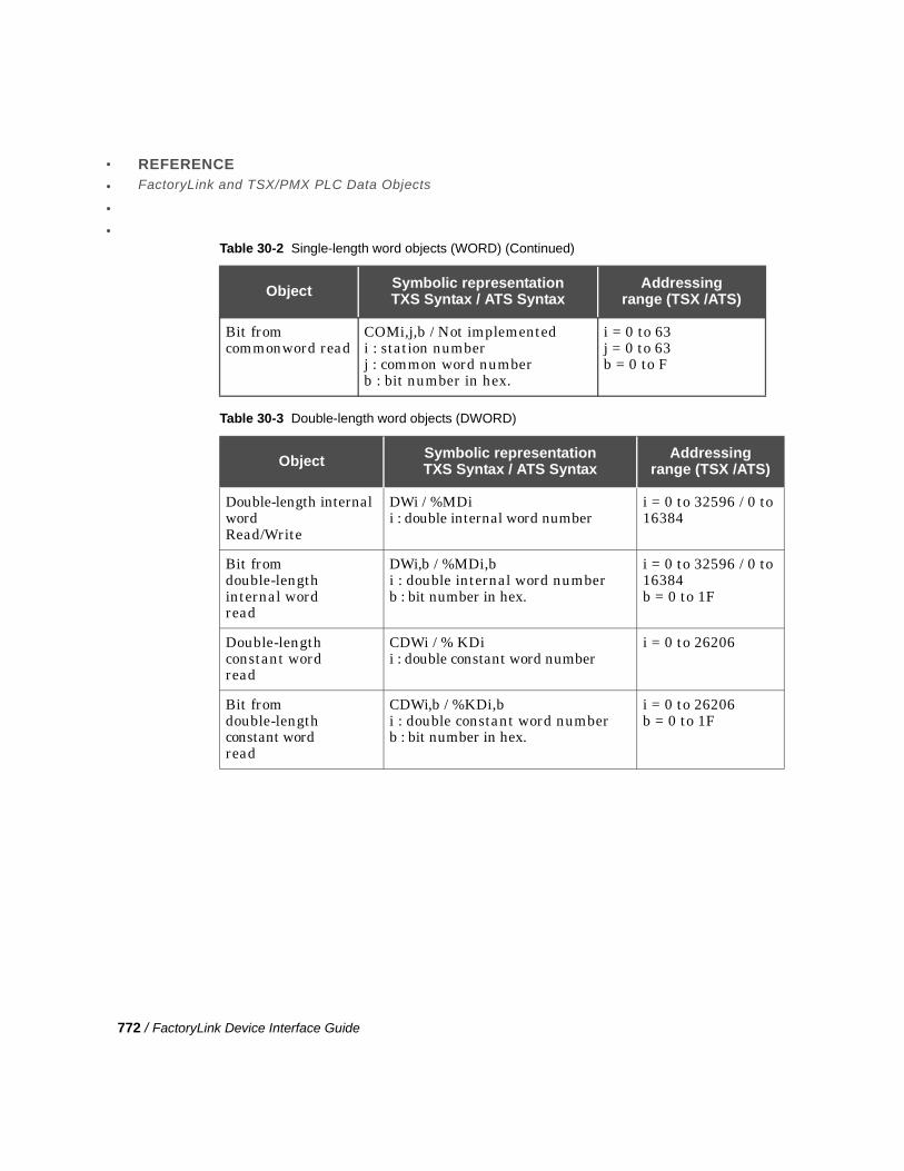
REFERENCEFactoryLink and TSX/PMX PLC Data Objects
772 / FactoryLink Device Interface Guide
••••
Bit from commonword read
COMi,j,b / Not implementedi : station numberj : common word numberb : bit number in hex.
i = 0 to 63j = 0 to 63b = 0 to F
Table 30-3 Double-length word objects (DWORD)
Object Symbolic representationTXS Syntax / ATS Syntax
Addressingrange (TSX /ATS)
Double-length internal wordRead/Write
DWi / %MDii : double internal word number
i = 0 to 32596 / 0 to 16384
Bit from double-length internal wordread
DWi,b / %MDi,bi : double internal word numberb : bit number in hex.
i = 0 to 32596 / 0 to 16384b = 0 to 1F
Double-length constant wordread
CDWi / % KDii : double constant word number
i = 0 to 26206
Bit from double-lengthconstant word read
CDWi,b / %KDi,bi : double constant word numberb : bit number in hex.
i = 0 to 26206b = 0 to 1F
Table 30-2 Single-length word objects (WORD) (Continued)
Object Symbolic representationTXS Syntax / ATS Syntax
Addressingrange (TSX /ATS)

REFERENCEFactoryLink and TSX/PMX PLC Data Objects
FactoryLink Device Interface Guide / 773
30
Telemecan
iqu
e
The floating point numbers are stored with IEEE single precision format (32 bits) inside the PLC and with IEEE double precision format (64 bits) inside FactoryLink. This may induce a lost of precision when exchanging data between the PLC and FactoryLink.
Table 30-4 Double-length floating point word objects: FDWORD
Object Symbolic representationTXS Syntax / ATS Syntax
Addressingrange (TSX /ATS)
Double-length floating point constant word read
FCDWi / %KFii: constant float word number
i = 0 to 32596 / 0 to 16384
Double-length floating point wordread/write
FCDWi,b / %MFi,bi : float internal word number
i = 0 to 32596 / 0 to16384
Table 30-5 I/O objects (I/O)
Object Symbolic representationTXS Syntax / ATS Syntax
Addressingrange (TSX /ATS)
Discrete I/O module input bitread
Ixy,b / Not implementedx : rack number in hex.y : module number in hex.b : bit number in hex.
x = 0 to Fy = 0 to 7b = 0 to F
Discrete I/O module output bitwrite
Oxy,b / Not implementedx : rack number in hex.y : module number in hex.b : bit number in hex.
x = 0 to Fy = 0 to 7b = 0 to F
Register bitread
IWxy,i / Not implementedx : rack number in hex.y : module number in hex.i : word number
x = 0 to Fy = 0 to 7i = 0 to 7

REFERENCEFactoryLink and TSX/PMX PLC Data Objects
774 / FactoryLink Device Interface Guide
••••
Bit from read register word read
IWxy,i,b / Not implementedx : rack number in hex.y : module number in hex.i : word numberb : bit number in hex.
x = 0 to Fy = 0 to 7i = 0 to 7b = 0 to F
Write register word OWxy,i / Not implementedx : rack number in hex.y : module number in hex.i : word number
x = 0 to Fy = 0 to 7i = 0 to 7
Bit assigned to Grafcet read
Xi / Not implementedi : step number
i = 0 to 511
Read Timer Ti,P/V/R/D / Not Implementedi : timer numberP : preset valueV : current valueR : timer runningD : timer done
i = 0 to 127
Timer Write preset word
Ti,P / Not implementedi : timer number
i = 0 to 127
Monostable Read Mi,P/V/R / Not implementedi : monostable valueP : preset valueV : current valueR : monostable running
i = 0 to 31
Monostable Write preset word
Mi,P / Not implementedi : monostable number
i = 0 to 31
Read Up/DownCounter
Ci,P/V/E/F / Not implementedi : counter numberP : preset valueV : current valueE : upcount overflowF : downcount overflow
i = 0 to 255
Table 30-5 I/O objects (I/O) (Continued)
Object Symbolic representationTXS Syntax / ATS Syntax
Addressingrange (TSX /ATS)

REFERENCEFactoryLink and TSX/PMX PLC Data Objects
FactoryLink Device Interface Guide / 775
30
Telemecan
iqu
e
Num Objects
FactoryLink allows access to a sub-group of NUM programmed in ladder objects. The list is:• Saved variables ( %Mi )• Non-saved variables ( %Vi )• Common words (%Si )
Up/Down Counter Write preset word
Ci,P / Not implementedi : counter number
i = 0 to 255
Read register Ri,I/O/E/F / Not implementedi : register numberI : input wordO : output wordE : empty registerF : full register
i = 0 to 127
Register Input wordwrite
Ri,I / Not implementedi : register number
i = 0 to 127
Table 30-5 I/O objects (I/O) (Continued)
Object Symbolic representationTXS Syntax / ATS Syntax
Addressingrange (TSX /ATS)

REFERENCEFactoryLink and TSX/PMX PLC Data Objects
776 / FactoryLink Device Interface Guide
••••
i = hexadecimal address of the objectj = Number of the bit in the word
* For this object, only addresses where the low byte is lower or equal to H7E are allowed.
Caution: For NUM two words are consecutive and disjoin if they are separated by 2 unities. And in the same way two long words have to be separated by 4 unities.
Table 30-6 Num Objects
Object
Symbolic representatio
n Num syntax
Addressing range
Saved VariablesWord Read/WriteDouble Word Read/WriteBit from Word Read
%Mi.W%Mi.L%Mi.j
i=< 77FEi=< 77FCi=< 77FE, j<8
Non-Saved VariablesWord Read/WriteDouble Word Read/WriteBit from Word Read
%Vi.W%Vi.L%Vi.j
i=< 77FEi=<= 77FCi=< 77FE, j<8
Common WordWord Read/Write %Si.W i=< 3F7E *

REFERENCEFactoryLink and TSX/PMX PLC Data Objects
FactoryLink Device Interface Guide / 777
30
Telemecan
iqu
e
As a result...
To take avantage of the algorithm which minimizes the number of requests, it’s recommended to write odd word series or even word series. For long word write series of long word equal modulo 4.
Examples :
Read table Tab0 = %M0.W,%M2.W,%M1A.W,W78.W generates 1 read request of 60 words.
Read table Tab1 = %M11.W,%M1B.W,%M1D.W,%M20.W,%M23.W,%M25.W generates 3 read requests. Reading of 7 words from %M11.W, Reding of the word %M20 and reading of 2 words from %M23.
Read table Tab2 = %V25.L,%V29.L,%V2D.L,%V2E.L,%V32.L,%V34.L,%V36.L generates 4 requests. Reading of 3 long words from %V25.L, Reading of 2 long words from %V2E.L , Reading of long word %V32.L and Reading of long word %V34.L.
Write table Tab3 = %S10.W,%S12.W,%S16.W,%S17.W generates3 write requests. Writing of 2 words from %S10.W, writing word %S16.W and writing word %S17.W.
Write table Tab4 = %M100.L,%M104.L,%M108.L,%M10A.L,%M10C.L,%M10D.L,%M111.L generates 4 write requests. Writing of 3 long words from %M100.L, writing of %M10A.L, writing of %M10C.L and writing of 2 long words from %M10D.L
For NUM only the bits from 0 to 7 are available and are coded with the high byte of the word.
Table 30-7
Wi high Byte Low Byte
Wi+1 high Byte Low Byte
Wi+2 High Byte Low Byte

REFERENCEUnsolicited Data Configuration Example
778 / FactoryLink Device Interface Guide
••••
UNSOLICITED DATA CONFIGURATION EXAMPLE
When FactoryLink receives unsolicited data from a PLC, it compares the UNI-TE address of the data received (a PLC and sender text block function) with the addresses of the logical stations assigned to the message type elements in the configuration tables. If a matching address is found, it automatically updates the element assigned to this address using the data of the request received.
A single Message type element must be assigned to a logical station; otherwise, only the first element encountered in the table with the lowest number will be updated.
On a UNI-TELWAY bus, Serial Port:• Master PLC:
Unsolicited data is generated by a master PLC from a text block. Configure the CPL type text block TXT, for OUTPUT with:TXTi,C = H’FC’TXTi,M = H’xx65’ where xx is the location of the TSX SCM module in the rack (FF for the built-in TSX SCI port)TXTi,L = Number of bytes to send.
• Slave PLC:
Table 30-8
Wi b7, b6, b5, b4, b3, b2, b1, b0 //////////////////////////////////
Wi+1 b7, b6, b5, b4, b3, b2, b1, b0

REFERENCEUnsolicited Data Configuration Example
FactoryLink Device Interface Guide / 779
30
Telemecan
iqu
e
To send unsolicited data from a UNI-TELWAY slave to a FactoryLink system, configure the CPL type text block for OUTPUT with:
The UNI-TELWAY module is located in slot 3.
In these examples, the lowest FactoryLink address (H’65’) corresponds to the address of Slave 1. If FactoryLink uses other slave addresses such as 10 to 25 (also referred to as data link addresses), the lowest address is H’6E’ (100+10 in decimal notation).
TXTi,M = H’TSX SCM slot, sender address + 64’
TXTi,C = H’07FC’ Category/Request code
TXTi,L = 6 + number of usable bytes
If the transmission buffer address = Wi
Wi = H’network number/00’
Wi + 1 = H’gate number/station number’
Wi + 2 = H’ (64 + lowest Monitor 77 address) FE’ E.g. H’65FE’
Wi + 3 = Data to send
Example:
Master station on multi-drop bus 0.
M77 addresses 1 to 15.
Slave station: ad0 = H ‘10’ (16),
ad1 = H ‘11’ (17),
ad2 = H ‘12’ (18).

REFERENCEUnsolicited Data Configuration Example
780 / FactoryLink Device Interface Guide
••••
Configure the following text block to send unsolicited data from a slave device to FactoryLink:
On a MAPWAY/FIPWAY/ETHWAY network:
Configure the TXT type NET function block for OUTPUT with to send unsolicited data from a network station to the FactoryLink system:
TXTi for OUTPUT
TXTi,M = H’0375’ (slot 3, sender address (H’64’ + ad1))
TXTi,C = H’07FC’ (unsolicited data request code)
TXTi,L = 6 + n (n = number of bytes to send)
Address of Buffer Wi :
Wi = H’0000’ (network number 0)
Wi + 1 = H’05FE’ (gate H’05’, station H’FE’)
Wi + 2 = H’65FE’ (Monitor 77 address H’64’ + 1)
Wi + 3 = data to send
TXTi,A = H’Monitor 77 network/station address’
TXTi,T = 0 Monitor 77 reception text block number (always 0)
TXTi,L = 2 + number of bytes to send
Wi = H’07FC’ unsolicited data category/request code
Wi + 1 = data to send

REFERENCEUnsolicited Data Configuration Example
FactoryLink Device Interface Guide / 781
30
Telemecan
iqu
e
In this example, the first station is configured to receive unsolicited data sent from slave 17.
The second station is configured to receive unsolicited data sent by text block 3 of the master PLC application.
The third station is configured to receive unsolicited data from text block 1 of a PLC application connected to the network as station 7.
Unsol1: FactoryLink real-time database element updated on reception of unsolicited data from slave 17.
Unsol2: FactoryLink real-time database element updated on reception of unsolicited data from master text block 3.
Unsol3: FactoryLink real-time database element updated on reception of unsolicited data from text block 1 of station number 7 on XWAY network 1.
Table 30-9 Logical Station Information Panel Entries
Network Number
Station Number
Gate Number
Module Number
Device Number
0 FE 5 FE 74
0 FE 5 FE 74
1 7 11 0 0
Table 30-10 Read/Write Information Panel Entries for Unsolicited Read
Logical Station Tag Name PL7 Object
1 Unsol1 TXT
2 Unsol2 TXT
3 Unsol3 TXT

REFERENCEUnsolicited Data Configuration Example
782 / FactoryLink Device Interface Guide
••••

FactoryLink Device Interface Guide / 783
• • • •
31
Telemecan
iqu
e
Chapter 31
Telemecanique Error Messages
This chapter describes the messages reporting operations and error conditions that can be generated and displayed for the Telemecanique protocol module.
Bad DCT file
Cause: The specified file is corrupt.
Action: Delete the files from the FLAPP\DCT directory and restart FactoryLink.
Cannot connect LPORT <lport number>
Cause: (UNI-TELWAY only) The master PLC does not poll the UNI-TELWAY slaves as expected.
Action: Ensure the UNI-TELWAY master PLC polls the range of communication slaves configured for the task.
Cannot find duntiw01.sys configuration in config.sys
Cause: TECOM has been invoked on UNI-TELWAY, and the associated UNI-TELWAY driver is not installed in the system.
Action: Install the UNI-TELWAY driver before invoking TECOM.
Cannot open driver <driver name>
Cause: The communication task cannot open the requested associated communication driver.
Action: Ensure the software driver is installed in the system.

TELEMECANIQUE ERROR MESSAGES
784 / FactoryLink Device Interface Guide
••••
Cannot read edi configuration
Cause: No external device definition is configured.
Action: Configure the EDI panel for the device.
Cannot read te__ configuration
Cause: No Telemecanique configuration is found.
Action: Configure the Telemecanique panels.
Cannot send request (no remote ack)
Cause: (ETHWAY only) An addressed PLC is not physically connected to the network.
Action: Ensure all addressed PLCs are physically connected to the ETHWAY network.
duntlw01.sys ‘NBR=’ parameter too small (mini = 2)
Cause: The UNI-TELWAY driver must be configured to respond for a minimum of two slaves.
Action: Modify the NBR field in the config.sys file.
Link is spurious
Cause: (UNI-TELWAY only) An unexpected, unsolicited message has been received.
Action: Ensure the PLC is sending unsolicited messages to the first UNI-TELWAY slave number reserved for this purpose.

TELEMECANIQUE ERROR MESSAGES
FactoryLink Device Interface Guide / 785
31
Telemecan
iqu
e
Link timeout from <LSTA xxx>
Cause: The response from logical station <xxx> was not received within the configured timeout period. The physical link may have been broken while requests were still waiting for a response.
Action: Increase the timeout value in the Telemecanique Logical Station configuration panel.
Logical port definition missing
Cause: The External Device Definition panel does not have a TE__/CUSTOM logical port configured.
Action: Configure the logical port on the External Device Definition panel.
Cause: The Telemecanique panel does not define a logical port on the invoked XWAY network.
Action: Define the logical port on the Telemecanique panel.
Cause: Definitions on the EDI and Telemecanique panels don’t match.
Action: Ensure the definitions match in both EDI and Telemecanique.
Lport slaves range is too small (mini=2)
Cause: The Telemecanique communication task must use a minimum of two slaves.
Action: Ensure the first and last slave fields have been configured properly.
Maximum table count reached for Block Read
Cause: More than 200 block read tables are configured.
Action: Ensure less than 200 block read tables are configured.
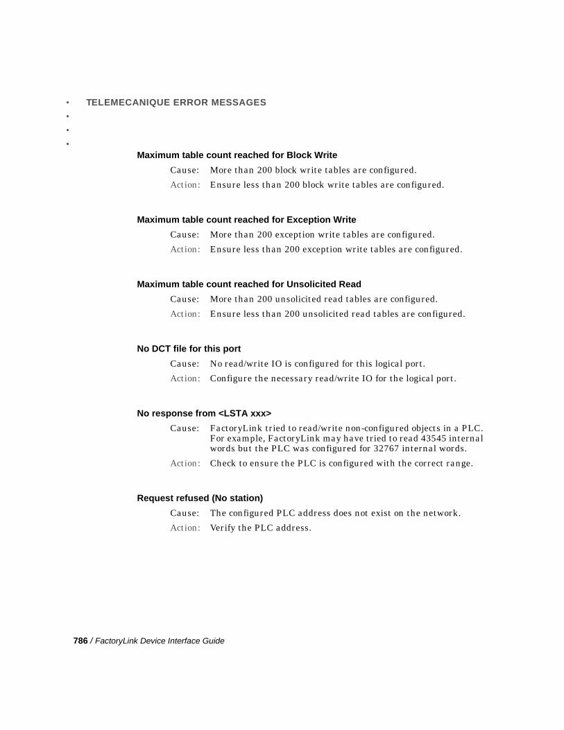
TELEMECANIQUE ERROR MESSAGES
786 / FactoryLink Device Interface Guide
••••
Maximum table count reached for Block Write
Cause: More than 200 block write tables are configured.
Action: Ensure less than 200 block write tables are configured.
Maximum table count reached for Exception Write
Cause: More than 200 exception write tables are configured.
Action: Ensure less than 200 exception write tables are configured.
Maximum table count reached for Unsolicited Read
Cause: More than 200 unsolicited read tables are configured.
Action: Ensure less than 200 unsolicited read tables are configured.
No DCT file for this port
Cause: No read/write IO is configured for this logical port.
Action: Configure the necessary read/write IO for the logical port.
No response from <LSTA xxx>
Cause: FactoryLink tried to read/write non-configured objects in a PLC. For example, FactoryLink may have tried to read 43545 internal words but the PLC was configured for 32767 internal words.
Action: Check to ensure the PLC is configured with the correct range.
Request refused (No station)
Cause: The configured PLC address does not exist on the network.
Action: Verify the PLC address.

TELEMECANIQUE ERROR MESSAGES
FactoryLink Device Interface Guide / 787
31
Telemecan
iqu
e
Run option not found
Cause: The Telemecanique communications driver option bit is not validated.
Action: Install the option bit.
Unsol. datagram received on unexcepted slave
Cause: An unsolicited message has been received on an unexcepted communication socket.
Action: Ensure the sender (PLC) addresses the message to a configured logical station.

TELEMECANIQUE ERROR MESSAGES
788 / FactoryLink Device Interface Guide
••••

• • • • • • • • • • • • • • • • • • • • • • • • • • • • • •
Part IPart IVRAPD Drivers
The Rapid Application Protocol Driver principle (RAPD) enables easy and rapid protocol-driver configurations for FactoryLink applications. RAPD is based on the Intertask Mail Exchange standard or IMX, which defines a way for a protocol driver task to communicate with the I/O Translator task. The RAPD system consists of a protocol driver which communicates with external devices (RTUs and PLCs) and the I/O Translator which controls data storage in the FactoryLink real-time database. This enables communications between the driver and a device to be very efficient. All data is referenced between the driver and the I/O Translator in terms of datasets. Datasets, described in the next section, define memory regions or locations of data within a device.
The manual for the I/O Translator task, AB RSLINX protocol driver, and the MBUSTCP protocol driver are included in this section. Other RAPD protocol driver manuals are included on the documentation CD. If you need more information about rapid drivers, refer to the I/O Translator Guide.


32
Extern
al Device
Interface
FactoryLink Device Interface Guide / 791
• • • •Chapter 32
External Device Interface for AB_RAPD
This chapter introduces you to the AB__RAPD (Allen Bradley_Rapid Application Protocol Driver) interface and tells you how to start the associated protocol module.
While this chapter provides information about all of the AB__RAPD protocol-specific data entry requirements, the I/O Translator Guide provides more information. This second manual give you the information necessary to define datasets and read/write triggers. It also explains how to use the I/O Translator task (IOX) to quickly and easily configure FactoryLink applications.
OVERVIEW
RAPD drivers depart from USDATA’s External Device Interface (EDI) technology. RAPD drivers are based on the Intertask Mail Exchange architecture. This architecture defines the task message handling between a protocol driver task and IOX.
The IOX task issues commands to the protocol driver to access an external device. The protocol driver, in turn, communicates to the external device(s). IOX might call on a driver to send data to, or to retrieve data from, an external device.
A driver, on the other hand, can send unsolicited data to the IOX. Any required conversions on the data going to and received from the protocol driver is handled by the IOX task.
The FactoryLink AB__RAPD task, the IOXLATOR task, and the Allen-Bradley RSLinx™ task provides a device interface with which a programmable logic controller (PLC) and a small logic controller (SLC) can communicate with FactoryLink, across one or more Allen-Bradley proprietary networks.
The AB__RAPD task can communicate with these Allen-Bradley devices:• PLC-2™• PLC-3™ • PLC-5™ • PLC-5/250 (Pyramid Integrator)

EXTERNAL DEVICE INTERFACE FOR AB_RAPDHow to Use This Chapter
792 / FactoryLink Device Interface Guide
••••
• PLC-5/xxE (Direct Ethernet link only)• SLC-500™ series 01, 02, 03, and 04 processors
Additionally, the tasks can run concurrently with software other than FactoryLink that is also using RSLinx.
AB__RAPD Data Highway Plus (DH+) communications are established through an Allen-Bradley KT, KTX, 1784-KT, 1784-KT2, or 1784-PCMK card port. The DH+ links with other networks, including another DH+, a Data Highway 485 (DH-485), or a Data Highway™ (DH) via a compatible Allen-Bradley network interface module.
AB__RAPD also communicates through an Ethernet™ port using the TCP/IP network protocol. Communications with Allen-Bradley devices occurs through either a PLC-5/250 with an Ethernet interface module providing a bridge to a DH+ network or through a direct Ethernet link to a device from the PLC-5/xxE family. Through the Pyramid Integrator, the AB__RAPD task communicates with stations on the local DH+ link and with stations on other networks, including DH-485, DH, and DH+.
AB__RAPD also communicates through a serial port with Allen-Bradley PLC-2, PLC-3, PLC-4, PLC-5 and PLC-250 devices.
HOW TO USE THIS CHAPTER
Use this chapter in conjunction with the I/O Translator Guide to configure the FactoryLink tags into datasets and read/write triggers. The IOXLATOR also handles the type conversion between the Allen-Bradley and FactoryLink data types.
In addition, the FactoryLink ECS Device Interface Guide section for the KTDTL and NetDTL interface can be referenced for Allen-Bradley data types and addresses.
Note
SLC-5/01, SLC-5/02, and SLC-5/03 processors require an interface module.SLC-5/04 processors connect directly to a Data Highway Plus™.

EXTERNAL DEVICE INTERFACE FOR AB_RAPDAB__RAPD at a Glance
FactoryLink Device Interface Guide / 793
32
Extern
al Device
Interface
AB__RAPD AT A GLANCE
This section provides a quick cross-reference to the IOXLATOR and indicates where to find specific information in this supplement.
I/O Translator DatasetDefinition
You create the dataset definitions by filling out the I/O Translator Dataset Definition panel of the IOXLATOR definition panels. This includes read/write triggers and completion and status tags.For descriptions of the specific entries you make in this panel, refer to this supplement. See “Configuring the I/O Translator Definition Panel” on page 798.
I/O Translator TagDefinition
For each dataset, define the tags that make up the dataset using the I/O Translator Tag Definition panel of the IOXLATOR definition panels.For descriptions of the specific entries you make in this panel, refer to this supplement. See “Configuring the I/O Translator Definition Panel” on page 798.
AB RSLinx Port Definition For each logical port, define a specific hardware interface (KT card, Ethernet) in the AB RSLinx Port Definition panel of the AB__RAPD definition panels.For descriptions of the specific entries you make in this panel, refer to this supplement. See“Configuring the AB RSLinx Port Definition Panel” on page 800.
AB RSLinx StationDefinition
For each logical port, define the Allen-Bradley devices connected to the port in the AB RSLinx Station Definition panel of the AB__RAPD definition panels.For descriptions of the specific entries you make in this panel, refer to this supplement. See “Configuring the AB RSLinx Station Definition Panel” on page 802.
AB RSLinx DatasetDefinition
For each station, list one or more datasets, previously defined in the IOXLATOR definition panels, and the address of the data in the station.For descriptions of the specific entries you make in this panel, refer to this supplement. See “Configuring the AB RSLinx Dataset Definition Panel” on page 807.

EXTERNAL DEVICE INTERFACE FOR AB_RAPDAB__RAPD at a Glance
794 / FactoryLink Device Interface Guide
••••
Technical Notes Lists the data type conversions to be used by the IOXLATOR for the various Allen-Bradley data types.Refer to “Technical Notes” on page 810 for additional notes specific to the EDI driver for use in setting up the AB__RAPD driver.
System Messages For information about messages unique to AB_RAPD, see “Run-Time Application Messages” on page 811.

EXTERNAL DEVICE INTERFACE FOR AB_RAPDAccessing the AB_RAPD Configuration Panels
FactoryLink Device Interface Guide / 795
32
Extern
al Device
Interface
ACCESSING THE AB_RAPD CONFIGURATION PANELS
When you choose AB RSLinx Driver from the Configuration Manager Main Menu, the AB__RAPD configuration panels are displayed.
Before completing the A
Before completing the AB__RAPD configuration panels, you must complete the I/O Translator Definition panels.

EXTERNAL DEVICE INTERFACE FOR AB_RAPDConfiguring the AB RSLinx Driver Mailbox Panel
796 / FactoryLink Device Interface Guide
••••
CONFIGURING THE AB RSLINX DRIVER MAILBOX PANEL
To bring the AB RSLinx Driver Mailbox panel to the foreground, click on its title bar in the display of all configuration panels.
Specify the mailbox of the AB RSLinx driver. The IOX communicates with the AB RSLinx driver by writing to this mailbox.
When the panel is complete, click on Enter to validate the information. Define the data type (mailbox) for any tag names displayed in the Tag Definition dialog.
AB RSLinx Driver MailboxTag
This mailbox belongs to the AB RSLinx driver task. Any task that wants to communicate with the AB RSLinx driver must write to this mailbox.Valid Entry: standard tag nameValid Data Type: mailbox
Description (Optional) Reference information about this mailbox tag.Valid Entry: alphanumeric string of up to 21
characters

EXTERNAL DEVICE INTERFACE FOR AB_RAPDConfiguring the AB RSLinx Driver Mailbox Panel
FactoryLink Device Interface Guide / 797
32
Extern
al Device
Interface
Table 32-1 provides sample entries for a row defining a AB RSLinx Driver Mailbox:
Table 32-1 Table 1 Sample AB RSLinx Driver Mailbox Panel Entries
Column
AB RSLinx Driver Mailbox Tag
DRVMBX The IOX communicates with the AB RSLinx driver by writing to this mailbox.
Description

EXTERNAL DEVICE INTERFACE FOR AB_RAPDConfiguring the I/O Translator Definition Panel
798 / FactoryLink Device Interface Guide
••••
CONFIGURING THE I/O TRANSLATOR DEFINITION PANEL
To bring the I/O Translator Definition panel to the foreground, click on its title bar in the display of all configuration panels or click on Next from the AB RSLinx Driver Mailbox panel.
Complete a row for each IOX with which the AB RSLinx driver communicates. The AB RSLinx driver communicates with the IOX by writing to this mailbox. The AB RSLinx driver communicates with multiple IOXs.
When the panel is complete, click on Enter to validate the information. Define the data type (mailbox) for any tag names displayed in the Tag Definition dialog.
I/O Translator Mailbox Tag This mailbox belongs to the IOX task. Any task that wants to communicate with the IOX must write to this mailbox. This must be the same tag defined in the IOX Mailbox Definition table.Valid Entry: standard tag nameValid Data Type: mailbox
Max MSG Maximum number of messages that can reside in the IOX’s mailbox.Valid Entry: 1 - 9999 (default = 100)
LAN Define whether the IOX communicates across a LAN. This field is currently not used. Valid Entry: no, yes (default = no)
Description (Optional) Reference information about this Mailbox tag.Valid Entry: alphanumeric string of up to 21
characters

EXTERNAL DEVICE INTERFACE FOR AB_RAPDConfiguring the I/O Translator Definition Panel
FactoryLink Device Interface Guide / 799
32
Extern
al Device
Interface
Table 32-2 provides sample entries for a row defining a I/O Translator.
Table 32-2 Sample I/O Translator Definition Panel Entries
Column Entry Description
I/O Translator Mailbox Tag
IOXMBX IOX mailbox tag.
Max MSG 100 Number of messages that can reside in the IOX’s mailbox.
LAN No Currently not used.
Description

EXTERNAL DEVICE INTERFACE FOR AB_RAPDConfiguring the AB RSLinx Port Definition Panel
800 / FactoryLink Device Interface Guide
••••
CONFIGURING THE AB RSLINX PORT DEFINITION PANEL
To bring the AB RSLinx Port Definition panel to the foreground, click on its title bar in the display of all configuration panels or click on Next from the I/O Translator Definition panel.
Complete a row for each port used by the driver in this application. A port can be a serial port, an Ethernet network connection, a KT, or KTC card.
Port Name Give this port a name. Define one port per line and do not include spaces in the name. You can define as many ports in this panel as are available on the system.Valid Entry: alphanumeric string of up to 16
characters
Response Timeout Enter the length of time (in tenths of seconds) the protocol module waits to receive a response to a read or write command.
For example, enter 30 for a time out of three seconds.Valid Entry: 0 - 200 (default = 20)
Interface Type Select the port type.Valid Entry: Serial
KT/KTXKTCNetDTL

EXTERNAL DEVICE INTERFACE FOR AB_RAPDConfiguring the AB RSLinx Port Definition Panel
FactoryLink Device Interface Guide / 801
32
Extern
al Device
Interface
When the panel is complete, click on Enter to validate the information. Define the data type (analog) for any tag names displayed in the Tag Definition dialog.
Table 32-3 provides sample entries for a row defining a port:
Interface Number The driver number as defined by RSLinx.
For example: AB_ETH-1 enter 1, AB_KT-2 enter 2.Valid Entry: 1 - 200 (default = 1)
Port Status Optional Analog tag to show port status. -1 indicates the port is not active. A positive value indicates the driver ID of the RSLinx driver active for that port.
Valid Entry: standard tag nameValid Data Type: analog
Table 32-3 Table 3 Sample AB RSLinx Port Definition Panel Entries
Column Entry Description
Port Name Port1 The name of this port is Port1.
Response Timeout
20 The timeout value is 2 seconds.
Interface Type KT/KTX This port is a KT card.
Interface Number
1 This is the port defined as AB_KT-1 by RSLinx.
Port Status port1_status Tag name of analog tag to hold the port status value.

EXTERNAL DEVICE INTERFACE FOR AB_RAPDConfiguring the AB RSLinx Station Definition Panel
802 / FactoryLink Device Interface Guide
••••
CONFIGURING THE AB RSLINX STATION DEFINITION PANEL
From the AB RSLinx Port Definition panel, select the row for the table you are configuring and click on Next to bring the AB RSLinx Station Definition panel to the foreground. This panel contains additional columns not shown.
Complete a row for each Allen-Bradley device connected to the port.
Station Name Give this station a name. Define one station per line and do not include spaces in the name. You can define as many stations in this panel as are available on this port.Valid Entry: alphanumeric string of up to 16
characters
Station Status Tag Optional name of a analog element to which any error code for this logical station is written.Valid Entry: standard tag nameValid Data Type: analog
Pyramid EI # (Decimal) Enter the number that corresponds to the station number specified with the TCP/IP address in the Allen-Bradley RSLinx configuration software.Valid Entry: 0 - 999 (default = 0)

EXTERNAL DEVICE INTERFACE FOR AB_RAPDConfiguring the AB RSLinx Station Definition Panel
FactoryLink Device Interface Guide / 803
32
Extern
al Device
Interface
Pyramid Channel ID(ASCII)
For applications that communicate with devices at addresses on the local network, enter the communications port in the appropriate Pyramid Integrator module to which this logical station is connected.Formats
0RM:[2,3] Resource Manager module, channel 2 or 3 (for example, 0RM:2)
[1-4]KA:[2,3] Card number, KA module, channel 2 or 3 (for example, 1KA:2)
If you are defining the Pyramid Integrator (PLC5/250) itself, leave this field blank.If you are defining a PLC-5/xxe connected directly to Ethernet, leave this field blank.For applications using off-link addressing, enter the location of the off-link station.Valid Entry: alphanumeric string of up to 22
characters
KT Card ID (ASCII) For applications that communicate with devices at addresses on the local network.
FormatKT:0 The module type followed by a colon,
and the channel number (for example, KT:0)
For applications using off-link addressing, enter the location of the off-link station.Valid Entry: alphanumeric string of up to 29
characters
Note
Do not use 1KT:0. The card number is defined using the interface number in the port definition table.

EXTERNAL DEVICE INTERFACE FOR AB_RAPDConfiguring the AB RSLinx Station Definition Panel
804 / FactoryLink Device Interface Guide
••••
Station Address (Octal) Enter the physical DH+, DH, or DH-485 address of the Allen-Bradley device.Address Limits
DH+ networks 0 - 77 (octal)DH networks 0 - 377 (octal)DH-485 networks 0 - 37 (octal)
Be sure to also complete the PYRAMID CHANNEL ID (ASCII) field associated with each device if the port is an Ethernet port.Valid Entry: 0 - 377 (Octal)
Station Type Enter the type of Allen-Bradley device from which data is read or to which data is written.Valid Entry:
PLC Same as PLC-2U.PLC-2 Same as PLC-2U.PLC-2P A-B PLC that is accessed by using the
A-B basic (PLC-2) unprotected-read and protected-write commands.
PLC-2U A-B PLC that is accessed by using the A-B basic (PLC-2) unprotected-read and unprotected-write commands.
PLC-3 A-B PLC-3; same as PLC3-KA.PLC-3KA A-B PLC-3 that is not a PLC-3SR.PLC-3SR A-B PLC-3 that uses a 1775-S5 or
1775-SR5 scanner for DH+ communications. This scanner allows faster bit write operations.
PLC-4 Same as PLC-2U.PLC-5 A-B PLC-5 new or old generation.PLC-250 A-B PLC5/250 Pyramid Integrator.SLC-500 SLC 500 series processor.

EXTERNAL DEVICE INTERFACE FOR AB_RAPDConfiguring the AB RSLinx Station Definition Panel
FactoryLink Device Interface Guide / 805
32
Extern
al Device
Interface
When the panel is complete, click on Enter to validate the information. Define the data type (digital) for any tag names displayed in the Tag Definition dialog.
Table 32-4 provides sample AB RSLinx Station Definition panel entries for AB RSLinx Port Definition table entries, which are defined in the table on page 801.
Tip
To enter a station type, go back to the field and press Ctrl+K. From the list of valid entries that appear, double-click the station type or highlight your choice and press Enter.
Encode Register Define the PLC register to use for an encoded exception write. Currently not used.Valid Entry: 1 - 9999
Read Disable Digital tag to enable or disable the read function for the device. Function is enabled if no tag is specified or the tag value is OFF. Function is disabled if the tag value is ON.Valid Entry: standard tag nameValid Data Type: digital
Write Disable Digital tag to enable or disable the write function for the device. Function is enabled if no tag is specified or the tag value is OFF. Function is disabled if the tag value is ON.Valid Entry: standard tag nameValid Data Type: digital
Receive Disable Digital tag to enable or disable the unsolicited receive function for the device. Function is enabled if no tag is specified or the tag value is OFF. Function is disabled if the tag value is ON.Valid Entry: standard tag nameValid Data Type: digital

EXTERNAL DEVICE INTERFACE FOR AB_RAPDConfiguring the AB RSLinx Station Definition Panel
806 / FactoryLink Device Interface Guide
••••
Table 32-4 Table 4 Sample AB RSLinx Station Definition Panel Entries
Column Entry Description
Port Name Port1 The table name defined in the AB RSLinx Port Definition panel is displayed.
Station Name Station1 The name of this station is Station1.
Station Status Tag
station1_status Tag name of analog tag to hold the port status value.
Pyramid EI # (Decimal)
No entry for this port type (KT).
Pyramid Channel ID (ASCII)
No entry for this port type (KT).
KT Card ID (ASCII)
KT:0 The module type and the channel number.
Station Address (Octal)
10 Address of the KT card.
Station Type PLC-5 PLC Type connected to the KT card.
Encode Register No entry.
Read Disable sta1_rd_disabl Digital tag to enable or disable the read function for this device.
Write Disable sta1_wr_disabl Digital tag to enable or disable the write function for this device.
Receive Disable sta1_rcv_disabl Digital tag to enable or disable the unsolicited receive function for this device.

EXTERNAL DEVICE INTERFACE FOR AB_RAPDConfiguring the AB RSLinx Dataset Definition Panel
FactoryLink Device Interface Guide / 807
32
Extern
al Device
Interface
CONFIGURING THE AB RSLINX DATASET DEFINITION PANEL
From the AB RSLinx Device Definition panel, select the row for the table you are configuring and click on Next to bring the AB RSLinx Dataset Definition panel to the foreground. This panel contains additional columns not shown.
This table links datasets to the physical PLC addresses. Complete a row for each dataset associated with the device.
I/O Translator Mailbox Tag IOX mailbox associated with this dataset.Valid Entry: standard tag nameValid Data Type: mailbox
Data Set Dataset control tag (digital) which is associated with the dataset specified by the IOX task.Valid Entry: standard tag nameValid Data Type: digital
Address Enter the address of the memory location being read or written. Valid Entry: alphanumeric string of up to 22
characters

EXTERNAL DEVICE INTERFACE FOR AB_RAPDConfiguring the AB RSLinx Dataset Definition Panel
808 / FactoryLink Device Interface Guide
••••
When the panel is complete, click on Enter to validate the information. Define the data type (digital) for any tag names displayed in the Tag Definition dialog.
Table 32-5 provides sample AB RSLinx Dataset Definition panel entries for AB RSLinx Port Definition table entries which are defined in the table on page 801.
Note
For more information about defining memory addresses for Allen-Bradley devices, refer to the Allen-Bradley addressing reference documentation for the appropriate device.
Len Number of elements to read.Valid Entry: 1 - 9999 (default = 1)
UR Determines whether to accept unsolicited messages for this dataset.Valid Entry: Y, N
Read Completion This trigger is set when the dataset is read from the external device.Valid Entry: standard tag nameValid Data Type: digital
Write Completion This trigger is set when the dataset is written to the external device.Valid Entry: standard tag nameValid Data Type: digital
Rcv Completion This trigger is set when the dataset is received from the external device with the unsolicited receive function.Valid Entry: standard tag nameValid Data Type: digital

EXTERNAL DEVICE INTERFACE FOR AB_RAPDConfiguring the AB RSLinx Dataset Definition Panel
FactoryLink Device Interface Guide / 809
32
Extern
al Device
Interface
Table 32-5 Table 5 Sample AB RSLinx Dataset Definition Panel Entries
Column Entry Description
Station Name Station1 The table name defined in the Station Definition panel is displayed.
I/O Translator Mailbox Tag
IOXMBX Tag name of the I/O Translator for this dataset.
Data Set analog_ds[0] Tag name of the digital tag identifying this dataset.
Address N:0 Defines integer register 0 as the starting address.
Len 16 Read 16 data elements.
UR N No unsolicited messages accepted for this dataset.
Read Completion ana0_rd_compl Tag name of the digital tag which receives the read completion trigger.
Write Completion ana0_wr_compl Tag name of the digital tag which receives the write completion trigger.
Rcv Completion Blank since no unsolicited messages are allowed.

EXTERNAL DEVICE INTERFACE FOR AB_RAPDTechnical Notes
810 / FactoryLink Device Interface Guide
••••
TECHNICAL NOTES
The entries shown in Table 32-6 must be made in the CONV field of the I/O Translator Tag Definition panel.
The following command line arguments are used in the System Configuration panel:
Table 32-6 Entries in the CONV Field
AB Data Type CONV
WORD WORD
PLC3_LONG LONG
LONG RLNG
3BCD BCD
4BCD BCD
PLC3_FLT IEEE
SLC_FLT IEEE
SLC_FLT IEEE
FLT RFLT
BIT BIT
-d Displays debug information on the screen.
-l Writes debug information to <FLAPP>\ab__rapd.log.

EXTERNAL DEVICE INTERFACE FOR AB_RAPDRun-Time Application Messages
FactoryLink Device Interface Guide / 811
32
Extern
al Device
Interface
RUN-TIME APPLICATION MESSAGES
During run time, FactoryLink generates and displays messages for the AB__RAPD protocol module on the Run-Time Manager screen. These messages are stored in FactoryLink database elements. You define the tag names for these elements in the AB RSLinx Station Definition table. See “Configuring the AB RSLinx Driver Mailbox Panel” on page Configuring the AB RSLinx Driver Mailbox Panel for information about configuring a message tag. See “Configuring the I/O Translator Definition Panel” on page 798 for information about configuring an analog tag.
Error Messages
The following messages might be displayed at startup.
NOCT
Cause: There is no AB__RAPD CT file.
Action: Check CTLIST for the correct AB__RAPD entry.
NOCTRECS
Cause: There are records missing in the AB__RAPD CT file.
Action: Check CTLIST for the correct AB__RAPD entry.
NOCTCLOSE
Cause: There is no AB__RAPD CT file.
Action: Check CTLIST for the correct AB__RAPD entry.
Port Type/Device Address mismatch PPP:SSS (PPP - Port Name, SSS - Station Name)
Cause: There is a problem with the station data for the given port.
Action: Check the configuration table entries for the station.
ADDRESS ERROR PPP:SSS:DDD (PPP - Port Name, SSS - Station Name, DDD - Dataset Name)
Cause: There is a problem with the dataset data for the given port.
Action: Check the configuration table entries for the dataset.

EXTERNAL DEVICE INTERFACE FOR AB_RAPDRun-Time Application Messages
812 / FactoryLink Device Interface Guide
••••
DTL_INIT (‘ErrNo’) - ‘ErrStr’
Cause: There is a problem initializing RSLinx.
Action: Check the error string in the RSLinx documentation.
ABSTOP
Cause: There is a problem initializing the IOXLATOR.
Action: Verify the IOXLATOR is running.
ABSTOP1
Cause: There is a problem registering the datasets with the IOXLATOR.
Action: Verify the datasets defined by AB__RAPD are defined by the IOXLATOR.
Internal: (connect) DTL_DRIVER_LIST ‘ErrStr’
Cause: There is a problem connection to a RSLinx driver.
Action: Check the error string in the RSLinx documentation.
DEFINE ERROR PPP:SSS:DDD(PPP - Port Name, SSS - Station Name, DDD - Dataset Name)
Cause: There is an incompatibility with the address or length of the dataset with the station type.
Action: Check the dataset parameters.
ABDTL unsol register error ‘ErrStr’
Cause: There is a problem registering to receive unsoliciteds from RSLinx.
Action: Check the error string in the RSLinx documentation.

EXTERNAL DEVICE INTERFACE FOR AB_RAPDError Codes
FactoryLink Device Interface Guide / 813
32
Extern
al Device
Interface
ERROR CODES
The following errors are returned to the IOXLATOR at run time.
Table 32-7 IOXLATOR Errors
Error Code Description
3 - 82 Cause: Error codes returned from RSLinx. Error text may be displayed on AB__RAPD screen. Error text may also be found in the RSLinx documentation
Action: Depends on the specific error code.
1001 Cause: The start address or length of a dataset being passed to AB__RAPD by the IOXLATOR is invalid.
Action: Check the IOXLATOR configuration table entries.
1002 Cause: The station read disable tag is set for the dataset being triggered for a read by the IOXLATOR.
Action: Reset the disable tag.
1003 Cause: The station write disable tag is set for the dataset being triggered for a write by the IOXLATOR.
Action: Reset the disable tag.
-1000 Cause: A bad unsolicited command was received.
Action: Locate the PLC sending the invalid command and reprogram it.
-1001 Cause: A bad unsolicited device code was received.
Action: Locate the PLC sending the invalid device code and reprogram it.
-1002 Cause: A bad PLC5 address was received in an unsolicited message.
Action: Locate the PLC sending the bad address and reprogram it.
-1003 Cause: A bad PLC3 address was received in an unsolicited message.
Action: Locate the PLC sending the bad address and reprogram it.

EXTERNAL DEVICE INTERFACE FOR AB_RAPDError Codes
814 / FactoryLink Device Interface Guide
••••

33
Extern
al Device
Interface
FactoryLink Device Interface Guide / 815
• • • •Chapter 33
MODBUS Ethernet Driver
PURPOSE
This chapter provides information about a collection of software tools used in conjunction with Modicon’s Quantum line of Programmable Logic Controllers (PLCs) and network operating equipment (NOE) ethernet modules.
This chapter is prepared to present the technical information programmers of these systems need to complete their applications.
The following guidelines help focus our purpose and goals to meet customer requirements:• Accuracy is paramount—This FactoryLink documentation must provide accurate and
reliable information and procedures.• Time is valuable—This FactoryLink documentation must guide the programmer through
what he needs to know quickly and efficiently.
AUDIENCE
The major audience of this chapter is the individual familiar with both the FactoryLink software and the Modicon’s Quantum line of PLCs.
In addition, FactoryLink Customer Support Services personnel use the procedures and examples included here to help you develop and troubleshoot your applications.
STRUCTURE OF THE MODBUS ETHERNET DRIVER SOFTWARE GUIDE
Use this chapter in this book along with the rest of the FactoryLink Documentation Set. Refer to the Preface in Fundamentals for the structure of the entire Documentation Set.
This chapter is divided into four sections:• Overview

MODBUS ETHERNET DRIVERHOW TO USE THIS GUIDE
816 / FactoryLink Device Interface Guide
••••
• I/O Translator and Protocol Driver Communications
• Panels
• Error Codes and Messages
HOW TO USE THIS GUIDE
The material in this chapter is presented sequentially in learning, then performance order. We recommend you read the entire chapter to familiarize yourself with the complete procedure before you proceed to develop your application.
. . . at a Glance
Included in this chapter is a section named . . . at a Glance. This section provides a quick key to locations for information to perform the procedures detailed in each section with hypertext links to those locations.
CONVENTIONS
The material in the Documentation Set adheres to the guidelines published in The Digital Technical Documentation Handbook by Schultz, Darrow, Kavanagh, and Morse; Developing International User Information by Jones, Kennelly, Mueller, Sweezy, Thomas, and Velez; and corporate style guidelines.
This chapter uses the following conventions:
Documentation Conventions
Table 33-1 Documentation Conventions
Convention Description
… Horizontal ellipsis points indicate the omission of material from an example. The information is omitted because it is not important to the topic being discussed.
.
.
.
Vertical ellipsis points indicate the omission of information from an example or command format. The information is omitted because it is not important to the topic being discussed.

MODBUS ETHERNET DRIVERHOW TO USE THIS GUIDE
FactoryLink Device Interface Guide / 817
33
Extern
al Device
Interface
italic type Italic type is used to denote user-supplied variables in command examples. Italic type also sets off references to specific documents.
monospace type Monospace type is used to denote command names and code examples or example output.
bold monospace type
Bold monospace type is used in command examples to indicate words that must be typed literally.
sans serif type Sans Serif type is used to set off field names, button names, and keys on the keyboard.
press nnnnn Press is used to denote a key on the keyboard. The key name will display in a sans serif type.
click on nnnnn Click on is used to denote a button on the screen. The button name will display in a sans serif type.
Shift+F1 The + indicates the keys must be pressed simultaneously.Shift+F1 indicates you hold down the Shift key while you press another key or mouse button (indicated here by F1).
Other key combinations are presented in the same manner.
F1 F2 F3 The space between the key callouts indicates press and release.The key sequence F1 F2 F3 indicates you press and release F1, then F2, and then F3.
Other key combinations are presented in the same manner
File>Open The > indicates a progression through a menu sequence.
File>Open indicates you choose Open from the File menu to perform the required action.
Other menu sequences are presented in the same manner.
Table 33-1 Documentation Conventions (Continued)
Convention Description

MODBUS ETHERNET DRIVERHOW TO USE THIS GUIDE
818 / FactoryLink Device Interface Guide
••••
Command Syntax
Example Syntax
command input_file [input_file…] {a|b} output_file
wherecommand is typed as it is displayed in the syntax.
input_file indicates a variable the user supplies.[input_file…] indicates the user can optionally supply multiple input file names, each name separated by a space.{a|b} indicates either the a or b must be specified as an argument.output_file indicates the user must specify an output file.
FLAPP\user\drw\mydrw.g The \ indicates the directory structure for the listed file.FLAPP\user\drw\mydrw.g indicates the drawing file mydrw.g is located in the drw sub-directory of the user sub-directory to the FLAPP directory.
Other directory structures are presented in the same manner.
Table 33-2 Command Syntax Conventions
[ ] Brackets indicate an optional argument. You can choose none, one, or all of the options.
{ } and | Braces indicate a choice. You must choose one of the elements. The vertical bar separates choices within braces.
… Ellipsis indicate repetition of the preceding item.
Table 33-1 Documentation Conventions (Continued)
Convention Description

MODBUS ETHERNET DRIVERHOW TO USE THIS GUIDE
FactoryLink Device Interface Guide / 819
33
Extern
al Device
Interface
Contact your Sales or Customer Support Representative for help with troubleshooting problems.
Also, help files are included for each configuration panel. Click on Help on the panel menu bar to access these files.

MODBUS ETHERNET DRIVERModbus ethernet driver at a glance
820 / FactoryLink Device Interface Guide
••••
MODBUS ETHERNET DRIVER AT A GLANCE
Table 33-3 Using the Modbus Ethernet Driver Software
For details on performing these steps... Go to...
1 Read about installing the Modbus Ethernet Driver software.
“Overview” on page 821
2 Read about I/O Translator and Protocol Driver communications, including datasets, read and block write, unsolicited receive, exception write, encoded write, and domain selection.
“I/O Translator and Protocol Driver Communications” on page 823
3 Read about configuring panels, including the Mailbox panel, the IOX Definition panel, the Device Definition panel, and the Dataset Definition panel.
“Configuring Panels” on page 826
4 Read about error codes and error messages.
“Error Codes and Messages” on page 838

MODBUS ETHERNET DRIVEROverview
FactoryLink Device Interface Guide / 821
33
Extern
al Device
Interface
OVERVIEW
The FactoryLink ECS Modbus Ethernet driver is used in conjunction with Modicon’s Quantum line of PLCs and network operating equipment (NOE) ethernet modules. The software enables data exchange between a Quantum PLC and a FactoryLink application on a 10 BaseT TCP/IP network.This driver software,
This section includes information on how to install Modbus Ethernet Driver Software.
INSTALLATION OF THE FACTORYLINK SOFTWARE
Install the FactoryLink ECS software if you have not already done so. If FactoryLink is already installed but the driver is not, refer to the Installation Guide for details to complete a supplemental installation. All necessary files, such as .AC, .CTG, .TXT and .KEY files associated with the driver, will be correctly installed.
The Modbus Ethernet task must be entered in the FactoryLink Configuration Manager (FLCM) System Configuration table. A new entry can be made with the following data if one does not already exist. If the task is added to the end of the list of tasks, increment the task index value by 1 + index value of the last task entry. Enter the following information exactly as shown.
This completes the installation of the driver.
Table 33-4 Modbus Ethernet Task
Task Name Description Executable File
MBUSTCP Modbus Ethernet Protocol Driver bin/mbustcp.exe

MODBUS ETHERNET DRIVERInstallation of the FactoryLink Software
822 / FactoryLink Device Interface Guide
••••
CAUTION
The Modbus ethernet driver is intended to be used over a 10 BaseT network.
Configure the Quantum network of PLCs according to Modicon’s recomme-
dations. Configure your system appropriately and troubleshoot any connec-
tions to the Quantum devices before running your FactoryLink application.
For example, if you are using Win/NT, you must set up the correct network
configuration to support 10 BaseT communications. Ping the Quantum
PLC(s) using the correct IP address to see if the device is visible on the net-
work. Modicon provides an ethernet diagnostic program to troubleshoot your
PC connection to the NOE ethernet module. This diagnostic program
is available from Modicon.

MODBUS ETHERNET DRIVERI/O Translator and Protocol Driver Communications
FactoryLink Device Interface Guide / 823
33
Extern
al Device
Interface
I/O TRANSLATOR AND PROTOCOL DRIVER COMMUNICATIONS
The Rapid Application Protocol Driver (RAPD) is based on a two-task system. The tasks are the driver, in this case, the Modbus Ethernet Driver (MBUSTCP) task, and the I/O Translator (IOX) task.
The driver task communicates directly with the PLC devices and, therefore, understands the required communications protocol. The IOX, on the other hand, requests the protocol driver to send/get data from the device(s). The IOX provides necessary data conversions for the protocol driver and handles the FactoryLink tag data storage. The two tasks communicate with one another via datasets and mailbox tags.
DATASETS
A dataset is a contiguous area of data (registers, memory locations) in an external device, such as a PLC. The protocol driver is responsible for defining the complete dataset area. The dataset area is the area in the device the driver accesses. Access may be Read or Write, depending on access restrictions the device manufacturer set.
Datasets are always assumed to be contiguous. The protocol driver must provide a start and length value to delimit the start and end values of the contiguous area. The contiguous area is also associated with a data type. The data type refers to the element type of the area in the device.
BLOCK READ AND WRITE
The block read and write commands are performed on a contiguous block of data in the PLC specified by the dataset. Both commands are initiated by the IOX. The IOX sends requests to the Modbus Ethernet protocol driver for reading or writing an entire dataset. Refer to the I/O Translator guide for details on configuring the IOX.
UNSOLICITED RECEIVE
The external device sends protocol messages to the FactoryLink workstation for an unsolicited receive. This means the action is initiated in the external device. The protocol driver checks if the received data is defined in one of its locally defined datasets. If it is, the data received from the external device is sent with the corresponding dataset information to the IOX. The IOX provides any necessary data conversion. The message is discarded if the message received from

MODBUS ETHERNET DRIVERI/O Translator and Protocol Driver Communications
824 / FactoryLink Device Interface Guide
••••
the external device has no matching dataset (the protocol driver never expected the message).
Events, such as alarms, are usually unsolicited. Some extra programming effort has to be done in the external device (ladder logic is required in a PLC) because the external device originates the messages.
EXCEPTION WRITE
An exception write is initiated by the FactoryLink workstation and writes data to the external device. Exception writes are write requests for an element within a dataset that has changed in value. Since only an element is written, the entire dataset is not written as a block. The protocol driver receives a request for exception write from the IOX. The first action the driver takes is to check if the write can be accomplished with one write message.
If the exception data element size is smaller than the size of the external device data type element, the data must be read first, patched with exception data, and written back. An example is a bit that must be written to in a word area. If this is not done, some data bits within the word may be overwritten in the external device. The data type of the dataset determines if this event occurs.
For example, if a left byte (BL) in a Holding Register (HREG) has to be written, then the specific data word must first be read because the size of a Holding Register is a word (16 bits). The BL has to be patched into the word just read and then written back to the external device.
The reading of data before writing slows down performance since message traffic is increased. Some devices provide a function to accomplish the write in the message. If your device does not have this feature, the encoded write is an alternative option.
ENCODED WRITE
The encoded write function is almost similar to the exception write in that both functions write single data elements. The difference is the exception write is an actual direct (block) write of data to register addresses whereas the encoded write achieves this end result indirectly. The encoded write is a block write of some register values to a external device. The data is written to registers that are part of some internal program, such as ladder logic. The ladder logic may be some programmed logic that manipulates specifies bits within a specified word. The information comes down in a block write message for the ladder logic to know what bits to change within a word.

MODBUS ETHERNET DRIVERI/O Translator and Protocol Driver Communications
FactoryLink Device Interface Guide / 825
33
Extern
al Device
Interface
One advantage of this method is for every element to be written, only one Modbus Ethernet write command is needed because the external device program does the actual operation on the data element (no reading before writing). A second advantage is the external device program can control all encoded writes because they are all written to one location in the external device.
The encoded write is defined by specifying a starting holding register address in the Encode Address field of the Modbus Ethernet Device Definition panel.
FACTORYLINK DOMAIN SELECTION
The standard domain for the Modbus Ethernet protocol driver is the SHARED domain, but it can also be used in the USER domain. The protocol driver communicates with a dedicated piece of hardware; therefore, only one task should be able to access the hardware. The task should be started by the SHARED Run-Time Manager if only one program accesses the hardware.
Note
The encoded write function is an optional feature the application may or may not use. This driver does not currently use this feature.
Note
The protocol driver and the IOX must be in the same domain (SHARED).

MODBUS ETHERNET DRIVERConfiguring Panels
826 / FactoryLink Device Interface Guide
••••
CONFIGURING PANELS
This section contains instructions for configuring the panels for the Modbus Ethernet Driver. These panels include:• Modbus Ethernet Mailbox panel• I/O Translator Definition panel• Modbus Ethernet Device Definition panel• Modbus Ethernet Dataset Definition panel
You access these panels by opening the Configuration Manager and selecting Modbus Ethernet Protocol Driver. Four panels are displayed with the titles of all visible for direct access. To access a specific panel, either• Position the cursor on a visible area of that panel and click the left mouse
button• Click on the Next/Previous buttons of the panel in full view
MAILBOX PANEL
The Modbus Ethernet Mailbox panel allows the user to define and initialize one mailbox tag for the Modbus Ethernet protocol driver for full operation of MCI.
The Modbus TCP/IP Driver Mailbox Definition screen goes here
Perform the following steps to define the fields on this panel:
1 Open the Configuration Manager Main Menu > Modbus Ethernet Protocol Driver.
2 Click on any visible part of the Modbus Ethernet Mailbox panel.
3 Complete the fields by entering the following information:
ProtocolDriver
MailboxTag
Tag name of the Modbus Ethernet protocol mailbox element that the application developer defines, to be referenced by an IOX task. The IOX task uses this mailbox to send requests to the Modbus Ethernet protocol driver.
Description: Description of the mailbox tag you enter.
Valid Entry standard element tag name
Valid Data Type mailbox

MODBUS ETHERNET DRIVERConfiguring Panels
FactoryLink Device Interface Guide / 827
33
Extern
al Device
Interface
DEFINITION PANEL
The Ioxlator Mailbox Definition panel allows the user to specify the IOX task. Only one mailbox tag is needed.
The Ioxlator Mailbox Definition screen shot goes here.
Perform the following steps to define the fields on this panel:
1 With the Configuration Manager>I/O Translator open, click on any visible part of the Modbus Ethernet IOX Definition panel.
2 Complete the fields by entering the following information:
IoxlatorMailbox
Tag
Tag name of an IOX mailbox element the Modbus Ethernet protocol driver task references. The IOX task uses this mailbox to receive data from the Modbus Ethernet protocol driver. This entry is required.
Max MSG Maximum number of requests for the protocol driver that can be queued in the mailbox tag. We recommend a value of 100 messages. The number of messages is limited by the size of an integer value (9999) and/or by the amount of available memory. The memory needed for a request depends on the size of the configured datasets. This entry is required.
Description: Description of the IOX mailbox element you define.
Valid Entry standard element tag name
Valid Data Type mailbox
Valid Entry 1 - 9999 (Default = 100)
Valid Data Type output only

MODBUS ETHERNET DRIVERConfiguring Panels
828 / FactoryLink Device Interface Guide
••••
DRIVER DEVICE DEFINITION PANEL
The Modbus Ethernet Device Definition panel allows the user to specify the logical devices for the communication.
The Modbus TCP/IP Driver Device Definition screen goes here.
Perform the following steps to define fields on this panel:
1 With the Configuration Manager>I/O Translator open, click on any visible part of the Modbus Ethernet Device Definition panel.
2 Complete the fields by entering the following information:
DeviceName
Logical user-assigned name assigned by the user to represent a particular communication device (Quantum01).
IPNetworkAddress
Network IP address of the PLC.
Status Tag Analog tag set by the Modbus Ethernet protocol driver task to indicate the overall status of communications to the device Any task can reference this tag to handle communication error situations.
Connec-tion
Timeout(secs)
Connection timeout defines the duration to wait for connection to the PLC. The default is 3 seconds. If you are experiencing problems connecting to a PLC, increase the timeout value.
ResponseTimeout
(secs)
Response timeout defines the duration to wait for response data to arrive (in seconds). The default is 3 seconds. If you are experiencing longer latency times for responses from a PLC, increase the timeout value.
Valid Entry alphanumeric string of up to 16 characters
Valid Entry standard element tag name
Valid Data Type analog

MODBUS ETHERNET DRIVERConfiguring Panels
FactoryLink Device Interface Guide / 829
33
Extern
al Device
Interface
ReadDisable
Real-time digital database element used to enable/disable read commands for the device. Read commands are enabled if no tag is defined or the status of the tag is OFF. Read commands are disabled if the status of the tag is ON.
WriteDisable
Real-time database element used to enable/disable write commands for the
device. Write commands are enabled if no tag is defined or the status of the
tag is OFF. Write commands are disabled if the status of the tag is ON.
Unsolicited Disable
Real-time database element used to enable/disable unsolicited commands
for the device. Unsolicited commands are enabled if no tag is defined or the
status of the tag is OFF. Unsolicited commands are disabled if the status of
the tag is ON.
Valid Entry standard element tag name
Valid Data Type digital
Valid Entry standard element tag name
Valid Data Type digital
Valid Entry standard element tag name
Valid Data Type digital

MODBUS ETHERNET DRIVERConfiguring Panels
830 / FactoryLink Device Interface Guide
••••
DATASET DEFINITION PANEL
The Modbus Ethernet Dataset Definition panel allows the user to specify datasets for a particular logical device and select different logical device names.
The Modbus TCP/IP Dataset Definition screen goes here.
Perform the following steps to define the fields on this panel:
1 With the Configuration Manager>I/O Translator open, click on any visible part of the Modbus Ethernet Dataset Definition panel.
2 Complete the fields by entering the following information:
IOXMailbox
Tag
Tag name of an IOX mailbox element the Modbus Ethernet protocol driver task references. The IOX task uses this mailbox to receive data from the Modbus Ethernet protocol driver. This entry is required.
Data Set Tag name representing a unique logical name for a data set. The name of the logical device is displayed in the Device Name field.
Type Type definition of the data type in the logical device (PLC). The data types
can be of type Coil, Digital Input, Input Registers, Holding Registers,
Extended Memory, and Statistics.
Place the cursor in the Type field and press Ctrl>K to access the entries for
this field. The table on the next page lists the data types you can enter into
this field.
Valid Entry standard element tag name
Valid Data Type mailbox
Valid Entry standard element tag name
Valid Data Type digital

MODBUS ETHERNET DRIVERConfiguring Panels
FactoryLink Device Interface Guide / 831
33
Extern
al Device
Interface
Table 33-5 Data Type Entries
Valid Entry Data Type Reference I/O Allowed
C Digital Output 0x reference READ/WRITE
CO Digital Output 0x reference READ/WRITE
COI Digital Output 0x reference READ/WRITE
COIL Digital Output 0x reference READ/WRITE
D Digital Input 1x reference READ
DI Digital Input 1x reference READ
DIN Digital Input 1x reference READ
DINP Digital Input 1x reference READ
I Input Register 3x reference READ
IR Input Register 3x reference READ
IRE Input Register 3x reference READ
IREG Input Register 3x reference READ
H Holding Register 4x reference READ/WRITE
HR Holding Register 4x reference READ/WRITE
HRE Holding Register 4x reference READ/WRITE
HREG Holding Register 4x reference READ/WRITE
XMEM01 Extended Memory Register File #1 READ/WRITE
XMEM02 Extended Memory Register File #2 READ/WRITE
XMEM03 Extended Memory Register File #3 READ/WRITE
XMEM04 Extended Memory Register File #4 READ/WRITE
XMEM05 Extended Memory Register File #5 READ/WRITE

MODBUS ETHERNET DRIVERConfiguring Panels
832 / FactoryLink Device Interface Guide
••••
The following table describes the statistics information layout in the Quantum PLC.
XMEM06 Extended Memory Register File #6 READ/WRITE
XMEM07 Extended Memory Register File #7 READ/WRITE
XMEM08 Extended Memory Register File #8 READ/WRITE
XMEM09 Extended Memory Register File #9 READ/WRITE
XMEM10 Extended Memory Register File #10 READ/WRITE
ST Statistics READ/WRITE
STATS Statistics READ/WRITE
Table 33-6 TCP/IP Ethernet Statistics Information Layout
Word Meaning
00.02 MAC address.
03 Board status.
04 & 05 Number of receiver interrupts.
06 & 07 Number of transmitter interrupts.
08 & 09 Transmit timeout error count.
10 & 11 Collision detect error count.
12 & 13 Missed packets.
14 & 15 Memory error.
16 & 17 Number of times driver has restarted lance.
18 & 19 Receive framing error.
20 & 21 Receiver overflow error.
Table 33-5 Data Type Entries
Valid Entry Data Type Reference I/O Allowed

MODBUS ETHERNET DRIVERConfiguring Panels
FactoryLink Device Interface Guide / 833
33
Extern
al Device
Interface
Statistics Data Access Setup
In driver:
When used to read, reads in 38 words of stats stored as 16 bit words. Use start value of 1 and len of 38 in the Data Set field in the Driver table.
When used for a write use start of 1 and Len of 1. The statistics are cleared for a write (block or exception).
In Ioxlator:
READ/WRITE capable
When used to read, use the following configuration recommendations to read in data. The addressing defines the location of the various statistics words.
Statistics are cleared when used for a write (block or exception).
22 & 23 Receive CRC error.
24 & 25 Receive buffer error.
26 & 27 Transmit buffer error.
28 & 29 Transmit silo underflow.
30 & 31 Late collision.
32 & 33 Lost carrier.
34 & 35 Number of retries.
36 & 37 IP address.
Table 33-6 TCP/IP Ethernet Statistics Information Layout (Continued)
Word Meaning

MODBUS ETHERNET DRIVERConfiguring Panels
834 / FactoryLink Device Interface Guide
••••
Table 33-7 Configuration Recommendations
Tag Dimension Address Conv
mac_addr[0] (analog, tag array of 3) 3 1 WORD
board_status (analog) 1 4 WORD
rcv_interrupts (long) 1 5 LONG
xmt_interrupts (long) 1 7 LONG
xmt_timeout_err_cnt (long) 1 9 LONG
coll_det-err_cnt (long) 1 11 LONG
missed_pkts (long) 1 13 LONG
mem_err (long) 1 15 LONG
restart_lance (long) 1 17 LONG
rcv_fram_err (long) 1 19 LONG
rcv_ovr_err (long) 1 21 LONG
rcv_crc_err (long) 1 23 LONG
rcv_buf_err (long) 1 25 LONG
xmt_buf_err (long 1 27 LONG
xmt_silo_under (long) 1 29 LONG
late_coll (long) 1 31 LONG
lost_carr (long) 1 33 LONG
num_retries (long) 1 35 LONG
ip_addr[0] (analog) 1 38 BL
ip_addr[1] (analog) 1 38 BR
ip_addr[2] (analog) 1 37 BL

MODBUS ETHERNET DRIVERConfiguring Panels
FactoryLink Device Interface Guide / 835
33
Extern
al Device
Interface
Start Start address number of the dataset.
Len Length of the dataset in bytes or words, depending on the type of the dataset. The length is always specified in the boundary size of a data type. For example, the HREG type has a word boundary, so the length is specified in words. The Modbus protocol can transfer a maximum of 125 words; therefore, the maximum size of a dataset is 125 words.
ReadComple-
tion
Real-time database element used to indicate a read command is complete. This element, if defined, is forced ON by the Modbus Ethernet protocol driver task and can be referenced by any other FactoryLink task.
WriteComple-
tion
Real-time database element used to indicate a write command is complete. This element, if defined, is forced ON by the Modbus Ethernet protocol driver task and can be referenced by any other FactoryLink task.
ip_addr[3] (analog) 1 37 BR
Table 33-7 Configuration Recommendations (Continued)
Tag Dimension Address Conv
Valid Entry 1 to 9999
Valid Entry 1 to 9999 (maximum length depends on type ofdata set)
Valid Entry standard element tag name
Valid Data Type digital
Valid Entry standard element tag name
Valid Data Type digital

MODBUS ETHERNET DRIVERHOLDING REGISTER MANIPULATIONS IN THE I/O TRANSLATOR
836 / FactoryLink Device Interface Guide
••••
Unsolicit-ed
Comple-tion
Real-time database element used to indicate an unsolicited
receive command is complete. This element, if defined, is forced
ON by the Modbus Ethernet protocol driver task and can be
referenced by any other FactoryLink task.
HOLDING REGISTER MANIPULATIONS IN THE I/O TRANSLATOR
A holding register is a 16 bit storage area in the Quantum PLC. The driver allows for bit & byte manipulations on a holding register. This is the only data type (register type) within the PLC that can be addressed by the driver on a word, byte or bit level (other register types are excluded from this feature).
For access to a holding register on the word level, simply specify WORD in the Conv column of the tag definition panel of the I/O Translator. No conversions will occur in the driver since the driver understands that holding registers are natively stored as 16 bit values.
If a manipulation on the bit level is to be performed, the bit number must be specified in the Bit/Length column of the I/O Translator Tag Definition panel. Bits are designated from right to left with the right most bit designated as bit 1 and the left most bit designated as bit 15. Under the CONV column, specify BIT. For example, to manipulate bit 2 of a holding register, specify 2 in the Bit/Length column and BIT in the Conv column. You can specify a digital tag associated with the entry. When the digital tag is set to 1, bit 2 of the holding register will be set to 1. If the tag is set to 0, bit 2 will be cleared in the holding register. To further illustrate, if the holding register currently has a value of 5 (binary equivalent is 0000 0000 0000 0101) and the tag is set to 1, then the holding register’s value will be changed to 7 (binary equivalent is 0000 0000 0000 0111).
For byte manipulations, do not define a value in the Bit/Length column but do set the Conv column to either BR (right byte) or BL (left byte). The value of the associated tag will be reflected in the designated byte (left or right) of the holding register.
UNSOLITICTED DATA
Unsolicited data is expected by the driver to be composed of only holding registers. This limitation is due to the PLC using the MSTR block to facilitate a write command to the FactoryLink station. MSTR blocks can only use holding registers as source registers.
Valid Entry standard element tag name
Valid Data Type digital

MODBUS ETHERNET DRIVERUNSOLITICTED DATA
FactoryLink Device Interface Guide / 837
33
Extern
al Device
Interface
In defining a dataset for unsolicited data, you must know the length (number of registers) of the dataset (exact number of registers you expect to receive in an unsolicited message from the PLC). If you expect to get varying numbers of registers being reported back, then define separate datasets for each case. An unsolicited message will be rejected if no matching dataset can be found for it. Datasets are matched against an unsolicited message by comparing the start and length specifiers and by the data type definition for the dataset which must be set to HREG.

MODBUS ETHERNET DRIVERError Codes and Messages
838 / FactoryLink Device Interface Guide
••••
ERROR CODES AND MESSAGES
This section describes the error codes and messages you may encounter when using the Modbus Ethernet Driver Software.
The following error codes will be reflected in the device status tag. This tag is defined in the Device Definition panel of the driver.
Error Messages
Error messages are logged either to a file or the console. To view or capture error messages, use the following program switch setting under Program Arguments in the System Configuration option of the FactoryLink configuration manager:
-dn for posting messages to the console
-ln for logging messages to a file, file will be automatically stored as:%FLAPP%%DOMAIN%%FLUSER%/mbustcp.log
Table 33-8 Error Codes
Code Meaning
501 FactoryLink return code error
502 Memory allocation error
5031 CT processing error encountered
504 Connection attempt to a PLC failed
505 Connection was reset (disconnected)
506 Invalid Modbus message was received
507 Modbus exception response was received (see exception error codes)
508 Transmit error occurred
509 Receive error occurred
510 InterTask Mail Exchange (IMX) base API error
511 InterTask Mail Exchange (IMX) multithreaded extensions API error
512 Socket error

MODBUS ETHERNET DRIVERError Codes and Messages
FactoryLink Device Interface Guide / 839
33
Extern
al Device
Interface
n denotes the level of debug:
1 - informational messages (default level)
2 - warning messages
3 - critical messages
Abnormal shutdown
The driver task has shutdown due to a fatal error
Task is nut authorized to run
Task is not authorized to run because the software is not licensed. Contact your FactoryLink customer support representative.
Failed to connect to device xxxxxx
A connection could not be made to device xxxxxx. Make sure the IP address is correct and make sure that your ethernet card is correctly setup for 10 BaseT communications. Make sure the Quantum PLC is online.
FactoryLink startup error %d
The task could not be started due to an internal FactoryLink error. Call your FactoryLink customer support representative.
IMX startup error %d
The task could not be started due to an internal FactoryLink error. Call your FactoryLink customer support representative.
CT file cannot be opened
The driver ’s CT file could not be opened. The file may not have been generated. Run the CTGEN utility to generate the file.
The file is MBUSTCP.CT And should be located in the appropriate FLAPP directory.
CAUTION
Extraneous output of messages will severely impact the performance of the driver. Use it for diagnostic purposes only!

MODBUS ETHERNET DRIVERError Codes and Messages
840 / FactoryLink Device Interface Guide
••••
CT processing error
A CT could not be processed correctly because the CT information is possibly bad or corrupted. Regenerate the CT.
If the problem persists
Only n CT tables were found, task requires 3
A total of 3 tables were not found in the CT file. Regenerate the CT.
No datasets defined
No datasets were configured in the driver’s dataset definition panel.
Memory cannot be allocated
The driver program could not allocate enough system memory. Check your PC system resources.
Invalid resp msg from device %s for dataset %s
The device responded with an invalid response.
Timeout waiting to recv data
The driver timeout waiting for the device to respond. Increase the receive wait timeout switch “-t” in the driver’s program arguments column in Configuration Manager under “System Configuration”. The default without a switch defined is 3 seconds.
Exception response from device xxxxxx for dataset xxxxxx, code = N
The device responded with an exception response message. Check the code against the codes listed in Exception Response Codes.
EXCEPTION CODES
These exception codes are part of an exception message error. They are codes returned by a Quantum PLC based on a response to a query from a master station (FactoryLink workstation) which may have raised an exception.

MODBUS ETHERNET DRIVERError Codes and Messages
FactoryLink Device Interface Guide / 841
33
Extern
al Device
Interface
Table 33-9 Exception Codes
Code Name Meaning
01 ILLEGAL FUNCTION Function code sent in the query is not allowed in the slave. The PLC does not support this function.
02 ILLEGAL DATA ADDRESS
The data address received in the query is not an allowable address in the slave. The query may be addressing a data item outside the addressable range.
03 ILLEGAL DATA VALUE
A value contained in the query data field is not an allowable value for the slave.
04 SLAVE DEVICE FAILURE
The slave encountered an unrecoverable error while performing the requested action.
05 ACKNOWLEDGE The slave has accepted the request but will take some time to perform the action.
06 SLAVE BUSY The slave is busy & is engaged in processing a long-duration command.
07 NEGATIVE ACKNOWLEDGE
The slave cannot perform the program function received in the query. This code is returned for an unsuccessful programming request using function code 13 or 14 decimal. The master should request diagnostic or error information from the slave.
08 MEMORY PARITY ERROR
Slave attempted to read extended memory but detected a parity error in the memory. The master may retry the request but the slave may have to be serviced.

MODBUS ETHERNET DRIVERError Codes and Messages
842 / FactoryLink Device Interface Guide
••••

• • • • • • • • • • • • • • • • • • • • • • • • • • • • • •
Part IPart VSemiconductor Drivers
The protocol-specific data entry requirements for Gem80 are in this supplement to the FactoryLink ECS Device Interface Guide. This section contains information needed to set up and configure bidirectional communications between the FactoryLink real-time database and one or more Gem80 PLCs. The Device Interface Guide gives you the conceptual information and procedural guidelines for entering the protocol-specific data.

Copyright 1996 AEG Schneider Automation, SA. All rights reserved.

34
Extern
al Device
Interface
FactoryLink Device Interface Guide / 845
• • • •Chapter 34
External Device Interface for Gem80
GETTING STARTED
This section introduces the External Device Interface for Gem80 and points you to specific sections in this chapter and in the FactoryLink ECS Device Interface Guide (Device Interface Guide) that will help you get the Gem80 protocol module running.
While this chapter provides all the protocol-specific data entry requirements for Gem80, the Device Interface Guide gives you the conceptual information you need to get started as well as procedural guidelines for entering the protocol-specific data. If you are a first-time user of a FactoryLink device interface protocol module, the Device Interface Guide will prove especially helpful.
Overview
This chapter, which is a supplement to the FactoryLink ECS Device Interface Guide, contains information needed to set up and configure bi-directional communications between the FactoryLink real-time database and one or more Gem80 PLCs.
How to Use This Chapter
The Device Interface Guide is the base upon which the External Device Interface Supplement for Gem80 is built. For a successful configuration, therefore, turn to the Device Interface Guide first.
For an overview of the steps involved in setting up and configuring Gem80 communications with FactoryLink, go to “External Device Interface at a Glance” in the Device Interface Guide. Here, you can determine where to look for specific procedural information about set up and configuration.
You can use the “External Device Interface at a Glance” section throughout the entire configuration of the Gem80 protocol module. When the Device Interface Guide instructs you to go to a protocol-specific chapter or section, however, go to this chapter instead and return to the Device Interface Guide when necessary.

EXTERNAL DEVICE INTERFACE FOR GEM80Getting Started
846 / FactoryLink Device Interface Guide
••••
For example, in the “Creating Logical Station Definitions” section of Chapter 5, “Configuring Communication Paths,” in the Device Interface Guide, a reference table instructs you to go to a specific section of the Device Interface Guide for each protocol module in the base set. Since the Gem80 protocol module is not part of the base set, go to the corresponding section in this chapter instead.
Gem80 at a Glance
This section provides a quick cross-reference to the Device Interface Guide and indicates where to find specific information in this chapter.
External DeviceDefinition
You create the logical port definitions by filling out the External Device Definition panel. See Chapter 5, “Configuring Communication Paths,” in the Device Interface Guide for descriptions of the entries you make on this panel. Enter the information as specified with one exception: in the Device Name column, enter GEM_.
Logical Station For each logical port, you provide device-specific communication protocol and other information the device interface software needs to exchange data with the device. Enter this information in the Logical Station Control and Logical Station Information panels. These panels, logical station concepts, and diagrams depicting the correspondence between the External Device Definition panel and the logical station panels are also discussed in Chapter 5, “Configuring Communication Paths.”
For descriptions of the specific entries you make in these panels, refer to this supplement. See “Configuring the Logical Station Control Panel” on page 849.
Read/Write After the communication paths are defined in the Logical Station panels, you configure the read and write operations the application will execute across these paths in the Read/Write Control and Read/Write Information panels. These panels are discussed in two procedural chapters in the Device Interface Guide: Chapter 6, “Reading Data from a Device,” and Chapter 7, “Writing Data to a Device.”
For descriptions of the specific entries you make in these panels, refer to this supplement. See “Configuring the Read/Write Control Panel” on page 856.

EXTERNAL DEVICE INTERFACE FOR GEM80Getting Started
FactoryLink Device Interface Guide / 847
34
Extern
al Device
Interface
Technical Notes For additional information on the Gem80 protocol, refer to “Technical Notes” on page 868.
SystemMessages
Refer to Chapter 10, “Messages and Codes,” in the Device Interface Guide for general information about system messages displayed by FactoryLink for the EDI task and the protocol module. For information about messages unique to Gem80, see “Run-Time Application Messages” on page 870.

EXTERNAL DEVICE INTERFACE FOR GEM80Accessing the Gem80 Configuration Panels
848 / FactoryLink Device Interface Guide
••••
ACCESSING THE GEM80 CONFIGURATION PANELS
When you choose Gem80 from the Configuration Manager Main Menu, the Gem80 configuration panels are displayed.
Before completing the Gem80 configuration panels, you must complete the External Device Definition panel. See Chapter 5, “Configuring Communication Paths,” in the Device Interface Guide for details. Enter the information as specified with one exception: in the Device Name column, enter GEM_.

EXTERNAL DEVICE INTERFACE FOR GEM80Configuring the Logical Station Control Panel
FactoryLink Device Interface Guide / 849
34
Extern
al Device
Interface
CONFIGURING THE LOGICAL STATION CONTROL PANEL
To bring the Logical Station Control panel to the foreground, click on its title bar in the display of all configuration panels. This panel contains additional columns not shown.
Complete a row for each logical port specified in the External Device Definition panel you want to define as a communication path for read and write operations.
Logical Port Enter a number, defined in the External Device Definition panel Logical Port column, to represent a particular communication path to a Gem80 device.
Valid Entry: previously defined logical port number (default = 0)
Baud Rate Enter the speed at which the protocol module communicates with the devices linked to FactoryLink via this logical port. This entry must match the baud rate configuration of the devices. Refer to the device manufacturer’s documentation for details.
Valid Entry: 110, 150, 300, 600, 1200, 2400, 3600, 4800, 7200, 9600, 19200(default = 9600)

EXTERNAL DEVICE INTERFACE FOR GEM80Configuring the Logical Station Control Panel
850 / FactoryLink Device Interface Guide
••••
When the panel is complete, click on Enter to validate the information.
Parity Enter the parity error correction during transmission via this logical port. This entry must match the configuration of the devices communicating via this port. Refer to the device manufacturer’s documentation for details.
Valid Entry: none, even, or odd (default = odd)
Data Bits Enter the number of data bits used during transmission via this logical port. This entry must match the configuration of the devices communicating via this port. Refer to the device manufacturer’s documentation for details.
Valid Entry: 7, 8 (default = 8)
Stop Bits Enter the number of stop bits used during transmission via this logical port. This entry must match the configuration of the devices communicating via this port. Refer to the device manufacturer’s documentation for details.
Valid Entry: 1, 2 (default = 2)
ResponseTimeout
0.1 seconds
Length of time the driver waits to receive a response to a read or write command.
Valid Entry: 0 or actual value in tenths of seconds, maximum 100 (default = 20)
Retry Timeout0.1 seconds
Length of time the driver waits after detection of any error during a read or write before processing any further reads or writes to the same logical station.
Valid Entry: 0 or actual value in tenths of seconds, maximum 200 (default = 100)

EXTERNAL DEVICE INTERFACE FOR GEM80Configuring the Logical Station Control Panel
FactoryLink Device Interface Guide / 851
34
Extern
al Device
Interface
Table 34-1 provides sample entries for a row defining a Gem80 logical port (the entry in the Function column in the External Device Definition panel is SYSCOM):
Table 34-1 Sample Logical Station Control Panel Entries
Column Entry Description
Logical Port 0 The communication path to be used for read and write operations between FactoryLink and devices communicating via this port is represented as 0.
Baud Rate 9600 Serial line speed.
Baud Rate 9600 Serial line speed.
Parity ODD The parity setting for the serial line.
Data bits 8 The number of data bits for the serial line.
Stop bits 1 The number of stop bits for the serial line.
Response Timeout 0.1 seconds
20 The driver waits 2 seconds for a response to a read or write request.
Retry Timeout 0.1 seconds
100 The driver waits 10 seconds after any read or write error to the device before attempting to retry or attempting further reads or writes to the same device.

EXTERNAL DEVICE INTERFACE FOR GEM80Configuring the Logical Station Information Panel
852 / FactoryLink Device Interface Guide
••••
CONFIGURING THE LOGICAL STATION INFORMATION PANEL
From the Logical Station Control panel, select the row for the logical port you are configuring and click on Next to bring the Logical Station Information panel to the foreground. This panel contains additional columns not shown.
Complete a row for each device to communicate through this logical port.
Error/StatusTag
Name
Optionally, enter a tag name for an analog element in which to store communications error codes associated with this device (logical station). For information about displaying the codes stored in an Error/Status Tag Name element for an operator using this application, see the FactoryLink ECS Application Editor Guide.
Valid Entry: standard tag nameValid Data Type: analog

EXTERNAL DEVICE INTERFACE FOR GEM80Configuring the Logical Station Information Panel
FactoryLink Device Interface Guide / 853
34
Extern
al Device
Interface
Logical Station(Decimal)
Enter a number to identify the logical station to which the information in this row pertains. A logical station represents the combination of a logical port with a physical station. Assign a unique number to each device communicating through this logical port. This number must be unique among all Gem80 devices across all ports.
You will later enter this logical station number in a read or write table to represent the device defined in this row. In a read or write table, this number identifies the device to or from which data is sent or received.
Valid Entry: unique numeric value from 0 - 999 (default = 0)
TributaryAddress
Enter the physical address of the PLC represented by this entry.
Valid Entry: 0-14 (default = 1)
Block Mode
Enter whether block mode messages are to be used in communication with the Gem80. In block mode, multiple tables can be read/written, so this is the most efficient method for minimizing the number of read requests to a PLC. See “Technical Notes” on page 868 for further information on how Block Mode operates.
Valid Entry: yes or no (default = yes)
Connect Type Enter the type of communication with the Gem80 device.
Valid Entry: One of the following (default = PRGPORT):
PRGPORT Programming port messages
JK J/K interchange (32/J/K tables)
JK_FLX Enhanced J/K interchange (128 J/K tables)
STARNET Starnet (N/O table interchange)

EXTERNAL DEVICE INTERFACE FOR GEM80Configuring the Logical Station Information Panel
854 / FactoryLink Device Interface Guide
••••
When the panel is complete, click on Enter to validate the information. Define the data type (analog) for any tag names displayed in the Tag Definition dialog.
J/K & N/OOffset
For a Connect Type of JK, JK_FLX, or STARNET, enter the offset from zero for J/K or N/O table addresses. If a non-zero offset is specified, addresses entered in Gem80 Read/Write tables must be in the range:
Offset to Offset+31 (Connect Type JK)
Offset to Offset+127 (Connect Type JK_FLX
Offset to Offset+110 (Connect Type STARNET)Example: For an Offset value of 32 with a Connect Type of JK, Read/Write table addresses must be in the range 32 to 63 inclusive:
Valid Entry: 0 -9999 (default = 0)
Comment Optional alphanumeric text provided for descriptive comment.
Valid Entry: 30 character alphanumeric text

EXTERNAL DEVICE INTERFACE FOR GEM80Configuring the Logical Station Information Panel
FactoryLink Device Interface Guide / 855
34
Extern
al Device
Interface
Table 34-2 provides sample entries for a row defining a logical station communicating via the logical port specified on the Logical Station Control panel:
Table 34-2 Sample Logical Station Information Panel Entries
Column Entry Description
Logical Port 0 The logical port number defined in the Logical Station Control panel is displayed.
Error/Status Tag Name
GEM__STATION0_STATUS Communications error codes generated for this logical station are stored in an analog element, GEM__STATION0_STATUS.
Logical Station (Decimal)
1 A device communicating with FactoryLink via logical port 0 is assigned a logical number of 1.
Tributary Address
2 A Gem80 device with a tributary address of 2 is addressed by this logical station.
Block Mode YES All programming port messages to this device are sent in block mode.
Connect Type PRGPORT The connection to this Gem80 device is via the PLC programming port.
J/K & N/O Offset
0 This field is not relevant for programming port connections.
Comment Line 1 PLC Descriptive text.

EXTERNAL DEVICE INTERFACE FOR GEM80Configuring the Read/Write Control Panel
856 / FactoryLink Device Interface Guide
••••
CONFIGURING THE READ/WRITE CONTROL PANEL
To bring the Read/Write Control panel to the foreground, click on its title bar in the display of all configuration panels or click on Next from the Logical Station Information panel. This panel contains additional columns not shown.
Complete a row for each read or write table. Refer to Chapter 6, “Reading Data from a Device,” and Chapter 7, “Writing Data to a Device,” in the Device Interface Guide for specific instructions on configuring each type of read and write operation. Additionally, refer to Chapter 8, “Application Design Tips and Techniques,” for information about triggering schemes using elements defined in this panel.
Table Name Name this read or write request. Define one request (table) per line and do not include spaces in the name. You can define as many tables in this panel as available memory allows. Try to make the table name reflective of the operation it represents.
If this is a triggered read or a block write table, when the trigger element (Block Read Trigger for a read operation or Block Write Trigger for a write operation) is forced to 1 (ON), the element prompts FactoryLink to process this table and any other table in which the same trigger is defined.
Valid Entry: alphanumeric string of up to 16 characters

EXTERNAL DEVICE INTERFACE FOR GEM80Configuring the Read/Write Control Panel
FactoryLink Device Interface Guide / 857
34
Extern
al Device
Interface
Exception Write If this is a triggered block write or a read operation, accept the default of NO.
If this is an exception write operation in which element values are to be written to the device only upon change, enter YES.
In an exception write, an internal change-status indicator within the element containing the data to be written prompts the write operation. If an element is configured for an exception write and EDI recognizes this indicator has been set since the last scan of the real-time database (indicating the value of the element has changed), EDI writes this element’s value to the device.
Valid Entry: no, yes (default = no)
Tip
Do not specify elements expected to change at frequent and unpredictable intervals in an exception write table. Any element specified is written to the device in its own packet (message) each time it changes. Defining elements that change value frequently as exception writes can slow down communications or result in an error message.
Block ReadPriority
If this is a block read operation, enter a number to indicate the priority of this table, relative to other read operations. The highest priority is 1. This number influences the order in which the EDI task handles the queuing of block read requests. If EDI receives two requests at the same time, it processes the request with the highest priority first.
If this is an unsolicited read operation or a write operation, EDI ignores the block read priority. Accept the default of 1.
Valid Entry: 1 - 4 (default = 1)

EXTERNAL DEVICE INTERFACE FOR GEM80Configuring the Read/Write Control Panel
858 / FactoryLink Device Interface Guide
••••
Note
The Block Read Trigger, Block Read Disable, Block Read Complete, and Block Read State elements apply only to triggered read operations. Of these elements, only Block Read Trigger is required; the others are optional. Do not define these block read elements for unsolicited read operations or for write operations.
Block ReadTrigger
If this is an unsolicited read operation or a write operation, ignore this column.
If this is a triggered read operation, enter a tag name for a digital element to initiate a block read of the addresses specified in the Read/Write Information panel. When the value of the block read trigger is forced to 1 (ON), the addresses are read.
Valid Entry: standard tag nameValid Data Type: digital
Block ReadDisable
If this is an unsolicited read operation or a write operation, ignore this column.
If this is a triggered read operation and you need a digital element to disable a block read of the elements specified in this table, enter a tag name. When the value of the element represented by this tag name is forced to 1 (ON), the read operation is not executed, even when the block read trigger is set to 1.
To re-enable a block read table that has been disabled, set this element back to 0 (OFF).
Valid Entry: standard tag nameValid Data Type: digital

EXTERNAL DEVICE INTERFACE FOR GEM80Configuring the Read/Write Control Panel
FactoryLink Device Interface Guide / 859
34
Extern
al Device
Interface
Tip
The Block Read Disable element can disable a block read operation that is either part of a cascaded loop or is self-triggered. The triggering cycle ceases upon disabling, however. To re-enable a cascaded loop or a self-triggered read table, the Block Read Disable element must be changed to 0 and the Block Read Trigger element must be forced to 1. Refer to Chapter 8, “Application Design Tips and Techniques,” in the Device Interface Guide for details about cascaded and self-triggered tables.
Block ReadComplete
If this is an unsolicited read operation, a write operation, or a triggered read table in which more than one logical port is specified, ignore this column.
If this is a triggered read operation and you need a digital element to indicate when the operation is complete, enter a tag name.
The value of the element represented by this tag name is forced to 1 (ON) at startup. After the elements defined in the Read/Write Information panel have been updated in the FactoryLink database, the complete element is forced to 1 again.
Valid Entry: standard tag nameValid Data Type: digital

EXTERNAL DEVICE INTERFACE FOR GEM80Configuring the Read/Write Control Panel
860 / FactoryLink Device Interface Guide
••••
Block ReadState
If this is an unsolicited read operation, a write operation, or a triggered read table in which more than one logical port is specified, ignore this column.
If this is a triggered read operation and you need a digital element to indicate the state of the operation (in progress or complete), enter a tag name.
The value of the element represented by this tag name is forced to 1 (ON) at startup. While the table is being processed, the element is set to 0 (OFF). After the elements defined in the Read/Write Information panel have been updated in the FactoryLink database, the state element is forced back to 1.
Valid Entry: standard tag nameValid Data Type: digital
Block WritePriority
If this is a block or exception write operation, enter a number to indicate the priority of this table, relative to other write operations. The highest priority is 1. This number influences the order in which the EDI task handles the queuing of write requests. If EDI receives two requests at the same time, it processes the request with the highest priority first.
If this is a read operation, EDI ignores the block write priority. Accept the default of 1.
Valid Entry: 1 - 4 (default = 1)
Note
The Block Write Trigger, Block Write Disable, Block Write Complete, and Block Write State elements apply only to write operations. Of these elements, only Block Write Trigger is required for a block write table; the others are optional. Do not define these block write elements for read operations.

EXTERNAL DEVICE INTERFACE FOR GEM80Configuring the Read/Write Control Panel
FactoryLink Device Interface Guide / 861
34
Extern
al Device
Interface
Block WriteTrigger
If this is a read operation or an exception write operation you do not plan to periodically disable, ignore this column.
If this is a block write operation or an exception write operation you plan to periodically disable, enter a tag name for a digital element to initiate a block write of the element values represented by the tag names specified in the Read/Write Information panel to the addresses defined to receive the values. When the value of the block write trigger is forced to 1 (ON), the element values are written.
Valid Entry: standard tag nameValid Data Type: digital
Block WriteDisable
If this is a read operation or an exception write operation you do not plan to periodically disable, ignore this column.
If this is a block write operation or an exception write operation you plan to periodically disable, enter a tag name for a digital element to disable a block write to the addresses specified in this table. When the value of the element represented by this tag name is forced to 1 (ON), the write operation is not executed, even when the block write trigger is set to 1.
To re-enable a block write table that has been disabled, set this element back to 0 (OFF).
Valid Entry: standard tag nameValid Data Type: digital
Tip
The Block Write Disable element can disable a block write operation that is either part of a cascaded loop or is self-triggered. The triggering cycle ceases upon disabling, however. To re-enable a cascaded loop or a self-triggered read table, the Block Write Disable element must be changed to 0 and the Block Write Trigger element must be forced to 1. Refer to Chapter 8, “Application Design Tips and Techniques,” in the Device Interface Guide for details.

EXTERNAL DEVICE INTERFACE FOR GEM80Configuring the Read/Write Control Panel
862 / FactoryLink Device Interface Guide
••••
When the panel is complete, click on Enter to validate the information. Define the data type (digital) for any tag names displayed in the Tag Definition dialog.
Block WriteComplete
If this is a read operation, an exception write operation, or a block write table in which more than one logical port is specified, ignore this column.
If this is a block write operation and you need a digital element to indicate when the operation is complete, enter a tag name.
The value of the element represented by this tag name is forced to 1 (ON) at startup. After the data defined in the Read/Write Information panel has been written to the device, the complete element is forced to 1 again.
Valid Entry: standard tag nameValid Data Type: digital
Block WriteState
If this is a read operation, an exception write operation, or a block write table in which more than one logical port is specified, ignore this column.
If this is a block write operation and you need a digital element to indicate the state of the operation (in progress or complete), enter a tag name.
The value of the element represented by this tag name is forced to 1 (ON) at startup. While the table is being processed, the element is set to 0 (OFF). After the data defined in the Read/Write Information panel has been written to the device, the state element is forced back to 1.
Valid Entry: standard tag nameValid Data Type: digital

EXTERNAL DEVICE INTERFACE FOR GEM80Configuring the Read/Write Control Panel
FactoryLink Device Interface Guide / 863
34
Extern
al Device
Interface
Table 34-3 provides sample entries for a row defining a triggered read table:
Table 34-3 Sample Read/Write Control Panel Entries
Column Entry Description
Table Name READ The name of this table is READ.
Unsolicited Read
NO This is not an unsolicited read table.
Exception Write
NO This is not an exception write table.
Block Read Priority
1 The block read priority, which is automatically set if you do not enter a value, is 1, the highest priority.
Block Read Trigger
GEM__READ_TRIGGER When the value of GEM__READ_TRIGGER is 1, FactoryLink reads the specified address and stores its value in the element configured for this table (in the Read/Write Information panel).
Block Read Disable
GEM__READ_DISABLE When the value of GEM__READ_DISABLE is 1, FactoryLink disregards the trigger element, GEM__READ_TRIGGER, and does not process the READ table.
Block Read Complete
GEM__READ_COMPLETE Once the data in the device is read and stored in the specified database element (defined in the Read/Write Information panel), FactoryLink forces a value of 1 to GEM__READ_COMPLETE.

EXTERNAL DEVICE INTERFACE FOR GEM80Configuring the Read/Write Control Panel
864 / FactoryLink Device Interface Guide
••••
Block Read State
GEM__READ_STATE Once the data is read and stored in the specified database element, FactoryLink forces a value of 1 to GEM__READ_STATE. During the read operation, GEM__READ_STATE is set to 0.
Block Write Priority
1 The block write priority is set to 1 by default.
Block Write Trigger
Since this is a read table, tag names for elements unique to write tables are not defined.
Block Write Disable
Block Write Complete
Block Write State
Table 34-3 Sample Read/Write Control Panel Entries (Continued)
Column Entry Description

EXTERNAL DEVICE INTERFACE FOR GEM80Configuring the Read/Write Information Panel
FactoryLink Device Interface Guide / 865
34
Extern
al Device
Interface
CONFIGURING THE READ/WRITE INFORMATION PANEL
From the Read/Write Control panel, select the row for the table you are configuring and click on Next to bring the Read/Write Information panel to the foreground.
For a Read Table—Add a panel entry for each FactoryLink database element in which data read from the device will be stored when the operation executes.
For a Write Table—Add a panel entry for each FactoryLink database element to be written when the operation executes.
Tag Name For a read table, specify a tag name for an element in which FactoryLink stores the data read from the device.
For a write table, specify a tag name for an element containing a value to be written to the device.
Valid Entry: standard tag nameValid Data Type: digital, analog, longana, float, message
Logical Station Enter the number representing the device from which the data is read or to which the element’s value is written. This number was originally defined in the Logical Station Information panel for the logical port through which communications with this device occurs.
Valid Entry: previously defined logical station number

EXTERNAL DEVICE INTERFACE FOR GEM80Configuring the Read/Write Information Panel
866 / FactoryLink Device Interface Guide
••••
When the panel is complete, click on Enter to validate the information. Define the tag type for any tag names displayed in the Tag Definition dialog.
Table For each element defined in the Tag Name column, specify the type of table being read from or written to the device.
Valid Entry: A - Z (default = K)QF (for floating point Q tables)CQ (to carry out a CQ command)CF (to carry out a CF command)
Address For a read table, enter the table address in the Gem80 where the value to be stored in this element is located.
For a write table, enter the table address in the Gem80 to which the element value is written.
Valid Entry: 0 - 32000 (default = 0)
Bit/Length
For reading and writing digital tags, this field is the bit number within the specified table. For reading and writing message tags, this field is the length of the string in characters.
Valid Entry: 0 - 99 (default = 0)
Base AddressTag Name
Tag name of a FactoryLink real-time database element that holds a Gem80 table address which is added at runtime to the contents of the Address field to form the table address accessed. Note that if a Base Address tag is specified, then the contents of that tag must be read by the driver at runtime for every read/write. This may impact on the overall communications performance, and this impact may be significant in high-throughput applications. See also the Technical Notes at the end of the chapter which describe the Read/Write blocking actions of the driver.
Valid Entry: standard tag nameValid Data Type: analog

EXTERNAL DEVICE INTERFACE FOR GEM80Configuring the Read/Write Information Panel
FactoryLink Device Interface Guide / 867
34
Extern
al Device
Interface
Table 34-4 provides sample Read/Write Information panel entries for the triggered read table defined on page Table 34-3.
Table 34-4 Sample Read/Write Information Panel Entries
Table Name READ The table name defined in the Read/Write Control panel is displayed.
Tag Name G100Bit2 When the READ table is triggered by GEM__READ_TRIGGER (defined in the Read/Write Control panel), FactoryLink processes the table. The value read from the Gem80 is stored in G100Bit2 (a digital tag).
Logical Station 1 The value stored in this element is read from the Gem80 configured as logical station 1.
Table G A G table is being read.
Address 100 Table G100 is being read.
Bit/Length 2 Bit 2 is extracted from table G100 and the result is stored in element G100Bit2.
Base Address Tag Name
G_BASE In this example, when this Gem80 Read/Write Table is triggered, the current content of the Base Address Tag G_BASE is added to the address (100) to form the G table address retrieved from the PLC.

EXTERNAL DEVICE INTERFACE FOR GEM80Technical Notes
868 / FactoryLink Device Interface Guide
••••
TECHNICAL NOTES
This section discusses the criteria used by the Gem80 driver to turn configuration table entries into read/write requests.
Reads
1 For Block Mode NO, each tag results in a separate read command. Note that this also applies to JK and STARNET connection types, as well as to programming port messages. So to optimize JK or STARNET communications, it is beneficial to set Block Mode to YES.
2 Each message tag results in a separate read command.
3 All CF requests for the same logical station and tag type are grouped into a single read. Similarly, this is also true for all CQ requests.
4 If Block Mode is YES, entries for different tag types, different logical stations, or different Base Address Tag Names are grouped into separate reads. For example, Digital and Analog tags are not mixed within a single read, even for the same logical station.
5 For Block Mode YES, within a single tag type and logical station, successive addresses are blocked into a single read provided the number of PLC tables in the read does not exceed the maximum block size for the connection type. These block sizes are as listed in the section Block Sizes below.
Writes
1 Every exception write results in a separate write command.
2 All following points refer to Block Writes, such as Exception Write set to N in the configuration table.
3 For Block Mode NO, each tag results in a separate write command. Note that this also applies to JK and STARNET connection types, as well as to programming port messages. So to optimize JK or STARNET communications, it is beneficial to set Block Mode to YES.
4 Each Message tag results in a separate write command.
5 If Block Mode is YES, entries for different tag types or different logical stations or different Base Address Tag Names are grouped into separate writes. For example, Float and Analog tags are not mixed within a single write, even for the same logical station.

EXTERNAL DEVICE INTERFACE FOR GEM80Technical Notes
FactoryLink Device Interface Guide / 869
34
Extern
al Device
Interface
6 For Block Mode YES, within a single non-digital tag type and the same logical station, successive addresses are blocked into a single write provided the number of PLC tables in the write does not exceed the maximum block size for the connection type. Maximum block sizes are specified in the following table. (Remember that QF float tables use two table addresses for each value).
7 For Block Mode YES, bit writes into the same PLC table address are grouped into a single write. Digital writes into successive addresses are not blocked into a single write. For example, bit writes into G100 bit 1, bit 5, and bit 12 are carried out as a single write to the PLC. Bit writes into G100 bit 1 and G101 bit 2 are processed as two separate PLC writes.
Block Sizes
Table 34-5
Connection Type Maximum PLC tables per read/write (block size)
PRGPORT 32
JK_STD 32
JK_ENH 128
STARNET 111

EXTERNAL DEVICE INTERFACE FOR GEM80Run-Time Application Messages
870 / FactoryLink Device Interface Guide
••••
RUN-TIME APPLICATION MESSAGES
During EDI run time, FactoryLink generates and displays messages for the Gem80 protocol module on the Run-Time Manager screen. These messages are stored in FactoryLink database elements. You define the tag names for these elements in the Logical Station table. See “Configuring the Logical Station Information Panel” on page Configuring the Logical Station Information Panel for information about configuring a tag name for an analog element.
See Chapter 10, “Messages and Codes,” in the Device Interface Guide for information about the messages displayed for the EDI task and the format in which protocol module messages are generated.
Run-Time Manager Codes
The following error codes can appear in messages displayed on the Run-Time Manager screen and in the Logical Station Error/Status tag. These codes should be interpreted as a two-byte code. The top byte (first 2 digits) indicates the error type, the low byte (last 2 digits) gives additional information when appropriate.
Table 34-6 Top Byte Codes
Error Code Description
ER:x0xx Cause: Error occurred during transmit processing.
Action: Verify the device configuration and cabling is correct. The FactoryLink configuration tables must contain the proper tributary addresses and parameters. The Logical Station Control panel must contain the proper baud rate, parity, data bits, and stop bits settings.
ER:x1xx Cause: Error occurred during receive error processing.
Action: Verify the device configuration and cabling is correct. The FactoryLink configuration tables must contain the proper tributary addresses and parameters. The Logical Station Control panel must contain the proper baud rate, parity, data bits, and stop bits settings.

EXTERNAL DEVICE INTERFACE FOR GEM80Run-Time Application Messages
FactoryLink Device Interface Guide / 871
34
Extern
al Device
Interface
ER:xCxx Cause: The PLC failed to respond within the configured timeout.
Action: Verify the device configuration and cabling is correct. The FactoryLink configuration tables must contain the proper tributary addresses and parameters. The Logical Station Control panel must contain the proper baud rate, parity, data bits, and stop bits settings.
Table 34-7 Low Byte Codes
Error Code Description
ER:xxx1 Cause: Internal error.
Action: Contact Customer Support.
ER:xxx2 Cause: Receive error.
Action: Error occurred during receive processing.
ER:xxx3 Cause: Receive processing was aborted due to transmission error
Action: Verify the device configuration and cabling is correct. The FactoryLink configuration tables must contain the proper tributary addresses and parameters. The logical Station Control panel must contain the proper baud rate, parity, data bits, and stop bits settings.
ER:xxx4 Cause: Receive CPT error. Internal error.
Action: Contact Customer Support.
Table 34-6 Top Byte Codes (Continued)
Error Code Description

EXTERNAL DEVICE INTERFACE FOR GEM80Run-Time Application Messages
872 / FactoryLink Device Interface Guide
••••
ER:xxx8 Cause: The PLC reply did not contain the expected number of tables.
Action: Verify the PLC configuration is correct. This error usually occurs because the requested tables are not configured within the PLC.
Table 34-7 Low Byte Codes
Error Code Description

35
Extern
al Device
Interface
FactoryLink Device Interface Guide / 873
• • • •Chapter 35
External Device Interface for SECS
GETTING STARTED
This chapter introduces the Device Interface for SDRV Communications and points you to specific sections that will help you get the SDRV Communications protocol module up and running.
This chapter provides all the protocol-specific data entry requirements for SDRV Communications, as well as procedural guidelines for entering the protocol-specific data.
Overview
This chapter contains information needed to set up and configure bidirectional communications between the FactoryLink real-time database and one or more SEMI Equipment Communication Standard (SECS) Protocol devices. SDRV Communications will support the SECS-I and SECS-II serial RS-232 protocol as well as the HSMS TCP/IP protocol.
SDRV Communications at a Glance
This section provides a quick cross-reference and indicates where to find specific information in this supplement.
Logical Device For each logical device, you provide device-specific communication protocol and other information the device interface software needs to exchange data with the device. Enter this information in the Logical Device Control and Logical Device Information panels.
For descriptions of the specific entries you make in these panels, refer to this guide. See “Configuring the Logical Device Control Panel” on page 876 and “Configuring the Logical Device Information Panel” on page 884.

EXTERNAL DEVICE INTERFACE FOR SECSGetting Started
874 / FactoryLink Device Interface Guide
••••
Read/Write After the communication paths are defined in the Logical Device panels, you configure the read and write operations the application will execute across these paths in the Read/Write Control panel.
For descriptions of the specific entries you make in this panel, refer to this guide. See “Configuring the Read/Write Control Panel” on page 886 and “Configuring the SECS-II Message Definition Control Panel” on page 891.
SECS-IIMessageDefinition
The Message Control and Information Tables define the format for the messages to be sent and received
For descriptions of the specific entries you make in these panels, refer to this guide. See “Configuring the Read/Write Control Panel” on page 886 and “Configuring the SECS-II Message Definition Control Panel” on page 891.
Technical Notes Contains additional information regarding specific message protocol features such as repeat blocks, parsing and conditional processing.
See “Technical Notes” on page 897. Also, add index entries as needed.
SystemMessages
For information about messages unique to SDRV Communications, see “Run-Time Application Messages” on page 903.

EXTERNAL DEVICE INTERFACE FOR SECSAccessing the SDRV Communications Configuration Panels
FactoryLink Device Interface Guide / 875
35
Extern
al Device
Interface
ACCESSING THE SDRV COMMUNICATIONS CONFIGURATION PANELS
When you choose SDRV Communications from the Configuration Manager Main Menu, the SDRV Communications configuration panels are displayed.

EXTERNAL DEVICE INTERFACE FOR SECSConfiguring the Logical Device Control Panel
876 / FactoryLink Device Interface Guide
••••
CONFIGURING THE LOGICAL DEVICE CONTROL PANEL
To bring the Logical Device Control panel to the foreground, click on its title bar in the display of all configuration panels.
Complete a row for each logical port you want to define as a communication path for read and write operations.
Logical Port
Required
Valid Entry: 0 - 999
Number which represents a particular communications path.
SECS/HSMS
Required
Valid Entry: HSMS
SECS
Specify whether to use the SECS RS232 or HSMS protocol for communiction.

EXTERNAL DEVICE INTERFACE FOR SECSConfiguring the Logical Device Control Panel
FactoryLink Device Interface Guide / 877
35
Extern
al Device
Interface
Com Port
Required for SECS
Valid Entry: 1 - 8
Specify COM port for SECS protocol.
Baud Rate
Required for SECS
Valid Entry: 150 4800
300 9600 (default)
1200 19200
2400
Speed at which the task communicates.
T1 Timeout 0.1 sec
Required for SECS ONLY
Valid Entry: 1 - 255 tenths of a second
5 as default
SECS T1 (inter character) timeout value.
T2 Timeout 0.1 sec
Required for SECS ONLY
Valid Entry: 1 - 255 tenths of a second
30 as default
SECS T2 (block protocol) timeout value.
T3 Timeout 1 sec
Required
Valid Entry: 1 - 120 seconds
10 as default
T3 Reply timeout value.

EXTERNAL DEVICE INTERFACE FOR SECSConfiguring the Logical Device Control Panel
878 / FactoryLink Device Interface Guide
••••
T4 Timeout 1 sec
Required for SECS ONLY
Valid Entry: 1 - 120 seconds
10 as default
SECS T4 (inter block) timeout value.
T5 Timeout 1 sec
Required HSMS ONLY
Valid Entry: Valid Entry: 1 - 120 seconds
10 as defaultHSMS T5 Connect Separation Timer.
T6 Timeout 1 sec
Required for HSMS ONLY
Valid Entry: 1 - 120 seconds
20 as default
HSMS T6 Control Message Replay timeout value.
T7 Timeout 1 sec
Required for HSMS ONLY
Valid Entry: 1 - 120 seconds
10 as default
HSMS T7 Connect timeout value.
T8 Timeout 1 sec
Required for HSMS ONLY
Valid Entry: 1 - 120 seconds
10 as default
HSMS T8 Inter Character timeout value.

EXTERNAL DEVICE INTERFACE FOR SECSConfiguring the Logical Device Control Panel
FactoryLink Device Interface Guide / 879
35
Extern
al Device
Interface
Retry Limit
Required SECS ONLY
Valid Entry: 0 - 31
3 as default
SECS retry limit
ACTIVE/PASSIVE
Required HSMS ONLY
Valid Entry: ACTIVE (MASTER)
PASSIVE (SLAVE)
Specify whether this port is the active or passive entity.
HOST/EQUIP
Required
Valid Entry: HOST
EQUIP
Specifies the communication role of this port.
Protocol
Required
Valid Entry: SMS-SS94 for HSMS
SMS-94 for HSMS
SMS93 for HSMS
ECS for SECS
EM for BOTH
Specify the version of the protocol to be used.

EXTERNAL DEVICE INTERFACE FOR SECSConfiguring the Logical Device Control Panel
880 / FactoryLink Device Interface Guide
••••
Passive IP Address
Required HSMS ONLY
Valid Entry: Standard IP Address format
Specify the IP Address for the Passive Entity on this link.
TCP Port
Required HSMS ONLY
Valid Entry: - 10000
000 as default
Specify the TCP Port Number at which the Passive Entity waits for connection.
Connection Estab 1 sec
Required HSMS ONLY
Valid Entry: - 120 seconds
0 as default
Time to wait to establish a connection.
Circuit Assurance 1 sec
Required HSMS ONLY
Valid Entry: 1 - 120 seconds
5 as default
Specify the frequency at which control messages will be sent to verify the link is still functional.

EXTERNAL DEVICE INTERFACE FOR SECSConfiguring the Logical Device Control Panel
FactoryLink Device Interface Guide / 881
35
Extern
al Device
Interface
TGRACE 1 sec
Required HSMS ONLY
Valid Entry: 1 - 120 seconds
10 as default
Specify the time during which send operations will be accepted while attempting to establish a connection.
Memory Stall 1 sec
Required HSMS ONLY
Valid Entry: 1 - 120 seconds
30 as default
Specify time limit to allow the other end of the link to attempt to send messages while all buffers are full.
Write Stall 1sec
Required HSMS ONLY
Valid Entry: 1 - 120 seconds
20 as default
Specify the time limit to wait for TCP/IP to accepts data.
Last Send Status Tag
Optional
Valid Entry: Standard FactoryLink tag nameValid Data Type: Analog
Tag name of a FactoryLink real-time database analog tag to which the status for the last send operation is written.

EXTERNAL DEVICE INTERFACE FOR SECSConfiguring the Logical Device Control Panel
882 / FactoryLink Device Interface Guide
••••
Msgs Sent Counter Tag
Optional
Valid Entry: Standard FactoryLink tag nameValid Data Type: Analog
Tag name of a FactoryLink real-time database analog tag to which the count of messages sent is written.
Msgs Rcvd Counter Tag
Optional
Valid Entry: Standard FactoryLink tag nameValid Data Type: Analog
Tag name of a FactoryLink real-time database analog tag to which the count of messages received is written.
T3/T4 Timeout Errors Tag
Optional
Valid Entry: Standard FactoryLink tag nameValid Data Type: Analog
Tag name of a FactoryLink real-time database analog tag to which the count of timeout errors is written.
Retry Counter Tag
Optional
Valid Entry: Standard FactoryLink tag nameValid Data Type: Analog
Tag name of a FactoryLink real-time database analog tag to which the count of retries is written.

EXTERNAL DEVICE INTERFACE FOR SECSConfiguring the Logical Device Control Panel
FactoryLink Device Interface Guide / 883
35
Extern
al Device
Interface
Status Msg Tag
Optional
Valid Entry: Standard FactoryLink tag nameValid Data Type: Valid Data Type:Message
Tag name of a FactoryLink real-time database message tag to which status for this logical port is written.
When the panel is complete, click on Enter to validate the information. Define the data type for any tag names displayed in the Tag Definition dialog.

EXTERNAL DEVICE INTERFACE FOR SECSConfiguring the Logical Device Information Panel
884 / FactoryLink Device Interface Guide
••••
CONFIGURING THE LOGICAL DEVICE INFORMATION PANEL
From the Logical Device Control panel, select the row for the logical port you are configuring and click on Next to bring the the Logical Device Information panel to the foreground.
Complete a row for each device to communicate through this logical port.
Error/Status Tag Name
Optional
Valid Entry: Standard FactoryLink tag nameValid Data Type: Analog
Tag name of a FactoryLink real-time database analog element to which any errors for this logical station are written
Logical Device Number
Required
Valid Entry: 0 - 63
0 as default
Number that you assign to represent the combination of a logical port and physical station. A logical station number can be used only once.

EXTERNAL DEVICE INTERFACE FOR SECSConfiguring the Logical Device Information Panel
FactoryLink Device Interface Guide / 885
35
Extern
al Device
Interface
Device ID
Required
Valid Entry: 0 - 32767
0 as default
Number to identify a physical device.
Device State at Startup
Required
Valid Entry: ON_LINE
OFF_LINE
Specify the initial state of the link at startup.
Comment
Optional
Valid Entry: Alphanumeric string of up to 30 characters
Reference information about this logical station.
When the panel is complete, click on Enter to validate the information. Define the data type for any tag names displayed in the Tag Definition dialog.

EXTERNAL DEVICE INTERFACE FOR SECSConfiguring the Read/Write Control Panel
886 / FactoryLink Device Interface Guide
••••
CONFIGURING THE READ/WRITE CONTROL PANEL
To bring the Read/Write Control panel to the foreground, click on its title bar in the display of all configuration panels or click on Next from the Logical Station Information panel. This panel contains additional columns not shown.
Complete a row for each read or write table. Refer to Chapter 6, “Reading Data from a Device,” and Chapter 7, “Writing Data to a Device,” in the Device Interface Guide for specific instructions on configuring each type of read and write operation. Additionally, refer to Chapter 8, “Application Design Tips and Techniques,” for information about triggering schemes using elements defined in this panel.
Logical Device Number
Required
Valid Entry: 0 - 63
o as default
Number, originally specified in the External Device Definitions Table, which represents a particular communications path
SECS-II Table ID
Required
Valid Entry: 0 - 32767
0 as default
Number of the table defined in the SDRV-II Message Definition Control Table to be processed for this logical device.

EXTERNAL DEVICE INTERFACE FOR SECSConfiguring the Read/Write Control Panel
FactoryLink Device Interface Guide / 887
35
Extern
al Device
Interface
Send Stream Number
Optional
Valid Entry: Standard FactoryLink tag nameValid Data Type: Analog
Tag name of a FactoryLink real-time database analog element which defines the stream number of the message to be sent.
Send Function Number
Optional
Valid Entry: Standard FactoryLink tag nameValid Data Type: Analog
Tag name of a FactoryLink real-time database analog element which defines the function number of the message to be sent.
Send Message ID
Optional
Valid Entry: Standard FactoryLink tag nameValid Data Type: Analog
Tag name of a FactoryLink real-time database analog element which defines the message ID of the message to be sent.
Send Trigger
Optional
Valid Entry: Standard FactoryLink tag nameValid Data Type: Digital
Digital element whose value, when forced to 1 (ON), initiates a send of the message defined by the stream, function and message ID tags.

EXTERNAL DEVICE INTERFACE FOR SECSConfiguring the Read/Write Control Panel
888 / FactoryLink Device Interface Guide
••••
Send Disable
Optional
Valid Entry: Standard FactoryLink tag nameValid Data Type: Digital
Digital element whose value, when 1 (ON), disables a triggered send of the device(s) message specified in this table.
Send State
Optional
Valid Entry: Standard FactoryLink tag nameValid Data Type: Digital
Tag name of a FactoryLink real-time database digital element whose value is 0 (OFF) when a triggered send of the elements specified in this table is in progress and 1 (ON) when the table is inactive.
Send Status
Optional
Valid Entry: Standard FactoryLink tag nameValid Data Type: Analog
Tag name of a FactoryLink real-time database analog tag to which the status for the last send operation for this table is written.
Read Disable
Optional
Valid Entry: Standard FactoryLink tag nameValid Data Type: Digital
Digital element whose value, when 1 (ON), prevents the logical device from being polled for received messages.

EXTERNAL DEVICE INTERFACE FOR SECSConfiguring the Read/Write Control Panel
FactoryLink Device Interface Guide / 889
35
Extern
al Device
Interface
Command Trigger
Optional
Valid Entry: Standard FactoryLink tag nameValid Data Type: Analog
Analog element whose value, when force written, sends a predefined command to the SDRV task. Used to set the On Line/Off Line state of the SDRV task.
Command Value
Optional
Valid Entry: Standard FactoryLink tag nameValid Data Type: Analog
Analog element whose value is used in conjunction ith the Command Trigger to build the command sent to the SDRV task.
Command Status
Optional
Valid Entry: Standard FactoryLink tag nameValid Data Type: Analog
Analog element whose value is used in conjunction with the Command Trigger to build the command sent to the SDRV task.
Receive Stream Number
Optional
Valid Entry: Standard FactoryLink tag nameValid Data Type: Analog
Tag name of a FactoryLink real-time database analog element to which the stream number of the last message received is written.

EXTERNAL DEVICE INTERFACE FOR SECSConfiguring the Read/Write Control Panel
890 / FactoryLink Device Interface Guide
••••
Receive Function Number
Optional
Valid Entry: Standard FactoryLink tag nameValid Data Type: Analog
Tag name of a FactoryLink real-time database analog element to which the function number of the last message received is written.
Receive Message ID
Optional
Valid Entry: Standard FactoryLink tag nameValid Data Type: Analog
Tag name of a FactoryLink real-time database analog element to which the message ID number of the last message received is written.
Receive Status
Optional
Valid Entry: Standard FactoryLink tag nameValid Data Type: Analog
Tag name of a FactoryLink real-time database analog tag to which the status for the last command for this table is written.
When the panel is complete, click on Enter to validate the information. Define the data type for any tag names displayed in the Tag Definition dialog.

EXTERNAL DEVICE INTERFACE FOR SECSConfiguring the SECS-II Message Definition Control Panel
FactoryLink Device Interface Guide / 891
35
Extern
al Device
Interface
CONFIGURING THE SECS-II MESSAGE DEFINITION CONTROL PANEL
From the Read/Write Control panel, select the row for the table you are configuring and click on Next to bring the the SECS-II Message Definition Control panel to the foreground.
SECS-II Table ID
Required
Valid Entry: 0 - 32767,,az
0 as default
Specify the number fo the SECS-II Message Definition Information Table to modify.
Comment
Optional
Valid Entry: Alphanumeric string of up to 30 characters
Reference information about this Message Definition Table.
When the panel is complete, click on Enter to validate the information. Define the data type for any tag names displayed in the Tag Definition dialog.

EXTERNAL DEVICE INTERFACE FOR SECSConfiguring the SECS-II Message Definition Information Panel
892 / FactoryLink Device Interface Guide
••••
CONFIGURING THE SECS-II MESSAGE DEFINITION INFORMATION PANEL
From the SECS-II Message Definition Control panel, select the row for the table you are configuring and click on Next to bring the the SECS-II Message Definition Information panel to the foreground.
Tag Name
Optional
Valid Entry: Standard FactoryLink tag nameValid Data Type: DIGITAL
ANALOGFLOATMESSAGE
Element updated as a result of a READ message or used a source of data for a WRITE message. On WRITE, if no tag is specified the Data Item will be sent with a value of 0. On READ, if no tag is specified the Data Item will not be stored.

EXTERNAL DEVICE INTERFACE FOR SECSConfiguring the SECS-II Message Definition Information Panel
FactoryLink Device Interface Guide / 893
35
Extern
al Device
Interface
Read/Write
Required on the first line of a message definition.
Valid Entry: READ
WRITE
BOTH
INQGN (Inquire/Grant)
Specify the message type. BOTH defines the message for both READ and WRITE activity. INQGN will result in an Inquire/Grant transaction. The value in ‘Constant’ specifies the function number of the data message. The stream and message ID will be same for the data message.
Stream Decimal
Optional
Valid Entry: 0 - 255
Stream number for the message to be sent or received. Required on the line which specifies READ, WRITE, BOTH or INQGN.
Function Decimal
Optional
Valid Entry: 0 - 255
Function number for the message to be sent or received. Required on the line which specifies READ , WRITE, BOTH or INQGN.
Message ID
Optional
Valid Entry: 0 - 999
Message number for the message to be sent or received. Required on the line which specifies READ , WRITE, BOTH or INQGN.

EXTERNAL DEVICE INTERFACE FOR SECSConfiguring the SECS-II Message Definition Information Panel
894 / FactoryLink Device Interface Guide
••••
Item Type
Required
Valid Entry: LIST
BNARY
BOOLN
AXCII
JIS8
SINT8
SINT1
SINT2
SINT4
FLOT8
FLOT4
UINT8
UINT1
UINT2
UINT4
FNAME
NOBDY
FSIZE
FN_B - File Name, send data as bytes
FN_A - File Name, send data as ASCII
FN_I1 - File Name, send data as SINT1
FN_I2 - File Name, send data as SINT2
FN_I4 - File Name, send data as SINT4
FN_I8 - File Name, send data as SINT8
FN_U1 - File Name, send data as UINT1
FN_U2 - File Name, send data as UINT2
FN_U4 - File Name, send data as UINT4
FN_U8 - File Name, send data as UINT8

EXTERNAL DEVICE INTERFACE FOR SECSConfiguring the SECS-II Message Definition Information Panel
FactoryLink Device Interface Guide / 895
35
Extern
al Device
Interface
CONI2 - Conditional item type SINT2
CONU2- Conditional item type UINT2
CONI4 - Conditional item type SINT4
CONU4- Conditional item type UINT24
CONAS- Conditional item type ASCII
Specify the data item. For additional details of FN_XX and CONXX item types see the Technical Notes section.
Number
Optional
Valid Entry: 0 - 32767
Number used in conjunction with some data items. For specific usage see the Technical Notes section.
Constant
Optional
Valid Entry: Alphanumeric string of up to 15 characters
Character string used in conjunction with some data items. For specific usage see the Technical Notes section.
Parse Position
Optional
Valid Entry: Alphanumeric string of up to 15 characters
Character string used to identify the position of a data item in a message. For specific usage see the Technical Notes section.
Reply
Required on the first line of a WRITE primary message definition.
Valid Entry: NO
YES
DELIVR

EXTERNAL DEVICE INTERFACE FOR SECSConfiguring the SECS-II Message Definition Information Panel
896 / FactoryLink Device Interface Guide
••••
Specify whether a primary message requires a response or not. DELIVR can be used on primary or secondary messages and requires acknowledgment of message delivery.
Auto Read Disable
Optional
Valid Entry: NO
YES
If ‘YES’ and a Read Disable Tag is specified for this Logical Device, it will be set to ‘ON’ upon receiving this message. This will prevent receiving messages for this Logical Device until the Read Diasble Tag is set to ‘OFF’.
Parse
Optional
Valid Entry: NO
YES
Specify whether to process all data items or parse out data items to be processed in a READ message. If ‘YES’, it must appear on the same line with the READ.

EXTERNAL DEVICE INTERFACE FOR SECSTechnical Notes
FactoryLink Device Interface Guide / 897
35
Extern
al Device
Interface
TECHNICAL NOTES
Application Specific
INT8
For UINT8 and SINT8 the data can be stored into 2 LANA or 4 ANA by specifying a tag array and a count in the ’Constant’ column.
Parsing
If the ’Parse’ field of a ’READ’ Message Definition Line is ’Yes’, the incoming message will be parsed. The parsing term for each tag is entered in the ’Parse Position’ field.
The following example illustrates ‘Parse Position’ terms for a sample message (similar to S6,F3):Message Structure ParsePosition StringL, 3 1
UINT4 1.1:UINT4 1.2:L, 1 1.3
L, 2 1.3.1UINT4 1.3.1.1:L, 7 1.3.1.2
ASCII, 40 1.3.1.2.1:10,20 Start with character 10, store 20ASCII, 40 1.3.1.2.2:,40 Store first 40 charactersASCII, 40 1.3.1.2.3:10 Start at character 10, store rest of stringASCII, 40 1.3.1.2.4: Store whole stringUINT4 1.3.1.2.5:INT4 1.3.1.2.6:UINT4 1.3.1.2.7:
The term after the ':' in the form 'X,Y' is used for strings to determine the start position (X) and the number of bytes (Y) to be stored. If 'X' is omitted (:,Y) the start position is 0. If 'Y' is omitted (:X,) the string starting at X to the end of the end of the string is stored. If neither X nor Y is specified, the whole string is stored. In the case of UINT8 and SINT8 the 'X' value is used to store into 2 LANA or 4 ANA tag array.

EXTERNAL DEVICE INTERFACE FOR SECSTechnical Notes
898 / FactoryLink Device Interface Guide
••••
Commands
Command Trigger and Command Value are analog tags. The Command Trigger defines the Command Type and the Command Value contains an optional argument for the Command. Right now the only Command defined is ’1’ which sets the On Line/Off Line status. The desired status is stored in Command Value: 1 for On Line and 0 for Off Line.
Repeat Blocks
Repeat Blocks - A list block can be repeated if an entry is made in the ’Constant’ field for a ’LIST’ entry.
For example:
LIST 3 2
tag1 UINT4
tag2 UINT2
tag3 UINT2
will result in the following message:
LIST 6
tag1 UINT4
tag2 UINT2
tag3 UINT2
tag1+1 UINT4
tag2+1 UINT2
tag3+1 UINT2
For example:
LIST 1 2
LIST 3

EXTERNAL DEVICE INTERFACE FOR SECSTechnical Notes
FactoryLink Device Interface Guide / 899
35
Extern
al Device
Interface
tag1 UINT4
tag2 UINT2
tag3 UINT2
will result in the following message:
LIST 2
LIST 3
tag1 UINT4
tag2 UINT2
tag3 UINT2
LIST 3
tag1+1 UINT4
tag2+1 UINT2
tag3+1 UINT2
Repeat blocks can have embedded repeat blocks.
For example:
LIST 3 2
tag1 UINT2
tag2 UINT2
LIST 2 2
tag3 SINT2
tag4 SINT2

EXTERNAL DEVICE INTERFACE FOR SECSTechnical Notes
900 / FactoryLink Device Interface Guide
••••
will result in the following message:
LIST 6
tag1 UINT2
tag2 UINT2
LIST 4
tag3 SINT2
tag4 SINT2
tag3+1 SINT2
tag4+1 SINT2
tag1+1 UINT2
tag2+1 UINT2
LIST 4
tag3+2 SINT2
tag4+2 SINT2
tag3+3 SINT2
tag4+3 SINT2
The message structures are expanded at start up to reduce the processing at run time. If logging (command line ’d’ or ’D’) is enabled, the message structures will be stored in the file ’sdrv_log.dat
Conditionals
Item types are CONI2, CONU2, CONI4, CONU4 and CONAS for SINT2, UINT2, SINT4, UINT4 and ASCII data types respectively. Entries in the ’Constant’ field will be used to match the incoming data. These item types can be used in normal or parsed READ messages. The conditional fields may or may not have tags associated with them. If there are any conditionals in a message definition, the message will first be processed to see if the data received in the conditional fields matches the ’Constant’ data for the conditional field before any data is stored into

EXTERNAL DEVICE INTERFACE FOR SECSTechnical Notes
FactoryLink Device Interface Guide / 901
35
Extern
al Device
Interface
tags. For ’CONAS’ fields, the ’:X,Y’ parsing conditions apply to the conditional matching, but if the conditions are met, and a tag is specified for the field, the whole string will be stored.
File Transfers
FNAME, FN_XX and FSIZE require a message tag containing a file name. FSIZE will send a SINT4 with the file size.
FNAME will require a message tag containing the file name for READ functions. To WRITE files, use the following item types: FN_B(BYTE), FN_A(ASCII), FN_I1(SINT1), FN_U1(UINT1), FN_I2(SINT2), FN_U2(UINT2), FN_I4(SINT4), FN_U4(UINT4), FN_I8(SINT8) and FN_U8(UINT8). Each of those item requires a message tag containing the file name of the file to be sent. The particular item type used determines the data type used to send the file. On a READ the data type is determined from the messsage.
Multiple Items
A READ message such as S1F10 where a data item may consist of multiple items, can be handled by using a tag array and specifying the size of the array in ’Number’.
System Specific
Command Line Arguments
d, D - SDR calls are displayed on the screen.
d:f, D:F - SDR calls are written to a file ’sdrv_log.dat’.
bXXX, BXXX - XXX is the number of SDR buffer allocated by the SDR task. If missing or less than 10, 200 buffers will be allocated.
fYYYYY, FYYYYY - YYYYY is the path SDR files. Stores the ’sdrconf.cfg’ file. If not defined, default is ’<FLAPP>/procs’.
l, L - additional data for repeat blocks and parsing will be displayed on the screen or written to the file specified by d:f.

EXTERNAL DEVICE INTERFACE FOR SECSTechnical Notes
902 / FactoryLink Device Interface Guide
••••
Message Sequences
The driver handles the following six sequences:
Send Trigger - Send Primary SxFyMz, No Reply
Send Trigger - Send Primary SxFyMz, Reply Poll for Secondary SxF(y+1)Mz Drop Ticket
Send Trigger - Send Primary, Verify Delivery Poll for Verification Drop Ticket
Poll - Receive Primary SxFyMz, No Reply Drop Ticket
Poll - Receive Primary SxFyMz, Reply Respond with Secondary SxF(y+1)Mz
Poll - Receive Primary SxFyMz, Reply Respond with Secondary SxF(y+1)Mz, Verify Delivery Poll for Verification Drop Ticket
Miscellaneous
On READ, the ’Item Type’ is ignored. The data is processed according to the ’mesg.next’ type.

EXTERNAL DEVICE INTERFACE FOR SECSRun-Time Application Messages
FactoryLink Device Interface Guide / 903
35
Extern
al Device
Interface
RUN-TIME APPLICATION MESSAGES
During EDI run time, FactoryLink generates and displays messages for the SDRV Communications protocol module on the Run-Time Manager screen. These messages are stored in FactoryLink database elements. You define the tag names for these elements in the Logical Station table. See “Configuring the Logical Device Control Panel” on page Configuring the Logical Device Control Panel for information about configurng a tag name for a message element. See “Configuring the Logical Device Information Panel” on page Configuring the Logical Device Information Panel for information about configuring a tag name for an analog element.
See Chapter 10, “Messages and Codes,” in the Device Interface Guide for information about the messages displayed for the EDI task and the format in which protocol module messages are generated.

EXTERNAL DEVICE INTERFACE FOR SECSRun-Time Application Messages
904 / FactoryLink Device Interface Guide
••••

Index I-905
AA_TO_FL
conversion function 323activate/deactive station command 474active/inactive status 475adapter mode/adapter station 531ADD
definition 302process function 320
address specification formats, KTDTL and NetDTL 699addressing, offlink with KTDTL and NetDTL 592Allen-Bradley
address entries 221data types 212Ethernet interface 605INTERCHANGE 605interface modules 589KTDTL and NetDTL data types and ad-dresses 695Logical Station Control panel 196Logical Station Information panel 200other programs using 589overview 195Read/Write Control panel 202Read/Write Information panel 209return codes, used with INTERCHANGE and KTDTL and NetDTL 726see also KTDTL and NetDTLsoftware interface 605switch setup 231
AM process function 320ANALOG 280analog element
Allen-Bradley conversions 213
BCD3 217BCD4 217–218BIN 217conversion functions 325FactoryLink element used in status 300FLT4 218FLT8 218INT2 217INT4 217read holding or input register 102read memory register 112, 114, 116, 151tags in data conversion 490write to holding register 137write to memory register 149
AND process function 320application design tips and techniques 163application programs 260application, testing 181ASC to message 216ASCII 259, 323
conversion function 323in conversion 301strings 444
associating digital element and bit 302
BBCD conversion function 323BCD3
analog 213floating point 214long analog 215
BCD4analog 213floating point 214long analog 215
BIN
Index

I-906 FactoryLink 7.0
analog 213data type 668, 678, 696, 698digital 213floating point 214long analog 215message 216
bit-level addresses 667, 678block read and write 823Block Sizes 869block write
block write request 124, 127control panel entries 662–665defined 649how it works 650, 685when to use 655
bridge identifier 621bytes
basic concept 289in design flexibility 283
Ccable connections
description and diagrams 59Modbus Plus diagram 383overview 50Siemens H1 diagram 487Square D diagram 518types of 59worksheet 62
capabilities, limitations, and trade-offs for General Purpose Interface 261carrier detect 56cascaded loop 172–174, 690–692cascaded loop tables 859, 861cascading tables 172change-status indicator 857
checksumin error checking schemes 284limitations of GPI 261non-printable characters 299
clear to send 56clearing change-status indicators 607codes 580, 582–583coil register
see also read coil or input status registerwrite digital element to 147
column entriesAB RSLinx Driver Mailbox Tag 796Address 807, 866Address, sample entry 867Base Address Tag Name 866Base Address Tag Name, sample entry 867Baud Rate 849Baud Rate, sample entry 851Bit/Length 866Bit/Length, sample entry 867Block Mode 853Block Mode, sample entry 855Block Read Complete 859Block Read Complete, sample entry 863Block Read Disable 858Block Read Disable, sample entry 863Block Read Priority 857Block Read Priority, sample entry 863Block Read State 860Block Read State, sample entry 864Block Read Trigger 858Block Read Trigger, sample entry 863Block Write Complete 862Block Write Disable 861Block Write Priority 860Block Write State 862

Index I-907
Block Write Trigger 861Comment 854Comment, sample entry 855Connect Type 853Connect Type, sample entry 855Data Bits 850Data Bits, sample entry 851Data Set 807Description 796, 798Description, sample entry 799Device Name 848, 875Encode Register 805Error/Status Tag Name 852Error/Status Tag Name, sample entry 855Exception Write 857Exception Write, sample entry 863Function 851, 884I/O Translator Mailbox Tag 798, 807I/O Translator Mailbox Tag, sample entry 799Interface Number 801Interface Type 800J/K & N/O Offset, sample entry 855KT Card ID (ASCII) 803LAN 798LAN, sample entry 799Len 808Logical Port 849, 855Logical Port, sample entry 851Logical Station 865Logical Station (Decimal) 853Logical Station (Decimal), sample entry 855Logical Station, sample entry 867Max MSG 798Max MSG, sample entry 799
Parity 850Parity, sample entry 851Port Name 800Port Status 801Pyramid Channel ID (ASCII) 803Pyramid EI # (Decimal) 802Rcv Completion 808Read Completion 808Read Disable 805Receive Disable 805Response Timeout 850Response Timeout, sample entry 851Retry Timeout 850Retry Timeout, sample entry 851Station Address (Octal) 804Station Name 802Station Status Tag 802Station Type 804Stop Bits 850Stop Bits, sample entry 851Table 866Table Name 856, 867Table Name, sample entry 863Table, sample entry 867Tag Name 865Tag Name, sample entry 867Tributary Address 853Tributary Address, sample entry 855Unsolicited Read, sample entry 863UR 808Write Completion 808Write Disable 805
COM portsCOM143 default string 444COM535 default string 444configuring 70–75

I-908 FactoryLink 7.0
identifying 73combination read request 97combination write request 132, 159command line arguments
for System Configuration panel 810command protocols, GPI 328command response timeout 613Command/Response Control panel
General Purpose Interface 271Command/Response Information panel
General Purpose Interface 275Command/Response table
General Purpose Interface 269commands, logical station 474common errors 180
see also messages and codescommunications
Allen-Bradley card port 589, 595–597errors 77Ethernet card port 590, 598–600KTDTL and NetDTL error tag 613logical port error tag 613methodology 20multiple devices 22path 69–85protocol 77Siemens H1 link 441with multiple protocol modules 23with offlink addresses 592–594
computations for 5TI sequencer ladder logic code 567conceptual information 843, 845, 873configuration panels
AB RSLinx Dataset Definition 793, 807sample entries 809
AB RSLinx Driver Mailbox 796
sample entries 797AB RSLinx Port Definition 793, 800
sample entries 801AB RSLinx Station Definition 793, 802
sample entries 806accessing 826display of all 795, 848, 875External Device Definition 846, 848, 851, 873, 875, 884I/O Translator Dataset Definition 793I/O Translator Definition 798
sample entries 799I/O Translator Tag Definition 793Ioxlator Mailbox Definition panel 827Logical Station Control 846, 849, 870, 873, 876, 903Logical Station Control, sample entries 851Logical Station Information 846, 852, 865, 870, 873, 884, 903Logical Station Information, sample en-tries 855Modbus Ethernet Mailbox panel 826Modbus TCP/IP Dataset Definition panel 830Modbus TCP/IP Driver Device Definition panel 828Read/Write Control 846, 856, 874, 886Read/Write Control, sample entries 863Read/Write Information 846, 865, 874, 891–892Read/Write Information, sample entries 867
configuringcommunication paths 69communication paths for KTDTL and Net-

Index I-909
DTL 609considerations 45KTDTL and NetDTL tips and techniques 652loop indexing tables 554Telemecanique networks 760Telemecanique PLC tables 737
configuring communications 845connecting to XWAY networks using Teleme-canique PLC 759constant numeric, constant string 294, 303contiguous addresses 48, 164, 656control loop passes 605–607convention in manual 816conversions
data type 489data types for read operations 213elements for write operations 217list of functions 323
converting field values 301CP address 493CP525 Read/Write Information, see Siemens CP525CRC16, process function 321CRC16_RV, process function 321CRCCC_RV, process function 320CRCCCITT, process function 320creating
logical port definitions 73logical station definitions 77logical station definitions for KTDTL and NetDTL 613
Ddaisy-chain tables 175, 656, 693data
format conversion 270grouping 164in outgoing message 284LS data region 474packets 48, 164, 656, 671retrieving and transferring 35
data entry requirements 843, 845, 873data set ready (DSR) 56data terminal ready (DTR) 56data type
analog 801, 852–853, 870, 884, 903digital 805, 808, 862, 890mailbox 796, 798message 850, 870, 883, 903
data type conversions 794data types
Allen-Bradley 212conversion for read operations 213KTDTL and NetDTL 695–696OMRON 408Siemens CP525 435Siemens H1 489Texas Instruments 564
data type 866, 891
DATASETS 823datasets 823DCP 564debugging tools for GPI 288DECASC
conversion function 323defining
address read 668, 678, 699–700address written to 668, 699–700Allen-Bradley card port 627block read complete trigger 661

I-910 FactoryLink 7.0
block read disable trigger 661block read priority 659block read state trigger 163, 175, 661, 688, 693block read trigger 163, 175, 659, 688, 693block write complete trigger 665block write disable trigger 663block write priority 662block write request 124–130, 153block write state trigger 163, 175, 665, 688, 693block write trigger 163, 175, 663, 688, 693card number 627cascaded loop 172–174, 690–692channel number 627combination write request 132communication path 849, 876communication paths 69data type 668, 696, 698device addresses 621, 634–644device type 623, 629devices ??–623, ??–630element for storing data read 667, 678element to write to device 667exception write disable trigger 666exception write priority 666exception write request 97, 130–132log file 606logical port 613logical port error tag 613logical ports 69logical station 626logical station error tag 626logical stations 77, 83module type 627network address of device 621, 634–644
parameter addresses 98, 133path to offlink station ??–621634–644PLC-5/250 TCP/IP address 613PLC-5/xxE 628PLC-5/xxE TCP/IP address 613protocol module to EDI 73pushwheel number 627Pyramid Integrator 628read and write operations 856, 886read request 89–122re-enabled exception write trigger 666self-triggered tables 175, 692–693stations ??–623, ??–630status window 603table type and triggers 126table type and triggers for read requests 92TSAP pair for Siemens H1 443unsolicited data type 678unsolicited read table 676
delimitersin expected response 295NUMERIC 292TAGVALUE 292
device addressesdefining 98–99, 133–134
device communicationscable diagrams 59configuring. testing, troubleshooting 587
device control module (DCM)definition 441, 446
device topologiescombination 29overview 27
devicesAllen-Bradley types 791

Index I-911
DH+ gateway limitations 590Diagram of basic concepts 289DigiBoard port communications
configuring 70overview 28
digital conversionAllen-Bradley 213, 217
digital elementnumber of 302read coil or input status register 110read holding or input register 104write to coil register 147write to holding register 138
Digital tagsData conversion 489
Digital to BIN 217DIP switches
Texas Instruments 524TIWAY NIM 528
directory override 605–606disabling messages 656domain selection 825domains 77, 92, 126
EEDI
flowcharts 178messages 189overview 19Run-Time Manager line format 186sample table entries 75tag naming considerations 39task or device driver errors 569
efficient triggering 172electrical interface signals 56elements
conversion for write operations 217EM, process function 321encoded write 824End-of-response 298
In list of functions 275With unsolicited mode 300
ENQ Retry Count 198EOR
Process function 321ER
00ee 41000XX 569, 572, 574, 576
error checking, see checksumerror codes 813error log file 605error message display time 606error messages 811Ethernet
adapter display utility, H1MPDISP 493address 493in remote adapter address 451interface module 590thick net bus 487thin net bus 488
Ethernet board port communications 28Even-numbered information/acknowledge codes
List of 334, 336List of for logical port 338
event-driven read 646, 654exception write 824exception write request
control panel entries 665–666defined 649how it works 651, 687overview 125, 130

I-912 FactoryLink 7.0
sample 156when to use 655
Exclusive-or 303External Device Interface, see EDI
FField
Breakdown of outgoing message 284Definition of 283Length 284Modifying a previously defined 304
Field PositionDefinition 292In GPI design 283
Field Type 294–295, 302–304For status 300In GPI design 283In outgoing message 292List of delimiters 292
flexibility of GPI 283floating point
Allen-Bradley conversions 214, 218BCD3 218BCD4 218–219BIN 218FLT4 219INT2 218
floating point element 214, 218data conversion 491read holding register 106write to holding register 143
flowcharts, problem solving 178FLT4
analog 214floating point 215long analog 216
FLT8analog 214floating point 215in Allen-Bradley 219long analog 216
Ggateway identifier 621General Electric
Logical Station Control panel 238Logical Station Information panel 241messages 255overview 237Read/Write Control panel 244Read/Write Information panel 251
General Purpose Interfacebasic concepts 289capabilities, limitations, and trade-offs 261command protocols 328Command/Response Control panel 271Command/Response Information panel 275Command/Response table 269configuration 305conversion functions 323debugging tools 288flexibility and design 283functions of 291incoming response 294Logical Station Control panel 263Logical Station Information panel 267messages 334network command protocols 332network response protocols 330outgoing message 284

Index I-913
overview 259process functions 302, 320response protocols 326response termination and status elements 318
GPI, see General Purpose Interfacegrouping of data 164
HH1MPDISP
adapter display utility 493Handshaking
Limitations of GPI 261Hex ASCII
With non-printable characters 298Hexadecimal 451HEXASC
Conversion function 324HILOW16
Conversion function 324HILOW32
Conversion function 324HIU Option 1 through HIU Option 3 532host adapter number 364
IID
In basic concepts 289In list of functions 275
identifying protocol module to FactoryLink 69identifying protocol types and defining logical ports 70IEEExxx conversion functions 324improving communication performance in KT-DTL and NetDTL 688Incoming response
And MULT_RSP 293Field length 295GPI 294In summary 289number of IDs 295
Initiating a transmission 299installation 821INT2
analog 213floating point 214long analog 215
INT4analog 213floating point 214long analog 215
INTERCHANGE, see Allen-Bradleyintroduction 843, 845, 873
KKTDTL and NetDTL
adding to system configuration 602, 607Allen-Bradley return codes 726automatic startup of 603configuration tips and techniques 652configuring communication paths 609configuring the system configuration table 602configuring triggered read, block write, or exception write 659creating logical station definitions 613data types 696executable file location 604getting started 601improving communication performance 688KTDTL topology 595

I-914 FactoryLink 7.0
logical station concepts 611Logical Station Information panel 634messages and codes 721NetDTL topology 598offlink addressing 592optimizing task performance 607overview 589PLC-3 file type reference 701PLC-5 file type reference 703PLC-5/250 file type reference 710program arguments for 604–607reading and writing data 645reading data from a device 646sample Logical Station table entries 631sample read and write table entries 680see also Allen-BradleySLC 500 file type reference 717unsolicited reads 670writing data to a device 649
Lladder logic code 567LAN adapter number 493LANALOG 280
Conversion function 325Language 291least significant digit 569LEN
Process function 321link identifier 621, 628Local TSAP 443log file 606logical port 846, 849, 855, 873, 886logical ports
associating with EDI definition 77–84associating with logical stations 77–85
creating definitions 73defining 70errors associated with 77
logical station 853, 855, 886and activate deactive command 497associating with logical port 77commands supported by Siemens H1 474creating definitions 77error tag 626errors associated with 77identifying in read and write operations 667identifying in unsolicited read operation 678KTDTL and NetDTL concepts 611table sample entries 85worksheet 71
Logical Station Control panelAllen-Bradley 196General Electric 238General Purpose Interface 263Modicon Modbus 342Modicon Modbus Plus 364OMRON 390Siemens CP525 418Siemens H1 446Square D 500Telemecanique PLC 739Texas Instruments 534
Logical Station Information panelAllen-Bradley 200General Electric 241General Purpose Interface 267KTDTL and NetDTL 634Modicon Modbus 344Modicon Modbus Plus 366

Index I-915
OMRON 393Siemens CP525 421Siemens H1 450Square D 504Texas Instruments 537
logical station worksheet 71long analog element 219
BCD3 219BCD4 219–220BIN 219data conversion 491FLT4 220FLT8 220INT2 219INT4 219read holding register 106see also analogwrite to holding register 143
longana conversionsAllen-Bradley 215, 219
loop indexing 554Logical Station table 556Read/Write table 562
LOWHI16Conversion function 324
LOWHI32Conversion function 324
LRC Error Detection 197, 419LRDS 564–565LRRC 564LRST 564–565LSDB 565
Mmajor program control loop 605, 607mask write
set bits in holding register 141Mathematical functions
In Read Response 270memory allocation
filling up shared memory 44shared 41
memory registerstore in analog element 112, 114, 116, 151write analog to 149
MESSAGE 280Conversion functions 325
message element 216, 220read holding register 108write to holding register 145
message strings in TI 580message tag, data conversion 492messages 870, 903
device 852, 855, 884, 886EDI 846, 874port 851, 884protocol module 846, 874system 846, 874
messages and codesAllen-Bradley 233Allen-Bradley conversions 216, 220EDI messages 189formats 186General Electric 255KTDTL and NetDTL 721overview 185see also Run-Time application messagesstartup messages 194tag message format 186Telemecanique PLC 783
Modbus Ethernet Driverdescription 821

I-916 FactoryLink 7.0
network 822purpose 815Rapid Application Protocol Driver
components 823description 823two-task system 823
Modbus Ethernet taskConfiguration Manager 821
modem interface control signals 56Modicon Modbus
Logical Station Control panel 342Logical Station Information panel 344messages 358overview 341Read/Write Control panel 346Read/Write Information panel 353
Modicon Modbus Pluscable diagram 383Logical Station Control panel 364Logical Station Information panel 366messages 384overview 363Read/Write Control panel 369Read/Write Information panel 376
Modifying previously defined fieldIn list of functions 275
monitor mode, OMRON PLC 407MSG instruction 670–671
for SLC 5/03 and SLC 5/04 675MULT_RSP 300multiple devices, communicating with 22Multiple logical station parameters
Logical station commands 486
NNAK Retry Count 198
naming considerations for EDI tags 39NetDTL, see KTDTL and NetDTLnetwork command protocols, GPI 332network response protocols, GPI 330NM Option 1 through NM Option E 532No response
Type of packet response 294NO_RSP 300non-printable characters 298nonstandard unsolicited messages 674
Ooctal addressing format 671, 675OCTASC
Conversion function 324Odd-numbered error codes
List of for logical port 338Odd-numbered error codes to build/transmit
List of 335–336offlink addressing with KTDTL and NetDTL 592OM
Process function 321OMRON
data types and PLC data areas 408Logical Station Control panel 390Logical Station Information panel 393messages 409overview 389PLC monitor mode 407Read/Write Control panel 396Read/Write Information panel 403
operating systemssetting parameters 53Windows NT Ethernet 53
optimization guidelines 48

Index I-917
ORProcess function 321
Outgoing message 289, 299Breakdown into fields 284Defining 292Diagram 295Diagram of 284In design 283In GPI design 283In list of functions 275In summary 289Number of IDs 295Sources of information 284
overtriggering 163, 172, 175
PPacket responses
Types expected 293parameter addresses
defining 133parameter addressess
for TI element data types 564Parsing 300
In converting field values 301Master/slave 270
physical port 73pin-out diagrams and cables 383PLC
Allen-Bradley PLC-2 addresses 221Allen-Bradley PLC-3 addresses 222Allen-Bradley PLC-5 addresses 226Allen-Bradley PLC5-250 native mode ad-dresses 228KTDTL and NetDTL PLC-2 format ad-dresses 699KTDTL and NetDTL PLC-2 write com-
mands 672KTDTL and NetDTL PLC-3 file type refer-ence 701KTDTL and NetDTL PLC-5 file type refer-ence 703KTDTL and NetDTL PLC-5/250 file type reference 710OMRON data areas 408Siemens CP525 data areas 431Siemens H1 data regions 474Siemens H1 specific data types 489
PMD 300Response termination 318Status elements 318
port definition 613Printable characters 298priority
specifying for block reads and block or ex-ception writes 171
procedural guidelines 843, 845, 873PROCESS 304
Delimiter 292Process Function 303–304
ADD 320AM 320AND 320CRC16 321CRC16_RV 321CRCCC_RV 320CRCCCITT 320Definition 292EM 321EOR 321for GPI 302LEN 321OM 321

I-918 FactoryLink 7.0
ONESCOMP 321OR 321SL 321SR 322SUB 322SWAP 322TWOSCOMP 321XOR 322
processing differences in read and write oper-ations 166program arguments
format for entering 604protocol driver communications 823
block read and write 823datasets 823encoded write 824exception write 824unsolicited receive 823
protocol modules 291communicating with multiple 23for communication with GPI 269identifying types 70
Pyramid Integratoralternate address in 671as server 590data flow through 670
Qquick reference 846, 873
RRAW VALUE
definition and size of in GPI 288read and write requests
device response time 77error detection 77
source and destination for 77testing 182
read coil or input status registerstore in digital element 110
read complete trigger 95read disable trigger 95read holding or input register
store in analog element 102store in digital element 104store in floating-point or long analog ele-ment 106store in message element 108
read memory registerstore in analog element 112, 114, 116, 151
read operationscombination 97configuring using the Tag Definition dia-log 51diagram 90differences in processing 166disabling 858indicating completion of 859indicating state of 860overview 89priority of 94, 96, 857processing of 166read priority 658samples 118trigger 175triggered 90, 93triggering 163, 858unsolicited 91, 96
Read/Write Control panelAllen-Bradley 202General Electric 244Modicon Modbus 346

Index I-919
Modicon Modbus Plus 369OMRON 396Siemens CP525 423Siemens H1 455Square D 507Texas Instruments 540
Read/Write Information panelAllen-Bradley 209General Electric 251GPI 275Modicon Modbus 353Modicon Modbus Plus 376OMRON 403Siemens CP525 430Siemens H1 463Square D 515Telemecanique PLC 746Texas Instruments 547
reading and writing dataKTDTL and NetDTL 645
reference, Telemecanique PLC 759register addresses
reading from 98writing to 133
Remote Adapter Address (hexadecimal) 451Remote TSAP 443request to send 56RESP_FXD
Delimiter 292RESP_ID 295, 300
Delimiter 292Example of in PMD 300 317, 319
RESP_STRDelimiter 292In end-of-response 297With dontcare’ 298
RESP_TMIn end-of-response 297
RESP_VAR 300Delimiter 292Example of in PMD 300 317PMD 300 318
responseGPI protocols 326GPI tables 270GPI termination and status elements 318packet 293termination, dontcarecharacters’ 299
retrieving and transferring data 35row errors in Siemens H1 486RS-232 mechanical interface reference 57RSLinx, see Allen-BradleyRTMON 652, 654Run-Time application messages 358
Allen-Bradley 233General Electric 255General Purpose Interface 334message format 186Modicon Modbus Plus 384OMRON 409Siemens CP525 438Siemens H1 494Square D 519Texas Instruments 569
run-time application messages 811Run-Time Manager Codes 870Run-Time Manager screen 870, 903
Ssample address field entries
A-B KT Card ID (ASCII) 634PYRAMID CHANNEL ID 638–640

I-920 FactoryLink 7.0
Station Address (Octal) 634–640Sample Driver Error 571sample panel entries
control, combination write 159control, exception write 156control, unsolicited read 121definition, for COM ports 75definition, for DigiBoard ports 76information, triggered block write 154information, triggered read 119information, unsolicited read 122
sample point-to-point error 580sample protocols for GPI 326sample write requests 153self-triggered table 859, 861self-triggered tables 174–175, 692–693serial communications
port communications 27see also COM portssetting up 55
set bits in holding register using mask write 141setting operating system parameters 53setting the Logical Station Variables com-mand in Siemens H1 482setting up communications 845shared memory
filling up 44overview 41
Siemens CP525data types 435Logical Station Control panel 418Logical Station Information panel 421messages 438overview 417Read/Write Control panel 423
Read/Write Information panel 430switches 434
Siemens H1Adapter display utility (H1MPDISP) 493cable diagrams 487data types 489logical station commands 474Logical Station Control panel 446Logical Station Information panel 450messages 494overview 441Read/Write Control panel 455Read/Write Information panel 463setting the Logical Station Variables com-mand 482types of communication 441
single-packet response 293SL
Process function 321slaves and the TW7 data fields, configuring in Telemecanique PLC 761SLC 500 file type reference for KTDTL and NetDTL 717SLC 500 file types 717sleep period 605–607SNG_RSP
PMD 300 318SNGL_RSP 294, 300solicited reads/writes
pending requests 606specifying priority of block reads and block or exception writes 171Square D
cable diagram 518Logical Station Control panel 500Logical Station Information panel 504

Index I-921
messages 519overview 499Read/Write Control panel 507Read/Write Information panel 515
SRProcess function 321
SRRC 565startup messages 194STAT_TAG 300
Definition of 288In GPI error messages 334In list of functions 275
StatusOf incoming response 300Of outgoing message 300
status elementsGPI response termination 318PMD 300 318
storing device data 865, 891–892STRING 304
With dontcare’ 298structure of manual 815SUB
Process function 322SWAP
Process function 322switch setup
Allen-Bradley 231Siemens CP525 434
system configuration tablesKTDTL and NetDTL 602Telemecanique PLC 755
system messages 794system messages, see messages and codes
Ttabbed Tag Definition dialog 865, 891–892table entries
grouping 656sort order 656unsolicited sort order 672
table type and triggersdefining 126defining for read requests 92
Tag Definition dialog 51, 796, 798, 801, 805, 808, 850, 853, 862, 866, 883, 890–891tag message format 186tag naming considerations for EDI 39TAGVALUE 304
In incoming response 295TCP/IP network protocol 590Technical Notes 868technical notes 794, 810Technical Notes, Block Sizes 869Technical Notes, Reads 868Technical Notes, Writes 868Telemecanique PLC
configuring networks 760configuring tables 737configuring the external device definition table 738connecting to XWAY networks 759External Device Definition table 733Logical Station Control tables 739messages 783overview 729Read/Write tables 746reference 759slaves and theTW7 data fields 761system configuration tables 755TSX/PMX PLC data objects 768

I-922 FactoryLink 7.0
unsolicited data configuration example 778
testing and troubleshooting 177testing communication path 652, 654testing your application 181Texas Instruments
computations for 5TI sequencer ladder logic code 567data types 564DIP switches 524DIP switches for TIWAY NIM 528Logical Station Control panel 534Logical Station Information panel 537loop indexing 554messages 569overview 523Read/Write Control panel 540Read/Write Information panel 547setup 524TIWAY Ser.Unilink Network or Point-to-Point exception code errors 572Unlink Setup Information panel 531Unlink Setup table 530
thick net bus 487thin net bus 488TI PLC point-to-point errors 577timed triggering 172timed-interval read 646, 654tips and techniques 163
KTDTL and NetDTL 652transferring data 35, 89–119, 123–154transferring FactoryLink data to device 865, 891–892Transport Service Access Points
TSAPs 441triggers
block write request sample 153cascaded tables 172considerations 40defining 126frequency 656guidelines 47overtriggering 172read control panel entries 659–662read operations considerations 45read operations overview 35read request 90, 93read request sample 118read, block write, or exception write for KTDTL and NetDTL 659read, defined 646read, how it works 647, 681read, when to use 654self-triggered tables 174timed 172
TSAPand ASCII strings 444and Device Control Module 441defining pair 443definition 441Local 443Needed to define 443Remote 443
TSAP pair 443see also Siemens H1
TSPRINTFConversion function 325
TSX/PMX PLC data objects in Telemecanique PLC 768TWOSCOMP
Process function 321

Index I-923
UUnlink Setup Information panel
Texas Instruments 531Unlink Setup table
Texas Instruments 530unprotected write command 671unsolicited messages
backlog queue 605pending 607
unsolicited mode 299unsolicited read
and TSAP pairs 442completing a panel 96concepts 670data packets 671, 674data type 678defined 646diagram 91how it works 648, 683KTDTL and NetDTL 670message forma 670overview 36, 46, 91sample of 121when to use 655
unsolicited receive 823
VVariable characters 299verifying proper communications 182
WWindows NT Ethernet
setting operating system parameters 53worksheet
for COM cable connections 62
for devices and ports 71–87write analog element
to holding register 137to memory register 149
write operationsblock write request 127combination 132complete trigger 129configuring using the Tag Definition dia-log 51digital element value to coil register 147digital element value to holding register 138disable trigger 129disabling 861exception write request 130exception write requests 125floating-point or long analog element val-ue to holding register 143in KTDTL and NetDTL 649indicating completion of 862indicating state of 862message element value to holding register 145overview 123priority of 127, 860processing of 168retrieving data 37samples 153state trigger 129triggering 861write priority 658
XXOR
Definition 302

I-924 FactoryLink 7.0
definition 302in PROCESS 292process function 322
XWAY networks, see Telemecanique PLC