Embed Size (px)
Citation preview

Facoltà di Ingegneria
Corso di Laurea in Ingegneria delle Telecomunicazioni
On-line test techniques for safety critical microcontrollers
Relatore Laureando
Prof. Passerone Toss Viviana
Correlatore
Ing. Ferrari
Anno Accademico 2007/2008
Toss Viviana 128127 2
Content
Table of figures 4
Ringraziamenti 5
Introduction 6
Digital systems test 8 Test generation 9 ATPG for sequential circuits 15 Fault simulation 20 Diagnosis and error detection 21
Creating test vectors with Encounter Test 22 Scan insertion 22 Building models and verification 23 Automatic test pattern generation 23
An example: adder 26 Problems with this methodology 30
Functional Test: a case study 32 CRC: Cyclic Redundant Code 32 Project flow for sequential circuits using ET 34 Problems in general case 40
Safety critical systems 42 Failure classification 47 IEC 61508 49 Safe and dangerous failures 54 What we are going to do 55
Fault grading 57 Experiment 1: read at different time instant 64 Experiment 2: how many reading in a exhaustive test 68 Experiment 3: a typical application 72 Experiment 4: bridging faults 77
Conclusion 81
Bibliography 83

Toss Viviana 128127 3
Table of figures Figure 1 : functional testing process (6) ...................................................................................................8 Figure 2 : sequential circuit and its iterative array (4) .......................................................................... 15 Figure 3 : ATPG system architecture in (19) .......................................................................................... 17 Figure 4 Scan chain example (20) .......................................................................................................... 18 Figure 6 : ICT and JTAG differences (21) ............................................................................................... 19 Figure 5 : JTAG and TAP (21) ................................................................................................................. 19 Figure 7 ET tutorial flow ........................................................................................................................ 22 Figure 8 Stored pattern test generation process .................................................................................. 24 Figure 9 ATPG process ........................................................................................................................... 25 Figure 10 Insert scan form .................................................................................................................... 26 Figure 11 the adder scheme after scan chain insertion ........................................................................ 27 Figure 12 the adder scheme before scan chain insertion ..................................................................... 27 Figure 13 Adder structure with mux scan chain ................................................................................... 28 Figure 14 Data load with scan chain .................................................................................................... 30 Figure 15 Test sequence with addition ................................................................................................. 30 Figure 16 General scheme of the CRC generator (26) .......................................................................... 34 Figure 17 Two phase structure of the circuit (26) ................................................................................. 34 Figure 18 Block structure of the generator (26) ................................................................................... 34 Figure 19 test generated for CRC engine .............................................................................................. 35 Figure 20 test modified for CRC engine ................................................................................................ 35 Figure 21 Block diagram of the CRC core with 8 channels .................................................................... 36 Figure 22 Grlib architecture (27) ........................................................................................................... 37 Figure 23 State diagram for APB transfers (28) .................................................................................... 37 Figure 24 Wrapper block scheme ......................................................................................................... 39 Figure 25 test for CRC wrapper ............................................................................................................. 40 Figure 27 Sequence example ................................................................................................................ 41 Figure 26 CRC and shift register ............................................................................................................ 41 Figure 28 Classification of safety barriers (1) ........................................................................................ 43 Figure 29 ALARP concept (5) ................................................................................................................. 45 Figure 30 Relationship between failure, fault and error ....................................................................... 47 Figure 31 Failure mode classification according to Blanche and Shrivastava ....................................... 48 Figure 32 Risk reduction: general concepts .......................................................................................... 50 Figure 33 Overall safety lifecycle (5) ..................................................................................................... 52 Figure 34 PWM block diagram (37) ....................................................................................................... 57 Figure 35 Timer block diagram (37) ...................................................................................................... 58 Figure 36 Connections between PWM‐timer‐AMBA bus ..................................................................... 59 Figure 37 Wrapper for PWM and timer ................................................................................................ 60 Figure 38 Report statistics window ....................................................................................................... 63 Figure 39 Reading on different PWM cycle ........................................................................................... 65 Figure 40 DC and SFF experiment 1 ...................................................................................................... 67 Figure 41 Exhaustive test procedure ..................................................................................................... 68

Toss Viviana 128127 4
Figure 42 DC and SFF experiment 2 ...................................................................................................... 71 Figure 43 Simulation of a typical PWM application .............................................................................. 74 Figure 44 DC and SFF experiment 3 ...................................................................................................... 76 Figure 45 Bridging fault insertion flow .................................................................................................. 77 Figure 46 DCC & SFF experiment 4 ....................................................................................................... 80
Table 1 Safety integrity level (5)............................................................................................................ 53 Table 2 Example of risk classification for accident ................................................................................ 53 Table 3 Reading in different positions .................................................................................................. 66 Table 4 Diagnostic Coverage and Safe Failure Fraction experiment 1 .................................................. 67 Table 5 Period and duty cycle for the exhaustive test .......................................................................... 69 Table 6 Exhaustive test ......................................................................................................................... 70 Table 7 Experiment 3, typical application ............................................................................................. 75 Table 8 DC and SFF experiment 3 ......................................................................................................... 75 Table 9 Experiment 4 bridging faults .................................................................................................... 79 Table 10 DC and SFF bridging faults ...................................................................................................... 79

Toss Viviana 128127 5
Ringraziamenti
Ringrazio in primo luogo i miei genitori per il supporto e l’appoggio durante tutti questi anni di studio, senza di loro questo traguardo saebbe stato impossibile. Ringrazio mia sorella per essere sempre stata presente in ogni momento ed aver sdrammatizzato ogni situazione difficile. Il lavoro di tesi è dedicato a tutti loro.
Ringrazio il mio relatore, il prof. Passerone, per avermi costantemente seguito e consigliato durante lo svolgimento della tesi, difficilmente avrei potuto trovare un relatore migliore.
Ringrazio l’ing. Ferrari per la possibilità di aver svolto la tesi presso il centro PARADES a Roma, l’ing. Baleani e soprattutto l’ing. Catasta per avermi seguito durante il lavoro. Ringrazio inoltre tutti i ricercatori per l’ottimo clima creato, in particolare Gianluca e Alessandro Ulisse.
Ringrazio il mio fidanzato Carloalberto per essere stato al mio fianco in ogni momento, bello o difficile, in tutto questo periodo con pazienza e dolcezza. Inutile dire quanto sia stata fondamentale la sua presenza.
Ringrazio Jyothi per essere l’amica di sempre, per tutti i momenti passati insieme in questi dodici anni, per essermi sempre vicina come solo lei sa fare.
Ringrazio Orlando per l’aiuto tecnico, per avermi sopportato in questi tre mesi, ma soprattutto per l’amicizia unica che mi ha sempre dimostrato: spero con tutto il cuore che non si concluda qui.
Ringrazio infine mia nonna Isabella per avermi sempre fatto da nonna, tutti i miei compagni di corso per questi cinque anni meravigliosi, soprattutto Gianpaolo, Stefano e Federico, e tutti i miei amici per avermi accompagnato in questi anni, in particolare Fabiana ed Erica.
Toss Viviana 128127 6
Introduction
In the last years the world of digital systems has become omnipresent and absolutely necessary also in many sectors related to safety of human life or environment. Several concepts, such as safety or reliability, have been studied deeply in order to determine how it is possible to use digital systems in a safety critical context(1)(2)(3). Many examples of embedded systems used in a safety critical contexts can be found in everyday life: airbag systems or braking systems in the automotive field, robotic surgery or defibrillator machines in the medical fields, and then also fire alarm, control system for aviation, etc. All these systems are used in order to have a high reliability on applications where human life or the environment could be in danger. If these systems have a failure, the consequences could be very onerous, both in terms of human lives and economic resources. Hence, it becomes more and more important that these systems, created with the aim to protect human life, are reliable and that this reliability can be verified in order to be sure that no error has occurred. The research in the test technique area has reached crucial importance: we need fast tests that are able to achieve, possibly online, a very high coverage. It is impossible to test a digital circuit in an exhaustive way, because, in a combinatorial circuit, the number of tests increases exponentially with the number of inputs of the circuit. In the case of a sequential circuit the complexity is even greater. So we need a minimum set of tests able to guarantee a sufficient coverage for the application we are implementing, but we also want to automate this process, because for circuits with thousands of transistors (and they are very common) it is impossible to find all the tests by hand. In order to accomplish these objectives, new theories, tools and techniques have been created, the Automatic Test Pattern Generation (ATPG). These tools follow different strategies and algorithms to create test for combinatorial circuits, but to this day they do not give very good results with sequential tests. There are many strategies based on additional hardware or particular technique as time frame expansion (4) that try to transform a sequential circuit into a combinatorial one.
The first part of this thesis focuses on automatic test pattern generation. We present an overview on the main techniques used in ATPG, then we focus on a specific ATPG tool, Encounter Test by Cadence. We try several project flows in order to reuse this combinatorial ATPG for sequential circuits. We find a project flow that can be applied to our case study, a CRC peripheral, with good results, but it is not a general solution.
The second part of the thesis focuses on safety critical problems: we present the main concepts used in this field and the international standard IEC 61508(5). We focus mainly on safe and dangerous fault division. A fault can be considered safe or dangerous in relation of the application we are running. If the failure does not modify the behavior of the circuit and it is invisible from the outputs it can be consider safe for the application. So we have to worry only about dangerous faults, and, by determining what faults are safe, we simplify the test process. This topic is very important in the safety critical context because the tests have to be run very frequently in order to find out immediately any failure of the systems: if the fraction of failures we focus on is reduced, then tests are faster and need lower computation power. In order to apply these concepts we study a simple case with the technique of redundant hardware, which is one of the techniques suggested in the IEC 61508 standard. We analyze the case study, a PWM peripheral with a timer connected in loop back

Toss Viviana 128127 7
as control hardware, in many contexts in order to verify the validity of this control technique with different points of view: we study when and at which rate it is better to run the test, we perform an exhaustive test, and we include in the results not only stuck‐at faults but also bridging faults.
This thesis has been developed with the research lab PARADES GEIE in Rome.
The thesis is organized as follows:
‐ Chapter 1 Digital systems test: a brief introduction to test concepts, from the canonical test pattern generation algorithms to new techniques.
‐ Chapter 2 Creating test vectors with Encounter Test: we present the ATPG tool used in the entire thesis and its typical project flow.
‐ Chapter 3 An example: adder: we apply the project flow of Encounter Test to a simple example, an adder.
‐ Chapter 4 Functional Test: a case study: we try to adapt the project flow of Encounter Test in order to handle sequential circuits. We use a cyclic redundant coding (CRC) unit as case study.
‐ Chapter 5 Safety critical systems: we introduce the concepts related to safety critical subject and we present the IEC 61508 standard.
‐ Chapter 6 Fault grading: we present a fault grading flow in order to verify the quality of a control technique based on redundant hardware. A pulse width modulation (PWM) peripheral has been chosen as case study.

Toss Viviana 128127 8
Digital systems test This is a brief introduction to test concepts: we will start from the canonical test pattern generation algorithms; we will see how we can model faults and the strategies used for sequential circuits; we will present some techniques for fault simulation and we will finish showing diagnosis and error detection concepts.
The application of digital systems has been extended to almost every field of knowledge, and they are omnipresent in everyday life. In order to maintain costs under control it is important to maximize the digital systems yield, i.e., the ratio of working versus faulty designs. Yield is affected by many factors, from the material substances used to realize the die, to the design, the precision of instruments, etc., and can be measured by the percentage of devices which survives testing. Testing is very important, not only to distinguish between good and bad devices, but most of all to find out recurrent faults and therefore understand how to improve the process. There are two testing subtype: a parametric test determines if a circuit is good in reference to voltages, currents, delays, whereas a functional test determines if every subset of the circuit works well. The second is the most expensive, both in terms of money and time, and it is the only one that we consider.
Testing is formed by two main phases: test pattern generation and fault simulation.
The first consists in generating test sequences able to detect a failure. The second has to estimate the quality of these sequences by simulating the circuit behavior when a fault is present.
Figure 1 : functional testing process (6)
The functional testing process is shown in Figure 1 : functional testing process . We start from modeling all the faults whose presence we want to control. The model can be done at different abstraction levels and every fault is placed into a fault list. The test generation calculates an input sequence (test vector) that shows if there is a failure in the component: the output of a defect‐free

Toss Viviana 128127 9
component, when that input sequence is applied, will be different from the output of a defective one. The test vector is simulated by the fault simulator to calculate what types of fault this sequence detects, hopefully more than one. These detected faults are removed from the fault list. At this point, if the fault coverage is high, i.e., if the fault list is completely or nearly empty, we can stop, otherwise we have to iterate the process.
Test Generation ATPG is the acronym for Automatic Test Pattern Generation, an electronic design automation method used to distinguish defective components from the defected‐free ones. It is important to find out automatically the input sequences for testing because manually it would be prohibitive: an exhaustive test for a combinatorial circuit includes 2n sequences, where n is the number of inputs. We can achieve more clever solution but it will be a NP‐complete problem, i.e., there is not a polynomial solution for the algorithm. Moreover we would like obtain the minimum vector set able to cover all or the majority of the faults, and this is another feature of ATPG approach. Interest in ATPG grew in the sixties and became bigger and bigger. It is a vast research field still now. It is very important but also very difficult to test microprocessor cores, because of their ever increasing complexity and their specific characteristics. It is also harder to test a microprocessor embedded inside a SoC (System on Chip) because it may be difficult to control its inputs and to observe its behavior. SoC are becoming more and more used because they lead to significant advantages:
‐ They reduce the number of required discrete components. ‐ They minimize the total area and the cost. ‐ They reduce time‐to‐market because of design re‐use. ‐ They achieve their efficiency by using predefined logic blocks (macros or cores) that are
predictable, reusable and completely defined in terms of their behavior.
The researchers’ goal is to find an ATPG which finds out all the failures in an automatic way minimizing human intervention, time and cost.
The firsts methods historically implemented are now presented, followed by an overview on fault models and, finally, some new methods.
Canonical TPG algorithms
The most popular failure model in the literature is stuck‐at‐1 (or the corresponding stuck‐at‐0). It detects if a line is blocked at a fixed logic value, even if the inputs applied to the circuit would determine another value. This is a logical fault because it is not affected by delays. The algorithms presented here consider mainly this type of faults, but it is important to remind that other kinds of faults (like bridging faults, opens faults, transition faults) often occur.
The stuck‐at algorithms for combinational circuits are divided in two main families: the structural methods and the algebraic methods.

Toss Viviana 128127 10
The structural methods use a data structure to represent the circuit to be test and look for an input sequence that causes a discrepancy at the faulted line. Then they search for consistent values for all the other lines to make the discrepancy visible at a primary output. D‐algorithm, Podem, FAN and SOCRATES are examples of structural methods.
The algebraic methods represent all the possible tests for a particular fault with an equation. Then they simplify that equation with algebraic methods. The most famous is Boolean difference. These are the earliest that were discovered, but they were never implemented on a computer.
Structural methods The D‐algorithm was the first algorithm proved complete (if a test for a fault exists the algorithm finds it), and was developed by Roth in 1966 (7). It was the first structural method and, although now it is not employed any longer because of its complexity, it is the basis for other structural methods. It introduces the D‐notation: D means a value that is 1 in the good circuit and 0 in the failing one. The same is for Ď; it substitutes a value 0 in the good circuit. D is a variable that shows the discrepancy between the two circuits. It is also possible to synthesize the circuit with this new notation to find a connected D‐chain that links the site of the failure to a primary output (an output accessible to the exterior). This is only a possible path for the error propagation, but other paths may exist. The main steps of the D‐algorithm are:
‐ Model the failure with a primitive D‐cube of failure (pdcf, a cube that specifies how to show a failure at the site where it occurs).
‐ Find a D‐chain through the propagation D‐cube. ‐ Select an input set that justifies the internal signals (consistency).
The purpose is to find a consistent input set (test) that exhibits a discrepancy between the good circuit and the failing one at an output.
There is a variation of the algorithm, called D‐algorithm version II (DALG II). It introduces the concept of activity vector, which is a list of all the blocks with a D (or Ď) on the input and an x on the output that does not lead to an inconsistent line assignment. They form a frontier for the D‐chain and the decision about how to drive the D‐chain towards an output is made on them.
Version II uses the implication concept at each step to avoid discovering late inconsistent decision. It means that the full implications of the new assignment are carried throughout the circuit. In that way the choices are made during the extension of the D‐chain to the output, so there is no danger to waste time for an inconsistent result. When the algorithm finds out an inconsistency, the rule is to backtrack to the last arbitrary decision. That is the reason why the algorithm is a “branch and bound” algorithm: it has to make some choices as to the solution to be attempted.
Referring to DALG II, a new algorithm called Test‐detect was developed by Roth to find all the failures detectable with a given test. The procedure is similar: it consists of finding the D‐chain of an error and to verify whether there is a discrepancy (a D or a Ď) at an output. Then the process is iterated for all the failures.
The goal is to develop rapidly a small number of tests being able to detect every fault. It is possible to combine DALG II and Test‐detect to solve this problem. First DALG II finds a set of tests, then Test‐

Toss Viviana 128127 11
detect calculates for every one of these tests what failures are covered. If any failures have not been detected, DALG II finds other test for them and the process is repeated.
Another structural method is Podem, Path Oriented Decision Making, developed by Goel in 1981. The goal is to test the big XOR trees introduced by IBM in memory DRAM. The problem with the D‐algorithm is the complexity, exponential to the number of internal circuit nodes. PODEM is also a branch & bound algorithm, but it is exponential on the number of circuit inputs (smaller than number of nodes) because it expands the decision tree only for the primary inputs.
Both the D‐algorithm and PODEM have trouble with areas with reconvergent fan‐out, i.e., more paths that drive the same fault towards a primary output crossing each other. A reconvergent fan‐out could cause justification problems or conflicts because the paths are no more independent. An improvement of PODEM, called FAN, utilizes circuit topology information to increase search efficiency and to avoid this problem.
Algebraic methods The algebraic methods were the first to be developed and are based on the concept of Boolean difference. We assume to know the Boolean function of circuits, the good and the bad one. We manipulate these expressions and we achieve another expression that puts together all the tests for a given fault. For a stuck‐at fault this expression is shown in the formula below, where T is the test function, h the node under test, v the logic value 0 or 1, and F the function.
·
These methods are very expensive in term of memory, so they were not implemented in ATPG. In 1992 (8), Tracy Larrabee proposed a new method, deriving from algebraic methods, which achieves total test coverage of some benchmark circuits and for the others achieves very high coverage. It constructs a formula that expresses the Boolean difference between the unfaulted and the faulted circuits and then it applies a Boolean satisfiability algorithm. The version presented by Larrabee translates each circuit formula into product of sums, and then finds a characteristic formula describing the functionality of the circuit. She constructs it starting at the output by traversing the graph representing the topological description of the circuit. The algorithm adds some extra variables to implement the fault over a line in the case of the faulted circuit. The final formula is obtained from the conjunction of the characteristic formula of the good and of the bad circuit, plus an additional formula for the XOR of the faulted and the unfaulted output. This addition is necessary because we want to see a discrepancy in the output values between the two circuits, which is computed by the XOR function. The Boolean satisfiability considers that the final formula is mainly composed by two binary clauses (sum of two addends). The problem of satisfying a formula composed only of two binary clauses is much simpler than the one with a formula composed by more than one type of clauses, so we can focus on the part of the final formula consisting of two binary clauses. Boolean satisfiability constructs a solution of this new simplified formula and then it verifies the consistency with the other clauses. There are some tricks to speed up this process by determining portions of the search tree that contain no solution. Some examples:

Toss Viviana 128127 12
‐ Adding clauses to the formula, like non‐local implications or non‐controlling values. These are clauses that the process eventually finds, so by adding them we avoid wasting time.
‐ Modifying variable order and switching to a new strategy when no perceivable progress is made in a given period.
Boolean satisfiability achieves good results with these changes and opens new perspectives because it is possible to incorporate heuristics that would be difficult to implement in a structural search system. It is important to say that this method does not need to know the topology of the circuit, but only its function.
Random methods All the methods presented are called deterministic, because they search a sequence to cover a determinate fault; every vector is generated to gain a precise goal. There is another class of methods, called random, that apply the opposite vision: vectors are generated in a random, or pseudorandom, way and the process is stopped when a coverage threshold is reached (4). The random generation is simpler, also in terms of algorithms, but the efficiency is smaller and sequences lengths are longer. There is also another problem: coverage could rise very slowly, because of some faults difficult to detect. It would bring to very long sequences and very expensive costs. But it is possible to delete these faults (random resistant) by specific techniques (called DFT), that are presented later.
Faults Modeling
Faults modeling is a technique used to simplify the hypercomplex exhaustive searching of an incorrect state in the circuit, i.e., a not valid configuration of internal signals of the system. In fact, theoretically, we have to verify the correctness of every state of the circuit, by the output values. This is a problem with complexity 2n for combinational circuits. It is simpler to assume that every incorrect state derive from the presence of a permanent fault somewhere in the circuit. So, we can search the presence of a feasible fault and, in order to do that, we have to find models fitting faults characteristics.
The most important model is stuck‐at fault (presented in the previous chapter), because it has a close relationship with physical faults and it is easy to model. But there are a lot of other faults becoming more and more important in the high‐frequency and complex circuits. In CMOS technology, only about 60% of the random defects can be modeled as stuck‐at faults (9). Here we propose a small overview on possible fault models including different fault types.
Bridging faults are the effect of undesired connections between lines that have to be isolated. They can change the logic of the circuit, and so they can be detect with models like stuck‐at, but they may also not change any logic value. In this case it is possible to detect them in two ways: we can consider them like delay faults or we can measure the static current, which increases if there is a bridge.
Transistor faults are related to physical transistor, which can be caused by problems in the pull‐down and pull‐up nets, or not negligible parasitic capacitances. The two main faults are stuck‐on and stuck‐open, i.e., the transistor remains always on or always off. They differ from stuck‐at faults because the transistor may also be in a memory state, i.e. it maintains its previous value. The difference is also

Toss Viviana 128127 13
remarked by the results of a deterministic coverage (coverage obtained with a determinist method): it is nearly 100% for stuck‐at faults, but for transistors fault the coverage is significantly smaller (10).
Delay faults are more and more important because of the increasing frequency of clocks. They are related to dynamic circuit behavior and they can be very hard to find. The simplest model is transition‐fault (or conditional‐stuck‐at). It is based on the output transitions (rise or fall) instead of the output value, and can be detected only by initializing the circuit to a well‐known state. Two vectors are needed: the first for initialization and the second to induce and analyze the output transition. Delay faults are more or less detectable depending on their position in the circuit, because they also depend on the path delay.
Other types of faults are typical of particular structures. For example, PLAs are regular structures that consist of a matrix of connection lines. It would be restrictive to think only in terms of stuck‐at faults. The most fitting model is cross‐point defect, which shows the presence or the absence of a MOS transistor in a cross‐point, modifying the final output.
Historically, researchers had had different opinions about how to model faults, and a final solution has not been found yet. In the following, we present some of the different approaches, just to give an idea.
We start from D‐algorithm, which we saw used to detect stuck‐at faults. It is possible to extend its application field also to detect other types of faults. In (11), a fault modeling is proposed to cover MOS faults. In a MOS circuit there are a lot of transistors interconnected through wires, and these transistors should be affected by switch faults (stuck‐open and stack‐short, i.e. when a transistor remains always in open or in short condition). The procedure proposed consists in converting a transistor structure into an equivalent logic gate structure, and turning stuck‐open and stuck‐short faults into logic gate stuck‐at faults. The main mapping difficulty is to model transistor “memory” state (when both inputs are in high impedance state, the transistor retains its past value). To do that, we can use a specific additional block in the logic gate level that behaves similarly to a flip‐flop in such case. In this way, it is possible to model transistor faults on stuck‐at faults, because transistor faults show themselves through wires blocked on a value, paying attention that the value should be the “memory” value. When the conversion is made, we have to apply two algorithms to the circuit:
‐ The conventional D‐algorithm to lead the fault to an output. ‐ The initialization algorithm, an algorithm derived from the D‐algorithm that calculates inputs to
initialize internal values to obtain the correct “memory” value.
For stuck‐at faults, there is no need to run the initialization algorithm, but for transistor faults is necessary, because memory value can be required, so they must be initialized.
This algorithm allows one to model every transistor gate or transmission gate, buses, and also, in some cases, gate‐delays. In the nineties the opinion about stuck‐at faults changed, and more and more experts began to say that these models are no longer sufficient to cover all the failures. In (12), we find a model for resistive bridges, which differs from zero ohm bridging (i.e. resistance is assumed zero ohm). To gain a more accurate model, this process considers the voltage at the bridged nodes and it determines whether the fault is detectable on the basis of logic threshold of the driven gates. In (13), a new approach is proposed to detect any type of fault by using fault tuples. Fault tuples are a set of constraints that specify:

Toss Viviana 128127 14
‐ The signal line under test. ‐ The value desired to force upon the line. ‐ The time when the value specified for the signal line is relevant.
By combining fault‐tuples, one obtains a macrofault, which is used to alter the behavior of a circuit to represent all the possible discrepancies between the modeled defect and the defect‐free circuit. In this approach, the fault description is general and all the faults can be modeled in the same way; however, this may result in an increased computational load.
In (14), the authors focus on combined resistive via, resistive bridging and capacitive coupling faults. In high frequency circuits these failures are very frequent and lead to timing failures as well as to logic failures. The problem is very important because the increasing use of metal layers could generate crosstalk, while vias between two metal layers are typically not ideal. These faults cause additional delay in coupled interconnections because the propagation of a signal is not ideal but it depends on the distributed resistance and capacitance of the wire, the driver impedance and the load impedance. In (14), the model is created starting from the distributed information (resistance and capacitance) by considering the skew between the two interconnections under test.
A completely different approach is presented in (15), where the authors say that it could be convenient to perform fault simulation and ATPG at the functional level rather than at gate level. Working at the behavioral level is much simpler, but because the faults occur at the gate level, it could be that some failures remain undetected. Moreover, some faults require human interaction to complete the process.
These ideas are developed by Chen in (9), where he presents a more detailed behavioral test generation and faults simulation. He believes that increasing abstraction in fault model could lead to better performance because of three reasons:
‐ In some cases the structural description is not available. ‐ The cost for designing a circuit could be decreased if design constraints for testing are
considered earlier in the design process. ‐ Physical failures could be estimated prior to the synthesis at the gate‐level of the design.
The process maps gate‐level faults in behavioral faults describing them with VHDL code. This approach could be an attractive alternative for the future generation of VLSI and SoC because it can manage a higher abstraction and it would be possible to run fault simulations in parallel.
Before concluding, it is important to introduce the concept of equivalence: two faults are equivalent if all the tests detecting the first are also able to detect the second. This could be a very important property because, at the end of the ATPG process, we would like to have the shortest possible test in order to not waste time and resources. The total cost derives from two terms: the time needed to generate the sequence of test vectors and the time needed to test the circuit (proportional to the number of test vectors). So, if we analyze the sequence generated and the errors detected by them, we would like to hold the minimum number of sequences that cover all the failures and to discard all the rest. It is possible to automate this in the process using equivalence and other similar concepts.

Toss Viviana 128127 15
ATPG for sequential circuits
Until now we have considered ATPG for combinational circuits. When we start to include also sequential circuits the complexity increases dramatically, because we have to not only consider the input set to detect a fault, but also all the sequences needed to initialize the circuit, to generate the fault and to carry it out to an output. So, input sequences are composed of more than one vector. We can group the possible solution into three approaches:
‐ Time frame expansion. ‐ Functional ATPG. ‐ Design for testability.
Time frame expansion
This technique is an adaptation of ATPG for combinational circuits to sequential circuits. A sequential circuit is transformed into an iterative array consisting of several replicas of the circuit combinational part(4). The concept is based on the unrolling of a film, where there are several frames corresponding to different instants that, put one after the other, create a sequence of images. In the same way, the circuit states in subsequent instants (i.e., frames) form the behavioral trend of the circuit. The process is shown in Figure 2 : sequential circuit and its iterative array
By setting inputs and outputs like in the picture it is possible to reuse combinational ATPG by putting the fault in every frame and detecting a multiple stuck‐at fault. The only modification is a new algebra to use: Muth’s algebra, or 9 values algebra. It adds 4 new values to Roth’s algebra (consisting of 1, 0, X, D, Ď): G0, G1, F0, F1. G0 corresponds to a 0 on the good machine and an X on the failing one (notation 0/X). Similarly G1 is 1/X, F0 is X/0 and F1 is X/1. These values are needed to drive more information to the outputs.
The number of replicas depends on the fault considered, and if it is necessary it can be increased.
This technique is quite simple and allows reusing combinational ATPG, but it cannot be used with complex circuits because the iterative array would be too long, followed by high costs and time.
Figure 2 : sequential circuit and its iterative array (4)

Toss Viviana 128127 16
Functional ATPG
Functional tests do not exploit the sequential topology of the circuit, but they use a functional model that represents the circuit by a finite states machine.
The test presented in (16) is a canonical test dedicated to microprocessors and it resorts to a functional approach, which consists in forcing the microprocessor to execute a suitable test program. This method was developed in 1980 and broke up with the classical fault detection methods based on the gate and the flip‐flop level. In fact, the large variety of microprocessors differs widely in some aspects, like organization, instruction repertoire, addressing modes, data storage, etc. So, it would be better to perform a method that can get on well with these increasing complexity and variety. The Register Transfer Level (RTL) increases the abstraction, it allows one to work on functions performed and instruction sets and it is quite independent of the implementation details. It consists in modeling the architecture of a microprocessor with a system graph, whose nodes represent registers. There are also two more nodes, IN and OUT, mapping the I/O devices. The execution of an instruction causes data flow among a set of registers and the IN‐OUT nodes. It is possible to deduce the precedence relation in time between the components of the data flow on the basis of logical data dependence. Faults are modeled by splitting them in several fields: instruction decoding, control function, register decoding, data transfer, data storage, etc. The test generation is based on a queue of registers and a set of registers and has to guarantee specific properties between these two structures. The complexity of the algorithm is a function of the number of registers and of the number of instructions. In the best, case the complexity in proportional to the square of the number of instructions.
The main drawbacks are the high amount of manual work performed by skilled programmers and the absence of quantitative fault coverage.
In the nineties several ideas have been developed based on different approaches: deterministic versus random methods, fully automatic versus human intervention, general versus specific designs, etc.
A group of researchers working a lot in this sector is made up of the authors of (17) and (18). In 2003 they proposed a functional automatic methodology for generating a test program using a genetic algorithm to obtain high failure coverage. A set of test programs is generated and optimized by feedback information from a simulator able to evaluate them. The microprocessor assembly language has to be described in an instruction library, which is used to control syntax and correctness of the test generated.
A directed acyclic graph (DAG) represents the syntactical flow of a program and an instruction library describes the assembly characteristics. Each node of the DAG contains a pointer inside the instruction library and its parameters. Test programs are induced by modifying the DAG topology and parameters inside DAG nodes. Modifications are embedded in an evolutionary algorithm, based on growth of population, by four operations: adding node, removing node, modifying node, and crossover (i.e. two different programs are mated into a new one).

Toss Viviana 128127 17
The evolutionary algorithm chooses the best modification using a genetic approach and it is called MicroGP. It cultivates a population of individuals (i.e., programs) that are executed by the external simulator. It starts with µ individuals and generates λ new individuals. Then it selects the best µ individuals to survive.
There is a fitness value associated to each test program measuring its efficacy (attained fault coverage) and its potential (ability to excite new faults). The fitness value is useful to determine the nodes whose characteristics are the best to obtain a satisfying modified DAG. The internal parameters concerning the graph evolution are adapted automatically, limiting human intervention to the enumeration of all instructions and operands.
In (19), the same authors improve their techniques with a hardware accelerator, in order to increase the overall coverage of an existing test set by adding new content.
Figure 3 : ATPG system architecture in (19)
The architecture of this method is shown in Figure 3 : ATPG system architecture in : a Fault Manager reads the fault list and decides a subset of faults not yet covered. It sends this subset to ATPG, which generates a single test program by using the MicroGP. Fault simulator is used to evaluate the generated test program and is based on a hardware accelerator. Fault simulator and ATPG communicate to decide the best test and, when they have found it, ATPG returns it to Fault Manager that updates the test set and looks for other uncovered faults.
The ATPG is the same as in (17) and (18). The novelty is the hardware accelerator, introduced to speed up simulation time. In order to do this, the processor core is equipped with additional logic to measure toggle activity and to perform fault simulation. All this is mapped on a FPGA‐based device, which emulates the core during program execution. In the accelerator two cores are present: the reference processor core, which is fault free, and the faulty processor core, which supports fault simulation. In order to gather information needed for computing the evaluation, a Monitor logic is used. It records if a set of user‐selected registers toggled their contents during program execution. It is based on flip‐flops controlled by input and output value of the register under test.

Toss Viviana 128127 18
This new approach permits one to reduce the test program generation time, which in the case of pipelined and complex architecture can be prohibitive, and is intended to be used as a complementary tool to add new content to a test program suite.
Design for testability (DFT)
DFT means project techniques able to make the test generation more efficient and simpler. The testability aspect is considered also in the design phase. It allows the designer to get a good coverage in a shorter time, but the designers’ work is harder and the chip performance is reduced because of waste of energy, larger area, longer delays and increased pins count.
If all the optimization techniques are correctly used the cost is lower than 10%.
The simpler DFT methods are called ad‐hoc and they need experts’ contribution. They are based on some good formulas learned by experience that avoid some problematic situations. The drawback is the high manual work and the need for experts.
The other big family is composed of structured methods. They add control hardware to the design and they drive it by a test control signal as a primary input. Every flip‐flop is substituted by a scan flip‐flop and all the scan flip‐flops are connected to form a shift register (chain), as shown in Figure 4 Scan chain example .
Figure 4 Scan chain example (20)
There are two modes in the circuit: the normal mode, when the circuit works without any change, and the test mode, when a control is executed by putting input sequences into the test control signal and the behavior is controlled by the scan chain. Scan chain is useful to reduce or eliminate cycles in the sequential circuits: they are one of the most critical situation in sequential ATPG. The scan can be

Toss Viviana 128127 19
full or partial: in full scan all the flip‐flops are substituted by scan flip‐flops in order to create the chain, whereas in partial scan only a subset of the flip‐flops is used to form the chain. Partial scan seems to be better because it has smaller overhead (6) in comparison with the coverage reduction.
The main drawback of scan chain is probably the impossibility of testing the circuit at its normal speed.
This approach has been developed in the years by the introduction of Built‐In Self Test (BIST). In BIST, part of the circuit (chip, board or system) is used to test the circuit itself. It is less expensive than an Automatic Test Equipment (ATE) and it works better than software test in spite of the hardware addition. It costs in terms of area, pin and performance overhead, but it can test many types of faults and it applies tests at the circuit speed. (6) It adds hardware to flip‐flops in order to reconfigure them like scan chain, or parallel flip‐flops or shift registers (LFSR linear feedback shift register). There is a test controller that starts up the test processes in parallel on different parts of the circuit under test.
Another evolution of the scan approach is boundary scan. This technique was introduced in 1970 as In‐Circuit‐Test, a type of test based on mechanical access to test points through bed‐of‐nail adapters (i.e., physical external link to the pins). The problem is the invasive nature of nail access, which in small dimension circuit can damage or short‐circuit the pins. Boundary Scan is an evolution that allows accessing through electronic nails internal to the circuit during all the product life cycle. Figure 6 : ICT and JTAG differences shows the difference between ICT and BS. It is possible to communicate during the test by the Test Access Port (TAP, Figure 5 : JTAG and TAP ), a specific port which is connected to the scan cell placed on the circuit boundary. It became also a standard, the IEEE 1149.1 standard, called JTAG, in 1990.
Figure 6 : ICT and JTAG differences (21)
Finally, this technique does not need to manipulate netlists and it is quite fast to find test‐vectors. For these reasons, it is probably one of the most known and used techniques in the industrial word.
Figure 5 : JTAG and TAP (21)

Toss Viviana 128127 20
Fault simulation
The complementary operation to TPG in test is fault simulation. Fault simulation evaluates the quality of the generated sequences by simulating the circuits with the failure. It determines the differences between the good circuit and the failing one, and reports if a sequence detects more than one fault. It is used after sequences generation to recalculate the coverage, but it is also very important in order to diagnose the failures in a bad circuit because it studies the relation between the effects and the errors. There are many techniques in fault simulation; some of these are now presented. (6)(22)
Serial algorithm It simulates the faulty‐free circuit and saves the answers. Then it modifies the netlist to introduce the failure, it simulates the modified net comparing the answers and if there are some differences between the two simulations the error is detected. It is very simple and it needs little memory, but it is very slow because it has to re‐simulate the circuit every time.
Parallel algorithm It exploits the parallelism of the ALU and it simulates more than one fault for every step. It is not versatile because it is not able to simulate delays or complex operations.
Deductive algorithm It is based on the idea that a faulty circuit differs from good circuit only for a little part, so it calculates the output of the gates suffering fault effects. For every signal line there is a list consisting of all the failures that could change the value compared with the good one. The output is calculated by simple operations on these lists. It is better than concurrent algorithms for combinatorial circuits and for sequential circuits with only elementary gates.
Concurrent algorithm Like deductive algorithm, it simulates only the differences between the good circuit and the failing one. It does not save a list for each signal line but for each gate. It calculates the output like in the case of the good circuit. It is faster than other methods but the memory occupation is very large. It is better than deductive because of its versatility and delay propagation.
Fault sampling It simulates only a fault subset. In this way the coverage is not sure, but one achieves only estimation. It utilizes less computational resources.
Critical paths It does not simulate the effects of a failure, but it deals with faults in an implicit way. It simulates only the good circuit, then, starting form primary outputs and walking back to the inputs, it identifies the critical nodes, i.e., the nodes whose variation causes a change of value in a primary output. This method could be incorrect when it finds a fan‐out, but these problems can be resolved at the cost of additional complexity. It is potentially better than the other but it loses its efficiency when it is complicated to have an exact behavior.

Toss Viviana 128127 21
Diagnosis and error detection Another very important sector in testing is fault diagnosis. The problem is the same but the point of view changes: we are no more interested in finding input sequences to detect all the failures, but we want to mark every fault to recognize it when it occurs. This cannot be achieved by standard ATPG: an ATPG process finds the shortest sequences to detect all the failures, but these sequences are not able to distinguish between the failures. Functional fault equivalence allows faults to be divided into different equivalent fault classes. Two faults are in the same equivalent fault class if, under the same input sequence, they lead to the same effects on the outputs. This does not mean that these two faults are equivalent: there could be another input sequence showing a discrepancy between the two faults. The goal of diagnosis oriented ATPG is to prove if the faults are equivalent or to find a sequence able to distinguish them. In (23), an approach is presented: the first step consists in calculating equivalence classes by an imprecise but fast input test vector simulation. The equivalence classes are refined in the second step, where each pair of faults is considered: if the two faults are equivalent (and so indistinguishable) it is proved, otherwise a DATPG (diagnostic ATPG) separates them. DATPG is composed of a conventional ATPG and a hardware construction in order to prove equivalence of the fault pair or to return a distinguishing vector. This additional hardware is used to simulate two faulty circuits: one with the first fault and one with the second. The algorithm attaches some multiplexers in the faulty site, so it can switch between the two faults. If the two faults are equivalent, the 1/0 or 0/1 values do not propagate to the primary outputs. If the two faults are not equivalent a discrepancy propagates to primary outputs and the algorithm has found a sequence able to distinguish them. The same approach can be modified to obtain different variations. The same model presented in (13) is used to divide between two faults and it is based on the same idea: find an input sequences able to distinguish between two faulty circuits and not between the good and the failing one.
It is important to highlight that we do not want to have a sequence for each fault to distinguish it from the others. What we want is to have a set of sequences that:
‐ Detect all the failures. ‐ The behavior of different faults can be distinguished with one or more of these sequences.
Once every fault can be distinguished, there are two ways to perform error detection in a circuit: software based techniques and hardware based techniques. The first exploits the concepts of information, operation and time redundancy to control the program execution flow if an error occurs. The program code is partitioned into basic blocks, which are sequences of consecutive instructions that do not change the control flow of a good circuit.
Hardware based techniques exploit special‐purpose hardware modules (watchdog processors) to monitor the program control flow and the memory accesses.
There is not yet a winner between the two approaches; each technique has good performance in some sectors and bad in others: for instance, software based techniques have more flexibility and lower cost but lead to larger overheads. In (24) a hybrid approach based on Infrastructure Intellectual Property (I‐IP) is proposed. It includes an additional hardware to monitor the program flow, which is simpler than watchdog processors. It is completely independent of the application, so it does not have to be modified if there is any change in the application software. The software based approach is preserved by the presence of a modified program that, in some predefined points, communicates the current state to IIP. So every computational effort is in charge of the external IIP.

Toss Viviana 128127 22
Creating test vectors with Encounter Test In this chapter we present the principle steps of the ATPG ET design flow: scan insertion, build model, build testmode, build fault model, structure verification, test creation
In order to create test sequences we have to employ specifics programs, which are in charge to model faults and to find vectors able to detect them. We decided to use Encounter Test (ET), a tool produced by Cadence. The choice has been led by compatibility reasons: also the simulator used is produced by the same company. The software is structured to let the user follow more than one way to obtain the results, in order to fit the user’s requirements. We decide to use the most general flow possible, so our methodology (i.e., the instruction flow to obtain test vectors) uses only the fundamental steps, and does not make use of any additional hardware. These steps, shown in Figure 7 ET tutorial flow are now presented one by one.
Figure 7 ET tutorial flow
Scan insertion ET is based on scan chains; it uses these chains both to load up the sequences in the circuit to be tested, and to control the results. In this way we can deal with sequential circuits in a simpler way: once we gain access to the internal registers we can consider them as combinatorial circuits. If our schematics do not utilize scan flip flops, the first step consists in creating these chains replacing every ordinary flip‐flop with scan flip‐flop. ET provides the TSMC technology library (130nm), but users can replace this library with others provided that they include scan flip flops. It is possible to decide the input and the output chain pins. The chain cannot be too long, because if one flip‐flop is broken then all the chain will be useless. So, if the structure to cover is very large, it is preferable to construct more than one chain. This could be a problem because it needs more input and output pin and so the cost of the circuit grows; on the contrary we can save time loading shorter test sequences in parallel. The inserted chains are reported in an output file.
Scan insertion is fundamental because ET is customized for scan test sequences: in fact it is mainly addressed to JTAG, which is probably the most marketed technique in industry, to IEEE 1149.1 Boundary and to Built‐in Test. ET supports the insertion of the required structures for these standards and it guarantees conformance with standard rules, so designers do not have to do it themselves. The drawbacks of these techniques are reported in (19) and (17): the scan insertion could increase chip size, it does not allow at‐speed tests and it could degrade performance. Our target is not to introduce physically these chains, but only to utilize the tests generated and then to adapt them. So we insert scan chain in order to create the test vectors, but then we do not keep this change in the final structure. In our case, a good precaution is to not insert other structures like Top

Toss Viviana 128127 23
Shell, which are other structure recommended in the documentation in order to optimize scan chain insertion, because all these are thought to be utilized in specific contexts, the same named before.
Once the chains have been inserted, we jump directly in the second phase, the build phase.
Building models and verification
The first step in this phase is to create a logic model starting from the new netlist with scan flip flops. The technology libraries are required to perform this operation.
Then we can build testmode, a model defining a particular view of the design, containing test function pins, type of processing, tester limitations, etc. It is the step which defines what test modality will be used. It is possible to decide appropriate rules for our design or to choose one of the models offered by ET.
It is recommended to verify if the test structure is in line with the test guidelines, specified by the test mode. This is possible with the verification phase, which is not mandatory and it can be performed after test mode building or later. To verify the structure before ATPG is suitable, because if there are problems unresolved the coverage could be very poor or meaningless.
The final model to build is the fault model. A fault is a model of physical defect occurring in the design. The correspondence between faults and physical defects is not one‐to‐one, but there does exist a relationship. This relationship is created in this step: every fault causes a specific pattern to be generated by ATPG and this pattern can be applied to the design. The device will fail if the physical defect is present. Faults are injected based on the previous description of the design. In this step it is possible to consider some types of faults rather than other. If the fault model for a specific type of fault is not created, ATPG will not find it.
This last step, fault model, may be performed after the verification phase. In this way, it is possible to correct the test mode if the verification will fail and perform fault model only once.
Automatic Test Pattern Generation
This is the main part of the process flow. ET can generate more than one type of pattern, in order to cover faults as much as possible. Once vectors are generated, the user can decide if these vectors have enough faults coverage: in this case, he/she can optionally compact the test, then commit it and write it in some output files. Otherwise, he discards the test created and generates another test by changing some parameter. There are two main different type of process to generate vectors: stored pattern test generation and delay tests. The first is an approach for component manufacturing test, and it detects several fault types with different tests:
‐ Logic tests, verifying the correct operation of the logic of the chip. ‐ Static logic tests, detecting stuck‐at faults and shorted net defects. ‐ Dynamic logic tests, detecting dynamic or delay types of defects, using certain timed events.

Toss Viviana 128127 24
‐ Scan chain tests, verifying the correct functionality of scan chains. In fact most of the vectors assume the correct operation of scan chains, so it is important to test them.
‐ Core tests, verifying a macro device embedded in the system, isolating this macro from the other parts of the circuit.
‐ IDDq tests, important for static CMOS designs, because they detect CMOS defects applying a test pattern and checking, after activity has quieted down, for excessive current drain.
‐ Path tests, verifying specific user‐defined logical paths.
The flow followed in this phase is represented in Figure 8 Stored pattern test generation process
Figure 8 Stored pattern test generation process
Stored pattern generation repeats this process until each fault is detected, or proven undetectable.
Step 1 is usually done before test pattern generation, because it avoids wasting time on faults that are easily detected by random vectors. Step 2 creates a test pattern for each fault, individually. These vectors are compacted in step 3: several patterns are merged into one. Test dimension is reduced, because one vector could detect more than one defect. Step 4 simulates good and faulty designs, identifying tested and untested faults. Reverse pattern simulation, step 5, is optional, but it allows for a better compaction. It repeats the fault simulation processing test patterns in reverse order.
The second big family of faults is delay test. They are very important because, even if static fault coverage is very high, a delay defect could fail when the product operates at speed. There are two forms of delay defects detected by ET. Spot defects represent partially open wires that cause more resistance to the wire slowing the signal through the wire. Parametric defects model the channel length increase in transistors, which causes variations in the arrival of a signal.
Once tests are created, it is possible to perform another test compaction. Then, good tests are committed and the bad ones are discarded. The user decides which set of test are good, on the basis of the coverage results. The committed tests could be written down into output files, so that it is possible to test the device by applying these programs. There are three syntaxes for the output files in addition to the ET syntax: Verilog, stil and wgl. These are standard languages that allow the user perform device test with their own equipment. In every language the output files are composed of a main file where the basic program is written and of several test programs that contain the test sequences. In our case the output language used is Verilog, so that simulation with the netlist can be performed by the Verilog simulator that we have available.

Toss Viviana 128127 25
The operation flow to create ATPG vectors is represented in Figure 9 ATPG process. This is a general process; it does not need inputs except the netlist and, if present, the user’s library. The only modification in the netlist is the scan chains insertion, effected by substituting standard flip flops with scan flip flops. Tests are created to work with these scan chains. However, our target is not to modify the design, but to adapt the sequences obtained in order to use them without any scan chain. In the next chapter, we use a simple example, an adder, to feed the process and to explain the Verilog output format.
Figure 9 ATPG process

Toss Viviana 128127 26
An example: adder We present a simple example, an adder, in order to show how the tool ET works, following the tutorial phases presented in the previous chapter.
This example is presented to explain in details how ET works. This design has been chosen because of its simple but explicative structure: it consists of three 16‐bit registers, two inputs (called ra and rb) and one output, s. There are also an input clock and an output carry, which is directly connected to the adder, without any register. We will see later how this aspect could affect tests.
If the design is very simple it is possible to not perform any compilation before ET, since a behavioral design can be used as input instead of a compiled netlist. The only demanded precaution is to not mark the flag “Input netlist has been technology mapped” in the Insert scan form, that is shown if Figure 10 Insert scan form. In the same form the scan pins, input and output, are selected. We chose to use only one scan chain with input ra[0] and output s[15]. The output of the tool is the netlist with scan flip flops and a file describing the scan chain structure. The new structure is represented in Figure 11 the adder scheme after scan chain insertion, while the old structure is shown in Figure 12 the adder scheme before scan chain insertion. We can notice that there are two new inputs, the scan in and the scan enable signals, and a new output, the scan out signal. The three registers are now connected by the scan chain and it is possible to load up and to unload the data into the registers shifting the chain.
Figure 10 Insert scan form

Toss Viviana 128127 27
The scan flip flop type is mux scan. This means that every scan flip flop behaves like a multiplexer when it chooses input data: when the scan enable selector is cleared, flip flops inputs are input variables ra and rb, otherwise the input data is loaded from the scan chain. It is the same for the output: if scan enable is equal to 0, the inputs are the outputs of the adder; otherwise, if it is equal to 1, the flip flop holds scan data. In the next picture, Figure 13 Adder structure with mux scan chain, part of the scan chain is represented as a mux chain, explaining connections between registers. It is important to remark that the last input register, b_reg[15], is directly connected to the output register. This will be very interesting when we will study test patterns. In fact, some tests are not useful because, when scan enable signal in set is enabled, we can’t see the adder outputs, but only chain data. The functionality of the adder is therefore not tested, so these patterns could be discarded. However, they are included in the test because ET produces test patterns to test also the scan chain functionality. Since, in the end, we do not keep the chain, these patterns can be disregarded.
Figure 12 the adder scheme before scan chain insertionFigure 11 the adder scheme after scan chain insertion

Toss Viviana 128127 28
Figure 13 Adder structure with mux scan chain
In the build model phase, the output log reports information on the new structure obtained: there are 17 outputs (the 16‐bit output register and the carry), 34 inputs (two 16‐bit input registers, the clock and the scan_enable), and 48 mux scan flip flops (three 16‐bit registers). The new input, scan_enable, has been introduced by the previous insert scan step.
By building the testmode FULLSCAN_DELAY (that allows one to analyze delay faults) we find out that the 100% of the logic is active (the tool can see and modify the totality of the logic), and this is a good result because there aren’t region out control. Another good result is that test structure verification doesn’t underline any problem, so the circuit respects all the guide lines to be a resistant structure. The next step, building fault model, calculates 3856 total faults, of which 1618 are static faults and 2238 are dynamic. All information is contained in logs files and saved.
In the language of the ET tool, a test generation is called an experiment. Every experiment has its own results: number of faults tested, untested and redundant. These parameters are summarized in two percentage coverage numbers: test coverage and adjusted test coverage. The first is the ratio of the number of tested active faults over the number of total active faults. The second is similar, but the denominator is the total number of active faults minus the redundant faults. The second is more useful in practice because it holds in consideration that redundant faults can be expressed in more than one form, so the measure is more accurate.
# #
#
# #

Toss Viviana 128127 29
There are several types of test creation procedures. The more common is the standard: it finds out static faults and scan faults. In the adder case it detects 100% of static faults, referred to adjusted test coverage. This optimum result is due to the simplicity of the adder. In order to detect dynamic faults we have to launch the specific Delay logic test. This detects 71,76% of dynamic faults under both definitions of coverage. Apparently this is not a satisfactory result, but to achieve a good dynamic coverage is hard. Both experiments are committed and then written in Verilog format. Three test files are created:
‐ One to detect scan faults, with 10 test cycles and 96 scan cycles. ‐ One to detect static faults, with 121 test cycles and 2880 scan cycles. ‐ One to detect dynamic faults, with 115 test cycles, 2736 scan cycles and 112 dynamic timed
cycles.
There is another output file (called mainfile), which does not contain any sequence, but only the instructions in Verilog to perform the test. It translates commands in test files into instructions and routines. It also connects netlist pins to registers used to perform the tests, i.e., stim_PIs, part_PIs, resp_POs, part_POs. There are also other registers, presented later. Registers part_PIs and part_POs are connected directly to the netlist to inputs and outputs pins, respectively; stim_PIs contains the next value to load in part_PIs and resp_POs stores the expected value at primary outputs. At each check, if there is a discrepancy between part_POs and resp_POs a fault is detected.
In the first file , the one that detects scan faults, scan_enable is always equal to one, so the functionality of the adder is not verified and we can discard this file. In the second file scan_enable is prevalently at 0: these sequences are meaningful and can be reproduced also without a scan chain. The data load is performed with the scan chain, but it’s possible to find out other instruction to set registers to the same values. We report an extract of this file to explain it.
900 1.2.1.2.8.2 900 1.2.1.2.8.3 900 1.2.1.2.8.4 901 1.2.1.2.8.4 200 0101011111110000100100010001101001 202 11000110011100001 400 900 1.2.1.2.8.5 900 1.2.1.2.9.1 901 1.2.1.2.8.5 200 0001011111110000100100010001101001 301 1 011000100001110101000110010110001111010100001110 300 1 001000101101011011001100000111110111100010000111 600 1 1 1 600 1 3 48
The first three digits encode the command to execute, while the others represent command dependent data:
‐ Instruction 900 and 901 only give the name of the sequences that are going to be tested. ‐ Instruction 200 loads the value reported in the stim_PIs register, that at the next clock will be
transferred into part_PIs. ‐ Instruction 202 loads the value reported in the resp_POs register. ‐ Instruction 400 performs a test: after a clock pulse, it compares resp_POs and part_POs to verify
possible discrepancies.

Toss Viviana 128127 30
‐ Instruction 301 loads the value to be controlled at the scan_out. ‐ Instruction 300 loads the value to feed the scan_in input. ‐ Instruction 600 performs several clock pulses with scan_enable equal to 1, then it loads the
value read in 300 and it verifies at the scan_out output the value read in 301.
When the test is performed with instruction 400, the values in the internal registers are not the values loaded with 200, but the values loaded with the previous 600.
Figure 14 Data load with scan chain
In Figure 14 Data load with scan chain we can see the internal signals waveforms when the command 600 loads data into the scan chain.
Figure 15 Test sequence with addition
Figure 15 Test sequence with addition represents command 400. When scan_enable is cleared the addition between the two operands (ra = AB0B rb = E145) is performed. The result is 18C50 and we can see that the carry is immediately updated, because it is directly connected to the primary output without any register. The other part of the result is stored in internal register rs. The output, instead, shows the result of the previous addition. We have to pay attention to this aspect: the carry we see at a particular moment does not refer to the result shown at the output registers. Generally, we have always to check the new netlist and how the scan chain has been created to understand test results.
Problems with this methodology
Once the vectors have been found, theoretically we could think to create software able to establish these values in the right registers. In this way we do not need any scan chain and it is the software that is in charge to do everything, the setting and the vectors control.

Toss Viviana 128127 31
Unfortunately this methodology leads on some unresolved problems and it cannot be followed with more complex designs. In the adder case, it is very simple to set the vectors on inputs and to control the outputs. We could connect the adder to a microcontroller, we set the values on a port and we read the values on the other port and this is like the scheme we had with the scan chain, where all the registers interested are visible. But if we think to have a more complex schematic, like a peripheral or a processor unit, it becomes impossible to control the internal registers by the external ports. In fact there could be many registers whose value does not depend on inputs but on previous states and it is almost impossible to reproduce this flow in software. The registers not visible cannot be set or observed, while this is possible with a scan chain. The tests generated with this methodology could be reused only if we are working on simple schematics. In the next chapter we try to follow another flow in order to manage also more complex circuits. We use a CRC unit as case study and we try to obtain functional vectors directly from ATPG.

Toss Viviana 128127 32
Functional Test: a case study
A new methodology flow for sequential circuits is presented, using a CRC computation primitive as example. We will show the difficulties met working on sequential circuits and we will propose a solution for the case study.
In this new methodology flow we try to obtain from the ATPG tool ET some functional tests that could be applied directly to our system under test, without altering the schematics, as in the case of scan chain suppression or insertion. In order to do this, we modified the flow presented in the previous chapter and we analyze the new results. A CRC unit has been chosen as case study, because it is a good example of a peripheral and it is quite simple. In the rest of this section, we first present the CRC structure, in general and in our specific case, and then we show the new flow and the results we obtain.
CRC: Cyclic Redundant Coding
The Cyclic Redundancy Code is a very popular technique used to detect transmission errors. It does not correct errors but it is very simple to implement in binary hardware and its mathematic is easy but powerful. For these reasons, it is largely used to improve robustness in transmission over noisy channels. It was invented by W. Wesley Peterson and D. T. Brown and was presented for the first time in 1961 in the paper “Cyclic Codes for Error Detection”. (25)
The mathematical structure is similar to a division computation, with a difference: the carry‐less arithmetic of a finite field (Galois field) is used. Galois fields have some good properties that lead up to several advantages when applied in the hardware world and they can be used to speed up the process of computing the redundancy check. The “division” is performed between the data to be transmitted and a known polynomial. The quotient is discarded, while the remainder is the result of the CRC process. It is always shorter than the polynomial length, so it is possible to determine and decide how long the result will be. The grade of polynomial is equal to the number of bits of the message minus one and the polynomial express the position of the bit whose value is 1. For instance, the message 11010111 corresponds to the polynomial 1 .
Example:
1
1
C(x) is degree 3, so we multiply p(x) by , then we divide the new polynomial by c(x).

Toss Viviana 128127 33
/ 1
1
1
The reminder is “1”. So the CRC code in this case will be formed by “001”.
The polynomial is chosen to be irreducible (or a prime polynomial) in order to apply Galois fields properties to transform a shift operation into a multiplication.
The simplest detection techniques, the parity bits, could be considered as a CRC whose polynomial is 1. To make things more interesting, in our case study we use the polynomial employed in Ethernet and ATM standards, that is
1
The polynomial length determines also the detection efficiency: an n‐bit CRC (i.e., a CRC whose polynomial is n bits long) is able to detect with certainty all the single error burst that are no longer than n bits. The detection probability of a longer burst is instead 1 2 .
We decide to start with a simple free CRC core, available at www.opencores.org. It implements a CRC core with Ethernet polynomial, a 16‐bit input and a 32‐bit output, with a maximum rate of 5 channels x 2Gbps = 10Gbps. (26) In order to obtain this rate a pipelined two‐phase logic structure is used, with two clocks phi1 and phi2 with different phases, as shown in Figure 17 Two phase structure of the circuit.
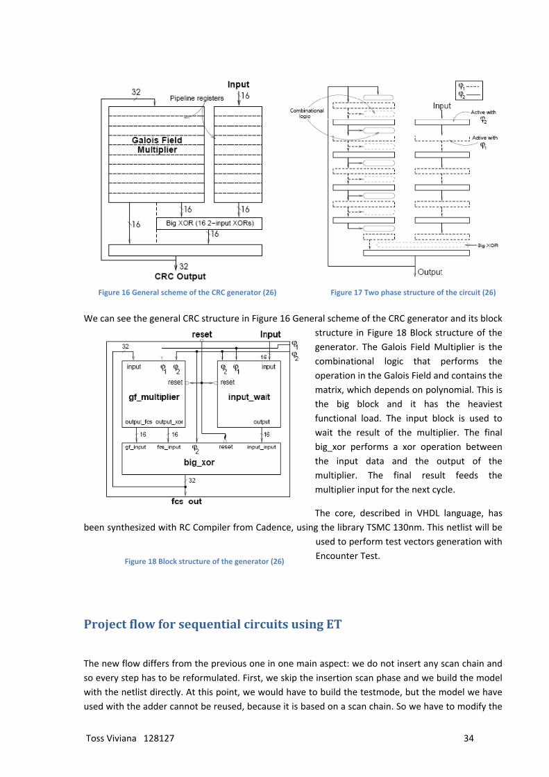
Toss Viviana 128127 34
We can see the general CRC structure in Figure 16 General scheme of the CRC generator and its block structure in Figure 18 Block structure of the generator. The Galois Field Multiplier is the combinational logic that performs the operation in the Galois Field and contains the matrix, which depends on polynomial. This is the big block and it has the heaviest functional load. The input block is used to wait the result of the multiplier. The final big_xor performs a xor operation between the input data and the output of the multiplier. The final result feeds the multiplier input for the next cycle.
The core, described in VHDL language, has been synthesized with RC Compiler from Cadence, using the library TSMC 130nm. This netlist will be
used to perform test vectors generation with Encounter Test.
Project flow for sequential circuits using ET
The new flow differs from the previous one in one main aspect: we do not insert any scan chain and so every step has to be reformulated. First, we skip the insertion scan phase and we build the model with the netlist directly. At this point, we would have to build the testmode, but the model we have used with the adder cannot be reused, because it is based on a scan chain. So we have to modify the
Figure 16 General scheme of the CRC generator (26) Figure 17 Two phase structure of the circuit (26)
Figure 18 Block structure of the generator (26)
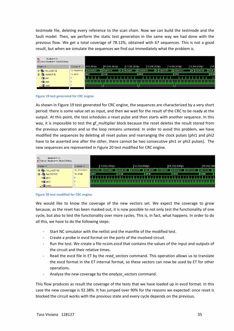
Toss Viviana 128127 35
testmode file, deleting every reference to the scan chain. Now we can build the testmode and the fault model. Then, we perform the static test generation in the same way we had done with the previous flow. We get a total coverage of 78.12%, obtained with 67 sequences. This is not a good result, but when we simulate the sequences we find out immediately what the problem is.
Figure 19 test generated for CRC engine
As shown in Figure 19 test generated for CRC engine, the sequences are characterized by a very short period: there is some value set as input, and then we wait for the result of the CRC to be ready at the output. At this point, the test schedules a reset pulse and then starts with another sequence. In this way, it is impossible to test the gf_multiplier block because the reset deletes the result stored from the previous operation and so the loop remains untested. In order to avoid this problem, we have modified the sequences by deleting all reset pulses and rearranging the clock pulses (phi1 and phi2 have to be asserted one after the other, there cannot be two consecutive phi1 or phi2 pulses). The new sequences are represented in Figure 20 test modified for CRC engine.
Figure 20 test modified for CRC engine
We would like to know the coverage of the new vectors set. We expect the coverage to grow because, as the reset has been masked out, it is now possible to not only test the functionality of one cycle, but also to test the functionality over more cycles. This is, in fact, what happens. In order to do all this, we have to do the following steps:
‐ Start NC simulator with the netlist and the mainfile of the modified test. ‐ Create a probe in evcd format on the ports of the involved circuit. ‐ Run the test. We create a file ncsim.evcd that contains the values of the input and outputs of
the circuit and their relative times. ‐ Read the evcd file in ET by the read_vectors command. This operation allows us to translate
the evcd format in the ET internal format, so these vectors can now be used by ET for other operations.
‐ Analyze the new coverage by the analyze_vectors command.
This flow produces as result the coverage of the tests that we have loaded up in evcd format. In this case the new coverage is 92.38%. It has jumped over 90% for the reasons we expected: once reset is blocked the circuit works with the previous state and every cycle depends on the previous.

Toss Viviana 128127 36
The CRC used till now is very simple and its potential is not completely exploited. The pipeline works on different channels in conformity with time division multiplexing (TDM) principles, but the input cannot be addressed to any particular channel. This CRC works well if there is a data stream that is already arranged.
In order to have a more meaningful case study, we make changes in the CRC structure. We add a channel field to every incoming packet of data that consists of three bits that indicate what channel we want to use. There are 8 registers, one for every channel, that store the state of a specific channel: the result of a cycle is stored in a register corresponding to its channel, basing on the channel information of the data. When there is a new input data of coming from the same channel, the result of the previous cycle is chosen to feeds up the gf_multiplier. In this way, it is possible to use every channel in the order we prefer, without any constraint except for the latency of the operation (we cannot perform a new operation if the last is not yet finished).
The new block diagram of the circuit is shown in Figure 21 Block diagram of the CRC core with 8 channels.
Figure 21 Block diagram of the CRC core with 8 channels
The grey field in input_wait, big_xor and fcs_out blocks represents the channel information. There are two muxes: the first stores the result into the corresponding state register and it is controlled by the fcs_out information field. The second one feeds the gf_multiplier block with the state saved from the previous iteration and it is controlled by the channel field of the incoming data. In this way, it is possible to use channels in the desired order, in agreement with the latency. At the moment we still use the two phase structure, so the global latency is 6 clock pulses.
Now we have to connect this peripheral to a processor able to communicate with it and to control it.
We chose Leon3, a synthesizable VHDL model of a 32‐bit processor, distributed under GNU GPL license and available on the Gaisler web pages. It is distributed as part of a more complete library, the GRLIB IP library. It is also fully parameterizable and it is possible to add or to delete peripheral

Toss Viviana 128127 37
devices, cores, etc. As we can see in Figure 22 Grlib architecture, the GRLIB is composed by several blocks, in addition to the central processor, and all the IP cores are connected by an AMBA 2.0 bus. The processor core, the Leon3, conforms to the IEEE‐1754 architecture, or SPARC (Scalable Processor ARChitecture). SPARC is a CPU instruction set architecture, based on RISC principles. The main features of Leon3 are :
− 7‐stage pipeline with Harvard architecture. − Hardware multiplier and divider. − On‐chip debug support. − Multiprocessor extensions. We are not interested in all Leon3 capabilities, we are going to use this structure mainly because it is available for free and it is interfaced by a standard bus, an AMBA bus.
Figure 22 Grlib architecture (27)
In order to create and connect the CRC block to the Leon3 core we have to develop a wrapper able to communicate with the standard AMBA (Advanced Microcontroller Bus Architecture).
An AMBA‐based microcontroller typically connects CPU and DMA (Direct Memory Access) devices, as external memories, JTAG, USB, Ethernet ports, by a high‐performance system backbone bus (28) . In order to connect lower bandwidth peripheral we use an APB (Advanced Peripheral Bus), that is an interface between the AMBA bus and peripherals with minimal power consumption and reduced interface complexity.
We are not interested in how APB communicates with the AMBA bus; we focus only on the transmission protocol between APB and the peripheral. The state diagram is very
Figure 23 State diagram for APB transfers (28)
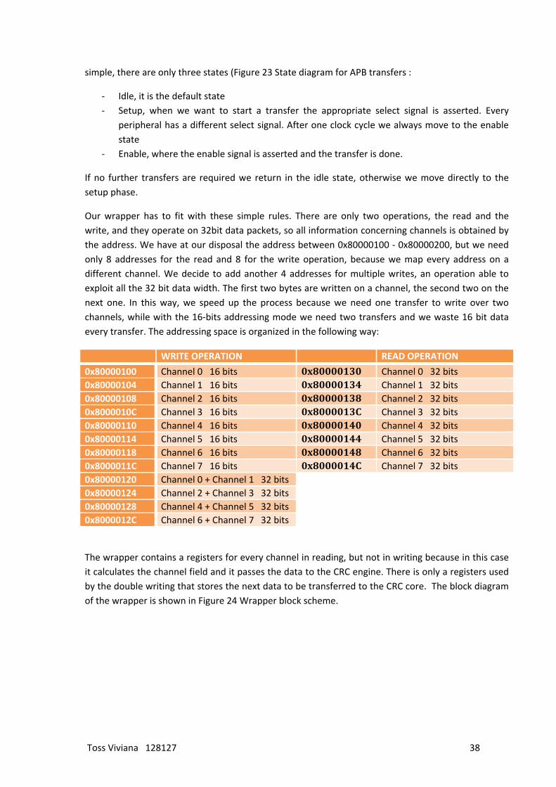
Toss Viviana 128127 38
simple, there are only three states (Figure 23 State diagram for APB transfers :
‐ Idle, it is the default state ‐ Setup, when we want to start a transfer the appropriate select signal is asserted. Every
peripheral has a different select signal. After one clock cycle we always move to the enable state
‐ Enable, where the enable signal is asserted and the transfer is done.
If no further transfers are required we return in the idle state, otherwise we move directly to the setup phase.
Our wrapper has to fit with these simple rules. There are only two operations, the read and the write, and they operate on 32bit data packets, so all information concerning channels is obtained by the address. We have at our disposal the address between 0x80000100 ‐ 0x80000200, but we need only 8 addresses for the read and 8 for the write operation, because we map every address on a different channel. We decide to add another 4 addresses for multiple writes, an operation able to exploit all the 32 bit data width. The first two bytes are written on a channel, the second two on the next one. In this way, we speed up the process because we need one transfer to write over two channels, while with the 16‐bits addressing mode we need two transfers and we waste 16 bit data every transfer. The addressing space is organized in the following way:
WRITE OPERATION READ OPERATION
0x80000100 Channel 0 16 bits 0x80000130 Channel 0 32 bits 0x80000104 Channel 1 16 bits 0x80000134 Channel 1 32 bits 0x80000108 Channel 2 16 bits 0x80000138 Channel 2 32 bits 0x8000010C Channel 3 16 bits 0x8000013C Channel 3 32 bits 0x80000110 Channel 4 16 bits 0x80000140 Channel 4 32 bits 0x80000114 Channel 5 16 bits 0x80000144 Channel 5 32 bits 0x80000118 Channel 6 16 bits 0x80000148 Channel 6 32 bits 0x8000011C Channel 7 16 bits 0x8000014C Channel 7 32 bits 0x80000120 Channel 0 + Channel 1 32 bits 0x80000124 Channel 2 + Channel 3 32 bits 0x80000128 Channel 4 + Channel 5 32 bits 0x8000012C Channel 6 + Channel 7 32 bits
The wrapper contains a registers for every channel in reading, but not in writing because in this case it calculates the channel field and it passes the data to the CRC engine. There is only a registers used by the double writing that stores the next data to be transferred to the CRC core. The block diagram of the wrapper is shown in Figure 24 Wrapper block scheme.

Toss Viviana 128127 39
Figure 24 Wrapper block scheme
Once the wrapper is connected with the bus by some configuration file we have to write the program itself. We use the compiler predisposed in the grlib, msys, and we modify the testbench program that is distributed with the library. In order to create a peripheral we have to instantiate a struct whose fields are the internal registers that we can read or write. The declaration sequence determines the address of the register, so we have to pay attention to declare them in the correct order. An example program could be the following one.
#define CRCADR 0x80000100; struct CRC_wrapper { volatile unsigned int ch0; /* 0x00 */ volatile unsigned int ch1; /* 0x04 */ volatile unsigned int ch2; /* 0x08 */ volatile unsigned int ch3; /* 0x0C */ volatile unsigned int ch4; /* 0x10 */ volatile unsigned int ch5; /* 0x14 */ volatile unsigned int ch6; /* 0x18 */ volatile unsigned int ch7; /* 0x1C */ volatile unsigned int ch0ch1; /* 0x20 */ volatile unsigned int ch2ch3; /* 0x24 */ volatile unsigned int ch4ch5; /* 0x28 */ volatile unsigned int ch6ch7; /* 0x2C */ volatile unsigned int readch0; /* 0x30 */ volatile unsigned int readch1; /* 0x34 */ volatile unsigned int readch2; /* 0x38 */ volatile unsigned int readch3; /* 0x3C */ volatile unsigned int readch4; /* 0x40 */ volatile unsigned int readch5; /* 0x44 */ volatile unsigned int readch6; /* 0x48 */ volatile unsigned int readch7; /* 0x4C */ }; int crc_test(int addr) { struct CRC_wrapper *crc1 = (struct CRC_wrapper *) addr; int correct = 1; int b=0; crc1‐>ch0 = 0x00000000; crc1‐>ch4 = 0x00000080;

Toss Viviana 128127 40
crc1‐>ch7 = 0x0000B27F; b = crc1‐>readch4; if (b != 0xFFFFF7FF) correct=0; // final test if (correct== 1) report_device(0x01011000); else report_device(0x0101a000); }
This is a program example: we write over the bus the values to be transferred to the CRC unit, then we read the result and we compare it with the one we expected. If they are equal all is good, otherwise there is a fault in the CRC unit (presuming the bus is fault free).
Now we have all the elements to create our software test. We synthesize the wrapper and the CRC unit and we follow the same flow presented for CRC in order to create test vectors with ET. Once we have synthesized the netlist we discover that there are some problem with the two phase clock. The netlist does not behave correctly, there are some timing violations and the two phases are not perfectly synchronized. So we decided to use only one clock, we lost in time performance but we do not have any problem with the netlist. Channel0 is also used as trash bin, where we store the unimportant data which should not affect the other channels.
Unfortunately the results we found out with ET are not as good as we expected. The coverage is very low, only 32% and we can see the reasons in Figure 25 test for CRC wrapper.
Figure 25 test for CRC wrapper
The vectors found by ET are not efficient because there are scheduled reset pulses continuously, the addresses are generated in a completely random way and the protocol used by the bus further complicates everything because, in order to write in a specific register, ET has to find out also the protocol communication in addition to find out a valid address.
Problems in general case
Observing these results we understand that this methodology is not as good as we hoped. The vectors found by ET are not “functional” enough and in order to achieve a good coverage there are a lot of handmade modifications that depend on the structure under test. We cannot generalize this

Toss Viviana 128127 41
process for other peripherals because modifications made on the vectors are bound to the functionality of the circuit. If the difference between vectors found by ET and the final vectors with high coverage is so large, there is no need to employ software like ET, and we could randomly generate and adapt them to our case. A possible solution could be teaching ET how a protocol behaves, but this is not a simple solution and until now we have not found it possible. We tried to set some test generation option:
‐ Linehold: it blocks an input to a determinate value. There are both hard and soft lineholds, but any of these solve our problem: the first does not allow resetting the circuit at the beginning of the test sequence, while the second allows resetting the circuit at every sequence. We would like to reset only once, at the beginning of the test.
‐ User’s sequences: it is possible to specify some sequence events, i.e., clock pulses, output control, and input setting. We trust this solution a lot but at the end we find out that these user’s sequences are not used as starting point to generate automatic sequences. ATPG creates its own sequences and then it checks if these are equal to the user’s sequences, if they differ it discards them. This is completely useless in our case, because it is very difficult for ATPG to find out transmission protocol.
In order to increase the sequential depth of the circuit, we try to space out two consecutive reset pulses. We transform our circuit by adding a shift register in output, whose depth consists of 50 registers. The schematic is shown in Figure 26 CRC and shift register.
We follow the same flow described previously and then we obtain that sequences are longer, as we can see in Figure 27. We map these sequences to a C software and we simulate them.
Figure 27 Sequence example
We dump the simulation and we read them in ET. We analyze them and we obtain a total coverage of 92,84%, if we include also precollapsed faults (i.e., input faults equivalent to one of the output fault of the same block) we obtain 94,51%.
Despite ET limitations and our difficulties, we have finally designed a project flow that is able to detect more than 92% of the faults. This is a good result, because the tool used is a commercial tool, mainly conceived to solve circuit with scan chain insertion, and it is applied in a totally different context.
Figure 26 CRC and shift register

Toss Viviana 128127 42
Safety critical systems
In this chapter we introduce some new concepts used in the second section of the thesis: safety critical systems, risk, reliability and the IEC 61508 standard.
According to German sociologist Ulrich Beck, a different relationship with risk marks today’s society in comparison with all the previous societies. Before the industrial and technological advancements the hazards came from the external world, but now “the risk society is characterized essentially by a lack: the impossibility of an external attribution of hazards. In other words, risks depend on decisions, they are industrially produced and in this sense politically reflexive”(29). In order to protect people and the environment from these new technological hazards we use a lot of safety systems, consisting of computer‐based systems, and so subject to technological risks. The problem is how to rely on these safety systems and how to find a measure for their reliability. In order to answer these questions many standards have been proposed in the last years, and among them we will analyze the international standard for safety systems IEC 61508.
In order to analyze these topics we need to understand some basic concepts, such as safety, risk, reliability, that we introduce in the following section.
Safety barriers
Safety is a concept for which everyone has a general understanding; however, it has extensive ramifications and it is hard to find a definition able to include its many aspects. Commonly, safety means the protection of human life, health, the environment, and businesses against undesirable hazards. According to IEC 61508 standard, safety is “freedom from unacceptable risk of physical injury or of damage to the health of people, either directly, or indirectly as a result of damage to property or to the environment”(5). A similar concept, functional safety, is defined in the same standard as “part of the overall safety that depends on a system or equipment operating correctly in response to its inputs”. Both safety and functional safety cannot be interpreted with reference only to the system under analysis, but it is compulsory to consider “the systems as a whole and the environment with which they interact”.
In order to apply this productive process and to understand if a system, or process, is safer than another, we need a measure, qualitative or quantitative, of the achieved risk reduction. There are many models to describe this situation; the most common are the energy model and the process model.
The energy model was introduced in 1961 by Gibson (2) and subsequently extended by Haddon (3). It is based on the separation between hazards (or energy sources) from victims (vulnerable targets) by safety barriers. Another perspective is adopted in the process model (30), where accident sequences
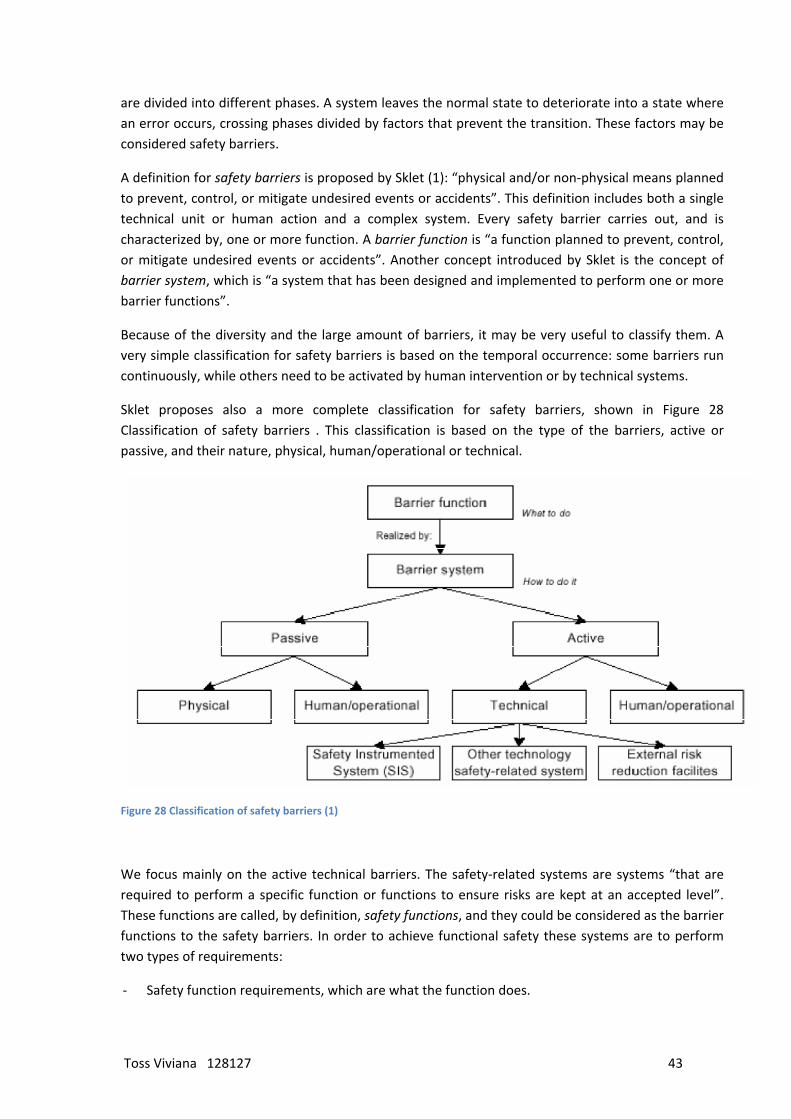
Toss Viviana 128127 43
are divided into different phases. A system leaves the normal state to deteriorate into a state where an error occurs, crossing phases divided by factors that prevent the transition. These factors may be considered safety barriers.
A definition for safety barriers is proposed by Sklet (1): “physical and/or non‐physical means planned to prevent, control, or mitigate undesired events or accidents”. This definition includes both a single technical unit or human action and a complex system. Every safety barrier carries out, and is characterized by, one or more function. A barrier function is “a function planned to prevent, control, or mitigate undesired events or accidents”. Another concept introduced by Sklet is the concept of barrier system, which is “a system that has been designed and implemented to perform one or more barrier functions”.
Because of the diversity and the large amount of barriers, it may be very useful to classify them. A very simple classification for safety barriers is based on the temporal occurrence: some barriers run continuously, while others need to be activated by human intervention or by technical systems.
Sklet proposes also a more complete classification for safety barriers, shown in Figure 28 Classification of safety barriers . This classification is based on the type of the barriers, active or passive, and their nature, physical, human/operational or technical.
Figure 28 Classification of safety barriers (1)
We focus mainly on the active technical barriers. The safety‐related systems are systems “that are required to perform a specific function or functions to ensure risks are kept at an accepted level”. These functions are called, by definition, safety functions, and they could be considered as the barrier functions to the safety barriers. In order to achieve functional safety these systems are to perform two types of requirements:
‐ Safety function requirements, which are what the function does.

Toss Viviana 128127 44
‐ Safety integrity requirements, which measure the likelihood of a safety function being performed satisfactorily.
Between active technical barriers, a distinct class is formed by the safety instrumented systems (SIS). These are computer‐based barriers, very complex but also very powerful, and they will be discussed in the following.
Risk
The purpose of barrier systems and safety barriers is to reduce risk, but we have not yet defined the concept of risk. As a matter of fact, this concept is very complex because it has both a positive and a negative value, and it is strongly correlated with the concept of uncertainty.
The risk definition provided by the Society for Risk Analysis is: “the potential for realization of unwanted, adverse consequences to human life, health, property, or the environment; estimation of risk is usually based on the expected value of the conditional probability of the event occurring times the consequence of the event given that it has occurred”. (31)
The IEC 61508 standard defines risk as a “combination of the probability of occurrence of harm and the severity of that harm”. (5)
Safety barriers could reduce risk in two main ways: either they reduce the probability that hazard occurs or they reduce the severity of the harm. These two different aspects are both important and it is practically impossible to determine which should be prioritized.
It is impossible to achieve total safety, so in order to define if a system is to be considered safe or not two principles are often applied:
‐ ALARP: as low as reasonably practicable. ‐ ALARA: as low as reasonably achievable.

Toss Viviana 128127 45
Figure 29 ALARP concept (5)
In Figure 29 ALARP concept , the ALARP concept is discussed: it is in the middle between the negligible risk and the intolerable region. It is an arrangement between the benefit we would desire and the cost we would have to tolerate in order to achieve it. The diminishing proportionality between effort and risk reduction is described with a triangle, if the cost is out of proportion to the benefit we tolerate the risk we have if it is, at least, in the tolerable region. The ALARP concept is widely used in the IEC 61508 standard.
Safety instrumented systems
Safety instrumented systems are active technical barriers and they are defined as computer‐based safety systems composed of sensors, logic solvers and actuating items. Their purpose is to mitigate the risk associated with the equipment under control (EUC). This terminology has been defined as “equipment, machinery, apparatus or plant used for manufacturing, process, transportation, medical or other activities” in IEC 61508. (5)
In the IEC 61508 standard a safety instrumented system is referred to as an “electrical/electronic/programmable electronic (E/E/PE) safety‐related system” (5), defined in the same standard as a “system for control, protection or monitoring based on one or more electrical/electronic/programmable electronic (E/E/PE) devices, including all elements of the system such as power supplies, sensors and other input devices, data highways and other communication paths, and actuators and other output devices”. (5)

Toss Viviana 128127 46
Reliability of safety systems
A general definition for reliability is given by the ISO 8402 standard: “Reliability is the ability of an item to perform a required function, under given environmental and operational conditions and for a stated period of time”. The reliability of a safety system can so be expressed as the ability to perform its safety functions, under given environmental, operational and temporal conditions. When a failure to perform this function occurs, it is called a fail to function (FTF), and it is one of the main problem in safety systems. The other is the spurious trip (ST) and it happens when the safety system is activated without the presence of the relative hazard. In other word, it is a false alarm, and it could be very dangerous because safety systems usually are very autonomous and they are able to shut down safeguard processes or to restart other systems, leaving the EUC in an unstable situation. Moreover they increase costs and reduce the confidence in the systems.
In term of FTF, it is possible to divide safety systems in two distinct classes: low demand mode safety systems and high demand mode safety systems. A system that rarely experiences failures, e.g., less than once per year, belongs to the low demand mode. They are characterized by the average probability of failure on demand (PFD). On the contrary, the safety systems that are continuously used belong to the high demand mode, and the measure used in this class is the probability of a dangerous failure per hour (PFH). (32)
In order to achieve a reliability certification of safety systems, many standards have been proposed. The first, as the German standard DIN 19250 proposed in 1994, are product‐oriented and give detailed, technology dependent design requirements. In order to achieve the certification, there are several qualitative analyses to be performed, as hardware tests, expert experience and design guideline.
At the end of the century a new trend gained ground: the use of quantitative techniques and the focus on the entire lifetime of the product. Examples of these new standards are ISA‐SP84 of the Instrumented Society of America and IEC 61508 of the International Electrotechnical Commission. They require quantification of the achieved risk reduction, not only qualitative opinions, and they do not suggest precise technical requirements, but only provide a general framework for the design and the implementation.
Some techniques, both qualitative and quantitative, are suggested in these standards. Among the qualitative techniques, we find:
- Expert analysis: it is based on previous experiences with similar systems. The German DIN standards rely heavily on this analysis, which has the advantage that previous experience is used, but this experience may be invalid for completely new systems.
- Failure mode and effects analysis (FMEA): it is a bottom up analysis and it examines all possible component failures and it determines the effect of these failures.
- Hazard and operability study: it provides a prioritized basis for the implementation of risk mitigation strategies.
Examples of quantitative techniques are:

Toss Viviana 128127 47
- Parts count analysis: the failure rate of a system is equal to the sum of all failures rates of the individual components. This technique is very simple but it does not take into account redundancy and testing.
- Reliability block diagram: it consists of functional blocks that graphically show the condition for successful operation, and it take into account redundancy.
- Fault tree analysis: is a top‐down analysis that graphically finds the causes that can lead to a defined undesirable event.
- Markov models: it describes a system using a set of mutually exclusive states and transition between states. It gives exactly the same results as classical probability techniques.
Failure classification
In order to achieve a good quality of a reliability analysis, it is important to identify all the required functions of the system, and this may be very difficult because a single system could have to perform many functions. A failure is the event when a required safety function is terminated and the safety system fails to perform it. According to the IEC 60050‐191 standard (33), this concept should not be confused with the concept of error and of fault. An error is a “discrepancy between a computed, observed or measured value or condition and the true, specified or theoretically correct value or condition”. (33) A fault is “the state of an item characterized by inability to perform a required function, excluding the inability during preventive maintenance or other planned actions, or due to lack of external resources” and so it is a state resulting from a failure. This relationship is shown in Figure 30 Relationship between failure, fault and error.
Figure 30 Relationship between failure, fault and error
Failures are often classified into failure models, which are the description of a fault. To identify all the possible failure modes could be harder than to identify all the functions of a system, because every function can have more than one failure mode. It is also impossible to determine the relationship between faults and failures. However, it is important to classify and to characterize failures in order to achieve better results in:
‐ Avoiding failures during the different phases of the lifecycle. ‐ Controlling failures during operation.

Toss Viviana 128127 48
A first division is based on the time of origin of the failure (5):
‐ Failures can be caused by faults originating before or during system installation. ‐ Failures can be caused by faults or human errors originating after system installation.
Another possible way to classify failures is presented by Henley and Kumamoto (34):
‐ Primary failures: they are caused by natural aging of the item. ‐ Secondary failures: they are caused by excessive stresses outside the design envelope. ‐ Command faults: they are caused by inadvertent control signals or noise.
Another classification is proposed by Blanche and Shrivastava (35) and is shown in Figure 31 Failure mode classification according to Blanche and Shrivastava.
Figure 31 Failure mode classification according to Blanche and Shrivastava
The temporal length is the first classification: an intermittent failure last only for a very short time, while an extended failure continues until replacement or repair of the system. The second fork is based on the extension of the failure: if a failure fails the required function completely is a complete failure, otherwise it is a partial failure. The temporal evolution is the third branch: a failure can be gradual or sudden. For two failures specific names are provided: complete sudden failures are called catastrophic, partial gradual failures are called degraded failures.
Another classification determines whether failures are detected or not in tests. Safety instrumented systems usually have the possibility to perform automatic self‐tests in order to maintain a control on the state of the system. These tests are called diagnostic tests but they are not able to detect the totality of the failure modes. The fraction of failure revealed by diagnostic tests is called diagnostic coverage factor, while the other failures are defined undetected.
In order to achieve a greater coverage functional tests are performed offline at regular time intervals.

Toss Viviana 128127 49
Failures can also be dependent and have a common cause. This could results from the high degree of redundancy typical of safety systems. In fact redundancy improves reliability but introduces the so‐called common cause failures, and it reduces the positive effect of redundancy. The IEC 61508 defines a common cause failure as a “failure, which is the result of one or more events, causing coincident failures of two or more separate channels in a multiple channel system, leading to system failure”.(5)
The IEC 61508 standard divides the failures into two main categories basing on their causes:
‐ Random hardware failures: they result from natural degradation mechanisms in the hardware. They occur at predictable rates but unpredictable times; this is because there are many degradation mechanisms occurring at different rates in different components and components fail after different times in operation.
‐ Systematic failures: they are “related in a deterministic way to a certain cause, which can only be eliminated by a modification of the design or of the manufacturing process, operational procedures, documentation or other relevant factors”(5). They could be caused by human errors in the safety requirements specification, in the design of the hardware of the software, etc.
The greater difference between random hardware failures and systematic failures is that “system failure rates arising from random hardware failures can be quantified with reasonable accuracy but those arising from systematic failures cannot be accurately statistically quantified because the events leading to them cannot easily be predicted”.
There is also another famous subdivision presented in IEC 61508: safe and dangerous failures. We will analyze these classes deeply in the following, after a brief introduction on IEC 61508 standard.
IEC 61508
IEC 61508 is the currently standard for safety instrumented systems. It is general, it does not prescribe specific technologic requirements but it describes a framework and it focus on lifetime cycle. More precisely IEC 61508:
‐ It uses a “risk based approach to determine the safety integrity requirements of E/E/PE safety‐related systems”. Safety integrity means the ability of the SIS to perform its intended safety functions.
‐ It uses an “overall safety lifecycle model as technical framework”. This means that, when we develop the safety requirements for a SIS we also take into account the contributions from safety systems based on other technologies and from external risk reduction facilities. This reflects the idea that it is impossible to talk about safety of a system without considering all the conditions and the environment that characterized it.
‐ It covers all the lifecycle of the EUC, from the initial concept to final decommissioning. It covers all the phases of hazard analysis and risk assessment, development of the safety requirements, specification, design and implementation, operation and maintenance, and modification
‐ It contains requirements in order to prevent and to control failures. ‐ It specifies the techniques and measures necessary to achieve the required safety integrity.

Toss Viviana 128127 50
As we can see there is not a specific field action, but the standard is technology independent and could be applied in different applications. It is not prescriptive, so new solutions, methods, approaches or technologies, if they meet the requirements, can be used.
The final purpose is to reduce the risk of the EUC under a determinate threshold that is application dependent. This threshold, the tolerable risk, is referred to a specific hazardous event and it is determinate with respect to the frequency (or probability) of the event and to its consequences. SISs have to be designed in order to reduce the probability of hazards and/or the undesired consequences. The concept of risk reduction is shown in Figure 32 Risk reduction: general concepts.
Figure 32 Risk reduction: general concepts
It is important to underline the difference between risk and safety integrity. The first, in this specific case the tolerable risk, depends on a lot of factors, social and political. The safety integrity is related “solely to the E/E/PE safety‐related systems, other technology safety related‐systems and external risk reduction facilities and is a measure of the likelihood of those systems/facilities satisfactorily achieving the necessary risk reduction in respect of the specified safety functions”. As we can see in Figure 32 Risk reduction: general concepts, we first determine the tolerable risk, and then we estimate the EUC risk and calculate the necessary risk reduction. At this point it is possible to determine the safety integrity requirements for the safety‐related systems in order to achieve, and possibly to go over, the threshold of tolerance.
The technical framework proposed by the IEC 61508 standard is shown in Figure 33 Overall safety lifecycle , and it is composed of the following phases:
‐ Phase 1 – CONCEPT: we have to analyze and understand the EUC and its environment. ‐ Phase 2 – OVERALL SCOPE DEFINITION: we have to determine the boundary of the EUC and of
the EUC control system, in order to specify the scope of the risk analysis.

Toss Viviana 128127 51
‐ Phase 3 – HAZARD AND RISK ANALYSIS: we have to determine all the hazardous events of the EUC, the event sequences leading to them and the EUC risk associated with them.
‐ Phase 4 – OVERALL SAFETY REQUIREMENTS: we have to develop the safety functions requirements and the safety integrity requirements for all the safety‐related systems in order to achieve the required functional safety.
‐ Phase 5 – SAFETY REQUIREMENTS ALLOCATION: we have to allocate the safety function requirements and the safety integrity requirements to E/E/PE safety related systems, other technology safety‐related systems and external risk reduction facilities.
‐ Phase 6 – OVERALL OPERATION AND MAINTENANCE PLANNING: we have to describe a plan in order to ensure that the required functional safety function is performed during operation and maintenance.
‐ Phase 7 – OVERALL SAFETY VALIDATION PLANNING: we have to develop a plan in order to achieve the overall safety validation of the E/E/PE safety‐related systems.
‐ Phase 8 – OVERALL INSTALLATION AND COMMISSIONING PLANNING: we have to develop a plan in order to ensure that the required functional safety function is performed during installation and commissioning.
‐ Phase 9 – E/E/PE SAFETY‐RELATED SYSTEMS REALISATION: we have to create the E/E/PE safety‐related systems conforming to the specifications (i.e., safety function and safety integrity requirements) given in the previous points.
‐ Phase 10 – OTHER TECHNOLOGY SAFETY‐RELATED SYSTEMS REALISATION: we have to create the other technology safety‐related systems conforming to the specification given in the previous points. This point is not discussed in the IEC 61508 standard.
‐ Phase 11 – EXTERNAL RISK REDUCTION FACILITIES REALISATION: we have to create the external risk reduction facilities conforming to the specification given in the previous points. This point is not discussed in the IEC 61508 standard.
‐ Phase 12 – OVERALL INSTALLATION AND COMMISSIONING: we have to install and to commission the E/E/PE/safety‐related systems, according to plan described in phase 8.
‐ Phase 13 – OVERALL SAFETY VALIDATION: we have to verify that the E/E/PE/safety‐related systems meet all the requirements in terms of safety function and safety integrity requirements, according to plan described in phase 7 and taking into account the allocation chosen in phase 5.
‐ Phase 14 – OVERALL OPERATION, MAINTENANCE AND REPAIR: we have to operate, maintain and repair the E/E/PE/safety‐related systems, according to plan described in phase 6.
‐ Phase 15 – OVERALL MODIFICATION AND RETROFIT: we have to ensure that functional safety is appropriated during and after the modification.
‐ Phase 16 – DECOMMISSIONING OR DISPOSAL: we have to ensure that functional safety is appropriated during and after the activities of decommissioning or disposing of the EUC.

Toss Viviana 128127 52
Figure 33 Overall safety lifecycle (5)
The IEC 61508 standard is not only based on qualitative measures, but it inserts also quantitative steps in order to propose an order concerning how good a safety‐related system is. The most important classification is based on safety integrity and defines four levels called safety integrity levels (SIL). The SIL1 has the lowest safety integrity while the SIL4 the highest. SIL can be applied only to an entire system, so it is not correct to refer it to an individual item, such a sensor, because the safety function is performed by the whole system. In order to determine in a quantitative way which level a EUC belongs to, we have to calculate the probability of failure on demand (PFD) if the system operates in low demand mode, or the probability of dangerous failure per hour (PFH) if the system operates in high demand mode. The standard proposes also qualitative methods to determine the SIL, as the risk graph and the hazardous event severity matrix. In Table 1 Safety integrity level the

Toss Viviana 128127 53
classification based on quantitative method is shown for both operating modes. It could be important to determine the SIL of a EUC because some applications require a quality level higher than others and it would be impossible to manage industrial safety processes on the basis of qualitative classifications only.
Safety integrity level
Low demand mode of operation (Average probability of failure to perform its
design function on demand)
High demand or continuous mode of operation
(Probability of a dangerous failure per hour)
4 10 10 10 103 10 10 10 102 10 10 10 101 10 10 10 10
Table 1 Safety integrity level (5)
In order to achieve a realistic interpretation of the danger of a hazardous event we have to consider both its consequences and its frequency. It is possible to classify a hazardous event into risk classes matching its consequences with its tolerable frequencies. This classification is based on ALARP concept and it deals with the residual risk after the risk reduction measures have been put in place. The four risk classes are:
‐ Class I: intolerable risk. ‐ Class II: undesirable risk. It is tolerable “only if risk reduction is impracticable or if the costs are
grossly disproportionate to the improvement gained”(5). ‐ Class III: tolerable risk if the cost of risk reduction would exceed the improvement gained. ‐ Class IV: negligible risk.
As we can see in Table 2 Example of risk classification for accident, a consequence could be tolerable or not based on its frequency. In this case we deal with risk classification for accident. A marginal consequence can be considered intolerable if the event is frequent, while if the event is probable we can consider it as undesirable.
Table 2 Example of risk classification for accident

Toss Viviana 128127 54
The IEC 61508 standard gives also an overview of the principal techniques and measures used to achieve the safety requirements. The proposed methods cover all the possible safety problems in an E/E/PE safety‐related system, from the electrical/electronic problems to the supply power, ventilation and heating problems.
In order to control random hardware failures in solid‐state components (i.e., electronic hardware failures, which is our case) the standard proposes several approaches, some of these are:
- Tests by redundant hardware: it uses hardware redundancy, i.e., “additional hardware not required to implement the process functions” (5)
- Standard test access port and boundary –scan architecture: it is based on scan chain insertion
- Monitored redundancy: in this approach the safety function is executed by at least two hardware channels. The output of each channel is monitored in order to detect different behaviors
- Electrical/electronic components with automatic check: it detects faults testing the hardware before the process starts and it repeats the test at defined intervals
- De‐rating: it is “the practice of ensuring that under all normal operating circumstances, components are operated well below their maximum stress level”.(5)
There are also specific methods for processing units, sensors, memories, etc.
The standard does not give technical requirements, as we already said, but it sets out requirements for both hardware and software of a safety instrumented system. These requirements refer to failure probability, hardware fault tolerance, avoidance and control of systematic faults. The standard does not provide specific methods to guarantee the conformance, but for each SIL it identifies some constraints as safe failure fraction, that we analyze in the following, or other measures to avoid systematic faults.
Safe and dangerous failures As previously mentioned, the IEC 61508 standard classifies failures according to their effects distinguishing between safe and dangerous failures. A dangerous failure is “failure which has the potential to put the safety‐related system in a hazardous or fail‐to‐function state”(5), while a safe failure is a failure that has not this potential and that leads “to the safety integrity of an E/E/PE safety‐related system not being compromised”(5). Often this classification is combined with the detected/undetected one. This subdivision is useful to calculate two other quantities: ‐ Diagnostic coverage (DC): “fractional decrease in the probability of dangerous hardware failures
resulting from the operation of the automatic diagnostic tests”. In other words, it is the fraction of the dangerous failures detected by an automatic test over the totality of dangerous faults. It could be referred to the whole system or to a single part. The diagnostic coverage is represented with the following equation, where represents the probability of detected dangerous failures and is the probability of total dangerous failures.
∑
∑

Toss Viviana 128127 55
‐ Safe failure fraction (SFF): “the ratio of the average rate of safe failures plus dangerous detected
failures of the subsystem to the total average failure rate of the subsystem”(5). It may alternatively be defined as the conditional probability that a failure is either a safe failure or a detected dangerous failure (when we know that a failure has occurred). (36) The equation is the following, where represents the rate of detected dangerous failures and is the rate of dangerous failures and is the rate of safe failures.
∑ ∑∑ ∑
These two quantities are important because the IEC 61508 standard provides several requirements for them, in order to allocate a system to a determinate SIL. The steps to calculate them are:
‐ Carry out the effect analysis to determine the consequences of each failure mode of each component of the E/E/PE safety‐related systems in the absence of diagnostic tests. In order to perform this analysis several pieces of information are required, as a detailed block diagram, the hardware schematics, the failure modes and rates of each component, etc.
‐ Categorize each failure as a safe failure or a dangerous failure. ‐ Calculate the probability of safe failure, , and the probability of dangerous failure, , for each
component. ‐ Estimate the fraction of dangerous failures detected by the diagnostic tests, . ‐ Calculate the total probability of dangerous failure, ∑ , the total probability of safe failure,
∑ , and the total probability of dangerous failure detected by the diagnostic tests, ∑ . ‐ Calculate the diagnostic coverage of the system as
∑
∑
‐ Calculate the safe failure fraction of the system as
∑ ∑∑ ∑
The diagnostic test used to detect a dangerous failure can be implemented by another subsystem in the same E/E/PE safety‐related system, and it may operate continuously or periodically.
What we are going to do
Our purpose is to apply a simple solution to a peripheral in order to study these safety problems. We start from a schematic of a peripheral. We chose to test it by redundant hardware, a technique proposed in the IEC 61508 standard. The aim is to control the correct behavior of our peripheral without observing the output. We find a block able to pick up information useful to control the correct behavior of our peripheral. We analyze how this solution works by following these steps:

Toss Viviana 128127 56
‐ We connect our peripheral with the control block, and then we insert them into a structure able to pilot and read them, i.e. a microprocessor.
‐ We execute several programs, possibly typical for the application we are studying. ‐ We simulate these programs and we dump the inputs with NC simulator. ‐ We analyze these inputs with Encounter Test and we find the coverage for our peripheral. This
technique is called fault grading. ‐ We compare this coverage with the coverage we have if we could gain access to peripheral
output and we calculate the diagnostic coverage.
The case study we chose is a pulse width modulation (PWM). It is a very simple peripheral and it is characterized mainly by two parameters: the period and the duty cycle. It is possible to control the correct behavior by testing these two parameters, so we decide to use a timer as control block. The timer is connected with the PWM and it has to measure the period of the entire waveform and the period when the signal is high. The processor reads these data from the timer and we obtain a loop‐back control. In the next chapter we will present the schematics used and their characteristics.

Toss Viviana 128127 57
Fault grading
In this chapter we present the main activity of the thesis: a fault grading flow in order to test a simple case study, a PWM peripheral. We will present the architecture used, the fault grading flow and the results obtained.
In this chapter, we will use two microprocessor peripherals, a Pulse Width Modulation (PWM) and a timer block, to test and develop our fault grading flow. Both for PWM and for the timer blocks, we use the architecture provided by STMicroelectronics within the ARM7TDMI processor.
The PWM block diagram is shown in Figure 34 PWM block diagram. It is very simple and it is possible to activate more than one PWM channel by implementing several modules.
Figure 34 PWM block diagram (37)
In addition to the configuration registers, the architecture includes two prescaler registers, the period register and the duty cycle register. The trig_pwm output is not used.
The timer architecture is much more complex and it is shown in Figure 35 Timer block diagram . It is a 16‐bit programmable timer that can work in many modes, including pulse length measurement of up to two input signals, or generation of output waveforms.
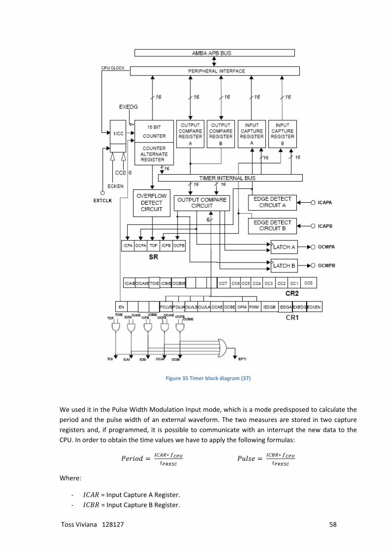
Toss Viviana 128127 58
Figure 35 Timer block diagram (37)
We used it in the Pulse Width Modulation Input mode, which is a mode predisposed to calculate the period and the pulse width of an external waveform. The two measures are stored in two capture registers and, if programmed, it is possible to communicate with an interrupt the new data to the CPU. In order to obtain the time values we have to apply the following formulas:
Where:
‐ = Input Capture A Register. ‐ = Input Capture B Register.

Toss Viviana 128127 59
‐ = internal clock frequency. ‐ = timer clock prescaler.
It is possible to transform the pulse data into the duty cycle data because
In order to simplify the structure as much as possible we do not use the prescaler registers and we reutilize the Leon core previously proposed for the CRC application. We have to connect the two blocks to the AMBA bus, in the same way that is done with the CRC peripheral. The other connection is the loop back between the PWM output and the timer input, as we can see in Figure 36 Connections between PWM‐timer‐AMBA bus.
In order to connect the unit composed by the PWM and the timer to the bus in the most general way we have to implement a wrapper. This wrapper is useful to decouple the input and output type of the PWM and the timer from the types apbi and apbo, characteristic of our implementation of AMBA bus. We can see it in Figure 37 Wrapper for PWM and timer.
Figure 36 Connections between PWM‐timer‐AMBA bus

Toss Viviana 128127 60
Figure 37 Wrapper for PWM and timer
The peripheral created in such way needs two bus channels, so the CPU can communicate in a separate way with both blocks. This wrapper has been synthesized with RTL compiler to obtain a netlist that can be analyzed by Encounter Test and that can be simulated with the Leon3 processor. The pwmout output is hidden when we want to control the coverage obtained by the loop back timer, while when we want to calculate the coverage observed by the PWM output this output is left in the netlist. Once we have the netlist and we connect it to the Leon3 processor we are ready to jump to the next phase. We want to observe how different could be to test the peripheral by the loop‐back control and by the pwm_output. In order to do this we write a program for the Leon3 that performs several operations on the PWM and we analyze with ET if there are differences between the two cases in terms of coverage.
#define PWMADR 0x80000900; #define TMRADR 0x80000300; struct pwm { volatile unsigned int prs0; /* 0x00 */ volatile unsigned int prs1; /* 0x04 */ volatile unsigned int pen; /* 0x08 */ volatile unsigned int pls; /* 0x0C */ volatile unsigned int cpi; /* 0x10 */ volatile unsigned int im0; /* 0x14 */ volatile unsigned int im1; /* 0x18 */ volatile unsigned int dut; /* 0x1C */ volatile unsigned int per; /* 0x20 */ volatile unsigned int rst; /* 0x24 */ }; struct eft { volatile unsigned int icr1; /* 0x00 */
Address of PWM and timer peripherals PWM registers, where: dut = duty cycle register per = period register pen = enable register rst = reset Timer registers, where:

Toss Viviana 128127 61
volatile unsigned int icr2; /* 0x04 */ volatile unsigned int ocr1; /* 0x08 */ volatile unsigned int ocr2; /* 0x0C */ volatile unsigned int cnt; /* 0x10 */ volatile unsigned int cr1; /* 0x14 */ volatile unsigned int cr2; /* 0x18 */ volatile unsigned int sr; /* 0x1C */ volatile unsigned int rst; /* 0x20 */ }; int pwm_routine (int dut, int per,struct pwm *pwm1, struct eft *eft1); int pwm_test(int addr) { struct pwm *pwm1 = (struct pwm *) addr; struct eft *eft1 = (struct eft *) TMRADR; pwm1‐>rst = 0x0000000; eft1‐>rst = 0x0000000; pwm1‐>rst = 0x0000001; eft1‐>rst = 0x0000001; pwm_routine_l (0x0001, 0x0002,pwm1, eft1); } int pwm_routine (int dut, int per,struct pwm *pwm1, struct eft *eft1){ int b=0; int contr =0; int tmp = 0; pwm1‐>dut = dut; pwm1‐>per = per; pwm1‐>pen = 0x00000001; eft1‐>cr1 = 0xC004; b=0; contr = 1; for (tmp=0; tmp<2; tmp++) { while(1){ b = eft1‐>sr; if( b == 0xB000 || b == 0x9000 ) {break;} }; if(tmp == contr) { b = eft1‐>icr1; b = eft1‐>icr2; } eft1‐>sr = 0x0007FFF; } eft1‐>cr1 = 0x4004; }
cr1 = control register 1 icr1 = input capture register 1 icr2 = input capture register 2 sr = status register rst = reset Reset the two peripherals. PWM routine needs the duty cycle value, the period value and the pointers to the PWM and timer structs. Set the period and the duty cycle. Enable the PWM. Set the timer in PWM input mode and start it. Cycle a predefined number of PWM cycle. Control the status of the timer and wait until it achieves a complete measure. Control how many cycle are passed. Read icr1 and icr2. Restart the timer. Stop the timer.

Toss Viviana 128127 62
The structure of the program is very simple and is very easy to handle: after the initialization and the reset of the two peripherals, a routine is called. This routine shows a complete behavior of the PWM, i.e., all the operations that PWM needs to work. In the following we will call PWM frame the interval between two different configurations of the PWM, during which the waveform generation is enabled. The pwm_routine lasts one PWM frame and performs these steps:
‐ It sets the duty cycle and the period value into the PWM internal registers and it enables the PWM.
‐ It sets the control registers of the timer in order to put it in the PWM input mode and it enables the waveform generation.
‐ The cycle managed by tmp variable is used to control how many PWM periods we want to perform in a PWM frame.
‐ By reading the status register of the timer we know when the timer has reached a complete measure, i.e., when a PWM waveform has been completed.
‐ We perform the reading of the loop back timer in a predefined way by comparing the index of the PWM cycle with some constant, in this case the contr variable. In this way we can read the loop back values every cycle or only once for every PWM frame or whenever we want.
‐ It stops the timer when all the PWM cycles have been performed.
Once we write the program the flow is very similar to the one followed in the CRC case study:
‐ We compile the program in order to obtain the file for the memory of the leon3 processor (more precisely for the prom (programmable read only memory), the sram (static random access memory) and the sdram (synchronous dynamic random access memory).
‐ We perform a simulation of the program by using the NC simulator, by Cadence. We dump the input tracks of the synthesized PWM‐timer block in evcd format.
‐ We read the evcd file with Encounter Test, paying attention to set the “Add measures on cycle boundaries” option. This option inserts at every input change an output measure, while if not set the measures are scheduled only when the evcd file indicates a change in an output variable. This was a problem for our application, because in a PWM we have to control that the output signal changes value at the correct instant, but also that the output signal remains stable between the two fronts. We spent some time to understand that the coverage of the first experiments is very low for this reason, which is due to the nature of the evcd format.
‐ We build a testmode in Encounter Test and we build a fault model. In our experiments we consider only static faults.
‐ We analyze the vectors by Encounter Test and we obtain the coverage for the block synthesized, composed by PWM and timer.
‐ In order to obtain the coverage for the PWM block only, we print the statistics relative to only the PWM block by the Report fault statistics command (Figure 38 Report statistics window).

Toss Viviana 128127 63
Figure 38 Report statistics window
This flow has given us excellent results that now we are going to present. The tests performed can be divided into four categories that analyze how the diagnostic coverage changes studying different aspects of this technique:
‐ Read the loop back timer information only once but at different time in a PWM frame. ‐ How many reads have to be performed to obtain a high diagnostic coverage. ‐ The rate that has to be used in a typical application. ‐ Shorted nets faults.

Toss Viviana 128127 64
Experiment 1: read at different time instant
In the system we have implemented, the control hardware is always working but the reading of the data cannot be performed very frequently, because it costs both in time and resources. It is important to find a tradeoff between the cost and the diagnostic coverage. This first experiment wants to analyze if there is any difference in reading the control data at different times. The measure chosen as quality index for the fault grading is the diagnostic coverage, which we have defined in the previous chapter. We can calculate the diagnostic coverage in a simplified way as the fraction of the dangerous failures detected over the totality of dangerous faults. In this system a fault can be considered dangerous if it is able to change the output value. This concept cannot be untied from the application that we are performing: a fault in a register can be dangerous in an application but it could be safe in another that does not read or write this specific register. Our idea is to execute the same program with the two netlists, the one with the pmwout active and the other with this output deleted. In the first case we observe only the PWM output and we execute the program without any read on the control hardware: the faults that can be observed by the pwmout are dangerous, because they can modify the output of the peripheral, while the others can be considered safe, because there is not any visible effect on the output behavior. We do not perform any reading in order to have the measure referred only to the output of the PWM, without taking into account faults that can be referred to the connections with the bus. When we execute the program with the second netlist we cannot observe the PWM output, because it is an internal signal, so any information has to be filtered by the presence of the timer. The faults that can be detected also in this way can be considered as dangerous detected faults. So, if we indicate the first case with the index 1 (i.e., with the pwmout) and with the index 2 the case with the control performed by the timer, we obtain:
∑
∑# #
# #
where is the total coverage, that is the fraction of the detected faults over the total faults.
In this way we can calculate the diagnostic coverage directly from the data provided by Encounter Test.
In this first experiment the idea is to analyze if the diagnostic coverage changes as a function of when the control reading is performed. We predisposed only one reading for each PWM frame and we executed as many programs as the number of PWM cycle, shifting the reading of a PWM period, as we can see in Figure 39 Reading on different PWM cycle.

Toss Viviana 128127 65
Figure 39 Reading on different PWM cycle
The program we wrote predisposes four different configurations and each PWM frame is composed of ten PWM cycles. We prefer to make these tests as simple as possible, because long tests need very long time to be simulated over NCsim and very long time also to be analyzed with Encounter Test. The results we obtained are summarized in Table 3 Reading in different positions. We give the definitions of the terms used as they are reported by Encounter Test in the logs file:
‐ #Faults: number of active faults (observable). ‐ #Tested: number of active faults marked tested. ‐ #Possibly: number of active faults marked as possibly tested (good value is 0 or 1; fault value
is X). ‐ #Redund: number of active faults untestable due to redundancy. ‐ #Untested: number of active faults untested.
‐ %TCov: Test Coverage # #
‐ %ATCov: Adjusted Test Coverage # # #
‐ %PCov: Possibly Detected Coverage # # #
‐ %APCov: Adjusted Possibly Detected Coverage # ## #

Toss Viviana 128127 66
Reading position
#Tested #Untested #Possibly #Redund %TCov %ATCov %PCov %APCov
0 1637 2521 10 0 39,28% 39,28% 39,52% 39,52% 1 1639 2519 10 0 39,32% 39,32% 39,56% 39,56% 2 1625 2533 10 0 38,99% 38,99% 39,23% 39,23% 3 1625 2533 10 0 38,99% 38,99% 39,23% 39,23% 4 1625 2533 10 0 38,99% 38,99% 39,23% 39,23% 5 1625 2533 10 0 38,99% 38,99% 39,23% 39,23% 6 1625 2533 10 0 38,99% 38,99% 39,23% 39,23% 7 1625 2533 10 0 38,99% 38,99% 39,23% 39,23% 8 1625 2533 10 0 38,99% 38,99% 39,23% 39,23% 9 1626 2532 10 0 39,01% 39,01% 39,25% 39,25%
PWM 1636 2518 14 0 39,25% 39,25% 39,59% 39,59% Table 3 Reading in different positions
The last row in the table, marked with PWM, refers to the test executed while observing pwmout, that from now on we call the reference case. As there are no redundant faults the adjusted coverage is equal to the not adjusted one. The highest test coverage seems to be obtained in the case of a reading performed during the second PWM period (reading position 1), because the test coverage is 39,32%, while the reference case has a test coverage of 39,25%. This measure is not so precise because it does not take into account the possibly tested faults and it seems that the loop back control achieves a coverage greater than the reference case. If we consider the possibly detected coverage everything goes right: the reference case has the 39,59% of detected faults, while the maximum achieved with the loop back control is 39,56%.
In our model we have considered as dangerous the fraction of faults that the reference case is able to detect, that is the fraction of faults that would modify the output of the peripheral if they occur. We can consider as safe the other fraction: these faults, if they occur during our application, do not change the waveform of the PWM, so they do not lead to any error. As we said previously, the fraction of safe and dangerous faults is application dependent. We can calculate the safe failure fraction by working out the definition formula:
∑ ∑∑ ∑
# # # #
# # #
# # # #
1
We can perform these transformations because there are no redundant faults and the possibly detected faults are considered as detected, in order to have # # # . If there are redundant faults or if we have to consider possibly detected faults as not detected we cannot achieve this new formula.

Toss Viviana 128127 67
#Total #Safe (Untested) #Dangerous (Tested + Possibly)
4168 2518 1650
Reading position
Diagnostic Coverage Safe Failure Fraction
0 99,82% 99,93% 1 99,92% 99,97% 2 99,09% 99,64% 3 99,09% 99,64% 4 99,09% 99,64% 5 99,09% 99,64% 6 99,09% 99,64% 7 99,09% 99,64% 8 99,09% 99,64% 9 99,14% 99,66%
Table 4 Diagnostic Coverage and Safe Failure Fraction experiment 1
In Table 4 Diagnostic Coverage and Safe Failure Fraction experiment 1 we can see that the diagnostic coverage is very high and it does not depend strongly on the reading position. The position with the best coverage is the second one, because if the control is very close to the change of configuration it is possible to test also some faults on the configuration registers, as the enable.
Figure 40 DC and SFF experiment 1
In Figure 40 DC and SFF experiment 1 we can see the values of the diagnostic coverage and the safe failure fraction for this first experiment. Both measures are very high because a reading is performed
98,60%
98,80%
99,00%
99,20%
99,40%
99,60%
99,80%
100,00%
100,20%
1 2 3 4 5 6 7 8 9
Percen
tage
Reading Position
DC & SFF experiment 1
DC
SFF

Toss Viviana 128127 68
for each PWM frame. In this case the structure of the test, redundant hardware, works very well and the results obtained are excellent. In the other experiment we try to understand how many readings are needed to achieve a good diagnostic coverage.
Experiment 2: how many reading in an exhaustive test
In this experiment we focus on the highest possible test coverage and on how many readings are needed to achieve the same coverage with the loop back hardware.
In order to make the test exhaustive theoretically we have to simulate all the possible configurations, but obviously this would be impractical both in terms of time and of resources. So we decide that we consider a register covered if there are at least two tests: one that sets it and one that clears it. In order to do that, we shift a set bit both in the period register and in the duty cycle register, while the others are cleared. The procedure used to cover all the possible duty cycles for each period is shown in Figure 41 Exhaustive test procedure.
Figure 41 Exhaustive test procedure

Toss Viviana 128127 69
The procedure shown had been implemented for 16‐bit registers with an alteration: we cannot have a PWM duty cycle of 100%, corresponding to the duty cycle register 0x0000 or 0xFFF, because if the timer does not see the second wave front it does not have any measure, so it goes in overflow and never sets the status register in a ready state. So we avoid planning the first duty cycle shown in the figure (corresponding to 0x0000) and we obtained 141 configurations. Once we have an exhaustive simulation our idea is to verify how the diagnostic coverage increases with the number of readings. Unfortunately we cannot perform the experiment with this simulation, because the simulation lasts several hours and most of all the tools Encouter Test has not as much resources as needed to elaborate the evcd file created during the simulation (130Mb). We tried also to execute them on the server of university of Trento, but the results were the same: insufficient memory to map the file.
We have to change strategy in order to overcome Encounter Test limitations. We decide to simplify the simulation by deleting many configurations paying attention to the principle previously presented: each bit of every register has to be both cleared and set. The combinations chosen are shown in Table 5 Period and duty cycle for the exhaustive test.
This simulation is much faster (the simulation and the analysis last each less than an hour). We prepare all the simulation tests starting from the reference case (without any reading but with the PWM output) and adding a reading to a random configuration until all the configurations have been covered. In Table 5 Period and duty cycle for the exhaustive test we can also see which configurations are read for each test (the number of the test is indicated in the first row).
Period Duty cycle
1 2 3 4 5 6 7 8 9 10
11
12
13
14
15
16
17
18
19
20
0x0002 0x0001 X X X X X X X X X X X X X X X0x0004 0x0001 X X X X X X X X0x0004 0x0002 X X X X X X X X X X X X0x0004 0x0003 X X X X X X X X X X X X X0x0008 0x0001 X X X X X X0x0008 0x0002 X X X X X X X X X X X X X X X X X X0x0008 0x0004 X X X X X X X X X0x0010 0x0008 X X X0x0020 0x0010 X X X X X X X X X X X X X X X X X X X0x0040 0x0020 X0x0080 0x0040 X X X X X X X X X X X0x0100 0x0080 X X X X X X X X X X X X X X0x0200 0x0100 X X X X X0x0400 0x0200 X X X X X X X X X X X X X X X X X0x0800 0x0400 X X X X X X X0x1000 0x0800 X X X X X X X X X X X X X X X X X X X X0x2000 0x1000 X X X X0x4000 0x2000 X X X X X X X X X X X X X X X X0x4000 0x3FFF X X0x8000 0x4000 X X X X X X X X X X
Table 5 Period and duty cycle for the exhaustive test

Toss Viviana 128127 70
The results obtained for these simulations are shown in the Table 6 Exhaustive test.
Number of reading
#Tested #Untested #Possibly %TCov %PCov SFF DC
1 2441 1704 23 58,57% 59,12% 96,74% 94,88% 2 2457 1688 23 58,95% 59,50% 97,12% 95,50% 3 2465 1680 23 59,14% 59,69% 97,31% 95,80% 4 2462 1683 23 59,07% 59,62% 97,24% 95,69% 5 2468 1677 23 59,21% 59,76% 97,38% 95,92% 6 2481 1664 23 59,52% 60,08% 97,70% 96,42% 7 2478 1667 23 59,45% 60,00% 97,62% 96,31% 8 2497 1648 23 59,91% 60,46% 98,08% 97,05% 9 2497 1648 23 59,91% 60,46% 98,08% 97,05% 10 2499 1646 23 59,96% 60,51% 98,13% 97,13% 11 2520 1625 23 60,46% 61,01% 98,63% 97,94% 12 2523 1622 23 60,53% 61,08% 98,70% 98,06% 13 2520 1625 23 60,46% 61,01% 98,63% 97,94% 14 2521 1624 23 60,48% 61,04% 98,66% 97,98% 15 2522 1623 23 60,51% 61,06% 98,68% 98,02% 16 2523 1622 23 60,53% 61,08% 98,70% 98,06% 17 2524 1621 23 60,56% 61,11% 98,73% 98,10% 18 2534 1611 23 60,8% 61,35% 98,97% 98,49% 19 2548 1597 23 61,13% 61,68% 99,30% 99,03% 20 2547 1598 23 61,11% 61,66% 99,28% 99,00%
PWM 2573 1568 27 61,73% 62,38% Table 6 Exhaustive test
Since there are no redundant faults we do not report the adjusted coverage. We also remind that the diagnostic coverage is calculated with the test coverage, while the safe failure fraction is calculated using the possibly tested coverage.

Toss Viviana 128127 71
Figure 42 DC and SFF experiment 2
In Figure 42 DC and SFF experiment 2 we can observe how the diagnostic coverage increases with the number of readings. The little oscillations are due to the behavior of Encounter Test tool: even if we can expect that the coverage could only increase by adding readings, the analysis of a different simulation may or may not hide some other faults that previously had been detected. In any case, the oscillations are very small and they are not meaningful. The diagnostic coverage starts form a value under the 95% if we consider only a reading in twenty configurations, then increases and achieves a 98% when the number of reading is half of the total configurations. The last 1% is gained with the other ten readings. The diagnostic coverage is very high, especially if we consider the case with only one random reading: the loop back test performed with redundant hardware is very powerful and with a reasonable number of readings we can achieve very high diagnostic coverage. In this experiment we can also see as the test coverage is raised up from the previous experiment: in the reference case we have test coverage of 62%. This could be considered as a maximum for our applications, because the test has been studied to be exhaustive for the registers that we are going to use (the period register and the duty cycle register), while we are not interested in other functionality of the PWM peripheral (other status or configuration registers).
92,00%
93,00%
94,00%
95,00%
96,00%
97,00%
98,00%
99,00%
100,00%
1 2 3 4 5 6 7 8 9 10 11 12 13 14 15 16 17 18 19 20
Coverage
Number of Reading
DC & SFF experiment 2
DC
SFF

Toss Viviana 128127 72
Experiment 3: a typical application
The third experiment we made is a typical program that we could have to execute with this peripheral. The period of the waveform is set while the duty cycle is changed. We are interested in understanding at what rate we have to perform the reading when we are executing a typical application for the peripheral, and not a specific case as the exhaustive test. In order to decide the rate of the reading without bounding it to a particular PWM cycle we have to modify the pwm_routine a little.
int pwm_routine_l (int dut, int per,struct pwm *pwm1, struct eft *eft1, int *tot){
int b=0;
int contr =0;
int tmp = 0;
int lett = 0;
pwm1‐>dut = dut;
pwm1‐>per = per;
pwm1‐>pen = 0x00000001;
eft1‐>cr1 = 0xC004;
b=0;
contr = 1;
for (tmp=0; tmp<20; tmp++) {
while(1){
*tot = *tot +1;
if ( *tot == RATE) { *tot =0;
lett=1;
We pass to the function a global variable tot in addition to the other parameters.
We initialize a variable lett, which behaves like a boolean.
tot increases every time that a polling is performed over the status register of the timer.
If tot is equal to a constant predefined (RATE) we clear the variable and we set the boolean lett.

Toss Viviana 128127 73
}
b = eft1‐>sr;
if( b == 0xB000 || b == 0x9000 ) {break;}
};
if(lett == 1) {
b = eft1‐>icr1;
b = eft1‐>icr2;
lett = 0;
}
eft1‐>sr = 0x0007FFF;
}
eft1‐>cr1 = 0x4004;
}
If lett is set we perform the reading on the timer registers, then we clear the boolean.
The alterations are mainly in the introduction of two variables:
‐ tot: it increases every time that a polling is performed over the status register of the timer. ‐ lett: set when tot is equal to a constant predefined (RATE) and required to perform the
reading on the timer registers.
In this way we have bound the reading to a “rate” that depends on the number of polling on the status register of the timer. This is important for a typical application because otherwise we have a reading at the second, or fourth, or another predefined PWM cycle, but the period could have, in general, different values. We perform the simulation changing the RATE value in order to obtain more readings equally spaced. The program executes five configurations and twenty PWM cycles each configuration.

Toss Viviana 128127 74
Figure 43 Simulation of a typical PWM application
In Figure 43 Simulation of a typical PWM application we can see a frame of a simulation, where the reading on the timer registers is marked with the red arrow.
From the simulation we obtain some interesting value:
‐ 4275 ‐ 725 ‐ 429750 ‐ 100 ‐ 592 ‐
We perform several tests changing the RATE value from 50 to 400 and we obtain the results shown in Table 7 Experiment 3.

Toss Viviana 128127 75
Number of reading
#Tested #Untested #Possibly %TCov %PCov
50 1686 2459 23 40,45% 41,00% 100 1686 2459 23 40,45% 41,00% 150 1663 2482 23 39,90% 40,45% 200 1571 2574 23 37,69% 38,24% 250 1611 2534 23 38,65% 39,20% 300 1530 2615 23 36,71% 37,26% 350 1546 2599 23 37,09% 37,64% 400 1546 2599 23 37,09% 37,64% PWM 1692 2449 27 40,60% 41,24%
Table 7 Experiment 3, typical application
By elaborating these data and the data obtained from the simulation we find out the diagnostic coverage and the safe failure fraction.
Number of reading
Reading period Reading rate Number of reading SFF DC
50 36,25 us 27,59 kHz 7 99,76% 99,63% 100 72,50 us 13,79 kHz 5 99,76% 99,63% 150 108,8 us 9,195 kHz 3 99,21% 98,28% 200 145,0 us 6,897 kHz 2 97,00% 92,83% 250 181,3 us 5,517 kHz 2 97,96% 95,20% 300 217,5 us 4,598 kHz 1 96,02% 90,42% 350 253,8 us 3,941 kHz 1 96,40% 91,35% 400 290,0 us 3,448 kHz 1 96,40% 91,35%
Table 8 DC and SFF experiment 3
We notice that when we have at least one reading for each configuration we achieve a diagnostic coverage of 99,6%. When we read fewer configurations the diagnostic coverage is smaller. We can also notice that when we perform only a reading the diagnostic coverage changes because we can read a configuration able to cover more or less faults. These results are shown in Figure 44 DC and SFF experiment 3.

Toss Viviana 128127 76
Figure 44 DC and SFF experiment 3
The period of the PWM frame is 85.5 microseconds and its rate is 11.7 kHz. So if we need a very high diagnostic coverage (over 98%) we have to perform a reading with a rate comparable to the PWM frame rate, while, if we are satisfied with a diagnostic coverage of 90% we could use a rate that is a quarter of the PWM frame rate.
84,00%
86,00%
88,00%
90,00%
92,00%
94,00%
96,00%
98,00%
100,00%
102,00%
50 100 150 200 250 300 350 400
Coverage
RATE value
DC & SFF experiment 3
DC
SFF

Toss Viviana 128127 77
Experiment 4: bridging faults
We presented the bridging faults (BF) in the previous chapters: they are the result of shorts between normally unconnected signal lines. Now we want to analyze how this technique works with a type of
faults that generally is not included in ATPG process.
The flow that has to be followed is shown in Figure 45 Bridging fault insertion flow:
‐ We have to identify what nets pairs are more liable to a bridging defect.
‐ We have to create a file with all the pairs of nets that we want to model with bridging faults and we elaborate it with Encounter Test.
‐ We create a fault model by including the new information about bridging faults.
‐ We create a test with ATPG tools or, as in our case, we perform a fault grading process.
The information needed for the first step is usually given by the layout tool: to determine the probability of a bridging fault between two nets we need the physical layout of the design. The probability of bridged net pairs(38):
‐ Increases proportionally to the distance the wires run in parallel on the same layer.
‐ Increases in inverse relation to the distance between parallel wires. ‐ Decreases if wires do not run in parallel. ‐ Decreases for wires on different layers.
The layout tool knows all the physical details of the design and the actual topology of the nets, so it is simple to extract bridging‐fault candidates.
Since we do not have a layout tool available, we have to find another way to perform the first step. In order to deduce the list of all the nets in the peripheral we use the RC compiler with the command report nets. We also set the hierarchical option in order to have the nets reported with the entire hierarchical name. We decide to perform an upper‐bound test by computing all the possible pairs of nets. In order to do this we write a program in C that reads the file of all the nets and returns another file with all the pairs of nets. It is obvious that not all of these pairs are meaningful: there is a low probability that there is a bridging fault between two nets that are very far from each other. The results of this test may not be useful in a real application, but our objective is to verify how in general the technique used works well with this type of defects, so if we have a lot of improbable pairs it is not a problem. The file that Encounter Test wants as input in step two is called net‐name file and it reports all the combinations of nets that we want to model with bridging faults. We can distinguish
Figure 45 Bridging fault insertion flow

Toss Viviana 128127 78
between single and multiple bridging faults: a single BF connect only two lines, while a multiple connect more than two lines. In our experiment we consider only single BFs. The syntax used is:
static fault spec dynamic fault spec netname1 netname2;
In our case we specify only the static fault type, because we do not perform any dynamic test. There are many types of static fault, among them we find:
‐ staticOr: net_1 is a 1 if net_2 is 1, and vice versa. ‐ staticAnd: net_1 is a 0 if net_2 is 0, and vice versa. ‐ staticBoth: both staticOr and staticAnd. ‐ staticDom: net_1 dominates net_2. ‐ staticDomBoth: net_1 dominates net_2 and net_2 dominates net_1. ‐ staticAll: staticBoth and staticDomBoth together.
We chose to use the staticBoth, so for each pair of nets we obtain two bridging faults. We report a short extract of the file created:
staticBoth pwm1.i_apb_itf.PENABLE pwm1.i_apb_itf.PSEL staticBoth pwm1.i_apb_itf.PENABLE pwm1.i_apb_itf.PWRITE staticBoth pwm1.i_apb_itf.PENABLE pwm1.i_apb_itf.REGRD_IN staticBoth pwm1.i_apb_itf.PENABLE pwm1.i_apb_itf.REGWR_IN
Once we have created the net name file we pass to the second step. Encounter Test elaborates the net name file into another file that could be read by the build fault model process. In order to create this new file, called faultrule file, we perform this command:
create_shorted_net_faults net_name_file outputfile=outfile defaultstatic=staticboth
where we specify the input and output file and the type of bridging fault we want to consider. The faults corresponding to the pairs of nets of the previous extract of file are:
Short0 { Net "pwm1.i_apb_itf.PENABLE" Net "pwm1.i_apb_itf.PSEL" } Short1 { Net "pwm1.i_apb_itf.PENABLE" Net "pwm1.i_apb_itf.PSEL" } Short0 { Net "pwm1.i_apb_itf.PENABLE" Net "pwm1.i_apb_itf.PWRITE" } Short1 { Net "pwm1.i_apb_itf.PENABLE" Net "pwm1.i_apb_itf.PWRITE" } Short0 { Net "pwm1.i_apb_itf.PENABLE" Net "pwm1.i_apb_itf.REGRD_IN" } Short1 { Net "pwm1.i_apb_itf.PENABLE" Net "pwm1.i_apb_itf.REGRD_IN" } Short0 { Net "pwm1.i_apb_itf.PENABLE" Net "pwm1.i_apb_itf.REGWR_IN" } Short1 { Net "pwm1.i_apb_itf.PENABLE" Net "pwm1.i_apb_itf.REGWR_IN" }
For each pair of nets we have two bridging faults, the short0 and the short1. At this point we can build the new fault model by including the faultrule file.
build_faultmodel workdir=workdir faultrulefile=faultrulefile
We obtain 884840 net shorted faults, all concentrated in the PWM peripheral.
Now we are at the last step: the fault grading. We analyze a program that we have already run, the experiment 1 with a reading on the first position. We run in parallel both the reference case and the

Toss Viviana 128127 79
experiment 1 on the server of the university and the entire analysis lasts two day. For this reason we do not perform other tests with all the possible bridging faults. The results in any case are very good and they are shown in Table 9 Experiment 4 bridging faults
#Total #Tested #Untested #Possibly Reading shorted
884840 501294 323548 59998
PWM shorted
884840 508220 321778 54842
Reading total
893729 504774 328770 60185
PWM total
893729 511700 326998 55033
Table 9 Experiment 4 bridging faults
The diagnostic coverage and the safe failure fraction are reported in Table 10 DC and SFF bridging faults, and they are both very high. We can say that this technique works well not only with stuck‐at faults, but also with bridging faults. We have performed this experiment with all the possible pairs and we obtain a very high coverage, so it is reasonable to think that we will obtain a good coverage also with a subset of bridging faults.
%TCov %PCov SFF DC Reading shorted
56,65% 63,43% 99,80% 99,69%
PWM shorted
57,44% 63,63%
Reading total
56,48% 63,21% 99,80% 99,68%
PWM total
57,25% 63,41%
Table 10 DC and SFF bridging faults
In Figure 46 DCC & SFF experiment 4 we can see the diagnostic coverage related to only bridging faults, to the total faults of experiment 4 and to the data of experiment 1 (it executes the same program but it does not consider bridging faults).

Toss Viviana 128127 80
Figure 46 DCC & SFF experiment 4
99,50%99,55%99,60%99,65%99,70%99,75%99,80%99,85%99,90%99,95%100,00%
bridging faults total experiment 1
percen
tage
DC &SFF experiment 4
SFF
DC

Toss Viviana 128127 81
Conclusion
During the course of this work we have produced several results. First of all, we develop a thorough overview of ATPG problems and peculiarities, and we show how difficult it could be to manage a sequential circuit with an ATPG tool. We try to adapt a combinatorial ATPG to a sequential circuit in several ways and we find out several limitations of the tool we analyze, Encounter Test by Cadence. It is a very powerful tool when we used scan chains or other additional hardware, but it does not give good results when we try to perform tests for a simple sequential peripheral without any control hardware. In any case, we find out a solution for our case study (a CRC unit): it consists in forcing Encounter Test to see a larger depth of the circuit by adding a long shift register directly to the output. We need the additional shift register only in test generation and it has to perform no significant operation. Unfortunately this solution cannot be considered a general solution because the results obtained with different and more complex circuits can be unsatisfactory.
In the second part of the thesis we work on safety critical systems and we analyze the international IEC 61508 standard. This thematic is very interesting and relevant and we study in detail only one of the possible fields of application. It is very useful to subdivide failures into safe or dangerous failures because, if the application does not change, the control of safe failure for the application can be omitted. This is because safe failures, when they occur, do not modify the output of the systems and the behavior of the system remains correct. We apply these concepts to a case study consisting of a PWM controlled by a timer connected in loop back. This technique is proposed in the IEC 61508 standard and it is called redundant hardware. The choice of the type of redundant hardware is essential. We perform several tests on this block and we analyze them with a fault grading process. The fault grading flow that has been developed is very general and it gives us very good results. We calculate the diagnostic coverage and the safe failure fraction as a measure of quality as proposed in the IEC 61508 standard and for both of them we find out very high percentages. We study different cases:
‐ How the position of the control reading could influence the performance. ‐ How the circuits behaves with an exhaustive test and how the coverage changes in
proportion to the number of effectuated controls. ‐ Which rate is better to use in a typical application. ‐ How to consider bridging faults and what results we have with them.
The results obtained show that this technique is very efficient: we almost always achieve very high coverage (over 98%). We discover that we do not need to perform the test in a particular position but, in order to achieve a very high coverage we need a test rate comparable to the frequency the PWM changes configuration. We also verify that this technique is able to detect a very high percentage of bridging failures. This technique is also very general and the flow that we have found can be used with every circuit.
The possible developments of this technique could be the following:

Toss Viviana 128127 82
‐ To study the behavior of the technique in the case of dynamic faults. ‐ To include the logic needed for the comparison between value read from the timer and value
fixed into the PWM directly into the timer, so we do not need to perform the control in the CPU.
‐ To experiment the same flow over different circuits in order to achieve a good generality. ‐ To understand how it could be possible to determine in an easy way which additional
hardware to use in every context.

Toss Viviana 128127 83
Bibliography
1. Snorre, Sklet. Safety barriers ‐ definition, classification and performance. 2006.
2. J., Gibson J. Behavioral Approaches to Accident Research. 1961.
3. J., Haddon W. The basic strategies for reducing damage from hazards of all kinds. 1980.
4. Generazione automatica di vettori di collaudo. Favalli, M. s.l. : http://www.unife.it/ing/ls.infoauto/progettazione‐sistemi‐digitali/slides‐del‐corso/tgen.pdf.
5. Commision, International Electrotechnical. IEC 61508 ‐ Functional safety of electrical/electronic/programmable electronic safety‐related systems. 2000.
6. Progetto automatico sistemi digitali ‐ slides. Favalli, M. s.l. : http://www.unife.it/ing/ls.infoauto/progettazione‐sistemi‐digitali/slides‐del‐corso.
7. Programmed Algorithms to Compute Tests to Detect and Distinguish between Failures in Logic Circuits. P. Roth, W. G. Bouricius, P. R. Scneider. 1967. IEEE Transaction.
8. Test Pattern Generation Using Boolean Satisfiability. Larrabee, T. s.l. : IEEE Transaction, 1992.
9. Behavioral Test Generation/Fault Simulation. Chien, C. s.l. : IEEE, 2003.
10. Modelli di guasto. Favalli, M. s.l. : http://www.unife.it/ing/ls.infoauto/progettazione‐sistemi‐digitali/slides‐del‐corso/model.pdf.
11. Test generation for MOS circuits using D‐algorithm. S. Jain, V. Agrawal. s.l. : 20th Design Automation Conference, 1983.
12. Resistive Bridge Fault Modeling, Simulation and Test Generation. V. Sar‐Deaasi, D. Walker. s.l. : International Test Conference, 1999.
13. Diagnostic Test Generation for Arbitrary Faults. N. Bhatti, R. D. Blanton. International Test Conference : s.n., 2006.
14. Analog Macromodeling for Combined Resistive Vias, Resistive Bridges and Capacitive Crosstalk Delay Faults. S. Chary, M. Bushnell. s.l. : VLSI Design, 2006.
15. Analysis of the Gap between Behavioral and Gate Fault Simulation. C. Chen, S. Perumal. s.l. : IEEE Transaction, 1993.
16. Test Generation for Microprocessors. S. Thatte, J. Abraham. s.l. : IEEE Transactions on Computers , 1980.
17. Fully Automatic Test Program Generation for Microprocessor Cores. F. Corno, G. Cumani, M. Sonza Reorda, G. Squillero. s.l. : DATE03, 2003.

Toss Viviana 128127 84
18. Automatic Test Program Generation ‐ a case study : the SPARC V8. F.Corno, E. Sanchez, G. Squillero, M. Sonza Reorda. s.l. : DATE04, 2004.
19. Automatic Generation of Test Sets for SBST of Microprocessor IP Cores. E. Sanchez, M. Sonza Reorda, G. Squillero, M. Violante. s.l. : SBCCI, 2005.
20. Agrawal, Bushnell. Design for Testability (DFT): Partial‐Scan & Scan Variations. [Online] 2001. www.caip.rutgers.edu/~bushnell/COURSE/lec24.ppt.
21. Intelligent tools for extended JTAG/Boundary scan. Electronic, GOPEL. 2005.
22. Simulazione di guasti in circuiti digitali. Favalli, M. s.l. : http://www.unife.it/ing/ls.infoauto/progettazione‐sistemi‐digitali/slides‐del‐corso/fsim.pdf.
23. Fault Equivalence and Diagnostic Test Generation Using ATPG. A. Veneris. R. Chang, M. S. Abadir, M. Amiri. s.l. : IEEE, 2004.
24. On‐line Detection of Control‐Flow Errors in SoCs by means of an Infrastructure IP core. P. Bernardi, L. Bolzani, M. Rebaudengo, M. Sonza Reorda, F. Vargas, M. Violante. s.l. : International COnference on Dependable Systems and Networks, 2005.
25. Cyclic Codes for Error Detection . Peterson W. W., Brown D. T. 1961.
26. 5x4Gbps 0.35 Micron CMOS CRC generator designed with standard cells. Serrano, J. M. Nadal. s.l. : www.opencores.org, 2002.
27. J. Gaisler, M. Isomaki. LEON£ GR‐XC3S‐1500 Template Design. www.gaisler.com. [Online] 2006.
28. ARM. AMBA™ Specification. www.arm.com. [Online] 1999. ARM IHI 0011A.
29. Beck, Ulrich. Risk Society, Towards a New Modernity. 1986.
30. Urban, Kjellen. Prevention of accidents through experience feedback. 2000.
31. Analysis, Society for Risk. Risk Analysis Glossary. http://www.sra.org/resources_glossary_p‐r.php. [Online] [Riportato: 24 6 2008.]
32. Lundteigen M. A., Rausand M. Assessment of Hardware Safety Integrity Requirements. 2006.
33. Commission, International Electrotechnical. IEC 60050‐191 ‐ International Electrotechnical Vocabulary. 1990.
34. Henley E. J., Kumamoto H. Reliability Engineering and Risk Assessment. 1981.
35. Blanche K. M., Shrivastava A. B. Definig failure of manufactering machinery and equipment. 1994.
36. Marvin, Rausand. Reliability of Safety Systems. [Online] april 2004. [Riportato: 26 6 2008.] www.ntnu.no/ross/srt/slides/chapt10.pdf.
37. STMicroelectronics. ARM7TDMI internal specification. 2005.
38. Cadence. Modeling and testing bridging defects in Encounter Test. 2005.