Embed Size (px)
Citation preview

Facilities &equipment
PDF compression, OCR, web optimization using a watermarked evaluation copy of CVISION PDFCompressor
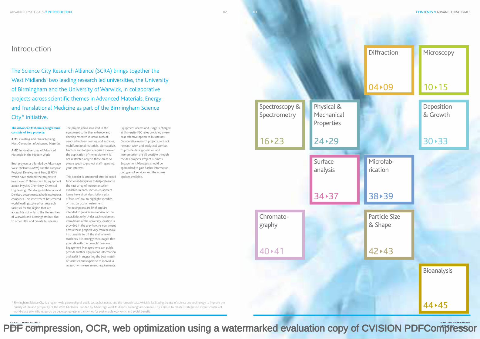
CONTENTS // ADVANCED MATERIALS 03
04 09
Diffraction
10 15
Microscopy
30 33
Deposition & Growth
24 29
Physical & Mechanical Properties
16 23
Spectroscopy & Spectrometry
40 41
Chromato- graphy
42 43
Particle Size & Shape
44 45
Bioanalysis
38 39
Microfab- rication
34 37
Surface analysis
ADVANCED MATERIALS // INTRODUCTION 02
The Advanced Materials programme
consists of two projects:
AM1: Creating and Characterising
Next Generation of Advanced Materials
AM2: Innovative Uses of Advanced
Materials in the Modern World
Both projects are funded by Advantage
West Midlands (AWM) and the European
Regional Development Fund (ERDF)
which have enabled the projects to
invest over £17M in scientific equipment
across Physics, Chemistry, Chemical
Engineering, Metallurgy & Materials and
Dentistry departments at both institutional
campuses. This investment has created
world leading state-of-art research
facilities for the region that are
accessible not only to the Universities
of Warwick and Birmingham but also
to other HEIs and private businesses.
The projects have invested in the
equipment to further enhance and
develop research in areas such of
nanotechnology, coating and surfaces,
multifunctional materials, biomaterials,
fracture and fatigue analysis. However
the application of the equipment is
not restricted only to these areas so
please speak to project staff regarding
your interests.
This booklet is structured into 10 broad
functional disciplines to help categorise
the vast array of instrumentation
available. In each section equipment
items have short descriptions plus
a ‘features’ box to highlight specifics
of that particular instrument.
The descriptions are brief and are
intended to provide an overview of the
capabilities only. Under each equipment
item details of the university location is
provided in the grey box. As equipment
across these projects vary from bespoke
instruments to off the shelf analysis
machines, it is strongly encouraged that
you talk with the projects’ Business
Engagement Managers who can guide
provide further equipment information
and assist in suggesting the best match
of facilities and expertise to individual
research or measurement requirements.
Equipment access and usage is charged
at University FEC rates providing a very
cost effective option to businesses.
Collaborative research projects, contract
research work and analytical services
to provide data generation and
interpretation are all possible through
the AM projects. Project Business
Engagement Managers should be
approached to gain further information
on types of services and the access
options available.
The Science City Research Alliance (SCRA) brings together the
West Midlands’ two leading research led universities, the University
of Birmingham and the University of Warwick, in collaborative
projects across scientific themes in Advanced Materials, Energy
and Translational Medicine as part of the Birmingham Science
City* initiative.
* Birmingham Science City is a region-wide partnership of public sector, businesses and the research base, which is facilitating the use of science and technology to improve the
quality of life and prosperity of the West Midlands. Funded by Advantage West Midlands, Birmingham Science City’s aim is to create strategies to exploit centres of
world-class scientific research, by developing relevant activities for sustainable economic and social benefit.
Introduction
PDF compression, OCR, web optimization using a watermarked evaluation copy of CVISION PDFCompressor

DIFFRACTION // ADVANCED MATERIALS 05
Bruker D8 Advance Diffractometer
Routine measurement of powder X-ray diffraction patterns for
identification of crystalline phases, purity estimation and/or
determination of crystal structure, measurement of powder
X-ray diffraction patterns up to 1100ºC in air.
High resolution powder X-ray Diffractometer operating in transmission mode
with automatic sample changer, monochromatic Cu radiation, LynxEye
position-sensitive detector.
Features
Location: Birmingham 1.1 & 1.2
Bruker D5000 & D5005 Diffractometer
D5000
Routine measurement of powder X-ray diffraction patterns of
samples in capillaries from 80 to 500K. This system will be of
most interest to those looking at organic samples such as
pharmaceuticals or air-sensitive species.
High resolution powder X-ray Diffractometer operating in capillary mode with low
temperature cryostream, monochromatic Cu radiation, Braun position-sensitive detector.
Powder X-ray Diffractometer operating in reflection mode using Cu or Mo radiation.
Features Features
Location: Birmingham 1.3 & 1.4
D5005
Routine measurement of medium resolution powder X-ray
diffraction patterns using Cu or Mo radiation.Diffraction
ADvANCED MATERIALS // DIFFRACTION
04 08
PDF compression, OCR, web optimization using a watermarked evaluation copy of CVISION PDFCompressor

DIFFRACTION // ADVANCED MATERIALS 07
Panalytical X’Pert Pro MRD
High resolution X-ray diffraction is an important technique
for studying individual Bragg peaks of single-crystal and
thin-film materials.
This machine is suitable for the study of single crystals, thin films (including
multilayers) and polycrystalline materials (e.g. ceramics). Typical materials include
semiconductors (SiGe, GaAs etc), Magnetic Multilayers, Ferroelectrics
(PZT, LiNbO3), Photovoltaic thin films and metallic rods / sheets.
The Panalytical X’Pert Pro MRD is a high resolution single crystal X-ray Diffractometer. In its
standard configuration, the MRD is equipped with a Cu Kα1 hybrid monochromator as the
incident beam optics and a receiving slit / analyser crystal as the diffracted beam optics.
This offers the best combination of counts to resolution for most routine applications.
The optics can be interchanged relatively quickly to tailor the Diffractometer to the
application required. For highest resolution measurements, a mirror & monochromator
combination can be used. For reflectivity measurements, a parallel plate collimator is
available on the diffracted beam optics enabling measurements out to larger angles than
possible with the standard optics.
Additionally, the optics can also be reequipped to allow stress and texture measurements to be
undertaken in point focus. The MRD is equipped with a PiXcel solid state detector enabling
better counting statistics, high linearity and eliminating the need for a beam attenuator.
An Anton Paar DHS900 domed hot stage, allowing non-ambient studies on thin-films and
ceramics at temperatures of up to 900ºC. Software is available for the analysis of rocking
curves, reflectivity, stress and texture measurements.
Features
Location: Warwick 1.28
Techniques available include:
Rocking curve analysis and reciprocal space mapping - Crystalline quality,
accurate lattice parameters, strain & misorientation.
Reflectometry and thin film phase analysis - Layer thickness & composition
Residual stress and texture analysis
Diffuse scatter measurements
In-plane and grazing incidence diffraction
Non-ambient diffraction - phase transitions, layer annealing studies.
ADVANCED MATERIALS // DIFFRACTION 06
Bruker S8 Tiger X-Ray Fluorescence (XRF) Spectrometer
This system is capable of determining the elemental composition of
samples, including solids, powders and liquids. It is able to detect
elements from oxygen through to uranium.
The system is not optimised for elements lighter than oxygen and therefore not
suitable for purely hydrocarbons or organics. Sample sizes can range from powders
below 1g, to solids with diameters of up to 3cm (flat surface required).
The measurement is non-destructive in most cases.
Wavelength Dispersive XRF system
Elemental analysis of materials, predominately inorganic solids
and powders
Optimised for detecting and quantifying elemental components ranging from
oxygen through to uranium at major, minor and trace (ppm) levels
Capable of handling small sample sizes (<1g)
Qualitative, fully quantitative and standardless analyses.
Features
Location: Birmingham 1.9
Oxford Diffraction Gemini R CCD Diffractometer
X-ray diffraction is an important tool for structural determination
of single crystals, both organic and inorganic. Usage spans from
routine structural work on organic and metal-organic small
molecules to highly detailed investigations of heavy metal oxides
that can include twins, modulated structures or diffuse scattering.
The Oxford Diffraction Gemini R CCD X-ray Diffractometer is a powerful tool for the
measurement of single crystals. The Gemini R is a Kappa geometry goniometer equipped
with dual wavelength (Cu/Mo) fine focus X-ray sources, graphite monochromators and
Enhance optics. The detector is a Ruby Charge Coupled Device area detector, which
allows for extremely fast data collection of the entire Ewald sphere. The Oxford
Diffraction CrysAlisPro software enables data collection, data integration and absorption
corrections to be performed, and is used in conjunction with refinement software such as
ShelX or Jana. For low temperature experiments (80K-400K) an Oxford Cryosystems
Cobra is attached to the system. Additionally, an optical stereomicroscope is used for
mounting and alignment of samples.
Features
Location: Warwick 1.30
PDF compression, OCR, web optimization using a watermarked evaluation copy of CVISION PDFCompressor
DIFFRACTION // ADVANCED MATERIALS 09ADVANCED MATERIALS // DIFFRACTION 08
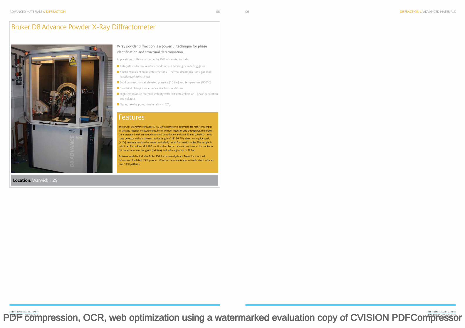
Bruker D8 Advance Powder X-Ray Diffractometer
The Bruker D8 Advance Powder X-ray Diffractometer is optimised for high-throughput
in-situ gas reaction measurements. For maximum intensity and throughput, the Bruker
D8 is equipped with unmonochromated Cu radiation and a Ni filtered vÅNTEC-1 solid
state detector with a maximum active length of 12° 2θ. This allows very quick static
(~10s) measurements to be made, particularly useful for kinetic studies. The sample is
held in an Anton Paar XRK 900 reaction chamber, a chemical reaction cell for studies in
the presence of reactive gases (oxidising and reducing) at up to 10 bar.
Software available includes Bruker EvA for data analysis and Topas for structural
refinement. The latest ICCD powder diffraction database is also available which includes
over 100K patterns.
Features
Location: Warwick 1.29
X-ray powder diffraction is a powerful technique for phase
identification and structural determination.
Applications of this environmental Diffractometer include:
Catalysts under real reactive conditions - Oxidising or reducing gases
Kinetic studies of solid state reactions - Thermal decompositions, gas solid
reactions, phase changes
Solid gas reactions at elevated pressure (10 bar) and temperature (900ºC)
Structural changes under redox reaction conditions
High temperature material stability with fast data collection - phase separation
and collapse
Gas uptake by porous materials - H, CO2.
PDF compression, OCR, web optimization using a watermarked evaluation copy of CVISION PDFCompressor

MICROSCOPY // ADVANCED MATERIALS 11
Confocal Microscope
Raman Microscope
Leica TCS SP5 X & Leica TCS SPE
Renishaw InVia Reflex and Witec Alpha 300R
Confocal microscopy may be used to investigate soft matter
surfaces and interfaces allowing observation of the interaction
of a wide range of molecules including polymers, colloids,
electrode (sensor) surfaces etc.
Allows ultra-fast imaging and the widest range of excitation wavelengths in the
visible range via a continuously tuneable laser.
Provides spatially resolved information on structure, bonding,
constituents, and electronic structure of a wide variety of
functional and structural materials.
Examples of applications of Raman microscopy include the differentiation of
polymorphs, chemical mapping in the pharmaceutical industry, detection and
monitoring of stress in silicon based microelectronics, and identification of high
temperature and pressure treated diamonds.
Tuneable super continuum laser source: 470 to 670nm in 1nm increments
Laser argon source with 5 selectable wavelengths from 458 to 514nm,
diode laser 405nm
Up to 8 simultaneous excitation wavelengths
5 detection channels
Configurable in upright and inverted configurations
Ultra fast bidirectional scan (max 16KHz).
325, 442, 514.5, 532, 633, 785nm lasers
CCD detector for visible to near-IR plus InGaAs for IR
Temperature: 77K - 873K
Automatic sample stage
Surface mapping 1μm spatial resolution
3D analysis of transport samples using confocal option.
Features
Features
Location: Warwick & Birmingham 2.6a & 2E33
Location: Warwick & Birmingham 2.5a, 1.5 & 2E20
Microscopy
ADvANCED MATERIALS // MICROSCOPY
10 15
PDF compression, OCR, web optimization using a watermarked evaluation copy of CVISION PDFCompressor

MICROSCOPY // ADVANCED MATERIALS 13
Low temp scanning tunnelling microscope (STM)
The key to STM is that it can image and probe individual atoms.
This allows electronic and vibrational spectroscopy with atomic-scale
spatial resolution. They can also image larger areas of surfaces
(~ 2 mm2) still with high spatial resolution.
Possible applications range from probing the fundamentals of surface induced
catalysis to arranging individual atoms in pre-designed structures, e.g., writing
words and letters using individual atoms.
Operational temperature range: from 4.6K to 300K (measured with Si-diode)
Conducting sample: metal, graphite and semiconductor
Sample size: 10mm x10mm (standard sample plates)
Scan range: 1.8x1.8μm2 @4.6K – 5.6x5.6μm2 @ 300K
Gap voltage: ±1 v and ±10 v (smallest increment 30μv and 300μv)
Tunnelling current: 1pA to 300nA with feedback loop active
Z-stability: <0.05 Å (rms)
Temperature range of manipulator: up to 1170K on heater stage; down to <100K on
cooling stage
Base pressure in ultra-high vacuum: 10-12~10-10 mbar
Measurement control software: NANONIS SPM Control System.
Features
Location: Birmingham 1.13
Ultra High vacuum Scanning Tunnelling MicroscopeScanwel
Atomic force microscope capable of imaging in air and fluid, as well as making electrical measurements. A wide range of samples may be studied such as nanoparticles, electrode surfaces, thin films and biological samples.
Samples can be prepared in-situ by noble gas ion sputtering and annealing and direct heating (i.e. for semiconductor wafers). Gas, organic and electron beam metal molecular beam epitaxy (MBE) sources are available.
STM can be used for structure determination of surfaces with molecular and atomic resolution and local electronic structure determination.
Base pressure 1 x 10¹⁰ mbar
Measurement temperatures liquid N2
and liquid He including cooled
sample manipulator
Maximum scan area 400nm2
Features
Location: Warwick 2.25
White Light Laser Source and Near Field Optical MicroscopePark high resolution AFM, Park Near Field Optical Microscope (NSOM), SC400 Fianium white laser source, Hammamatsu PMT, Andor CCD spectrometer, Tsunami laser.
The AFM permits to achieve morphological analysis of the samples with a
resolution less than 1Å. Confocal system permits to achieve 3D optical images of
the samples and to analyse their fluorescence properties. White laser source
provide broadband excitation of the samples.
SC400 from Fiannium: 2W femtosecond white-light laser source (80MHz repetition rate, 400fs pulses, available wavelengths: 400-1500nm)
XE-NSOM from Park Systems: Cantilever-based near-field optical scanning microscope both in transmission & reflection modes (can be used as well as a contact, tapping or non-contact AFM)
Nikon NE-2000 inverted microscope, used in conjunction with the NSOM for transmission mode
Andor water-cooled CCD spectrometer.
Features
Location: Birmingham 1.16
ADVANCED MATERIALS // MICROSCOPY 12
Atomic Force Microscope (AFM)NanoWizard & Veeco diMultimode V
Atomic force microscope capable of imaging in air and fluid as well
as making electrical measurements. Large scale samples may be
studied such as nanopartilces, electrode surfaces, thin films and
biological samples.
Measurements at variable temperatures with perfusion possibilities. Applications include 3D surface topography and adhesion force mapping.
Large scan field of 100 × 100 × 15μm3
Range (x, y, z): 100μm, 100μm, 100μm
Sub Ångstrom resolution
Dedicated conducting module
Comprehensive range of accessories:
Cellhesion controller
Biocell controller
Petri-dish Heater
Electrochemical cell
Biopotentiostat.
Features
Location: Warwick & Birmingham 2E29 & 2.8
JEOL Aberration-corrected Transmission Electron Microscope (JEM-2100F)
High resolution imaging, Materials qualification, Chemical
analysis, Particles detection/characterisation, Defects analysis,
Microstructural characterisation.
The JEM-2100F is a JEOL field emission gun transmission electron microscope with an:
Ultra-high-resolution pole piece
Operates at 200kv
It can work in TEM mode with a point resolution of 0.19 angstrom and STEM mode
with a corrected probe size of 1 angstrom.
EELS energy resolution can get to 0.95 ev for standard beam emission.
Features
Location: Birmingham 1.2
PDF compression, OCR, web optimization using a watermarked evaluation copy of CVISION PDFCompressor

MICROSCOPY // ADVANCED MATERIALS 15ADVANCED MATERIALS // MICROSCOPY 14
GATAN ORIUS® CCD GATAN ORIUS® CCD camera - large format (11 Megapixel) retractable and fiber-optical coupled CCD
viewing and recording images and electron diffraction patterns. The high speed viewing mode also allows the user to replace the traditional TEM viewing screen. Operations such as microscope alignments, stigmation, and focus can be performed with high precision using the camera display instead of the TEM viewing screen.
The SC1000 offers a high speed (>14 fps - frames per second) image viewing mode. This allows the user to search areas within the sample quickly and efficiently.Another benefit of the high frame rate of the SC1000 is the capability of TEM in-situ observations. The SC1000 can output high quality (dark and gain corrected) LIvE images via a digital video stream.
Features
Location: Warwick 1.31
Cathodoluminescence SystemGatan MonoCL3 with Digiscan
The Cathodoluminescence system is attached to a scanning electron microscope (SEM) and may be used to investigate chemical composition including trace elements, electronic structure, and studying stress information in semiconductors and insulators. The system may also be used for mineral analysis.
Spectra can be measured in parallel with scanning
electron microscopy
Monochromatic and panchromatic imaging modes
Wavelength range 185 - 850nm.
Features
Location: Warwick 2.5b
High Speed Camera with MicroscopeLeica DM 2500M with Vision Research Phantom Monochrome v.7.3
High speed camera system may be used to study microscale dynamic processes.
Up to 6688 frames per second at
800 x 600 resolution
8, 10, 12 or 14 bit image depth
Continuously adjustable shutter speeds down
to 1 μs.
Features
Location: Warwick 2.6b
GATAN PIPS™ Ion miller
For the thinning of samples such as silicon, ceramics, glass ceramics etc for viewing in the Transmission Electron Microscope.
The PIPS is a user-friendly precision ion polisher
designed to produce high quality, TEM specimens
with minimal effort. The muiller has a Liquid Nitrogen
cooled specimen stage and CCD zoom camera to
view milling progress.
Features
Location: Warwick 1.33
Zeiss Axioimager and Stemi2000 stereo microscopesOptical Microscopy
Axio Imager from Carl Zeiss, designed for quality control, quality assurance, materials analysis, and for the development of new materials. Ideal for routine applications and research. Darkfield illumination reveals unevenesses in the surface (such as phase boundaries between graphite and matrix or break-outs). C-DIC (color contrast): The matrix is contrasted because of the relief. Hard and soft grain components as well as polishing inconsistencies (exclusively mechanically polished) are visible.
Microscope can offer:
50 - 1000 times magnification
Reflective/Transmitted light source
Bright field imaging
Dark field imaging
Differential Interference Contrast imaging
3.2 megapixel camera.
Features
Location: Warwick 1.32
PDF compression, OCR, web optimization using a watermarked evaluation copy of CVISION PDFCompressor

Scanning Probe Energy Loss Spectrometer (SPELS)Scanning Probe Energy Loss Spectrometer (SPELS) Instrument Development
This laboratory facility focuses on the design and development of
new analytical instrumentation and techniques.
A present example being the SPELS; an instrument patented by the University of
Birmingham (UK patent No. 0002367.1). A previous example of an instrument
developed is the novel “time-of-flight” mass filter that is used to separate small
particles of different sizes generated from a material source (metal or semiconductor).
The mass filter is also patented in the UK and internationally.
Our extensive experience with instrumentation development allows us to provide
services and consultancy.
Sample Size: 10mm x 10mm x 1mm
Maximum scan range: 3um x 3um x 1.5um (height)
Primary Beam energy range: 0-250 ev
Energy resolution: 300mev
Spatial resolution: sub um
Room temperature only; Conducting samples only; Ultra high vacuum only;
Surface sensitive.
Features
Location: Birmingham 1.1
SPECTROSCOPY & SPECTROMETRY // ADVANCED MATERIALS 17
High Resolution Hybrid Mass Spectrometer Coupled with UHPLCBruker MaXis with Proxeon Easy-nLC and Dionex RS3000 HPLC & Bruker HCT-Ultra, ETD Discovery with Agilent 1200 UHPLC
Ultra high resolution – time of flight mass spectrometer (TOF-MS)
for use in applications such as: identification of small molecules,
metabolomics quantitative proteomics, biomarker discovery,
characterisation of (bio)polymers and supramolecular assemblies.
Ion trap MS:
CID/ETD
MSn
LC-MS/MSn
MaXis MS:
Resolution > 40,000 FWHM
MS and MS/MS mass accuracy typically between 600 - 800 ppb
Acquisition rate up to 20Hz
Features
Location: Warwick 2.4
SpectroscopySpectro metry
ADvANCED MATERIALS // SPECTROSCOPY & SPECTROMETRY
16 23
&
PDF compression, OCR, web optimization using a watermarked evaluation copy of CVISION PDFCompressor

SPECTROSCOPY & SPECTROMETRY // ADVANCED MATERIALS 19
Multi Frequency FT Electron Paramagnetic Resonance (EPR) Spectrometer
A large number of materials have unpaired electrons. These include
free radicals, many transition metal ions, and defects in materials.
Free electrons are often short-lived, but still play crucial roles in
many processes such as photosynthesis, oxidation, catalysis, and
polymerisation reactions. Hence EPR applications span a wide
range of areas from quality control to molecular research in fields
such as material research, structural biology, and quantum physics.
For example EPR is able to provide information on long-range interactions (1 to 8nm) between paramagnetic centres and extract conformational information which are difficult to obtain by other technologies (such as NMR, X-ray crystallography).
This is a highly versatile multi-frequency (9.5 and 34 GHz) Fourier Transform Electron Paramagnetic Resonance (EPR) spectrometer equipped for all FT-EPR and Electron Spin Echo techniques including ESEEM and 2D-HYSCORE to measure spin density distribution and distances through the hyperfine interaction between electron and nuclear spins, SECSY and EXSY to measure correlations and exchange rates, Pulse-ELDOR and DEER to measure long range distances by electron-electron spin dipolar coupling, pulse-ENDOR to measure hyperfine interactions and nuclear spin relaxation, and laser triggered experiments to investigate chemical reactions and triplet states.
Features
Location: Warwick 1.35
High Resolution Electron Energy Loss (HREELS) SpectrometerLK ELS5000MCA
The HREELS technique allows one to resolve finely spaced energy
features, necessary for analysing molecular vibrations. The
advantage of HREELS over other energy loss spectroscopy is that
momentum can be transferred by the electrons to the features
being measured, this gives the experimentalist extra information
regarding the energy-dispersion relations of surface features and
the ability to excite indirect transitions (where spectroscopy with
photons as the probe is limited to direct transitions).
Energy Resolution (Direct Beam) = 0.5mev
Beam Energy = 1ev to 70ev
Sample size = up to 2cm square attached to omicron plate
Temperature range = 77K to 800K (potentially from 4K with He)
Energy range = 0 to 2ev window, with 40ev movement range
Pressure = 10E-10torr (UHv), Prep = Ar Ion
sputtering, E-beam annealing, LEED analysis.
Features
Location: Birmingham 1.18
ADVANCED MATERIALS // SPECTROSCOPY & SPECTROMETRY 18
Mass Spectrometry System for Surface AnalysisKORE Surface Seer
Time-of-flight secondary ion mass spectrometer (TOF-SIMS)
instrument for characterisation of surfaces, detection of all elements
as well as identification of organic species and thin film profiling.
Examples of use include the study of self-assembled monolayers.
Positive and negative SIMS with reflectron analyser
Mass range >1000m/z.
Features
Location: Birmingham 2E5
MALDI Mass SpectrometerWaters Micro MX
High-performance, matrix-assisted laser desorption/ionisation time-of-flight
mass spectrometer featuring parallel position sensitive detection (PSD)
technology for confirming protein identification and determining post-
translational modifications.
Negative ion capability allows applications in genotyping and polysaccharide analysis.
Enables analysis of sub-femtomole quantities
of biological and synthetic molecules
Molecular weight range 200 Da - >500 KDa
In reflection mode with m/z <4kDa high
resolution spectra obtained.
Features
Location: Birmingham 2E2
Gas Chromotagraphy Mass Spectrometer (GCMS)Waters GCT Premier
An orthogonal acceleration time-of-flight mass spectrometer with high
resolution for the selectivity needed to separate analyte spectra from isobaric
interferences and background chemical noise. Identifies the elemental
compositions of small molecules.
Sub-5 ppm RMS
EI, CI and FI ionisation.
Features
Location: Birmingham 2E3
PDF compression, OCR, web optimization using a watermarked evaluation copy of CVISION PDFCompressor

SPECTROSCOPY & SPECTROMETRY // ADVANCED MATERIALS 21
Lambda 1050 Spectrophotometer for Optical Absorption
Architectural and Specialty Glass: Energy conservation is more important now
than ever before. Analysis of coated glass provides important information on
thermal efficiency and other key design considerations.
Solar Energy Research: The LAMBDA 1050’s capability in the NIR region allows full
characterisation of not only the active solar cell materials but also the reflective
protective covering.
The LAMBDA 1050 is a high sensitivity and high
resolution spectrophotometer for a wide range of
demanding applications, such as high absorbing glass,
optical coatings or thin film filters over the wavelength
range 190 - 3300nm. It also features two large
sampling compartments and polarizing optics.
It is equipped with an Oxford Instruments Optistat
cryostat enabling measurements in the range 3.7
to 300K.
Features
Location: Warwick 1.34
This instrument combines several electron spectroscopy techniques that can be applied to investigate the chemical composition and electronic structure of surfaces and interfaces. The instrument includes a monochromated twin-anode X-ray source (Al & Mg K
a) and a multi-channel channel concentric
hemispherical analyser for high resolution X-ray photoelectron spectroscopy (XPS - supplied by Omicron GmbH).
In addition there is a high intensity un-monochromated X-ray source, a low energy electron flood gun (for non-conducting samples), low energy electron diffraction (LEED) for surface crystallography, an ion sputter gun for elemental depth profiling, and a preparation chamber for deposition and in-situ sample pre-treatment. Samples are transferred through the system on sample plates and can be moved to an adjoining chamber with high resolution Uv photoelectron spectroscopy (UPS - supplied by vG-Scienta) consisting of a monochromated high intensity helium discharge lamp and a Scienta R4000 high resolution electron analyser. This combination allows valance band electronic structure of materials and deposited overlayers to be investigated, with samples mounted on a 5-axis manipulator with a temperature range of 30 -1000K.
X-ray and Uv Photoelectron Spectroscopy (XPS & UPS)Omicron Gmbh & VG Scienta
High resolution XPS for surface and interface chemical analysis
Facilities for electron spectroscopy of non-conducting samples
Electronic structure determination, valance band and Fermi surface mapping
Elemental depth profiling
vacuum suitcase transfer from other growth/vacuum chambers under UHv conditions.
Features
Location: Warwick 1.22
Steady State and Time Correlated Single Photon Counting (TCSPC) Fluorescence SpectrometerEdinburgh Instruments
Modular instrument for measuring fluorescence and phosphorescence decays on
molecular nanomaterials.
Time range 100ps - 10s
Xe flashlamp, pulsed diode laser and LED
Detection in visible and near IR.
Features
Location: Birmingham 2E10
ADVANCED MATERIALS // SPECTROSCOPY & SPECTROMETRY 20
Solid State NMR suiteMillburn House has thirteen superconducting magnets for
performing NMR, ranging from 850 MHz (proton Larmor frequency)
to 100 MHz for solid-state NMR, 700 and 600 MHz for solution-
state NMR and a three magnet solid-state DNP system.
Over sixty probes enable NMR to be performed over a wide temperature range from
90 K to 1000 K, with air or nitrogen gas, and MAS rotors ranging from 1.3 mm
(65 kHz spinning) - 1.8 mm (45 kHz spinning) - 2.5 mm (35 kHz spinning) - 3.2 mm
- 4 mm - 7 mm - 9 mm - 14 mm (4 kHz spinning). There are also two
Double-Rotation (DOR) probes.
600 MHz Bruker Avance II+
500 MHz Bruker Avance III
400 MHz Bruker Avance 400
300 MHz varian InfinityPlus
300 MHz Field-Sweep
Chemagnetics Infinity
200 MHz Chemagnetics Infinity
100 MHz Chemagnetics Infinity
DNP: 143 MHz Super Widebore
Chemagnetics Infinity
DNP: 600 MHz Sweepable varian
Bruker 2.5 mm
Bruker 3.2 mm
Bruker 4 mm
Bruker 7 mm
Chemagnetics/varian 3.2 mm
Chemagnetics/varian 4 mm
Chemagnetics/varian 6 mm
Chemagnetics/varian 9.5 mm
Chemagnetics/varian 14 mm
Doty 4 mm
Doty 7 mm
Samoson 1.8 mm
Samoson DOR
Spectrometers Rotors
Location: Warwick 1.36
850MHz Solid State NMRBruker 4 channel HFXY with 11 MAS and static probes
The 850 MHz system is a world-leading UK facility delivering
advances in materials science, chemistry, biology, earth science and
physics, jointly funded through EPSRC, BBSRC and the Advanced
Materials (1 and 2) projects.
Solid-state NMR provides information about the structure of solids and is especially
suitable for studying disordered materials which lack long range order.
Solid-state NMR uses nuclear spin as a “local probe” to investigate short range
arrangements in materials in contrast to, for example, X-ray diffraction. It can be also
used to study the structure and conformations of single molecules, the interaction
between various molecules and nuclei, local dynamics, kinetics and dynamics at
molecular levels. The systems of interest can range from small organic or inorganic
molecules, to mid-sized clusters or peptides and up to large structures such as proteins
or polymers.
UltraShield cryomagnet: bore size 89mm and persistent magnetic field of 20 Tesla
Avance III ultrafast console (4 channels)
Temperature control down to 150 K
A range of 1.3, 2.5, 3.2, 4 and 7 mm MAS probes
Features
Location: Warwick 1.38
PDF compression, OCR, web optimization using a watermarked evaluation copy of CVISION PDFCompressor

SPECTROSCOPY & SPECTROMETRY // ADVANCED MATERIALS 23ADVANCED MATERIALS // SPECTROSCOPY & SPECTROMETRY 22
Near IR Spectrometer Varian Cary 5000 Near IR Spectrometer with Harrick Praying Mantis Diffuse Reflection Accessory
Near Infra-Red Spectrometer with cryogenic unit for liquid nitrogen temperature measurements Praying mantis
accessory allows reliable diffuse reflectance studies of powders and other rough surface solid samples.
Wavelength: 175 – 3300 nm
Cryogenic temperatures
Solutions, solid samples and thin films.
Features
Location: Birmingham 2E9
300 and 400 MHz Solution NMR SpectrometersBruker BioSpin Avance III 300 & 400
300 and 400 MHz NMR Spectrometers refurbished and equipped with automation and new Avance III controllers for routine
solution NMR analysis. High performance digital NMR for characterisation of molecular materials and nanoparticles.
1H, 13C, 19F, 31P as well as more demanding
multi-pulse experiments
Temperature range -95°C to +110°C
Capacity to study traditional inorganic nuclei.
Features
Location: Birmingham 2E1
varian 660 IR FTIR Spectrometer with Pike MIRacle diamond ATRRecords vibrational spectra. Capable of providing information on the chemical constitution of samples and the nature of bonds present. Records infrared spectra
Optimised for powder samples
Environmental chamber for the measurement of
air sensitive samples.
Features
Location: Birmingham 1.7
PDF compression, OCR, web optimization using a watermarked evaluation copy of CVISION PDFCompressor
25 PHYSICAL & MECHANICAL PROPERTIES // ADVANCED MATERIALS
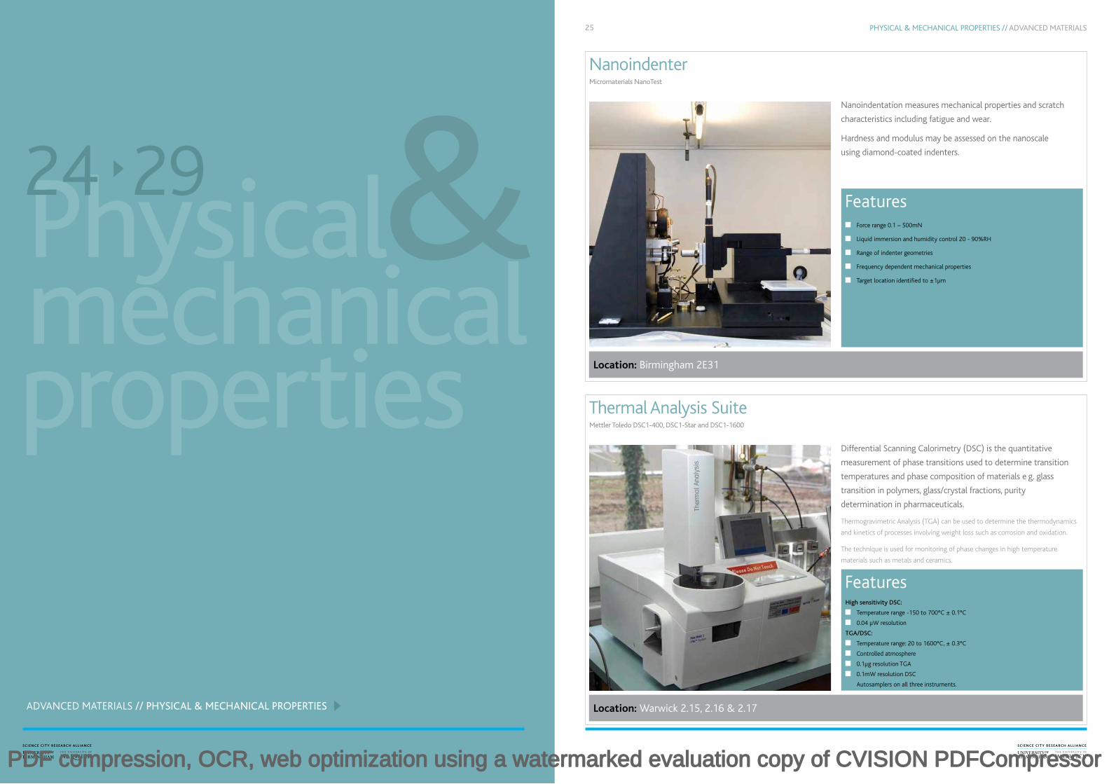
Nanoindenter
Thermal Analysis Suite
Micromaterials NanoTest
Mettler Toledo DSC1-400, DSC1-Star and DSC1-1600
Nanoindentation measures mechanical properties and scratch
characteristics including fatigue and wear.
Hardness and modulus may be assessed on the nanoscale
using diamond-coated indenters.
Differential Scanning Calorimetry (DSC) is the quantitative
measurement of phase transitions used to determine transition
temperatures and phase composition of materials e g. glass
transition in polymers, glass/crystal fractions, purity
determination in pharmaceuticals.
Thermogravimetric Analysis (TGA) can be used to determine the thermodynamics
and kinetics of processes involving weight loss such as corrosion and oxidation.
The technique is used for monitoring of phase changes in high temperature
materials such as metals and ceramics.
Force range 0.1 – 500mN
Liquid immersion and humidity control 20 - 90%RH
Range of indenter geometries
Frequency dependent mechanical properties
Target location identified to ±1μm
High sensitivity DSC:
Temperature range -150 to 700°C ± 0.1°C
0.04 μW resolution
TGA/DSC:
Temperature range: 20 to 1600°C, ± 0.3°C
Controlled atmosphere
0.1μg resolution TGA
0.1mW resolution DSC
Autosamplers on all three instruments.
Features
Features
Location: Birmingham 2E31
Location: Warwick 2.15, 2.16 & 2.17
Physical mechanical
ADvANCED MATERIALS // PHYSICAL & MECHANICAL PROPERTIES
24 29
properties
&
PDF compression, OCR, web optimization using a watermarked evaluation copy of CVISION PDFCompressor
PHYSICAL & MECHANICAL PROPERTIES // ADVANCED MATERIALS 27
Dynamic vapour Sorption (DvS) Moisture Adsorption ApparatusSurface Measurement Systems DVSA-STD
The sorption apparatus characterises the behaviour of materials in different
humidity and temperature environments.
vapour sorption isotherms can be measured and compound stability evaluated.
Additionally, surface adsorption effects can be examined.
Gravimetric measurements using 0.05μg
resolution microbalance
Organic solute and water reservoirs
Temperature range 5 to 60°C
Analysis of solid and powder samples.
Features
Location: Birmingham 2E19
CalorimeterTA Instruments TAM III
Calorimetry can be used for ultra-sensitive heat flow measurement.
The equipment can monitor chemical stability, physical degradation and
polymorphic transformations.
Example applications include polymer and pharmaceutical development, cement
formulation and accelerated corrosion testing.
Up to four independent calorimeters can be
used simultaneously
2 x microcalorimeters, 1 x multicalorimeter,
1 x solution calorimeter
Isothermal, step-isothermal or temperature
scanning modes
15 - 150°C temperature range
Isothermal and slow scanning (2°C h 1)
Temperature stability < 0.01mK / 24h.
Features
Location: Warwick 2.18
Dissolution Apparatus Varian 705-DS
Monitors the degradation of resorbable biomaterials in addition to release from
pharmaceutical materials and devices. Applications include formulations,
materials, soluble dosage forms and release in vivo.
8-vessel / 8-spindle configuration
Standard 1L vessels
US Pharmacopeia (USP) compliance.
Features
Location: Birmingham 2E21
Helium PycnometerMicro-meritics Accupyc II 1340
High-speed, high-precision volume measurements and density calculations on a
wide variety of powders, solids, and slurries as well as bulk objects and porous
scaffolds. Uses gas displacement to measure volume.
Measures the absolute density of solids and
slurries with volumes 0.01 to 1.0cm3.
Features
Location: Birmingham 2E22
ADVANCED MATERIALS // PHYSICAL & MECHANICAL PROPERTIES 26
Netzsch STA 449 F1 Jupiter thermal analyser
The thermal analyser can provide a variety information including:
Temperature and composition of evolved gases
Mass change for analysis, eg of oxygen content in materials
Information on phases changes (DSC) even when no mass change occurs.
The Netzsch analyser allows thermal analysis
of materials up to temperatures of 1400°C in
controlled atmospheres. Mass change and
calorimetric effects can be monitored
simultaneously. The equipment is linked to a
mass spectrometer which allows immediate
analysis of evolved gases.
Features
Location: Birmingham 1.6
RheometerTA Instruments AR G2
Rheological analysis of liquids and soft solids for use in implants
and delivery systems.
Assessment of the material properties using cone and plate,
concentric cylinder and vane geometries is possible.
Ultra-low nano torque control down to 3nN m
in controlled stress and direct strain
controlled modes
Frequency range 10 6 - 100Hz
Temperature control up to 200°C
Measurement of Newtonian and
non-Newtonian materials.
Features
Location: Birmingham 2E34
MUARC (Midlands Ultracold Atom Research Centre)
Study the underlying physics of novel materials or of quantum
phenomena underlying material properties by the creation of well
defined artificial materials. Examples would be the creation of
artificial superconductors, magnetically frustrated systems or
conductors with well defined impurities or disorder causing
resistivity or localisation.
Provide a suitable laboratory environment to enable cold atom experiments aiming at
the creation of artificial materials. The facility will enable the creation and study of
artificial 2D materials with many degrees of freedom in parameters, e.g. tunnelling,
interaction, lattice geometry.
Features
Location: Birmingham 1.20
PDF compression, OCR, web optimization using a watermarked evaluation copy of CVISION PDFCompressor

Tribometry SuiteTribometer and Nanotribometer
Tribological measurements of friction, lubrication and wear. Nanotribometry may be carried out under controlled
humidity and temperature
Reciprocating motion and rotating motion.
Tribometer loads > 1N and Nanotribometer loads
1mN - 1N
variable environmental conditions.
Features
Location: Birmingham 2E26 & 2E27
Micro-Manipulation SystemCustom-built
Mechanical characterisation of single micro-particles, single cells, soft solids, MEMS devices, particle-particle interactions
and particle-surface interactions.
Measures:
Compression behaviour
Stress relaxation behaviour
Frequency-dependent behaviour
variable environmental conditions can
be employed.
Features
Location: Birmingham 2E30
PHYSICAL & MECHANICAL PROPERTIES // ADVANCED MATERIALS 29
Dental Wear SimulatorsProto-Tech Fatigue Cycler, Thermal Cycler and Shrinkage Stress Analyser
A: Thermal Cycler - reproduces the temperature cycling which occurs in the mouth to evaluate dental materials.
B: Polymerisation Stress Tester - measures stress and shrinkage in polymerisation of dental composites.
Thermal cycling: 0 – 80ºC
Fatigue testing:
Loading up to 400 N
Up to 4 parallel samples.
Features
Location: Birmingham 2E37
Micropore AnalyserMicromeritics ASAP2000 and Autopore IV
Determines the pore size distribution and pore volume of materials, including
dental and medical materials, porous scaffolds and catalysts. Example materials
include: catalysts and bio-scaffolds and gas storage materials such as carbons,
zeolites and metal organic frameworks.
Chemisorption can be used to investigate active metal dispersions or surface
acidity of catalysts. Materials with low surface areas such as powdered metals,
glass fibers, and natural organic materials can also be analysed.
Measures surface areas from 0.001 to 3000m2 g 1
Pore diameters from 0.003 to 360μm
Resolution > 0.1μL pore size.
Features
Location: Warwick 2.24 & 2E23
ADVANCED MATERIALS // PHYSICAL & MECHANICAL PROPERTIES 28
Quantum Design Physical Properties Measurement System (PPMS)
The Quantum Design PPMS is an open architecture, variable temperature-field
system, designed to perform a variety of automated measurements. It offers a
wide range of magnetic, thermal and electrical measurements.
Heat capacity: T range, 0.4K - 400K in magnetic
fields of up to 9T. Sample mass 5-500 mg with a
resolution of 10nJ/K @ 2.0K.
Transport Measurements: AC Resistivity, Hall
Effect, I-v Curve Tracing, and Critical Current
measurements, 1 nv sensitivity, nΩ resolution at 2 A,
drive amplitude 10μA to 2 A. Thermal conductivity,
dynamic range 0.1 to 250 W/mK, Seebeck coefficient,
range 1μv/K to 1v/K. For all the transport
measurements T range 1.8K - 400K in magnetic
fields of up to 9T.
Features
Location: Warwick 1.25
MPMS SQUID magnetometer
Magnetic Property Measurement System (MPMS) magnetometer utilises
Superconducting Quantum Interference Device (SQUID) technology.
The MPMS provides solutions for a unique class of sensitive magnetic
measurements in key areas such as high-temperature superconductivity,
biochemistry, and magnetic recording media.
Magnetisation Measurements: T range,
0.5K - 800K in magnetic fields of up to 7 T.
Maximum sample size ~9 mm diameter by ~20mm
long. DC magnetisation, sensitivity 1 x 10⁻⁸ emu
@ 0.25T.
AC susceptibility measurements: 0.1Hz to 1KHz,
sensitivity 2 x 10⁻⁸ emu at 0T.
Features
Location: Birmingham 1.26
Universal Mechanical TesterZwick/Roell Z030
Testing system for compressive and tensile strength of materials.
Example applications include tensile testing of polymers and compressive
testing of biocements. Powder compaction studies may also be undertaken.
Force range 10 mN to 30 kN
Liquid immersion facilities to work under
physiological conditions
Compressive, tensile and flexural testing.
Features
Location: Birmingham 2E24
Environmental Mechanical AnalyserInstron MicroTest 5848
Enables measurement of mechanical properties, such as tensile and compressive
strengths, as a function of humidity and temperature.
Fatigue studies may be conducted over expended time periods (weeks).
Force range 10 mN to 2 kN
Electromechanical position control ~ 5μm
Custom waveforms and strain patterns
Humidity range 10 - 80%RH
Temperature up- to 40°C.
Features
Location: Birmingham 2E25
PDF compression, OCR, web optimization using a watermarked evaluation copy of CVISION PDFCompressor

DEPOSITION & GROWTH // ADVANCED MATERIALS 31
Size Selected Cluster Beam
Pulsed Laser Deposition (PLD)
Small particles of very well defined sizes have many potential
applications, with many of them being explored at the moment in
the scientific community.
From an industrial perspective, one application is that of catalysis. The properties of
small particles (including chemical reactivity) are very different to their bulk
counterparts. Such particles could lead to a catalyst (either for the automotive
industry or for bulk chemical production) that is produced from much less material
in total.
This instrument consists of an ultra-high vacuum (UHv) pulsed
laser deposition (PLD) system with a series of in-situ surface
structural and chemical probes.
The PLD system (supplied by TSST B.v. Holland) allows target materials placed in the chamber to be ablated using a pulsed ultra-violet laser for the growth of thin films of materials - some only a few atoms thick - in a controlled manner. This is achieved by in-situ monitoring of the growth process using reflected high energy electron diffraction (RHEED) to ensure high crystalline perfection in a range of different materials. This PLD system allows different combinations of materials and interfaces to be fabricated from complex oxides to semiconductor materials. The use of UHv and high purity materials ensures that stoichiometric thin films of the highest structural quality can be grown. The system incorporates a number of in-situ surface diagnostic techniques such as X-ray photoelectron spectroscopy (XPS) for determining the surface composition, and scanning probe microscopy, (both STM and AFM - supplied by Omicron GmbH) for topographic and atomic resolution studies of surface and interface structure in the epitaxially grown materials.
Source type: magnetron sputtering
Target: Material: Most metals and selected semiconductors; Size: 2 inch OD, 6mm
thickness (direct cooling) or 4 mm thickness (indirect cooling)
Beam potential: -1.0kv to +1.0kv
Mass range: 30 amu to > 20,000,000amu
Mass resolution: up to 130 (m/∆m)
Transmission: up to 44%
Substrate voltage: -1.5kv to +1.5kv
Beam current : up to 3nA.
Controlled growth of high quality epitaxial thin films of complex oxides
Layer by layer, controlled deposition of the thin films of various materials
Deposition and growth of interfaces, multilayer and superlattice structures
Optimisation of the growth conditions by in-situ diagnosis of the as grown thin films by RHEED and XPS
Surface structure analysis in-situ using combined STM and AFM.
Features
Features
Location: Birmingham 1.10
Location: Warwick 1.21
Deposition growth
ADvANCED MATERIALS // DEPOSITION & GROWTH
30 33 &
PDF compression, OCR, web optimization using a watermarked evaluation copy of CVISION PDFCompressor

DEPOSITION & GROWTH // ADVANCED MATERIALS 33DEPOSITION & GROWTH // ADVANCED MATERIALS 32
Single Crystal Growth Machine(Cyberstar)
This equipment will be used to melt binary and ternary intermetallic
compounds in polycrystalline form. Rods of these compounds can
also be made using this method in preparation for crystal growth
by the floating zone technique.
This system will be used as a crystal growth system using 4 arcs (tetra arc) to melt
materials on a copper hearth
This system can be used to produce crystals of intermetallic materials -
alloys and compounds.
Includes a radio frequency power generator, capable of delivering 40kW has been
acquired to be used in conjunction with an existing cold boat system.
Features
Location: Warwick 1.23 & 1.24
Organic Thin Film Deposition and Solar Simulator SystemmBraun 200B Glovebox with Solar Simulator
The system may be used for the formation of thin organic films via evaporation and deposition with controlled rate and thickness.
Solar simulation allows the testing of the response of films to 1sun simulated solar irradiance.
Glovebox with two anti-chambers and evaporator
Solar Simulator with Xe Arc lamp (550W)
Quartz Crystal Microbalance for measurement
of film formation.
Features
Location: Warwick 2.4
Metal Evaporator Edwards E306 Coater
Purpose built clean room facility housing a variety of equipment to facilitate photolithographic processing of device structures.
Deposition is monitored by quartz
crystal microbalance
Deposition rates 0.01 or 0.001nm s 1
Features
Location: Birmingham 2E13
Photolithography Clean Room SuiteMoorfields electron beam evaporator, Recently upgraded Moorfields MiniBox thermal evaporator and sputtering system and Suss Microtec MJB4 Mask Aligner
Features
Location: Warwick 1.27
Moorfields electron beam evaporator - controlled
thin film deposition of metals such as Pt, Ni etc
Thermal evaporator and sputtering system
- controlled thin film deposition of both metals
and insulators including Pt, Au, Ti, Cr, Al, SiOx etc
Suss Microtec MJB4 Mask Aligner - high resolution
printing down to 0.5μm.
PDF compression, OCR, web optimization using a watermarked evaluation copy of CVISION PDFCompressor

SURFACE ANALYSIS // ADVANCED MATERIALS 35
Quartz Crystal Microbalance (QCM)
Ellipsometer
Qsense QCM-D E1 & E4 System
Nanofilm EP3-SE
The Quartz Crystal Microbalance provides mass and structural information on molecular layers that form on the surface of a sensor. Molecular adsorption and interactions can be monitored in real time under a variety of conditions. Sensors can be chemically modified to produce a range of surfaces for study.
QCM can be used in a range of applications, for example to investigate the
hydration of polymer films, monitor protein interactions with a variety of
surfaces, or study the effectiveness of surfactants in removing lipid films.
Ellipsometry may be used for the determination of film thickness,
morphology, microtribology, electric and optic properties of
multilayer metal/metaloxides; self assembled molecules and
thin film polymeric materials; next generation energy-efficient
glazings. Surface plasmon resonance package is available for
molecular surface interaction investigations.
Multiple sensor unit for up to four flow cells
in series or parallel configuration
Electrochemical cell
Temperature range from 15 - 45°C
Dissipation monitoring gives information on rigidity of film
Sensitivity of the order of 2ng cm-2
Resolution of 200 data points per second.
Spectroscopic ellipsometer with 46 wavelengths between 365nm to 1000nm
Wavelength and angle of incidence scanning
Mapping function
Lateral resolution 1μm
Surface plasmon resonance (SPR) cell.
Features
Features
Location: Warwick 2.3
Location: Warwick 2.10
SurfaceAnalysis
ADvANCED MATERIALS // SURFACE ANALYSIS
34 37
PDF compression, OCR, web optimization using a watermarked evaluation copy of CVISION PDFCompressor

SURFACE ANALYSIS // ADVANCED MATERIALS 37ADVANCED MATERIALS // SURFACE ANALYSIS 36
InterferometerKLA Tencor MicroXAM2
Interferometry measures surface topography and wear volume through
three-dimensional surface profiling.
Equipment may be used to measure coating film thickness up to 60μm.
vertical range up to 50mm
100mm x 100mm sample positioning stage
Phase mode for nanoscale resolution
Surface roughness may be quantified
Dissimilar materials analysis
Features
Location: Birmingham 2E28
Ti:Sapphire Femtosecond laser system. Optical measurements and characterisation
The system may be used for the formation of thin organic films via evaporation and
deposition with controlled rate and thickness. Measurements of materials reflectivity
and absorption properties, determination of excitation decay dynamics, determination
of real and imaginary parts of dielectric constants by means of static and time resolved
ellipsometry, design and implementation of advanced optical set-ups, optical
measurements automation and optimisation.
Micra ‘seed’ laser: 400mW pulses at 80MHz,
Lamda = 800nm, Pulse Duration 40fs,
Bandwidth 100nm.
Legend Amplifier: 4W pulses at 1kHz repetition,
Lambda = 800nm, Pulse Duration 30fs,
Bandwidth 40nm.
OPA for wavelength tuning between
250-20000nm.
CEP for <1mrad stability in phase of pulses.
Features
Location: Birmingham 1.17
Drop Shape AnalyserKruss DSA-100
Static and dynamic contact angles of liquids on surfaces, interfacial and surface
tensions of liquids and surface energies of solids can be measured. Applications
include wetting properties of plastics, glasses or metals, effectiveness of
surfactant solutions and investigating adhesion properties.
Contact angle (sessile drop)
Surface tension (pendant drop)
Tilting table
EDM/ODM module (Expanding Drop Method/
Oscillating Drop Method)
Humidity chamber
High speed camera available.
Features
Location: Warwick 2.19
PDF compression, OCR, web optimization using a watermarked evaluation copy of CVISION PDFCompressor

MICROFABRICATION // ADVANCED MATERIALS39
FEI Quanta 3D Focussed Ion Beam - Scanning Electron Microscope (FIB-SEM)
There are two important applications:
1. 3D SEM. Produces 3D images from 100x100x100μm. Images can be secondary
electrons or X-rays ( chemical images)
2. TEM (transmission) specimen production from any selection or combination of
materials (e.g. polymers, ceramic etc).
The Quanta 3D FEG is a versatile high-resolution, low vacuum SEM/FIB for 2D and 3D material characterisation and analysis. The Quanta 3D FEG’s field-emission electron source delivers clear and sharp electron imaging. Increased electron beam current enhances EDS and EBSP analysis. Featuring three imaging modes - high-vacuum, low-vacuum and ESEMTM. Quanta 3D FEG’s high-current FIB enables fast material removal. Automated FIB sectioning recipes enable accurate cross-sectioning.
Features
Location: Birmingham 1.19
Electron beam resolution
High-vacuum (0.8nm at 30kv (STEM); 1.2nm at 30kv (SE); 2.5nm at 30kv (BSE); 2.9nm at 1kv (SE))
Low-vacuum (1.5nm at 30kv (SE); 2.5nm at 30kv (BSE); 2.9nm at 3kv (SE))
Extended low-vacuum mode (ESEM) (1.5nm at 30kv (SE))
Ion beam resolution
7nm at 30kv at beam coincident point (5nm achievable at optimal working distance)
Electron optics
High-resolution field emission - SEM column optimised for high brightness/ high-current
* optional
60 degree objective lens geometry with through-the-lens differential pumping and heated objective apertures
Accelerating voltage: 200v - 30kv (optional down to 100v)
Probe current: up to 200nA - continuously adjustable
Magnification 30 x - 1280kx in “ quad” mode
Ion optics
High-current ion column with Ga liquid-metal ion source
Source lifetime: 1000 hours guaranteed
Acceleration voltage: 2 - 30kv
Probe current: 1pA - 65nA in 15 steps
Beam blanker standard, external control possible
15-position aperture strip
Magnification 40 x - 1280kx in “ quad” mode at 10kv
Charge neutralisation mode for milling of non-conductive samples
Oxford Instruments “PlasmaPro NGP80” Inductively Coupled Plasma Etching MachineThe Oxford Instruments NGP 80+ is a versatile plasma etching tool, used for transferring patterns from a photoresist or other
mask into materials such as silicon, silicon dioxide, glass, ITO and others.
The machine can be used for isotropic or anistropic etching of substrates, ethcing of high aspect ratio structures uses the Bosch
process, and is highly controllable allowing the successful etching of features small than 30nm.
Reactive Ion Etching of wafers up to 6” in diameter.
Inductively Coupled Plasma Etching of wafers up
to 2” in diameter
Bosch Process Deep Reactive Ion Etching of wafers
up to 2” in diameter
Etchant and Passivant gases including
SF6, CF
4, CHF
3, C4F
8, O
2, Ar, SF
6
Temperature controlled wafer stage (1 to 90
degrees celsius) with helium clamping.
Silicon etching rates up to 2.5μm/min
High resolution etching of sub 30nm
photoresist features.
Features
Location: Birmingham 1.14
Disco “Automatic Dicing Saw DAD321” Wafer Dicer
The Disco 321 is a high accuracy dicing machine for cutting hard or brittle materials such as semiconductor wafers and glasses.
Blades for silicon and silicon dioxide wafer cutting are routinely stocked and blades for a wide range of other materials
including ceramics, composites, oxides, glasses and ferrites are available from the supplier. The dicer can be used to accurately
cut materials into sub millimetre or several cm sized pieces, with micron accuracy. Cutting depth is blade and time limited, but
can be several millimetres.
Dicing and scribing of wafers (eg Silicon) upto
6” in diameter
Lateral Cutting Position accuracy better than
+/-10 microns
vertical Cutting Depth accuracy better than
+/- 5 microns
Rotational Wafer Positioning in 0.01 degree steps
Deionised cooling water supply
Optical microscope for blade/wafer alignment
Blades for silicon dicing available. Blades for
other materials can be ordered.
Features
Location: Birmingham 1.15
Microfab rication
ADvANCED MATERIALS // MICROFABRICATION
38 39
PDF compression, OCR, web optimization using a watermarked evaluation copy of CVISION PDFCompressor
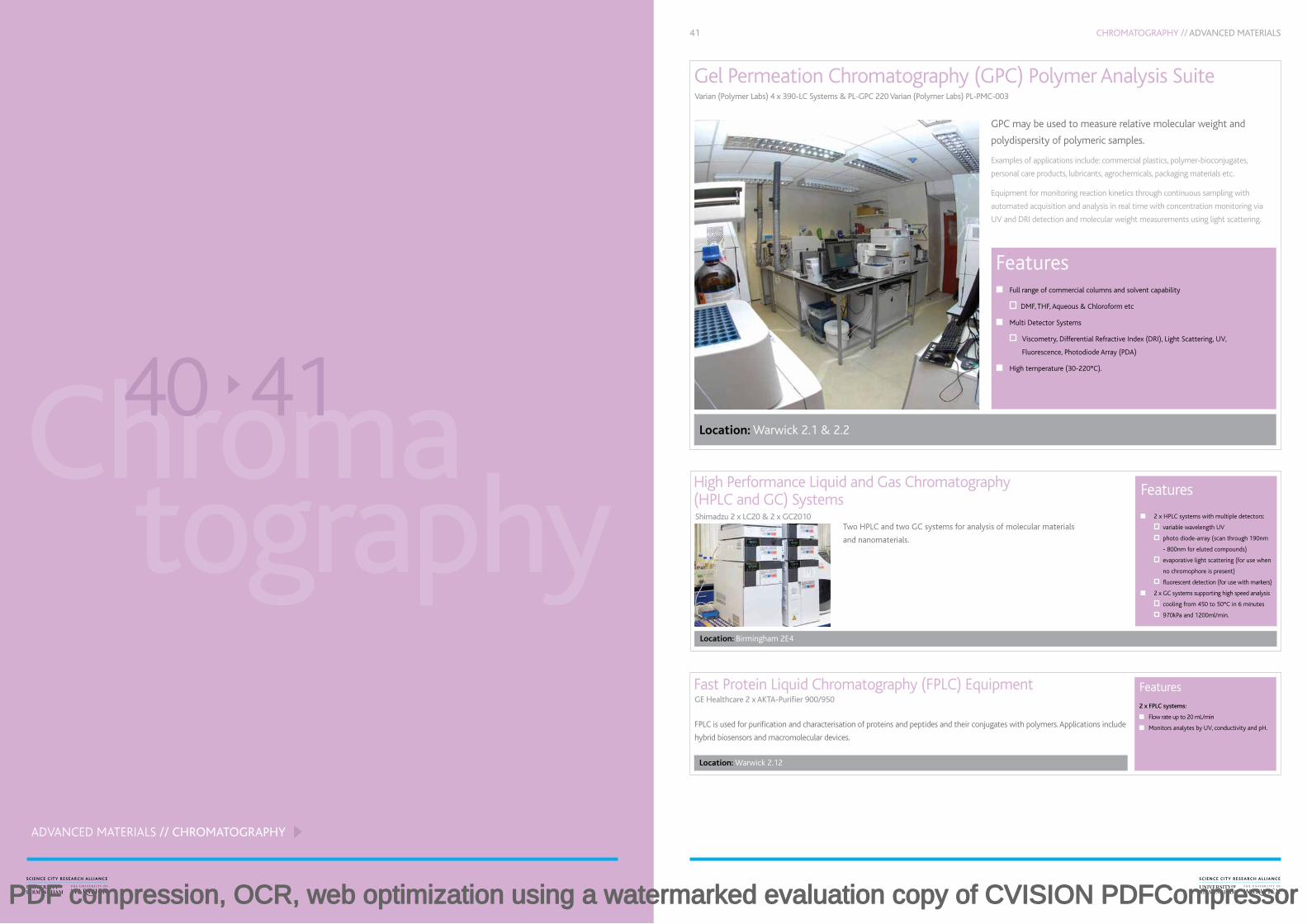
Gel Permeation Chromatography (GPC) Polymer Analysis SuiteVarian (Polymer Labs) 4 x 390-LC Systems & PL-GPC 220 Varian (Polymer Labs) PL-PMC-003
GPC may be used to measure relative molecular weight and
polydispersity of polymeric samples.
Examples of applications include: commercial plastics, polymer-bioconjugates,
personal care products, lubricants, agrochemicals, packaging materials etc.
Equipment for monitoring reaction kinetics through continuous sampling with
automated acquisition and analysis in real time with concentration monitoring via
Uv and DRI detection and molecular weight measurements using light scattering.
Full range of commercial columns and solvent capability
DMF, THF, Aqueous & Chloroform etc
Multi Detector Systems
viscometry, Differential Refractive Index (DRI), Light Scattering, Uv,
Fluorescence, Photodiode Array (PDA)
High temperature (30-220°C).
Features
Location: Warwick 2.1 & 2.2
Fast Protein Liquid Chromatography (FPLC) EquipmentGE Healthcare 2 x AKTA-Purifier 900/950
FPLC is used for purification and characterisation of proteins and peptides and their conjugates with polymers. Applications include
hybrid biosensors and macromolecular devices.
2 x FPLC systems:
Flow rate up to 20 mL/min
Monitors analytes by Uv, conductivity and pH.
Features
Location: Warwick 2.12
CHROMATOGRAPHY // ADVANCED MATERIALS 41
High Performance Liquid and Gas Chromatography (HPLC and GC) SystemsShimadzu 2 x LC20 & 2 x GC2010
Two HPLC and two GC systems for analysis of molecular materials
and nanomaterials.
2 x HPLC systems with multiple detectors:
variable wavelength Uv
photo diode-array (scan through 190nm
- 800nm for eluted compounds)
evaporative light scattering (for use when
no chromophore is present)
fluorescent detection (for use with markers)
2 x GC systems supporting high speed analysis
cooling from 450 to 50°C in 6 minutes
970kPa and 1200ml/min.
Features
Location: Birmingham 2E4
Chromatography
ADvANCED MATERIALS // CHROMATOGRAPHY
40 41
PDF compression, OCR, web optimization using a watermarked evaluation copy of CVISION PDFCompressor

43
Particle Size and Shape AnalyserQICPIC and HELOS/BF Sympatec
Equipment for the characterisation of particulate systems including both dry and
wet samples including suspensions, powders and emulsions.
High speed analysis of particle size distribution is possible. Shape analysis yields
aspect ratio and sphericity.
Particle size 1μm to 6μm
Aerodispersions, sprays
High-speed camera: up to 500Hz
Study of agglomerated fine and cohesive
powders: 1μm to 6μm
Laser diffraction sensor 0.1μm - 875μm for
wet and dry samples.
Features
Location: Birmingham 2E18
Dark Field Particle TrackerNanosight LM10
Particle sizing using Brownian motion tracking for a variety of applications, including ceramics, viruses, colloidal suspensions,
polymer nanoparticles, and wear debris in lubricants.
Particles illuminated by 40mW 640nm laser
tracked and quantified by software
Size range typically 10 - 1000nm
Sample volume 0.3ml
Polydisperse and multimodal systems identifiable.
Features
Location: Warwick & Birmingham 2.20 & 2E6
Dynamic Light Scattering Zetapotential ApparatusMalvern Instruments Nano-ZS
Measures size and zeta potential of colloids to give information on stability, polydispersity of nanoparticles, and presence of
aggregates (e.g. of proteins). Can be used in analysing size of colloids and nanoparticles, pigments and inks, Protein size,
proteomics, melting point, colloid stability, water treatment, isoelectric point determination.
Measures hydrodynamic size and zeta potential
Particle size (0.6nm - 6μm diameter) over the
molecular weight range (1000 - 2x10⁷ Da)
Temperature control 0 - 90°C
4mW HeNe laser 632.8nm.
Features
Location: Warwick 2.21
High RPM Disc CentrifugeCPS Instruments AS200 and Analytik DC24000
Measures particle size via sedimentation behaviour. Applications include polymer latexes and emulsions, silica dispersions,
micro-encapsulated drugs, pigments, and starch particles.
Size range approximately 5nm - 50μm
depending on density
Dynamic range (ratio of largest to smallest sizes)
~ 70 with constant centrifuge speed
Maximum speed 24,000rpm
High resolution (can separate 2% size difference).
Features
Location: Warwick & Birmingham 2.22 & 2E39
Powder Particle Sizer Malvern Instruments 2000 System
Measures particle radius of a variety of wet or dry powders, dispersions or emulsions by laser diffraction.
Size range 0.2μm - 2000μm
Sizing on emulsions, suspensions and
dry powders
Dual wavelength; HeNe (red) and solid state
(blue) lasers.
Features
Location: Warwick 2.23
Zeta Potentiometer and Molecular Weight CharacteriserBeckman Coulter Delta Nano C
Instrument for analysing charge and size of nanoparticles.
Particle size: 0.6nm - 7μm
Zetapotential: -100mv - +100mv
Concentration 0.001 - 40%
pH 1 - 13
Temperature: 10 - 90°C.
Features
Location: Birmingham 2E7
PARTICLE SIZE & SHAPE // ADVANCED MATERIALS
Particlesize
shape&
ADvANCED MATERIALS // PARTICLE SIZE & SHAPE
42 43
PDF compression, OCR, web optimization using a watermarked evaluation copy of CVISION PDFCompressor

BIOANALYSIS // ADVANCED MATERIALS 45
Surface Plasmon Resonance (SPR) EquipmentReichert SR7000DC
Surface Plasmon Resonance (SPR) measures biomolecular interactions providing
high quality, real time kinetic data requiring no tags or labelling of compounds or
proteins. Example application include the study of proteins, antibodies, peptides,
DNA or lipids as well as investigating drug binding or antibody-antigen interactions.
Real-time simultaneous dual-channel SPR
Temperature range: 10 - 90ºC
Sample loop: 10μL - 2mL
Flow rate: 1μL/hr - 10mL/min.
Features
Location: Birmingham 2E32
Gel Electrophoresis Kit Genetic Research Instrumentation (GRI)Alpha-Imager HP System
High resolution fluorescent and visible imaging for culture plate & microplate based arrays.
Motorised lens
Incident white light for focussing and positioning
Dual wavelength transilluminator
White light table
Five-position filter wheel.
Features
Location: Birmingham 2E11
BioanalyserAgilent 2100
A microfluidics-based platform for sizing, quantification and quality control of DNA, RNA, proteins and cells. Example applications:
characterisation of protein sensors – lab on a chip technology
10-12 samples in parallel
30-40 min analysis time.
Features
Location: Warwick 2.13
Microwave Reaction StationCEM Discoverer S-Class
The reaction station allows up to 48 microwave reactions to take place simultaneously for chemical syntheses, including polymers
and peptides.
10, 35, 80ml capacity at 21 bar, or 125ml at
atmospheric pressure
Manual peptide solid phase synthesis accessory
Gas (H2/CO) addition accessory.
Features
Location: Birmingham 2E17
Laser vibrometerPolytec OFV-5000
Measures vibration amplitude, frequency and spatial location to give full vibration mapping of an object under test. The integral
video camera can be used to monitor the area and provide a captured image for superimposition of the vibration data. Used for
the evaluation of the design of dental instrumentation such as ultrasonic scalers and dental drills.
Frequency range from near DC to 24MHz
velocities to ± 10m/s
Displacements from the sub-nanometer to
meter range.
Features
Location: Birmingham 2E35
Bioanalysis
ADvANCED MATERIALS // BIOANALYSIS
44 45
PDF compression, OCR, web optimization using a watermarked evaluation copy of CVISION PDFCompressor