Embed Size (px)
Citation preview

JOURNAL OF LIGHTWAVE TECHNOLOGY, VOL. 24, NO. 5, MAY 2006 2207
Fabrication of Add–Drop Filters Based onFrequency-Matched Microring Resonators
Tymon Barwicz, Member, OSA, Miloš A. Popovic, Student Member, IEEE, Student Member, OSA,Michael R. Watts, Member, OSA, Peter T. Rakich, Erich P. Ippen, Fellow, IEEE, Fellow, OSA,
and Henry I. Smith, Fellow, IEEE, Member, OSA
Abstract—Frequency mismatches between resonators signifi-cantly impact the spectral responses of coupled resonator filters,such as high-order microring filters. In this paper, techniquesallowing fabrication of frequency-matched high-index-contrastresonators are proposed, demonstrated, and analyzed. The mainapproach consists of inducing small dimensional changes in theresonators through alteration of the electron-beam dose usedto expose either the actual resonator on a wafer or its imageon a lithographic mask to be later used in filter fabrication.Third-order microring filters fabricated in silicon-rich silicon ni-tride, with optical resonator frequencies matched to better than1 GHz, are reported. To achieve this, the average ring-waveguidewidths of the microrings are matched to within less than 26 pmof a desired relative width offset. Furthermore, optimization andcalibration procedures allowing strict dimensional control andsmooth sidewalls are presented. A 5-nm dimensional control isdemonstrated, and the standard deviation of sidewall roughnessis reduced to below 1.6 nm.
Index Terms—Add–drop filters, coupling-induced frequencyshifts (CIFS), electron-beam (e-beam) proximity effects, fabrica-tion, microring resonators.
I. INTRODUCTION
H IGH-INDEX-CONTRAST microring resonators allowfor compact optical filters. Of particular interest to
modern optical networks are optical add–drop filters that canbe used for wavelength division multiplexing applications.Such add–drop filters must show, among other requirements,low input-to-drop-port loss (< 3 dB), high in-band extinctionin the through port (> 30 dB), and a wide free spectralrange (FSR) (> 30 nm). Frequency mismatches betweenresonators significantly alter the spectral responses of high-order microring filters [1]–[3]. In particular, the throughresponse is the most affected and becomes inadequate foradd–drop multiplexing applications. As a matter of fact, nearlyall high-order microring filters reported in the literature havebeen aimed toward drop-only applications without mention ofthe through response [4]–[6].
In previous work [3], we found the frequency mismatchbetween microring resonators to be mainly due to coupling-induced frequency shifts (CIFS) [1], electron-beam (e-beam)proximity effects, and scanning e-beam lithography (SEBL)
Manuscript received October 4, 2005; revised January 6, 2006. This workwas supported in part by Pirelli, Milan, Italy.
The authors are with the Research Laboratory of Electronics, MassachusettsInstitute of Technology, Cambridge, MA 02139 USA (e-mail: [email protected]).
Digital Object Identifier 10.1109/JLT.2006.872298
discretization errors. The first is an optical effect due to theperturbation at a coupler of the effective-index of the ringwaveguide by the bus waveguide. The two others are litho-graphic imperfections. As a result, in a third-order microringfilter, the middle microring exhibits a higher resonant frequencythan the outer rings.
In this paper, techniques allowing fabrication of frequency-matched high-index-contrast resonators are proposed, demon-strated, and analyzed. The frequency matching is mainlyperformed by introducing slight and accurate dimensionalchanges in the resonators through alteration of the e-beamdose used to expose the actual resonator on a wafer or itsimage on a lithographic mask to be later used in filter fab-rication. The expected frequency mismatch due to CIFS ande-beam proximity effects as well as the required e-beam-dosealteration for frequency matching are calculated. Calculatedand experimentally observed parameters are compared, andexcellent agreement is observed considering the complexity ofthe problem. Third-order microring filters fabricated by SEBLin silicon-rich silicon nitride (SiN) with resonators matched tobetter than 1 GHz are reported. The average ring-waveguidewidths of these resonators are matched within 26 pm of a de-sired relative width offset. The frequency-matching techniqueallowed fabrication of third-order microring filters with 17-dBthrough-port extinction, which is the highest reported in theliterature. When these filters are arranged in the cascaded con-figuration for which they were designed, the through extinctionexceeds 30 dB [7].
A detailed treatment of resonance frequency control inmicroring filters is presented. The filter performance is quan-titatively related to fabrication parameters. In addition, opti-mization and calibration procedures allowing strict dimensionalcontrol and smooth sidewalls are presented. A 5-nm dimen-sional control and a standard deviation of sidewall roughnessbelow 1.6 nm are demonstrated. Furthermore, the e-beamwriting strategy is optimized for microrings, and the e-beamproximity function is experimentally acquired.
II. STRUCTURES TO BE FABRICATED
Our goal was to create add–drop filters with a 40-GHz band-width, less than 0.1-dB passband ripple, a 20-nm FSR, and a30-dB rejection at the adjacent channels (assuming a 100-GHzchannel spacing). Third-order filters were designed with aflattop (Chebyshev) drop-port response using known synthesistechniques [8]. The coupling gaps were obtained using
0733-8724/$20.00 © 2006 IEEE

2208 JOURNAL OF LIGHTWAVE TECHNOLOGY, VOL. 24, NO. 5, MAY 2006
Fig. 1. Schematic of a series-coupled third-order microring filter. The mi-crorings are designed to be alike. The actual parameters used are presented inTable I. (a) Top view and (b) cross section of the waveguides at the bus-to-ringcoupling region.
TABLE IDESIGNED FILTER PARAMETERS
three-dimensional (3-D) finite-difference-time-domain (FDTD)simulations. The design details are reported in [7] and [9].
A series-coupled third-order microring filter is shown inFig. 1. The waveguides are formed of an SiN core, a siliconoxide undercladding, and an air topcladding. The designedfilter dimensions are shown in Table I. First, frequency-matchedmicroring filters were demonstrated with a symmetric couplerdesign (SCD) employing identical bus-waveguide and ring-waveguide cross sections [9]. Then, the design was improvedto further reduce the filter loss with an asymmetric couplerdesign (ACD) that reduced coupler scattering and a wider ringwaveguide that reduced bending loss [7]. Coupler scatteringwas found to be the main source of filter loss in our previouswork [3]. Fabrication of both microring structures is reported inthe present paper.
Fig. 2. Fabrication-process overview. (a) Initial multilayer formed from3 µm of silicon oxide, 400 nm of silicon-rich silicon nitride (SiN), 200 nm ofPMMA, and 60 nm of Aquasave [10]. (b) SEBL exposure, Aquasave removal,and PMMA development. (c) 45-nm Ni evaporation. (d) Liftoff. (e) Reactive-ion etching and Ni removal.
III. PROCESS OVERVIEW
The fabrication process is shown in Fig. 2. First, a Si waferis thermally oxidized to form a 3-µm-layer of SiO2. Then, a400-nm-thick SiN layer is deposited by low-pressure chemicalvapor deposition (LPCVD) in a vertical thermal reactor with agas mixture of SiH2Cl2 and NH3. The resulting SiN shows lowstress and is often referred to as the low-stress nitride. Next,200 nm of poly-methyl-methacrylate (PMMA) and 60 nm ofAquasave are spun on. PMMA is a positive e-beam resist whileAquasave [10] is a water-soluble conductive polymer usedto prevent charging during SEBL. The PMMA is exposed at30 keV using a Raith 150 SEBL system. The Aquasave isremoved, and the PMMA developed. Next, 45 nm of Ni isevaporated on the structure, and a liftoff is performed byremoving the nonexposed PMMA. Using the Ni as a hardmask,the waveguides are defined by conventional reactive-ion etching(RIE) with a gas mixture of CHF3-O2. To obtain an accurateetch depth, RIE is performed in several steps, in between whichthe etch depth is measured with a profilometer. Finally, the Ni isremoved using a nitric-acid-based commercial wet Ni etchant,and the sample is prepared for optical characterization.
IV. SIDEWALL SMOOTHNESS
A. Liftoff Optimization
In the previous work, we found that liftoff is the fabricationstep generating the most line-edge roughness (LER) [11]. Thisroughness is then transferred to the core material during RIEto form the biggest component of the sidewall roughness. Atbest, the LER of a lifted-off hardmask line will conform to theresist. However, coarse-material microstructure and coverageof the resist sidewall with the evaporated material worsen theLER of the hardmask. The material microstructure can bemanaged with appropriate e-beam evaporation parameters andsurface cleanliness. The resist-sidewall coverage depends onthe geometry of the e-beam evaporator and the angle of theresist sidewall. In most cases, the geometry of the evaporatorcannot be altered and the resist-sidewall angle is the mainliftoff-optimization parameter.

BARWICZ et al.: FABRICATION OF ADD–DROP FILTERS BASED ON MICRORING RESONATORS 2209
Fig. 3. Impact of resist profile on sidewall roughness. An undercut in the resistprofile is desired but must be kept small. Schematic cross section of evaporatedNi on (a) single PMMA layer and (b) double PMMA layer. Top-view electronmicrograph of resulting Ni liftoff for (c) single PMMA layer and (d) doublePMMA layer. A second Ni line appears if the resist undercut is too strong.This second Ni line is partially sputtered during etching and contributes to in-creased sidewall roughness. Resulting waveguide sidewalls from a Ni hardmask(e) without and (f) with a secondary Ni line.
With sufficiently high e-beam dose, an undercut can be cre-ated in the resist. Electrons backscattered by the core materialincrease the dose delivered near the resist-dielectric interface.This undercut is helpful in reducing sidewall coverage and,thus, LER. A sharper undercut can be obtained by using adouble-layer resist with the most sensitive resist on the bottomof the double layer. In our case, a double layer was investi-gated with two PMMA resists of different molecular weights:950 kg/mol on top and 495 kg/mol on the bottom. The lowerthe molecular weight is, the more sensitive the PMMA.
Ni, Cr, and Al were investigated as hardmask materials. Ofthe three, Ni was found to provide the best liftoff results. Crshowed high-enough stress to pull on the PMMA and alter thesidewall angle while Al was too soft to be used as a hardmaskfor our applications. Surprisingly, the double-layer resist wasfound not to be useful for Ni liftoff. A sharp-resist profile isdesired but the undercut needs to be small. As shown in Fig. 3,for strong undercuts, a thin Ni layer is formed on the edge ofthe hardmask. This layer gets partially sputtered during RIEand worsens the sidewall roughness. The formation of the thinlayer can be explained by the sizeable energy of the e-beamevaporated Ni atoms providing them with the needed surfacemobility to diffuse into the region shadowed by the upper part ofthe resist. This secondary Ni line is also formed when exposinga single resist layer with high electron doses.
In the present work, a single layer of 950-kg/mol PMMAwas used. The e-beam dose was selected to be the highest onenot triggering the formation of the thin secondary Ni layer. ThePMMA was developed in a 2:1 mixture of isopropanol alcohol(IPA) to methyl iso-butyl ketone (MIBK) for 60 s at 21 ◦C. Alower portion of MIBK provides a higher contrast developer butincreases the LER of the PMMA and should be avoided [12].
B. Reactive-Ion-Etching Optimization
To obtain smooth and vertical sidewalls, adequate side-wall polymerization (passivation) and hardmask erosion arerequired. The sidewall polymerization is controlled through
TABLE IIMEASURED SIDEWALL ROUGHNESS
the amount of O2 in the CHF3-O2 gas mixture. The higherthe O2 content is, the weaker the polymerization. When thepolymerization is too low, the sidewalls will be curved inwardsand the hardmask undercut, which fosters mask erosion androughness. When the polymerization is too high, the sidewallswill be straight but slanted with a wider base than top. A 16-to-3-sccm ratio of CHF3 to O2 was found optimal for SiN etching.
Mask erosion is known to be an important source of sidewallroughness. Surprisingly, it should not be strictly minimized.When using a Ni hardmask, the hardmask-to-SiN etching selec-tivity can be very high. We found that a controlled sputtering ofthe Ni hardmask can reduce the sidewall roughness presumablyby polishing the hardmask during the RIE. Using a Plasmath-erm 790 etcher, a 500-V bias resulting in a power of about300 W was found to be optimal. It reduced the SiN:Ni etchingratio to about 50:1.
C. Resulting Sidewall Smoothness
The spectral density of the sidewall roughness was measuredusing the technique described in [11]. In most cases, the side-wall roughness can be well approximated by a one-dimensional(1-D) distribution with zero-mean called f(z). It represents theexcursion of the real edge from an idealized straight edge. Thenature of roughness is described by the autocorrelation functionof f(z)
R(u) = 〈f(z)f(z + u)〉
where z is the position along the waveguide, and the bracketsrepresent the ensemble average. Typically, R(u) can be wellapproximated [11], [13] by an exponential model
R(u) ≈ σ2 exp(−|u|
Lc
)
where σ2 is the roughness variance, and Lc is the correlationlength. A large Lc is indicative of strongly represented lowspatial frequencies in the spectral density of roughness. Asscattering losses due to sidewall roughness are triggered bythese low spatial frequencies of roughness [14], the smaller theLc is, the lower the scattering losses [15].
Measured values of σ2 and Lc are presented in Table II. Theroughness measurements were performed on bus-waveguidesof actual filters. Fabrication of the SCD and ACD filters wasseparated by several months and the process was reoptimized toachieve smoother sidewalls on the later fabricated ACD filters.
2210 JOURNAL OF LIGHTWAVE TECHNOLOGY, VOL. 24, NO. 5, MAY 2006
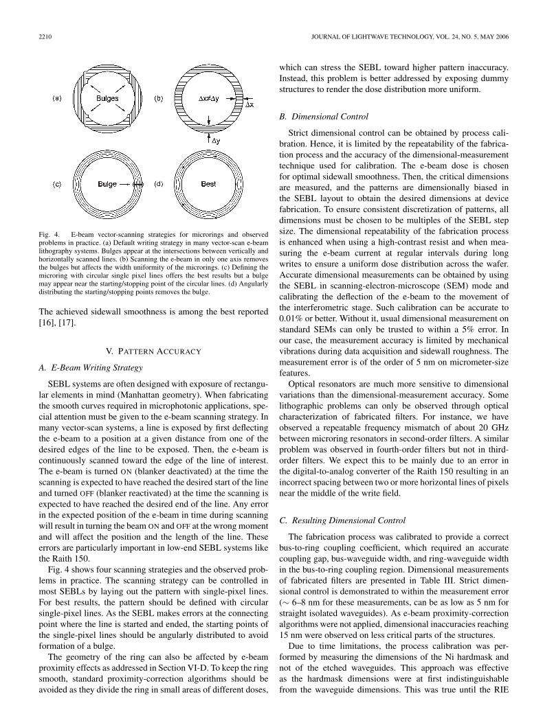
Fig. 4. E-beam vector-scanning strategies for microrings and observedproblems in practice. (a) Default writing strategy in many vector-scan e-beamlithography systems. Bulges appear at the intersections between vertically andhorizontally scanned lines. (b) Scanning the e-beam in only one axis removesthe bulges but affects the width uniformity of the microrings. (c) Defining themicroring with circular single pixel lines offers the best results but a bulgemay appear near the starting/stopping point of the circular lines. (d) Angularlydistributing the starting/stopping points removes the bulge.
The achieved sidewall smoothness is among the best reported[16], [17].
V. PATTERN ACCURACY
A. E-Beam Writing Strategy
SEBL systems are often designed with exposure of rectangu-lar elements in mind (Manhattan geometry). When fabricatingthe smooth curves required in microphotonic applications, spe-cial attention must be given to the e-beam scanning strategy. Inmany vector-scan systems, a line is exposed by first deflectingthe e-beam to a position at a given distance from one of thedesired edges of the line to be exposed. Then, the e-beam iscontinuously scanned toward the edge of the line of interest.The e-beam is turned ON (blanker deactivated) at the time thescanning is expected to have reached the desired start of the lineand turned OFF (blanker reactivated) at the time the scanning isexpected to have reached the desired end of the line. Any errorin the expected position of the e-beam in time during scanningwill result in turning the beam ON and OFF at the wrong momentand will affect the position and the length of the line. Theseerrors are particularly important in low-end SEBL systems likethe Raith 150.
Fig. 4 shows four scanning strategies and the observed prob-lems in practice. The scanning strategy can be controlled inmost SEBLs by laying out the pattern with single-pixel lines.For best results, the pattern should be defined with circularsingle-pixel lines. As the SEBL makes errors at the connectingpoint where the line is started and ended, the starting points ofthe single-pixel lines should be angularly distributed to avoidformation of a bulge.
The geometry of the ring can also be affected by e-beamproximity effects as addressed in Section VI-D. To keep the ringsmooth, standard proximity-correction algorithms should beavoided as they divide the ring in small areas of different doses,
which can stress the SEBL toward higher pattern inaccuracy.Instead, this problem is better addressed by exposing dummystructures to render the dose distribution more uniform.
B. Dimensional Control
Strict dimensional control can be obtained by process cali-bration. Hence, it is limited by the repeatability of the fabrica-tion process and the accuracy of the dimensional-measurementtechnique used for calibration. The e-beam dose is chosenfor optimal sidewall smoothness. Then, the critical dimensionsare measured, and the patterns are dimensionally biased inthe SEBL layout to obtain the desired dimensions at devicefabrication. To ensure consistent discretization of patterns, alldimensions must be chosen to be multiples of the SEBL stepsize. The dimensional repeatability of the fabrication processis enhanced when using a high-contrast resist and when mea-suring the e-beam current at regular intervals during longwrites to ensure a uniform dose distribution across the wafer.Accurate dimensional measurements can be obtained by usingthe SEBL in scanning-electron-microscope (SEM) mode andcalibrating the deflection of the e-beam to the movement ofthe interferometric stage. Such calibration can be accurate to0.01% or better. Without it, usual dimensional measurement onstandard SEMs can only be trusted to within a 5% error. Inour case, the measurement accuracy is limited by mechanicalvibrations during data acquisition and sidewall roughness. Themeasurement error is of the order of 5 nm on micrometer-sizefeatures.
Optical resonators are much more sensitive to dimensionalvariations than the dimensional-measurement accuracy. Somelithographic problems can only be observed through opticalcharacterization of fabricated filters. For instance, we haveobserved a repeatable frequency mismatch of about 20 GHzbetween microring resonators in second-order filters. A similarproblem was observed in fourth-order filters but not in third-order filters. We expect this to be mainly due to an error inthe digital-to-analog converter of the Raith 150 resulting in anincorrect spacing between two or more horizontal lines of pixelsnear the middle of the write field.
C. Resulting Dimensional Control
The fabrication process was calibrated to provide a correctbus-to-ring coupling coefficient, which required an accuratecoupling gap, bus-waveguide width, and ring-waveguide widthin the bus-to-ring coupling region. Dimensional measurementsof fabricated filters are presented in Table III. Strict dimen-sional control is demonstrated to within the measurement error(∼ 6–8 nm for these measurements, can be as low as 5 nm forstraight isolated waveguides). As e-beam proximity-correctionalgorithms were not applied, dimensional inaccuracies reaching15 nm were observed on less critical parts of the structures.
Due to time limitations, the process calibration was per-formed by measuring the dimensions of the Ni hardmask andnot of the etched waveguides. This approach was effectiveas the hardmask dimensions were at first indistinguishablefrom the waveguide dimensions. This was true until the RIE

BARWICZ et al.: FABRICATION OF ADD–DROP FILTERS BASED ON MICRORING RESONATORS 2211
TABLE IIIMEASURED DIMENSIONS
process was reoptimized to improve the sidewall smoothnessbefore fabrication of the ACD filters. The resulting RIE processprovided for a more slanted sidewall (∼ 86◦), and the hard-mask dimensions corresponded to dimensions at the top of thewaveguides and not at the midheight of the waveguides. There-fore, in order to express the performance of the dimensionalcalibration itself, the dimensional measurements in Table IIIare reported at midheight of the waveguides for the SCD filtersand at the top of the waveguides for the ACD filters. The latterwaveguides were about 26 nm larger at the midheight thanat the top when isolated. In the high-aspect-ratio bus-to-ringcoupling gap, the sidewalls were more vertical and the couplinggap was reduced at midheight by about 16 nm. The differenceis attributed to weaker sidewall polymerization in high-aspect-ratio trenches.
VI. RESONANCE FREQUENCY MATCHING
A. Frequency-Matching Strategy
Frequency mismatch between microring resonators can bedue to CIFS [1], e-beam proximity effects, SEBL discretizationerrors, SEBL intrafield distortions, and SEBL digital-to-analog-converter errors.
As optical- and imprint-lithography masks are usually madeby SEBL, all of the above mechanisms are expected to intro-duce frequency shifts even if the microrings are fabricated usingoptical or imprint lithography instead of SEBL. However, whenoptical projection lithography is used, the dimensional errorson the mask will be reduced by the demagnification factor ofthe projection system (usually 4 or 5×). Proximity-correctionalgorithms are typically applied in mask manufacturing. How-ever, even if they help reduce frequency shifts due to e-beamproximity effects, they cannot eliminate these shifts as theycorrect the e-beam-dose distribution to first order only [18],which is insufficient for frequency matching.
The SEBL discretization errors can be eliminated by choos-ing all device dimensions to be multiples of the SEBL step size.All the remaining frequency-shift sources can be compensatedby properly adjusting the middle-microring resonant frequency.The dimensional alteration required for such a correction ismuch smaller than the SEBL step size and cannot be obtainedby changing the middle-ring dimensions in the SEBL layout.
Fig. 5. Frequency-matching strategies. (a) SEBL dose of the middle ringis increased to precisely widen the middle-ring waveguide. (b) Secondarynonresonant ring is introduced at the center of the middle ring to increase theeffective index of the middle ring waveguide. Both methods lower the resonantfrequency of the middle ring to match it to the outer rings. (a) is particularlyuseful if a maskless lithography technique, such as SEBL, is used and can beapplied in either mask fabrication or direct device writing. (b) is particularlyuseful for photolithography or nanoimprint lithography when little control isexerted on the mask-manufacturing process.
However, such a small, precise, and accurate dimensional al-teration can be introduced by changing the e-beam dose usedat exposure of the middle microring. By increasing the middle-ring dose, the width of the ring waveguide is increased slightlyand the middle-ring resonance frequency can be lowered tomatch it to the outer microrings. This dose compensation can beintroduced when using direct-write SEBL or when fabricatinga lithographic mask for optical or imprint lithography.
When optical or imprint lithography is used and little controlis exerted on the mask fabrication, the middle-microring reso-nant frequency can be adjusted by changing the effective indexof the ring waveguide without attempting to precisely correct itsdimensions. A secondary nonresonant ring can be introduced inthe center of the middle microring to increase its effective indexand lower its resonance frequency to match it to the outer rings.
The two frequency-correction approaches are illustrated inFig. 5. In the present work, only e-beam dose compensationwas used.
B. Proximity Function
The exact e-beam dose compensation required for frequencymatching of the microrings is best found empirically by fab-ricating and optically characterizing a number of filters withvarious dose compensations. However, to reduce the numberof empirical iterations needed and better understand the under-lying physical phenomena, knowledge of the e-beam proximityfunction is desired. The e-beam proximity function describesthe spatial distribution of the resist exposure around the centerof the e-beam. Its shape results from the interaction of thee-beam with matter. The knowledge of this shape allows us toestimate the frequency mismatch due to the e-beam proximityeffects and the dose compensation needed for frequency match-ing. These two quantities cannot be usefully estimated fromdimensional measurements, which lack the required accuracy.
The proximity function was found empirically using twodifferent methods. First, large rings [Fig. 6(a)] were exposedwith various inner radii and e-beam doses [19]. The rings wereinspected with an SEM, and the minimum ring dose required tofully develop the resist in the middle of a ring with a given innerradius was noted. Second, isolated dots [Fig. 6(b)] were ex-posed with various e-beam doses, and their radii were measured

2212 JOURNAL OF LIGHTWAVE TECHNOLOGY, VOL. 24, NO. 5, MAY 2006
Fig. 6. Two empirical methods used to obtain the e-beam proximity function.(a) Large rings were exposed with various inner radii and doses. The lowestring dose clearing the center of the ring was noted. (b) Dots were exposed atvarious doses, and their radii were measured. The pole in the middle of the dot(fallen on its side) is characteristic of PMMA exposed at high doses where itbecomes highly cross linked and insoluble to the resist developer.
with an SEM [20]. All exposures were performed on the multi-layer of interest [Fig. 2(a)] with a Raith 150 SEBL operating at30 keV. The PMMA was developed with 3:1 IPA:MIBK, whichis a higher contrast developer than the one used for microringfabrication, as resist contrast was more important for this ap-plication than line-edge smoothness. Then, the samples werecoated with a thin (2–3 nm) layer of Au-Pd to prevent chargingduring the SEM analysis.
The proximity function f(r) is a monotonically decreasingfunction normalized so
∞∫0
f(r)2πrdr = 1
where r is the distance from the center of the e-beam to thepoint of interest. Most often, it is assumed to follow a double-Gaussian model [21]
f0(r) =1
π(1 + η)
(1α2
exp(−r2
α2
)+
η
β2exp
(−r2
β2
))
(1)
where α < β and where the first Gaussian accounts for forwardelectron scattering and the second Gaussian accounts for back-ward electron scattering.
The experimental results obtained with the large rings arepresented in Fig. 7(a). The required ring dose D to reach, at thecenter of the ring, the resist clearing dose D0 is given by
D =D0∫ R2
R1f(r)2πrdr
D0∫ ∞R1
f(r)2πrdr, for R2 > 3β
where R1 and R2 are the inner and outer ring radii, respectively.Most often, R2 is chosen to be large enough for the upper limitof the integration to be approximated by infinity. In the presentexperiments, R2 = 18 µm was used.
The experimental results obtained with the dots are presentedin Fig. 7(b). The dot dose ddot and the dot radius rdot are related
Fig. 7. Experimentally obtained e-beam proximity function. (a) Resultsobtained with large ring exposures and (b) results obtained with dot exposures.The standard double-Gaussian model of the e-beam proximity function is notappropriate, as seen in (b). The model was corrected with the tail functionpresented in (2). The fitted parameters are reported in Table IV.
to the proximity function by
f(rdot) =D0
ddot
(10−8 cm2/µm2
)
where rdot is expressed in µm, f(r) is expressed in µm−2, D0
is expressed in µC/cm2, and ddot is expressed in µC.Exposing large rings was found to be particularly useful
for probing the proximity function at long interaction lengths(R1 > 1 µm). For small R1, identifying the needed ring doseaccurately is difficult as a particle can be mistaken for remain-ing resist. On the other hand, exposing the dots was foundparticularly useful for short to medium interaction lengths(40 nm < rdot < 1 µm). For longer interactions, the exposurecontrast becomes too low at the clearing dose for the edge ofthe PMMA to be well defined (an even higher contrast resistwould be required). Below 40 nm, the measurements are alsodifficult as the feature size gets close to the resist resolution,and the shape of the dots is affected by imperfect stigmation ofthe e-beam.
The large rings experimental data were least square fit to thedouble-Gaussian model of (1). The best fit is shown with dotted

BARWICZ et al.: FABRICATION OF ADD–DROP FILTERS BASED ON MICRORING RESONATORS 2213
TABLE IVE-BEAM PROXIMITY-FUNCTION FITTED PARAMETERS
lines in Fig. 7(a) and (b). The fitted parameters are presentedin Table IV. As f(r) could not be probed at sufficiently shortinteraction lengths, α = 0.015 µm was assumed from simula-tion data provided by the SEBL manufacturer. The resultingfit looks acceptable in Fig. 7(a) but in Fig. 7(b), where thediscrepancy is amplified by the logarithmic scale, the double-Gaussian model looks obviously inappropriate. A similar tailin the proximity function has been reported in [20], where itwas found to be possibly due to scattering in the resist, high-energy secondary electrons, and tails in the incident e-beamdistribution. In addition, the proximity function was simulatedin [22] for the multilayer and e-beam energy of interest, and asimilar tail was observed.
The double-Gaussian model can be corrected by adding a tailfunction τ(r). Then, the proximity function becomes
f1(r) =f0(r) + τ(r)
1 +∫ ∞0 τ(r)2πrdr
.
From Fig. 7(b), we can see that the tail could be fit to apolynomial in logarithmic space. In fact, a simple exponentialis not sufficient. Hence, we choose the tail function to beof the form
τ(r)=exp(t4(ln(r))4+t3(ln(r))3+t2(ln(r))2+t1(ln(r))+t0
)(2)
where t4, t3, t2, t1, and t0 are the fitting parameters. The best fitto this corrected double-Gaussian model is shown with the solidlines in Fig. 7(a) and (b). The fitted parameters are reported inTable IV.
C. Fast Proximity-Effect Computation
To define arbitrary structures, the SEBL exposes sets ofdiscreet points (pixels). The dose at a given location D(x, y)will be given by the summation of the contributions of allexposed points weighted by the proximity function
D(x, y) =∑
i
qif1
(√(x − xi)2 + (y − yi)2
)(3)
where x and y define the location at which the dose is sought, xi
and yi define the position of an exposed point, and qi is the dosedelivered at that point. When the SEBL step size is smaller thanthe proximity-function parameter α, (3) is well approximatedby a two-dimensional (2-D) convolution
D(x, y) =Q ⊗⊗f1
=
+∞∫−∞
+∞∫−∞
Q(x′, y′)f1
(√(x − x′)2 +(y − y′)2
)dx′dy′
where Q is the dose profile laid out in the SEBL. For arbitrarypatterns, the 2-D convolution needs to be computed numeri-cally. However, even with the best algorithms, a numerical 2-Dconvolution requires a large number of operations and is notwell suited for computation of small dimensional changes inlarge structures like microring resonators. For microring filters,the following semi-analytical method can greatly simplify thecomputational problem. It takes advantage of the fact thatmicroring filters are formed of 1-D elements. Microrings are1-D elements in cylindrical coordinates and infinitely longand straight bus waveguides are 1-D elements in Cartesiancoordinates. Bus waveguides oriented along the y axis can beassumed infinitely long and straight if they extend straight tomore than 3β (∼ 12 µm) above and below y. Then, the doseprofile resulting from exposing with unit dose a bus waveguidesoriented along the y axis and centered at the origin is given by
Fbus(x) =
+wbus2∫
−wbus2
f(x − x′)dx′
while the dose profile resulting from exposing with unit dose amicroring centered at the origin is given by
Fring(r) =
R∫R−wring
2π∫0
f(√
r′2 + r2 − 2r′r cos θ′)
dθ′r′dr′.
The above form of convolution in cylindrical coordinates isvalid when the convolved functions are angularly invariant [23].The complete dose profile is given by
D(x, y) =∑
j
QjFbus(x − xj)
+∑
k
QkFring
(√(x − xk)2 + (y − yk)2
)
where Qj and Qk are the area doses defined in the SEBL layoutfor each element (ring or waveguide), xj defines the middle ofeach bus waveguide, and xk and yk define the center of eachmicroring.
D. Predicted Microring Shapes
Using the fast proximity-effects computation presentedabove, the dose profile was computed for the two filter struc-tures addressed in this paper. The shape of the microrings and

2214 JOURNAL OF LIGHTWAVE TECHNOLOGY, VOL. 24, NO. 5, MAY 2006
Fig. 8. Resist clearing-dose contours for various SEBL area doses expressedas relative offsets from the dose minimizing the width variations in all ringwaveguides of a filter. The ring-waveguide edges will follow the clearing-dosecontours but will be consistently offset by the fabrication process. The dottedlines represent the positions of the ring-waveguide edges in the SEBL layoutand take into account the width bias used in fabrication. The shaded areascorrespond to regions exposed by the SEBL. (a) Definition of angular positionsalong the outer and middle rings. (b) Clearing-dose contours for SCD filters.(c) Clearing-dose contours for ACD filters.
all relative dimensions will follow approximately the contoursof constant dose corresponding to the clearing dose of theresist. However, the absolute dimensions of the microrings willbe consistently offset from these contours by the fabricationprocess.
The microring shape is a function of the SEBL area doseused. A given SEBL area dose [the minimum-proximity-effect(MPE) dose] will minimize the width variations in all micror-ings. In the present case, it is obtained when the SEBL areadose used is about three times the clearing dose of the resist. InFig. 8, the clearing-dose contours are plotted for various SEBL
Fig. 9. (a) Predicted frequency mismatch between middle and outer micror-ings due to e-beam proximity effects. MPE dose is defined as the SEBL doseminimizing the width variation in all ring waveguides of a filter. (b) Predictedfrequency compensation resulting from an increase of the SEBL dose on themiddle ring. The base dose is the SEBL area dose used on all rings in (a) andon outer rings in (b).
doses, expressed as relative offsets from the MPE dose. As ex-pected, the ring waveguides are wider for higher e-beam doses.The largest ring-waveguide widths are obtained near the smallbus-to-ring coupling gaps while the smallest ring-waveguidewidths are obtained near the top and bottom of the middle rings[in orientation of Fig. 8(a)]. The dose profile of each filter hastwo axes of symmetry (one vertical and one horizontal) goingthrough the center of the middle ring of the filter.
When the same dose is used on middle and outer rings, thewidth of the middle ring is smaller than the width of the outerrings. Moreover, as the outer and inner radii are differentlyaffected by proximity effects, the ring circumference willbe larger in the outer rings than in the middle ring. Theseraise the resonant frequency of the middle ring and create afrequency mismatch with the outer rings. This frequency mis-match is a function of the SEBL area dose used as the shapesof the middle and outer rings are differently affected by a dosechange. This dependence is presented in Fig. 9(a). The smallestfrequency mismatch is obtained near the MPE dose. Whenthe SEBL dose used differs significantly from the MPE dose,the frequency mismatch increases sharply due to a weaker

BARWICZ et al.: FABRICATION OF ADD–DROP FILTERS BASED ON MICRORING RESONATORS 2215
Fig. 10. Predicted and measured width variations in ring waveguides ofSCD filters. The dimensional measurements were performed as explained inSection V-B. The filter is assumed to have two axes of symmetry (one verticaland one horizontal) going through the center of the middle ring. The angularpositions used are defined in Fig. 8(a).
dose-profile gradient near the resist-clearing dose resultingin larger variations of the microring shapes. To correct forfrequency mismatches due to proximity effects and all otherrepeatable sources, one can increase the dose on the middlering to reduce its resonant frequency. The resulting frequencycompensation is shown in Fig. 9(b). Note that the exactshapes of the outer and middle rings do not need to be thesame, as only the resonant frequencies need to be equal. Anestimate of the total frequency mismatch can be obtained byadding an estimate of the CIFS (usually obtained by FDTDelectromagnetic simulations) to the frequency mismatch dueto proximity effects of Fig. 9(a). Then, an estimate of the dosecompensation required is obtained from Fig. 9(b).
A dose increase on the middle ring will lower not onlythe resonant frequency of the middle ring but also, throughproximity effects, the resonant frequency of the outer rings.This phenomenon is taken into account in Fig. 9(b). For a givendose compensation, the outer rings’ resonant frequency will bedecreased by 3.0%–3.5% of the decrease of the middle ringresonant frequency.
E. Comparison of Predicted and Measured Dimensions
The width of fabricated microrings was measured in SCDfilters at several angular positions using the method described inSection V-B. During fabrication, the SEBL area dose was cho-sen to minimize the sidewall roughness. Predicted microringshapes were obtained using an estimate of the clearing dose ofthe resist, allowing us to choose the appropriate dose contours.The actual dose employed was found to be close to the MPEdose. Predicted and measured angular-width variations arecompared in Fig. 10. They agree within the measurement errorand confirm the validity of our analysis. The worst agreement isobserved near the bus-to-ring coupling gaps. It is believed to bedue to the behavior of RIE in small trenches, where sidewallpassivation is reduced leading to wider gaps than expected.Another source of possible disagreement between predictedand measured width variations is the finite chemical contrastof the resist. Resist edges would exactly follow the clearing-
dose contours only if the resist exhibited infinite chemicalcontrast. Obviously, this is not the case in practice. However,it is generally an acceptable approximation for high-contrastresists, such as PMMA.
Error bars in Fig. 10 show that a useful estimate of thefrequency mismatch cannot be obtained from dimensional mea-surements alone. For instance, in the SCD filters, a 5-nm mea-surement error on the ring-waveguide width corresponds to a200-GHz error in the resonance frequency of the correspondingmicroring.
VII. FABRICATED FREQUENCY-MATCHED FILTERS
The exact dose compensation required for frequency match-ing was obtained empirically by fabricating and opticallycharacterizing sets of filters with various dose compensationsdistributed around the expected compensation. The expecteddose compensation was estimated as described in Section VI-D.The experimental results are summarized in Figs. 11 and 12.The observed and predicted frequency mismatches and requireddose compensations are compared in Table V.
In Fig. 11, electron micrographs of frequency-matched SCDand ACD filters are shown along with spectral responses offilters with and without frequency compensation. As shownin Fig. 11(c), the filter response is overwhelmed by frequencyshifts when dose compensation is not applied. With appropriatedose compensation, the frequency mismatches were reducedto below 1 and 2 GHz for SCD and ACD filters, respectively.This allowed the highest filter through-port rejection reportedin the literature. The SCD and ACD filters showed 14 and17 dB of through rejection, respectively. The drop-port pass-band ripple is also disturbed by the frequency mismatch.However, the through-port extinction is affected first and isoverwhelmed before the passband’s ripple becomes significant.In Fig. 11(d) and (e), the passband ripple is negligible, andthe spectral oscillations are Fabry–Pérot fringes created byreflections at the chip facets.
The frequency compensation works mainly by offsetting theaverage ring width of the middle microring with respect to theouter microrings. Considering the sensitivity of the resonantfrequency with variations of the ring-waveguide width and thefrequency matching obtained, one finds that the average ring-waveguide widths are matched to a desired relative offset tobetter than 26 pm in SCD filters and to better than 68 pm inACD filters.
The designed filter bandwidth was 40 GHz. The observedfilter bandwidths were 30 and 42 GHz for the SCD and ACDfilters, respectively. The improvement in bandwidth control inthe ACD filters is due mainly to spectroscopic ellipsometermeasurements of the SiN index and thickness being madeprior to coupler design and having the design trimmed to theparameters of a given wafer chosen for fabrication. In SCDfilters, the SiN thickness and index were chosen to be 400and 2.20 nm, respectively. Then, matching these parametersin fabrication was attempted. The SiN thickness and indexused in fabrication were 406 ± 1 nm and 2.189 ± 0.003,respectively. The difference between the designed and observedfilter bandwidths is mainly due to a variation of the coupling

2216 JOURNAL OF LIGHTWAVE TECHNOLOGY, VOL. 24, NO. 5, MAY 2006
Fig. 11. Electron micrographs of fabricated frequency-matched (a) SCD filters and (b) ACD filters. Spectral responses of SCD filters (c) without dosecompensation and (d) with a 4.5% e-beam dose increase in the middle ring. (e) Spectral response of an ACD filter with a 4.2% e-beam dose increase in themiddle ring. As shown in (c), the filter response is overwhelmed by the frequency shifts when dose compensation is not applied. The predicted and requireddose compensations are compared in Table V. The resonant frequencies of the microrings of the filters reported in (d) and (e) are matched to better than 1 and2 GHz, respectively. The drop-port passband ripple introduced by such frequency mismatch is negligible, and the spectral oscillations seen in (d) and (e) areFabry–Pérot fringes created by reflections at the chip facets. The ACD improved the filter drop loss by reducing coupler scattering, which is a significant sourceof loss identified in our previous work [3].
coefficients induced by the modest discrepancy between thedesigned and deposited SiN parameters.
The drop losses observed in SCD and ACD filters were∼ 5.5 and ∼ 2.5 dB, respectively. The drop loss was improvedby the ACD by reducing the coupler scattering, which is asignificant source of loss identified in our previous work [3],and bend loss. The remaining 2.5-dB drop loss is due mainlyto a propagation loss of about 9 dB/cm. Recently, fabricationof shallow-etched ridge waveguides in thick SiN films con-firmed that the waveguide-propagation loss was mainly due toSiN material loss [24]. Based on the roughness measurementreported in Table II and on the calculations reported in [15], thescattering losses due to sidewall roughness are expected to benegligible in our filters.
In Fig. 12, the empirical relationships between frequencymismatch and dose compensation are presented. Each pointon the graphs was obtained by fitting filter spectral responses,such as the one shown in Fig. 11(c), with an analytic filtermodel. Parabolic trend lines were introduced in the graphs. Theempirical trends follow the calculated ones [shown in Fig. 9(b)]well at small dose compensations but level off at high dosecompensations. The flattening of the empirical trend is difficultto explain. Most likely, it is not due to lithographic phenom-ena but is rather caused by subsequent processing (liftoff andRIE). The insets in Fig. 12 show the data point to trend-lineexcursions that cannot be explained by measurement and fittingerrors. The frequency distribution is tighter for ACD filtersthan for SCD filters. The difference is mainly due to a bet-ter controlled fabrication process and a wider ring-waveguide
width in ACD filters (see Table I). In fact, the wider the ring-waveguide is, the smaller the frequency shifts introduced bye-beam proximity effects are. Hence, there is a clear advantagein keeping the ring-waveguide as wide as possible.
Table V compares predicted and observed frequency mis-matches and dose compensations. Considering the relative sim-plicity of the analysis when compared to the complexity ofthe problem, excellent agreement is observed. The calculatedfrequency mismatches take into account only the CIFS and thee-beam proximity effects. The difference between the calcu-lated and observed mismatches can be explained by frequency-shift sources not taken into account in the calculations, suchas SEBL intrafield distortions and SEBL digital-to-analog-converter errors. When looking at the calculated dose compen-sation required for the observed mismatch, a perfect agreementis observed for the SCD filters. For ACD filters, the dosecompensation required is underestimated in calculation. This isdue mainly to the flattening of the empirical dose-compensationtrend shown in Fig. 12(b). This flattening is stronger in ACDfilters than in SCD filters. The main difference in fabricationbetween the two filter structures is in the RIE process, wherestronger sidewall passivation was used in ACD filters than inSCD filters (as discussed in Section V-C).
Filter-to-filter frequency variations were also studied. Whenthree identical ACD filters are spaced by 100 µm, their resonantfrequencies can be matched to 2–5 GHz [7]. When the filter-to-filter spacing reaches a centimeter, the frequency can differby up to ∼ 240 GHz [25]. By analyzing the form of the driftwith filter position, we found that it was due mainly to the

BARWICZ et al.: FABRICATION OF ADD–DROP FILTERS BASED ON MICRORING RESONATORS 2217
Fig. 12. Empirical relationships between frequency mismatch and dose com-pensation for (a) SCD filters and (b) ACD filters. Data points were obtained byfitting spectral responses, such as the one shown in Fig. 11(c). Parabolic trendlines were introduced in the graphs. The insets show the data point to trend-lineexcursions that cannot be explained by measurement and fitting errors. A bettercontrolled fabrication process and wider ring-waveguide widths allowed for atighter distribution of frequencies in ACD filters.
variations in the SiN thickness. In fact, the resonant frequencywill increase by ∼ 70 GHz for a decrease of 1 nm in SiNthickness.
Wafer-to-wafer frequency variations could not be empiricallyestimated as the sample size was not statistically significant.However, the repeatability of the lithographic process can beassessed from Fig. 9. Assuming that the ratio of the base doseto the clearing dose can be controlled to 2% while the doseincrease can be controlled to 0.05%, the relative frequenciescan potentially be controlled to 1–2 GHz. This excludes thestochastic variations shown in Fig. 12.
VIII. CONCLUSION
We presented techniques allowing fabrication of frequency-matched high-index-contrast resonators, a detailed treatmentof frequency control in microring resonators, and optimizationand calibration procedures allowing strict dimensional controland smooth sidewalls. We reported third-order microring filterswith resonator frequencies matched to 1 GHz. We demonstrated5-nm dimensional control and a standard deviation of sidewallroughness below 1.6 nm. The techniques developed allowedfabrication of microring filters with low drop loss, good band-
TABLE VCOMPARISON OF CALCULATED AND OBSERVED
FREQUENCY MISMATCHES
width control, and the highest through extinction reported in theliterature. The techniques presented in this paper are of valuefor the fabrication of all types of high-index-contrast resonators.
ACKNOWLEDGMENT
The authors would like to thank F. Zhang for his help introubleshooting the Raith 150 SEBL and L. Socci for his helpin the optical characterization. This work made use of MIT’sshared SEBL facility in the Research Laboratory of Electronics(SEBL at RLE).
REFERENCES
[1] C. Manolatou, M. A. Popovic, P. T. Rakich, T. Barwicz, H. A. Haus, andE. P. Ippen, “Spectral anomalies due to coupling-induced frequency shiftsin dielectric coupled resonator filters,” in Proc. Opt. Fiber Commun.Conf., Washington, DC, 2004, pp. 379–381.
[2] M. A. Popovic, C. Manolatou, and H. A. Haus, “Coupling-induced res-onance frequency shifts in coupled dielectric multi-cavity filters,” Opt.Express, vol. 14, no. 3, pp. 1208–1222, Feb. 2006.
[3] T. Barwicz, M. A. Popovic, P. T. Rakich, M. R. Watts, H. A. Haus,E. P. Ippen, and H. I. Smith, “Microring-resonator-based add–drop filtersin SiN: Fabrication and analysis,” Opt. Express, vol. 12, no. 7, pp. 1437–1442, Apr. 2004.
[4] B. E. Little, “A VLSI photonic platform,” in Proc. Opt. Fiber Commun.Conf., Washington, DC, 2003, vol. 2, pp. 444–445.
[5] J. V. Hryniewicz, P. P. Absil, B. E. Little, R. A. Wilson, and P.-T. Ho,“Higher order filter response in coupled microring resonators,” IEEEPhoton. Technol. Lett., vol. 12, no. 3, pp. 320–322, Mar. 2000.
[6] Y. Yanagase, S. Suzuki, Y. Kokubun, and S. T. Chu, “Box-like filterresponse and expansion of FSR by a vertically triple coupled micror-ing resonator filter,” J. Lightw. Technol., vol. 20, no. 8, pp. 1525–1529,Aug. 2002.
[7] M. A. Popovic, T. Barwicz, M. R. Watts, P. T. Rakich, L. Socci,E. P. Ippen, F. X. Kärtner, and H. I. Smith, “Multistage high-ordermicroring-resonator filters with relaxed tolerances for high through-portextinction,” presented at the Conf. Lasers and Electro-Optics, Baltimore,MD, 2005, Paper CMP2.

2218 JOURNAL OF LIGHTWAVE TECHNOLOGY, VOL. 24, NO. 5, MAY 2006
[8] A. Melloni and M. Martinelli, “Synthesis of direct-coupled-resonatorsbandpass filters for WDM systems,” J. Lightw. Technol., vol. 20, no. 2,pp. 296–303, Feb. 2002.
[9] M. A. Popovic, M. R. Watts, T. Barwicz, P. T. Rakich, L. Socci,E. P. Ippen, F. X. Kärtner, and H. I. Smith, “High-index-contrast,wide-FSR microring-resonator filter design and realization withfrequency-shift compensation,” presented at the Optical Fiber Commu-nication Conf., Anaheim, CA, 2005, Paper OFK1.
[10] Mitsubishi Rayon America Inc. (2004). aquaSAVE Datasheet. [Online].Available: http://www.mrany.com
[11] T. Barwicz and H. I. Smith, “Evolution of line-edge-roughness duringfabrication of high index-contrast microphotonic devices,” J. Vac. Sci.Technol. B, Microelectron. Process. Phenom., vol. 21, no. 6, pp. 2892–2896, Nov./Dec. 2003.
[12] S. Yasin, D. G. Hasko, M. N. Khalid, D. J. Weaver, and H. Ahme,“Influence of polymer phase separation on roughness of resist features,”J. Vac. Sci. Technol. B, Microelectron. Process. Phenom., vol. 22, no. 2,pp. 574–578, Mar./Apr. 2004.
[13] F. Ladouceur, J. D. Love, and T. J. Senden, “Effect of side wall roughnessin buried channel waveguides,” Proc. Inst. Elect. Eng.—Optoelectron.,vol. 141, no. 4, pp. 242–248, Aug. 1994.
[14] D. Marcuse, “Radiation losses of dielectric waveguides in terms of thepower spectrum of the wall distortion function,” Bell Syst. Tech. J., vol. 48,no. 10, pp. 3233–3244, Dec. 1969.
[15] T. Barwicz and H. A. Haus, “Three-dimensional analysis of scatteringlosses due to sidewall roughness in microphotonic waveguides,” J. Lightw.Technol., vol. 23, no. 9, pp. 2719–2732, Sep. 2005.
[16] K. K. Lee, D. R. Lim, H. C. Luan, A. Agarwal, J. Foresi, andL. C. Kimerling, “Effect of size and roughness on light transmission ina Si/SiO2 waveguide: Experiments and model,” Appl. Phys. Lett., vol. 77,no. 11, pp. 1617–1619, Sep. 2000.
[17] Y. A. Vlasov and S. J. McNab, “Losses in single-mode silicon-on-insulator strip waveguides and bends,” Opt. Express, vol. 12, no. 8,pp. 1622–1631, Apr. 2004.
[18] U. Hofmann, R. Crandall, and L. Johnson, “Fundamental performance ofstate-of-the-art proximity effect correction methods,” J. Vac. Sci. Tech-nol. B, Microelectron. Process. Phenom., vol. 17, no. 6, pp. 2940–2944,Nov./Dec. 1999.
[19] L. Stevens, R. Jonckheere, E. Froyen, S. Decoutere, and D. Lanneer,“Determination of the proximity parameters in electron beam lithographyusing doughnut-structures,” Microelectron. Eng., vol. 5, no. 1–4, pp. 141–150, Dec. 1986.
[20] S. A. Rishton and D. P. Kern, “Point exposure distribution measurementsfor proximity correction in electron-beam lithography on a sub-100 nmscale,” J. Vac. Sci. Technol. B, Microelectron. Process. Phenom., vol. 5,no. 1, pp. 135–141, Jan./Feb. 1987.
[21] T. H. P. Chang, “Proximity effect in electron-beam lithography,” J. Vac.Sci. Technol., vol. 12, no. 6, pp. 1271–1275, Nov./Dec. 1975.
[22] Y. Ma, F. Cerrina, T. Barwicz, and H. I. Smith, “Theoretical and ex-perimental study of electron beam exposure for microphotonic devices,”presented at the Electron, Ion Photon Beam Technology NanofabricationConf., Orlando, FL, May 31–Jun. 3, 2005.
[23] S. A. Prahl. (1988). “Light transport in tissue," Ph.D. dissertation,Biomed. Eng., Univ. Texas, Austin. [Online]. Available: http://omlc.ogi.edu/pubs/pdf/prahl88.pdf
[24] C. W. Holzwarth, private communication, Apr. 2005, MIT: Cambridge,MA.
[25] T. Barwicz, “Accurate nanofabrication techniques for high-index-contrastmicrophotonic devices,” Ph.D. dissertation, Dept. Mater. Sci. Eng., Mass.Inst. Technol., Cambridge, MA, 2005.
Tymon Barwicz was born in Warsaw, Poland, in 1977. He received the B.Eng.degree in engineering physics from the Ecole Polytechnique de Montréal,Montréal, QC, Canada, in 2000 and a joint M.Sc./Ph.D. degree in materialsscience and engineering from the Massachusetts Institute of Technology (MIT),Cambridge, in 2005.
He is currently a Postdoctoral Associate with NanoStructures Laboratoryat MIT. His main research interest is nanofabrication of high-index-contrastmicrophotonic devices.
Miloš A. Popovic (S’98) was born in Zajecar, Republic of Serbia, Yugoslavia,in 1977. He received the B.Sc. degree in electrical engineering from Queen’sUniversity, Kingston, ON, Canada, in 1999 and the M.Sc. degree from theMassachusetts Institute of Technology (MIT), Cambridge, in 2002. He iscurrently working toward the Ph.D. degree at MIT.
His research interests are theory and design of high-index-contrast photonicdevices, optical resonators and filters, electromagnetic and coupled-mode the-ory, analytical-device models, and computational electromagnetics.
Michael R. Watts was born in Boston, MA, in 1974. He received the B.S.degree in electrical engineering from Tufts University, Medford, MA, in 1996,and the M.S. and Ph.D. degrees from the Massachusetts Institute of Technology(MIT), Cambridge, in 2001 and 2005, respectively.
He was a member of Technical Staff at The Charles Stark Draper Laboratoryfrom 1996 to 1999. In 2001, he left Draper to continue his graduate studies.
Dr. Watts is currently a Senior Member of the Technical Staff at SandiaNational Laboratories, Albuquerque, NM.
Peter T. Rakich was born in Hinsdale, IL, in 1976. He received the B.S. degreein physics from Purdue University, West Lafayette, IN, in 1999. He is currentlyworking toward the Ph.D. degree in physics at the Massachusetts Institute ofTechnology (MIT), Cambridge.
His research interests include photonic crystals metamaterials and high-index-contrast integrated photonics.
Erich P. Ippen (S’66–M’69–SM’81–F’84) received the S.B. degree from theMassachusetts Institute of Technology (MIT), Cambridge, and the M.S. andPh.D. degrees from the University of California, Berkeley, in 1962, 1965, and1968, respectively.
He worked at Bell Laboratories, Holmdel, NJ, from 1968 to 1980 beforejoining the faculty of MIT, where he is currently Elihu Thomson Professor inelectrical engineering and physics. His current research interests include fem-tosecond optical clock and arbitrary waveform technologies, ultrafast studies ofmaterials and devices, photonic crystals, and ultrashort-pulse fiber devices.
Prof. Ippen is also a member of the National Academy of Sciences, theNational Academy of Engineering, and the American Academy of Arts andSciences.
Henry I. Smith (M’76–SM’84–F’87) received the B.S. degree in physics fromthe Holy Cross College, Worcester, MA, in 1958 and the M.S. and Ph.D.degrees in physics from the Boston College Graduate School Boston, MA, in1960 and 1966, respectively.
He is a Professor in electrical engineering at the Massachusetts Institute ofTechnology, Cambridge, and is Director of the MIT NanoStructures Laboratory.His research interests include nanofabrication, electronic and microphotonicdevices, and novel applications of nanostructures. He and his co-workers areresponsible for a number of innovations, including comformable-photomasklithography, X-ray lithography, the phase-shift mask, the attenuating phaseshifter, spatial phase-locked e-beam lithography, interferometric alignment,graphoepitaxy, achromatic-interferometric lithography, and a variety ofquantum-effect, short-channel, single-electron, and microphotonic structures.
Prof. Smith is also a member of the National Academy of Engineering,the American Physical Society, the American Vacuum Society, the MaterialsResearch Society, and Sigma Xi.


![arXiv:1503.00672v3 [physics.optics] 15 Sep 2015 · Solitons and frequency combs in silica microring resonators: Interplay of the Raman and higher-order dispersion e ects C. Mili an,1,](https://img.dokumen.tips/doc/110x75/6048a3f814088c228d57be12/arxiv150300672v3-15-sep-2015-solitons-and-frequency-combs-in-silica-microring.jpg)