Embed Size (px)
Citation preview
Fabrication of a high-precision spherical micromirrorby bending a silicon plate with a metal pad
Tong Wu and Kazuhiro Hane*Department of Nanomechanics, Tohoku University, Sendai 980-8579, Japan
*Corresponding author: [email protected]
Received 19 November 2010; revised 29 July 2011; accepted 1 August 2011;posted 2 August 2011 (Doc. ID 138437); published 16 September 2011
We demonstrate here the fabrication of a smooth mirror surface by bending a thin silicon plate. Aspherical surface is achieved by the bending moment generated in the circumference of the micromirror.Both convex and concave spherical micromirrors are realized through the anodic bonding of silicon andPyrex glass. Since the mirror surface is originated from the polished silicon surface and no additionaletching is introduced for manufacturing, the surface roughness is thus limited to the polishing error.This novel approach opens possibilities for fabricating a smooth surface for micromirror and microlensapplications. © 2011 Optical Society of AmericaOCIS codes: 230.3990, 230.4040.
1. Introduction
Spherical micromirrors and microlenses are be-coming increasingly important in many integratedoptical systems, such as image sensors, opticalcoherence tomography, andwavefront sensors, formi-cro-optics and optical microelectronic-mechanicalsystems. Many methods have been developed forfabricating micromirrors and microlenses. The com-monly used method is based on reflowing resist poly-mer and subsequently transferring the polymer tosubstrate by plasma etching [1,2]. A grayscale maskis performed to generate a lens-shaped resist polymer[3,4]. A microlens fabricated by excimer laser micro-machining with gray-tone photolithography is alsoreported as a cost-effective approach with one-stepoptical exposure [5]. However, the effect of plasmaetching or laser ablation will introduce an addi-tional surface roughness and thus degrade the op-tical performance [2,5]. Furthermore, the etchedshape is difficult to control and always deviatesfrom the desired spherical shape. On the otherhand, a smooth surface of the micromirror and mi-crolens is also generated by reflowing glass into asilicon mold [6]. The spherical surface is obtained
by surface tension of the melted glass. Althoughthe surface is smooth, the shape is determined bythe surface tension and viscosity. Therefore, it is noteasy to realize a spherical surface with a small de-viation from the spherical shape.
On the other hand, bending of a single crystallinesilicon plate can generate a smooth curved shapedue to its inherent large elasticity. In this study,we propose a new approach for the fabrication of asmooth surface by bending a thin single crystallinesilicon plate. A silicon plate and a glass substrate arebonded together using an anodic bonding technique.Since the mirror surface is originated from a polishedsurface and is manufactured without any etchingperformed on it, the surface roughness of the mirroris limited to the polishing error. The arithmetic aver-age roughness Ra of several 100 μm length linesacross the center of the mirror measured with awhite-light interferometer (ZYGO, New View 6000)is about 2nm.
2. Principle and Design
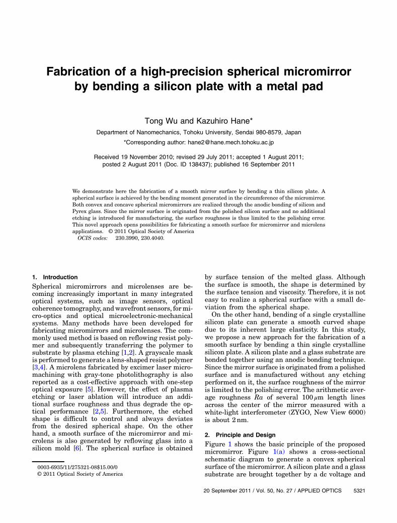
Figure 1 shows the basic principle of the proposedmicromirror. Figure 1(a) shows a cross-sectionalschematic diagram to generate a convex sphericalsurface of the micromirror. A silicon plate and a glasssubstrate are brought together by a dc voltage and
0003-6935/11/275321-08$15.00/0© 2011 Optical Society of America
20 September 2011 / Vol. 50, No. 27 / APPLIED OPTICS 5321
bonded using anodic bonding. The anode and cathodefor anodic bonding are set at the top side of the siliconwafer and the bottom side of the glass wafer, respec-tively. A metal pad with a semidiameter of a on theglass substrate is used to prevent the silicon platefrom bonding with the glass substrate. Thus, thesilicon plate is curved due to the bending momentgenerated by the electrostatic force generated by thedc voltage and the support force of the edge of themetal pad. When the surface of the silicon plate isput into contact with the glass surface outside themetal pad, anodic bonding begins and the siliconplate is fixed. As shown in the inset in Fig. 1(a), whenthe electrostatic force is increased, the bonding pointwill be closer to the edge of the metal pad. Since thesupport of the metal pad is rotation free, the siliconplate within the inner region of the edge of the metalpad (r ≤ a) only suffers a constant bending moment.
Figure 1(b) illustrates the schematic diagram forgenerating a concave spherical surface. A glass sub-strate is first etched to form a circular hole. Then ametal ring is deposited outside the circular holewith its diameter larger than that of the circularhole. The silicon plate will be forced to achieve a con-cave surface profile and become bonded with the ringpart of glass surface that lies outside the circular holebut inside the metal ring. The silicon plate within theinner region of the bonded ring part (r ≤ a) also suf-fers a constant moment. Therefore, in these twosituations, based on the strength of the materials[7], the equilibrium conditions of the silicon plate in-side the metal pad or the bonded ring part (r ≤ a)could be written as
8<:
ddr
n1rddr ðrϑÞ
o¼ 0;
ϑ ¼ −dzdr ;
ð1Þ
where z is the displacement of the plate, r refers tothe radial position from the center in the cylindrical
coordinate system as shown in Fig. 1, and ϑ is thedeflection angle. Solving the above differential equa-tion, we can get
rϑ ¼ 12C1r2 − C2; ð2Þ
z ¼ −14C1r2 − C2 ln rþ C3; ð3Þ
where C1, C2, and C3 are arbitrary constants.Using the boundary conditions that the deflection
angle ϑ equals zero at r ¼ 0 and the displacement zequals zero at r ¼ a, Eq. (3) can be solved as
z ¼ −C1
4ðr2 − a2Þ; ð4Þ
which suggests a parabolic surface of the circularmirror. In this calculation, single crystalline siliconis treated as an isotropic material for easy analysis.It should be noted that the above calculation is validprovided that the deflection z is small. Although theactual deflection under the application of a constantbending moment is considered to be spherical, thedeflection can be well expressed by a parabola underthe condition of a small deflection [8].
As shown in the inset in Fig. 1(a), the constant C1can be determined by another boundary conditionthat the first-order derivative of z at r ¼ a equalsthe tangent of the angle θ of the tangent line
dzdr
����r¼a
¼ −C1a2
¼ tan θ; ð5Þ
while tan θ can be calculated from the distance dbetween the bonding point and the edge of the metalpad and the height h of the metal pad. We can easilyconsider the situation that an upward concentratedforce is applied at the end of a cantilever with alength of d. As a result, the end of the cantilever isbent upward, the displacement of which is h. We caneasily get tan θ by solving the displacement equationof the cantilever and getting its first derivation basedon the strength of the materials, which is given by
tan θ ¼ −3h2d
: ð6Þ
Substituting Eq. (6) into Eq. (5), we can obtain
C1 ¼ 3hda
: ð7Þ
So we can obtain the displacement and the effectivefocal length of the mirror as
z ¼ −3h4da
ðr2 − a2Þ; ð8Þ
Fig. 1. (Color online) Schematic diagram of (a) convex sphericalmicromirror and its fabrication, (b) concave spherical micromirror.
5322 APPLIED OPTICS / Vol. 50, No. 27 / 20 September 2011

f ¼ d3h
a: ð9Þ
Because d is determined by the applied voltage in theanodic bonding process, f increases linearly with theincrease of a.
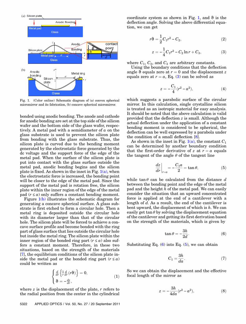
Based on this fabrication method, a more complexsurface can be generated by introducing anotherbonding region. For example, surfaces expressed byZernike polynomials, which are defined in a unit cir-cular aperture, could be generated. Zernike high-order spherical aberration mode Z22 notated by Noll[9], which is expressed by
Z22 ¼ffiffiffi7
pð20r6 − 30r4 þ 12r2 − 1Þ; ð10Þ
is plotted in Fig. 2(a), where r stands for the radiuscoordinate. Figure 2(b) shows the schematic diagramfor realizing this structure. The glass substrate isfirst etched to form a circular hole. Then, a metalpad with a diameter bigger than that of the circularhole is deposited. The center of the metal pad wasetched to form a small circular bonding region.The silicon plate is first bonded with the region out-side the metal pad and bent into a convex surfacewhen undergoing support at the circumference of themetal pad. Because an electrostatic force inside thehole of the glass substrate acts on it, the silicon plateinside the hole is bent into a concave surface andbonded at the small circular bonding region.
3. Fabrication Procedure
Figure 3(a) schematically illustrates the fabricationprocess of the freestanding silicon plate. The startingsilicon on insulator (SOI) wafer consists of a 10 μmsilicon device layer, a 1 μm buried oxide layer, anda 200 μm silicon handle layer. The silicon device layerwas first patterned and etched to form alignmentmarks for the subsequent anodic bonding process.Then the silicon handle layer was etched down to theburied oxide layer using deep reactive ion etching,where the buried oxide layer acted as an etching stoplayer. After removing the residual photo resist, theburied oxide layer was removed by buffered hydro-fluoric acid (BHF) etching.
The fabrication process of the glass chip is illu-strated in Fig. 3(b). First, a 500 μm thick Pyrex glass
(b)
-1
0
1-0.8 -0.6 -0.4 -0.2 0 0.2 0.4 0.6 0.8
-3
-2
-1
0
1
2(a)
y
x
Z22
(x, y
)
Fig. 2. (Color online) (a) High-order spherical aberration modesurface, (b) cross-sectional schematic of the high-order sphericalaberration mode mirror.
Fig. 3. (Color online) (a) Fabrication process of the silicon thin-plate mirror; (b) fabrication process of the glass chip for (I) convexmicromirror, (II) concave micromirror, and (III) high-order spheri-cal aberration surface; (c) schematic illustration of anodic bonding.
20 September 2011 / Vol. 50, No. 27 / APPLIED OPTICS 5323

substrate was patterned and etched by BHF to formthe desired structure, as shown in Figs. 1 and 2. Theetch depth is realized to be about 1:4 μm by control-ling the etching time. Then, a metal film with a thick-ness of ∼80nm (∼60nm thick gold layer and ∼20nmthick chrome adhesion layer) was sputtered on the
glass substrate and patterned to form the desiredmetal pads, while the top gold layer of the metalpad was also used as a guard to keep the silicon platefrom bonding with the glass substrate.
Finally, as shown in Fig. 3(c), the anodic bondingprocess was carried out to bond the front surface
Fig. 4. (Color online) (a) Surface profile of the fabricated silicon plate with initial deflection, (b) surface profile of the fabricated siliconplate across the center.
Fig. 5. (Color online) (a) Surface profile of the fabricated convex micromirror expressed by a contour map, (b) height profile of the convexmicromirror surface, (c) measured surface profile and fitted parabola, (d) residual errors deviating from the fitted parabola.
5324 APPLIED OPTICS / Vol. 50, No. 27 / 20 September 2011

of the silicon device layer and the glass substrate. Inthis process, the electrostatic force is utilized to bringthe silicon and the Pyrex glass into contact so theanodic bonding can proceed. If the electrostatic force
is too small, the anodic bonding may be incompletewith some undesirable voids. On the other hand, ifthe electrostatic force is too large, we will find thatour devices are always broken, as the thin silicon
Fig. 6. (Color online) Focal length of the fabricated convex micromirror as a function of the diameter.
Fig. 7. (Color online) (a) Surface profile of the fabricated concavemicromirror expressed by a contourmap, (b) height profile of the concavemicromirror surface, (c) measured surface profile and fitted parabola, (d) residual errors deviating from the fitted parabola.
20 September 2011 / Vol. 50, No. 27 / APPLIED OPTICS 5325

plate cannot bear too large a load. In the experiment,the electrostatic force is adjusted by changing theapplied voltage in the bonding process. We did someexperiments and found the best voltage range to be900–1000 V. The bonding process was practically car-ried out at the temperature of 400 °C and the voltageof 1000V with voltage ramping in four steps (400,600, 800, and 1000V) to avoid current peaks, whichmay produce electric discharges inducing bondingdefects or even device damage [10].
4. Results and Discussion
The initial deformation of the silicon plate is mea-sured with the turned SOI wafers from the siliconhandle layer side with ZYGO. As shown in Fig. 4,the surface deflection is slightly downward due tothe residual stress induced by the release of the sili-con dioxide layer, and the peak-to-valley value ismeasured at ∼0:12 μm for a 1200 μm diameter siliconplate. As the front side of the device layer of the SOIwafer is finally bonded with the glass substrate,
Fig. 8. (Color online) (a) Optical micrograph of the glass chip, (b) height profile of the glass chip surface, (c) surface profile of the fabricatedhigh-order polynomial surface expressed by a contour map, (d) height profile of the fabricated high-order polynomial surface, (e) measuredsurface profile and the fitted sixth-order polynomial curve, (f) residual errors deviating from the fitted sixth-order polynomial curve.
5326 APPLIED OPTICS / Vol. 50, No. 27 / 20 September 2011

there is a ∼120nm cuplike deformation within thebonding process.
The deformation of the fabricated convex mirrorwas measured with the interferometer. The diameterof the Si plate is 1200 μm. The metal pad is 1000 μmin diameter and ∼80nm thick. Figure 5 shows themeasured results. Figure 5(a) shows the height dis-tribution expressed by a contour map. Figure 5(b)shows the height profile of the mirror surface. Theheight difference between the center and the edge ofthe mirror is about 1:8 μm. The surface profile isplotted as a solid curve in Fig. 5(c). The surface pro-file of the region inside the metal pad is fitted bysecond-order polynomial fitting, and the fitted parab-ola is shown as a dashed curve in Fig. 5(c) with theresidual error plotted in Fig. 5(d). The rms errordeviating from the fitted parabolic curve equals25:96nm in a 1000 μm diameter circular area. Thefocal length of the micromirror is 32:4mm, which isextracted from the measured profile.
Mirrors with different diameters are also fabri-cated by changing the diameter of themetal pad from100 to 1000 μm. The corresponding focal length of themicromirrors is extracted from the measured profileand changes from 5.5 to 32:5mm, as shown in Fig. 6.The measurement results show that the focal lengthincreases linearly with the increase of the diameter.Furthermore, the distance d in Eq. (9) is measured tobe 16 μm from the backside micrograph of the fabri-cated mirror. Substituting the value of d andhð80nmÞ into Eq. (9), we can derive the theoreticalprediction of the focal length f as f ¼ 66:7a ðμmÞ,where a is the radius of the metal pad. The plot ofthe theoretically calculated f is shown as the dashedcurve in Fig. 6, which indicates a slightly larger slopethan that of the experimental results. The surface ofthe fabricated concave micromirror is measured bythe interferometer. The diameter of the silicon thinplate is 1200 μm. The metal ring on the glass chiphas an outside diameter of 1100 μm and an insidediameter of 1000 μm. The diameter of the hole insidethe metal ring is 800 μm. Figure 7(a) shows theheight distribution expressed by a contour map.Figure 7(b) illustrates the height profile of the mirrorsurface. The surface profile across the center of themirror is plotted as a solid curve in Fig. 7(c). The sur-face profile of the region inside the circumstance ofthe hole is fitted by a second-order polynomial,and the fitted parabola is shown as the dashed curvein Fig. 7(c) with the residual error plotted in Fig. 7(d).The rms error deviating from the fitted paraboliccurve equals 13:03nm in an 800 μm diameter cir-cular area. The focal length of the micromirroris 118:5mm.
These results indicate that our proposed method issimple and feasible for generating a parabolic sur-face with different desired focal lengths and aper-tures. First, in order to get the desired aperture,the value of a, which is illustrated in Fig. 1, can bemodified. Second, as expressed by Eq. (9), the focallength f relates to the distance d and the thickness
of the metal pad h, where d can be changed experi-mentally by adjusting the applied voltage in the ano-dic bonding process and h can be easily controlled inthe metal deposition process.
The fabricated glass substrate for the high-orderspherical aberration surface expressed by Eq. (10)is shown in Fig. 8(a), and the height profile is illu-strated in Fig. 8(b). The dimension of the etched holeof the glass chip is 1:3 μm in height and 1000 μm indiameter. The metal pad is about 80nm thick and1100 μm in diameter, which is 100 μm larger thanthat of the hole of the glass chip. The circular bondingregion at the center of the hole is 100 μm in diameter.Figure 8(c) shows the height distribution expressedby a contour map of the fabricated mirror surface.Figure 8(d) illustrates the height profile of the mirrorsurface. The surface profile is plotted as a solid curvein Fig. 8(e). The surface profile in the region insidethe metal pad is fitted by a sixth-order polynomialfitting. The fitted sixth-order polynomial givenby Z ¼ 2:57 � ffiffiffi
7p ð20r6 − 14:24r4 þ 2:78r2Þ − 0:79 is
plotted in Fig. 8(e), where Z represents the heightand r represents the position. The residual error isplotted in Fig. 8(f). The rms error deviating from thefitted sixth-order polynomial curve equals 33:61nmin a 1200 μm diameter circular area.
The surface roughness of the fabricated micro-mirrors is obtained from the ZYGO data by measur-ing the arithmetic average roughness Ra of several100 μm length lines across the center of the mirror.The average value is 2nm.
5. Conclusion
A fabrication method for bending a silicon thin platefor generating a smooth mirror surface was proposedand experimentally demonstrated. Convex micromir-rors with diameters from 100 to 1000 μm were fabri-cated, the focal lengths of which were from 5.5 to32:5mm. An 800 μm diameter concave micromirrorwas also fabricated. The surface profiles of the fabri-cated spherical mirrors were well fitted with a para-bolic curve. Extremely low-roughness surfaces wereguaranteed by a nonetching process for the surfacegeneration.Moreover, the high-order spherical aberra-tion surface expressed by Zernike polynomials Z22was generated by modifying the bonding region.From these experimental results, the proposed meth-od is useful for generating smooth spherical surfaceswith desired focal lengths and apertures and evenmore complex surfaces expressed by high-orderpolynomials.
The authors would like to thank T. Kuriyagawa forthe interferometricmeasurement andY. Kanamori forhis advice on the experiment. This work is supportedby the Japan Society for the Promotion of Science.
References1. H. P. Herzig, Micro-optics (Taylor & Francis, 1997).2. S. Audran, B. Faure, B. Mortini, J. Regolini, G. Schlatter,
and G. Hadziioannou, “Study of mechanisms involved in
20 September 2011 / Vol. 50, No. 27 / APPLIED OPTICS 5327

photoresist microlens formation,” Microelectron. Eng. 83,1087–1090 (2006).
3. G. Wang, S. Wang, and C. Chin, “Fabrication andmolding of gray-scale mask based aspheric refractionmicrolens array,” JSME Int. J., Ser. C 46, 1598–1603(2003).
4. K. Totsu and M. Esashi, “Gray-scale photolithography usingmaskless exposure system,” J. Vac. Sci. Technol. B 23,1487–1490 (2005).
5. C.-H. Tien Y.-E. Chien, Y. Chiu, and H.-P. D. Shieh, “Microlensarray fabricated by excimer laser micromachining with gray-tone photolithography,” Jpn. J. Appl. Phys. 42, 1280–1283(2003).
6. P. Merz, H. J. Quenzer, H. Bernt, B. Wagner, and M. Zoberbier,“A novel micromachining technology for structuring borosili-cate glass substrates,” in Proceedings of IEEE Conference
on Solid State Sensors, Actuators and Microsystems (IEEE,2003), pp. 258–261.
7. S. Timoshenko, Strength of Materials II (Van NostrandReinhold, 1953).
8. H. Conrad, T. Klose, T. Sander, H. Schenk, and H. Lakner,“Actuating methods of quasistatic micromirrors for activefocus variation,” in Proceedings of International Studentsand Young Scientists Workshop, Photonics and Microsystems(IEEE, 2008), pp. 7–11.
9. R. J. Noll, “Zernike polynomials and atmospheric turbulence,”J. Opt. Soc. Am. 66, 207–211 (1976).
10. V. Dragoi, P. Lindner, T. Glinsner, M. Wimplinger, and S.Farrens, “Advanced anodic bonding processes for MEMSapplications,” in Proceedings of Materials Research SocietySymposium (Materials Research Society, 2004), Vol. 782,pp. A5.80.1–A5.80.6.
5328 APPLIED OPTICS / Vol. 50, No. 27 / 20 September 2011