Embed Size (px)
Citation preview

FABRICATION AND PROPERTIES OF SILICA-EPOXY THIN FILM COMPOSITE
FOO YIN LIN EVON
UNIVERSITI SAINS MALAYSIA
2012
brought to you by COREView metadata, citation and similar papers at core.ac.uk
provided by Repository@USM
FABRICATION AND PROPERTIES OF SILICA-EPOXY THIN FILM COMPOSITE
by
FOO YIN LIN EVON
Thesis submitted in fulfillment of the requirements
for the Degree of
Master of Science
JUNE 2012

�
ŝŝ��
DECLARATION
I hereby declare that I have conducted, completed the research work and written the
dissertation entitled Fabrication and Properties of Silica-Epoxy Thin Film
Composite . I also declare that it has not been previously submitted for the award of
any degree or diploma or other similar title of this for any other examining body or
University.
Saya isytiharkan bahawa kandungan yang dibentangkan di dalam disertasi bertajuk
Fabrikasi dan Sifat-Sifat Komposit Filem Nipis Silika-Epoksi ini adalah hasil
kerja saya sendiri dan telah dijalankan di Universiti Sains Malaysia kecuali
dimaklumkan sebaliknya. Disertasi ini juga tidak pernah disertakan untuk ijazah
yang lain sebelum ini.
Signature: __________________
Name of Student: Foo Yin Lin Evon
Date: 30/01/2012
Witness by,
Signature: __________________
Supervisor: Assoc. Prof. IR. Dr. Mariatti Jaafar
Date: 30/01/2012

ŝŝŝ��
ACKNOWLEDGEMENT
Upon completion of this thesis, I would like to grab the opportunity to express
my deepest gratittude towards my family members; father Foo Chee Boo, mother Choo
Chooi Hiang, brother Foo Siang Min Aaron and sister Foo Ching Lin Evelyn. Their
undivided morale support throughout my research work has propelled me to
perform even better.
I would also like to thank my dedicated and supportive main supervisor,
Associate Professor IR Dr Mariatti Jaafar for all the help provided. She has guided me
towards the right direction many times in all aspect, from data analysis to publishing
journals.
Next would be my co-supervisor, Associate Professor Dr Azizan Aziz. Thank
you for constantly reviewing my journals and thesis. Special thanks to Associate
Professor Dr Zulkifli b. Ahmad for teaching and guiding me during the data analysis
period. All assistance provided is not forgotten.
Apart from the supervisors at Universiti Sains Malaysia (USM), there is another
Here, I would like to thank Dr Sim Lim Chong for constantly acknowleging my works
and giving positive feedback on improving the research works. At the same time, I wish
to acknowlege the contribution and sponsorship of Intel Technology (M) Sdn. Bhd. for
rewarding me the Intel Fellowship 2009-2011 and Intel Research Grant 2009-2011 (No:
6050175) in order to carry out this research works.

ŝǀ��
Lastly, my appreciation goes towards Universiti Sains Malaysia (USM),
especially School of Materials and Mineral Resources Engineering (SMMRE) for
providing a proper environment to complete my research studies. USM had also
allocated a Postgraduate Research University Grant (No: 8043020) for me to carry out
these works. Besides that, I would also like to thank the Dean of SMMRE, Professor
Ahmad Fauzi b. Mohd Noor, all administrative and technicians for providing assistance
during my research.

ǀ��
TABLE OF CONTENTS
DECLARATION ii
ACKNOWLEDGEMENTS iii
TABLE OF CONTENTS v
LIST OF TABLES x
LIST OF FIGURES xii
LIST OF ABBREVIATIONS xviii
LIST OF SYMBOLS xix
ABSTRAK xx
ABSTRACT xxii
CHAPTER 1 INTRODUCTION
1.1 Background 1
1.2 Problem Statements 2
1.3 Objectives 5
1.4 Summary of the Thesis 5
CHAPTER 2 LITERATURE REVIEW
2.1 Electronic Packaging
2.1.1 Introduction
2.1.2 Polymer in Electronic Packaging
2.1.2.1 Epoxy
2.1.2.2 Curing Agents
7
7
9
13
15
2.2 Polymer Composite in Electronic Packaging
2.2.1 Introduction
23
23

ǀŝ��
2.2.2 Factors Influence Polymer Composite
2.2.2.1 Type of Fillers
2.2.2.2 Volume Fraction or Loading of Fillers
2.2.2.3 Shape and Size of Fillers
2.2.2.4 Surface Treatment of the Fillers
2.2.3 Application of Polymer Composite in Electronic
Packaging Underfill and Molding Compound
24
24
26
27
28
31
2.3 Polymer Thin Film in Electronic Packaging
2.3.1 Introduction
2.3.2 Properties between Bulk and Thin Polymeric
Materials
2.3.3 Application of Polymer Thin Film
2.3.3.1 Flexible Circuit Technology
Flexible Circuit Board
2.3.4 Fabrication of Thin Film
2.3.4.1 Conventional Thin Film Fabrication
Methods
2.3.4.2 Spin Coating
33
33
35
35
37
37
39
2.4 Current Research on Polymer Composite Thin Film 41
CHAPTER 3 EXPERIMENTAL
3.1 Raw Materials
3.1.1 Epoxy Resin
3.1.2 Curing Agents
3.1.3 Silica Fillers
44
44
45
46

ǀŝŝ��
3.1.4 Silane Coupling Agent 46
3.2 Methodology
3.2.1 Fabrication of Thin Film Composite with Micron
and Nano-sized Silica Filler
3.2.2 Comparison between Polyetheramine based
Curing Agent and Imidazole Derivatives Curing
Agent.
3.2.3 Surface Treatment of n-Si
47
47
49
50
3.3 Characterization
3.3.1 Particle Size Analysis
3.3.2 Morphology
3.3.3 Specific Surface Area
3.3.4 Tensile Properties
3.3.5 Thermal Properties
3.3.5.1 Dynamic Mechanical Properties
(DMA)
3.3.5.2 Coefficient of Thermal Expansion
(CTE)
3.3.5.3 Thermogravimetric Analysis (TGA)
3.3.6 Dielectric Properties
3.3.7 Moisture Absorption
53
53
53
54
55
55
55
56
56
57
58
3.3.8 Fourier Transform InfraRed Spectroscopy (FTIR)
58

ǀŝŝŝ��
CHAPTER 4 RESULTS AND DISCUSSION
4.1 Fabrication of Thin Film Composites with Micron and
Nano-sized Silica Filler
4.1.1 Introduction
4.1.2 Tensile Properties
4.1.3 Dynamic Mechanical Properties
4.1.4 Coefficient of Thermal Expansion (CTE)
4.1.5 Thermo Gravimetric Analysis (TGA)
4.1.6 Moisture Absorption
4.1.7 Dielectric Properties
59
59
59
73
77
79
82
84
4.2 Comparison Between Polyetheramine Based Curing
Agent and Imidazole Derivatives Curing Agent
4.2.1 Introduction
4.2.2 Tensile Properties
4.2.3 Dynamic Mechanical Properties
4.2.4 Coefficient of Thermal Expansion (CTE)
4.2.5 Thermogravimetric Analysis (TGA)
4.2.6 Moisture Absorption
87
87
87
96
101
102
105
4.3 Surface Treatment of n-Si
4.3.1 Introduction
4.3.2 Tensile Properties
4.3.3 Dynamic Mechanical Properties
4.3.4 Coefficient of Thermal Expansion (CTE)
4.3.5 Thermogravimetric Analysis (TGA)
4.3.6 Moisture Absorption
107
107
107
116
119
120
122
ŝdž��
CHAPTER 5 CONCLUSION & FUTURE WORK
RECOMMENDATION
5.1 Conclusion 125
5.2 Recommendation for Future Works 127
REFERENCES 129
LIST OF PUBLICATIONS 143

dž��
LIST OF TABLES
Table No. Description Page
Table 1.1 Typical CTE of electronic packaging materials (Minges &
ASM International Handbook Committee, 1989; Suhir et al.,
2007; Hodgin & Estes, 1999)
3
Table 2.1 Characteristic and applications for the common type of
thermoset and thermoplastic materials used in electronic
industry (Harper, 2005).
11
Table 2.2 Types of flexible circuit construction, the features and
application requirements (Jawitz, 1997; Gilleo, 1992).
37
Table 2.3 Comparison of thin film fabrication methods (Nan, 2006;
40
Table 3.1 Samples name, formulation and curing profile for the
preparation of two different types of epoxy/n-Si thin films.
50
Table 3.2 Samples name, treatment time and curing profile for the
preparation of two different types of epoxy/n-Si thin films.
53
Table 4.1 Area under stress-strain curve derived from Figure 4.1. 61
Table 4.2 Specific surface area (SSA), calculated values of nearest
neighbour spacing (dn) and epoxy/filler interface area per
volume unit ( ) for both -Si and n-Si. The dn and
were determined using Equation 3.2 and 3.3 according to the
lowest and highest amount of filler used for each thin film
composite samples.
71
Table 4.3 Coefficient of thermal expansion (CTE) for neat epoxy thin
film and selective loading of -Si and n-Si thin film
79

džŝ��
composites.
Table 4.4 Initial decomposition temperature (IDT) and temperature at
maximum rate of weight loss (Tmax) for neat epoxy thin film
and different loading of -Si and n-Si thin film composites.
82
Table 4.5 Coefficient of thermal expansion (CTE) for polyetheramine n-
Si and imidazole n-Si thin film composites with different
loading of n-Si.
102
Table 4.6 Initial decomposition temperature (IDT) and temperature at the
maximum rate of weight loss (Tmax) for polyetheramine and
imidazole thin films with different loading of n-Si.
105
Table 4.7 Identification of the FTIR spectrum frequency observed in
treated polyetheramine and imidazole cured n-Si thin film
composites (Motawie et al. 2010).
113
Table 4.8 Coefficient of thermal expansion (CTE) for untreated (A-8
wt% and Im-8 wt%) and treated (A-8H and Im-8H) thin film
composites.
120
Table 4.9 Initial decomposition temperature (IDT) and temperature at the
maximum rate of weight loss (Tmax) for untreated (A-8 wt%
and Im-8 wt%) and treated (A-8H and Im-8H) thin film
composites.
122

džŝŝ��
LIST OF FIGURES
Table No. Description Page
Figure 2.1 Typical hierarchy of electronic packaging (Chung, 1995). 9
Figure 2.2 Categories of epoxy resins (Dunn, 2003; Mays &
Hutchinson, 1992).
14
Figure 2.3 Chemical structure for (a) DGEBA and (b) DGEBF (Mays
& Hutchinson, 1992; Balachandran, 2000)
15
Figure 2.4 Categories of curing agents 17
Figure 2.5 Curing mechanism of epoxy by amine curing agents
(Licari & Swanson, 2011)
18
Figure 2.6 Curing mechanism of epoxy by anhydride curing agents
(Licari & Swanson, 2011)
19
Figure 2.7 Types of alicyclic anhydrides commonly used with epoxy
resin (Lubin & Peters, 1998).
20
Figure 2.8 Polymerization reaction of epoxy by Lewis bases (a) ring
opening, (b) cross-linking (Licari & Swanson, 2011).
21
Figure 2.9 Curing mechanism of epoxy by imidazoles (Omrani et al.,
2008).
22
Figure 2.10 Schematic of chemical surface modification by silane
coupling agent (Sun et al., 2005b).
30
Figure 2.11 Integrated circuit packaging by wire-bonded and flip-chip
technology.
32
Figure 2.12 The comparison of chain segments for polymer bulk and
thin film (Karim & Kumar, 2000).
34
Figure 2.13 Representative example of basic and selected flexible 36

džŝŝŝ��
circuit construction (Fjelstad, 2006).
Figure 2.14 Stages of spin coating process: Deposition of polymer
solution, spin-up and stable fluid outflow.
41
Figure 3.1 Chemical structure for (a) EPON 8281 (DGEBA) and (b)
EPO-TEK 323LP (DGEBF) (Ghaemy & Riahi, 1996).
44-45
Figure 3.2 Chemical structure for EC 301 (polyetheramine based
curing agent) and imidazole (www.basf.de; Omrani et al.,
2008).
45
Figure 3.3 Chemical structure for (3-Glycidyloxypropyl)
trimethoxysilane (Xie et al., 2011).
46
Figure 3.4 Flow chart for the fabrication of thin film composites for
Section 3.2.1 to 3.2.3.
48
Figure 3.5 Treatment process for n-Si in the epoxy system. 52
Figure 4.1 Stress versus strain curve for thin film composites with
selective loading of -Si (5 wt% and 30 wt%) and n-Si (1
wt% and 8 wt%) fillers.
60
Figure 4.2 Schematic drawing of the toughening mechanisms by (a)
crack pinning, and (b) crack deflection in the inorganic
filled composite (Zhao & Rensselaer, 2007; Liang, 2008).
62
Figure 4.3 Cross-section view of the tensile fracture surface for (a)
neat epoxy thin film (magnification used is 150×), (b) 5
wt% -Si thin film composites (magnification used is
500×), (c) 30 wt% -Si thin film composites
(magnification used is 2000×), (d) 1wt% n-Si thin film
composites composites (magnification used is 500×), (e)
63-65

džŝǀ��
8wt% n-Si thin film composites (magnification used is
1000×)
(magnification used for all the enlarged images are 5000×)
Figure 4.4 Tensile modulus and strength for thin film composites with
different loading of -Si (5 wt% to 30 wt% and n-Si (1
wt% to 8 wt%) fillers.
67
Figure 4.5 Particle size distribution for (a) -Si that determined by
HELOS Particle Size Analyzer WINDOX 5, (b) n-Si that
determined by MALVERN Zeta Sizer Nano-Series.
68-69
Figure 4.6 (a) SEM image for -Si, (b) SEM image for n-Si and (c)
TEM image for n-Si.
(magnification used are 50000× for (a), (b) and 35000×
for (c))
69
Figure 4.7 SEM image of tensile fracture surface for thin film
composite with (a) 0 wt% or neat epoxy (b) 1 wt% n-Si, (c)
8 wt% n-Si, (d) 5 wt% µ-Si, (e) 30 wt% -Si.
(Magnification used are 2500× for (a), 30000× for (b), (c)
and 5000× for (d), (e))
72-73
Figure 4.8 Storage modulus for neat epoxy thin film and thin film
composites with the lowest and highest loading of -Si (5
wt% and 30 wt%) and n-Si (1wt% and 8 wt%) fillers.
74
Figure 4.9 Tan for neat epoxy thin film and thin film composites
with lowest and highest loadings of -Si (5 wt% and 30
wt%) and n-Si (1wt% and 8 wt%) fillers.
77
Figure 4.10 (a) TGA thermogram and (b) DTG curve for neat epoxy 81

džǀ��
and thin film composites with selective loading of -Si (5
wt%, 15 wt% and 30 wt%) and n-Si (1wt%, 2 wt% and 8
wt%) fillers.
Figure 4.11 Moisture uptake for the neat epoxy, selected loading of -
Si and n-Si thin film composite over 19 hours.
83
Figure 4.12 Dielectric Constant ( ) for standard sample and after
moisture absorption of neat epoxy thin film, selected
loading of -Si and n-Si thin film composites.
86
Figure 4.13 Stress-strain curve (a) for the selective n-Si loading of
polyetheramine and imidazole cured thin film composites,
(b) of 5 tensile specimens for each A-0 wt% and A-2 wt%
samples.
89
Figure 4.14 SEM images of the tensile fracture surface for (a) A-0 wt%
(b) Im-0 wt%, (c) A-2 wt% where the arrow pointers
indicate crack pinning, (d) Im-2 wt%, (e) A-8 wt% and (f)
Im-8 wt%
(All SEM images are taken at 10000× magnification)
90
Figure 4.15 Proposed cross-linking reaction mechanism of (a)
EPOTEK 323LP with imidazole curing agent and (b)
EPON 8281 with polyetheramine curing agent (Ham et al.,
2010)
91-92
Figure 4.16 FTIR spectrum for A-8 wt% and Im-8 wt% thin films. 94
Figure 4.17 Tensile modulus and tensile strength for polyetheramine n-
Si thin films and imidazole n-Si thin films with different
loading of n-Si.
95
džǀŝ��
Figure 4.18 for polyetheramine n-Si and
imidazole cured n-Si thin films composites with selective
loading of n-Si.
97
Figure 4.19 Tan for polyetheramine n-Si and imidazole n-Si thin film
composites with different loading of n-Si.
99
Figure 4.20 SEM images of the cross section (a) Im-2 wt% with arrow
pointers indicate the voids presence, (b) Im-8 wt% of thin
film composites.
(Magnification used is 30000×)
100
Figure 4.21 (a) TGA thermogram and (b) DTG curve for the
polyetheramine and imidazole thin films with different
loading of n-Si.
104
Figure 4.22 Moisture uptake for polyetheramine and imidazole thin
film composite with different loading of n-Si over 19
hours.
106
Figure 4.23 Stress versus strain curve for polyetheramine and
imidazole thin film with untreated and treated 8 wt% n-Si
under different treatment time.
108
Figure 4.24 Schematic of propose chemical reaction and structure for
the (a) hydrolysis of silane coupling agent, (b)
condensation of silane coupling agent, (c) condensation for
short treatment time, (d) condensation for longer treatment
time, (e) cross-linked structure for polyetheramine thin
film composites with treated n-Si.
109-110
Figure 4.25 FTIR spectrum for (a) polyetheramine thin film composites 112

džǀŝŝ��
with untreated (A-8 wt% untreated) and treated n-Si under
treatment period of 8 hours (A-8H), 16 hours (A-16H) and
24 hours (A-24H), (b) untreated imidazole cured n-Si thin
film composites (Im-8wt% non-treated) and those treated
under 8H (Im-8H), 16H (Im-16H) and 24H (Im-24H).
Figure 4.26 Tensile modulus and strength for 8 wt% n-Si filled EPON
and EPOTEK thin film composites with different treatment
time.
115
Figure 4.27 SEM image of tensile fracture surface for (a) A-8 wt%
(untreated) (b) Im-8 wt% (untreated), (c) A-8H, (d) Im-8H
treated thin film composites.
(SEM magnification, ×30000)
115-116
Figure 4.28 Storage modulus for non-treated (A-8 wt% and Im-8 wt%)
and treated (A-8H and Im-8H) thin film composites.
117
Figure 4.29 Tan for untreated (A-8 wt% and Im-8 wt%) and treated
(A-8H and Im-8H) thin film composites.
118
Figure 4.30 (a) TGA thermogram and (b) DTG curve for untreated (A-
8 wt% and Im-8 wt%) and treated (A-8H and Im-8H) thin
film composites.
121
Figure 4.25 Moisture uptake for untreated (A-8 wt% and Im-8 wt%)
and treated (A-8H and Im-8H) thin film composites over
19 hours.
124

�
džǀŝŝŝ��
LIST OF ABBREVIATIONS
mm
SSA
milimetre
specific surface area
CTE Coefficient of thermal expansion
DMA
TMA
SEM
TEM
FTIR
TGA
DTG
IDT
Dynamic mechanical analysis
Thermal mechanical analysis
Scanning Electron Microscope
Transmission Electron Microscope
Fourier Transform InfraRed Spectroscopy
Thermo Gravimetric Analysis
Derivative Thermo Gravimetric
initial decomposition temperature
GPa Giga pascal (109 Pa)
H hour
ppm Part per million
M Molarity
ml mililiter
min minutes
MPa Mega pascal (106 Pa)
mm milimeter
s second
T Temperature
džŝdž��
LIST OF SYMBOLS
oC Degree Celsius
% Percentage
µm
nm
Micrometer (10-6 m)
Nanometer (10-9 m)
E
TS
B
Storage Modulus
Tensile Modulus
Tensile Strength
Strain at Break
Tg Glass Transition Temperature
Tmax temperature at the maximum rate of weight loss
G
R
D
IA/V
Tan Delta
Coefficient of Thermal Expansion at glassy region
Coefficient of Thermal Expansion at rubbery region
Mean particle size
interface area between the epoxy and filler per volume unit

dždž��
FABRIKASI DAN SIFAT-SIFAT KOMPOSIT FILEM NIPIS SILIKA-EPOKSI
ABSTRAK
Dengan peningkatan minat terhadap pembungkusan elektronik berketumpatan
tinggi, penskalaan dimensi menjadi kunci terhadap evolusi ini. Dalam kajian ini,
komposit filem nipis epoksi dengan pengisi silika dihasilkan menggunakan proses
salutan putaran. Dalam bahagian pertama penyelidikan ini, perbandingan sifat-sifat
mekanik dan terma bagi komposit filem nipis yang mengunakan pengisi mikro-silika
(µ-Si) dan nano-silika (n-Si) telah dijalankan. Komposit filem nipis dengan
pembebanan n-Si yang rendah didapati mencapai sifat-sifat tegangan dan terma yang
setara dengan komposit filem nipis yang mengandungi pembebanan µ-Si yang tinggi.
Dengan nisbah luas permukaan dan isipadu yang tinggi, n-Si dengan pecahan berat
rendah menunjukkan kemampuannya dalam mencapai prestasi yang setara dengan µ-Si.
Dari segi agen pematangan, komposit filem nipis yang dimatangkan dengan imidazol
didapati mempunyai sifat-sifat mekanik dan terma yang baik hasil daripada kehadiran
lima anggota gelang dalam struktur kimia imidazol. Penyerapan lembapan bagi sampel
yang dimatangkan dengan imidazol didapati lebih tinggi daripada sampel yang
dimatangkan oleh polieteramin kerana resin yang telah dimatangkan dengan imidazol
menjadi resin yang lebih berkutub. Serakan bagi pengisi n-Si didapati bertambah baik
melalui rawatan n-Si dengan agen gandingan (3-Glycidyloxypropyl) trimethoxysilane.
Adalah didapati bahawa rawatan n-Si dengan agen gandingan (3-Glycidyloxypropyl)
trimethoxysilane selama 8 jam menghasilkan sifat-sifat mekanik komposit filem nipis
yang optimum. Masa rawatan yang panjang menyebabkan penurunan nilai modulus
tegangan dan kekuatan tegangan tetapi menaikkan kebolehlenturan komposit filem nipis.

dždžŝ��
Kewujudan n-Si yang dirawat dalam sistem komposit menyebabkan peningkatan nilai
pekali pengembangan terma (CTE) dan merendahkan kestabilan terma. Walau
bagaimanapun, rawatan n-Si adalah didapati menyebabkan pengubahsuaian permukaan
n-Si yang hidrofilik kepada permukaan yang hindar air, ini mengurangkan penyerapan
lembapan pada komposit filem nipis.

dždžŝŝ��
FABRICATION AND PROPERTIES OF SILICA-EPOXY THIN FILM
COMPOSITE
ABSTRACT
With the increasing interest in high density electronics packaging, dimensional
scaling becomes the key to evolution. In this study, epoxy thin film composites with
silica fillers were fabricated using spin coating process. In the first part of this research,
the mechanical and thermal properties of the thin film composites using micron-silica
(µ-Si) and nano-silica (n-Si) fillers were compared. Low loading of n-Si thin film
composites was found to have the ability to achieve equivalent tensile and thermal
properties compared to the highly loaded µ-Si thin film composite. With higher surface
area to volume ratio, n-Si shows its capability to achieve a substantial performance with
-Si. In terms of curing agents, imidazole cured
thin film was found to have better mechanical and thermal properties due to the presence
of five membered ring in the imidazole chemical structure. The moisture absorption of
the imidazole cured samples were slightly higher than the polyetheramine cured samples
because imidazole cured resin is a polar resin. The dispersion of the n-Si filler was
improved by the treatment of n-Si with (3-Glycidyloxypropyl) trimethoxysilane
coupling agent. It was observed that 8 hours treatment time showed high mechanical
properties of the thin film composites. Prolong treatment time caused the drop in tensile
modulus and tensile strength but increase the flexibility of the thin film composites. The
presence of treated n-Si in the composite system causes the increase in the coefficient of
thermal expansion (CTE) value and lowers the thermal stability compared to the
untreated n-Si thin film composites. However, treatment of the n-Si was found to cause

dždžŝŝŝ��
the modification of the hydrophilic n-Si surface into a hydrophobic surface, thus reduced
the moisture absorption of the thin film composites.

1
CHAPTER 1
INTRODUCTION
1.1 Background
In line with the miniaturization trend, the evolution of the traditional
integrated circuit (IC) packaging had taken place from wire-bonded silicon chip on
lead frame into flip chip packaging. This high electronic packing density gave
smaller, cheaper and lighter assemblies with improved microprocessor performance
(He et al., 2000). With the continuous improvement of the microprocessor
performance, dimensional scaling of the electronic packaging materials becomes the
key of evolution other than the circuit design and materials selection. Hence, the
trend of the electronics design has now shifted to flexible electronics technology,
Thickness and flexibility are the major
concern in flexible electronic technology. Therefore, polymer materials are
promoted as the main choice in the materials selection for thin film package
fabrication.
Thin film is the size reduction of bulk materials in one dimension. According
to ASTM D 882-02, a material is known as thin film when the thickness is less than
0.25 mm. Thin films of polymers are getting acceptance for technological
applications ranging from multicolor photographic printing to paints, adhesives,
index-matched optical coatings, photoresists and low dielectric electronic packaging
(Ade et al., 1998). In comparison to bulk properties, much less is known about the
properties of polymers when they are processed into thin films. Typically, the
polymer-substrate and polymer-air interfacial energies or kinetic barriers play
important roles in determining the morphology and dynamics in thin films.

2
1.2 Problem Statements
Polyester and polyimide are the most common materials used in flexible
electronic (Coombs, 2001 de was favorable as the
solution to the temperature limits of polyester. The low coefficient of thermal
expansion (CTE) and ability to retain its electrical and mechanical properties over
wide range of temperature (as high as 400oC) had made it become the favorable
choice of materials used in electronic packaging (Minges & ASM International
Handbook Committee, 1989). However, the cost ratio of polyimide to polyester is
approximately 20:1 (Gilleo, 1997). Comparing with epoxy resins, polyimide cost
twice or thrice higher. Besides, the fast moisture uptake of polyimide causes huge
changes in the electrical properties that subsequently limit its development for the
electronic industry (Kamei et al., 2000). In terms of fabrication, polyimides are
difficult to work with, especially in multi-layer processing. Extra precaution steps
have to be taken when drilling and routing which are required in the fabrication
process. This is because polyimide materials have lower inter-laminar bond strength
than epoxy systems (www.ami.ac.uk).
Epoxy resins are commonly used in electronic packaging due to their good
chemical, mechanical and electrical properties. Although epoxy resin covers a range
of materials with widely differing characteristics and costs, but a multifunctional
materials/blends of epoxy resins can be developed to fill the niche between lower-
cost regular epoxies and high-performance resins, and give an extended operational
temperature range at lower cost than polyimide (Coombs, 2001). The properties of
the epoxy film can be easily altered through the selection of fillers and curing agents.
Understanding on the resin network formation through the application of different

3
curing agents is necessary since the properties of cured epoxy are dependent on the
chemical structure and the degree of crosslinking of resin network (Buist et al.,
1994). However, the poor thermal properties of the epoxy resin such as high CTE
causes the warpage failure in the electronic packaging. Table 1.1 shows the CTE of
epoxies and other materials used in electronic packaging. The large differences in
CTE raise the issue of thermal mismatch between the silicon chip and the flexible
epoxy substrate. Residual warpage takes place with the presence of thermal cycling
which leads to the mechanical constraints of solder joint attached on the substrate.
Subsequently, this also causes the cracking and delamination problem on the
package (Bruce, 2007; Valdevit et al., 2008). In order to enhance the thermal
stability of the epoxy based packaging, many efforts such as incorporation of
inorganic filler into the underfill were studied (He et al., 2000; Lee et al., 2007; Lee
et al., 2005).
Table 1.1. Typical CTE of electronic packaging materials (Minges & ASM International Handbook Committee, 1989; Suhir et al., 2007; Hodgin & Estes, 1999)
Materials CTE (ppm/K)
Epoxies 60-80*
Encapsulant 17*
Die-attach 75
Silicon 2-7
Copper 17
silver 19.7
aluminium 23
* below Tg for epoxies and encapsulant due to the polymer based system.

4
The effect of filler loading, filler shape and surface treatment of the silica
filler towards the mechanical and thermal performance of the composite had been
studied by previous researchers (Palaniandy et al, 2008; Xing & Li, 2004; Ahmad et
al., 2008). However, upon addition to the polymer composite system, the micron-
and submicron-sized silica requires a very high loading of up to 95 vol% in order to
obtain a composite with a CTE value below 10 ppm/oC (Teh et al., 2007a). This will
weaken the mechanical performance of the composites especially those involving
thin film composites. The high loading of micron and submicron silica leads to the
increase in the viscosity of the system and causes difficulty to the fabrication
process. Additionally, the high loading of large size silica fillers often result in
rougher surface and lower film flexibility. Advancement in nanotechnology has
attracted the study of polymer nanocomposites in the scientific research and
engineering applications. Due to its extremely small size and large surface to
volume ratio, nano-sized fillers induce different properties compared with micron-
sized fillers of the same chemical composition (Sun et al., 2005a). This broadened
the application of nanocomposites in the microelectronics field (Singha & Thomas,
2008; Imai et al., 2005). Moreover, the flexibility of thin film composites at a high
loading of nano-sized filler was reported to remain the same with the low loading
(Das et al., 2009). This results in the possibility of the fabrication of epoxy/silica
thin film composites. In terms of thermal properties, the smaller nano-sized
inorganic fillers show an improvement in CTE compared with the micron-sized
fillers (Goyal et al., 2008). The high surface area per unit volume of this nano filler
shows a better efficiency in reducing the CTE compared with the micron filler.

5
1.3 Objectives
1. To study the effect of silica size and loading on the tensile, thermal
properties and moisture absorption of epoxy thin film composites.
2. To evaluate the behavior of different curing agents on the tensile, thermal
properties and moisture absorption of epoxy thin film composites.
3. To optimize the tensile, thermal properties and moisture absorption of the
epoxy thin film composites via treatment using silane coupling agent.
1.4 Summary of the Thesis
In this thesis, the fabrication of epoxy thin film composites and study on the
properties of the thin film composites were reported. There are five chapters being
covered in this thesis. Chapter 1 covers the introduction regarding the evolution of
the miniaturization in the electronic packaging which leads to the invention of thin
and flexible circuits, the importance of the proper materials selection and the
parameters involved during the filler selection. Three objectives of this study were
stated in this section.
While for the Chapter 2, the literature review on the electronic packaging
was reported. It covers the types of polymer chosen to be used in electronic
packaging, the current polymer composites that discovered to be applied in
electronic application and also the researches on the polymer thin film done by the
previous researchers. At the end of Chapter 2, the current research work done on the
polymer thin film composites was reported as well.

6
The materials and methodology was reported in the Chapter 3. The testing
and characterization was also reported in the same chapter. Chapter 4 covers the
results and discussions of the planned objectives as indicated in Chapter 1. The
results and discussions are separated into three parts, which is the effect of filler size
and loading, the behavior of different curing agents, and the effect of filler surface
treatment towards the properties of the epoxy thin film composites. In the end of the
thesis (Chapter 5), the conclusion of the project and the proposal on the future work
was reported.

ϳ��
CHAPTER 2
LITERATURE REVIEWS
2.1 Electronic Packaging
2.1.1 Introduction
Electronic packaging might sounds like the packaging involved for the
marketing and shipment of the electronic devices. But in electronic industry, the
definition of electronic packaging refers to the technology involved where the
components in a system are electrical interconnected and interfaced to external devices
(Minges & ASM International Handbook Committee, 1989). In the other words,
electronic packaging playing an important role in protecting, providing mechanical and
thermal support from the micro to macro scale circuit and enclosing of the electronic
devices. Packaging technology also help to protect the IC from humidity and
contaminant, and provide path for signal and electrical current to past through the
silicon chip and electrical substrate (Pecht, 1999). Besides, a well-designed package
must be able to dissipate the heat generated by the circuit and able to minimize the
delay in the signal transmission within the system (Tong, 2010).
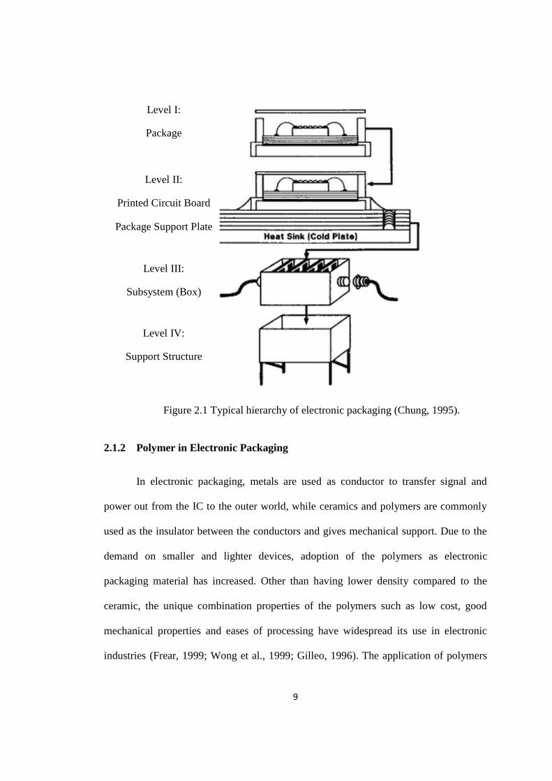
Figure 2.1 shows the typical hierarchy of electronic packaging where three
packaging levels are involved. The electronic packaging process is started with the
attachment of a single integrated circuit (IC) on the package. An IC chip is a single chip
made from semiconductor material with integration of many circuits or components.
Dependent on the application, IC can be a single component such as power transistor
for simple application, while it can have many components such as integrated

ϴ��
microprocessor in the high performance workstation. Hence, these ICs are classified by
their composition, integration level, number of transistors, function of systems,
equivalent gates and device type (Kwak & Hubing, 2007). In order to provide
interconnection, power distribution, heat dissipation and protection to the IC chip, IC
packaging, which is the first level packaging in the packaging hierarchy is involved. In
this IC packaging stage, bare IC chip is mounted directly to the substrate in the direct
chip attach (DCA) methods through the technologies such as wire bonding, flip-chip
bonding and tape-automated bonding (Stout, 1994). The substrate in this first level
packaging is normally the lead frames with specific shape which is ready for
interconnection to the next level of packaging. However, for a complete system, number
of different active and passive devices is required. Hence, second level packaging which
is also known as system-level packaging is involved. All the required components are
assembled on the system-level board and the interconnections between the components
are done through the conductor wiring. While for the interconnection between the first
level packaging and second level packaging, the connection is achieved through the
bonding of solder from the first level package to the printed wired conductive board of
the second level package (Tummala et al., 1997). For the high performance product
such as supercomputers, several processors are required. Therefore, the total system
become more complicated and several system level packages are required to provide
extremely high transactional throughput. The assembly of the system level packages is
referred as third level packaging in the hierarchy packaging. The system level packages
are assembled on the motherboard or backplane, and the connections between the
system level packages are completed with cables and connectors (Harper, 2005).
ϵ��
Figure 2.1 Typical hierarchy of electronic packaging (Chung, 1995).
2.1.2 Polymer in Electronic Packaging
In electronic packaging, metals are used as conductor to transfer signal and
power out from the IC to the outer world, while ceramics and polymers are commonly
used as the insulator between the conductors and gives mechanical support. Due to the
demand on smaller and lighter devices, adoption of the polymers as electronic
packaging material has increased. Other than having lower density compared to the
ceramic, the unique combination properties of the polymers such as low cost, good
mechanical properties and eases of processing have widespread its use in electronic
industries (Frear, 1999; Wong et al., 1999; Gilleo, 1996). The application of polymers
Level I:
Package
Level II:
Printed Circuit Board
Package Support Plate
Level III:
Subsystem (Box)
Level IV:
Support Structure

ϭϬ��
no longer constrain as an insulator. Innovation of the technologies had made polymers
an excellent semiconductors and conductors (Said, 2009). Varied application of the
polymer can be seen these days ranging from dielectric, passivation layers, encapsulants,
adhesives for die attach and underfill materials. (Rimdusit & Ishida, 2000; Shick et al.,
1998)
Polymer can be divided into two groups which are thermoplastics and
thermosets. Thermoplastics are the polymer that can repeatedly heat to soften for
remolding while thermosets are the polymer that cannot be remelted due to the cross-
linking formation during the conversion into the finished product (Rosato et al., 2000).
Table 2.1 contains the common type of thermoset and thermoplastic materials used in
electronic application, their characteristics, and applications descriptions. During the
polymerization, thermoset polymers form a three-dimensional network which is very
rigid in compared with the linear thermoplastic structure. Hence, thermoset materials
with more cross-link densities are rigid, hard, brittle and less flexible compared to the
thermoplastic materials (Gilleo, 2003).
Thermoplastics such as vinyls, polyethylene teraphthalate (polyester),
fluorocarbons, polyimides and fluorocarbon-polyimides are commonly utilized for the
application where flexibility is required, such as flexible circuit which will be discussed
later. Among all of these materials, polyimide is the most expensive raw material to be
used. However, it is still the best combination of cost and properties for high
performance application such as military. Polyester is also one of the common materials
for cost-sensitive flexible circuit but only to the low temperature application due to the
poor thermal resistance. In the polyimide was favorable as the solution to

ϭϭ��
Table 2.1.Characteristic and applications for the common type of thermoset and thermoplastic materials used in electronic industry (Harper, 2005). Materials Characteristics Applications Thermoplastics Flourocarbon Heat resistance
Superior chemical resistance
Low dielectric losses Zero water absorption Low friction
coefficient
Wire and cable insulation
Electrical components
Liquid Crystal Polymer (LCP)
High temperature and chemical resistance
High mechanical strength
Low thermal expansion
Chip carriers Sockets Connectors Relay cases
Polyester (Polybutylene terephthalate, polyethylene terephthalate, polycyclohexylene dimethylene terephthalate)
Good electrical properties
Chemical resistance High-temperature
resistance Low moisture
absorption
Connectors Sockets Chip carriers
Polyimides Superior high-temperature properties
Radiation resistance Flame resistance Good electrical
properties
Integrated-circuit applications
Insulation for electric motors
Thermosets Epoxy Resin (Bisphenol A and bisphenol F)
Excellent combination of physical, chemical, mechanical and electrical properties
Dimensional stability
Printed-wiring-board substrates
Chip carrier connectors
Bismaleimides Superior elevated-temperature performace properties
Printed-wiring-board substrates
the temperature limits of polyester due to its low coefficient of thermal expansion and
good electrical and mechanical properties (Minges & ASM International Handbook
Committee, 1989). However, the disadvantages of polyimide such as high cost, high

ϭϮ��
moisture absorption had limited its mass application in electronic industry.
Fluorocarbon is also commonly used in flexible circuit. Although it is an expensive
materials and hard to handle, but its superior dielectric properties make it suitable to be
applied in controlled impedance boards (Coombs, 1996).
In compared with thermoplastic materials, thermoset materials are generally
higher strength than that of thermoplastic (Ritchie et al., 2003). Another advantange
about the thermoset materials is they do not have a tendency to cold flow (creep) at
room temperature. This is due to the formation of tightly cross-lined three dimensional
network structure in the thermoset materials upon curing (National Research Council,
1985). These rigid thermosets are formed through the combination of two or more
components and cured by applying sufficient heat. The cured thermoset is impossible to
convert back into liquid form. The application of heat on the cured thermosets will not
melt or flow, but it will start to lose its hardness or soften where the temperature to
measure this deformation is known as glass transition temperature (Sheikh-Ahmad,
2008).

ϭϯ��
2.1.2.1 Epoxy
Epoxy resin is the most common thermoset materials used for electronic
encapsulation and printed circuit board due to their good chemical, mechanical and
electrical properties (Miao et al., 2010; Liu & Chen, 2004). Although epoxy resin
covers a range of materials with widely differing characteristics and costs, but a
multifunctional materials/blends of epoxy resins can be developed to fill the niche
between lower-cost regular epoxies and high-performance resins, and give an extended
operational temperature range at lower cost than polyimide (Coombs, 2001). The
properties of the epoxy film such as thermal stability, electrical conductivity and
thermal conductivity can be easily altered through the selection of fillers (Alapati &
Thomas, 2008; Cheng et al., 2008; Liu et al., 2004; Teh et al., 2008). Apart from that,
the simpler fabrication process of epoxy based thin film composite allows high volume
production.
There are many types of epoxy resins in the market and Figure 2.2 shows the
categories of these epoxy resins. The epoxy resins are categorized into two main
categories which are glycidyl epoxy resins and non-glycidyl epoxy resins (Dunn, 2003).
For glycidyl epoxy resins such as diglycidyl ether of bisphenol A (DGEBA), diglycidyl
ether of bisphenol F (DGEBF) and epoxy novolac, they are prepared via condensation
reaction of appropriate dihydroxy compound, dibasic acid or a diamine and
epichlorohydrin. For non-glycidyl epoxy resins such as aliphatic and cycloaliphatic
epoxy resins, they are formed by peroxidation of olefinic double bond (Dunn, 2003).
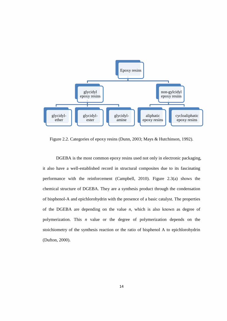
ϭϰ�
Figure 2.2. Categories of epoxy resins (Dunn, 2003; Mays & Hutchinson, 1992).
DGEBA is the most common epoxy resins used not only in electronic packaging,
it also have a well-established record in structural composites due to its fascinating
performance with the reinforcement (Campbell, 2010). Figure 2.3(a) shows the
chemical structure of DGEBA. They are a synthesis product through the condensation
of bisphenol-A and epichlorohydrin with the presence of a basic catalyst. The properties
of the DGEBA are depending on the value n, which is also known as degree of
polymerization. This n value or the degree of polymerization depends on the
stoichiometry of the synthesis reaction or the ratio of bisphenol A to epichlorohydrin
(Dufton, 2000).
Epoxy resins
glycidyl epoxy resins
glycidyl-ether
glycidyl-ester
glycidyl-amine
non-gylcidyl epoxy resins
aliphatic epoxy resins
cycloaliphatic epoxy resins

ϭϱ��
(a)
(b)
Figure 2.3. Chemical structure for (a) DGEBA and (b) DGEBF (Mays & Hutchinson, 1992; Balachandran, 2000)
DGEBF is the simplest novolac that prepared by the condensation of
formaldehyde with phenolic substance under acidic conditions, and followed by
epoxidation (Rabilloud, 1997). This type of epoxy resin has much attractive application
that is paralleling with the DGEBA (Ardebili & Pecht, 2009). In compared with
DGEBA, DGEBF posses lower viscosity and lower tendencies to crystallize. Figure
2.3(b) shows the chemical structure of DGEBF. It is noticed that the chemical structure
of DGEBF has the same general structure as DGEBA. Therefore, the physical and
chemical properties of these two epoxy resin are almost similar. The small difference in
the chemical structure is actually contributed to the lower viscosity on DGEBF in
compared with the DGEBA (Balachandran, 2000).
2.1.2.2 Curing Agents
The widespread usage of epoxy resins from large industry such as structural
industry to small discrete industry such as electronic industry is due to their unique

ϭϲ��
combination of properties when it cured (Tagami et al., 2008; Aziz, 2010; Kim et al.,
2001). The characteristic of the cured epoxy resins are dependent on the curing system
used for the formation of crosslinking in the epoxy resin. For the crosslinking reaction
to occurs, two types of reaction are involved which are addition reaction and catalytic
reaction (Craver & Carraher, 2000). For the addition reaction, the curing agent molecule
which is also known as hardener molecule will chemically bonded to the epoxide group
and serve as a bridge of crosslinking in the epoxy resins. Meanwhile for the catalytic
reaction, the curing agent will serve as catalyst, encouraging the self-polymerization of
the resin (Goosey, 1999).
There are hundreds of curing agents available in the market these days. These
curing agents can be divided into four major categories which are amines, anhydrides,
imidazoles and catalytic agents (as shown in Figure 2.4) (Lubin & Peters, 1998).
Amines are the substitution of hydrogen molecule(s) of ammonia (NH3) in the
hydrocarbon and the structure of this organic compound is R NH2. They can be
aliphatic (straight chain or branched), alicyclic (closed ring) or aromatic (closed ring
and exhibit a number of substantial peculiarities of their own) depending on the types of
hydrocarbon involved (Gooch, 2010). Figure 2.5 shows the curing reaction of the epoxy
resin and amines. In the case of aliphatic amine, the R is an alkyl group while for
aromatic amine, the R is aryl group. Alicyclic amine is similar to those simple alkyl
amines, but it exhibit hazardous properties. Aliphatic is commonly used for room
temperature curing due to its rapid reaction with epoxy resin. In the other words,
aliphatic amine has the shortest pot life. While for aromatic amine, the steric hindrance
of the aromatic ring allows slow curing in the room temperature. Heat is normally

ϭϳ��
involved to accelerate the curing. As compared with aliphatic amine, aromatic amine
gives an excellent heat resistance and chemical resistance due to its aromatic structure
(Licari & Swanson, 2011).
Figure 2.4. Categories of curing agents
Anhydride curing agents which derived from a diacid by dehydration are also
used extensively for the curing of epoxy resins (www.scribd.com). Figure 2.6 shows the
curing mechanism of epoxy by anhydride curing agents. In contrast with amine,
anhydrides are less reactive, therefore the curing of the epoxy by anhydrides is slow,
and temperature of curing at around 150 170oC is required for at least 2 hours
Curing agents
Amines
Aliphatic amines
Cycloaliphatic amines
Aromatic amines
Anhydrides
Aliphatic anhydrides
Aromatic anhydrides
Alicyclic anhydrides
Catalytic agents
Lewis acids
Lewis bases
Imidazoles

ϭϴ��
(Campbell, 2004). However, the curing rates can be accelerated with the addition of
catalytic curing agents such as tertiary amine (Jin et al., 2006).
R NH3 + H2CHC
O
RHN
H2C
HC
OH
Formation of secondary amine and more hydroxyl groups
RHN
H2C
HC
OH
+ H2CHC
O
R NH2C
HC
OH
H2C CH
OH
�
�
�Formation of tertiary amine
R NH2C
HC
OH
H2C CH
OH
+ H2CHC
OR N
H2C
HC
OH
H2C
H2C CH
OHH2C
2O
HC
O
CH
Cross-linking through reaction of hydroxyl groups
Figure 2.5. Curing mechanism of epoxy by amine curing agents (Licari & Swanson, 2011)
Amine curing
Epoxide group from epoxy
Epoxide group from epoxy
Epoxides group from epoxy

ϭϵ��
O
O
O
R OH +O
OR
O
O
H
Opening of anhydride ring by hydroxyl group from epoxy to form carboxylic acid
group
O
OR
O
O
H+ H2C
HC
OO
OR
O
O
H2C
HC
OH �
Etherification of hydroxyl group by epoxide group from epoxy
O
OR
O
O
H2C
HC
OH
+ H2CHC
O
O
OR
O
O
H2C
HC
OH2C
HC
OH
Reaction of hydroxyl group with epoxide group from epoxy
Figure 2.6. Curing mechanism of epoxy by anhydride curing agents (Licari & Swanson, 2011)
There are three types of anhydrides which are aromatic anhydrides, alicyclic
anhydrides and aliphatic anhydrides. The solid form of aromatic anhydrides is
commonly used in powder paints for powder molding, while the solutions in liquid
Hydroxyl group from epoxy Anhydride Formation of carboxylic
acid group
carboxylic acid group
Epoxide group from epoxy
Epoxide group from epoxy

ϮϬ��
anhydrides are used in insulating coating (Three Bond Technical News, 1990). For the
application with epoxy resins, alicyclic anhydrides shown in Figure 2.7 are normally
used. Polycarboxylic anhydrides are one of the example of aliphatic anhydrides. It is
formed through the dehydration condensation reaction between aliphatic dibasic-acid
molecules. The cured product by these anhydrides gives excellent flexibility and
thermal shock resistance (Kulshreshtha & Vasile, 2002; Goosey, 1999).
O
O
O
O
O
O
O
O
O�
�
�
O
O
O
O
O
O
O
O
O
HO
OCl
Cl
CCl2 O
O
O
Figure 2.7. Types of alicyclic anhydrides commonly used with epoxy resin (Lubin & Peters, 1998).
Catalytic curing agents are actually Lewis bases and Lewis acids (Craver &
Carraher, 2000). Compounds that contain a free pair of electrons are Lewis bases, such
as tertiary amines. While for Lewis acids, they are compounds that accept a pair of
electrons, for example, boron trifluoride. Lewis acids is very reactive, highly volatile
and toxic, this gives very short pot life. However, the complexes of Lewis acids and
Phthalic anhydride Tetrahydrophthalic anhydride
Hexahydrophthalic anhydride
Pyromellitic dianhydride
Trimellitic anhydride
Chlorendic anhydride

Ϯϭ��
bases are very stable, until it been heated to certain temperature for the dissociation of
complexes into reactive species for curing mechanism (Licari, 2003; Lubin & Peters,
1998). However, the polymerization reactions by the dissociation of these complexes
are actually similar to those curing of epoxy resin by tertiary amine, as shown in Figure
2.8.
R3N + H2CHC
O
R3NH2C
HC
O �
�
(a) Ring opening
R3NH2C
HC
O
+ H2CHC
O
R3NH2C
HC
O
H2CHC
O �
(b) Cross-linking
Figure 2.8. Polymerization reaction of epoxy by Lewis bases (a) ring opening, (b) cross-linking (Licari & Swanson, 2011).
Imidazoles, the strong organic bases and good nucleophiles are the most
common curing accelerator or co-curing agents that used in epoxy adhesives for
electronic application. Today, imidazoles have become an optional curing agent for
time constraint application (Hamerton, 1996). The curing mechanism of epoxy by
imidazoles is shown in Figure 2.9. In the beginning of homopolymerization of epoxy
resins by imidazoles, zwitterion is formed which rearranges to 1:1 adduct by internal
proton transfer. This etherification reaction occurs through the first nucleophilic attack
Lewis bases
Epoxide group from epoxy

ϮϮ��
H2CHC
O
CH2HC
O
HN N:
R4
R2
+ + N N
R4
R2
H2C
HC
O
H2C
HC
OH
�
Nucleophilic attack by the unsubstituted nitrogen atom of the imidazole ring
N N
R4
R2
H2C
HC
O
H2C
HC
OH
+ +CH2HC
O
H2CHC
O
N N
R4
R2
H2C
HC
O
H2C
HC
OH2C
HC
O
H2C
HC
OH �
Anionic polymerization of epoxy
Figure 2.9. Curing mechanism of epoxy by imidazoles (Omrani et al., 2008).
by the unsubstituted nitrogen atom in imidazole ring. The newly formed unsubstituted
nitrogen is then going through nucleophilic reaction, and a second epoxy group is
opened to give the 2:1 adduct. These adducts generations are the slow initial rate of
epoxy conversion. Polyetherification reaction are then initiated by the 2:1 adduct which
Epoxide group from epoxy
Epoxide group from epoxy
Imidazoles O-/OH - Adduct
Epoxide group from epoxy
Epoxide group from epoxy
O-/OH - Adduct

Ϯϯ��
are able to promote the anionic polymerization of the epoxy (Cognard, 2005). In the
other words, the polymerization process are believed to be catalyst by the 2:1 adduct
which contains the nucleophilic alkoxide ion (Heise & Martin, 1989; Rabilloud, 1997).
2.2 Polymer Composite in Electronic Packaging
2.2.1 Introduction
The demand trend on the small size and high performance electronics has driven
changes in the electronic packaging requirements. This has raised issue such as
reliability, weight-critical system, warpage of the IC chips and package, cost, and poor
heat management which are the major failure factor of the electronic devices (Huang et
al., 2006). Therefore, the innovation of the technologies had expanded the application of
polymer other than used for insulation purpose, and brought further into the electronic
packaging throughout the three packaging level (Lupinski & Moore, 1989; Thompson et
al., 2004). However, properties of the polymer itself are still far to meet the packaging
design requirements. Hence, polymer composite materials which have tailorable
properties are created especially for this electronic packaging.
Glass fiber reinforced polymer (GFRP), the well established packaging materials
has replaced the bakelite and masonites in printed circuit board. Application of GFRP
has solved the weight and reliability issues in the electronic packaging
(http://www.4pcb.com/pcb/Ϳ. Nevertheless, this polymer composite is only utilized in
the second and third level of packaging hierarchy. In order to continue solving the
packaging issue arises in line with the miniaturization especially in the first level of
packaging hierarchy, new composite materials which distinguish them from the GFRP
Ϯϰ��
is developed. This packaging material is known as advanced composites (Chung, 1995).
The choice of the fillers, size and shape of the fillers are taking into the account when
te for first level of packaging
hierarchy. Many research works have been done with the incorporation of suitable
ceramic and metal fillers in this advanced composite to make the properties such as
dielectric, electrical conductivity, thermal conductivity, coefficient of thermal
expansion (CTE) and some mechanical properties tailorable to the required value (Bae
et al., 2004; Ho et al., 2008; Hodgin & Estes, 1999). Moulding compound, thermal
interface materials and underfills are the most common application of these advanced
composites (Kim & Bae, 2004, Yu et al., 2007; Lee & Yu, 2005).
2.2.2 Factors Influence Polymer Composite
Polymer composites are the multifunctional materials which their properties can
be tailored to meet the requirement of the electronic packaging. It is generally known
that polymer matrices are weak, low stiffness and viscoelastic materials. They have very
poor mechanical properties, low thermal and electrical conductivity (Harper, 2002). The
properties of the polymer composites are contributed by the fillers or reinforcements
that incorporated into it. Their properties are strongly dependent on the types of fillers
or reinforcements, volume fraction or loading, dispersion as well as the microstructural
of these fillers or reinforcements (Tong, 2010).
2.2.2.1 Types of Fillers
Depending on the required properties, types of fillers are normally the first thing
to concern when it comes to the materials selection for the fabrication of polymer