Embed Size (px)
Citation preview

1
Fabrication and Assembly of Ultrathin Silicon Solar Microcells Integrating
Electrical Passivation and Anti-reflection Coatings
Yuan Yao, Eric Brueckner, Lanfang Li, and Ralph Nuzzo
Supplementary Information
Figure S1 shows a schematic overview of the fabrication process.
Cleaning
The process started with a boron-doped Czochralski silicon wafer (“prime” grade,
3-inch diameter, (111) ±0.1° orientation, 7.5-10 Ω·cm, 380 µm thickness, Silicon
Materials).Wafers were rinsed with acetone and isopropyl alcohol (IPA). Prior to all high
temperature processes, RCA cleaning procedures were used, detailed below:
RCA1 Clean
Etch in RCA1 solution (H2O:NH3·H2O:H2O2= 5:1:1) at 80°C for 10 min
RCA2 Clean
Etch in RCA1 solution (H2O:HCl:H2O2= 5:1:1) at 80°C for 10 min
Native oxide on the wafer was removed by buffered oxide etchant (BOE 6:1, Transene)
before and after each cleaning step.
Phosphorus Doping
The cleaned wafers were first doped by solid-state sources of phosphorus (PH-
1000N, Saint Gobain). Etching the phosphosilicate glass (PSG) layer in BOE 10:1 and
RCA cleaning completed the doping process.
Phosphorous doping over a variety of temperatures (900°C, 950°C, and 1000°C)
and times (5 min, 15 min, and 30 min) was conducted to ultimately optimize conversion
Electronic Supplementary Material (ESI) for Energy & Environmental ScienceThis journal is © The Royal Society of Chemistry 2013

2
efficiency of the µ-cells. To directly compare the effect of doping time and temperature
parameters, three batches of three wafers were processed simultaneously, each wafer
within the batch doped for a different time (Batch 1: 1000°C, Batch 2: 950°C, Batch 3:
900°C). To eliminate possible variations in light absorption from the anti-reflective,
oxide layers (the thickness of oxide on device differs from batch to batch), the µ-cells
were immersed in BOE 6:1 to remove all oxide prior to testing. Figure S2 shows
normalized efficiency vs. doping time for the three temperatures of interest. The doping
conditions giving the highest conversion efficiency in each batch were 1000°C for 5 min,
950°C for 5 min, and 900°C for 15 min, giving sheet resistance values of 22 Ω/, 80 Ω/,
and 78 Ω/, respectively, measured by four point probe (Pro4, Signatone). These
conditions were then directly compared in a fourth batch to eliminate batch-to-batch
variability. Figure S3A shows the doping profiles measured by quantitative secondary-
ion mass spectrometry (SIMS) and Figure S3B shows averaged I-V curves of cells doped
at 900°C, 950°C, and 1000°C for 15 min, 5 min, and 5 min, respectively. Table 1 and
Figure S4 shows the parameters of Jsc, Voc, η, and FF. The data shows that doping at
900°C for 15 min gives the highest conversion efficiency, leading us to adopt this as the
standard protocol for µ-cell fabrication.
Temp (°C) Jsc (mA/cm2) Voc (V) η (%) FF
900 (15 min) 27.15 0.538 10.6 0.727
950 (5 min) 26.55 0.541 10.0 0.699
1000 (5 min) 23.83 0.543 9.3 0.719
Table 1
Electronic Supplementary Material (ESI) for Energy & Environmental ScienceThis journal is © The Royal Society of Chemistry 2013
3
Thermal Oxidation and Photolithography
A top oxide mask layer was then grown by wet oxidation at 1000 °C for 80-100
min under steam atmosphere (<0.2 LPM O2 flow through boiling DI water) in a quartz
tube furnace following RCA1 and RCA2 cleanings outlined above. The lateral
dimensions of the µ-cells were defined by standard photolithographic processing
(AZ5214-E, AZ Electronic Materials):
Spin-coat hexamethyldisilazane (HMDS) at 5000 rpm for 30 sec
Spin-coat AZ5214-E at 5000 rpm for 30 sec
Softbake at 110°C for 60 sec
Expose 310 mJ/cm2 at 320 nm (Karl Suss MJB3 mask aligner)
Develop in metal ion free (MIF) 327 for ~100 sec
O2 descum (20 sccm, 250 mTorr, 50 W) for 60 sec
Hardbake at 110°C for 180 sec
The oxide not covered by the photoresist was then removed by BOE 6:1 (~12 min).
Inductively coupled plasma reactive ion etching (ICP-RIE, Surface Technology Systems)
was utilized to define the vertical depth of the trench structures. Standard Bosch
Processing conditions were used: chamber pressure of 81.5 mTorr, etching for 7 sec/cycle
with 130 sccm SF6 and 13 sccm O2 under 600 W coil power and 12 W platen power, then
passivating for 5 sec/cycle with 110 sccm C4F8 under 600 W coil power and 0 W platen
power. Etch times were controlled such that an etch depth of 35-40 µm was achieved,
typically 75 cycles. The remaining photoresist was then removed by sonicating in
acetone and RCA1 cleaning.
Brief Undercut and Sidewall Oxidation
Electronic Supplementary Material (ESI) for Energy & Environmental ScienceThis journal is © The Royal Society of Chemistry 2013
4
A short anisotropic etching step of the wafer was performed in 25 wt.%
tetramethylammonium hydroxide solution (TMAH, Sigma-Aldrich) at 70°C for 2 min to
achieve a canopy-type structure. The exposed sidewalls (110) of cells etched at ~1
µm/min according to cross-sectional SEM images shown in Figure 1B. After RCA
cleanings, a second wet oxidation step (1000 °C, 20-25 min) formed an oxide layer on the
side and bottom of the trenches and increased the oxide thickness on top of the cells as
well, shown in Figure S5A.
Flood RIE and Undercut
The oxide on the bottom of the trenches was selectively removed by reactive-ion
etching (Plasma Therm 790 series) using CHF3 (20 sccm) and O2 (8 sccm) under 50
mtorr and 175 W for ~9 min. This dry etch is pseudo-anisotropic such that little oxide on
the sidewall was consumed (Figure S5B). After immersion in BOE 6:1 for ~20 sec, the
wafer was immersed into 25% TMAH solution at 80°C for ~90 min to fully undercut the
µ-cells and release them from the substrate except at anchor locations.
Boron Doping
After RCA cleaning, the back surface field was formed by solid-source boron
doping (BN-975, Saint Gobain) at 1000 °C for 30 min. The borosilicate glass (BSG)
layer was etched in 20:1 HF for ~2 min. Oxide remaining on the top and sidewall
surfaces (Figure S5C) now serves as passivation and anti-reflection layers.
Patterning Top Contacts
Square contacts (50 µm ×50 µm) were defined through photolithography with a
photoresist (AZ P4620, Clariant):
Spin-coat HMDS at 2000 rpm for 30 sec
Electronic Supplementary Material (ESI) for Energy & Environmental ScienceThis journal is © The Royal Society of Chemistry 2013

5
Spin-coat AZ5214-E at 1000 rpm 10 sec, then at 2000 rpm for 30 sec
Softbake at 65°C for 5 min and then at 95°C for 20 min,
Expose 410 mJ/cm2 at 365 nm
Develop in 3:1 AZ400K(AZ Electronic Materials) for ~1 min
Expose under UV-generated ozone for 2 min
Hardbake at 65°C for 30 min (ramp from 35°C with a ramp rate of 0.5°C/min)
The oxide not protected by the photoresist was then removed by BOE 6:1 (~5.5 min) and
Ti (10 nm) /Au (300 nm) contact pads were formed by e-beam evaporation and
photoresist lift-off in acetone.
Statistical Analysis of Fabricated Si Solar µ-Cells
To test the large-area reliability of the fabrication process, we transferred µ-cells
from the entire patterned wafer area. Specifically, every sixth device in all six rows was
picked-up with a PDMS stamp and transferred to a glass substrate (discussed
subsequently) for I-V testing. The µ-cells were tested under simulated AM1.5D
illumination of 1000 W·m-2 at room temperature prior to planarization of the µ-cells on an
anodized Al plate to minimize reflection from the back plane. Using the top surface area
of the µ-cells as the device area, the PV metrics of Jsc, Voc, η, and FF were measured and
plotted with histograms shown as insets (Figure S6 and Figure 2C).
Transfer Printing µ-Cells
The receiving substrate was made by spin-coating a UV-curable polymer (NOA61,
Norland Products, 3000 rpm for 45 sec) on a pre-cleaned glass slide (5 cm × 5 cm × 2
mm ) and partially curing under UV light (1260 mJ/cm2 at 365 nm) with a Karl Suss
Electronic Supplementary Material (ESI) for Energy & Environmental ScienceThis journal is © The Royal Society of Chemistry 2013

6
MJB3 mask aligner. Bottom electrodes were then deposited by e-beam evaporation of Ti
(10 nm) /Au (300 nm) through a shadow mask.
Microcells were selectively picked up by a PDMS (10:1 ratio of pre-polymer to
initiator, Sylgard 184, Dow Corning) stamp with pyramidal structures and printed on the
receiving substrate with an automated transfer printing machine. By applying modest
pressure on the inked stamp to the receiving substrate, excellent electrical contact was
achieved between the bottom electrode and device. Step and repeat printing allowed
formation of arrays with arbitrary configurations. The fabrication of the pyramid PDMS
stamp and the manipulation of the automated machine were described elsewhere (see Ref.
36).
After printing, the µ-cells were tested and baked at 150 °C on hotplate for 10 min.
This postbake step possibly caused the partially cured NOA layer to reflow and
intimately coat the bottom side of the µ-cell, preventing liquid pre-polymer to flow
underneath the device and block the back contact in the following planarization step.
Planarization
A flat PDMS block (10:1 ratio of pre-polymer to initiator) was laminated on top
of the printed devices to achieve conformal contact with the µ-cells. Silica particles (30
µm diameter, SPI) were dispersed on the substrate around the device area to support the
PDMS stamp and avoid sagging. Another UV-curable polymer (NOA73, Norland
Products) was dispensed in a reservoir created in the PDMS block with a 3 mm biopsy
punch. The liquid pre-polymer flowed by capillary action to fill the air gap between the
PDMS and substrate. The entire system was then exposed under UV light to cure the
NOA, before PDMS was peeled off from the substrate, leaving the µ-cells embedded in
Electronic Supplementary Material (ESI) for Energy & Environmental ScienceThis journal is © The Royal Society of Chemistry 2013
7
the NOA matrix. A profilometry line scan (Figure S8A) of the resulting planarization
layer shows minimal topological variation between cells (~5 µm).
Interconnection
Interconnecting the planarized µ-cells was accomplished by manually aligning a
stencil mask (two pieces of Scotch® tape) to form the shape of the interconnect. A small
volume (~0.5 mL) of Ag paste (Ted Pella, PELCO® Conductive Silver 187) was
dispensed on one end, using a razor blade to “squeegee” the Ag paste over and into the
stencil mask. The Scotch® tape stencil mask was peeled away immediately, leaving
behind a well-formed interconnection line ~150 µm wide and ~50 µm tall (Figure S8B).
The Ag paste line was cured in air at room temperature for 30 min prior to any electrical
measurements.
Measurements under Concentration
To aid thermal and electrical conduction due to intense illumination and increased
photocurrent generation, respectively, from concentrated solar flux, devices were
assembled differently than the procedure described above. After device fabrication, the
µ-cells were conformally contacted by a PDMS stamp and lifted off from the donor wafer.
Thin-film metal ohmic contacts (~150 µm wide, Ti (5 nm)/Au (200 nm)) were e-beam
evaporated on the backside of the µ-cells through a shadow mask. The µ-cells were then
embedded in a thin (~200 µm) line of uncured Ag epoxy (E4110, Epoxy Technology) on
a glass slide. The glass slide/Ag epoxy/µ-cell/PDMS system was baked on a 150ºC hot
plate for 15 min. Following the baking step, the PDMS stamp was slowly removed,
leaving the µ-cells printed on a cured Ag epoxy matrix serving as the interconnection on
the backside of the devices. There was not a subsequent planarization step with NOA.
Electronic Supplementary Material (ESI) for Energy & Environmental ScienceThis journal is © The Royal Society of Chemistry 2013

8
During solar measurements under concentration, the glass slide was mounted on an
anodized aluminum plate with a 3 inch fan used to cool the µ-cells. Concentration ratios
(x) for Figures 5E and 5F were calculated by the following expression:
, ,
where Isc,conc and Isc,1sun is the short-circuit current for a µ-cell under concentration and 1
sun, respectively.
Solar µ-Cell Characterization
I-V characteristics of the µ-cells were measured with a source meter (Keithley,
Model 2400) under a full-spectrum solar simulator (Model 91192, Oriel) with AM 1.5D
filter calibrated to 1000 W·cm-2 at room temperature using a Si reference cell (Model
91150V, Newport-Oriel). Measurements under solar concentration were obtained by
placing a convex lens (Model LH-2 M4 KBX145 F62.9, Newport) in the beam path.
Different concentration ratios were obtained by translating the lens vertically.
Due to the inherent transparency of printed arrays of these µ-cells, reflection from
the subjacent layers will have a significant impact on PV measurements. We suppressed
reflection from the solar simulator’s sample stage by mounting the glass substrate on an
anodized Al (AA) plate to obtain PV metrics with minimal influence of reflected light.
Figure S9 shows reflectivity data, relative to a Spectralon® target, of the anodized Al
(AA) plate used for PV measurements. To elucidate enhancements to the PV metrics of
printed µ-cells from diffuse reflection, the glass substrate was also mounted on a
Spectralon® target, as shown in Figure 5A, in some measurements. We distinguish
reported PV metrics when using this diffuse backside reflector by using subscript “BSR”.
Electronic Supplementary Material (ESI) for Energy & Environmental ScienceThis journal is © The Royal Society of Chemistry 2013

9
For devices without oxide, I-V characteristics were measured right after a 5.5 min
etch in BOE 6:1 as well as a few days later after the formation of the native oxide layer
on an AA plate without planarization. (See Figure S7A and Table2). The devices show a
further degradation after the surface Si-H bonds formed during BOE etch were oxidized
in air. The data with the native oxide layer is used in Figure 3A.
Jsc (mA/cm2) Voc (V) Efficiency (%) FF
With Oxide 28.08 0.515 10.89 0.753
After BOE 19.85 0.501 7.54 0.758
Without Oxide (With Native Oxide)
19.08 0.481 6.80 0.740
Table 2
EQE measurements were taken using an OL750 spectroradiometer with devices
embedded in NOA layer with top contact lines. The top interconnects for devices in
Figure 3B and Figure S7E were formed by either sputtering a Ti (10nm)/Al (300nm)
metal line or directly painting a silver paste/epoxy line through a stencil mask onto the
cell. All EQE results were normalized to percentage based on device performance under
AM1.5D solar spectrum measured on a non-reflective AA plate without planarization to
eliminate waveguiding effects.
Methods for calculating the AR effects from the top oxide
The reflections on the top surface of the device were calculated based on
refractive indices of thermal oxide (n2) and silicon (n1) at different wavelengths (λ),
assuming a normal incidence of the incoming solar radiation. (Refractive indices at
different wavelength for single-crystalline silicon and fused silica were taken from
Electronic Supplementary Material (ESI) for Energy & Environmental ScienceThis journal is © The Royal Society of Chemistry 2013
10
“Handbook of Optical Constants of Solids, Edward D. Palik. Academic Press, Boston,
1985” and “Handbook of Optics, 3rd edition, Vol. 4. McGraw-Hill 2009”, respectively.)
For devices without oxide, the top surface reflection (R1) under air was calculated
as
For devices with oxide with a certain thickness (t), the top surface reflection (R2)
was calculated as
where
The relative optical enhancement (E) by adding a thermal oxide AR layer was
then defined as
The EQE for a device with AR coating but without passivation was then
estimated as
The difference between these two EQE curves were then integrated with the AM
1.5D solar spectrum to get the simulated current density enhancement from an AR layer
on a device without passivation.
Electronic Supplementary Material (ESI) for Energy & Environmental ScienceThis journal is © The Royal Society of Chemistry 2013

11
For the blue dashed curve in Figure 3B, 250 nm was used as the oxide thickness
for calculation, as determined by a cross-sectional SEM image (Figure S7B) for another
device on the same donor wafer.
Electronic Supplementary Material (ESI) for Energy & Environmental ScienceThis journal is © The Royal Society of Chemistry 2013

12
SI Figure Captions
Figure S1 Schematic illustration of the fabrication protocol for creating Si solar µ-cells.
Figure S2 Efficiency normalized to the maximum efficiency for each data series (i.e.,
doping temperature) vs. phosphorous doping time. The data shows that the maximum
efficiency is achieved at doping times of 15 min, 5 min, and 5 min at doping temperatures
of 900°C, 950°C, and 1000°C, respectively.
Figure S3 (A) SIMS depth profile of phosphorous concentration in samples doped at
different conditions; (B) J-V curves of µ-cells doped at different conditions measured on
an AA plate without planarization. (900°C, 15 min: black, 950°C, 5 min: red; 1000 °C,
5min: blue)
Figure S4 Performance metrics of devices doped at different conditions measured on an
AA plate without planarization: (A) Jsc; (B) Voc; (C) Efficiency; and (D) Fill factor.
Figure S5 Cross-sectional SEM images of Si µ-cells (blue) with thermally grown oxide
layers (pink) on the top (left frame) and sidewall (right frame) surface after different
fabrication steps: (A) Sidewall oxidation; (B) Flood RIE; and (C) Full device fabrication.
Figure S6 Statistical analyses and histogram plots (insets) of device performance metrics
measured on an AA plate without planarization: (A) Jsc; (B) Voc; and (C) Fill factor.
Electronic Supplementary Material (ESI) for Energy & Environmental ScienceThis journal is © The Royal Society of Chemistry 2013

13
Figure S7 (A) J-V characteristics of devices with oxide (black), right after BOE etch
(green) and after formation of a native oxide layer (red); (B) Cross-sectional SEM images
of a Si µ-cell for EQE measurement with top oxide thickness of ~250 nm; (C) Calculated
top surface reflections for devices without oxide (red) and with 250 nm thermal oxide
(black); (D) Simulated relative AR enhancements for a µ-cell with 250 nm top oxide; (E)
External quantum efficiencies (EQE) of passivated µ-cells with various oxide thickness.
Figure S8 (A) Profilometry line scan across three printed Si solar µ-cells following
planarization; (B) Profilometry line scan across a Ag paste interconnect.
Figure S9 Reflectance of the non-reflective anodized aluminum (AA) plate.
Electronic Supplementary Material (ESI) for Energy & Environmental ScienceThis journal is © The Royal Society of Chemistry 2013
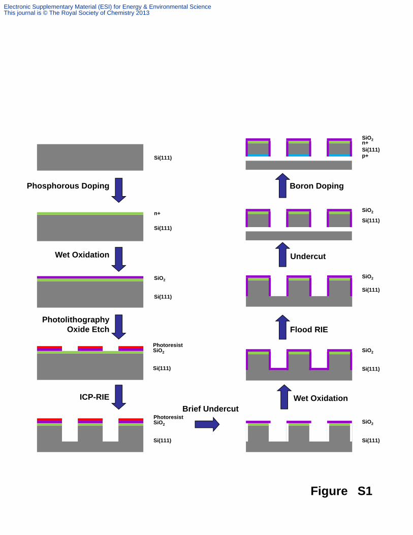
Figure S1
Wet Oxidation
PhotolithographyOxide Etch
ICP-RIEBrief Undercut
Flood RIE
Undercut
Phosphorous Doping Boron Doping
Si(111)
Wet Oxidation
Si(111)
n+
PhotoresistSiO2
Si(111)
SiO2
Si(111)
PhotoresistSiO2
Si(111)
SiO2
Si(111)
SiO2
Si(111)
SiO2
Si(111)
SiO2
Si(111)
SiO2
p+
n+Si(111)
Electronic Supplementary Material (ESI) for Energy & Environmental ScienceThis journal is © The Royal Society of Chemistry 2013
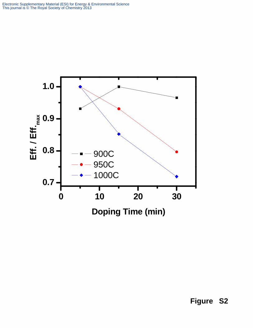
Figure S2
0 10 20 30
0.7
0.8
0.9
1.0
max
Doping Time (min)
900C 950C 1000C
Electronic Supplementary Material (ESI) for Energy & Environmental ScienceThis journal is © The Royal Society of Chemistry 2013

Figure S3
0.0 0.1 0.2 0.3 0.4 0.5 0.60
5
10
15
20
25
30
35
900°C 950°C 1000°CJ ba
se (
mA
/cm
2 )
V (V)
0 500 1000 1500 20001E15
1E16
1E17
1E18
1E19
1E20
1E21
Pho
s. C
onc.
(c
m-3
)
Depth (nm)
900°C 950°C 1000°C
A
B
Electronic Supplementary Material (ESI) for Energy & Environmental ScienceThis journal is © The Royal Society of Chemistry 2013

Figure S4
900 950 100023
24
25
26
27
28
J sc (
mA
/cm
2 )
Doping Temperature (°C)
900 950 10000.52
0.53
0.54
0.55
0.56
Voc
(V
)
Doping Temperature (°C)
900 950 1000
0.66
0.68
0.70
0.72
0.74
0.76
0.78
Fill
Fac
tor
Doping Temperature (°C)
900 950 1000
9.0
9.5
10.0
10.5
11.0
Effi
cien
cy (
%)
Doping Temperature (°C)
A B
C D
Electronic Supplementary Material (ESI) for Energy & Environmental ScienceThis journal is © The Royal Society of Chemistry 2013
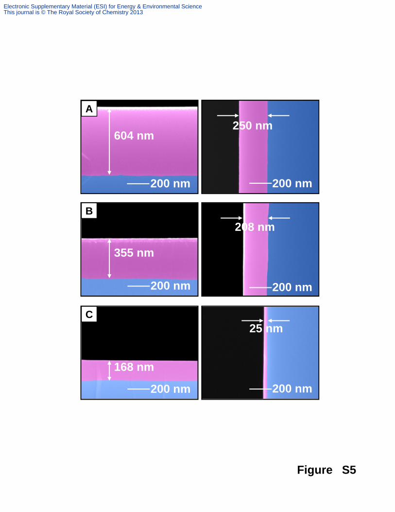
Figure S5
200 nm
200 nm
200 nm
604 nm
355 nm
168 nm
200 nm
200 nm
200 nm
250 nm
208 nm
25 nm
A
B
C
Electronic Supplementary Material (ESI) for Energy & Environmental ScienceThis journal is © The Royal Society of Chemistry 2013

Figure S6
0 10 20 30 40 50 60 700.40
0.42
0.44
0.46
0.48
0.50
0.52
0.54
Voc
(V
)
Device #
Mean = 0.5114StdDev = 0.00432
0 10 20 30 40 50 60 705
10
15
20
25
30
J sc (
mA
/cm
2 )
Device #
Mean = 26.27StdDev = 0.375
24 25 26 27 28 290
5
10
15
Cou
nt
Jsc(mA/cm 2)
0.48 0.50 0.52 0.54 0.560
5
10
15
Cou
nt
Voc (V)
0 10 20 30 40 50 60 700.00.10.20.30.40.50.60.70.80.9
Fill
Fac
tor
Device #
Mean = 0.745StdDev = 0.0114
68 72 76 800
5
10
15
Cou
nt
Fill Factor (%)
A
B
C
Electronic Supplementary Material (ESI) for Energy & Environmental ScienceThis journal is © The Royal Society of Chemistry 2013

Figure S7
A
0.0 0.1 0.2 0.3 0.4 0.5 0.60
5
10
15
20
25
30
35
With oxide After BOE Without oxideJ ba
se (
mA
/cm
2 )
V (V)
C
B
D
250 nm
200 400 600 800 1000 12000.8
0.9
1.0
1.1
1.2
1.3
1.4
1.5
1.6R
elat
ive
AR
Enh
ance
men
ts
Wavelength (nm)
250 nm oxide
200 400 600 800 1000 12000
10
20
30
40
50
60
70
Ref
lect
ion
(%)
Wavelength (nm)
with oxide without oxide
E
200 400 600 800 1000 1200
0
20
40
60
80
100
EQ
E (
%)
Wavelength (nm)
Dev1 Dev2
Electronic Supplementary Material (ESI) for Energy & Environmental ScienceThis journal is © The Royal Society of Chemistry 2013
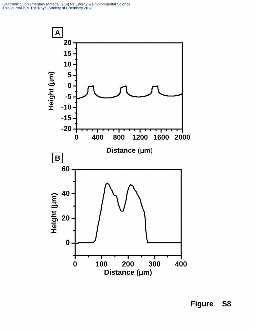
Figure S8
0 400 800 1200 1600 2000-20
-15
-10
-5
0
5
10
15
20
Hei
ght
( µµ µµm
)
Distance (µµµµm)
0 100 200 300 400
0
20
40
60
Hei
ght (
µµ µµm)
Distance ( µµµµm)
A
B
Electronic Supplementary Material (ESI) for Energy & Environmental ScienceThis journal is © The Royal Society of Chemistry 2013

Figure S9
400 600 800 1000 1200 1400
0
20
40
60
80
100
Wavelength (nm)
Electronic Supplementary Material (ESI) for Energy & Environmental ScienceThis journal is © The Royal Society of Chemistry 2013