Embed Size (px)
Citation preview
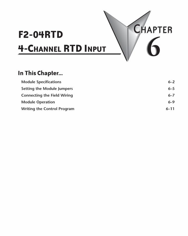
F2-04RTD 4-Channel RTD InpuT 1466
ChapterChapterChapter
In This Chapter...Module Specifications 6–2
Setting the Module Jumpers 6–5
Connecting the Field Wiring 6–7
Module Operation 6–9
Writing the Control Program 6–11
DL205 Analog Manual, 7th Edition Rev. D6-2
Chapter 6: F2-04RTD 4-Channel RTD Input
1
2
3
4
5
6
7
8
9
10
11
12
13
14
A
B
C
D
1
2
3
4
5
6
7
8
9
10
11
12
13
14
A
B
C
D
CH1+
CH2+
COM
CH3+
CH4+
CH1–
CH2–
COM
CH3–
CH4–
F2-04RTD
IN RTDTEMP
RTDINPUT
F2-04RTD
+CH1+
+CH2+
COM
+CH3+
+CH4+
CH1–
CH2–
COM
CH3–
CH4–
F2-04RTD
IN
RTDINPUT
F2-04RTD
RTDTEMP
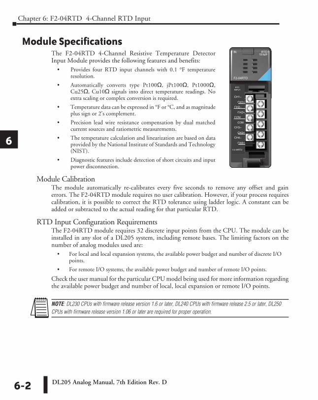
Module SpecificationsThe F2-04RTD 4-Channel Resistive Temperature Detector Input Module provides the following features and benefits:
• Provides four RTD input channels with 0.1 °F temperature resolution.
• Automatically converts type Pt100q, jPt100q, Pt1000q, Cu25q, Cu10q signals into direct temperature readings. No extra scaling or complex conversion is required.
• Temperature data can be expressed in °F or °C, and as magnitude plus sign or 2’s complement.
• Precision lead wire resistance compensation by dual matched current sources and ratiometric measurements.
• The temperature calculation and linearization are based on data provided by the National Institute of Standards and Technology (NIST).
• Diagnostic features include detection of short circuits and input power disconnection.
Module CalibrationThe module automatically re-calibrates every five seconds to remove any offset and gain errors. The F2-04RTD module requires no user calibration. However, if your process requires calibration, it is possible to correct the RTD tolerance using ladder logic. A constant can be added or subtracted to the actual reading for that particular RTD.
RTD Input Configuration RequirementsThe F2-04RTD module requires 32 discrete input points from the CPU. The module can be installed in any slot of a DL205 system, including remote bases. The limiting factors on the number of analog modules used are:
• For local and local expansion systems, the available power budget and number of discrete I/O points.
• For remote I/O systems, the available power budget and number of remote I/O points.
Check the user manual for the particular CPU model being used for more information regarding the available power budget and number of local, local expansion or remote I/O points.
NOTE: DL230 CPUs with firmware release version 1.6 or later, DL240 CPUs with firmware release 2.5 or later, DL250 CPUs with firmware release version 1.06 or later are required for proper operation.
CH1+
CH2+
COM
CH3+
CH4+
CH1–
CH2–
COM
CH3–
CH4–
F2-04RTD
IN RTDTEMP
RTDINPUT
F2-04RTD
+CH1+
+CH2+
COM
+CH3+
+CH4+
CH1–
CH2–
COM
CH3–
CH4–
F2-04RTD
IN
RTDINPUT
F2-04RTD
RTDTEMP
DL205 Analog Manual, 7th Edition Rev. D 6-3
Chapter 6: F2-04RTD 4-Channel RTD Input
1
2
3
4
5
6
7
8
9
10
11
12
13
14
A
B
C
D
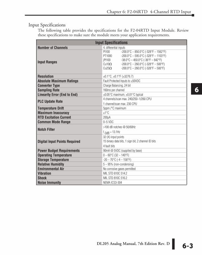
Input SpecificationsThe following table provides the specifications for the F2-04RTD Input Module. Review these specifications to make sure the module meets your application requirements. 1
2
3
4
5
6
7
8
9
10
11
12
13
14
A
B
C
D
Input Specifications Number of Channels 4, differential inputs
Input Ranges
Pt100 -200.0°C – 850.0°C (-328°F – 1562°F) PT1000 -200.0°C – 595.0°C (-328°F – 1103°F) jPt100 -38.0°C – 450.0°C (-36°F – 842°F) Cu10q -200.0°C – 260.0°C (-328°F – 500°F) Cu25q -200.0°C – 260.0°C (-328°F – 500°F)
Resolution ±0.1°C, ±0.1°F (±3276.7) Absolute Maximum Ratings Fault Protected Inputs to ±50VDC Converter Type Charge Balancing, 24 bit Sampling Rate 160ms per channel Linearity Error (End to End) ±0.05°C maximum, ±0.01°C typical
PLC Update Rate 4 channels/scan max. 240/250–1/260 CPU 1 channel/scan max. 230 CPU
Temperature Drift 5ppm /°C maximum Maximum Inaccuracy ±1°C RTD Excitation Current 200µA Common Mode Range 0–5 VDC
Notch Filter >100 dB notches @ 50/60Hz f-3dB = 13.1Hz
Digital Input Points Required 32 (X) input points 15 binary data bits, 1 sign bit, 2 channel ID bits 4 fault bits
Power Budget Requirements 90mA @ 5VDC (supplied by base) Operating Temperature 0 – 60°C (32 – 140°F) Storage Temperature -20 – 70°C (-4 – 158°F) Relative Humidity 5 – 95% (non-condensing) Environmental Air No corrosive gases permitted Vibration MIL STD 810C 514.2 Shock MIL STD 810C 516.2 Noise Immunity NEMA ICS3-304
DL205 Analog Manual, 7th Edition Rev. D6-4
Chapter 6: F2-04RTD 4-Channel RTD Input
1
2
3
4
5
6
7
8
9
10
11
12
13
14
A
B
C
D
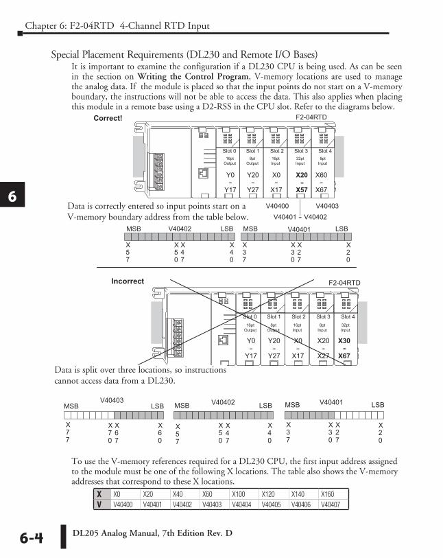
Special Placement Requirements (DL230 and Remote I/O Bases)It is important to examine the configuration if a DL230 CPU is being used. As can be seen in the section on Writing the Control Program, V-memory locations are used to manage the analog data. If the module is placed so that the input points do not start on a V-memory boundary, the instructions will not be able to access the data. This also applies when placing this module in a remote base using a D2-RSS in the CPU slot. Refer to the diagrams below.
To use the V-memory references required for a DL230 CPU, the first input address assigned to the module must be one of the following X locations. The table also shows the V-memory addresses that correspond to these X locations.
1
2
3
4
5
6
7
8
9
10
11
12
13
14
A
B
C
D X X0 X20 X40 X60 X100 X120 X140 X160 V V40400 V40401 V40402 V40403 V40404 V40405 V40406 V40407
X37
F2-04RTD
V40401 -- V40402
BSLBSM
X20
V40400 V40403
Correct!
16ptOutput
8ptOutput
32ptInput Input
8pt16ptInput
Y0--
Y17
Y20--
Y27
X0--
X17
X20--
X57
X60--
X67
Slot 0 Slot 1 Slot 2 Slot 3 Slot 4
X27
X30
X57
MSB
X40
X47
X50
LSBV40402 V40401
Data is correctly entered so input points start on a V-memory boundary address from the table below.
16ptOutput
8ptOutput
8ptInput Input
32pt16ptInput
Y0--
Y17
Y20--
Y27
X0--
X17
X20--
X27
X30--
X67
F2-04RTD
V40402 BSLBSM
X40
X60
X47
X50
V40401 BSLBSM
X20
X37
X27
X30
Incorrect
Slot 0 Slot 1 Slot 2 Slot 3 Slot 4
MSB
X77
V40403
X67
X70
LSB
X57
Data is split over three locations, so instructions cannot access data from a DL230.
DL205 Analog Manual, 7th Edition Rev. D 6-5
Chapter 6: F2-04RTD 4-Channel RTD Input
1
2
3
4
5
6
7
8
9
10
11
12
13
14
A
B
C
D
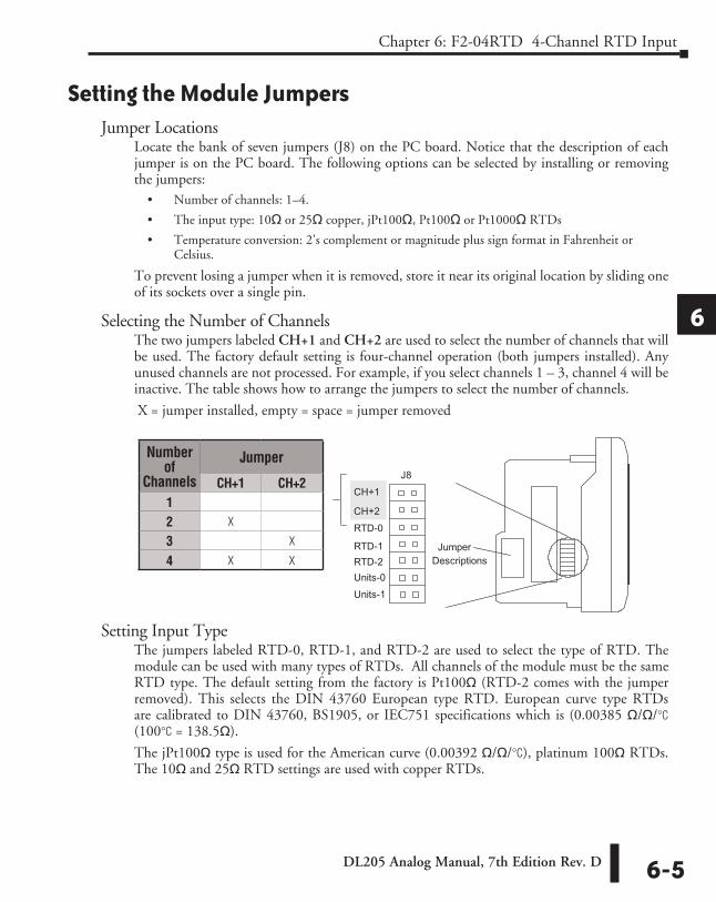
Setting the Module JumpersJumper Locations
Locate the bank of seven jumpers (J8) on the PC board. Notice that the description of each jumper is on the PC board. The following options can be selected by installing or removing the jumpers:
• Number of channels: 1–4.
• The input type: 10q or 25q copper, jPt100q, Pt100q or Pt1000q RTDs
• Temperature conversion: 2’s complement or magnitude plus sign format in Fahrenheit or Celsius.
To prevent losing a jumper when it is removed, store it near its original location by sliding one of its sockets over a single pin.
Selecting the Number of ChannelsThe two jumpers labeled CH+1 and CH+2 are used to select the number of channels that will be used. The factory default setting is four-channel operation (both jumpers installed). Any unused channels are not processed. For example, if you select channels 1 – 3, channel 4 will be inactive. The table shows how to arrange the jumpers to select the number of channels.
X = jumper installed, empty = space = jumper removed
Setting Input TypeThe jumpers labeled RTD-0, RTD-1, and RTD-2 are used to select the type of RTD. The module can be used with many types of RTDs. All channels of the module must be the same RTD type. The default setting from the factory is Pt100q (RTD-2 comes with the jumper removed). This selects the DIN 43760 European type RTD. European curve type RTDs are calibrated to DIN 43760, BS1905, or IEC751 specifications which is (0.00385 q/q/°C (100°C = 138.5q).
The jPt100q type is used for the American curve (0.00392 q/q/°C), platinum 100q RTDs. The 10q and 25q RTD settings are used with copper RTDs.
1
2
3
4
5
6
7
8
9
10
11
12
13
14
A
B
C
D
Jumper
Units-1
Units-0RTD-2RTD-1
RTD-0
CH+2
CH+1
J8
Descriptions
Number of
Channels
Jumper
CH+1 CH+212 X
3 X
4 X X
DL205 Analog Manual, 7th Edition Rev. D6-6
Chapter 6: F2-04RTD 4-Channel RTD Input
1
2
3
4
5
6
7
8
9
10
11
12
13
14
A
B
C
D
The table shows how to arrange the jumpers to set the input type.
X = jumper installed, empty space = jumper removed.
Selecting the Conversion UnitsUse the last two jumpers, Units-0 and Unit-1, to set the conversion unit. The options are magnitude + sign or 2’s complement in Fahrenheit or Celsius. The module comes from the factory with both jumpers installed for magnitude + sign conversion in Fahrenheit.
All RTD types are converted into a direct temperature reading in either Fahrenheit or Celsius. The data contains one implied decimal place. For example, a value in V-memory of 1002 would be 100.2°C or °F.
Negative temperatures can be represented in either 2’s complement or magnitude plus sign form. If the temperature is negative, the most significant bit in the V-memory location is set (X17).
The 2’s complement data format may be required to correctly display bipolar data on some operator interfaces. This data format could also be used to simplify averaging a bipolar signal. To view this data format in DirectSoft, select Signed Decimal.
The table shows how to arrange the jumpers.
X = jumper installed, empty space = jumper removed.
1
2
3
4
5
6
7
8
9
10
11
12
13
14
A
B
C
D
RTD InputsJumper Pins
RTD-0 RTD-1 RTD-2Cu 10 qCu 25 q X
jPt100 q X
Pt100 q X X
Pt1000 q X
Number of
Channels
Temperature Conversion UnitsMagnitude + Sign
°F °C2’s Compliment °F °C
Units-0 X X
Units-1 X X
DL205 Analog Manual, 7th Edition Rev. D 6-7
Chapter 6: F2-04RTD 4-Channel RTD Input
1
2
3
4
5
6
7
8
9
10
11
12
13
14
A
B
C
D
Connecting the Field WiringWiring Guidelines
Your company may have guidelines for wiring and cable installation. If so, check the guidelines before beginning the installation. Here are some general things to consider:
• Use the shortest wiring route whenever possible.
• Use shielded wiring and ground the shield at the transmitter source. Do not ground the shield at both the module and the source.
• Do not run the signal wiring next to large motors, high current switches, or transformers. This may cause noise problems.
• Route the wiring through an approved cable housing to minimize the risk of accidental damage. Check local and national codes to choose the correct method for your application.
To remove the terminal block, disconnect power to the PLC and the field devices. Pull the terminal block firmly until the connector separates from the module.
You can remove the RTD module from the PLC by folding out the retaining tabs at the top and bottom of the module. As the retaining tabs pivot upward and outward, the module’s connector is lifted out of the PLC socket. Once the connector is free, you can lift the module out of its slot.
Use the following diagram to connect the field wiring. If necessary, the F2–04RTD terminal block can be removed to make removal of the module possible without disturbing field wiring.
RTD - Resistance Temperature DetectorUse shielded RTDs whenever possible to minimize noise on the input signal. Ground the shield wire at one end only, preferably at the RTD source.
Lead Configuration for RTD Sensors
The suggested three-lead configuration shown below provides one lead to the CH+ terminal, one lead to the CH– terminal, and one lead to the common terminal. Compensation circuitry nulls out the lead length for accurate temperature measurements.
Some sensors have four leads. When making connections, do not connect the second lead to the CH+ input; leave that lead unconnected.
1
2
3
4
5
6
7
8
9
10
11
12
13
14
A
B
C
D
Red
Red
WhiteWhite (if applicable)
To CH--
To CH+
Wiring Connections For Typical RTD Sensor
Sensor
(if sensor has 4 leads, onlyconnect one lead to CH+)
No Connection
To COM
Do not use configurations that lack the use of the same color lead to both the CH– and COM terminals. There is no compensation and temperature readings will be inaccurate.
This module has low RTD excitation current, the worse case dissipation with 100q RTDs connected is only 0.016 mW.
DL205 Analog Manual, 7th Edition Rev. D6-8
Chapter 6: F2-04RTD 4-Channel RTD Input
1
2
3
4
5
6
7
8
9
10
11
12
13
14
A
B
C
D
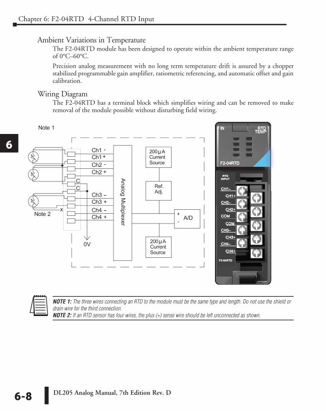
Ambient Variations in TemperatureThe F2-04RTD module has been designed to operate within the ambient temperature range of 0°C–60°C.
Precision analog measurement with no long term temperature drift is assured by a chopper stabilized programmable gain amplifier, ratiometric referencing, and automatic offset and gain calibration.
Wiring DiagramThe F2-04RTD has a terminal block which simplifies wiring and can be removed to make removal of the module possible without disturbing field wiring.
NOTE 1: The three wires connecting an RTD to the module must be the same type and length. Do not use the shield or drain wire for the third connection. NOTE 2: If an RTD sensor has four wires, the plus (+) sense wire should be left unconnected as shown.
1
2
3
4
5
6
7
8
9
10
11
12
13
14
A
B
C
D
A/D+-
Ch1
Ch2
Ch3 --
Ch4 --
Ch1+
Ch2 +
Ch3 +
Ch4 +
CC
200 ACurrentSource
200 ACurrentSource
Ref.Adj.
xNote 2
Note 1
-
-
0V
Analog M
ultiplexerCH1+
CH2+
COM
CH3+
CH4+
CH1–
CH2–
COM
CH3–
CH4–
F2-04RTD
IN RTDTEMP
RTDINPUT
F2-04RTD
CH1+CH1+
CH2+CH2+
COM
CH3+CH3+
CH4+CH4+
CH1–
CH2–
COM
CH3–
CH4–
F2-04RTD
IN
RTDINPUT
F2-04RTD
RTDTEMP
μ
μ
DL205 Analog Manual, 7th Edition Rev. D 6-9
Chapter 6: F2-04RTD 4-Channel RTD Input
1
2
3
4
5
6
7
8
9
10
11
12
13
14
A
B
C
D
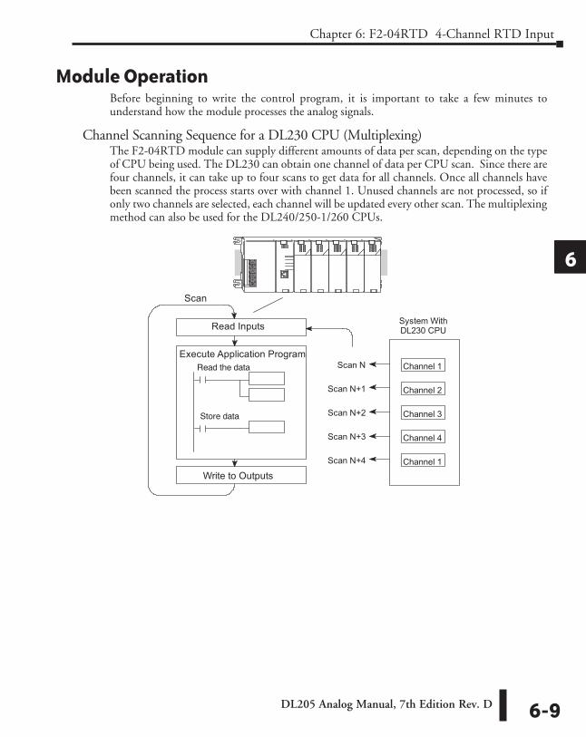
Module OperationBefore beginning to write the control program, it is important to take a few minutes to understand how the module processes the analog signals.
Channel Scanning Sequence for a DL230 CPU (Multiplexing)The F2-04RTD module can supply different amounts of data per scan, depending on the type of CPU being used. The DL230 can obtain one channel of data per CPU scan. Since there are four channels, it can take up to four scans to get data for all channels. Once all channels have been scanned the process starts over with channel 1. Unused channels are not processed, so if only two channels are selected, each channel will be updated every other scan. The multiplexing method can also be used for the DL240/250-1/260 CPUs.
1
2
3
4
5
6
7
8
9
10
11
12
13
14
A
B
C
D
Channel 1Scan NRead the data
Store data
Read Inputs
Execute Application Program
Channel 2Scan N+1
Channel 3Scan N+2
Channel 4Scan N+3
Channel 1Scan N+4
Scan
Write to Outputs
System WithDL230 CPU
DL205 Analog Manual, 7th Edition Rev. D6-10
Chapter 6: F2-04RTD 4-Channel RTD Input
1
2
3
4
5
6
7
8
9
10
11
12
13
14
A
B
C
D
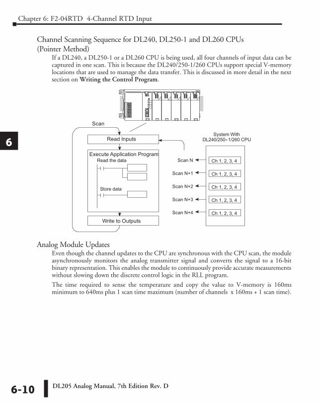
Channel Scanning Sequence for DL240, DL250-1 and DL260 CPUs (Pointer Method)
If a DL240, a DL250-1 or a DL260 CPU is being used, all four channels of input data can be captured in one scan. This is because the DL240/250-1/260 CPUs support special V-memory locations that are used to manage the data transfer. This is discussed in more detail in the next section on Writing the Control Program.
Analog Module UpdatesEven though the channel updates to the CPU are synchronous with the CPU scan, the module asynchronously monitors the analog transmitter signal and converts the signal to a 16-bit binary representation. This enables the module to continuously provide accurate measurements without slowing down the discrete control logic in the RLL program.
The time required to sense the temperature and copy the value to V-memory is 160ms minimum to 640ms plus 1 scan time maximum (number of channels x 160ms + 1 scan time).
1
2
3
4
5
6
7
8
9
10
11
12
13
14
A
B
C
D
Read the data
Store data
Read Inputs
Execute Application Program
Scan
Write to Outputs
Ch 1, 2, 3, 4Scan N
Scan N+1
Scan N+2
Scan N+3
Scan N+4
Ch 1, 2, 3, 4
Ch 1, 2, 3, 4
Ch 1, 2, 3, 4
Ch 1, 2, 3, 4
System WithDL240/250--1/260 CPU
DL205 Analog Manual, 7th Edition Rev. D 6-11
Chapter 6: F2-04RTD 4-Channel RTD Input
1
2
3
4
5
6
7
8
9
10
11
12
13
14
A
B
C
D
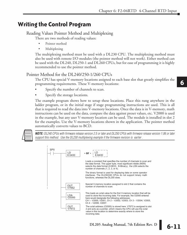
Writing the Control ProgramReading Values Pointer Method and Multiplexing
There are two methods of reading values:• Pointer method
• Multiplexing
The multiplexing method must be used with a DL230 CPU. The multiplexing method must also be used with remote I/O modules (the pointer method will not work). Either method can be used with the DL240, DL250-1 and DL260 CPUs, but for ease of programming it is highly recommended to use the pointer method.
Pointer Method for the DL240/250-1/260 CPUsThe CPU has special V-memory locations assigned to each base slot that greatly simplifies the programming requirements. These V-memory locations:
• Specify the number of channels to scan.
• Specify the storage locations.
The example program shows how to setup these locations. Place this rung anywhere in the ladder program, or in the initial stage if stage programming instructions are used. This is all that is required to read the data into V-memory locations. Once the data is in V-memory, math instructions can be used on the data, compare the data against preset values, etc. V2000 is used in the example, but any user V-memory location can be used. The module is installed in slot 2 for the examples. Use the V-memory locations shown in the application. The pointer method automatically converts values to BCD.
NOTE: DL240 CPUs with firmware release version 2.5 or later and DL250 CPUs with firmware release version 1.06 or later support this method. Use the DL230 multiplexing example if the firmware revision is earlier .
1
2
3
4
5
6
7
8
9
10
11
12
13
14
A
B
C
D
SP0LDK
LDAO2000
OUTV7672
This loads an octal value for the first V-memory location that will beused to store the incoming data. For example, the O2000 enteredhere would designate the following addresses:Ch1 -- V2000, V2001, Ch 2 -- V2002, V2003, Ch 3 -- V2004, V2005,Ch 4 -- V2006, V2007.The octal address (O2000) is stored here. V7672 is assigned to slot2 and acts as a pointer, which means the CPU will use the octalvalue in this location to determine exactly where to store theincoming data.
OUTV7662
Special V-memory location assigned to slot 2 that contains thenumber of channels to scan.
00LD
Loads a constant that specifies the number of channels to scan andthe data format. The upper byte, most significant nibble (MSN)selects the data format (0=BCD, 8=Binary), the LSN selects thenumber of channels (1, 2, 3, or 4).
- or -
The binary format is used for displaying data on some operatorinterfaces. The DL230/240 CPUs do not support binary mathfunctions, whereas the DL250 does.
04 K 0084
DL205 Analog Manual, 7th Edition Rev. D6-12
Chapter 6: F2-04RTD 4-Channel RTD Input
1
2
3
4
5
6
7
8
9
10
11
12
13
14
A
B
C
D
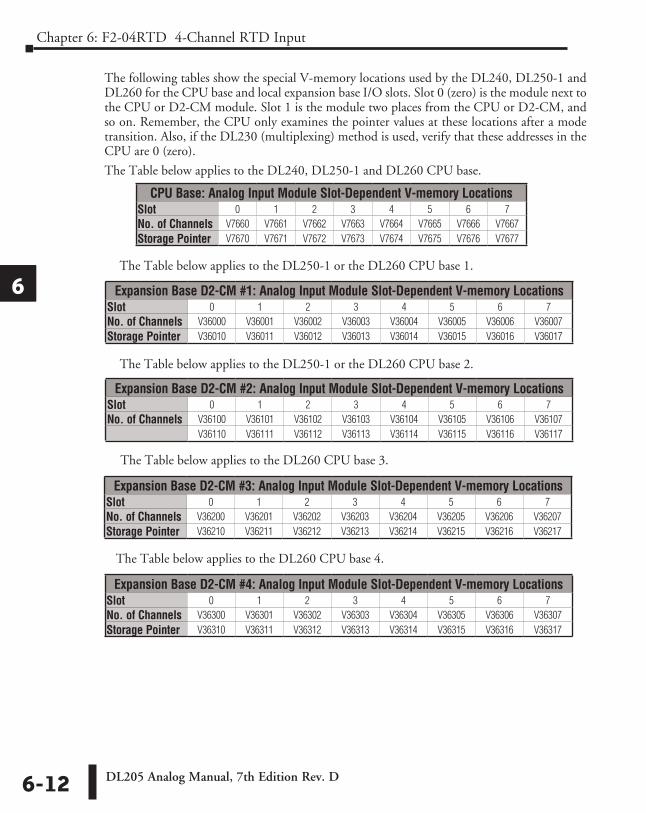
The following tables show the special V-memory locations used by the DL240, DL250-1 and DL260 for the CPU base and local expansion base I/O slots. Slot 0 (zero) is the module next to the CPU or D2-CM module. Slot 1 is the module two places from the CPU or D2-CM, and so on. Remember, the CPU only examines the pointer values at these locations after a mode transition. Also, if the DL230 (multiplexing) method is used, verify that these addresses in the CPU are 0 (zero).
The Table below applies to the DL240, DL250-1 and DL260 CPU base.
1
2
3
4
5
6
7
8
9
10
11
12
13
14
A
B
C
D
CPU Base: Analog Input Module Slot-Dependent V-memory LocationsSlot 0 1 2 3 4 5 6 7No. of Channels V7660 V7661 V7662 V7663 V7664 V7665 V7666 V7667Storage Pointer V7670 V7671 V7672 V7673 V7674 V7675 V7676 V7677
Expansion Base D2-CM #1: Analog Input Module Slot-Dependent V-memory LocationsSlot 0 1 2 3 4 5 6 7No. of Channels V36000 V36001 V36002 V36003 V36004 V36005 V36006 V36007Storage Pointer V36010 V36011 V36012 V36013 V36014 V36015 V36016 V36017
Expansion Base D2-CM #2: Analog Input Module Slot-Dependent V-memory LocationsSlot 0 1 2 3 4 5 6 7No. of Channels V36100 V36101 V36102 V36103 V36104 V36105 V36106 V36107
V36110 V36111 V36112 V36113 V36114 V36115 V36116 V36117
Expansion Base D2-CM #3: Analog Input Module Slot-Dependent V-memory LocationsSlot 0 1 2 3 4 5 6 7No. of Channels V36200 V36201 V36202 V36203 V36204 V36205 V36206 V36207Storage Pointer V36210 V36211 V36212 V36213 V36214 V36215 V36216 V36217
Expansion Base D2-CM #4: Analog Input Module Slot-Dependent V-memory LocationsSlot 0 1 2 3 4 5 6 7No. of Channels V36300 V36301 V36302 V36303 V36304 V36305 V36306 V36307Storage Pointer V36310 V36311 V36312 V36313 V36314 V36315 V36316 V36317
The Table below applies to the DL250-1 or the DL260 CPU base 1.
The Table below applies to the DL250-1 or the DL260 CPU base 2.
The Table below applies to the DL260 CPU base 3.
The Table below applies to the DL260 CPU base 4.
DL205 Analog Manual, 7th Edition Rev. D 6-13
Chapter 6: F2-04RTD 4-Channel RTD Input
1
2
3
4
5
6
7
8
9
10
11
12
13
14
A
B
C
D
Negative Temperature Readings with Magnitude Plus Sign for the DL240, DL250-1 and DL260 CPUs (Pointer Method)
With bipolar ranges, some additional logic will be needed to determine whether the value being returned represents a positive voltage or a negative voltage. For example, the direction for a motor might need to be known. There is a solution for this:
• If bipolar ranges are used and a value greater than or equal to 8000hex is obtained, the value is negative.
• If a value less than or equal to 7FFFhex is obtained, then the value is positive.
The sign bit is the most significant bit, which combines 8000hex to the data value. If the value is greater than or equal to 8000hex, only the most significant bit and the active channel bits need to be masked to determine the actual data value.
NOTE: DL240 CPUs with firmware release version 2.5 or later and DL250 CPUs with firmware release version 1.06 or later support this method. Use the DL230 multiplexing example if your firmware is an earlier version.
The two programs on the next page show how this can be accomplished. The first example uses magnitude plus sign (binary) and the second example uses magnitude plus sign (BCD). The examples only show two channels.
It is good to know when a value is negative, so these rungs should be placed before any other operations that use the data, such as math instructions, scaling operations, etc. Also, if stage programming instructions are being used, these rungs should be in a stage that is always active.
NOTE: This logic is only needed for each channel that is using bipolar input signals.
1
2
3
4
5
6
7
8
9
10
11
12
13
14
A
B
C
D
DL205 Analog Manual, 7th Edition Rev. D6-14
Chapter 6: F2-04RTD 4-Channel RTD Input
1
2
3
4
5
6
7
8
9
10
11
12
13
14
A
B
C
D
Magnitude Plus Sign (Binary)
Magnitude Plus Sign (BCD)
1
2
3
4
5
6
7
8
9
10
11
12
13
14
A
B
C
D
SP1
OUTC1
LDV2000
OUTV2010
Load channel 1 data from V-memory into theaccumulator. Contact SP1 is always on.
Put the actual signal value in V2010. Now you can usethe data normally.
ANDDK7FFF
This instruction masks the sign bit of the binary data, ifit is set. Without this step, negative values will not becorrect so do not forget to include it.
V2000 K8000Channel 1 data is negative when C1 is on (a value of--1.0 reads as 8010, --2.0 is 8020, etc.).
SP1
OUTC2
LDV2002
OUTV2012
Load channel 2 from V-memory into the accumulator.Contact SP1 is always on.
Put the actual signal value in V2012. Now you can usethe data normally.
ANDDK7FFF
This instruction masks the sign bit of the binary data, ifit is set. Without this step, negative values will not becorrect so do not forget to include it.
V2002 K8000Channel 2 data is negative when C2 is on (a value of--1.0 reads as 8010, --2.0 is 8020, etc.).
²
²
Check Channel 1
Check Channel 2
SP1
OUTC1
LDDV2000
OUTDV2010
Load channel 1 data from V-memory into theaccumulator. Remember, the data can be negative.Contact SP1 is always on.
Put the actual signal value in V2010. Now you can usethe data normally.
ANDDK7FFFFFFF
This instruction masks the sign bit of the BCD data, if itis set. Without this step, negative values will not becorrect so do not forget to include it.
V2001 K8000
Check Channel 1
Check Channel 2
Channel 1 data is negative when C1 is on (a value of--1.0 reads as 8000 0010, --2.0 is 8000 0020, etc.).
SP1
OUTC2
LDDV2002
OUTDV2012
Load channel 2 from V-memory into the accumulator.Remember, the data can be negative. Contact SP1 isalways on.
Put the actual signal value in V2012. Now you can usethe data normally.
ANDDK7FFFFFFF
This instruction masks the sign bit of the BCD data, if itis set. Without this step, negative values will not becorrect so do not forget to include it.
V2003 K8000Channel 2 data is negative when C2 is on (a value of--1.0 reads as 8000 0010, --2.0 is 8000 0020, etc.).
²
²
DL205 Analog Manual, 7th Edition Rev. D 6-15
Chapter 6: F2-04RTD 4-Channel RTD Input
1
2
3
4
5
6
7
8
9
10
11
12
13
14
A
B
C
D
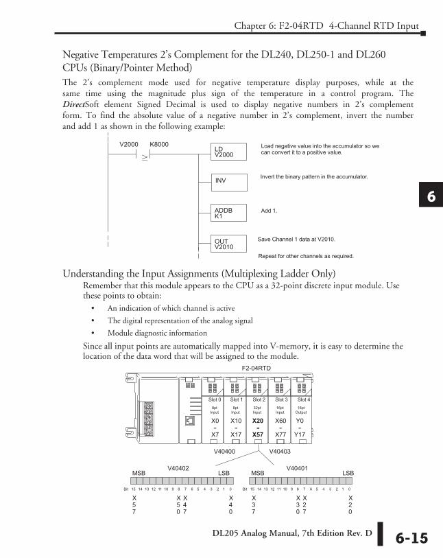
Negative Temperatures 2’s Complement for the DL240, DL250-1 and DL260 CPUs (Binary/Pointer Method)The 2’s complement mode used for negative temperature display purposes, while at the same time using the magnitude plus sign of the temperature in a control program. The DirectSoft element Signed Decimal is used to display negative numbers in 2’s complement form. To find the absolute value of a negative number in 2’s complement, invert the number and add 1 as shown in the following example:
Understanding the Input Assignments (Multiplexing Ladder Only)Remember that this module appears to the CPU as a 32-point discrete input module. Use these points to obtain:
• An indication of which channel is active
• The digital representation of the analog signal
• Module diagnostic information
Since all input points are automatically mapped into V-memory, it is easy to determine the location of the data word that will be assigned to the module.
1
2
3
4
5
6
7
8
9
10
11
12
13
14
A
B
C
D
LDV2000
OUTV2010
ADDBK1
V2000 K8000
²
INV
Load negative value into the accumulator so wecan convert it to a positive value.
Invert the binary pattern in the accumulator.
Add 1.
Save Channel 1 data at V2010.
Repeat for other channels as required.
F2-04RTD
V40400 V40403
8ptInput
8ptInput
16ptInput Output
16pt32ptInput
X0--
X7
X10--
X17
X20--
X57
X60--
X77
Y0--
Y17
Slot 0 Slot 1 Slot 2 Slot 3 Slot 4
X37
V40401BSLBSM
X20
X27
X30
X57
V40402BSLBSM
X40
X47
X50
0134567891011121314 251Bit 0134567891011121314 251Bit
DL205 Analog Manual, 7th Edition Rev. D6-16
Chapter 6: F2-04RTD 4-Channel RTD Input
1
2
3
4
5
6
7
8
9
10
11
12
13
14
A
B
C
D
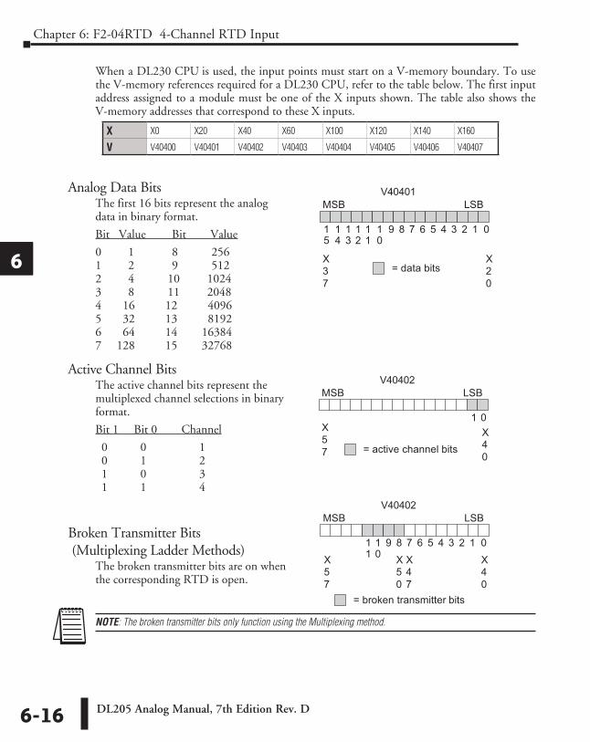
When a DL230 CPU is used, the input points must start on a V-memory boundary. To use the V-memory references required for a DL230 CPU, refer to the table below. The first input address assigned to a module must be one of the X inputs shown. The table also shows the V-memory addresses that correspond to these X inputs.
Analog Data BitsThe first 16 bits represent the analog data in binary format.
Bit Value Bit Value
0 1 8 256 1 2 9 512 2 4 10 1024 3 8 11 2048 4 16 12 4096 5 32 13 8192 6 64 14 16384 7 128 15 32768
Active Channel BitsThe active channel bits represent the multiplexed channel selections in binary format.
Bit 1 Bit 0 Channel
0 0 1 0 1 2 1 0 3 1 1 4
Broken Transmitter Bits (Multiplexing Ladder Methods)
The broken transmitter bits are on when the corresponding RTD is open.
NOTE: The broken transmitter bits only function using the Multiplexing method.
1
2
3
4
5
6
7
8
9
10
11
12
13
14
A
B
C
D
X X0 X20 X40 X60 X100 X120 X140 X160
V V40400 V40401 V40402 V40403 V40404 V40405 V40406 V40407
V40401BSLBSM
011
10
9 8 7 6 5 4 3 2 1
= data bitsX20
X37
12
13
14
15
V40402BSLBSM
01
= active channel bitsX40
X57
V40402BSLBSM
011
10
9 8 7 6 5 4 3 2 1
= broken transmitter bits
X40
X57
X47
X50
DL205 Analog Manual, 7th Edition Rev. D 6-17
Chapter 6: F2-04RTD 4-Channel RTD Input
1
2
3
4
5
6
7
8
9
10
11
12
13
14
A
B
C
D
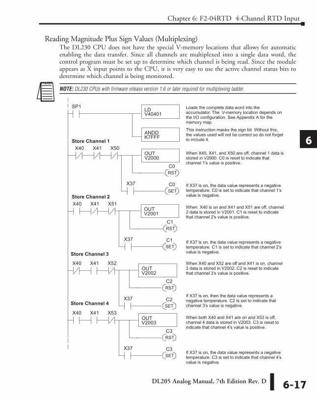
Reading Magnitude Plus Sign Values (Multiplexing)The DL230 CPU does not have the special V-memory locations that allows for automatic enabling the data transfer. Since all channels are multiplexed into a single data word, the control program must be set up to determine which channel is being read. Since the module appears as X input points to the CPU, it is very easy to use the active channel status bits to determine which channel is being monitored.
NOTE: DL230 CPUs with firmware release version 1.6 or later required for multiplexing ladder.
1
2
3
4
5
6
7
8
9
10
11
12
13
14
A
B
C
D
This instruction masks the sign bit. Without this,the values used will not be correct so do not forgetto include it.
Loads the complete data word into theaccumulator. The V-memory location depends onthe I/O configuration. See Appendix A for thememory map.
LDV40401
ANDDK7FFF
SP1
X40 X41 X50Store Channel 1
OUTV2000
When X40, X41, and X50 are off, channel 1 data isstored in V2000. C0 is reset to indicate thatchannel 1’s value is positive.
SETC0X37
RSTC0
If X37 is on, the data value represents a negativetemperature. C0 is set to indicate that channel 1’svalue is negative.
X40 X41 X51Store Channel 2
OUTV2001
When X40 is on and X41 and X51 are off, channel2 data is stored in V2001. C1 is reset to indicatethat channel 2’s value is positive.
SETC1X37
RSTC1
If X37 is on, the data value represents a negativetemperature. C1 is set to indicate that channel 2’svalue is negative.
X40 X41 X52OUTV2002
SETC2X37
RSTC2
X40 X41 X53OUTV2003
SETC3X37
RSTC3
When X40 and X52 are off and X41 is on, channel3 data is stored in V2002. C2 is reset to indicatethat channel 3’s value is positive.
If X37 is on, then the data value represents anegative temperature. C2 is set to indicate thatchannel 3’s value is negative.
When both X40 and X41 are on and X53 is off,channel 4 data is stored in V2003. C3 is reset toindicate that channel 4’s value is positive.
If X37 is on, the data value represents a negativetemperature. C3 is set to indicate that channel 4’svalue is negative.
Store Channel 3
Store Channel 4
DL205 Analog Manual, 7th Edition Rev. D6-18
Chapter 6: F2-04RTD 4-Channel RTD Input
1
2
3
4
5
6
7
8
9
10
11
12
13
14
A
B
C
D
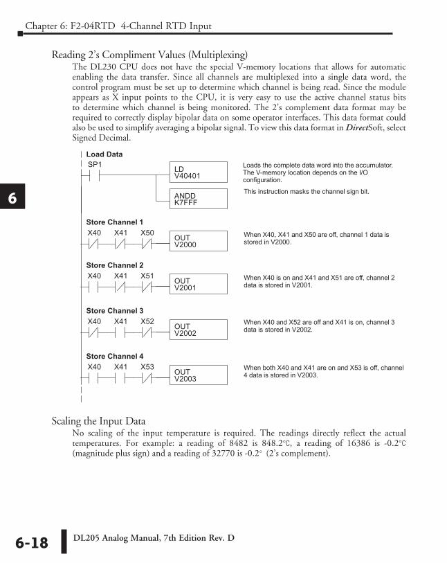
Reading 2’s Compliment Values (Multiplexing)The DL230 CPU does not have the special V-memory locations that allows for automatic enabling the data transfer. Since all channels are multiplexed into a single data word, the control program must be set up to determine which channel is being read. Since the module appears as X input points to the CPU, it is very easy to use the active channel status bits to determine which channel is being monitored. The 2’s complement data format may be required to correctly display bipolar data on some operator interfaces. This data format could also be used to simplify averaging a bipolar signal. To view this data format in DirectSoft, select Signed Decimal.
Scaling the Input DataNo scaling of the input temperature is required. The readings directly reflect the actual temperatures. For example: a reading of 8482 is 848.2°C, a reading of 16386 is -0.2°C (magnitude plus sign) and a reading of 32770 is -0.2° (2’s complement).
1
2
3
4
5
6
7
8
9
10
11
12
13
14
A
B
C
D
This instruction masks the channel sign bit.
Loads the complete data word into the accumulator.The V-memory location depends on the I/Oconfiguration.
Load Data
LDV40401
ANDDK7FFF
SP1
X40 X41 X50Store Channel 1
OUTV2000
When X40, X41 and X50 are off, channel 1 data isstored in V2000.
When X40 is on and X41 and X51 are off, channel 2data is stored in V2001.
When X40 and X52 are off and X41 is on, channel 3data is stored in V2002.
When both X40 and X41 are on and X53 is off, channel4 data is stored in V2003.
X40 X41 X51Store Channel 2
OUTV2001
X40 X41 X52Store Channel 3
OUTV2002
X40 X41 X53Store Channel 4
OUTV2003
DL205 Analog Manual, 7th Edition Rev. D 6-19
Chapter 6: F2-04RTD 4-Channel RTD Input
1
2
3
4
5
6
7
8
9
10
11
12
13
14
A
B
C
D
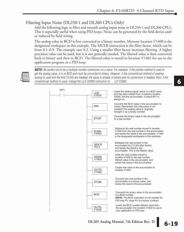
Filtering Input Noise (DL250-1 and DL260 CPUs Only)Add the following logic to filter and smooth analog input noise in DL250-1 and DL260 CPUs. This is especially useful when using PID loops. Noise can be generated by the field device and/or induced by field wiring.
The analog value in BCD is first converted to a binary number. Memory location V1400 is the designated workspace in this example. The MULR instruction is the filter factor, which can be from 0.1–0.9. The example uses 0.2. Using a smaller filter factor increases filtering. A higher precision value can be used, but it is not generally needed. The filtered value is then converted back to binary and then to BCD. The filtered value is stored in location V1402 for use in the application program or a PID loop.
NOTE: Be careful not to do a multiple number conversion on a value. For example, if the pointer method is used to get the analog value, it is in BCD and must be converted to binary. However, if the conventional method of reading analog is used and the first 15 bits are masked, the value is already in binary and no conversion is needed. Also, if the conventional method is used, change the LLD V2000 instruction to LD V2000.
1
2
3
4
5
6
7
8
9
10
11
12
13
14
A
B
C
D
LDDV2000
SUBRV1400
BTOR
SP1
BIN
Loads the analog signal, which is a BCD valueand has been loaded from V-memory locationV2000, into the accumulator. Contact SP1 isalways on.
Converts the BCD value in the accumulator tobinary. Remember, this instruction is notneeded if the analog value is originallybrought in as a binary number.
Converts the binary value in the accumulatorto a real number.
Subtracts the real number stored in locationV1400 from the real number in the accumulator,and stores the result in the accumulator. V1400is the designated workspace in this example.
Multiplies the real number in theaccumulator by 0.2 (the filter factor),and stores the result in theaccumulator. This is the filtered value.
OUTDV1400
ADDRV1400
MULRR0.2
OUTDV1402
BCD
RTOB
Adds the real number stored inlocation V1400 to the real numberfiltered value in the accumulator, andstores the result in the accumulator.
Copies the value in the accumulator tolocation V1400.
Converts the real number in theaccumulator to a binary value, andstores the result in the accumulator.
Converts the binary value in the accumulatorto a BCD number.NOTE: The BCD instruction is not needed forPID loop PV (loop PV is a binary number).
Loads the BCD number filtered value fromthe accumulator into location V1402 to use inyour application or PID loop.
DL205 Analog Manual, 7th Edition Rev. D6-20
Chapter 6: F2-04RTD 4-Channel RTD Input
1
2
3
4
5
6
7
8
9
10
11
12
13
14
A
B
C
D
Notes
1
2
3
4
5
6
7
8
9
10
11
12
13
14
A
B
C
D


![$YGD GH &iGL] - movilidadgranada.com · f3 f3 f3 f3 f3 f3 f3 f3 f3 f3 f3 f3f3 f3 f3 f3 f3 f3 f3 f3 f3 f3 f3 f3 f3 f3 f3 f3 f3f3 f3 f3 f3 f3 f3 f3 f3 f2 f2 f2 f2 f2 f2 f2 f2 f2 f2](https://img.dokumen.tips/doc/110x75/5bb5162f09d3f2b63a8c0773/ygd-gh-igl-f3-f3-f3-f3-f3-f3-f3-f3-f3-f3-f3-f3f3-f3-f3-f3-f3-f3-f3-f3-f3.jpg)