Embed Size (px)
Citation preview

F i n i s a r
Finisar Corporation 23-November-2011 Rev C7 Page 1
Product Specification
+3200 ps/nm (~200km) DWDM XFP Optical Transceiver
FTLX4213x3xxxx
PRODUCT FEATURES
Supports 10.7Gb/s to 11.35Gb/s
-500 to +3200 ps/nm Dispersion
Tolerance
Supports ITU C & L-Band
DWDM channels
Supports 8x50GHz tuning range
for C-band and 2x200GHz range
for L-Band
Temperature-stabilized DWDM
CMLTM
transmitter
Temperature range: 0°C to 70°C
RoHS-6 Compliant (lead-free)
Power dissipation <4.0W
Adjustable receiver threshold
APPLICATIONS
Amplified DWDM 10Gb/s SONET/SDH
w/FEC
Amplified DWDM 10Gb/s Ethernet
and 10Gb/s Fibre Channel w/FEC
Finisar’s FTLX4213x3xxxx Small Form Factor 10Gb/s (XFP) transceiver complies with
the XFP Multi-Source Agreement (MSA) Specification1. It supports amplified DWDM
10Gb/s SONET/SDH +FEC,10 Gigabit Ethernet +FEC, and 10 Gigabit Fibre Channel
+FEC applications over ~200km of fiber without dispersion compensation. The standard
product supports narrow tunability on the C- and L-Band channels with 50GHz spacing.
Digital diagnostics functions are available via a 2-wire serial interface, as specified in the
XFP MSA. The transceiver is RoHS compliant and lead free per Directive 2002/95/EC3,
and Finisar Application Note AN-20384.
PRODUCT SELECTION
FTLX4213x3xxxx x: tuning range
xxxx: ITU-T Channel#
(see next page)

FTLX4213x3xxxx 3200ps/nm DWDM XFP Product Specification – November 2011 F i n i s a r
Finisar Corporation 23-November-2011 Rev C7 Page 2
C-Band, 8x50GHz XFPs (FTLX4213C3Cxxx)
L-Band, 2x200GHz XFPs (FTLX4213J3Lxxx)
Note* Please contact your Finisar representative for any requirements not
supported by the above channel plan.

FTLX4213x3xxxx 3200ps/nm DWDM XFP Product Specification – November 2011 F i n i s a r
Finisar Corporation 23-November-2011 Rev C7 Page 3
I. Pin Descriptions
Pin Logic Symbol Name/Description Ref.
1 GND Module Ground 1
2 VEE5 Optional –5.2 Power Supply – Not required
3 LVTTL-I Mod-Desel Module De-select; When held low allows the module to
respond to 2-wire serial interface commands
4 LVTTL-O
Interrupt Interrupt (bar); Indicates presence of an important condition
which can be read over the serial 2-wire interface
2
5 LVTTL-I TX_DIS Transmitter Disable; Transmitter laser source turned off
6 VCC5 +5 Power Supply
7 GND Module Ground 1
8 VCC3 +3.3V Power Supply
9 VCC3 +3.3V Power Supply
10 LVTTL-I SCL Serial 2-wire interface clock 2
11 LVTTL-
I/O
SDA Serial 2-wire interface data line 2
12 LVTTL-O Mod_Abs Module Absent; Indicates module is not present. Grounded
in the module.
2
13 LVTTL-O Mod_NR Module Not Ready; Finisar defines it as a logical OR
between RX_LOS and Loss of Lock in TX/RX.
2
14 LVTTL-O RX_LOS Receiver Loss of Signal indicator 2
15 GND Module Ground 1
16 GND Module Ground 1
17 CML-O RD- Receiver inverted data output
18 CML-O RD+ Receiver non-inverted data output
19 GND Module Ground 1
20 VCC2 +1.8V Power Supply – Not required
21 LVTTL-I P_Down/RST Power Down; When high, places the module in the low
power stand-by mode and on the falling edge of P_Down
initiates a module reset
Reset; The falling edge initiates a complete reset of the
module including the 2-wire serial interface, equivalent to a
power cycle.
22 VCC2 +1.8V Power Supply – Not required
23 GND Module Ground 1
24 PECL-I RefCLK+ Reference Clock non-inverted input, AC coupled on the
host board – Not required
25 PECL-I RefCLK- Reference Clock inverted input, AC coupled on the host
board – Not required
26 GND Module Ground 1
27 GND Module Ground 1
28 CML-I TD- Transmitter inverted data input
29 CML-I TD+ Transmitter non-inverted data input
30 GND Module Ground 1
Notes:
1. Module circuit ground is isolated from module chassis ground within the module.
2. Open collector; should be pulled up with 4.7k – 10kohms on host board to a voltage between 3.15V
and 3.6V.

FTLX4213x3xxxx 3200ps/nm DWDM XFP Product Specification – November 2011 F i n i s a r
Finisar Corporation 23-November-2011 Rev C7 Page 4
Diagram of Host Board Connector Block Pin Numbers and Names
II. Absolute Maximum Ratings
Parameter Symbol Min Typ Max Unit Ref.
Maximum Supply Voltage #1 Vcc3 -0.5 4.0 V
Maximum Supply Voltage #2 Vcc5 -0.5 6.0 V
Storage Temperature TS -40 85 C
Case Operating Temperature TOP 0 70 C
Receiver Damage Threshold PRdmg +5 dBm

FTLX4213x3xxxx 3200ps/nm DWDM XFP Product Specification – November 2011 F i n i s a r
Finisar Corporation 23-November-2011 Rev C7 Page 5
III. Electrical Characteristics (TOP = 0 to 70 C, VCC5 = 4.75 to 5.25 Volts)
Parameter Symbol Min Typ Max Unit Ref.
Supply Voltage #1 Vcc5 4.75 5.25 V
Supply Voltage #2 Vcc3 3.13 3.46 V
Supply Current – Vcc5 supply Icc5 500 mA
Supply Current – Vcc3 supply Icc3 750 mA
Module total power P 4.0 W 1
Transmitter
Input differential impedance Rin 100 2
Differential data input swing Vin,pp 120 820 mV
Transmit Disable Voltage VD 2.0 Vcc V 3
Transmit Enable Voltage VEN GND GND+ 0.8 V
Transmit Disable Assert Time 100 us
Receiver
Differential data output swing Vout,pp 340 650 850 mV 4
Data output rise time tr 38 ps 5
Data output fall time tf 38 ps 5
LOS Fault VLOS fault Vcc – 0.5 VccHOST V 6
LOS Normal VLOS norm GND GND+0.5 V 6
Power Supply Rejection PSR See Note 7 below 7
Notes:
1. Maximum total power value is specified across the full temperature and voltage range.
2. After internal AC coupling.
3. Or open circuit.
4. Into 100 ohms differential termination.
5. 20 – 80 %
6. Loss Of Signal is open collector to be pulled up with a 4.7k – 10kohm resistor to 3.15 – 3.6V. Logic 0
indicates normal operation; logic 1 indicates no signal detected.
7. Per Section 2.7.1. in the XFP MSA Specification1.

FTLX4213x3xxxx 3200ps/nm DWDM XFP Product Specification – November 2011 F i n i s a r
Finisar Corporation 23-November-2011 Rev C7 Page 6
IV. Optical Characteristics (EOL, TOP = 0 to 70C, VCC5 = 4.75 to 5.25 Volts)
Transmitter
Parameter Symbol Min Typ Max Unit Ref.
Output Opt. Pwr: 9/125 SMF POUT 0 +4.0 dBm
Optical Extinction Ratio ER 8.2 dB 1
Center Wavelength Spacing 50 GHz 2
Transmitter Center Wavelength –
End Of Life
fc X-5 X X+5 GHz 3
Sidemode Suppression ratio SSRmin 35 dB
Tx Jitter 20kHz-80MHz Txj1 0.3 UI 4,5
Tx Jitter 4MHz – 80MHz Txj2 0.1 UI 4,5
Tx Disable Negate Time tTxE 60 seconds
Relative Intensity Noise RIN -135 dB/Hz
Receiver
Maximum Input Power PMAX -7 dBm
Optical Center Wavelength C 1270 1615 nm
Receiver Reflectance Rrx -27 dB
LOS De-Assert LOSD -30 dBm
LOS Assert LOSA -37 dBm
LOS Hysteresis 0.5 dB
Receiver Sensitivity 6
Data rate
(Gb/s) BER
Dispersion
(ps/nm)
Sensitivity back-to-
back at OSNR>30dB
(dBm)
Sensitivity at -500 to
+3200ps/nm with
OSNR>30dB (dBm)
Threshold
Adjustm.
10.7 1e-4 -500 to +3200 -27 -25 Yes
11.1 1e-4 -500 to +3200 -27 -25 Yes
11.3 1e-4 -500 to +3200 -27 -25 Yes
OSNR Performance 6,7
Data rate
(Gb/s) BER
Dispersion
(ps/nm)
Max OSNR, -500 ps/nm to +3200 ps/nm at Power: -8
to -19dBm (dB)
Threshold
Adjust.
10.7 1e-4 -500 to +3200 19 Yes
11.1 1e-4 -500 to +3200 19 Yes
11.3 1e-4 -500 to +3200 19 Yes
Notes:
1. Measured with unfiltered eye pattern. (without 4th
order Bessel-Thompson Filter)
2. Corresponds to approximately 0.8 nm. Please contact Finisar for 50GHz support.
3. X = Specified ITU Grid frequency. Wavelength stability is achieved within xx seconds of power up.
Please contact Finisar for narrow tunability support.
4. Measured with a host jitter of 50 mUI peak-to-peak.
5. GR-253-CORE Issue 4
6. Measured at 1528-1600nm with worst ER; BER<10-4
; PRBS31.
7. All OSNR measurements are performed with 0.1nm resolution.

FTLX4213x3xxxx 3200ps/nm DWDM XFP Product Specification – November 2011 F i n i s a r
Finisar Corporation 23-November-2011 Rev C7 Page 7
V. General Specifications
Parameter Symbol Min Typ Max Units Ref.
Bit Rate BR 10.7 11.3 Gb/s
Maximum Supported Link Length LMAX 200 km 1
Notes:
1. Distance indicates dispersion budget. Optical amplification is required to achieve maximum distance.
VI. Environmental Specifications
Finisar FTLX4213x3xxxx XFP transceivers have an operating temperature range from
-5°C to +70°C case temperature.
Parameter Symbol Min Typ Max Units Ref.
Case Operating Temperature Top 0 70 °C
Storage Temperature Tsto -40 85 °C
VII. Regulatory Compliance
Finisar FTLX4213x3xxxx XFP transceivers are Class 1 Laser Products. They are
certified per the following standards:
Feature Agency Standard Certificate
Number
Laser Eye
Safety
FDA/CDRH CDRH 21 CFR 1040 and Laser Notice 50 9210176-77
Laser Eye
Safety
TÜV EN 60825-1: 2007, EN60825-2:2004+A1
IEC 60825-1: 2007 (2nd
Edition)
IEC 60825-2: 2010 (3rd
Edition)
72101686
Electrical
Safety
TÜV EN 60950:2006+A11 72101686
Electrical
Safety
UL/CSA
CLASS 3862.07
CLASS 3862.87
2283290
Copies of the referenced certificates are available at Finisar Corporation upon request.
FTLX4213x3xxxx 3200ps/nm DWDM XFP Product Specification – November 2011 F i n i s a r
Finisar Corporation 23-November-2011 Rev C7 Page 8
VIII. Digital Diagnostics Functions
As defined by the XFP MSA1, Finisar XFP transceivers provide digital diagnostic
functions via a 2-wire serial interface, which allows real-time access to the following
operating parameters:
Transceiver temperature
Laser bias current
Transmitted optical power
Received optical power
Transceiver supply voltage
TEC Temperature
It also provides a sophisticated system of alarm and warning flags, which may be used to
alert end-users when particular operating parameters are outside of a factory-set normal
range.
The operating and diagnostics information is monitored and reported by a Digital
Diagnostics Transceiver Controller (DDTC) inside the transceiver, which is accessed
through the 2-wire serial interface. When the serial protocol is activated, the serial clock
signal (SCL pin) is generated by the host. The positive edge clocks data into the XFP
transceiver into those segments of its memory map that are not write-protected. The
negative edge clocks data from the XFP transceiver. The serial data signal (SDA pin) is
bi-directional for serial data transfer. The host uses SDA in conjunction with SCL to
mark the start and end of serial protocol activation. The memories are organized as a
series of 8-bit data words that can be addressed individually or sequentially. The 2-wire
serial interface provides sequential or random access to the 8 bit parameters, addressed
from 000h to the maximum address of the memory.
For more detailed information, including memory map definitions, please see the XFP
MSA documentation1.
Receiver Threshold Adjustment
The FTLX4213M3xxx also provides access to receiver decision threshold adjustment via
2-wire serial interface, in order to improve receiver OSNR performance based on specific
link conditions. It is implemented as follows:
Rx Threshold of XFP transceivers will be factory-set for optimized performance
in non-FEC applications. This will be the default value during both cold start
(power-up) and warm start (module reset).
The transceiver supports adjustment of Rx Threshold value by the host through
register 76d, table 01h. This is intended to be used in FEC applications.

FTLX4213x3xxxx 3200ps/nm DWDM XFP Product Specification – November 2011 F i n i s a r
Finisar Corporation 23-November-2011 Rev C7 Page 9
Register 76d, table 01h is a volatile memory. Therefore if the transceiver is
power-cycled, the register starts up with a value of 00h which corresponds to the
default Rx Threshold value.
The threshold adjustment input value is 2’s complement 7 bit value (-128 to
+127), with 0 corresponding to default Rx threshold value. Full range of
adjustment provides at least a ±10% change in Rx threshold from the default
value.
ITU channel Tuning (per SFF-8477 rev 1.3)
To avoid possible conflict with legacy tuning systems designed to INF-8077i, the
frequency grid tuning commands of SFF-8477 supplement rather than supplant the
wavelength grid tuning commands of INF-8077i.
Tuning Management Interface for ITU Frequency Grid Applications
Finisar’s FTLX4213M3xxxx supports Frequency tuning by channel number only.
The XFP frequency tuning is indicated by the transceiver description encoded in Serial
ID Byte 138 bit 3.
Data Address Bit Description
138 3 Tunable DWDM (selection by channel number, bytes 112-113)
138 2 Tunable DWDM (selection in 50 pm steps, bytes 72-73)
138 0–1 Reserved
A desired frequency channel can be commanded by the user by writing into Bytes 112
(MSB) and 113 (LSB).
Frequency channel control command:
Address Bit Name Description
112 (MSB) &
113 (LSB)
All Channel
Number Set
User input of channel number, which is
an integer 1 to N (N=Number of
Channels)
114 (MSB) &
115 (LSB)
All Frequency Error Frequency error reported in 16 bit
signed integer with LSB=0.1 GHz
116 - 117 All Reserved Reserved
The channel number is derived from the following equation using parameters found in
Module capabilities as listed in Byte Addresses 60-69:
Channel number = 1 + (Desired Frequency – First Frequency) / Grid Spacing
If “0” is used for the channel number, the XFP will go into standby mode until a valid
channel number is received.

FTLX4213x3xxxx 3200ps/nm DWDM XFP Product Specification – November 2011 F i n i s a r
Finisar Corporation 23-November-2011 Rev C7 Page 10
Tunable Transceiver Initialization / Power Cycling:
When a tunable module is plugged in for the first time it will go to a default channel, or if
Tx_DIS is asserted it will go to a standby condition.
When the module is power cycled it will automatically go to the last channel selected, or
if Tx_DIS is asserted it will go to a standby condition. If Tx_DIS is asserted, the last
channel selected will be cleared, and a valid new channel command will be required to
set a channel.
If the Tx is disabled and then re-enabled, the module returns to the last channel
selected.
IX. Mechanical Specifications
Finisar’s XFP transceivers are compliant with the dimensions defined by the XFP Multi-
Sourcing Agreement (MSA).
XFP Transceiver (dimensions are in mm)

FTLX4213x3xxxx 3200ps/nm DWDM XFP Product Specification – November 2011 F i n i s a r
Finisar Corporation 23-November-2011 Rev C7 Page 11
X. PCB Layout and Bezel Recommendations
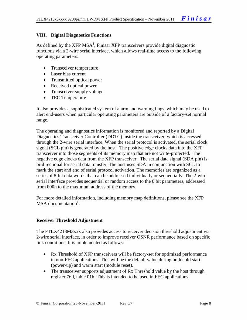
XFP Host Board Mechanical Layout (dimensions are in mm)
FTLX4213x3xxxx 3200ps/nm DWDM XFP Product Specification – November 2011 F i n i s a r
Finisar Corporation 23-November-2011 Rev C7 Page 12
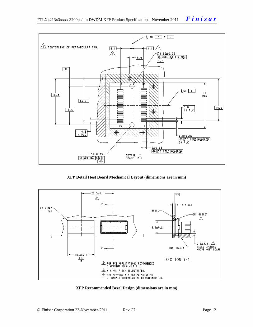
XFP Detail Host Board Mechanical Layout (dimensions are in mm)
XFP Recommended Bezel Design (dimensions are in mm)

FTLX4213x3xxxx 3200ps/nm DWDM XFP Product Specification – November 2011 F i n i s a r
Finisar Corporation 23-November-2011 Rev C7 Page 13
XI. Notes & Exceptions
The FTLX4213x3xxxx product family has the following exceptions to the XFP
MSA;
o Tx_Disable time of <100usec,
o Tx_Disable negate time of <60seconds
o Tx_NR is not implemented.
o Reset Completion Bit is not implemented in EEPROM (Table 0: Byte 84: Bit 0)
XII. References
1. 10 Gigabit Small Form Factor Pluggable Module (XFP) Multi-Source Agreement
(MSA), Rev 4.5 – August 2005. Documentation is currently available at
http://www.xfpmsa.org/
2. Application Note AN-2035: “Digital Diagnostic Monitoring Interface for XFP
Optical Transceivers” – Finisar Corporation, December 2003
3. Directive 2002/95/EC of the European Council Parliament and of the Council,
“on the restriction of the use of certain hazardous substances in electrical and
electronic equipment”. January 27, 2003.
4. “Application Note AN-2038: Finisar Implementation Of RoHS Compliant
Transceivers”, Finisar Corporation, January 21, 2005.
XIII. Revision History
Revision Date Description
A1 4/15/2008 Preliminary document created.
C1 7/20/2009 Updated Optical Spec for OSNR & Rx_Sensitivity
Updated Tx_Disable <100us
C2 3/18/2010 Updated Icc3 value
Corrected Finisar Part Numbers
C3 8/28/2010 Added “Notes & Exceptions” Section
C4 12/16/2010 Updated channel availability
C5 2/08/2011 Added additional C-band Product Codes
C6 2/24/2011 Corrected Tx_Disable max value typo in Section III
C7 11/23/2011 Updated C-band Product Codes

FTLX4213x3xxxx 3200ps/nm DWDM XFP Product Specification – November 2011 F i n i s a r
Finisar Corporation 23-November-2011 Rev C7 Page 14
XII. For More Information
Finisar Corporation
1389 Moffett Park Drive
Sunnyvale, CA 94089-1133
Tel. 1-408-548-1000
Fax 1-408-541-6138
www.finisar.com