Embed Size (px)
Citation preview

NASA-CR-198859
/L-//j//
//_,- _'_ --_...
c_CtT.
f_ _0
DIAMOND THIN FILM TEMPERATURE
AND HEATIFLUX SENSORS
M. Aslam, G. S. Yang, A. Masood and R. Fredricks
Department of Electrical Engineering
Michigan State University
East Lansing, MI
Grant NAG-l-1328
July 3, 1995
National Aeronautics and Space Administration
Langley Research Center
Hampton, Virginia 23681-0001
(NASA-CR-198859) DIAMOND THIN FILM
TEMPERATURE AND HEAT-FLUX SENSCRS
Final Report (Michigan State
Univ.) 20 p
N95-30847
Unclas
G3/76 0056854
https://ntrs.nasa.gov/search.jsp?R=19950024426 2018-06-12T05:50:34+00:00Z

Table of Contents
Section
ABSTRACT
I,
II.
III.
IV,
V.
VI.
INTRODUCTION
SENSOR INFRA-STRUCTURE
II. 1 Diamond Film Growth
II.2 Nucleation, Patterning and Doping
II.3 Metallization and Electronic Properties
II.4 Reliability
SENSOR TEST CHIPS
III. 1 1st Generation Test Chip
III. 1.1 Temperature Sensors
III.1.2 Heat Flux Sensors
III.1.3 Problems
III.2 2nd Generation Test Chip
III.2.1 Ultra-High Nucleation Density Technique
III.2.2 Thermistor Response
III.3 3rd Generation Test Chip
3-D DIRECT-WRITE PATTERNING SYSTEM
CONCLUSIONS
REFERENCES
Page
i
!
2
2
2
3
4
5
5
6
7
10
10
ll
13
14
14
15
16

Abstract
Diamond film temperature and heat-flux sensors are developed using a technology
compatible with silicon integrated circuit processing. The technology involves diamond /
nucleation, patterning, doping and metallization. Multi-sensor test chips were designed and
fabricated to study the thermistor behavior. The minimum feature size (device width) for 1st and
2rid generation chips are 160 and 5 p.m, respectively. The p-type diamond thermistors on the 1st_eneration test chip show temperature and response time ranges of 80-1270 K and 0.29-25 lus, /
i -/respectively. An array of diamond thermistors, acting as heat flux sensors, was successful y
fabricated on an oxidized Si rod with a diameter of 1 cm. Some problems were encountered in the
patterning of the Pt/Ti ohmic contacts on the rod, due mainly to the surface roughness of the
diamond film. The use of thermistors with a minimum width of 5 I.tm (to improve the spatial
resolution of measurement) resulted in lithographic problems related to surface roughness of
diamond films. We improved the mean surface roughness from 124 nm to 30 nm by using an ultra
high nucleation density of 1011 cm 2. To deposit thermistors with such small dimensions on a
curved surface, a new 3-D diamond patterning technique is currently under development. This
involves writing a diamond seed pattern directly on the curved surface by a computer-controllednozzle.
I INTRODUCTION
Commontypesof temperaturesensors[1,2,3] arethermocouples,resistancetemperaturedetectors (RTD), thermistors, integrated circuit (IC) sensors, diodes and transistors.Thermocouples[4] offer the largestrange(33 to 2573K) and linear responsebut are the leastsensitive.RTDs[5] showpoorsensitivityandlimitedrange(33 to 923K). Thethermistors[6,7,8]with a reportedrangeof 173to 1173K arevery sensitivebut nonlinear.The IC sensorsoffer ashortrange(223to 408 K), agoodlinearityandhighsensitivity.Thereportedresponsetimesforvarioustypesof temperaturesensorsare in the rangeof fraction of a secondto few hundredseconds.Thesesensorsfail or showpoor sensitivityandresponsein harshenvironmentssuchasthoseprevailing in aerospacesystems.New material technologiesare, therefore,neededfortemperaturesensorswith high sensitivity,largetemperaturerange,fast responsetime, and highrcsistanceto harshenvironments(mechanical,chemicalandradiation).
Due to a unique combination of its mechanical,electrical, thermal and chemicalproperties,diamondis an excellentmaterial for temperatureand heat flux sensors.Althoughnaturalandsyntheticdiamondthermistors[9] weredemonstratedfor temperaturesbelow600 Kalreadyin the sixties,they werenevercommercializedduemainly to high cost.Recently,therehasbeena renewedinterestin diamondthermistors[10] becauseof arapid progressin diamond
film fabrication using the chemical vapor deposition (CVD) processwhich can produceinexpensivepolycrystallinediamondfilms on non-diamondsubstratessuchas Si. In the past
severalyears,Michigan StateUniversity has providedleadershipin thedevelopmentof diamond-based sensorsand micro-machining[11,12,13](Fig. 1).Thegoalsof the researcheffort are to
develop (i) diamond sensorsfor temperature,pressureandacceleration,and(ii) diamondfield emitters for fiat paneldisplaysandpressuresensors.The research approachconsists of (a) study offundamental concepts, (b)development of materialstechnology and (c)fabricationof prototypes.
I DIAMOND
I SENSOR INFRA-STRUCTUREm
SENSORS/MICROMACHINING
+SENSOR TEST CHIP
[N CLEA ON.]
I ELECTRONIC
RELIABILITY
DIAMOND FILM-
COATINGS: abrasive.
protective, optical
+11TE ,PERA "E1
I PIEZORESISTIVE; ]pressure, acceleration
PROTOTYPES: pressure
sensors, aeeelerometers, ther-
mistors, flatpanel displays
Fig. 1 Sensor research at Michigan State University.

A 1stgenerationtest chip containingdiamondthermistors[12] with a minimum devicewidth of 160gm, developedfor NASA Langley,showedhighsensitivityin thetemperaturerangeof 80 - 1270K in vacuum.The responsetimesat 300 K were 25 las(measured)and 290 ns(calculated)for silicon and SiO2 substrates,respectively.In a further study, a 2nd generation
multi-sensortestchip wasdeveloped.Theminimumthermistorwidth on thechip is 5 gm. A new3-D patterningtechniqueis being developedto transfersuchsmall featuresizeson a curvedsurface.Thisreportdescribesthework donefor NASA Langley.In particular,(a)diamondsensorinfra-structure,(b) design,fabricationandtestingof a flat multi-sensortestchip,and(c) heatfluxsensorson flat andcurvedsubstrateswill bediscussed.
II SENSOR INFRA-STRUCTURE
To develop reproducible and reliable diamond micro-sensors and field emitters [13,14], it
was necessary to develop sensor infrastructure. The infrastructure development, compatible with
Si integrated circuit technology, includes diamond film growth, nucleation, patterning, doping,
metallization, electronic properties and reliability which are described in this section:
ILl Diamond Film Growth
High quality p-type polycrystalline diamond films were deposited on oxidized Si
substrates using hot filament CVD [15,16]. The filament and substrate temperatures were 2073 -
2473 and 1073 - 1273 K, respectively. The gases used for film growth consisted of either
hydrogen with 1% C2H 2 and 0.5% CO or hydrogen with 1% CH 4. The deposition pressure,
growth rate and film thickness were typically in the range of 50 - 70 torr, 0.15 - 0.5 p.m per hour
and 1.5 - 6 p.m, respectively. The film quality was monitored by Raman spectroscopy, scanning
electron microscopy (SEM), and atomic force microscopy (AFM).
II.2 Nucleation, Patterning and Doping
For diamond growth on non-diamond substrates, the substrate surface is treated, usually
with diamond powder, to enhance the nucleation density. The conventional diamond film
nucleation and patterning techniques require some treatment of the substrate surface which
normally causes a surface damage [17,18,19,20]. Our nucleation and patterning techniques
[21,22] do not damage the surface and are IC-compatible.
In our techniques, diamond powders with mean sizes of 0.038 or 0.101 gm are suspended
into carrier fluids to prepare the so called diamond powder loaded fluid (DPLF). As shown in
Fig.2, the DPLF is coated on an oxidized Si wafer and then patterned using standard
photolithography. The sample is subsequently placed in the diamond deposition reactor and the
carrier materials evaporate at 1163 K leaving behind the diamond powder particles whichact as
1

seedsfor diamondgrowth.The techniquescanbeusedto grow polycrystallinefilms ona varietyof substratesof different shapes,and canbe used for mechanicaland optical coatings.It is
amenableto ultrahigh nucleationdensity (above l0 II cm"2) and low temperature(-743 K)
diamondgrowth[23].
SiO2(3 gm) ISi _ [
Oxidized Si wafer.
DPLF(- 1lain)
SiO 2
Si
DPLF coating.
Diamond Film(1-3_lm)DPLF(- 11.tm) Diamond powders
SiO 2 SiO2 SiO 2
Si
Lithographic patterning.
Si
After heating to 1163 K
Si
After diamond deposition.
Fig. 2 Patterning of diamond film by DPLF method (not to scale).
The films were doped p-type during the growth process, as described in section II- l, using
pure boron powder which was placed in a holder on the substrate heater plate near the substrate so
that the holder temperature was close to 1163 K. Electronic properties of the p-type films are
described in the next section.
II.3 Metailization and Electronic Properties
Most of the earlier metallization studies [24,25,26,27] focused on ohmic contacts on
polycrystalline and single crystal diamond. As our aim was to fabricate diamond sensors, the
choice of contact metal was based on (i) ohmic contacts, (ii) good adhesion to both diamond and
silicon dioxide and (iii) resistance to high temperatures (up to 1273 K). A double-layer structure
consisting of Pt on Ti was selected. Ti makes ohmic contacts with diamond [28,29] and provides a
good adhesion between diamond and SiO 2, whereas Pt is resistant to oxidizing ambients. An
anneal for 30 min at 923 K in vacuum (10 -7 tort) resulted in stable and reproducible contacts. It is
believed that, during this anneal, Ti reacts with diamond to make its carbide [30] and it reacts with
Pt to make its alloys [31 ] which are stable at 1273 K. The quality of diamond, monitored through
SEM and Raman, was not affected by this anneal. For low temperature applications, A1 or Cr are
used as contact metals.
Hall mobility, holeconcentrationandresistivityweremeasuredfor differentdopinglevels
andat varioustemperatures.TheHall mobility andresistivityp arein therangesof 2 - 50cm2V
ls-1and0.2 - 70 f2-cm,respectively[12]. Theactivationenergiesfor boron,computedfrom theslopesof measuredp versus1/Tcurvesassumingnocompensation,arein therangeof 0.22- 0.34eV for theunannealedsamples.Thesevaluescorrespondto holeconcentrationvaluesin therangeof 1018- 2.0x 1015cm-3.
II.4 Reliability
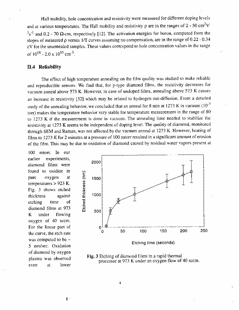
The effect of high temperature annealing on the film quality was studied to make reliable
and reproducible sensors. We find that, for p-type diamond films, the resistivity decreases for
vacuum anneal above 573 K. However, in case of undoped films, annealing above 573 K causes
an increase in resistivity [32] which may be related to hydrogen out-diffusion. From a detailed
study of the annealing behavior, we concluded that an anneal for 8 min at 1273 K in vacuum (10 -7
ton-) makes the temperature behavior very stable for temperature measurement in the range of 80
to 1273 K if the measurement is done in vacuum. The annealing time needed to stabilize the
resistivity at 1273 K seems to be independent of doping level. The quality of diamond, monitored
through SEM and Raman, was not affected by the vacuum anneal at t273 K. However, heating of
films to 1273 K for 2 minutes at a pressure of 100 mtorr resulted in a significant amount of erosion
of the film. This may be due to oxidation of diamond caused by residual water vapors present at
100 mtorr. In our
earlier experiments,
diamond films were
found to oxidize in
pure oxygen at
temperatures > 923 K.
Fig. 3 shows etched
thickness against
etching time of
diamond films at 973
K under flowing
oxygen of 40 sccm.
For the linear part of
the curve, the etch rate
was computed to be -
5 nm/sec. Oxidation
of diamond by oxygen
plasma was observed
even at lower
E¢-
v
¢/1¢._I1)t-
.o¢-
"OI1)t-o
IIi
2000
1500
1ooo
500
00 50 100 150 200 250
Etching time (seconds)
Fig. 3 Etching of diamond films in a rapid thermalprocessor at 973 K under an oxygen flow of 40 sccm.

temperatures[33].Thus,in anoxygenambient,thethermistoris stableon!ybelow923K. Theuseof thermistorinanoxidizingambientsathigh temperaturesmaybepossibleif thediamondfilm ispassivatedfor examplewith SiO2or Si3N4, which may,however,increasethe responsetimeofthethermistor.
III SENSOR TEST CHIPS
To study the electronic and sensing properties of CVD diamond, and to fabricate prototype
sensors, 1st and 2nd generation sensor test-chips were developed. The 1st generation test chip was
used solely for NASA research. The 2nd generation chip was used for NASA research as well as
for research on piezoresistive sensors [11].
The 1st generation test chip, with a chip size of I x I cm 2 and minimum diamond device
width of 160 pm, contains thermistors, Hall Van der Pauw structure and a metal-oxide-
scmiconductor field effect transistor (MOSFET). The 2nd generation test chip was used to study
the fabrication technology of very small size thermistors. This test chip, in addition to structures
found on the 1st generation chip, contains a pressure sensor, an accelerometer, a Hall sensor and
cantilever beams. It has a minimum diamond feature size (thermistor width) of 5 _tm. A six-mask
process is employed for its fabrication using four-inch Si wafers as substrates. The results
reported in this section deal with the test chips.
III.1 1st Generation Test Chip
The first generation diamond
test chip (Fig. 4) was primarily
designed for the study of thermistors.
This study led to the technology of
heat flux gauges on oxidized Si rods
with a diameter of 1 cm. The chip
uses 500 [tm thick oxidized Si wafer
as the substrate material. The
thermistors consist of p-type
polycrystalline diamond films with a
thickness in the range of 4 - 6 pm.
The metal contacts consist of Pt/Ti
double layer whereby Ti enhances
adhesion between Pt and diamond.
Fig. 4 First generation diamond test chip.

III.l.1 Temperature Sensors
The resistivity measured as a function of temperature, for the thermistors on the 1st
generation chip with three different hole concentration levels, is shown in Fig. 5(a). All the
samples were annealed at 873 K and 1273 K for 35 and 8 minutes, respectively, at a pressure of
10-7 ton before the measurements. The temperature response was measured over the temperature
range of 80 - 1273 K and(a)
found reproducible for aliP,.
number of temperature
cycles of less than 1 10'
minute duration. The
thermistors have a negative 101
temperature coefficient_= I0°
(NTC) of resistance over ..
the entire range. As _ 10-1
shown in Fig. 5(b), the A9/ _ I0 "z
O'l
AT values computed from =
the curves shown in Fig. 10.3
5(a) are in the ranges of
5.0 x 10 -7 - 7.0 x 10⁻³, 6.0 1040
x 10-6- 1 and 6.0 x 10⁻⁶- 2
f_-cm/K for the hole (b)concentrations of 9.6 x
1018, 1.72 x 10¹⁶ and 2
x 1015 cm-3, respectively.
The temperature
coeft_cient o_, defined by ot
= p-JAp/AT, is in the range
of-0.005 to -0.02 K -l for
the measured temperature
range and for the above
hole concentration values.
As the average value [3] of
c_ for Pt RTD is 0.003853
K -1, the sensitivity of
diamond sensors is better
than that of Pt RTD over
200 400 600 800 1000 1200 1400
TEM?E?,ATUR_(K)
10° I
10"1 1 • •.
10"2 f • ,• & • •
10-3 f " , • •
10"41 . . '10.s If10"_ f i • 9"6xlOn ¢m'3 • "_ "
10"71 ................ , i, _, J , ,o 200 4.oo 600 soo _ooo _2oo t4o6
TB_F._TU_ (X)
Fig. 5 The resistivity p and Ap/AT ploted as funtion of temperature
for samples with three different hole concentration.

mostof thetemperaturerange.However,mostthermistorsshowatypical valueof ct in therange
of 0.2- 0.4but overa limited temperaturerange,typically 100K [3]. Although,_ is widely usedto representthe sensitivityof temperaturesensors,it wasbasicallydevisedfor RTDs andis notsuitable for comparisonof sensitivity for semiconductorsensors.For example, a 100 Kf2thermistorand a 25 f2 RTD, both with t_ = 0.001 and temperature change of 1 K, will show
resistance changes of 100 _ and 25 mD, respectively. The change of 100 _ is readily measurable
while the change of 25 mr2 requires precision test equipment. Thus, the best measure for diamond
thermistors is Ap/AT.
The dynamic thermal response time of thermistors on the 1st generation chip, measured
by applying a square wave current pulse to the sensor, was found to be 25 Its. This is a fairly small
time constant as compared to commercial temperature sensing devices [3] with time constant in
the range of milliseconds to several tens of seconds. To achieve fast response, sensors are usually
mounted on thermal insulators such as A1203 or fused quartz [34]. As in our case the sensor is
separated from the 500 Itm thick Si substrate only by a 2 Itm thick layer of SiO 2, the response
time of 25 Its is expected to be dominated by the thermal properties of Si. The time constant can
be computed for a SiO 2 substrate using the thermal properties of Si and SiO 2. Such a computation
predicts a time constant of 0.29 Its for a diamond sensor directly on the SiO 2 substrate. This value
may be reduced further (i) by reducing the thermal mass of the sensor and/or (ii) through use of
micro-machining to fabricate a free standing sensor element.
111.1.2 Heat Flux Sensors
After an intensive study of diamond temperature sensors, arrays of diamond heat flux
sensors were fabricated on (i) a 2 x 3 cm 2 flat oxidized Si wafer and (ii) an oxidized Si rod with a
length of 7.6 cm and a diameter of 1 cm. The flat sample (sensor test chip) was used to study the
uniformity of doping level and difference in temperature response of individual thermistors. This
sample was sent to NASA after initial testing at Michigan State. The cylindrical substrate is
considered for possible measurement of heat flux in wind tunnels.
The flat sensor test chip consists of an array of ten thermistors with dimensions of 250 x
800 gm 2 with center to center spacing of 400 Itm. A schematic diagram of thermistor array is
shown in Fig. 6 and measurement data is listed in Table 1. The non-uniformity in film thickness
was within 4%. A variation of 7% in the width of thermistors was introduced due to the use of
transparency type masks. The resistivity was measured as a function of temperature in the range
of 300 - 673 K for selected thermistors. The temperature response for each thermistor was stable
and repeatable after an anneal for 10 min at 673 K. Fig. 7(a) shows the resistivity as a function of
temperature for selected diamond thermistors. A large variation in the initial resistivity values for
thermistors fabricated at the same run was observed. It is believed to be due to the nonuniform
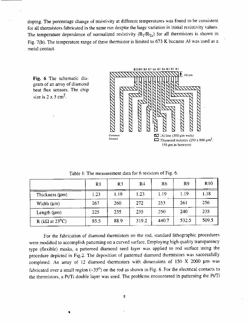
doping.The percentagechangeof resistivityatdifferent temperatureswasfoundto beconsistentfor all thermistorsfabricatedin thesamerundespitethe largevariationin initial resistivity values.The temperaturedependenceof normalizedresistivity (RT/RTo)for all thermistorsis shownin
Fig. 7(b).Thetemperaturerangeof thesethermistoris limited to 673K becauseA1wasusedasametalcontact.
Fig. 6 The schematicdia-gramof anarrayof diamondheat flux sensors.The chipsizeis 2 x 3 cm2.
4
\
\
\
N
\
\
\
\
\
\
\
"xN.
N,
\
Common
Ground
R10R9 R8 R7 R6 R5 R4 R3 R2 R1
N
NNN\\\N_I 35o.m
I'k"l :AI line (300 _tm wide)
I"1 "Diamond resisters (250 x 800 t.lm 2,
150 lam in between)
Table 1: The measurement data for 6 resistors of Fig. 6.
R 1 R3 R4 R6 R9 R 10
Thickness (gm) 1.23 1.19 1.23 1.19 1.19 1.18
Width (gm) 267 260 272 253 261 256
Length (gm)
R (kf2 at 23°C)
225
85.5
235
88.9
235
319.2
25O
440.7
240
532.5
235
509.5
For the fabrication of diamond thermistors on the rod, standard lithographic procedures
were modified to accomplish patterning on a curved surface. Employing high quality transparency
type (flexible) masks, a patterned diamond seed layer was applied to rod surface using the
procedure depicted in Fig.2. The deposition of patterned diamond thermistors was successfully
completed. An array of 12 diamond thermistors with dimensions of 150 X 2000 lam was
fabricated over a small region (~35 °) on the rod as shown in Fig. 8. For the electrical contacts to
the thermistors, a Pt/Ti double layer was used. The problems encountered in patterning the Pt/Ti

contactsweremainlyrelatedtheetchingof PtfFi.
(a) 80
E?
>.m
(o
CD
60
40
20
0
@ou
o
0
% %V
qlv%
o[]
v%_V o
AI iN
D
0
Jam A •
zx R1
• R3
• R4
v R6
[] R9
o R10
÷°_o_, _o _i__A U ,', A •___IIAj
300 400 500 600
(b) 1.00
rr
n" 0.75
>
ffl0.50
N
t_
E 0.25O
z
0
Temperature (K)
Equation: l/x=a+b(In(y))+c(In(y))2+d(In(y)) 3, K"_'
96.837 K"1, b=-I 10.979 K"1, c=-3.10559 K1 , d=-3.70552Data fitting
zx R1
li_ • R3_, • R4
-'_ v R6'_ [] R9 '
300 400 500 600
Temperature (K)
Fig. 7 The resistivity (a) and normalized resistivity (b) versus temperature
for selected diamond thermistors. (T o = 300 K)

(a) __:_,_-_i:-_-- III.1.3 Problems
(b)
(c)
The technology developed for
the 1st generation diamond test chip
demonstrated successfully the
excellent sensing properties of
diamond thermistors. However, this
also revealed some problems related
to small feature sizes, 3-D patterning
and metal contacts. The surface
roughness of diamond films used in
the first generation test chip was in
the range of 0.5 -2 l.tm depending
upon the film thickness. This results
mainly from polycrystalline nature of
the films and the low diamond
nucleation density which is in the
range of 10 8 cm -3. Due to the
roughness; (i) the targeted
dimensions of small feature sizes
were difficult to achieve, (ii)
problems were encountered in post-
deposition lithography, and (iii) the
etching of metal contacts was
complicated. To study such
problems, a 2nd generation test chip
was designed, fabricated and tested.
A new 3-D patterning techniques was
developed to overcome the problems
associated with diamond film
patterning on curved surfaces.
III.2 2nd Generation Test ChipFig. 8 Pictures of diamond thermistors on the
Si rod (a-c). A second generation test chip,
with a minimum feature size of 5 l.tm, was developed. It has a variety of test structures including
thermistors, a pressure sensor, an accelerometer, a magnetic field sensor and a metal-oxide-
semiconductor field effect transistor (MOSFET). Fig. 9 shows an overview of this chip. The chip
was used to study the surface roughness and thermistor response.
10
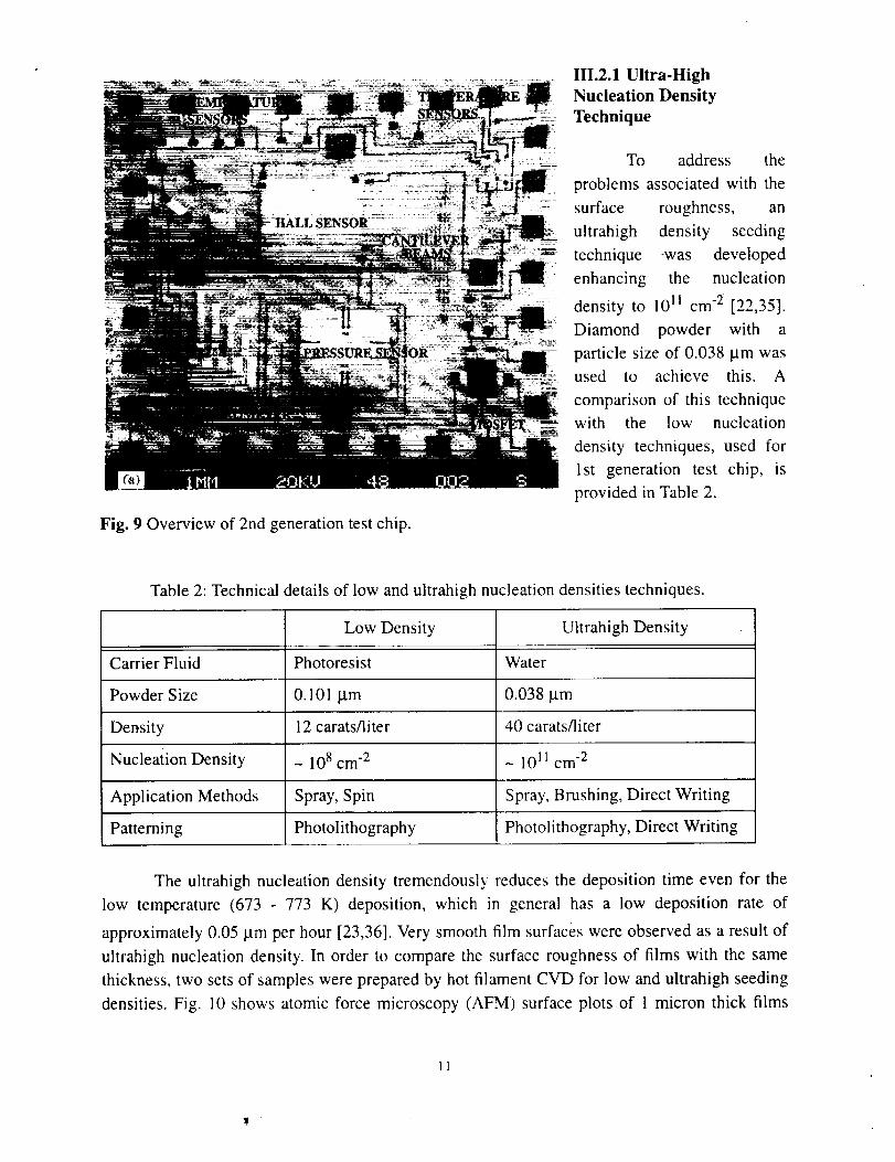
Fig. 9 Overviewof 2ndgenerationtestchip.
III.2.1 Ultra-High
Nucleation Density
Technique
To address the
problems associated with the
surface roughness, an
ultrahigh density seeding
.... technique -was developed
enhancing the nucleation
density to 1011 cm -2 [22,35].
Diamond powder with a
particle size of 0.038 gm was
used to achieve this. A
comparison of this technique
with the low nucleation
density techniques, used for
1st generation test chip, is
provided in Table 2.
Table 2: Technical details of low and ultrahigh nucleation densities techniques.
Low Density Ultrahigh Density
Carrier Fluid Photoresist Water
Powder Size 0.101 gm 0.038 gm
Density 12 carats/liter 40 carats/liter
Nucleation Density _ 108 cm-2 _ 1011 cm -2
Application Methods Spray, Spin Spray, Brushing, Direct Writing
Patterning Photolithography Photolithography, Direct Writing
The ultrahigh nucleation density tremendously reduces the deposition time even for the
low temperature (673 - 773 K) deposition, which in general has a low deposition rate of
approximately 0.05 gm per hour [23,36]. Very smooth film surfaces were observed as a result of
ultrahigh nucleation density. In order to compare the surface roughness of films with the same
thickness, two sets of samples were prepared by hot filament CVD for low and ultrahigh seeding
densities. Fig. l0 shows atomic force microscopy (AFM) surface plots of 1 micron thick films
11
1 "

seeded by nucleation densities of-10 8 cm-2 and -10 11 cm - 2.The average surface roughness for
(a) (b)
X 1.000 vM/div X |.000 _N/diuZ 500,000 nM/diu _ 500.000 nN/div
r(c)
X 0.200 jm/diu2 250,000 nN/div X 0.200 _w/div
2 250.000 nu/div
Fig. 10 Atomic force microscopy micrographs of 1 ktm thickness films for low (a, c)
and ultrahigh (b, d) nucleation densities.
Fig. 11 Pictures of thermistors (a) used for temperature response,
and close-up view of 5 pm wide thermistor (b).
12

the ultrahigh density is approximately 30 nm as compared to 124 nm for the low density [35].
111.2.2 Thermistor Response
The resistors used for the temperature sensing properties are shown in Fig. 11 which also shows a
close-up view of the thermistor with a feature size of 5 I.tm in width. The thermistor response is
shown in Fig. 12 and the film properties are summarized in Table 3.
(a) 100
E 10¢.)
.>_
(/)
In-
0.1200
I [] Low density test chip I[] O High density test chip[]
El3
400 600 800 1000
(b) 100
Temperature (K)
E 10O
d
rr
0.1
IO Low density test chip I[] High density test chip I
0.0010 0.0015 0.0020 0.0025 0.0030 0.0035
1/T (K"_)
Fig. 12 The temperature response of resistivity for both high and low nucleation density samples.
13

The Hall mobility and concentration are measured by Hall Van der Pauw method [37]. The
temperature response of resistivity for both low and ultrahigh nucleation densities samples was
measured in the temperature range of 300 - 825 K. As seen in Fig. 12 (b), the two straight lines
with different slopes intersected at a temperature of 525 K for the ultrahigh density sample. It
suggests two activation energies for boron in highly doped diamond within this temperature
range. The high density sample has a lower resistivity and higher Hall concentration than low
density one. The larger amount of grain boundaries, which contain more dopant impurities and
defects, present in high nucleation density samples is believed to contribute to the higher
conduction of high-density samples.
Table 3: The characteristic of films seeded by low and ultrahigh densities.
Low Density Ultrahigh Density
Nucleation Density (cm -2) ~ 108 - 1011
Average Surface Roughness (nm) 124 30
Maximum Roughness (nm) 888 264
Resistivity (f2-cm) 27.0538 6.9461
Hall Mobility (cm2/V-s) 0.9141 1.0938
Hall Concentration (cm -3) 2.5273 x 10¹⁷ 8.226 x 10¹⁷
III.3 3rd Generation Test Chip
The design of 3rd generation test chip focuses on (i) small feature sizes (1-2 gm), (ii) free
standing thermistor structures to enhance response time and (iii) mass air flow sensors. The small
feature size will permit high resolution of temperature variations. For the operation of diamond
thermistors in oxidizing environments, a passivation layer (SiO 2 or Si3N4) is required to prevent
diamond from oxidation at a temperature higher than 873 K. However, the passivation layer may
increase the response time. In order to improve the sensor's response time, a free standing
structure is useful to minimize the amount of heat dispensed into the substrate. These and other
issues are currently addressed in the design of third generation test chip.
IV 3-D DIRECT-WRITE PATTERNING SYSTEM
In spite of its many advantages, the patterning technique currently employed in our sensor
fabrication processes is limited to flat substrates. Additionally, as shown in Fig. 11 (a) and (b), the
stray diamond panicles with a density of-105 cm -2 appear in non-diamond areas. They cause a
serious problem if thick diamond films are grown. A new patterning technique for CVD diamond
14

is currently under development to achieve both arbitrary shaped and highly selective diamond
patterning. In this technique, diamond seed patterns are directly written on a substrate [38] using
fine nozzles. A schematic diagram is shown in Fig. 13. Computer controlled 3-dimensional
position stages coupled with nozzles are used to write patterns on a substrate. Such a direct-write
system is currently under construction. The system is expected to help produce heat flux sensors
on curved substrates.
Fig. 13 Schematic diagram of direct-
write diamond seeding system.
Bell jar chamber
Computer__
I
Flow ]controller
_lJ.....Pump
V CONCLUDSIONS
Boron-doped CVD diamond thermistors show temperature and response time ranges of 80
- 1270 K and 0.29 - 25 Its, respectively. The use of thermistors with a minimum feature size of 5
Itm (to improve the spatial resolution of measurement) resulted in lithographic problems related
to surface roughness of diamond films. We improved the surface roughness to 30 nm by using an
ultrahigh nucleation density of 1011 cm -2. To transfer such small thermistors on a curved surface,
a new 3-D diamond patterning technique is currently under development. This involves writing a
diamond seed pattern directly on the curved surface by a computer-controlled nozzle.
15

REFERENCES
1. W. Schafer, Sensors and Actuators, 17, 27-37 (1989).
2 S. Middelhoek and S. A. Audit, Silicon Sensors, Academic Press, London (1989).
3 T.D. McGee, Principles and Methods of Temperature Measurements, John Wiley & Sons
(1988).
4 A. Boyer, E. Cisse, Y. Azzouz and J. P. Cheron, Sensors and Actuators, A, .25-27, 637-640
(1991).
5. D.E. Bahniuk, Machine Design, 111-114, Feb, (1989); W. J. Tompkins and J. G. Webster,
Interfacing Sensors to the IBM PC, Prentice Hall, Englewood Cliffs, NJ (1988).
6. T. Nugai and M. Itoh, IEEE Trans. Industry Applications, 26(6), 1139-1143 (1990).
7. C.E. Woodhouse, IEEE Trans. Instrum. and Meas., 39(1), 279-284 (1990).
8. S.A. Obukhov, B. S. Neganov, Y. E Kiselov, A. N. Chernikov, V. S. Vekshina and N. I. Pep-
kik and A. N. Popkov, Cryogenics (UK), 31(10), 874-877 (1991).
9. G.B. Rogers and E A. Raal, Rev. Sci. Inst, 31,663-664 ( 1960); U.S. Patent, 3,435,399, 25
March (1969).
10. N. Fujimori and H. Nakahata, New Diamonds, 98-101 (1990).
11. I. Taher, M. Aslam, M. A. Tamor, T. J. Potter, and R. E. Elder, Sensors and Actuators:
A., Vol. 45, 35 (1994).
12. M. Aslam, G. S. Yang, and A. Masood, Sensors and Actuators: A., Vol. 45, No. 2, 131
(1994).
13. M. Aslam and D. Schulz, Proc. Int. Conf. Solid State Sensors & Actuators (Transducers 95),
Stockhom, Sweden, 1995.
14. M.W. Geis, N. N. Efremow, J. D. Woodhouse, M. D. Aleese, M. Marchywka, D. G. Socker,
and J. E Hochedez, IEEE Elec. Dev. Lett., 12, 456 (1991).
15. S. Matsumoto, Y. Sato, M. Kamo and N. Setaka, Jpn. J. Appl. Phys., 21, L183 (1982).
16. J.C. Angus and C.C. Hayman, Science, vol. 241, p. 913, (1988).
17. K. Hirabayashi and Y. Taniguchi, Appl. Phys. Lett., 53, 19 (1988); J. S. Ma, H. Kawarada,
T. Yonehara, J. Suzuki, J. Wei, Y. Yokota, and A. Hiraki, Appl. Phys. Lett., 55, 1071 (1989).
18. A.R. Kirkpatric, B. W. Ward, and N. P. Economou, J. Vac. Sci. Technol., 7, 60 (1989).
19. J.L. Davison, C. Ellis and R. Ramesham, J. Electron. Mater., 18, 711-715 (1985).
20. S.A. Grot, C. W. Hatfield, G. S. Gildenblat, A. R. Badzian, and T. Badzian, IEEE Electron.
Dev. Lett. (1991 ).
21. A. Masood, M. Aslam, M.A. Tamor, T.J Potter, J. Electrochem. Soc., 138, L67(1991).

Q
22. G.S. Yang andM. Aslam, Appl. Phys.Lett. 66(3), (1995).
23. G.S. Yang,M(Aslam, M. J.Ulczynski,andD. K. Reinhard,Proc. of 4th ICNDST, Kobe,Japan(1994).
24. H. Shiomi,H. Nakahata,T. Imai,Y.NishibayashiandN. Fujimori, Jpn.J.Appl. Phys.,28(5),758-762(1989).
25. M.W. Geis,IEEEProceedings,79(5),669-675(1991).
26. E Fang,C. A. Hewett,M. G.FernandesandS.S.Lau, IEEETrans.ElectronDevices,36,1783-1786(1989).
27. A.T. Collins,E.C. Lightowlers,andA. W. S.Williams, DiamondRes.,pp. 19-22,(Suppl.Ind. DiamondRev.)(1970).
28. G.S. Gildenblat,S.A. Grot,C. W.Hatfield,andA. R.Badzian,IEEEElectron.Dev.Lett.,EDL-12 (2),37 - 39(1991).;G.S.Gildenblat,IEEEElectron.Dev.Lett.,EDL-I 1,371-372,Sep.(1990);H. Shiomi,Y.N. Yashi,andN. Fujimori, Jpn.J.Appl. Phys.,28,L2153-2154(1989).
29. J.E Prins,Appl.Phys.Lett.,41(10),950-952(1982).
30. J.E. Field, ThePropertiesof Diamond,AcademicPress,(1971).
31. S.A. Grot,G. S.Gildenblat,C.W.Hatfield,C. R. Wronski,A. R. Badzian,T.BadzianandR. Messier,IEEEElectronDev.Lett.,EDL-11(2), 100-102(1990).
32. M.I. LandstrassandK. V.Ravi,Appl. Phys.Lett., 55 (14), 1391- 1393(1989);L. S.Pan,D. R. Kania,S.Han,J.W. Ager III, M. Landstrass,O.L. LandenandE Pianetta,Science,255,830-833(1992).
33. H. ChiemiandY. Sato,NewDiamond,6, 32 (1990).
34. R.J. Vidal, ComellAeronauticalLaboratoryBuffalo NY rept.,AD-917-A-1(1956).
35. G.S. Yang,M. Asalm,K. E Kuo, D. K. Reinhard,andJ.Asmussem,J.Vac.Sci.andTech-nol.,May/June,(1995).
36. H.W. Ko, S.E.Hsu,S.J.Yang,M. S.Tsai,and2: H. Lee,DiamondandRelatedMaterials,2, 694(1993).
37. L.J. VanderPauw,PhillipsRes.Repts.,13,1-9(1958).
38. M. Aslam,PendingPatent,MichiganStateUniversity, 1994.