Embed Size (px)
Citation preview
Exploring and Analyzing the Real Impact of ModernOn-Package Memory on HPC Scientific Kernels
Ang LiPacific Northwest National Lab, USA
Weifeng Liu1,2
1. University of Copenhagen,Denmark
2. Norwegian University of Scienceand Technology, Norway
Mads R.B. KristensenUniversity of Copenhagen, Denmark
Brian VinterUniversity of Copenhagen, Denmark
Hao WangVirginia Tech, [email protected]
Kaixi HouVirginia Tech, USA
Andres MarquezPacific Northwest National Lab, USA
Shuaiwen Leon Song1,2
1.Pacific Northwest National Lab2. College of William and Mary, USA
ABSTRACTHigh-bandwidth On-Package Memory (OPM) innovates the conven-
tional memory hierarchy by augmenting a new on-package layer
between classic on-chip cache and off-chip DRAM. Due to its rela-
tive location and capacity, OPM is often used as a new type of LLC.
Despite the adaptation in modern processors, the performance and
power impact of OPM on HPC applications, especially scientific
kernels, is still unknown. In this paper, we fill this gap by conducting
a comprehensive evaluation for a wide spectrum of scientific kernels
with a large amount of representative inputs, including dense, sparseand medium, on two Intel OPMs: eDRAM on multicore Broadwell
and MCDRAM on manycore Knights Landing. Guided by our gen-
eral optimization models, we demonstrate OPM’s effectiveness for
easing programmers’ tuning efforts to reach ideal throughput for
both compute-bound and memory-bound applications.
CCS CONCEPTS•Hardware → Memory and dense storage; Power estimation andoptimization; •Computer systems organization → Multicore ar-chitectures; •Computing methodologies → Model developmentand analysis;ACM Reference format:Ang Li, Weifeng Liu1,2, Mads R.B. Kristensen, Brian Vinter, Hao Wang,
Kaixi Hou, Andres Marquez, and Shuaiwen Leon Song1,2. 2017. Exploring
and Analyzing the Real Impact of Modern On-Package Memory on HPC
Scientific Kernels . In Proceedings of SC17, Denver, CO, USA, November12–17, 2017, 14 pages.
ACM acknowledges that this contribution was authored or co-authored by an employee,or contractor of the national government. As such, the Government retains a nonexclu-sive, royalty-free right to publish or reproduce this article, or to allow others to do so,for Government purposes only. Permission to make digital or hard copies for personalor classroom use is granted. Copies must bear this notice and the full citation on thefirst page. Copyrights for components of this work owned by others than ACM mustbe honored. To copy otherwise, distribute, republish, or post, requires prior specificpermission and/or a fee. Request permissions from [email protected].
SC17, Denver, CO, USA© 2017 ACM. 978-1-4503-5114-0/17/11. . . $15.00DOI: 10.1145/3126908.3126931
DOI: 10.1145/3126908.3126931
1 INTRODUCTIONIn the past four decades, perhaps no other topics in the HPC domain
have drawn more attention than reducing the overheads of data move-
ment between compute units and memory hierarchy. Right from
the very first discussion about exploiting “small buffer memories”
for data locality in the 1970’s [40], caches have evolved to become
the key factor in determining the execution performance and power
efficiency of an application on modern processors.
Although today’s memory hierarchy design is already deep and
complex, the bandwidth mismatch between on-chip and off-chip
memory, known as the off-chip “memory-wall”, is still a big obstacle
for high performance delivery on modern systems. This is especially
the case when GPU modules or other manycore accelerators are
integrated on chip. As a result, high-bandwidth memory (HBM)
becomes increasingly popular. Recently, as a good representative of
HBM, on-package memory (OPM) has been adopted and promoted
by major HPC vendors in many commercial CPU products, such
as IBM Power-7 and Power-8 [14], Intel Haswell [16], Broadwell,
Skylake [28] and Knights Landing (KNL) [42]. For instance, five
of the top ten supercomputers in the newest Top 500 list [1] have
equipped OPM (primarily on Intel Knights Landing).
On-package Memory, as its name has implied, is a memory stor-
age manufactured in a separate chip but encapsulated onto the same
package where the main processor locates. OPM has several unique
characteristics: (i) they are located between on-chip cache and off-
package DRAM, (ii) their capacity is larger than on-chip scratchpad
memory or cache but often smaller than off-package DRAM; (iii)
their bandwidth is smaller than on-chip storage but significantly
larger than off-package DRAM; (iv) their access latency is smaller
or similar to off-package DRAM. Although these properties portray
OPM similar to last-level cache (LLC), their actual impact on per-
formance and power for real HPC applications, especially critical
scientific kernels, remains unknown.
SC17, November 12–17, 2017, Denver, CO, USA A. Li et al.
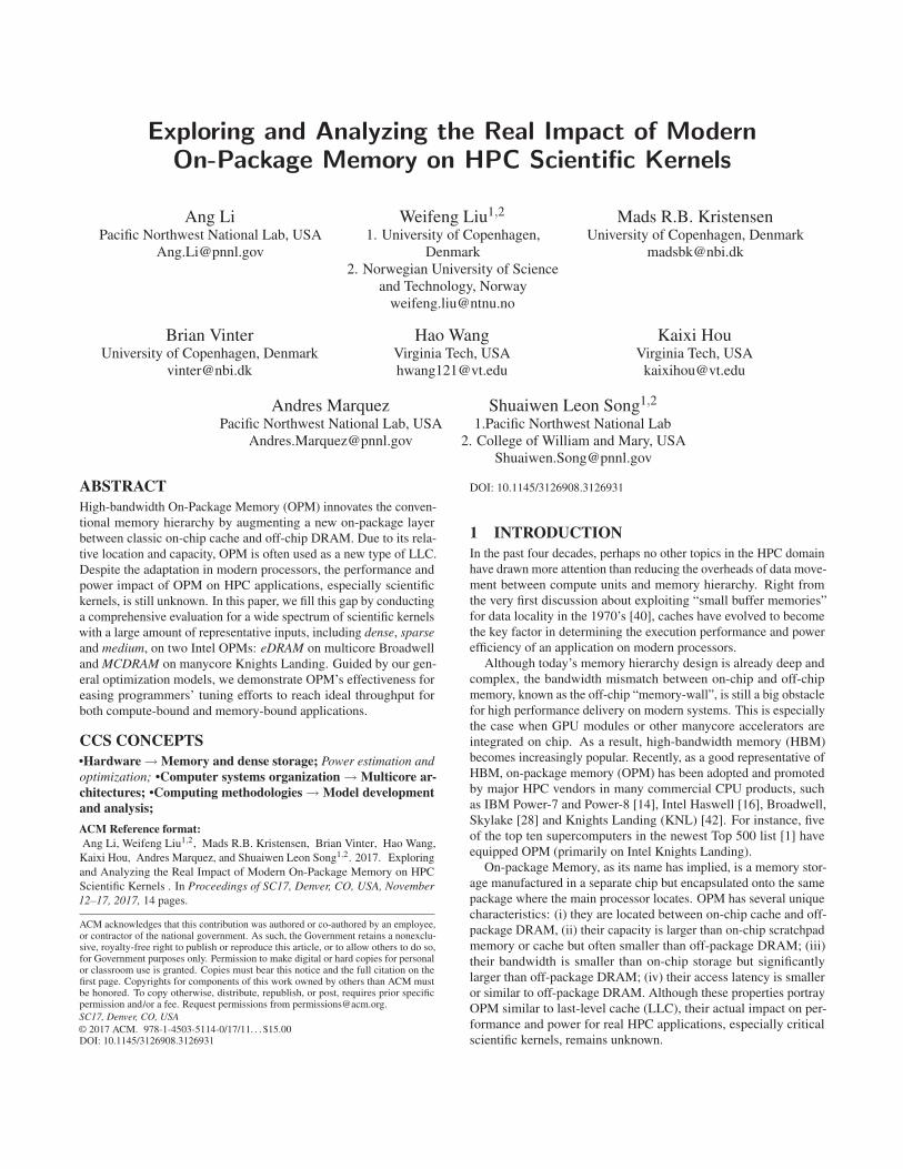
Figure 1: Probability density for achievable GEMM performance (GFlop/s) using 1024samples with different tiling size and problem size. With eDRAM, the function curve asa whole shifts more to the upper-right, implying that more samples can reach near-peak(e.g., 90%) performance. In other words, having eDRAM increases the chance for users’less-optimized applications to reach the “vendor-claimed” performance. However, theright boundary only moves a bit, indicating that eDRAM cannot significantly improvethe raw peak performance.
Exploring and analyzing such impact of modern OPM on HPC
scientific kernels is essential for both application developers and
HPC architects. Figure 1 shows an example. For a HPC system,
there is often a huge implicit gap between “claimed” attainable per-
formance and real “deliverable” performance, even with the same
algorithm. This is because the specific implementation used for
benchmarking or ranking is usually carefully hand-tuned for param-
eterization. Such an expert version is significantly different from
the one commonly used by an application developer or a HPC user.
With regard to OPM, although conventional wisdom may question
its usefulness for computation-bound applications such as GEMM,
Figure 1 uses eDRAM as an example to show that it can greatly
improve the chance for a less-optimized code to harvest near-peakperformance, dramatically mitigating the aforementioned perfor-
mance gap. In addition, recent released OPM such as MCDRAM
on Intel KNL has many architectural tuning options available so it
is important to understand how these features affect applications’
performance and energy profile. With these in mind, we conduct
a thorough evaluation to quantitatively assess the effectiveness of
two types of widely-adopted OPM. To the best of our knowledge,
this is the first work on quantitatively evaluating modern OPM on
real hardware for essential HPC application kernels while develop-
ing evaluation methodology to assist analysis on complex results to
provide useful insights.
Such evaluation is not only necessary but also fundamental for
enabling reliable technical advancement, e.g., motivating software-
architecture co-design exploration and assisting validation of mod-
eling/simulation. Particularly, this study benefits three types of
audience: (A) procurement specialists considering purchasing OPM-
equipped processors for the applications of interest; (B) application
developers who intend to estimate the potential gain through OPM
and customize optimizations; and (C) HPC researchers and archi-
tects who want to design efficient system software and architectures.
Complex scenarios observed from our evaluation can extend the
current design knowledge which can then help pave the road for new
research directions.
Contributions. In summary, this work makes the following three-
fold contributions.
• We experimentally characterize and analyze the performance
impact from two modern Intel OPM (i.e., eDRAM on Intel Broad-
well architecture and MCDRAM on Intel Knights Landing) on
several major HPC scientific kernels that covers a wide design
space. We also evaluate a very large set of their representative
input matrices (e.g., 968 matrices for sparse kernels).
• We demonstrate the observations and quantitatively analyze each
kernel’s performance insights on these two OPM. We also derive
an intuitive visual analytical model to better explain complex
scenarios and provide architectural design suggestions.
• We provide a general optimization guideline on how to tune
applications and architectures for superior performance/energy
efficiency on platforms equipped with these two types of OPM.
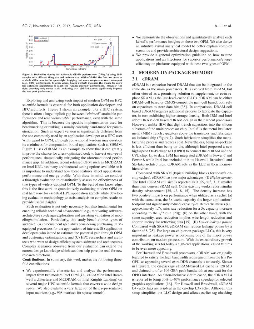
2 MODERN ON-PACKAGE MEMORY2.1 eDRAMeDRAM is a capacitor-based DRAM that can be integrated on the
same die as the main processors. It is evolved from DRAM, but
often viewed as a promising solution to supplement, or even re-
place SRAM as the last-level-cache (LLC). eDRAM can be either
DRAM-cell based or CMOS-compatible gain-cell based; both rely
on capacitors to store data bits [38]. In comparison, DRAM-cell
based eDRAM requires additional process to fabricate the capaci-
tor, in turn exhibiting higher storage density. Both IBM and Intel
adopt DRAM-cell based eDRAM design in their recent processors.
However, unlike IBM that digs trench capacitors into the silicon
substrate of the main processor chip, Intel fills the metal-insulator-
metal (MIM) trench capacitors above the transistors, and fabricates
an isolated chip (Figure 2). Such fabrication simplifies the manu-
facturing process and reduces cost. Nevertheless, being on-package
is less efficient than being on-die, although Intel proposed a new
high-speed On-Package I/O (OPIO) to connect the eDRAM and the
CPU chip. Up to date, IBM has integrated eDRAM in Power-7 and
Power-8 while Intel has included it in its Haswell, Broadwell and
Skylake architectures. eDRAM acts as the LLC in their memory
hierarchies.
Compared with SRAM (typical building blocks for today’s on-
chip caches), eDRAM has two major advantages: (I) Higher density.
The Intel eDRAM cell size is reported as 0.029μm2, 3.1x smaller
than their densest SRAM cell. Other existing works report similar
density advancement [35, 43, 8, 15]. The density increase has
two positive impacts on performance when utilized as a cache: (a)
with the same area, the 3x cache capacity fits larger applications’
footprint and significantly reduces capacity-related cache misses (i.e.,
approximately 1.7x miss rate reduction for a 3x capacity increase
according to the√
2 rule [20]); (b) on the other hand, with the
same capacity, area reduction implies wire-length reduction and
shorter latency for retrieving data [15]. (II) Lower leakage power.
Compared with SRAM, eDRAM can reduce leakage power by a
factor of 8 [25]. For large on-chip or on-package LLCs, this is very
important as leakage power is becoming one of the major power
contributors on modern processors. With the extraordinary growth
of the working sets for today’s high-end applications, eDRAM turns
to be even more appealing.
For Haswell and Broadwell processors, eDRAM was originally
featured to satisfy the high bandwidth requirement from the Iris Pro
GPU, as appending several extra DDR channels is too costly. Shown
in Figure 2, the on-package eDRAM-based L4 cache is 128 MB
and claimed to offer 104 GB/s peak bandwidth at one watt for the
OPIO interface. As a non-inclusive victim cache, the eDRAM L4
is reported to bring 30% to 40% performance speedup for selected
graphics applications [16]. For Haswell and Broadwell, eDRAM
L4 cache tags are resident in the on-chip L3 cache. Although this
setup simplifies the LLC design and allows earlier tag-checking
The Real Impact of Modern On-Package Memory on HPC Scientific Kernels SC17, November 12–17, 2017, Denver, CO, USA
Figure 2: Intel Haswell and Broadwell Processor Architecture with eDRAM
Figure 3: Intel Xeon-Phi Knights Landing Architecture with MCDRAM
for fetches from the processor, it makes the accessing to eDRAM
LLC from other devices (e.g., independent GPUs via PCIe) slower
as these memory requests have to be forwarded to on-chip L3 first
before being handled by the LLC. To address this, eDRAM has been
moved to the position upon DRAM controllers in Skylake (more
like a memory-side buffer rather than a cache).
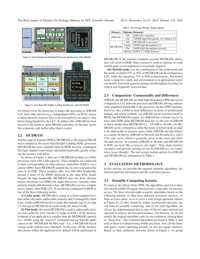
2.2 MCDRAMAnother type of popular OPM is MCDRAM, a 3D-stacked DRAM
that is adopted in the recent Intel Knights Landing (KNL) processor.
MCDRAM has more channels than its DDR memory counterpart.
The high channel count brings substantial bandwidth, greatly reduc-
ing the memory wall effect.
As shown in Figure 3, there are 8 MCDRAM modules in a KNL
processor, each with 2 GB capacity. These modules are connected
to their corresponding on-chip memory controllers (EDCs) via a
similar OPIO. Each MCDRAM module has its own read and write
ports to its EDC. The 8 modules offer over 400 GB/s bandwidth,
around 5 times of the DDR4 deployed in the same KNL board.
Despite the high bandwidth, MCDRAM does not show obvious
latency advantage over DDR with single data access. Actually, when
memory bandwidth demand is low, MCDRAM even has a higher
access latency than DDR [27]. It can also be configured in BIOS to
one of the three following modes:
(i) Cache mode: MCDRAM is acting as a direct-mapped LLC
that caches the entire addressable memory and is managed by hard-
ware. Unlike eDRAM-based L4 cache that uploads tags to on-chip
L3, the tags of MCDRAM in cache mode are stored locally.
(ii) Flat mode: the entire MCDRAM is used as addressable mem-
ory and cached by LLC (on-die L2 cache on KNL). If the memory
footprint of an application is smaller than the MCDRAM capacity
(i.e., 16GB), using the “numactl” command tool can bind the appli-
cation to the ‘MCDRAM NUMA node’ (i.e., a MCDRAM-based
storage node without cores attached). In this case, all the memory
allocations within the application by default will be performed in
Table 1: On-Package Memory Tuning Options
Memory Options Remarks
eDRAMOff eDRAM is disabled
On 128MB high-throughput, low-latency L4
MCDRAM
Off MCDRAM is not used
Cache 16GB high-throughput L3
Flat 16GB high-throughput memory
Hybrid 8GB L3 + 8GB memory
MCDRAM. If the memory footprint exceeds MCDRAM, alloca-
tion will occur in DDR. Since numactl is used at runtime, no code
modification or recompilation is essentially required.
(iii) Hybrid mode: it is the combination of the cache mode and
flat mode, in which 25% or 50% of MCDRAM can be configured as
LLC, while the remaining 75% or 50% as flat memory. The hybrid
mode is ideal for a multi-user environment or in applications which
can benefit from both general caching and throughput boosting for
critical and frequently accessed data.
2.3 Comparison: Commonality and DifferenceseDRAM and MCDRAM are both high-throughput OPM and can be
configured as LLC between processor and DRAM, offering substan-
tially amplified bandwidth to the processor via the OPIO interface.
However, they exhibit several differences in terms of architectural
features and tuning methods: (a) eDRAM can be switched on/off in
BIOS, but MCDRAM cannot; (b) eDRAM has a shorter access la-
tency than DDR while MCDRAM does not; (c) the size of eDRAM
is much smaller than MCDRAM (i.e., 128 MB vs.16 GB); (d) MC-
DRAM can be configured as either flat mode or hybrid mode in order
to be addressable in memory space, while eDRAM can only behave
as a cache. In theory, eDRAM in Haswell and Broadwell is still a
CPU-side cache, which is generally closer to the cores and offers
fast data access. In contrast, eDRAM in Skylake and MCDRAM
in KNL are more like a memory-side buffer. They show memory
semantics and provide caching service for DRAM (i.e., no consis-
tency issues though). The real-system tuning options for eDRAM
and MCDRAM are summarized in Table 1.
3 EVALUATION METHODOLOGYIn this section, we describe the targeted scientific algorithms, the
detailed platform information and the evaluation process.
3.1 Scientific Computing KernelsTo analyze the effects from OPM, the algorithms used for evalua-
tion should exhibit divergent characteristics, especially for memory
access. We have selected eight scientific algorithms based on the
following criteria: (1) they have different arithmetic intensity, or
flops-to-bytes ratios, so as to cover a wide design spectrum (shown
in Figure 4); (2) they should be widely used kernels that play cru-
cial roles in scientific computing; and (3) for each algorithm, we
choose the implementation that is state-of-the-art, open-sourced and
reported to achieve the best performance. For fairness, we do not
modify the original algorithm codes in our evaluation, treating them
as “black-box”. The evaluated algorithms are listed in Table 2, and
each of them is evaluated using double-precision. Also, all the dense
and sparse matrix-operating kernels we use are square matrices.
Based on their arithmetic intensity shown in Figure 4, we group
SC17, November 12–17, 2017, Denver, CO, USA A. Li et al.
Table 2: Scientific Kernels Characteristics. All the kernels use double-precision (DP). Thds are the optimal thread number running on Broadwell and KNL.
Algorithm Implementation Dwarf Class Type Complexity Operations Bytes Arithmetic Intensity ThreadsGEMM Plasma[4] Dense Linear Algebra Dense O(n3) 2n3 32n2 n/16 4/64
Cholesky Plasma[5, 4] Dense Linear Algebra Dense O(n3) n3/3 8n2 n/24 4/64SpMV CSR5[33] Sparse Linear Algebra Sparse O(nnz) nnz+2M 12nnz+20M (nnz+2M)/(12nnz+20M) 8/256
SpTRANS Scan/MergeTrans[44] Sparse Linear Algebra Sparse O(nnz lognnz) nnz lognnz 24nnz+8M (nnz lognnz)/(24nnz+8M) 4/64SpTRSV P2P-SpTRSV[39] Sparse Linear Algebra Sparse O(nnz) nnz+2M 12nnz+20M (nnz+2M)/(12nnz+20M) 8/256
FFT FFTW[17] Spectral Methods Others O(n logn) 5n logn 48n 5logn/48 8/256
Stencil YASK[49] Structured Grid Others O(n2) 61n2 8n2 7.625 8/256Stream Stream[36] N/A Others O(1) 2n 32n 0.0625 8/256
Table 3: Platform Configuration. “SP Perf.” and “DP Pref.” are the theoretical maximum single- and double-precision floating-point operation throughput, respectively. “C/” standsfor memory capacity. “B/” stands for memory bandwidth. “OPM” is the on-package memory. “Cache” refers to the upper-level cache respect to OPM in the memory hierarchy. Notethat all the performance and bandwidth listed here are the theoretic values calculated from the spec sheet; the actual number can be worse.
CPUs Architecture Cores Frequency SP Perf. DP Prof. DRAM DRAM C/ DRAM B/ OPM OPM C/ OPM B/ Cachei7-5775c Broadwell 4 3.7 GHz 473.6 GFlop/s 236.8 GFlop/s DDR3-2133 16 GB 34.1 GB/s eDRAM 128 MB 102.4 GB/s 6 MB L3
Xeon Phi-7210 Knights Landing 64 1.5 GHz 3072 GFlop/s 6144 GFlop/s DDR4-2133 96 GB 102 GB/s MCDRAM 16 GB 490 GB/s 32 MB L2
Figure 4: Arithmetic Intensity Spectrum. The eight scientific kernels in different arith-metic intensity cover the whole spectrum.
them into three categories: dense, sparse and medium, correspond-
ing to strong compute-bound applications, strong bandwidth-bound
applications, and the types of applications in between.
3.1.1 Dense Algorithms. General Matrix-Matrix Multipli-cation (GEMM) is one of the most widely used computation kernels
in scientific computing. It calculates the product of two dense matri-
ces: C = αA∗B+βC. GEMM is generally compute-bound and has
a high arithmetic intensity. The algorithm complexity is O(n3). In
this paper, we use the implementation from PLASMA [4].
Cholesky Decomposition decomposes a positive-definite Her-
mitian matrix A into a lower triangular matrix L, and its conjugate
transpose L∗: A = L ∗L∗. When applicable, it is a much more ef-
ficient way to solve systems of linear equations than normal LU
decomposition. Cholesky is traditionally compute-bound and has a
high arithmetic intensity. The algorithm complexity is O(n3). We
use the implementation by Buttari et. al [5] and in PLASMA [4].
3.1.2 Sparse Algorithms. Sparse Matrix-Vector Multiplica-tion (SpMV) is probably the most used and studied sparse linear
algebra algorithm. SpMV multiplies a sparse matrix with a dense
vector and returns a dense vector. It has low arithmetic intensity and
is normally bounded by memory bandwidth. In this paper, we use
the recent CSR5 data structure based implementation [33], which
uses load balanced data partitioning and SIMD-friendly operations
to achieve better performance over the conventional compressed
sparse row (CSR) based SpMV [34] on various multi-/many-core
platforms.
Sparse Matrix Transposition (SpTRANS) transposes a sparse
matrix A of order m×n to AT of order n×m, in which the CSR for-
mat is converted to the compressed sparse column (CSC) format, or
vise versa. SpTRANS mainly rearranges nonzero entries of the input
matrix, thus requiring little computation. We select implementations
ScanTrans and MergeTrans of O(nnz lognnz) complexity [44] for
evaluating SpTRANS on the CPU and KNL platforms, respectively.
The two methods use two rounds of scan or multiple rounds of merge
operations to locate the target position in the output format for each
nonzero element to avoid atomic writes and utilize small on-chip
caches more efficiently on both devices.
Sparse Triangular Solve (SpTRSV) computes a dense solution
vector x from a sparse linear system Lx = b, where L is a square
lower triangular sparse matrix and b is a dense vector. Unlike other
sparse BLAS routines [30, 44, 33, 34, 32], SpTRSV is generally
more difficult to parallelize as it is inherently sequential [31]. It has
complexity of O(nnz) and very low arithmetic intensity as SpMV,
but is often much slower than SpMV due to the dependencies among
components of x. Its implementation is chosen from SpMP [39].
3.1.3 Other Algorithms. Stencil applications are a class of
iterative kernels, which constitute the core of many scientific appli-
cations. The kernels sweep the same stencil computation on cells
in a given multi-dimensional grid iteratively. Stencils could exhibit
diverse arithmetic intensities depending on the specific stencil func-
tions adopted. However, optimized stencil algorithms often see high
arithmetic intensity under orchestrated spatial and temporal blocking
techniques [23]. The benchmark we evaluate is called 3D Finite
Difference with Isotropic (“iso3dfd”) in YASK [49], which is a finite
difference kernel with 16th-order in space and 2nd-order in time.
The computation conducts 61 operations for each grid cell through
accessing its neighboring 48 cells.
Fast Fourier Transform (FFT) is an algorithm to compute the
discrete Fourier transform (DFT) of a sequence, or the inverse. It
rapidly converts a signal from its original time or space domain into
frequency domain or vice versa, by factorizing the DFT matrix into
a product of sparse factors. In this evaluation, we apply the FFTW
library [17] to perform 3D-FFT. The 3D-FFTW implementation
first executes 1D-FFT along Y-dimension and then 1D-FFT along
X-dimension by multiple threads in parallel, followed by an all-to-all
communication among threads. After that, another 1D-FFT along
Z-dimension is carried out. The Cooley-Tukey algorithm based
computation requires 5N logN floating-point operations and has an
arithmetic intensity of O(logn).Stream is a synthetic benchmark that measures sustainable mem-
ory throughput for simple vector kernels. We use the TRIAD kernel
for evaluation, which calculates elementary-wise vector computation
x = a+b∗α . The algorithm complexity is O(1) and the arithmetic
intensity is very low. Stream benchmark is available at [36].
3.2 Platform ConfigurationThe two widely-adopted OPM platforms are selected for evalua-
tion, shown in Table 3. They represent contemporary CPU (e.g.,
The Real Impact of Modern On-Package Memory on HPC Scientific Kernels SC17, November 12–17, 2017, Denver, CO, USA
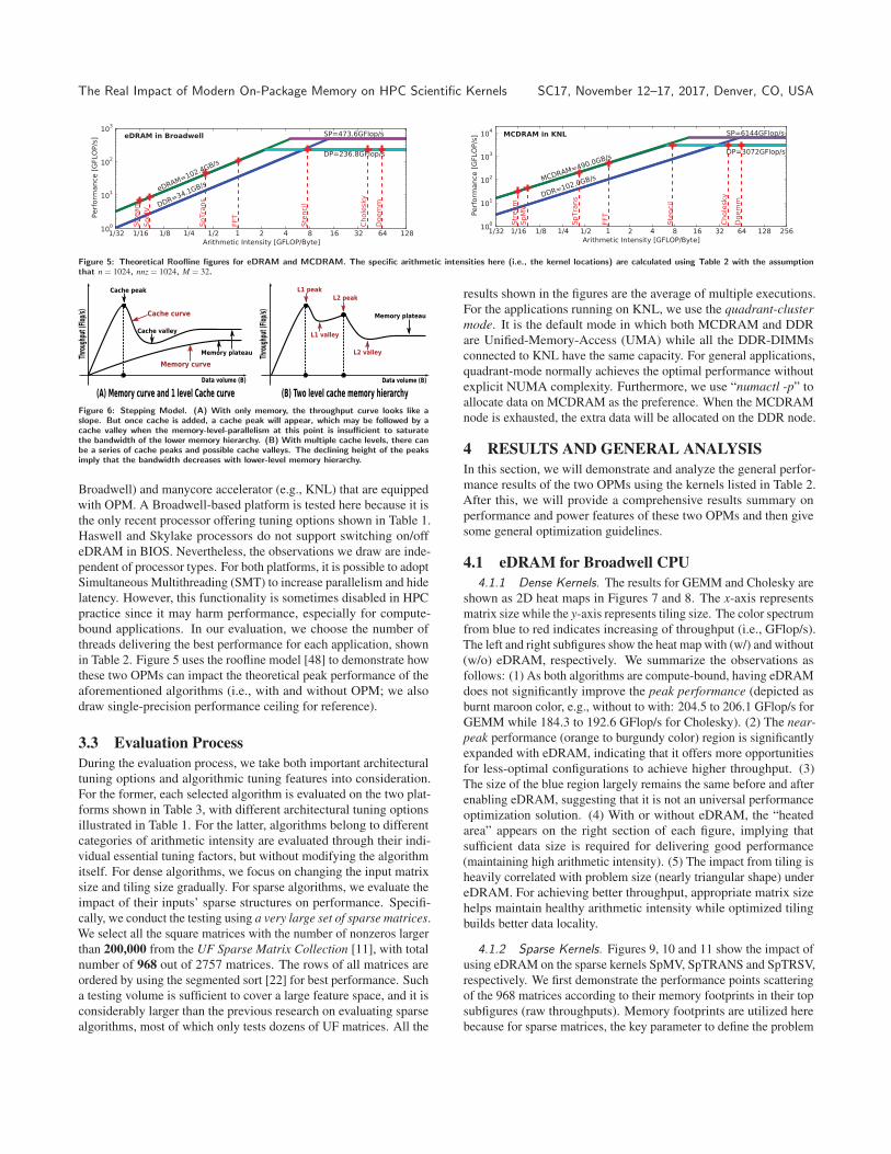
Figure 5: Theoretical Roofline figures for eDRAM and MCDRAM. The specific arithmetic intensities here (i.e., the kernel locations) are calculated using Table 2 with the assumptionthat n = 1024, nnz = 1024, M = 32.
Figure 6: Stepping Model. (A) With only memory, the throughput curve looks like aslope. But once cache is added, a cache peak will appear, which may be followed by acache valley when the memory-level-parallelism at this point is insufficient to saturatethe bandwidth of the lower memory hierarchy. (B) With multiple cache levels, there canbe a series of cache peaks and possible cache valleys. The declining height of the peaksimply that the bandwidth decreases with lower-level memory hierarchy.
Broadwell) and manycore accelerator (e.g., KNL) that are equipped
with OPM. A Broadwell-based platform is tested here because it is
the only recent processor offering tuning options shown in Table 1.
Haswell and Skylake processors do not support switching on/off
eDRAM in BIOS. Nevertheless, the observations we draw are inde-
pendent of processor types. For both platforms, it is possible to adopt
Simultaneous Multithreading (SMT) to increase parallelism and hide
latency. However, this functionality is sometimes disabled in HPC
practice since it may harm performance, especially for compute-
bound applications. In our evaluation, we choose the number of
threads delivering the best performance for each application, shown
in Table 2. Figure 5 uses the roofline model [48] to demonstrate how
these two OPMs can impact the theoretical peak performance of the
aforementioned algorithms (i.e., with and without OPM; we also
draw single-precision performance ceiling for reference).
3.3 Evaluation ProcessDuring the evaluation process, we take both important architectural
tuning options and algorithmic tuning features into consideration.
For the former, each selected algorithm is evaluated on the two plat-
forms shown in Table 3, with different architectural tuning options
illustrated in Table 1. For the latter, algorithms belong to different
categories of arithmetic intensity are evaluated through their indi-
vidual essential tuning factors, but without modifying the algorithm
itself. For dense algorithms, we focus on changing the input matrix
size and tiling size gradually. For sparse algorithms, we evaluate the
impact of their inputs’ sparse structures on performance. Specifi-
cally, we conduct the testing using a very large set of sparse matrices.
We select all the square matrices with the number of nonzeros larger
than 200,000 from the UF Sparse Matrix Collection [11], with total
number of 968 out of 2757 matrices. The rows of all matrices are
ordered by using the segmented sort [22] for best performance. Such
a testing volume is sufficient to cover a large feature space, and it is
considerably larger than the previous research on evaluating sparse
algorithms, most of which only tests dozens of UF matrices. All the
results shown in the figures are the average of multiple executions.
For the applications running on KNL, we use the quadrant-clustermode. It is the default mode in which both MCDRAM and DDR
are Unified-Memory-Access (UMA) while all the DDR-DIMMs
connected to KNL have the same capacity. For general applications,
quadrant-mode normally achieves the optimal performance without
explicit NUMA complexity. Furthermore, we use “numactl -p” to
allocate data on MCDRAM as the preference. When the MCDRAM
node is exhausted, the extra data will be allocated on the DDR node.
4 RESULTS AND GENERAL ANALYSISIn this section, we will demonstrate and analyze the general perfor-
mance results of the two OPMs using the kernels listed in Table 2.
After this, we will provide a comprehensive results summary on
performance and power features of these two OPMs and then give
some general optimization guidelines.
4.1 eDRAM for Broadwell CPU4.1.1 Dense Kernels. The results for GEMM and Cholesky are
shown as 2D heat maps in Figures 7 and 8. The x-axis represents
matrix size while the y-axis represents tiling size. The color spectrum
from blue to red indicates increasing of throughput (i.e., GFlop/s).
The left and right subfigures show the heat map with (w/) and without
(w/o) eDRAM, respectively. We summarize the observations as
follows: (1) As both algorithms are compute-bound, having eDRAM
does not significantly improve the peak performance (depicted as
burnt maroon color, e.g., without to with: 204.5 to 206.1 GFlop/s for
GEMM while 184.3 to 192.6 GFlop/s for Cholesky). (2) The near-peak performance (orange to burgundy color) region is significantly
expanded with eDRAM, indicating that it offers more opportunities
for less-optimal configurations to achieve higher throughput. (3)
The size of the blue region largely remains the same before and after
enabling eDRAM, suggesting that it is not an universal performance
optimization solution. (4) With or without eDRAM, the “heated
area” appears on the right section of each figure, implying that
sufficient data size is required for delivering good performance
(maintaining high arithmetic intensity). (5) The impact from tiling is
heavily correlated with problem size (nearly triangular shape) under
eDRAM. For achieving better throughput, appropriate matrix size
helps maintain healthy arithmetic intensity while optimized tiling
builds better data locality.
4.1.2 Sparse Kernels. Figures 9, 10 and 11 show the impact of
using eDRAM on the sparse kernels SpMV, SpTRANS and SpTRSV,
respectively. We first demonstrate the performance points scattering
of the 968 matrices according to their memory footprints in their top
subfigures (raw throughputs). Memory footprints are utilized here
because for sparse matrices, the key parameter to define the problem
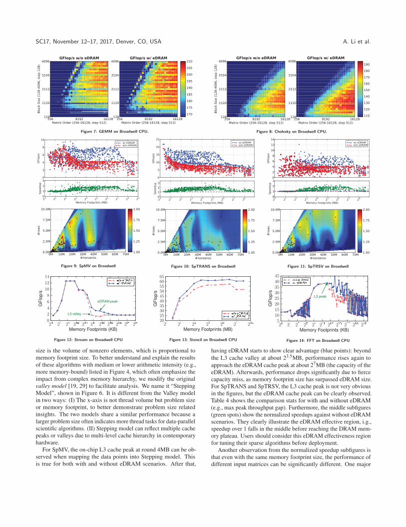
SC17, November 12–17, 2017, Denver, CO, USA A. Li et al.
Figure 7: GEMM on Broadwell CPU. Figure 8: Cholesky on Broadwell CPU.
Figure 9: SpMV on Broadwell Figure 10: SpTRANS on Broadwell Figure 11: SpTRSV on Broadwell
Figure 12: Stream on Broadwell CPU Figure 13: Stencil on Broadwell CPU Figure 14: FFT on Broadwell CPU
size is the volume of nonzero elements, which is proportional to
memory footprint size. To better understand and explain the results
of these algorithms with medium or lower arithmetic intensity (e.g.,
more memory-bound) listed in Figure 4, which often emphasize the
impact from complex memory hierarchy, we modify the original
valley model [19, 29] to facilitate analysis. We name it “Stepping
Model”, shown in Figure 6. It is different from the Valley model
in two ways: (I) The x-axis is not thread volume but problem size
or memory footprint, to better demonstrate problem size related
insights. The two models share a similar performance because a
larger problem size often indicates more thread tasks for data-parallel
scientific algorithms. (II) Stepping model can reflect multiple cache
peaks or valleys due to multi-level cache hierarchy in contemporary
hardware.
For SpMV, the on-chip L3 cache peak at round 4MB can be ob-
served when mapping the data points into Stepping model. This
is true for both with and without eDRAM scenarios. After that,
having eDRAM starts to show clear advantage (blue points): beyond
the L3 cache valley at about 23.5MB, performance rises again to
approach the eDRAM cache peak at about 27MB (the capacity of the
eDRAM). Afterwards, performance drops significantly due to fierce
capacity miss, as memory footprint size has surpassed eDRAM size.
For SpTRANS and SpTRSV, the L3 cache peak is not very obvious
in the figures, but the eDRAM cache peak can be clearly observed.
Table 4 shows the comparison stats for with and without eDRAM
(e.g., max peak throughput gap). Furthermore, the middle subfigures
(green spots) show the normalized speedups against without eDRAM
scenarios. They clearly illustrate the eDRAM effective region, i.g.,
speedup over 1 falls in the middle before reaching the DRAM mem-
ory plateau. Users should consider this eDRAM effectiveness region
for tuning their sparse algorithms before deployment.
Another observation from the normalized speedup subfigures is
that even with the same memory footprint size, the performance of
different input matrices can be significantly different. One major
The Real Impact of Modern On-Package Memory on HPC Scientific Kernels SC17, November 12–17, 2017, Denver, CO, USA
reason causing this is the sparse matrix structure. Three bottom
subfigures show the heat maps of the speedups with respect to the
number of rows and nonzero entries for the tested sparse matrices.
As can be seen, the matrices’ sparse structures play an important role
in determining their throughputs. For SpMV, the peak performance
region (reddest area) concentrates at the lower-left corner, with the
lower region for the nonzero entries as well. For SpTRANS, the
peak performance region is for small matrices (both small number of
rows and nonzero entries). For SpTRSV, the peak region is for small
number of rows, but small to modest number of nonzero entries.
These observations generally match algorithm characteristics: both
SpMV and SpTRSV commonly reuse vectors of size m (i.e., the
number of rows) thus achieve higher speedups when the vectors are
smaller and can be cached better; SpTRANS has less data reuse thus
behave better when the whole problem size is smaller.
4.1.3 Other Algorithms. Figures 12, 13 and 14 show the perfor-
mance results for Stream, Stencil and FFT, respectively. The x-axis
of these figures is log scaled. For Stream, clear L2 and L3 cache
peaks can be observed for both with and without eDRAM. However,
without eDRAM, there is a L3 cache valley before the DRAM band-
width can be fully exploited at the plateau. With eDRAM, this valley
is avoided with an eDRAM cache peak being formed. This is then
followed by a dropping of throughput due to poor eDRAM hit rate.
For Stencil, the “iso3dfd” (the essential kernel) implementation is
optimized by vector folding and cache blocking, with the blocking
dimension as 64x64x96 (3MB). Thus, the total memory footprint
size on the Broadwell is approximately 24MB, which is significantly
larger than the 6MB L3 cache but is smaller than the eDRAM. This
explains the throughput curve of Stencil with eDRAM continuously
outperforms that without eDRAM. For FFT, it can be seen that the
L3 cache peak is at about 6MB, or 212.6 KB. After that, without
eDRAM shows a clear cache valley while with eDRAM offers an-
other performance “sweetspot” at the eDRAM cache peak (≈ 214
KB). Beyond this cache peak (after 217 KB or 128MB), the perfor-
mance drops and converges to the one without eDRAM. Table 4
shows the detailed stats for these kernels when enabling eDRAM.
4.2 Observations on MCDRAM of KNL4.2.1 Dense Kernels. The results for GEMM and Cholesky on
KNL are shown in Figures 15 and 16. The upper-left, upper-right,
lower-left and lower-right subfigures represent preferring DDR (i.e.,
without MCDRAM), using MCDRAM in cache mode, flat mode,
and hybrid mode, respectively. We have the following observations:
(I) Similar to the observations in eDRAM (Figure 7), using MC-
DRAM as cache does not significantly increase the peak throughput
of GEMM (i.e., without MCDRAM to cache mode: 1425.5 GFlop/s
to 1483.4 GFlop/s) because GEMM has been well blocked for on-
chip L2 cache, but it does expand the opportunities for more inputs
to reach higher throughput. However, this phenomenon does not ap-
ply to Cholesky in which the peak performance increases noticeably
due to suboptimal tiling for L2. (II) MCDRAM as flat memory can
significantly boost throughput before certain boundary (around the
center of x-axis), implying it can help small sized problems achieve
better throughput without requiring large problem size to maintain
high arithmetic intensity. However, beyond the boundary (around the
MCDRAM capacity of 16GB), the performance becomes extremely
poor for both GEMM and Cholesky. This is interesting because
general wisdom believes that the performance of using MCDRAM
should be better or at least the same as that without MCDRAM (i.e.,
only using DDR). However, our results show otherwise: when an
array is partially allocated on both MCDRAM and DDR, the perfor-
mance becomes extremely poor. We suspect this is due to: (a) the
significantly increased bus conflicts in the network of cores on KNL,
when fetching data from MCDRAM and DDR at the same time; and
(b) significant set conflict in L2 when two entries in DDR and MC-
DRAM are mapped to the same L2 cache set. Additional conflicts on
L2 also include dual ports support for DDR and MCDRAM, result-
ing in extra cache transactions (e.g., synchronization). (III) Another
interesting finding is that the hybrid mode can be more effective than
the pure cache mode, which is against existing knowledge [27]. This
is especially true for GEMM, in which the cache tiling technique
has ensured that the memory footprint in cache is smaller than 8GB
(the cache capacity of hybrid mode). As such, the other 8GB, when
employing as flat memory, can be more beneficial than as pure cache
since cache is not always hit and requires additional tag checking
overhead (note that the flat memory and cache in MCDRAM are
at the same memory hierarchy due to sharing the same physical
hardware). However, when the memory footprint size is larger than
8GB, the cache mode becomes a better choice. (IV) These figures
also demonstrate the advantage of using MCDRAM as cache since
hardware-managed cache can dynamically shift its scope with the
moving of the kernel’s hotspot region but the flat memory cannot.
In summary, if the data size is large (e.g., larger than MCDRAM
capacity), but the frequently accessed memory footprint size is small,
the hybrid mode (when footprint size < 8GB) or cache mode (when
footprint size ≥ 8GB) is a better choice.
4.2.2 Sparse Kernels. Figures 17, 18, and 19 illustrate the
results for running three sparse algorithms on KNL, including SpMV,
SpTRANS and SpTRSV, respectively. Similar to the demonstration
for eDRAM, we show raw performance, relative speedups (with
respect to without MCDRAM) and the impact from sparse structures.
SpMV: In the top subfigure for raw performance, SpMV’s L2
cache peak can be easily identified at around 32M. After that, the
four modes diverge. Without MCDRAM, the performance drops
dramatically and saturates at DRAM memory plateau. After experi-
encing a short L2 cache valley, the performance of the other three
modes climbs back to approach MCDRAM’s throughput peak. Since
the memory footprints for most sparse matrices from UF sparse ma-
trix collection are much smaller than 8GB (i.e., within the hybrid
mode cache capacity), it is difficult to distinguish the three modes
since they have not reached the potential state that can separate them
apart. This phenomenon also occurs for SpTRANS and SpTRSV.
Therefore, we only draw one heatmap to represent all three modes
using MCDRAM since they share similar impact from sparse struc-
tures. Figure 20 shows that SpMV performs well on KNL when the
number of rows is small due to efficient vector caching.
SpTRANS: The behavior for SpTRANS is completely different
from SpMV. Based on the speedup figures, MCDRAM modes do
not deliver clear performance benefit over DDR. This is because
SpTRANS code already targets L2 cache for optimal tiling, resulting
in negligible performance improvement when enabling MCDRAM
modes. SpTRANS’ heat map (Figure 21) shows that it performs
the best (reddest) when both the number of rows and nonzeros are
smaller. This is because SpTRANS has less data reuse thus behave
better when the whole problem size is smaller.

SC17, November 12–17, 2017, Denver, CO, USA A. Li et al.
Figure 15: GEMM on KNL Figure 16: Cholesky on KNL
Figure 17: SpMV on KNL. Figure 18: SpTRANS on KNL. Figure 19: SpTRSV on KNL.
Figure 20: Structure impact of SpMV on KNL. Figure 21: Structure impact of SpTRANS on KNL. Figure 22: Structure impact of SpTRSV on KNL.
SpTRSV: SpTRSV has the same arithmetic intensity as SpMV
but it has much lower peak throughput due to heavy input-defined
data dependency. Thus, SpTRSV has lower memory level paral-
lelism and bandwidth demand, making MCDRAM access latency
higher than DDR (Section 2.2). Reflected by the speedup subfig-
ure in the middle (e.g., below 1 when memory footprint is larger),
whether enabling MCDRAM modes is better than DDR depends
on if the algorithm is latency bound (worse than DDR) or memory
bandwidth bound (better than DDR). Shown in the heatmap (Figure
22, a small number of rows and a moderate number of nonzeros in
SpTRSV benefit performance greatly due to better vector caching.
4.2.3 Other Kernels. The figures for Stream, Stencil and FFTare shown in Figures 23, 24, and 25, respectively. As can be seen,
the figure for Stream matches the Stepping model very well. The
L2 cache peak appears at about 32MB. All the four modes converge
before this point but diverge thereafter. We can also observe that
DDR mode’s performance quickly drops to the DRAM plateau after
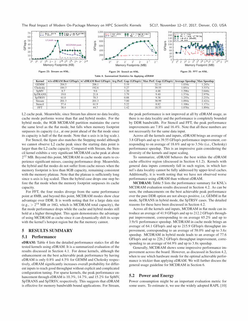
The Real Impact of Modern On-Package Memory on HPC Scientific Kernels SC17, November 12–17, 2017, Denver, CO, USA
Figure 23: Stream on KNL. Figure 24: Stencil on KNL. Figure 25: FFT on KNL.
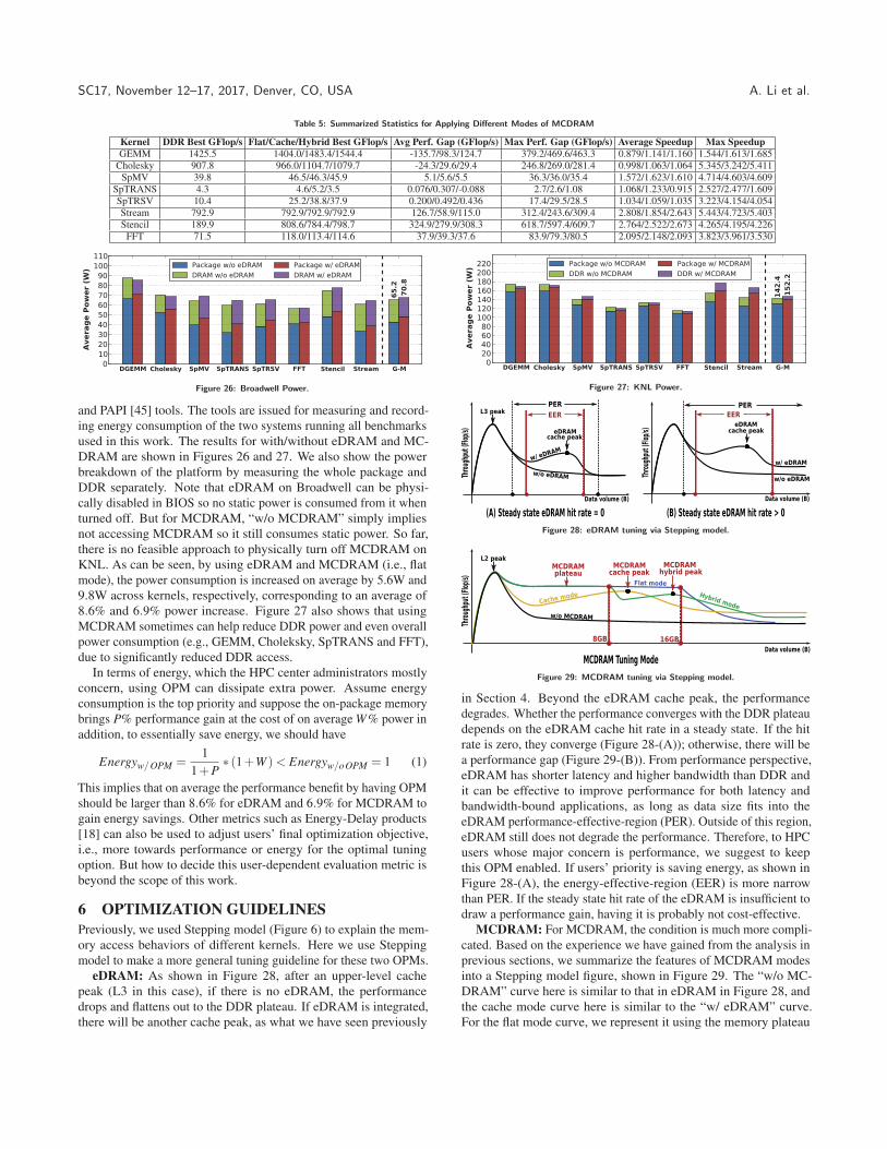
Table 4: Summarized Statistics for Applying eDRAM
Kernel w/o eDRAM Best GFlop/s w/ eDRAM Best GFlop/s Avg Perf. Gap (GFlop/s) Max Perf. Gap (GFlop/s) Average Speedup Max SpeedupGEMM 204.5 206.1 5.19 32.14 1.034x 1.243x
Cholesky 184.3 192.6 5.27 39.55 1.051x 3.537xSpMV 8.7 9.6 1.20 4.48 1.296x 2.644x
SpTRANS 19.0 21.8 3.79 9.40 1.574x 2.979xSpTRSV 61.0 70.3 0.88 9.38 1.255x 2.233xStream 201.3 201.3 7.00 38.99 1.094x 2.421xStencil 57.4 61.9 5.22 8.82 1.106x 1.171x
FFT 38.4 44.7 1.42 18.55 1.076x 1.894x
L2 cache peak. Meanwhile, since Stream has almost no data locality,
cache mode performs worse than flat and hybrid modes. For the
hybrid mode, the 8GB MCDRAM partition maintains the curve
the same level as the flat mode, but falls when memory footprint
surpasses its capacity (i.e., at one point ahead of the flat mode since
its capacity is half of the flat mode. Note that x-axis is in log scale.).
For Stencil, the figure also matches the Stepping model although
we cannot observe L2 cache peak since the starting data point is
larger than the L2 cache capacity. Compared with Stream, the Sten-
cil kernel exhibits a very significant MCDRAM cache peak at about
212 MB. Beyond this point, MCDRAM in cache mode starts to ex-
perience significant misses, causing performance drop. Meanwhile,
the hybrid and flat modes do not suffer from cache misses when the
memory footprint is less than 8GB capacity, remaining consistent
with the memory plateau. Note that the plateau is sufficiently long
since x-axis is log scaled. Then the hybrid case drops one step be-
fore the flat mode when the memory footprint surpasses its cache
capacity.
For FFT, the four modes diverge from the same performance
point at 8MB, and beyond this point, MCDRAM modes show clear
advantage over DDR. It is worth noting that for a large data size
(e.g., > 214 MB or 16G, which is MCDRAM total capacity), the
flat mode performance drops while the cache and hybrid modes still
hold at a higher throughput. This again demonstrates the advantage
of using MCDRAM as cache since it can dynamically shift its scope
with the kernel’s hotspot region but the flat memory cannot.
5 RESULTS SUMMARY5.1 PerformanceeDRAM: Table 4 lists the detailed performance statics for all the
tested kernels using eDRAM. It is a summarized evaluation of the
results discussed in Section 4.1. For dense kernels, although the
enhancement on the best achievable peak performance by having
eDRAM is only 0.8% and 4.5% for GEMM and Cholesky respec-
tively, eDRAM significantly increases overall probability for differ-
ent inputs to reach good throughput without explicit and complicated
configuration tuning. For sparse kernels, the peak performance en-
hancement through eDRAM is 10.3%, 14.7%, and 15.2% for SpMV,
SpTRANS and SpTRSV, respectively. This suggests that eDRAM
is effective for memory bandwidth bound applications. For Stream,
the peak performance is not improved at all by eDRAM usage, as
there is no data locality and the performance is completely bounded
by DDR bandwidth. For Stencil and FFT, the peak performance
improvements are 7.8% and 16.4%. Note that all these numbers are
not necessarily for the same data input.
Across all the kernels and inputs, eDRAM brings an average of
3.8 GFlop/s and up to 39.55 GFlop/s performance improvement, cor-
responding to on average of 18.6% and up to 3.54x (i.e., Cholesky)
performance speedup. This is an impressive gain considering the
diversity of the kernels and input scaling.
To summarize, eDRAM behaves the best within the eDRAM
cache effective region (discussed in Section 4.1.2). Kernels with
general data inputs commonly fall in such region, in which ker-
nel’s data locality cannot be fully addressed by upper-level caches.
Additionally, it is worth noting that we have not observed worse
performance using eDRAM than without eDRAM.
MCDRAM: Table 5 lists the performance summary for KNL’s
MCDRAM evaluation results discussed in Section 4.2. As can be
seen, the enhancements on the best achievable peak performance
over the pure DDR option are not always positive, i.e, GEMM in flat
mode, SpTRANS in hybrid mode, the SpTRSV cases. The detailed
reasons for these have been discussed in Section 4.2.
Across all the kernels and inputs, MCDRAM in flat mode can in-
troduce an average of 41.9 GFlop/s and up to 212.2 GFlop/s through-
put improvement, corresponding to on average 65.2% and up to
3.9x% performance speedup. MCDRAM in cache mode brings an
average of 64.1 GFlop/s and up to 215.9 GFlop/s throughput im-
provement, corresponding to an average of 58.0% and up to 3.6xspeedup. MCDRAM in hybrid mode leads to an average of 77.6
GFlop/s and up to 226.2 GFlop/s throughput improvement, corre-
sponding to an average of 64.9% and up to 3.8x speedup.
Generally, MCDRAM shows some impressive performance im-
provement across the board. However, as discussed in Section 4.2,
when to use which hardware mode for the optimal achievable perfor-
mance is trickier than applying eDRAM. We will further discuss the
general usage guideline for MCDRAM in Section 6.
5.2 Power and EnergyPower consumption might be an important evaluation metric for
some users. To estimate it, we use the widely adopted RAPL [10]
SC17, November 12–17, 2017, Denver, CO, USA A. Li et al.
Table 5: Summarized Statistics for Applying Different Modes of MCDRAM
Kernel DDR Best GFlop/s Flat/Cache/Hybrid Best GFlop/s Avg Perf. Gap (GFlop/s) Max Perf. Gap (GFlop/s) Average Speedup Max SpeedupGEMM 1425.5 1404.0/1483.4/1544.4 -135.7/98.3/124.7 379.2/469.6/463.3 0.879/1.141/1.160 1.544/1.613/1.685
Cholesky 907.8 966.0/1104.7/1079.7 -24.3/29.6/29.4 246.8/269.0/281.4 0.998/1.063/1.064 5.345/3.242/5.411SpMV 39.8 46.5/46.3/45.9 5.1/5.6/5.5 36.3/36.0/35.4 1.572/1.623/1.610 4.714/4.603/4.609
SpTRANS 4.3 4.6/5.2/3.5 0.076/0.307/-0.088 2.7/2.6/1.08 1.068/1.233/0.915 2.527/2.477/1.609SpTRSV 10.4 25.2/38.8/37.9 0.200/0.492/0.436 17.4/29.5/28.5 1.034/1.059/1.035 3.223/4.154/4.054Stream 792.9 792.9/792.9/792.9 126.7/58.9/115.0 312.4/243.6/309.4 2.808/1.854/2.643 5.443/4.723/5.403Stencil 189.9 808.6/784.4/798.7 324.9/279.9/308.3 618.7/597.4/609.7 2.764/2.522/2.673 4.265/4.195/4.226
FFT 71.5 118.0/113.4/114.6 37.9/39.3/37.6 83.9/79.3/80.5 2.095/2.148/2.093 3.823/3.961/3.530
Figure 26: Broadwell Power. Figure 27: KNL Power.
and PAPI [45] tools. The tools are issued for measuring and record-
ing energy consumption of the two systems running all benchmarks
used in this work. The results for with/without eDRAM and MC-
DRAM are shown in Figures 26 and 27. We also show the power
breakdown of the platform by measuring the whole package and
DDR separately. Note that eDRAM on Broadwell can be physi-
cally disabled in BIOS so no static power is consumed from it when
turned off. But for MCDRAM, “w/o MCDRAM” simply implies
not accessing MCDRAM so it still consumes static power. So far,
there is no feasible approach to physically turn off MCDRAM on
KNL. As can be seen, by using eDRAM and MCDRAM (i.e., flat
mode), the power consumption is increased on average by 5.6W and
9.8W across kernels, respectively, corresponding to an average of
8.6% and 6.9% power increase. Figure 27 also shows that using
MCDRAM sometimes can help reduce DDR power and even overall
power consumption (e.g., GEMM, Choleksky, SpTRANS and FFT),
due to significantly reduced DDR access.
In terms of energy, which the HPC center administrators mostly
concern, using OPM can dissipate extra power. Assume energy
consumption is the top priority and suppose the on-package memory
brings P% performance gain at the cost of on average W% power in
addition, to essentially save energy, we should have
Energyw/OPM =1
1+P∗ (1+W ) < Energyw/oOPM = 1 (1)
This implies that on average the performance benefit by having OPM
should be larger than 8.6% for eDRAM and 6.9% for MCDRAM to
gain energy savings. Other metrics such as Energy-Delay products
[18] can also be used to adjust users’ final optimization objective,
i.e., more towards performance or energy for the optimal tuning
option. But how to decide this user-dependent evaluation metric is
beyond the scope of this work.
6 OPTIMIZATION GUIDELINESPreviously, we used Stepping model (Figure 6) to explain the mem-
ory access behaviors of different kernels. Here we use Stepping
model to make a more general tuning guideline for these two OPMs.
eDRAM: As shown in Figure 28, after an upper-level cache
peak (L3 in this case), if there is no eDRAM, the performance
drops and flattens out to the DDR plateau. If eDRAM is integrated,
there will be another cache peak, as what we have seen previously
Figure 28: eDRAM tuning via Stepping model.
Figure 29: MCDRAM tuning via Stepping model.
in Section 4. Beyond the eDRAM cache peak, the performance
degrades. Whether the performance converges with the DDR plateau
depends on the eDRAM cache hit rate in a steady state. If the hit
rate is zero, they converge (Figure 28-(A)); otherwise, there will be
a performance gap (Figure 29-(B)). From performance perspective,
eDRAM has shorter latency and higher bandwidth than DDR and
it can be effective to improve performance for both latency and
bandwidth-bound applications, as long as data size fits into the
eDRAM performance-effective-region (PER). Outside of this region,
eDRAM still does not degrade the performance. Therefore, to HPC
users whose major concern is performance, we suggest to keep
this OPM enabled. If users’ priority is saving energy, as shown in
Figure 28-(A), the energy-effective-region (EER) is more narrow
than PER. If the steady state hit rate of the eDRAM is insufficient to
draw a performance gain, having it is probably not cost-effective.
MCDRAM: For MCDRAM, the condition is much more compli-
cated. Based on the experience we have gained from the analysis in
previous sections, we summarize the features of MCDRAM modes
into a Stepping model figure, shown in Figure 29. The “w/o MC-
DRAM” curve here is similar to that in eDRAM in Figure 28, and
the cache mode curve here is similar to the “w/ eDRAM” curve.
For the flat mode curve, we represent it using the memory plateau
The Real Impact of Modern On-Package Memory on HPC Scientific Kernels SC17, November 12–17, 2017, Denver, CO, USA
Figure 30: Example: tuning eDRAM hardware for throughput.
shape since all accesses are essentially hits. As discussed in Sec-
tion 4.2.1, its performance drops sharply beyond the memory capac-
ity, e.g.,16GB for flat mode. For the hybrid curve, before allocated
cache capacity (e.g., 8GB), it has very similar throughput as flat
mode. Before the data volume reaching to full MCDRAM capac-
ity, it has slightly worse performance than flat mode but does have
a cache peak (marked as MCDRAM hybrid peak in Figure 29).
From Figure 29, we have the following guidelines: (I) The “w/o
MCDRAM” curve generally shows the worst performance. One
exception is for flat mode, when the data allocation occur on both
MCDRAM and DDR, generating high NoC conflicts and upper-level
cache thrashing; (II) Flat mode shows the best performance when
the application data set is ensured to be less than MCDRAM’s ca-
pacity (all hits); (III) Hybrid mode shows its advantage when the
most-frequently-used memory footprint size is less than the allo-
cated cache size in the MCDRAM but the data size itself is larger
than the MCDRAM total capacity. Under this condition, hybrid
mode shows superior performance than both flat mode and cache
mode, as seen in the GEMM example. (IV) Cache mode behaves
the best when the data size cannot fit into MCDRAM capacity and
the most-frequently-used memory footprint size is larger than the
allocate cache size in the hybrid mode. This condition mostly occurs
for large problem size with relatively good locality. Note that we
do not analyze energy consumption tradeoff for MCDRAM due
to the mixed average power results in Figure 27 and the fact that
MCDRAM on the current KNL cannot be disabled.
Tuning OPM Hardware for Performance: Using the Stepping
model, we can also theoretically analyze how to tune the OPM
hardware for better performance. Using eDRAM as an example,
Figures 30-(A) and (B) show the results of increasing OPM cache
capacity and cache bandwidth. As can be seen, increasing OPM
cache size scales the cache peak while increasing OPM bandwidth
amplifies the peak.
7 RELATED WORKScientific kernels are the essential building blocks for today’s major
applications running in large-scale HPC environments, which often
consume tremendous execution cycles and resources. Analyzing the
performance of these scientific kernels on state-of-the-art emerging
architectures thus becomes a critical task, as it offers useful insights
on the potential of these latest hardware on performance boosting
as well as how to further optimize them. Such type of studies pre-
viously have been performed on Cell processor [47], GPGPU [7],
cloud servers [24], IBM Power-8 [2], Intel Xeon Phi Knights-Cornor
[26], etc. Most of these studies were focusing on processors. How-
ever, the last two decades’ practice in HPC has already shown that
memory effects are becoming the most prominent limiting factor for
continuous performance scaling towards exascale [13]. Therefore,
analyzing the performance impact from advances in memory tech-
nology (such as on-package memory) on scientific kernels becomes
a mission critical task for the HPC community.
In this work, we conducted an extensive study on two popular
OPMs: eDRAM and MCDRAM. In terms of eDRAM, the major-
ity of the existing works focus on either optimizing the memory
cell structure of eDRAM for low-power [9], energy-efficient error-
encoding scheme [46], or minimizing refresh operations of eDRAM
[3, 6]. Mittal et. al. [38, 37] provided surveys for embedded DRAM
and DRAM caches. For MCDRAM, since Intel KNL is a recently
released architecture, only less work has been conducted to measure
and optimize for particular algorithms, e.g., accelerating sparse ten-
sor factorization [41] and seismology software on KNL [21]. Some
other work [12] tried to model KNL performance using the classic
roofline model. However, no existing work has provided a compre-
hensive study targeting modern on-package memory and analyzing
their performance/power impact for critical scientific kernels. Fur-
thermore, none of them particularly emphasize the impact from the
recently released MCDRAM.
8 CONCLUSIONS AND FUTURE WORKIn this paper, we conduct a thorough empirical evaluation for the
impact of modern OPM on important HPC scientific kernels. We
evaluate different tuning modes of OPM and how they affect the
application turning for best throughput. To better understand all
the observations, we drive a visual analytic model from the valley
model and use it to explain the interaction between OPM archi-
tecture effects and kernels’ tuning features. Finally, we provide a
general optimization guideline on how to tune application and ar-
chitecture for best performance on platforms equipped with these
two OPM. Several interesting insights have been obtained through
our evaluation, e.g., how sparse structures affect throughput with
OPM, whether eDRAM is cost effective for different applications,
and under what circumstances hybrid MCDRAM can outperform
the other two options.
In future, we plan to investigate whether the configurations of the
OS, libraries, compilers and other features could have a noteworthy
impact on the overall system performance under OPM. For example,
so far we have tested all the kernels on CentOS-7.2 and it would
be interesting to explore the OS impact on performance and power.
There are several interesting research directions regarding OS, in-
cluding (1) under a multi-user/multi-application scenario (less likely
for HPC), how would OS distribute the OPM resources among appli-
cations based on fairness, efficiency and consistency; (2) in a virtual
environment, how would the host OS manage OPM across different
guest OS; (3) would OPM be useful for certain OS functionalities,
e.g., buffering page table? This work serves as an initial study on
OPM-related research in HPC and including a more diverse range
of impact factors can definitely expand the current research scope.
ACKNOWLEDGMENTSThis research is supported by U.S. DOE Office of Science, Office
of Advanced Scientific Computing Research, under the “CENATE”
project (award No. 66150), the European Union’s Horizon 2020
research and innovation programme under the Marie Sklodowska-
Curie “TICOH” project (grant No. 752321), and NSF XPS program
(grant CCF-1337131). The Pacific Northwest National Laboratory
is operated by Battelle for the U.S. Department of Energy under
contract DE-AC05-76RL01830.
SC17, November 12–17, 2017, Denver, CO, USA A. Li et al.
REFERENCES[1] 2016 november top500 list. https://www.top500.org/lists/2016/11/, 2016.[2] A. V. Adinetz, P. F. Baumeister, H. Bottiger, T. Hater, T. Maurer, D. Pleiter,
W. Schenck, and S. F. Schifano. Performance Evaluation of Scientific Applicationson POWER8. In High Performance Computing Systems. Performance Modeling,Benchmarking, and Simulation: 5th International Workshop, PMBS 2014., pages24–45, 2015.
[3] A. Agrawal, P. Jain, A. Ansari, and J. Torrellas. Refrint: Intelligent Refreshto Minimize Power in On-Chip Multiprocessor Cache Hierarchies. In 2013IEEE 19th International Symposium on High Performance Computer Architecture(HPCA), pages 400–411, 2013.
[4] E. Agullo, J. Demmel, J. Dongarra, B. Hadri, J. Kurzak, J. Langou, H. Ltaief,P. Luszczek, and S. Tomov. Numerical Linear Algebra on Emerging Architectures:The PLASMA and MAGMA Projects. Journal of Physics: Conference Series,180(1):012037, 2009.
[5] A. Buttari, J. Langou, J. Kurzak, and J. Dongarra. A Class of Parallel TiledLinear Algebra Algorithms for Multicore Architectures. Parallel Computing,35(1):38–53, 2009.
[6] M. Chang, P. Rosenfeld, S. Lu, and B. Jacob. Technology Comparison forLarge Last-level Caches (L3Cs): Low-leakage SRAM, Low Write-energy STT-RAM, and Refresh-optimized eDRAM. In Proceedings of the 2013 IEEE 19thInternational Symposium on High Performance Computer Architecture, HPCA’13, pages 143–154, 2013.
[7] S. Che, M. Boyer, J. Meng, D. Tarjan, J. W. Sheaffer, and K. Skadron. APerformance Study of General-Purpose Applications on Graphics ProcessorsUsing CUDA. J. Parallel Distrib. Comput., 68(10):1370–1380, 2008.
[8] K. C. Chun, P. Jain, J. H. Lee, and C. H. Kim. A sub-0.9V logic-compatibleembedded DRAM with boosted 3T gain cell, regulated bit-line write scheme andPVT-tracking read reference bias. In 2009 Symposium on VLSI Circuits, pages134–135, 2009.
[9] K. C. Chun, P. Jain, J. H. Lee, and C. H. Kim. A 3T Gain Cell Embedded DRAMUtilizing Preferential Boosting for High Density and Low Power On-Die Caches.IEEE Journal of Solid-State Circuits, 46(6):1495–1505, 2011.
[10] H. David, E. Gorbatov, U. R. Hanebutte, R. Khanna, and C. Le. RAPL: MemoryPower Estimation and Capping. In Proceedings of the 16th ACM/IEEE Inter-national Symposium on Low Power Electronics and Design, pages 189–194,2010.
[11] T. A. Davis and Y. Hu. The University of Florida Sparse Matrix Collection. ACMTrans. Math. Softw., 38(1):1:1–1:25, 2011.
[12] D. Doerfler, J. Deslippe, S. Williams, L. Oliker, B. Cook, T. Kurth, M. Lobet,T. M. Malas, J. Vay, and H. Vincenti. Applying the Roofline Performance Modelto the Intel Xeon Phi Knights Landing Processor. In ISC Workshops, 2016.
[13] J. Dongarra et al. The International Exascale Software Project Roadmap. Int. J.High Perform. Comput. Appl., 25(1):3–60, 2011.
[14] E. J. Fluhr et al. POWER8: A 12-core Server-Class Processor in 22nm SOI with7.6Tb/s Off-Chip Bandwidth. In 2014 IEEE International Solid-State CircuitsConference Digest of Technical Papers, pages 96–97, 2014.
[15] J. Barth et al. A 500 MHz Random Cycle, 1.5 ns Latency, SOI Embedded DRAMMacro Featuring a Three-Transistor Micro Sense Amplifier. IEEE Journal ofSolid-State Circuits, 43(1):86–95, 2008.
[16] P. Hammarlund et al. Haswell: The Fourth-Generation Intel Core Processor. IEEEMicro, 34(2):6–20, 2014.
[17] M. Frigo and S. G Johnson. The Design and Implementation of FFTW3. Pro-ceedings of the IEEE, 93(2):216–231, 2005.
[18] R. Ge, X. Feng, and K. W. Cameron. Performance-Constrained Distributed DVSScheduling for Scientific Applications on Power-aware Clusters. In Supercom-puting, 2005. Proceedings of the ACM/IEEE SC 2005 Conference, pages 34–45,2005.
[19] Z. Guz, E. Bolotin, I. Keidar, A. Kolodny, A. Mendelson, and U. C. Weiser. Many-Core vs. Many-Thread Machines: Stay Away From the Valley. IEEE ComputerArchitecture Letters, 8(1):25–28, 2009.
[20] A. Hartstein, V. Srinivasan, T. R. Puzak, and P. G. Emma. Cache Miss Behavior:
Is It√
2. In Proceedings of the 3rd Conference on Computing Frontiers, pages313–320, 2006.
[21] A. Heinecke, A. Breuer, M. Bader, and P. Dubey. High Order Seismic Simulationson the Intel Xeon Phi Processor (Knights Landing). In High Performance Com-puting: 31st International Conference, ISC High Performance 2016, Proceedings,pages 343–362, 2016.
[22] K. Hou, W. Liu, H. Wang, and W. Feng. Fast Segmented Sort on GPUs. InProceedings of the International Conference on Supercomputing, ICS ’17, pages12:1–12:10, 2017.
[23] K. Hou, H. Wang, and W. Feng. GPU-UniCache: Automatic Code Generationof Spatial Blocking for Stencils on GPUs. In Proceedings of the ComputingFrontiers Conference, CF’17, pages 107–116, 2017.
[24] A. Iosup, S. Ostermann, M. N. Yigitbasi, R. Prodan, T. Fahringer, and D. Epema.Performance Analysis of Cloud Computing Services for Many-Tasks ScientificComputing. IEEE Transactions on Parallel and Distributed Systems, 22(6):931–945, 2011.
[25] S. S. Iyer, J. E. Barth, P. C. Parries, J. P. Norum, J. P. Rice, L. R. Logan, andD. Hoyniak. Embedded DRAM: Technology platform for the Blue Gene/L chip.
IBM Journal of Research and Development, 49(2.3):333–350, 2005.[26] J. Jeffers and J. Reinders. Intel Xeon Phi coprocessor high-performance program-
ming. MK, 1st edition, 2013.[27] J. Jeffers, J. Reinders, and A. Sodani. Intel Xeon Phi Processor High Performance
Programming. MK, 2nd edition, 2016.[28] S. Junkins. The Compute Architecture of Intel Processor Graphics Gen8. Techni-
cal report, Intel Corp., 2015.[29] A. Li, S. L. Song, E. Brugel, A. Kumar, D. Chavarrıa-Miranda, and H. Corporaal.
X: A Comprehensive Analytic Model for Parallel Machines. In 2016 IEEEInternational Parallel and Distributed Processing Symposium (IPDPS), pages242–252, 2016.
[30] W. Liu. Parallel and Scalable Sparse Basic Linear Algebra Subprograms. PhDthesis, University of Copenhagen, 2015.
[31] W. Liu, A. Li, J. Hogg, I. S. Duff, and B. Vinter. A Synchronization-FreeAlgorithm for Parallel Sparse Triangular Solves. In Euro-Par 2016: Parallel Pro-cessing: 22nd International Conference on Parallel and Distributed Computing,Proceedings, pages 617–630, 2016.
[32] W. Liu and B. Vinter. A Framework for General Sparse Matrix-matrix Multiplica-tion on GPUs and Heterogeneous Processors. Journal of Parallel and DistributedComputing, 85:47–61, 2015.
[33] W. Liu and B. Vinter. CSR5: An Efficient Storage Format for Cross-PlatformSparse Matrix-Vector Multiplication. In Proceedings of the 29th ACM Interna-tional Conference on Supercomputing, ICS ’15, pages 339–350, 2015.
[34] W. Liu and B. Vinter. Speculative Segmented Sum for Sparse Matrix-VectorMultiplication on Heterogeneous Processors. Parallel Computing, 2015.
[35] W. Luk, J. Cai, R. Dennard, M. Immediato, and S. Kosonocky. A 3-TransistorDRAM Cell with Gated Diode for Enhanced Speed and Retention Time. In 2006Symposium on VLSI Circuits, 2006. Digest of Technical Papers., pages 184–185,2006.
[36] J. D. McCalpin. Memory Bandwidth and Machine Balance in Current High Per-formance Computers. IEEE Computer Society Technical Committee on ComputerArchitecture Newsletter, 1995.
[37] S. Mittal and J. S. Vetter. A Survey Of Techniques for Architecting DRAM Caches.IEEE Transactions on Parallel and Distributed Systems, 27(6):1852–1863, 2016.
[38] S. Mittal, J. S. Vetter, and D. Li. A Survey Of Architectural Approaches for Man-aging Embedded DRAM and Non-Volatile On-Chip Caches. IEEE Transactionson Parallel and Distributed Systems, 26(6):1524–1537, 2015.
[39] J. Park, M. Smelyanskiy, N. Sundaram, and P. Dubey. Sparsifying Synchro-nization for High-Performance Shared-Memory Sparse Triangular Solver. InSupercomputing: 29th International Conference, Proceedings, pages 124–140,2014.
[40] A. J. Smith. Cache Memories. ACM Comput. Surv., 14(3):473–530, 1982.[41] S. Smith, J. Park, and G. Karypis. Sparse Tensor Factorization on Many-Core
Processors with High-Bandwidth Memory. In 2017 IEEE International Paralleland Distributed Processing Symposium, IPDPS ’17, 2017.
[42] A. Sodani, R. Gramunt, J. Corbal, H. Kim, K. Vinod, S. Chinthamani, S. Hutsell,R. Agarwal, and Y. Liu. Knights Landing: Second-Generation Intel Xeon PhiProduct. IEEE Micro, 36(2):34–46, 2016.
[43] D. Somasekhar, Y. Ye, P. Aseron, S. L. Lu, M. Khellah, J. Howard, G. Ruhl,T. Karnik, S. Y. Borkar, V. De, and A. Keshavarzi. 2GHz 2Mb 2T Gain-CellMemory Macro with 128GB/s Bandwidth in a 65nm Logic Process. In 2008 IEEEInternational Solid-State Circuits Conference - Digest of Technical Papers, pages274–613, 2008.
[44] H. Wang, W. Liu, K. Hou, and W. Feng. Parallel Transposition of Sparse DataStructures. In Proceedings of the 2016 International Conference on Supercomput-ing, ICS ’16, pages 33:1–33:13, 2016.
[45] V. M. Weaver, M. Johnson, K. Kasichayanula, J. Ralph, P. Luszczek, D. Terpstra,and S. Moore. Measuring Energy and Power with PAPI. In Proceedings of the2012 41st International Conference on Parallel Processing Workshops, pages262–268, 2012.
[46] C. Wilkerson, A. R. Alameldeen, Z. Chishti, W. Wu, D. Somasekhar, and S. Lu.Reducing Cache Power with Low-cost, Multi-bit Error-correcting Codes. In Pro-ceedings of the 37th Annual International Symposium on Computer Architecture,ISCA ’10, pages 83–93, 2010.
[47] S. Williams, J. Shalf, L. Oliker, S. Kamil, P. Husbands, and K. Yelick. ThePotential of the Cell Processor for Scientific Computing. In Proceedings of the3rd Conference on Computing Frontiers, CF ’06, pages 9–20, 2006.
[48] S. Williams, A. Waterman, and D. Patterson. Roofline: An Insightful VisualPerformance Model for Multicore Architectures. Communications of the ACM,52(4):65–76, 2009.
[49] C. Yount, J. Tobin, A. Breuer, and A. Duran. YASK – Yet Another StencilKernel: A Framework for HPC Stencil Code-Generation and Tuning. In 2016Sixth International Workshop on Domain-Specific Languages and High-LevelFrameworks for High Performance Computing, pages 30–39, 2016.

The Real Impact of Modern On-Package Memory on HPC Scientific Kernels SC17, November 12–17, 2017, Denver, CO, USA
A APPENDIX: COMPUTATIONAL RESULTSANALYSIS OF KERNELS BENCHMARKED
This artifact comprises the system configuration of the two platforms
with on-package memories, and the source code links, datasets, and
algorithm parameters of the scientific kernels benchmarked in our
SC ’17 paper “Exploring and Analyzing the Real Impact of Modern
On-Package Memory on HPC Scientific Kernels”.
A.1 System ConfigurationThe two platforms, i.e., Intel Core i7-5775c (Broadwell, BRD for
short) and Xeon Phi 7210 (Knights Landing, KNL for short), are
configured exactly the same.
• Binary: OpenMP executables
• Compilation: GNU gcc v4.9.2; Intel icc v17.0.1
• Runtime environment: Intel Parallel Studio XE v2017.1.043;
Papi v5.5.1 (http://icl.cs.utk.edu/papi/software/view.html?
id=250)
• Operating system: 64-bit CentOS v7.3.1611, Linux kernel
version v3.10.0-514.6.1.el7.x86 64
Note that their hardware configurations are listed in Table 3.
A.2 Scientific KernelsA.2.1 General Matrix-Matrix Multiplication (GEMM).
• Package name: PLASMA (Parallel Linear Algebra Soft-
ware for Multicore Architectures)
• Publication: Emmanuel Agullo, Jim Demmel, Jack Don-
garra, Bilel Hadri, Jakub Kurzak, Julien Langou, Hatem
Ltaief, Piotr Luszczek, and Stanimire Tomov. Numerical
Linear Algebra on Emerging Architectures: The PLASMA
and MAGMA Projects. Journal of Physics: Conference
Series, 180(1):012037, 2009.
• Source code: https://bitbucket.org/icl/plasma
• Serial BLAS back-end: Intel MKL v2017 Update 1
• Dataset: Dense matrices of given size filled with randomly
generated values
• Executable argument: ./test dgemm --m=msz --n=msz--k=msz --nb=bsz, where msz is matrix size in ranges
{256 .. 16128 .. 512} and {256 .. 32000 .. 1024} on
BRD and KNL, respectively, and bsz is tiling size in range
{128 .. 4096 .. 128} on both platforms
• Output: Dataset statistics, elapsed execution time, GFLOPs
throughput
A.2.2 Cholesky Decomposition.
• Package name: PLASMA (Parallel Linear Algebra Soft-
ware for Multicore Architectures)
• Publication: Emmanuel Agullo, Jim Demmel, Jack Don-
garra, Bilel Hadri, Jakub Kurzak, Julien Langou, Hatem
Ltaief, Piotr Luszczek, and Stanimire Tomov. Numerical
Linear Algebra on Emerging Architectures: The PLASMA
and MAGMA Projects. Journal of Physics: Conference
Series, 180(1):012037, 2009.
• Source code: https://bitbucket.org/icl/plasma
• Serial BLAS back-end: Intel MKL v2017 Update 1
• Dataset: Dense matrices of given size filled with randomly
generated values
• Executable argument: ./test dpotrf --m=msz --n=msz--k=msz --nb=bsz, where msz is matrix size in ranges
{256 .. 16128 .. 512} and {256 .. 32000 .. 1024} on
BRD and KNL, respectively, and bsz is tiling size in range
{128 .. 4096 .. 128} on both platforms
• Output: Dataset statistics, elapsed execution time, GFLOPs
throughput
A.2.3 Sparse Matrix-Vector Multiplication (SpMV).
• Package name: Benchmark SpMV using CSR5
• Publication: Weifeng Liu and Brian Vinter. CSR5: An
Efficient Storage Format for Cross-Platform Sparse Matrix-
Vector Multiplication. In Proceedings of the 29th ACM In-
ternational Conference on Supercomputing, ICS ’15, pages
339–350, 2015.
• Source code: https://github.com/bhSPARSE/Benchmark
SpMV using CSR5
• Dataset: 968 matrices (in the matrix market format) from
the University of Florida Sparse Matrix Collection (https:
//www.cise.ufl.edu/research/sparse/matrices/)
• Executable argument: ./spmv matrix.mtx
• Output: Dataset statistics, elapsed execution time, GFLOPs
throughput
A.2.4 Sparse Matrix Transposition (SpTRANS).
• Package name: ScanTrans and MergeTrans (for BRD and
KNL, respectively)
• Publication: Hao Wang, Weifeng Liu, Kaixi Hou, and Wu-
chun Feng. Parallel Transposition of Sparse Data Structures.
In Proceedings of the 2016 International Conference on
Supercomputing, ICS ’16, pages 33:1–33:13, 2016.
• Source code: https://github.com/vtsynergy/sptrans
• Dataset: 968 matrices (in the matrix market format) from
the University of Florida Sparse Matrix Collection (https:
//www.cise.ufl.edu/research/sparse/matrices/). They are
transposed from the CSR to the CSC format.
• Executable argument: export VER=5 for BRD or export
VER=7 for KNL, then ./sptranspose matrix.mtx
• Output: Dataset statistics, elapsed execution time, GFLOPs
throughput
A.2.5 Sparse Triangular Solve (SpTRSV).
• Package name: SpMP (sparse matrix pre-processing li-
brary)
• Publication: Jongsoo Park, Mikhail Smelyanskiy, Narayanan
Sundaram, and Pradeep Dubey. Sparsifying Synchroniza-
tion for High- Performance Shared-Memory Sparse Trian-
gular Solver. In Supercomputing: 29th International Con-
ference, ISC 2014, Leipzig, Germany, June 22-26, 2014.
Proceedings, pages 124–140, 2014.
• Source code: https://github.com/IntelLabs/SpMP
• Dataset: 968 matrices (in the matrix market format) from
the University of Florida Sparse Matrix Collection (https:
//www.cise.ufl.edu/research/sparse/matrices/). Note that a
diagonal is added to any singular matrices in the list to
make them nonsingular, and the lower triangular part (i.e.,
forward substitution) is tested.
• Executable argument: ./trsv test matrix.mtx
SC17, November 12–17, 2017, Denver, CO, USA A. Li et al.
• Output: Dataset statistics, elapsed execution time, GFLOPs
throughput
A.2.6 Stencil.
• Package name: YASK (Yet Another Stencil Kernel)
• Publication: C. Yount, J. Tobin, A. Breuer, and A. Du-
ran. YASK – Yet Another Stencil Kernel: A Framework for
HPC Stencil Code Generation and Tuning. In 2016 Sixth In-
ternational Workshop on Domain-Specific Languages and
High-Level Frameworks for High Performance Computing
(WOLFHPC), pages 30–39, 2016.
• Source code: https://github.com/01org/yask
• Dataset: 3D grid of given size filled with randomly gener-
ated values
• Executable argument: First run make stencil=iso3dfd
arch=hsw (or knl) mpi=1, then run ./stencil-run.sh
-arch hsw (or knl) -nr 1 gridsz -b 64 -bz 96, where
gridsz is 3D grid size in ranges {32× 16× 16 .. 1024×1024×512 .. 2× size in each step} and {128×64×64 ..
20483 .. 2× size in each step} on BRD and KNL, respec-
tively
• Output: Dataset statistics, elapsed execution time, GFLOPs
throughput
A.2.7 Fast Fourier Transform (FFT).
• Package name: FFTW v3.3.5
• Publication: Matteo Frigo and Steven G Johnson. The
Design and Implementation of FFTW3. Proceedings of the
IEEE, 93(2):216–231, 2005.
• Source code: http://www.fftw.org/download.html
• Dataset: 3D dataset of given size filled with randomly
generated values
• Executable argument: ./bench -s irf(or orf, irb,
orb)sizexsizexsize -opatient -onthreads=8 (for BRD,
or 256 for KNL), where size is 3D dataset size in ranges
{96 .. 592 .. 16} and {96 .. 1088 .. 32} on BRD and KNL,
respectively
• Output: Dataset statistics, elapsed execution time, GFLOPs
throughput
A.2.8 Stream.
• Package name: Stream
• Publication: John D. McCalpin. Memory Bandwidth and
Machine Balance in Current High Performance Computers.
IEEE Computer Society Technical Committee on Computer
Architecture (TCCA) Newsletter, 1995.
• Source code: http://www.cs.virginia.edu/stream/ref.html
• Dataset: Array of given size filled with randomly generated
values
• Executable argument: First compile the code with icc
-O3 -xCORE-AVX2 -ffreestanding -qopenmp -mcmodel=medium
-DSTREAM ARRAY SIZE="arraysz" -DNTIMES="nrun" stream.c
-o stream.omp.AVX2.icc, where arraysz is array size in
ranges {24 .. 224 .. 2× size in each step} and {24 .. 226 ..
2× size in each step} on BRD and KNL, respectively, and
nrun is 2000 for arrays of small sizes and 20 for arrays of
large sizes. Then run ./stream.omp.AVX2.icc
• Output: Dataset statistics, elapsed execution time, GB/s
throughput
A.3 Raw Experimental ResultsWe uploaded our raw experimental data to a repository at Github.
The link can be found at:
https://github.com/bhSPARSE/opm rawdata.