Embed Size (px)
Citation preview
International Journal of Engineering & Technology IJET-IJENS Vol:14 No:02 32
143502-2727-IJET-IJENS © April 2014 IJENS I J E N S
Exploration Electromagnetic Noise Reduction
for IC Electric Field Measurement and
Prediction in GTEM Cell
King Lee Chua1, Mohd Zarar Mohd Jenu
1, Man On Wong
2, See Hour Ying
2
1Center for Electromagnetic Compatibility, Universiti Tun Hussein Onn Malaysia (UTHM),
Parit Raja, Batu Pahat, 86400 Johor, Malaysia.
[email protected], [email protected] 2Altera Corporation (M) Sdn. Bhd.
Plot 6, Bayan Lepas Technoplex, Medan Bayan Lepas, 11900, Penang, Malaysia.
[email protected], [email protected]
Abstract-- In IEC 61967 standards, there is often interest to
evaluate electromagnetic emission of integrated circuits (ICs) by
mounting IC test board on TEM/GTEM cell wall. The method is
able to separate the desired emission measurement to be
influenced by unintentional interference. However, this method
has limited test device rotation in horizontal position as well as
neglecting vertical polarization which is also a significant source
of emission. Basically, the electromagnetic emission of a device is
contributed by both the horizontal and vertical polarizations.
The limitation can be overcome with three dimensional views as
termed to be three orthogonal rotations in Gigahertz Transverse
Electromagnetic Mode (GTEM). When conduct emission
measurement by placing the whole test device in the GTEM cell,
it is important to ensure that unwanted disruption from
supporting components on the test board and its interface cable
will not interfere with the measurement. Therefore, in this paper,
we present numerous experimental works to tackle these crucial
matters in order to emphasize the technique to quantify IC
electromagnetic emission performed inside a GTEM cell. This is
achieved with application of basic electromagnetic compatibility
(EMC) measurement approaches such as shielding, grounding
and suppression using ferromagnetic material. Following that,
dipole moments model is established to achieve far electric field
approximation and verification with semi-anechoic chamber
(SAC) measurement. The results show strong evidence that the
effectiveness of the new proposed technique for IC emission
measurement in GTEM cell. The obtained results are then
processed further using conventional algorithm for correlation
with field measurement in semi anechoic chamber.
Index Term-- Electromagnetic noise, integrated circuit,
electromagnetic radiation, GTEM cell, SAC
1. INTRODUCTION
The electronic world nowadays is moving towards the fashion
for producing smaller devices with faster clock speed and
higher integration densities. This is generally realized by
embedding electronic components such as transistors, diodes,
capacitors and resistors in a miniature size integrated circuit
(IC). Due to advance semiconductor process technologies,
smaller ICs can be built with very complex structure.
Consequently, ICs have become significant noise source that
cause electromagnetic emission. The fact has led to growing
demands on electromagnetic emission characterization at chip
level. The exploration is importance to provide the
corresponding information for component selection in early
printed circuit board (PCB) design. Therefore, shorter time is
required to develop any electronic system in compliance of
electromagnetic compatibility (EMC) test.
According to the studies in past, two techniques namely
TEM/GTEM cell measurement method [1] and near field
scanning method [2] and [3] are introduced for ICs
electromagnetic emission characterization. Near field
technique has advantage to characterize IC electromagnetic
emission in close vicinity, with assumption the measured
emission is contributing by IC itself if an infinite perfect
ground plane is established around the IC test board. This
ensures IC is the only radiator and reliability of the
measurement is attained. Conversely, ambient noise may be
considered as the main aspect that disturbing measurement
accuracy in the near field method. To prevent disruption of the
ambient noise, the near field system generally is setup inside
shielding room which is costly and not affordable by most of
EMC test laboratories.
Basically, TEM/GTEM cell is an enclosed metallic
structure which provides well isolation between inner and
outer environments of the cell. As the cell is properly closed,
its inner side would neither contribute to nor suffer from any
external interference. The cell cost is also relatively cheaper
than building a shielding room. Another issue of the near field
method is field probe sensitivity must compromise with spatial
resolution and dynamic range. A narrow band probe merely
suitable for field measurement in a specific frequency range,
therefore various set of probes are needed for emission test in
different frequency ranges. In particular, TEM/GTEM cell
septum behaves as receiving antenna which has frequency
response over a wide band of frequency, so no receiving
antenna change is required. The GTEM cell can operate over
wider range of frequencies than TEM cell. In addition, GTEM
cell offers three dimensional field views which provide overall
information for radiated emission testing for the IC.
In this paper, the focus is given on the technique to
characterize radiated electromagnetic emission of a FPGA
chip using GTEM cell. The measurement is conducted inside

International Journal of Engineering & Technology IJET-IJENS Vol:14 No:02 33
143502-2727-IJET-IJENS © April 2014 IJENS I J E N S
the cell instead of clamping it on the cell body. In order to
ensure that the FPGA chip is continuously active in the
measurement, the chip was configured with toggle flip-flop
(TFF) pattern and exercised at a 100MHz clock signal. Several
techniques such as shielding the FPGA board inside a metallic
enclosure, grounding the enclosure with low impedance
ground strap and suppressing common mode current emission
of interface cables using ferromagnetic material are employed
to avoid interference due to unwanted electromagnetic noise.
Then, the GTEM data is process to extract equivalent dipole
moments for far field prediction and verification with SAC
measurement. The results presented in the study provide
useful alternative to IC emission test methods based on IEC
61967.
2. CHARACTERIZATION OF GTEM CELL
Prior to perform any electromagnetic emission measurement
of ICs, the performance of GTEM cell is important to be
checked and validated. This can ensure the measured data
achieve a reasonable level of accuracy.
GTEM cell can be considered as a rectangular
transmission line which operates in TEM mode. The cell
characteristic impedance Z0 along septum length is expected to
be 502. This parameter must be checked because
impedance mismatching can lead to multiple reflections and
eventually affect reliability and accuracy of collected raw
data. When a network analyzer is connected to cell port, it is
possible to evaluate the overall cell input impedance against
frequency range of interest. Fig. 1(a) shows the input
impedance over a frequency range from 30MHz up to 1GHz.
It is seen that the input impedance varies about 50
frequency of interest.
The reflection properties at GTEM cell is characterized
by measuring return loss of the cell when it is empty. As can
be seen in Fig. 1 (b), the return loss is well below 20dB over
the frequency spectrum. The 50 load and the RF absorber
have minimized reflections and resonances in the cell. The
return loss that exceeds -20dB still considered acceptable
because according to the standard IEC 61967-2, the return loss
ought to be below 14dB and it is equivalent to a VSWR value
of 1.5.
(a)
(b)
Fig. 1. Parameters of GTEM cell, (a) cell impedance vs frequency, and (b)
cell return loss
Basically, a GTEM cell comprises a tapered section with
a single port, 50 ohm characteristic impedance and a RF
absorber. Fig. 2(a) shows the setup of a spectrum analyzer to
measure output voltage due to electromagnetic emission of
any device under test (DUT) in the cell. In accordance to
transmission line theory, the overall structure can be
simplified into an equivalent circuit in Fig. 2(b). Here, it is
assumed that cell septum as inner conductor, cell wall as outer
conductor, the DUT represents a source and the spectrum
analyzer is the load.
(a)
50Ω Z0
l
Transmission line
VS
VLZL
ZS
Vi
z = -lz = 0
z
(b)
Fig. 2. (a) GTEM emission measurement setup,
(b) Equivalent circuit
Voltage reflection coefficient Γ at a load is defined as the
ratio of the amplitudes of the reflected and incident voltage
waves [4]. Assume the GTEM cell as lossless transmission
line, the voltage reflection coefficient can be obtained as
(1)
where is incident wave travelling towards the load,
represents reflected wave travelling towards the source, ZL is
100 200 300 400 500 600 700 800 900 100030
35
40
45
50
55
60
65
70
Frequency (MHz)
Imp
ed
an
ce
(O
hm
)
100 200 300 400 500 600 700 800 900 1000-70
-60
-50
-40
-30
-20
-10
Frequency (MHz)
S1
1 (
dB
)
Septum
RF absorber
50
load

International Journal of Engineering & Technology IJET-IJENS Vol:14 No:02 34
143502-2727-IJET-IJENS © April 2014 IJENS I J E N S
load impedance, Z0 is characteristic impedance, and zL is
normalized load impedance ⁄ . The magnitude of | ( )| at the load is obtained
| ( )| | ( )|
| |[ | | | | ( )]
⁄ (2)
with
phase constant, c is speed of light in free space,
| | is reflection coefficient, and is phase angle.
The voltage at source is determined with
| ( )| ( ) (3)
3. TEST DEVICE PREPARATION
The DUT chosen for emission test is a field programmable
gate array (FPGA) chip which is mounted on a printed circuit
board (PCB) and sitting on top of ground plane. All necessary
components, other than the chip, are soldered on opposite side
of the PCB. Fig. 3 shows the FPGA test board.
(a) (b)
Fig. 3. FPGA test board, (a) Top side, (b) Bottom side
It has been challenging to characterize electromagnetic
emission of IC inside the GTEM cell. This is because all
supporting components and interconnection cables on the PCB
may generate unwanted energy that would also couple to cell
septum. As a result, the measured emission is a combination
field contributed by the IC and the disturbance. However, it is
believe that the interference can be minimized if precautions
are taken into account in the measurement setup.
Shielding is a simple and effective technique that has
widely been used to isolate an environment from
electromagnetic interference. So the PCB is firstly housed
inside a metallic cavity and exposes the IC via a window.
Since conductor is a perfect shield, it can isolate unwanted
energy inside the cavity. This can ensure the FPGA chip is the
only source to contribute electromagnetic emission in
measurement.
In general, the performance of a shield depends on shield
thickness. According to [5], if shield thickness is greater than
skin depth of the material at the frequency of incident field,
there is less likely the multiple reflections and the material is
dominated by absorption loss, so it can behave as a good
solved by
√ ⁄ meter (4)
with f is frequency of incident field, is shield conductivity
and is shield permittivity. Aluminium is a cheap and
versatile conductor with adequate absorption for shield. Its
conductivity, is ⁄ , relative permittivity, is
and permeability, is ⁄ . When
aluminium is selected as shield material to build the cavity,
the skin depth for the lowest frequency of interest, 30MHz is
approximated 0.026mm. Since the shield thickness is 0.2mm,
so it can be assumed that the cavity is working as a perfect
barrier to isolate generated electromagnetic wave to travel
across once the cavity joints are properly shielded.
Although the conductor can behave as a good shield,
however, at the same time, it might be a perfect radiator if the
cavity resonant frequency fr agree with fundamental frequency
and harmonics of electromagnetic energy inside the cavity. In
this particular case, resonance may amplify the energy inside
the cavity and consequently propagate it out of the cavity. The
resonance frequency of the cavity can be determined by
√ √(
)
(
)
(
)
(5)
where
√ is phase velocity of uniform plane wave in the loss
less dielectric medium (=0, , ) filling the cavity, m, n and p
correspond to the number of half-wave variations of the field
in respective x-, y- and z-direction. The lowest resonant
frequency of the cavity is approximated 1.7GHz and it is
greater than the highest frequency of interest. Thus, as long as
the operating frequency and its harmonics stay below this
resonance frequency, the cavity will sustain a free oscillation.
The setup of the FPGA board in the metallic cavity is shown
in Fig. 4.
Fig. 4. Setup of the FPGA board inside metallic cavity
4. ELIMINATION ELECTROMAGNETIC NOISE
4.1. Ambient Noise
It is important to evaluate ambient noise inside the GTEM cell
to ensure that there are no external electromagnetic leakages
due to imperfect shielding of the cell. Therefore, action can be
taken if any voltage peak appears on the desired spectrum
frequency. This is to make sure what is measured is
contributed by the IC and a clean noise floor shall be obtained
when it is not powered.
a. Grounding
As mentioned previously, the cavity may be a good radiator if
not properly grounded. When the IC is energized, the
electromagnetic fields which emitted from package lead frame
and bonding wires of the IC will coupled with the cell septum.
International Journal of Engineering & Technology IJET-IJENS Vol:14 No:02 35
143502-2727-IJET-IJENS © April 2014 IJENS I J E N S
However, part of the fields will also be coupled with the
cavity, resulting in induction current which will produce
secondary emission.
In this case, proper grounding is extremely important for
diverting the current away from the cavity. Thus, the inner
side of the cavity is grounded to PCB using gasket whereas
the outer side is tied to GTEM cell body using ground strap.
The high quality ground strap has to be chosen to provide low
impedance and good bonding between connecting points to
avoid unwanted potential difference developed along the path.
The basic concept is lower impedance path will divert more
current away from the victim.
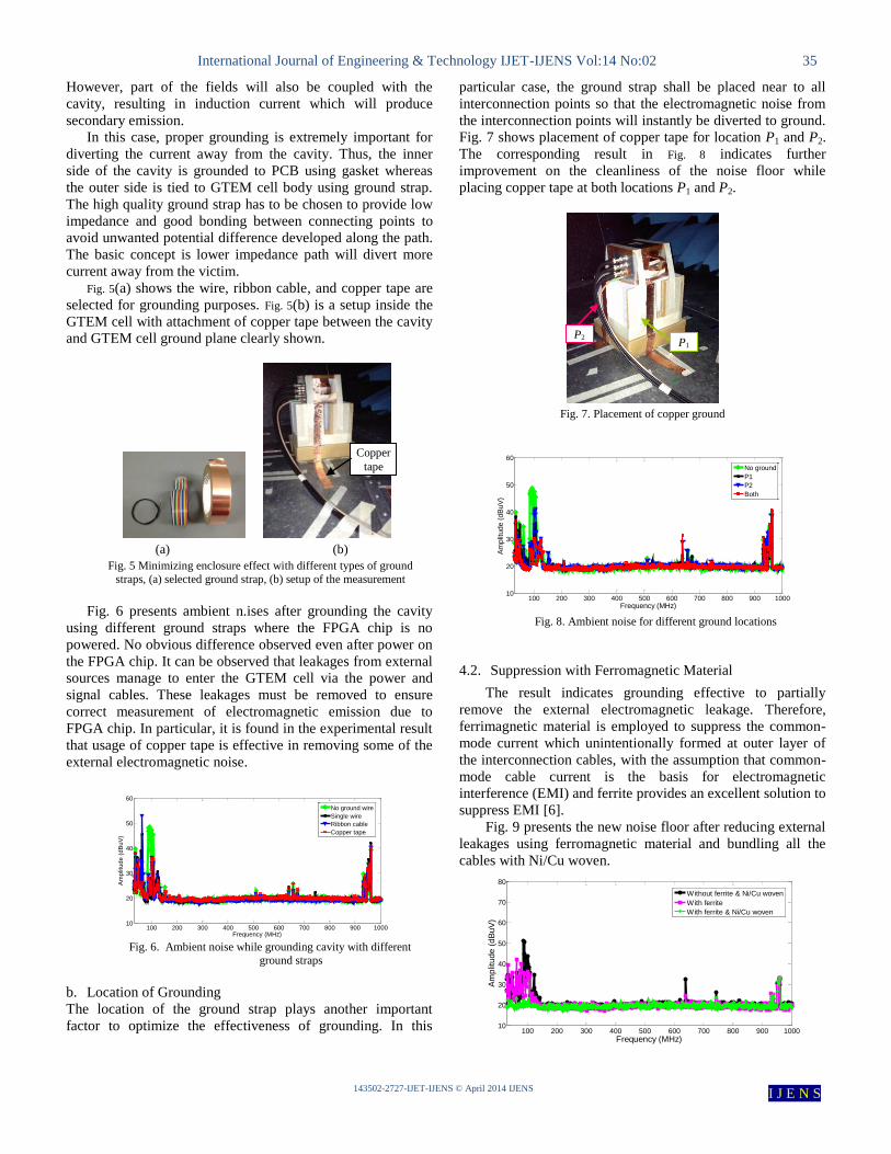
Fig. 5(a) shows the wire, ribbon cable, and copper tape are
selected for grounding purposes. Fig. 5(b) is a setup inside the
GTEM cell with attachment of copper tape between the cavity
and GTEM cell ground plane clearly shown.
(a) (b)
Fig. 5 Minimizing enclosure effect with different types of ground
straps, (a) selected ground strap, (b) setup of the measurement
Fig. 6 presents ambient n.ises after grounding the cavity
using different ground straps where the FPGA chip is no
powered. No obvious difference observed even after power on
the FPGA chip. It can be observed that leakages from external
sources manage to enter the GTEM cell via the power and
signal cables. These leakages must be removed to ensure
correct measurement of electromagnetic emission due to
FPGA chip. In particular, it is found in the experimental result
that usage of copper tape is effective in removing some of the
external electromagnetic noise.
Fig. 6. Ambient noise while grounding cavity with different
ground straps
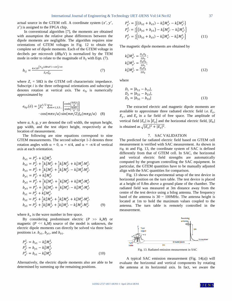
b. Location of Grounding
The location of the ground strap plays another important
factor to optimize the effectiveness of grounding. In this
particular case, the ground strap shall be placed near to all
interconnection points so that the electromagnetic noise from
the interconnection points will instantly be diverted to ground.
Fig. 7 shows placement of copper tape for location P1 and P2.
The corresponding result in Fig. 8 indicates further
improvement on the cleanliness of the noise floor while
placing copper tape at both locations P1 and P2.
Fig. 7. Placement of copper ground
Fig. 8. Ambient noise for different ground locations
4.2. Suppression with Ferromagnetic Material
The result indicates grounding effective to partially
remove the external electromagnetic leakage. Therefore,
ferrimagnetic material is employed to suppress the common-
mode current which unintentionally formed at outer layer of
the interconnection cables, with the assumption that common-
mode cable current is the basis for electromagnetic
interference (EMI) and ferrite provides an excellent solution to
suppress EMI [6].
Fig. 9 presents the new noise floor after reducing external
leakages using ferromagnetic material and bundling all the
cables with Ni/Cu woven.
100 200 300 400 500 600 700 800 900 100010
20
30
40
50
60
Frequency (MHz)
Am
plit
ude (
dB
uV
)
No ground wire
Single wire
Ribbon cable
Copper tape
100 200 300 400 500 600 700 800 900 100010
20
30
40
50
60
Frequency (MHz)
Am
plit
ude (
dB
uV
)
No ground
P1
P2
Both
100 200 300 400 500 600 700 800 900 100010
20
30
40
50
60
70
80
Frequency (MHz)
Am
plit
ud
e (
dB
uV
)
Without ferrite & Ni/Cu woven
With ferrite
With ferrite & Ni/Cu woven
Copper
tape
P1 P2

International Journal of Engineering & Technology IJET-IJENS Vol:14 No:02 36
143502-2727-IJET-IJENS © April 2014 IJENS I J E N S
Fig. 9. Radiated emission before and after wrapping cables with ferrite
sheet
4.3. Double Shielded Cables
The previous result still shows the existence of
electromagnetic leakage at about 900MHz even after efforts
had been taken to eliminate it with shielding, grounding and
suppression using ferrite. Since these peaks appear across
GSM mobile phone frequencies, it is suspected that these
peaks originate from nearby base station. The cable
connecting the GTEM cell to spectrum analyzer is able to pick
up GSM signal. The condition can be improved using double
shielded cable as shown in Fig. 10.
Fig. 10. Use double shielded cable for better performance
5. RADIATED FIELD MEASUREMENT
After obtaining a clean noise floor, the FPGA chip was
mounted on the manipulator as shown in Fig. 11. The device
is rotated at three orthogonal orientations for optimizing
emission measurement. As the radiation pattern of the FPGA
chip is unknown. At each orientation, the device is further
rotated across its vertical axis for 0, 45 and 315 degrees. The
voltage of the emission is measured at the GTEM cell port
using spectrum analyzer.
To operate the FPGA chip, a toggle flip-flop (TFF) logic
circuit pattern was created for the chip configuration. The
circuit will occupy 20% of total the FPGA chip space so that it
will generate sufficient energy for the emission measurement.
The TFF circuit has two I/O terminals where the input
terminal is exercised with an external sinusoidal clock signal.
The clock frequency is 100 MHz and the output signal of the
TFF pattern is 50 Mhz.
Fig. 11. Measurement setup in GTEM cell
Fig. 12 shows the measured radiated emission that
captured in x, y and z positions. It is observed that the
frequency spectrum comprises fundamental clock frequency
with integration fundamental and harmonics of the output
signal. The data can now be used for further applications
because the effects of unwanted ambient noise have been
eliminated using the techniques described earlier in this paper.
It is assumed that the measured voltages are contributed by the
FPGA chip.
(a)
(b)
(c)
Fig. 12. Emission of FPGA chip at three orthogonal orientations, (a) x
axis, (b) y axis, and (c) z axis
6. Equivalent Emission Model
As rotating the FPGA chip in the GTEM cell, the
electromagnetic field emitted from the FPGA chip will couple
to differential dipole components and the TEM mode e0y of the
GTEM cell resulting potential at the cell port. However, the
measured GTEM voltages only contain electrical information
relative to the FPGA chip emission in the GTEM cell. We also
have known that the voltage is actually related to the current
source, i.e., electric and magnetic dipole moments as given by
( )
( ) (6)
Assuming the FPGA chip as a general source model, the
dipole modeling process can be carried out to approximate far
field for correlation between GTEM cell and semi anechoic
chamber. In particular, the FPGA chip is represented as a set
of dipole which comprises three electric moments , ,
and three magnetic moments , , as to the
100 200 300 400 500 600 700 800 900 100010
20
30
40
50
60
Frequency (MHz)
Am
plit
ud
e (
dB
uV
)
Single shielded cable
Double shielded cable
100 200 300 400 500 600 700 800 900 100015
20
25
30
35
40
45
50
55
60
Frequency (MHz)
Am
plit
ude (
dB
uV
/m)
0 degree
45 degree
-45 degree
100 200 300 400 500 600 700 800 900 100010
20
30
40
50
60
70
Frequency (MHz)
Am
plit
ude (
dB
uV
/m)
0 degree
45 degree
-45 degree
100 200 300 400 500 600 700 800 900 100010
20
30
40
50
60
70
80
Frequency (MHz)
Am
plit
ude (
dB
uV
/m)
0 degree
45 degree
-45 degree
International Journal of Engineering & Technology IJET-IJENS Vol:14 No:02 37
143502-2727-IJET-IJENS © April 2014 IJENS I J E N S
actual source in the GTEM cell. A coordinate system ( , ,
) is assigned to the FPGA chip.
In conventional algorithm [7], the moments are obtained
with assumption the relative phase differences between the
dipole moments are negligible. The algorithm requires nine
orientations of GTEM voltages in Fig. 12 to obtain the
complete set of dipole moments. Each of the GTEM voltage in
decibels per microvolt (dB V) is normalized by the TEM
mode in order to relate to the magnitude of bij with Eqn. (7).
( ( ) )
(7)
where Zc = 50 is the GTEM cell characteristic impedance.
Subscript i is the three orthogonal orientations and subscript j
denotes rotation at vertical axis. The e0y is numerically
approximated by
( )
⁄ ∑ [ (
)
(
)]
( ) ( ) ( ) (8)
where a, h, g, y are denoted the cell width, the septum height,
gap width, and the test object height, respectively at the
location of measurement.
The following are nine equations correspond to nine
GTEM measurements. The second subscript 1-3 denotes three
rotation angles with = 0, = /4, and = -/4 of vertical
axis at each orientation.
(9)
where is the wave number in free space.
By considering predominant electric (P koM) or
magnetic (P << koM) source of the model is unknown, the
electric dipole moments can directly be solved via three basic
positions i.e. , , and .
(10)
Alternatively, the electric dipole moments also are able to be
determined by summing up the remaining positions.
( )
( )
( )
(11)
The magnetic dipole moments are obtained by
;
;
(12)
where
| |, | |, | | (13)
The extracted electric and magnetic dipole moments are
available to approximate three radiated electric field i.e. ,
, and in a far field of free space. The amplitude of
vertical field | | is | | and the horizontal electric field, | |
is obtained as √| | | |
.
7. SAC VALIDATION
The predicted far radiated electric field based on GTEM cell
measurement is verified with SAC measurement. As shown in
Fig. 11 and Fig. 13, the coordinate system of SAC is defined
differently from that of GTEM cell. In SAC, the horizontal
and vertical electric field strengths are automatically
computed by the program controlling the SAC equipment. In
particular, the GTEM quantities have to be manually adjusted
align with the SAC quantities for comparison.
Fig. 13 shows the experimental setup of the test device in
horizontal position on the turn table. The test device is placed
at a height of 0.8m above a ground plane of the chamber. The
radiated field was measured at 3m distance away from the
centre of the test device using a bilog antenna. The frequency
band of the antenna is 30 ~ 100MHz. The antenna height is
located at 1m to hold the maximum values coupled to the
antenna. The turn table is remotely controlled in the
measurement.
Fig. 13. Radiated emission measurement in SAC
A typical SAC emission measurement (Fig. 14(a)) will
evaluate the horizontal and vertical components by rotating
the antenna at its horizontal axis. In fact, we aware the

International Journal of Engineering & Technology IJET-IJENS Vol:14 No:02 38
143502-2727-IJET-IJENS © April 2014 IJENS I J E N S
horizontal component is contributed by two axis alignments
where the adjacent horizontal source is always neglected in
the typical measurement.
3m
Measuring antenna DUT
Y
X
Z
(a)
3m
Measuring antenna DUT
Y
X
Z
(b) Fig. 14. Changing antenna position to account neglected horizontal
component; (a) typical antenna setup, (b) additional antenna setup for
SAC measurement
To account the missing adjacent horizontal component, we
perform additional measurement by changing the antenna
position in 90 degree across its vertical axis. The horizontal
component is obtained as √| | | |
as shown in Fig.
14(b).
Fig. 15 presents the comparison between GTEM data and
SAC data. The noise floor between the two environments is
similar to achieve meaningful comparison. The electric field
peaks frequency in the spectrum is matching well. However, it
generally observed that the GTEM cell able to capture
stronger emission as the shorter distance between the test
device and the antenna. Therefore, further work will be carried
out to establish correct factor for improving the agreement of
the peak value.
(a)
(b)
Fig. 15. Estimated radiated emission from FPGA chip in GTEM cell as compared to SAC measurement; (a) horizontal electric field intensity and
(b) vertical electric field intensity
CONCLUSION
In this paper, we have presented techniques to eliminate
electromagnetic noise from interfering the radiated emission
due to ICs in a GTEM cell. A proper shielding the IC test
board using metallic cavity combined with the usage of
grounding near interconnection points using low impedance
ground strap and cable shielding using ferrimagnetic
successfully removed the unwanted noise in the emission
measurement. The approximate horizontal and vertical electric
field via dipole moment technique has shown optimistic
insight correlation between GTEM cell and SAC. This work
provides a preliminary input in an effort to perform IC
emission measurement inside a GTEM cell as opposed to
mounting it on the GTEM wall based on IEC 61967.
ACKNOWLEDGEMENT
The authors wish to thank Multimedia Development
Corporation (MDeC) for the financial support and Altera
Corporation (M) Sdn. Bhd. for providing FPGA test board for
the research. The support by UTHM Research, Innovation,
Commercialization and Consultancy Office (ORICC) is also
acknowledged in providing the permission and fee to publish
this paper.
REFERENCES [1]. Standard EMC 61967-2. Integrated Circuits -- Measurement of
Electromagnetic Emissions, 150kHz to 1GHz -- Part 2: Measurement
of Radiated Emissions - TEM Cell and Wideband TEM Cell Method.
Int. Electrotech. Commiss. (2005). [2]. B. Deutschmann, H.P., and G. Langer. Near field measurements to
predict the electromagnetic emission of integrated circuits. Proc. 5th
Int. Workshop Electromgan. Compat. Integr. Cuicuits (2005). [3]. Haixiao, W., D.G. Beetner, and R.E. DuBroff. Prediction of Radiated
Emissions Using Near-Field Measurements. IEEE Transactions on
Electromagnetic Compatibility, (2011). 53(4): p. 891-899.
[4]. F. T. Ulaby, E.M., U. Ravaioli. Fundamentals of Applied
Electromagnetics. 6th Edition: Pearson (2012). p.80-83
[5]. Paul, C.R., Introduction to Electromagnetic Compatibility. 2nd Edition (2006): John Wiley & Sons. p.718-721
[6]. Hubing, T.H. Bundled cable parameters and their impact on EMI
measurement repeatability. IEEE International Symposium on Electromagnetic Compatibility. (1990). p. 576-580
[7]. Wilson, P., On correlating TEM cell and OATS emission
measurements. IEEE Transactions on Electromagnetic Compatibility. (1995). 37(1): p. 1-16.
100 200 300 400 500 600 700 800 900 1000-10
0
10
20
30
40
50
60
70
80
Frequency (MHz)
Ra
dia
ted
Em
issio
n (
dB
uV
/m)
SAC
GTEM
100 200 300 400 500 600 700 800 900 1000-10
0
10
20
30
40
50
60
70
80
Frequency (MHz)
Ra
dia
ted
Em
issio
n (
dB
uV
/m)
SAC
GTEM