Embed Size (px)
Citation preview
1
Exploiting Dual-Gate Ambipolar CNFETs for ScalableMachine Learning Classification
Farid Kenarangi1, Xuan Hu2, Yihan Liu3, Jean Anne C. Incorvia3, Joseph S. Friedman2, and Inna Partin-Vaisband1
1University of Illinois at Chicago2University of Texas at Dallas3University of Texas at Austin
Abstract—Ambipolar carbon nanotube based field-effect tran-sistors (AP-CNFETs) exhibit unique electrical characteristics,such as tri-state operation and bi-directionality, enabling systemswith complex and reconfigurable computing. In this paper, AP-CNFETs are used to design a mixed-signal machine learn-ing (ML) classifier. The classifier is designed in SPICE withfeature size of 15 nm and operates at 250 MHz. The systemis demonstrated based on MNIST digit dataset, yielding 90%accuracy and no accuracy degradation as compared with theclassification of this dataset in Python. The system also exhibitslower power consumption and smaller physical size as comparedwith the state-of-the-art CMOS and memristor based mixed-signal classifiers.
Index Terms— Ambipolar carbon nanotube, mixed-signal,machine learning, logistic classifier, low area.
I. INTRODUCTION
POWER consumption and physical size of integrated circuits(ICs) is an increasing concern in many emerging ML
applications, such as, autonomous vehicles, security systems,and Internet of Things (IoT). Existing state-of-the-art archi-tectures for digital classification, are highly accurate and canprovide high throughput [1]. These classifiers, however, exhibithigh power consumption and occupy a relatively large areato accommodate complex ML models. Alternatively, mixed-signal classifiers have been demonstrated to exhibit orders ofmagnitude reduction in power and area as compared to digitalclassifiers with prediction accuracy approaching the accuracyof digital classifiers [2]–[9]. While significant advances havebeen made at the ML circuit and architecture levels (e.g.,in-SRAM processing [2], comparator based computing [3],and switched-capacitor neurons [4]), the lack of robust, ML-specific transistors is a primary concern in ML training andinference with all conventional CMOS technologies. To effi-ciently increase the density and power efficiency of modernML ICs while enabling complex computing, emerging tech-nologies should be considered.
While the non-volatility of memristors has proven quiteattractive for storing the weights required for feature-weightmultiplication [10]–[13], field-effect transistors provide severaladvantages over memristors for ML. First, transistors providea broader range of linear tuning of resistance, thereby bettermatching ML models. Second, transistors are not subject tothe deleterious aging that deteriorates memristor behaviorover time. Finally, the connectivity between feature-weight
Fig. 1. Forward-transfer characteristics (bottom gate voltage variesfrom -80 V to 80 V) evolution of a BP FET measured at Vsd =100 mVin logarithmic scale with increasing Cs2CO3 thickness from 0 to1.5 nm [14].
multiplication layers requires electrical signal gain, whichcannot be provided by memristors; transistors can be usedfor such interlayer connections, thereby enabling a monolithicintegrated circuit that can be fabricated efficiently. Of particu-lar interest for on-chip classification are ambipolar devices.Owing to unique electrical characteristics, as described inSection II, ambipolar devices are expected to provide efficienton-chip training and inference solutions and reduce design androuting complexity of ML circuits.
A carbon nanotube ambipolar device has been reportedas a potential candidate for controllable ambipolar devicesbecause of its satisfying carrier mobility and its symmetricand good subthreshold ambipolar electrical performance [15].Based on the dual-gate CNT device’s electrical performance,a library of static ambipolar CNT dual-gate devices basedon generalized NOR-NAND-AOI-OAI primitives, which ef-ficiently implements XOR-based functions, has been reported,indicating a performance improvement of ×7, a 57% reductionin power consumption, and a ×20 improvement in energy-delay product over the CMOS library [16].
Besides CNTs, some 2D semiconductors such as MoS2,WS2, WSe2 and black phosphorus (BP) are also reportedas ambipolar semiconductors at room temperature. Surfacetransfer doping and using different source and drain contact
arX
iv:1
912.
0406
8v1
[cs
.ET
] 9
Dec
201
9

2
metal are reported as two effective way to modulate itsambipolar characteristics to move the subthreshold curve’ssymmetric point to Vbottomgate = 0 and reduce the differencebetween the n-branch and p-branch saturation current. Fig.1 indicates that undoped multiplayer BP FETs’ saturationcurrent and mobility in the n-branch are much lower thanthat of the p-branch. However, Cs2CO3 layers deposited overBP serve as an efficient n-type surface dopant to improve theelectron transport in the BP devices, thereby inducing eithera more balanced ambipolar or even-transport-dominated FETbehavior [14]. Also, by using Ni as the source metal and Pdas the drain contact, the experimental transfer characteristicscurve of a multilayer WSe2 FET indicates this configurationallows for ambipolar characteristics with both the electron andhole conduction current levels being similar [17].
Existing results exploit the switching characteristics of theAP-CNFETs for enhancing digital circuits [16], [18]. In thiswork, we repurpose the AP-CNFET device for neuromorphiccomputing. Owing to the dual gate structure, AP-CNFETsignificantly increases the overall density of analog ML ICs,simplifies routing, and reduces power consumption. To the bestof the authors knowledge, the AP-CNFET based ML frame-work is the first to demonstrate a multiplication-accumulation(MAC) operation with single-device-single-wire configuration.Note that in CMOS classifiers at least two sensing lines arerequired to separately accumulate results of multiplicationwith positive and negative weights. Furthermore, additionalcircuitry is required to process the signals from the individualsensing lines into a final prediction. Alternatively, in memristorbased classifiers, a crossbar architecture is typically used witha single sensing line per class. With this configuration, onlypositive (or negative) feature weights are, however, utilized.Thus, additional non-linear thresholding circuits are requiredfor extracting the final decision.
The rest of the paper is organized as follows. The devicebackground and electrical characteristics of AP-CNFET deviceare presented in Section II. The proposed scheme for utilizingAP-CNFETs for on-chip classification is described in SectionIII. The classifier is evaluated based on classification ofcommonly used Modified National Institute of Standards andTechnology (MNIST) dataset, as explained in Section IV.Finally, the paper is concluded in Section V.
II. BACKGROUND
A. AP-CNFET Device
Depending on the gate voltage, an ambipolar device allowsboth electrons and holes to flow from source to drain becauseof its narrow Schottky barrier width, as small as a couple ofnanometers, between metal contacts and the channel [15]. Fig.2 shows the schematic of a top-bottom dual-gate ambipolardevice. In contrast to a normal single-gate-control transistor,the bottom gate plays an important role in determining thetype of majority carrier and on current. This dual-gate device’selectrical characteristic can be understood by the schematicband diagrams shown in Fig. 3. For a sufficiently negative(positive) bottom gate voltage, the Schottky barrier is thinnedenough to allow for holes (electrons) tunneling from the source
Fig. 2. Schematic of a top-bottom dual-gate ambipolar device.
Fig. 3. Schematic band diagrams of a dual-gate for bottom gatevoltage < 0 and > 0. The solid and dashed lines at the middleregion show how the top gate voltage switches the operating state byallowing or stopping the current flow [15].
contact into the channel to the drain. By tuning the top gatevoltage more positive (negative) to alter the barrier height forcarrier transport across the channel, the top gate can switchbetween the ON and OFF operating states.
B. Electrical Characteristics of the AP-CNFET
As compared with a conventional MOSFET, an AP-CNFETs exhibits two unique characteristics as explainedbelow.
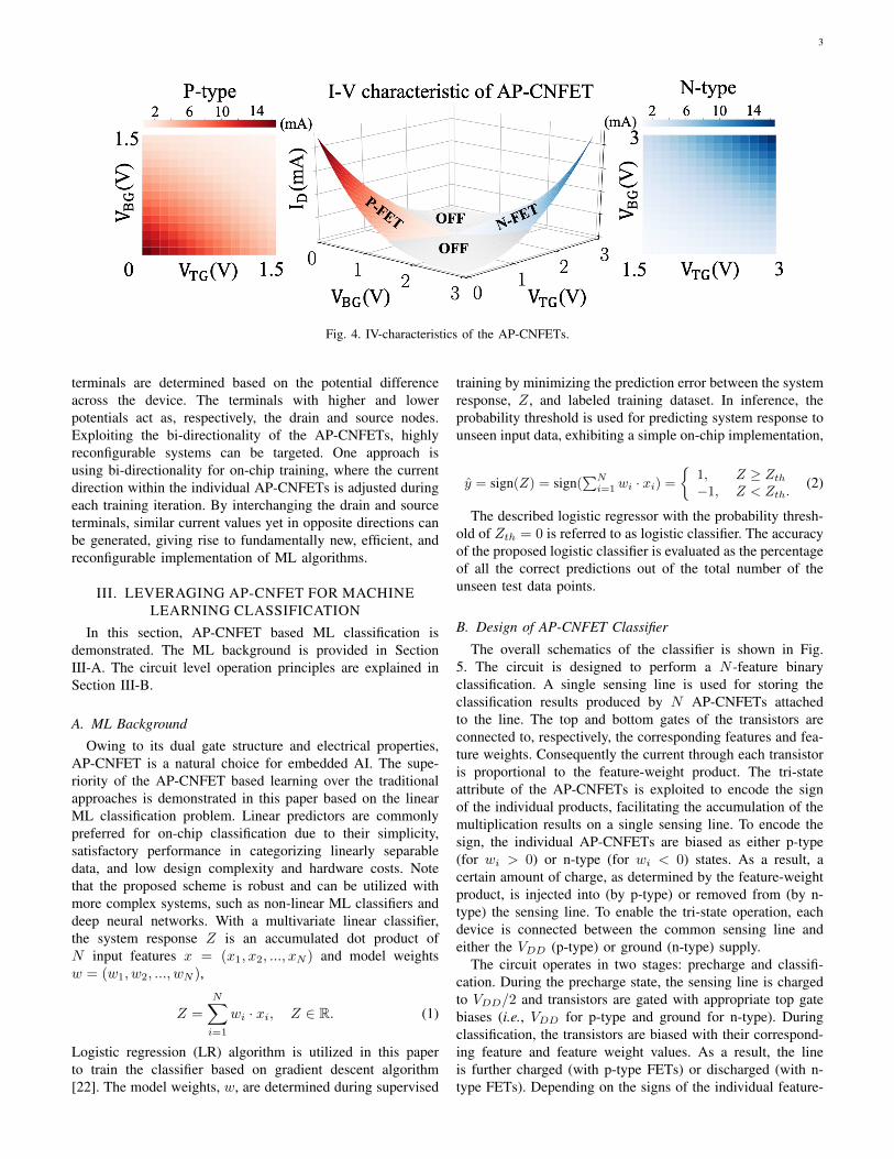
Tri-State Operation. Due to ambipolarity of an AP-CNFET, the majority carriers in the device can be eitherelectrons or holes, depending upon the gate biases. The samedevice can, therefore, operate as n-type (majority carriers areelectrons) or p-type (majority carriers are holes) FET. The I-Vcharacteristics (i.e., drain current ID versus top gate voltageVTG and bottom gate voltage VBG) of a single AP-CNFETare shown in Fig. 4, exhibiting p-type (red), n-type (blue),and OFF (gray) operational regions. In typical mixed-signalML classifiers, positive and negative classification decisionsare separately accumulated on the individual sensing lines [2],[5], [6], [19]. Thus, at least two wires are required for a singleMAC operation. Alternatively, with the proposed structure,the unique tri-state operation of AP-CNFETs is leveraged formerging the sensing lines, significantly reducing the routingcomplexity and area overhead, as described in Section III.
Bi-directionality. Another unique characteristic, is the bi-directionality of the device [20], [21]. The drain and source
3
Fig. 4. IV-characteristics of the AP-CNFETs.
terminals are determined based on the potential differenceacross the device. The terminals with higher and lowerpotentials act as, respectively, the drain and source nodes.Exploiting the bi-directionality of the AP-CNFETs, highlyreconfigurable systems can be targeted. One approach isusing bi-directionality for on-chip training, where the currentdirection within the individual AP-CNFETs is adjusted duringeach training iteration. By interchanging the drain and sourceterminals, similar current values yet in opposite directions canbe generated, giving rise to fundamentally new, efficient, andreconfigurable implementation of ML algorithms.
III. LEVERAGING AP-CNFET FOR MACHINELEARNING CLASSIFICATION
In this section, AP-CNFET based ML classification isdemonstrated. The ML background is provided in SectionIII-A. The circuit level operation principles are explained inSection III-B.
A. ML Background
Owing to its dual gate structure and electrical properties,AP-CNFET is a natural choice for embedded AI. The supe-riority of the AP-CNFET based learning over the traditionalapproaches is demonstrated in this paper based on the linearML classification problem. Linear predictors are commonlypreferred for on-chip classification due to their simplicity,satisfactory performance in categorizing linearly separabledata, and low design complexity and hardware costs. Notethat the proposed scheme is robust and can be utilized withmore complex systems, such as non-linear ML classifiers anddeep neural networks. With a multivariate linear classifier,the system response Z is an accumulated dot product ofN input features x = (x1, x2, ..., xN ) and model weightsw = (w1, w2, ..., wN ),
Z =
N∑i=1
wi · xi, Z ∈ R. (1)
Logistic regression (LR) algorithm is utilized in this paperto train the classifier based on gradient descent algorithm[22]. The model weights, w, are determined during supervised
training by minimizing the prediction error between the systemresponse, Z, and labeled training dataset. In inference, theprobability threshold is used for predicting system response tounseen input data, exhibiting a simple on-chip implementation,
y = sign(Z) = sign(∑N
i=1 wi · xi) =
{1, Z ≥ Zth
−1, Z < Zth.(2)
The described logistic regressor with the probability thresh-old of Zth = 0 is referred to as logistic classifier. The accuracyof the proposed logistic classifier is evaluated as the percentageof all the correct predictions out of the total number of theunseen test data points.
B. Design of AP-CNFET Classifier
The overall schematics of the classifier is shown in Fig.5. The circuit is designed to perform a N -feature binaryclassification. A single sensing line is used for storing theclassification results produced by N AP-CNFETs attachedto the line. The top and bottom gates of the transistors areconnected to, respectively, the corresponding features and fea-ture weights. Consequently the current through each transistoris proportional to the feature-weight product. The tri-stateattribute of the AP-CNFETs is exploited to encode the signof the individual products, facilitating the accumulation of themultiplication results on a single sensing line. To encode thesign, the individual AP-CNFETs are biased as either p-type(for wi > 0) or n-type (for wi < 0) states. As a result, acertain amount of charge, as determined by the feature-weightproduct, is injected into (by p-type) or removed from (by n-type) the sensing line. To enable the tri-state operation, eachdevice is connected between the common sensing line andeither the VDD (p-type) or ground (n-type) supply.
The circuit operates in two stages: precharge and classifi-cation. During the precharge state, the sensing line is chargedto VDD/2 and transistors are gated with appropriate top gatebiases (i.e., VDD for p-type and ground for n-type). Duringclassification, the transistors are biased with their correspond-ing feature and feature weight values. As a result, the lineis further charged (with p-type FETs) or discharged (with n-type FETs). Depending on the signs of the individual feature-

4
Fig. 5. The overall schematics of the proposed N -dimensional, binaryclassifier. The top and bottom gates of the AP-CNFETs are connectedto, respectively, the corresponding features, xi, and feature weights,wi. To encode the weight sign, the individual AP-CNFETs are biasedas either p-type (wi > 0) or n-type (wi < 0) states. The circuitoperates in two stages: precharge and classification (see the red VSW
waveform). During the precharge state, the sensing line is charged toVDD/2. The classification decision is made during the classificationphase based on the line voltage level as compared to VDD/2 (seethe blue Vsen waveform). The final decision between two classes ismade based on the output of the buffers chain (see the black Vvote
waveform).
weight products, the sensing line accumulates or dissipates acertain amount of charge, saturating at, respectively, higher(> VDD/2) or lower (< VDD/2) voltage Vsen. Consequently,the classification decision is determined as,
y =
{+1, Vsen > VDD/2−1, Vsen < VDD/2.
(3)
To extract the final decision, a non-inverting buffer isconnected to the sensing line, as shown in Fig. 5. ForVsen > VDD/2, the output of the sensing line is forced toVvote = VDD. The line is forced to Vvote = 0 for Vsen <VDD/2. Note that using a single sensing line eliminates aconventional classification stage where the voltage on thepositive and negative sensing lines is compared to determinethe final binary classification result. The proposed circuit
is also more resilient to process, voltage, and temperature(PVT) variations as compared with state-of-the-art mixed-signal classifiers, since it only uses inverters to extract thefinal decision. Alternatively, in state-of-the-art classifiers (e.g.,[2], [3]), comparators, are utilized to extract the final decision.The correct operation of such comparators highly relies onsymmetry of the circuit, exhibiting significant offset underPVT variations. To mitigate the sensitivity to PVT variations,additional compensating rows are utilized in the existing MLclassifiers. [2]. The small power consumption and area of theseML classifiers is, therefore, traded off for higher classificationaccuracy.
Linearity of the individual AP-CNFETS is critical forcorrect classification of the input features. Albeit the semi-linear dependence of output current on the gate biases acrossthe full voltage range of operation (see Fig. 4), AP-CNFETexhibits no degradation in classification accuracy as comparedto classification accuracy in Python, as presented in SectionIV. Alternatively, utilization of the wide bias region allowsfor quantization of features and feature weights with largerquantization step, increasing the resilience of the circuit toPVT variations. In this paper, five-bit resolution is consideredfor quantizing features and feature weights with a 40 mV stepsize. To quantize the features and feature weights, resistivevoltage dividers are used. While feature weight connectionsare set to fixed values, multiplexer (MUX) units are used toupdate the features within each classification period. Note thatto support reconfigurable feature weights, memory units (forstoring the weights) along with multiplexer units (for selectingthe desired weights) can be utilized. While power overhead isnegligible with this approach, the overall area is expected tobe increased by a factor of four.
IV. SYSTEM DEMONSTRATION AND RESULTS
The classifier is designed in SPICE and evaluated based on acommonly used MNIST dataset. The dataset and preprocessingsteps are described in Section IV-A. The overall system andSPICE simulation results are presented in Section. IV-B.
A. Dataset and Preprocessing Steps
MNIST is a large dataset of digit images commonly usedfor evaluating the effectiveness of ML ICs. MNIST containsimages of 70,000 handwritten digits, ranging between 0 and9. Each digit comprises 784 (28 × 28) image pixels. Thedefault training and test datasets comprise, respectively, 60,000and 10,000 digits. Out of the 60,000 training observations,45,000 and 15,000 are used for, respectively, the training andvalidation of the proposed system.
One versus one classification scheme [23], is used todiscriminate the 10-class MNIST dataset. A K-class, oneversus one classifier is designed with K(K − 1)/2 binaryclassifiers for pairwise discrimination of the digits. Eachbinary classifier votes for a single class and the class withhighest number of votes is selected as the final classificationdecision. Utilizing the full set of features (i.e., 784 features),accuracy of 94% can be achieved on MNIST test set with10(10 − 1)/2 = 45 binary logistic classifiers. Alternatively,

5
Fig. 6. An example of MNIST digit image. Out of the total 784features, 720 features are dumped during the downsampling stage.The selected 64 (8 × 8) features are shown by red squares.
Fig. 7. The selected number of features for each binary classifier (i.e.,i-j classifier).
a subset of the 784 features (i.e., 23 features on average)is used in this paper, trading off the performance (less than4.6% accuracy degradation) for power and area efficiency(×(784/23) = ×34 less transistors). The subset of featuresis selected in a two-step approach: downsampling and featureselection. First, the features are uniformly downsampled from28 × 28 pixels to 8 × 8 pixels, as shown in Fig. 6. Thedownsampling of features significantly reduces the requiredhardware resources (e.g., 12 times less transistors is required)in exchange for 2.8% accuracy degradation. A greedy featureselection algorithm, sequential backward selection (SBS) [24],is used to select those most informative features (out of theremaining 64 features) for each binary classifier. As a result,the 8 × 8 features are reduced on average to 23 featuresper digit. Note that the number of selected features variesamong the MNIST digits. For example, the digits 3 and 4tend to look much more alike than the digits 0 and 1. Thus,significantly more features is selected for the 3-vs-4 binaryclassifier (44 features) than for the 0-vs-1 binary classifier (6features). Comparing with other well-known feature selection
Fig. 8. A schematic diagram of the proposed AP-CNFET based 10-class classifier. An array of 64× 45 AP-CNFETs is used to performthe feature-weight products. The transistors biased in n-type and p-type regions are shown by, respectively, the blues and red circles.The transistors that have been removed as a result of SBS featurereduction are shown by white circles.
algorithms (e.g., Fisher information [25]), SBS is determinedto select the most informative features. Alternatively, SBS is aniterative greedy algorithm and is computationally expensive.For example, completing SBS on the original feature set of28× 28 pixels requires 306,936 training iterations and 72 day(as extrapolated on shorter runs) on Intel Core i7-7700 CPU.Alternatively, with downsampled feature space only 2,016training iterations which are completed within three hours onIntel Core i7-7700 CPU. The preferred set of features for eachbinary classifier is shown in Fig. 7, exhibiting an average of23 features per classifier.
B. System Demonstration and Simulation Results
The schematic representation of the overall system is shownin Fig. 8, comprising of AP-CNFET array to perform feature-weight products, voltage dividers to provide quantized featuresand feature weights, and buffers to extract the individual votesof each binary classifier. The proposed system comprises 45binary classifiers with a total of 1,021 AP-CNFETs utilized forthe feature-weight products (shown by red and blue circlesin Fig. 8). The product results are accumulated within the45 sensing lines (one for each binary classifier). The systemoccupies 3.8µm2 as estimated based on transistor count and

6
Fig. 9. Ten consecutive classifications of digits in MNIST dataset, as extracted based on SPICE simulations. For each classification, theheight of the bars corresponds to the number of votes collected to each class. Note that total number of votes is 45 and equals to the totalnumber of binary classifiers. Within a single classification period, the ith class, can get up to nine votes.
consumes 295 pJ energy per digit classification. Accuracy of90% is observed in SPICE on test set of 10,000 unseendigits, as compared with the theoretical classification accuracyof 90% obtained on the low resolution data set in Python.The confusion matrices obtained with Python and SPICEfor the 10,000-digit test set are shown in Fig. 10. Note thesimilarities of the decisions extracted by SPICE and Python.The classifier is designed to operate at 250 MHz, producing asingle digit classification per cycle. The extracted votes andresultant decisions are shown in Fig. 9 for ten consecutiveclassifications, as extracted from SPICE. Each binary classifiervotes for a single class. Thus, the total number of votesequals to the number of binary classifiers. Final decision ismade based on the class with highest number of votes withineach classification period, as shown in the Fig. 9. Note thesimilarity of the incorrectly classified images (‘4’ and ‘2’) tothe predicted labels (‘6’ and ‘8’, respectively).
Performance characteristics are listed in Table I for theproposed system along with the existing state-of-the-art con-ventional CMOS and emerging device memristor based clas-sifiers [3], [13]. For fair comparison, total current per de-cision (energy divided by supply voltage) and the systemarea normalized by squared form factor are also shown inTable I. The total current per decision with the proposedclassifier is approximately 5.4 times lower as compared withstate-of-the-art MOSFET approaches. Similarly, area savingsrange between ×15 and ×859 as compared to, respectively,MOSFET and memristor based classifiers, as shown in TableI. Alternatively, the proposed classifier exhibits only 2% loweraccuracy as compared with the artificial neural network (ANN)based classifiers in [13].
Fig. 10. Confusion matrices obtained by classifying MNIST in, (a)Python, and (b) SPICE.
V. CONCLUSIONS
Increasing the device density and power efficiency hasbecome challenging as the conventional CMOS scaling ap-proaches its physical limits. Alternatively, emerging devices,such as AP-CNFETs are inherently intelligent. The seamlessmapping of the AI logic primitives onto AP-CNFET increasesby orders of magnitude the embedded AI per transistor.
To the best of the authors knowledge, the proposed systemis the first to demonstrate ML classification with a singlesensing line. To evaluate the system, a multi-class logisticclassifier is designed in SPICE and demonstrated on MNISTdataset. The classifier uses 1,021 AP-CNFETs (×17 reductionin the transistor count as compared with state-of-the-art CMOSbased classifiers [2], [3]) and generates predictions at 250MHz. The system exhibits 295 pJ energy consumption andoccupies 3.8µm2 as estimated based on the transistor count inSPICE. With the proposed configuration, the reduced MNIST

7
TABLE I: System characteristics of the proposed and a state-of-the-art CMOS and memristor based ML classifier.
[13] [3] Current work
Device Memristor MOSFET AP-CNFET
Dataset MNIST MNIST MNIST
Technology 180 nm 130 nm 15 nm
Algorithm ANN Ada-boost LR
Accuracy 92% 90% 90%
Offset from the idealaccuracy -1% 0% 0%
Number of features 784 48 64
Supply voltage 1 V 1.2 V 3 V
Speed 3.33 KHz 1.3 MHz 250 MHz
Cos
ts
Energy 24µJ∗ 543 pJ 295 pJ∗∗
Total current per decision 24µA·sec 453 pA·sec 98 pA·sec
Area 8,364µm2 246,792µm2 3.8µm2∗∗
Normalized area 0.26µm2/nm2 14.6µm2/nm2 0.017µm2/nm2
∗ extrapolated based on the numbers reported in [13] for a network withfour input neurons and ten output neurons.∗∗ overhead reported for MAC array. Note that the overheads of the systemis dominated by MAC array.
dataset is classified with no reduction in the overall predictionaccuracy as compared with the theoretical Python results.
Theoretical bounds on classification accuracy are a strongfunction of the classification algorithm. In this paper, linearclassification is demonstrated as a proof of concept of AP-CNFET based AI. The theoretical accuracy with linear clas-sifiers is however limited to 94% using the default dataset ofall the 784 MNIST features [26]. Higher accuracy (> 98%)can be achieved with more complex algorithms, such asnon-linear support vector machines (SVM) and deep neuralnetworks (DNNs). Similar to linear classifiers, the operationof these complex network is dominated by feature-weightmultiplication and product accumulation. The proposed frame-work is expected to significantly increase the AI density,while reducing the power and area overheads in complex MLnetworks.
REFERENCES
[1] J. Lee et al., “Unpu: An energy-efficient deep neural network acceleratorwith fully variable weight bit precision,” IEEE J. Solid-State Circuits,vol. 54, no. 1, pp. 173–185, Oct 2018.
[2] J. Zhang, Z. Wang, and N. Verma, “In-memory computation of amachine-learning classifier in a standard 6T SRAM array,” IEEE J.Solid-State Circuits, vol. 52, no. 4, pp. 915–924, Apr 2017.
[3] Z. Wang and N. Verma, “A low-energy machine-learning classifier basedon clocked comparators for direct inference on analog sensors,” IEEETrans. Circuits Syst. I, Reg. Papers, vol. 64, no. 11, pp. 2954–2965, Jun2017.
[4] D. Bankman et al., “An always-on 3.8 µJ/86% CIFAR-10 mixed-signalbinary CNN processor with all memory on chip in 28nm CMOS,” inIEEE Int. Solid-State Circuits Conf. (ISSCC) Dig. Tech. Papers, Feb2018, pp. 222–224.
[5] F. Kenarangi and I. Partin-Vaisband, “A single-MOSFET MAC for con-fidence and resolution (CORE) driven machine learning classification,”arXiv preprint arXiv:1910.09597, Oct 2019.
[6] K. Kang and T. Shibata, “An on-chip-trainable gaussian-kernel analogsupport vector machine,” IEEE Trans. Circuits Syst. I, Reg. Papers,vol. 57, no. 7, pp. 1513–1524, Jul 2009.
[7] S. K. Gonugondla, M. Kang, and N. R. Shanbhag, “A variation-tolerantin-memory machine learning classifier via on-chip training,” IEEE J.Solid-State Circuits, vol. 53, no. 11, pp. 3163–3173, Sep 2018.
[8] M. Kang et al., “A multi-functional in-memory inference processorusing a standard 6T SRAM array,” IEEE J. Solid-State Circuits, vol. 53,no. 2, pp. 642–655, Jan 2018.
[9] A. Amaravati et al., “A 55-nm, 1.0–0.4 v, 1.25-pj/mac time-domainmixed-signal neuromorphic accelerator with stochastic synapses forreinforcement learning in autonomous mobile robots,” IEEE J. Solid-State Circuits, vol. 54, no. 1, pp. 75–87, Dec 2018.
[10] M. Hu et al., “Memristor-based analog computation and neural networkclassification with a dot product engine,” Advanced Materials, vol. 30,no. 9, p. 1705914, Jan 2018.
[11] S. Yu et al., “Scaling-up resistive synaptic arrays for neuro-inspiredarchitecture: challenges and prospect,” in Int. Electron Devices Meeting,Dec 2015, pp. 17–3.
[12] S. Agarwal et al., “Resistive memory device requirements for a neuralalgorithm accelerator,” in Int. Joint Conf. on Neural Networks, Jul 2016,pp. 929–938.
[13] O. Krestinskaya, K. N. Salama, and A. P. James, “Learning in memristiveneural network architectures using analog backpropagation circuits,”IEEE Trans. Circuits Syst. I, Reg. Papers, vol. 66, no. 2, pp. 719–732,Sep 2018.
[14] D. Xiang et al., “Surface transfer doping induced effective modulationon ambipolar characteristics of few-layer black phosphorus,” Naturecommunications, vol. 6, p. 6485, Mar 2015.
[15] Y.-M. Lin et al., “High-performance carbon nanotube field-effect tran-sistor with tunable polarities,” IEEE Trans. on Nanotech., vol. 4, no. 5,pp. 481–489, Sep 2005.
[16] M. H. Ben-Jamaa, K. Mohanram, and G. De Micheli, “An efficientgate library for ambipolar CNTFET logic,” IEEE Trans. Comput.-AidedDesign Integr. Circuits Syst., vol. 30, no. 2, pp. 242–255, Feb 2011.
[17] S. Das and J. Appenzeller, “WSe2 field effect transistors with enhancedambipolar characteristics,” Applied physics letters, vol. 103, no. 10, p.103501, Sep 2013.
[18] I. O’Connor et al., “CNTFET modeling and reconfigurable logic-circuitdesign,” IEEE Trans. Circuits Syst. I, Reg. Papers, vol. 54, no. 11, pp.2365–2379, Nov 2007.
[19] F. Kenarangi and I. Partin-Vaisband, “Leveraging independent double-gate FinFET devices for machine learning classification,” IEEE Trans.Circuits Syst. I, Reg. Papers, vol. PP, no. 99, pp. 1–12, Jul 2019.
[20] X. Hu and J. S. Friedman, “Transient model with interchangeability fordual-gate ambipolar CNTFET logic design,” in Int. Symp. on NanoscaleArch. (NANOARCH), Oct 2017, pp. 61–66.
[21] ——, “Closed-form model for dual-gate ambipolar CNTFET circuitdesign,” in Int. Symp. on Circuits and Syst. (ISCAS), Sep 2017, pp.1–4.
[22] J. A. Nelder and R. J. Baker, “Generalized linear models,” Encyclopediaof statistical sciences, vol. 4, Jul 2004.
[23] M. Aly, “Survey on multiclass classification methods,” Neural Netw,vol. 19, pp. 1–9, 2005.
[24] S. Raschka and V. Mirjalili, Python Machine Learning. Birmingham,U.K.: Packt, 2017.
[25] I. Guyon and A. Elisseeff, “An introduction to variable and featureselection,” J. Mach. Learn. Res., vol. 3, pp. 1157–1182, Jan 2003.
[26] kaggle Inc. (2018) Public Leaderboard: MNIST. [Online]. Available:https://www.kaggle.com/numbersareuseful/public-leaderboard-mnist