Embed Size (px)
Citation preview

Experimental realization of an O-band compact polarization splitter and rotator
KANG TAN,1,2,* YING HUANG,2 GUO-QIANG LO,2 CHANGYUAN YU,1,3 AND
CHENGKUO LEE1
1Department of Electrical & Computer Engineering, National University of Singapore, Singapore 117583, Singapore 2Institute of Microelectronics, A*STAR (Agency for Science, Technology and Research), 2 Fusionopolis Way, #08-02 Innovis Tower, Singapore 138634, Singapore 3Department of Electronic and Information Engineering, The Hong Kong Polytechnic University, Hung Hom, Hong Kong *[email protected]
Abstract: We experimentally realize a compact wideband polarization splitter and rotator (PSR) with CMOS compatibility. The fabricated PSR is then tested by utilizing a fabrication-tolerant TE-pass on-chip polarizer we propose to practically solve the issue of accurately aligning the polarizations in fiber and modes on chip. Both of these polarization handling devices take the advantage of bend structure that confines TE mode better than TM mode. The fabricated PSR has a high TM-TE and TE-TE mode conversion efficiency of −0.4 dB and −0.2 dB at 1310 nm, while the extinction ratio is better than 18 dB and the broad bandwidth exceeds 100 nm. © 2017 Optical Society of America
OCIS codes: (130.0130) Integrated optics; (130.3120) Integrated optics devices; (230.5440) Polarization-selective devices.
References and links
1. A. Rickman, “The commercialization of silicon photonics,” Nat. Photonics 8(8), 579–582 (2014). 2. T. Baehr-Jones, T. Pinguet, P. Lo Guo-Qiang, S. Danziger, D. Prather, and M. Hochberg, “Myths and rumours of
silicon photonics,” Nat. Photonics 6(4), 206–208 (2012).3. T. Barwicz, M. R. Watts, M. A. Popović, P. T. Rakich, L. Socci, F. X. Kärtner, E. P. Ippen, and H. I. Smith,
“Polarization-transparent microphotonic devices in the strong confinement limit,” Nat. Photonics 1(1), 57–60(2007).
4. J. Wang, D. Bonneau, M. Villa, J. W. Silverstone, R. Santagati, S. Miki, T. Yamashita, M. Fujiwara, M. Sasaki,H. Terai, M. G. Tanner, C. M. Natarajan, R. H. Hadfield, J. L. O’Brien, and M. G. Thompson, “Chip-to-chipquantum photonic interconnect by path-polarization interconversion,” Optica 3(4), 407–413 (2016).
5. W. D. Sacher, T. Barwicz, B. J. F. Taylor, and J. K. S. Poon, “Polarization rotator-splitters in standard active silicon photonics platforms,” Opt. Express 22(4), 3777–3786 (2014).
6. Z. Su, E. Timurdogan, E. S. Hosseini, J. Sun, G. Leake, D. D. Coolbaugh, and M. R. Watts, “Four-portintegrated polarizing beam splitter,” Opt. Lett. 39(4), 965–968 (2014).
7. J. Wang, B. Niu, Z. Sheng, A. Wu, X. Wang, S. Zou, M. Qi, and F. Gan, “Design of a SiO2 top-cladding and compact polarization splitter-rotator based on a rib directional coupler,” Opt. Express 22(4), 4137–4143 (2014).
8. H. Guan, A. Novack, M. Streshinsky, R. Shi, Y. Liu, Q. Fang, A. E. Lim, G. Lo, T. Baehr-Jones, and M. Hochberg, “High-Efficiency Low-Crosstalk 1310-nm Polarization Splitter and Rotator,” IEEE Photonics Technol. Lett. 26(9), 925–928 (2014).
9. J. Wang, M. Qi, Y. Xuan, H. Huang, Y. Li, M. Li, X. Chen, Q. Jia, Z. Sheng, A. Wu, W. Li, X. Wang, S. Zou, and F. Gan, “Proposal for fabrication-tolerant SOI polarization splitter-rotator based on cascaded MMI couplers and an assisted bi-level taper,” Opt. Express 22(23), 27869–27879 (2014).
10. J. Wang, B. Niu, Z. Sheng, A. Wu, W. Li, X. Wang, S. Zou, M. Qi, and F. Gan, “Novel ultra-broadband polarization splitter-rotator based on mode-evolution tapers and a mode-sorting asymmetric Y-junction,” Opt. Express 22(11), 13565–13571 (2014).
11. G. Chen, L. Chen, W. Ding, F. Sun, and R. Feng, “Ultrashort slot polarization rotator with double paralleled nonlinear geometry slot crossings,” Opt. Lett. 38(11), 1984–1986 (2013).
12. D. Dai and H. Wu, “Realization of a compact polarization splitter-rotator on silicon,” Opt. Lett. 41(10), 2346–2349 (2016).
13. Y. Huang, J. Song, X. Luo, T.-Y. Liow, and G.-Q. Lo, “CMOS compatible monolithic multi-layer Si3N4− on-SOI platform for low-loss high performance silicon photonics dense integration,” Opt. Express 22(18), 21859–21865(2014).
Vol. 25, No. 4 | 20 Feb 2017 | OPTICS EXPRESS 3234
#280824 https://doi.org/10.1364/OE.25.003234 Journal © 2017 Received 22 Nov 2016; revised 7 Jan 2017; accepted 10 Jan 2017; published 7 Feb 2017

14. K. Tan, Y. Huang, G.-Q. Lo, C. Lee, and C. Yu, “Compact highly-efficient polarization splitter and rotator based on 90° bends,” Opt. Express 24(13), 14506–14512 (2016).
15. L. H. Gabrielli, D. Liu, S. G. Johnson, and M. Lipson, “On-chip transformation optics for multimode waveguide bends,” Nat. Commun. 3, 1217 (2012).
16. Y. Ding, L. Liu, C. Peucheret, and H. Ou, “Fabrication tolerant polarization splitter and rotator based on a tapered directional coupler,” Opt. Express 20(18), 20021–20027 (2012).
17. Y. Huang, S. Zhu, H. Zhang, T.-Y. Liow, and G.-Q. Lo, “CMOS compatible horizontal nanoplasmonic slot waveguides TE-pass polarizer on silicon-on-insulator platform,” Opt. Express 21(10), 12790–12796 (2013).
18. W. D. Sacher, Y. Huang, L. Ding, T. Barwicz, J. C. Mikkelsen, B. J. F. Taylor, G.-Q. Lo, and J. K. S. Poon, “Polarization rotator-splitters and controllers in a Si3N4-on-SOI integrated photonics platform,” Opt. Express22(9), 11167–11174 (2014).
19. Y. Sun, Y. Xiong, and W. N. Ye, “Experimental demonstration of a two-mode (de)multiplexer based on a taper-etched directional coupler,” Opt. Lett. 41(16), 3743–3746 (2016).
1. Introduction
Silicon photonics provide the possibility of designing and fabricating ultra-compact and CMOS-compatible photonic building blocks with low manufacturing cost, which thus creates an expanding market, especially for current data center applications [1,2]. Among these building blocks, polarization splitter and rotator (PSR) is one of the key components for many polarization diversity photonic circuits including optical transceivers, as it essentially solves the problems of the high birefringence brought by silicon nanowire [3]. CMOS-compatible and compact PSR is highly desired for optical coherent transceivers in data center application as well as generation of polarization-entangled photons [4]. Till now, different design for PSRs have been proposed, including directional coupler (DC) [5–7], adiabatic tapers followed by Mach-Zehnder interferometer [8, 9], mode-evolution tapers followed by asymmetric Y-junction [10], slot waveguide [11], etc.
Commonly straight waveguides are exploited in these structures due to its relatively easy design rules [7, 12]. Recently Daoxin Dai and Hao Wu have realized a compact PSR by combining an adiabatic taper, an asymmetric DC, and a multimode interference mode filter, of which the length is ~70 µm and the loss of TM-TE conversion is 1.5 dB [12]. This PSR utilizes the air as upper cladding, which breaks the vertical symmetry and thus makes polarization rotation realized more easily. However, this does not match the most metal back-end-of-line (BEOL) processes, making it incompatible with other building blocks [13]. PSRs exploiting SiO2 as upper cladding have also been proposed recently for BEOL comparability, normally with a length of several tens or hundreds of micros [5]. Recently we have theoretically proposed a potential design of highly-efficient PSR utilizing the advantage of bend structure [14].
In this paper, we experimentally realize an O-band CMOS-compatible PSR utilizing ultra-compact double bends with a radius of 10 µm, which is then measured with the assistance of a fabrication-tolerant TE-pass on-chip polarizer we propose for accurately aligning the polarization in fiber and modes on chip. Instead of using special methods to avoid the different influences of bend structure on different modes [15], here we take the advantage of bends that confine fundamental TE mode better than fundamental TM mode to design ultra-compact PSR under the fabrication constraint brought by ultraviolet (UV) lithography. We fabricated this device in our institute by using CMOS-compatible fabrication process, and then measured it by exploiting edge coupling and aligning system [13]. Moreover, we further explore the advantage brought by bend and design a multi-bend structure naturally functioned as an on-chip fabrication-tolerant TE-pass polarizer, which provides a practical solution for accurately aligning the polarizations in fiber and modes on chip. By using the special designed TE-pass on-chip polarizer, we propose a procedure for accurate polarization alignment, which makes the good matching of experimental and simulation data [14] possible. The experimental results show that this ultra-compact PSR has a high TE-TE and TM-TE mode conversion efficiency of −0.2 dB and −0.4 dB at 1310 nm, while extinction
Vol. 25, No. 4 | 20 Feb 2017 | OPTICS EXPRESS 3235

ratio is better than 18 dB. Additionally, the 3-dB bandwidth of fabricated PSR covers all the O-band range.
2. Design and fabrication
We conduct the fabrication in IME of A*STAR. The fabrication starts with an 8-inch SOI wafer, which has 220-nm-thick single crystal silicon layer and 3-µm bottom oxide. We then use two steps of deep ultraviolet photolithography followed by reactive ion etching to fabricate the double bend structure. The inversed tapers are applied for the edge coupling between chip and lensed fibers, as inversed tapers provide broad bandwidth and low coupling loss.
Fig. 1. (a) SEM image of the whole PSR. (b) SEM photo of the bend structure.
Figure 1 shows the scanning electron microscope (SEM) image of the fabricated PSR based on double bends. The related parameters are listed as follows: the width of inner bend W1 = 400 nm, the bending radii R1 = 10 µm and R2 = 10.74 µm, the slab height H2 = 110 nm, the slab width of outer bend W3 = 285 nm, and rib width of outer bend W2 = 210 nm. The corresponding gap between the two bends has a width of Wg = 200 nm, due to the constrain of UV lithography [13]. Based on the theory described in [14], these parameters are designed and optimized in order to take the advantage of bend structure that confines fundamental TE mode better than TM mode, i.e. TE mode is well confined in the inner bend while TM mode is efficiently coupled and rotated to TE mode in the outer bend. The nanotaper is exploited for edge coupling, which has a length of 60 μm and a tip width of 200 nm. The polarization dependent coupling loss for TE mode and TM mode are measured to be 2.7 dB and 3 dB, respectively.
The polarization alignment in the testing is a tough issue as slight misalignment between polarizations in lensed fiber and modes on chip creates large difference in the measurement of the crosstalk and extinction ratio (ER) in PSR. Most previous experimental demonstrations of PSR exploit grating couplers for fiber-to-chip coupling because grating couplers can act as an on-chip polarizer so that only TE or TM mode can have a high coupling efficiency [8, 12, 16]. However, grating couplers normally have a narrow bandwidth and relatively large coupling loss, which makes it hard to be used for testing broad band devices.
Fig. 2. Schematic structure of proposed on-chip TE-pass polarizer, which comprises of 364 90° bends cascaded in series. Only the starting part is shown.
Vol. 25, No. 4 | 20 Feb 2017 | OPTICS EXPRESS 3236

Here we cmode better tpolarizer tolealignment comconfinement dTM mode expTE-pass polarfoundry servias a practical
3. Experime
In order to chFig. 3. Ampamplifier (PDsource. A freeonly one lineaconnected to emitted from connecting toTE mode porpower meter power and ou
Fig. 3
Fig. 4bend r
Figure 4 dTE and TM structures. Whrespectively f−2.9 dB when
continue to takthan TM modeerant to fabricamprises of 364difference betwperiences a higrizer almost imces. This tolerareference pola
ental setup a
haracterize the plified spontanDFA) with an ae space linear ar polarization guide the lineathe chip is th
o an in-line fibrtion and TM (OPM) and o
utput optical tra
3. Experimental se
4. The transmissionradius.
demonstrates thmode propag
hen TE mode for bend radiusn the bend radi
ke the advantae for building ation variation4 90° bends cween the fund
gher loss than fmmune to fabrance to fabrica
arizer to align th
nd testing re
fabricated PSneous emissioamplified wavepolarizer 1 wifrom the ASE
ar polarized lighen collected ber-based polarmode portion ptical spectrum
ansmission spe
etup for accurate po
n efficiency of pro
he experimentagating in the is injected, the of 7 µm and 5ius is 3 µm. As
age of bend stra simple but
ns. The on-chicascaded in seramental TE an
fundamental TEication variatio
ation conditionhe polarization
esults
R, we set up oon (ASE) noiselength range oith fiber conne
E source. Polaright to chip withby using the s
rization beam safter careful
m analyzer (Octrum.
olarization alignm
oposed on-chip TE
al results of traon-chip TE-p
e transmission 5 µm. Howevers shown by the
ructure that coeffective desi
ip TE-pass pories, as shownnd TM modes,E mode, whichon brought by
n in principle mns in fiber and
our measuremese from praseof O-band is uectors is then aization-maintaih lensed fiber tsame lensed fsplitter (PBS). polarization a
OSA) are used
ment and on-chip P
E-pass polarizer as
ansmission effipass polarizer
efficiency is −r, the transmis
e green line in
onfines fundamign of on-chipolarizer for pon in Fig. 2. D, naturally funh helps build any current state-makes it able to
modes on chip
ent system as eodymium-dopused as broadbapplied for filtining (PM) fibtip at the end.
fiber tip with This PBS can
alignment. Theto measure th
PSR measurement.
s a function of the
iciency for funexploiting m
−0.18 dB and −sion efficiencyFig. 4, the tran
mental TE p TE-pass larization ue to the
ndamental n on-chip of-the-art
o function p.
shown in ped fiber band light tering out
ber is then The light PM fiber
n split the en optical he output
e
ndamental multi-bend
−0.53 dB y drops to nsmission
Vol. 25, No. 4 | 20 Feb 2017 | OPTICS EXPRESS 3237
efficiency of TM mode is generally much smaller than that of TE mode. The polarization extinction ratio (PER) of the TE-pass polarizer can be defined by [17]
10( ) 10 log .TE
TM
TPER dB
T
= ×
(1)
where TET and TMT are the transmission efficiency for fundamental TE and TM modes,
respectively. Hence the PERs for fabricated on-chip TE-pass polarizer are 19.56 dB, 11.27 dB, and 7.87 dB for multi-bend structure with bend radius of 3 µm, 5 µm, and 7 µm, respectively. Considering that the auto-alignment system needs enough power to make the edge alignment accurate, we choose the multi-bend structure with a bend radius of 5 µm for aligning the polarizations in fiber and modes on chip.
Based on the specially designed multi-bend structure functioning as on-chip TE-pass polarizer, we propose a procedure to preciously align the polarizations in fiber and modes on chip, as polarization alignment is essentially the key part to determine how accurate the measurement would be.
As shown in Fig. 3, we firstly put free-space polarizer 2 in front of the input lensed fiber, while a near infrared (NIR) camera is exploited to collect the power of light passing through the free-space polarizer 2. After setting the free space polarizer 2 to allow TE mode to pass through, we roughly rotate the input lensed fiber to minimize the output power collected by NIR camera, which means the injected light is roughly aligned to TM mode for silicon chip. Then we put the silicon photonic chip on the testing stage, and connect the output lensed fiber directly to the OPM. We choose the waveguide with multi-bend structure for more accurate polarization alignment. The auto-aligning system is then started to automatically align the two lensed fibers with the waveguide on chip. The input lensed fiber is carefully rotated to find the minimum value of output power, which gives the maximum excitation of fundamental TM mode on chip. Furthermore, we need to align the output lensed fiber as well. After aligning the two lensed fibers to a strip reference waveguide, we tune the input polarization to stimulate fundamental TE mode on chip by rotating the free space polarizer 1 with 90° degrees. Then the in-line fiber-based PBS is inserted between the output lensed fiber and OPM. We choose one output port of PBS and connect it to the OPM. Then the output lensed fiber is carefully rotated for minimizing the output power exiting the selected output port of PBS. This output port of PBS connected to OPM collects the power of TM mode from the chip, and thus the other output port of PBS gives the power of TE mode from the chip.
After this careful polarization alignment, the optical transmission spectrum for different mode conversion can be measured by using OSA. The experimental results together with simulation data are shown in Fig. 5. The fabricated PSR is characterized by conversion efficiency (CE) and ER [5, 8, 18]. The CEs for the stimulated TM and TE mode are defined as
( )( )
10
10
( ) 10 log /.
( ) 10 log /
Cross Cross InputTM TE TM TE TM
Through Through InputTE TE TE TE TE
CE dB P P
CE dB P P
− −
− −
= ×
= × (2)
The ERs for the injected TM and TE mode are defined as
( )( )
10
10
( ) 10 log /.
( ) 10 log /
Cross Cross ThroughTM TE TM TE TM TE
Through Through CrossTE TE TE TE TE TE
ER dB P P
ER dB P P
− − −
− − −
= ×
= × (3)
1 2Port
Mode ModeP − is defined as the detected power of the mode 2 in the port when mode 1 is the
input.
Vol. 25, No. 4 | 20 Feb 2017 | OPTICS EXPRESS 3238
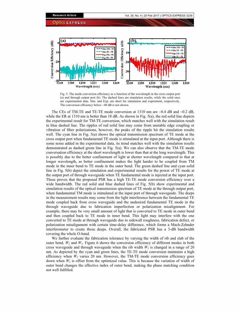
Fig. 5. The mode conversion efficiency as a function of the wavelength in the cross output port (a) and through output port (b). The dashed lines are simulation results, while the solid ones are experimental data. Sim. and Exp. are short for simulation and experiment, respectively. The conversion efficiency below −40 dB is not shown.
The CEs of TM-TE and TE-TE mode conversion at 1310 nm are −0.4 dB and −0.2 dB, while the ER at 1310 nm is better than 18 dB. As shown in Fig. 5(a), the red solid line depicts the experimental result for TM-TE conversion, which matches well with the simulation result in blue dashed line. The ripples of red solid line may come from unstable edge coupling or vibration of fiber polarizations, however, the peaks of the ripple hit the simulation results well. The cyan line in Fig. 5(a) shows the optical transmission spectrum of TE mode at the cross output port when fundamental TE mode is stimulated at the input port. Although there is some noise added in the experimental data, its trend matches well with the simulation results demonstrated as dashed green line in Fig. 5(a). We can also observe that the TM-TE mode conversation efficiency at the short wavelength is lower than that at the long wavelength. This is possibly due to the better confinement of light at shorter wavelength compared to that at longer wavelength, as better confinement makes the light harder to be coupled from TM mode in the inner bend to TE mode in the outer bend. The green dashed line and cyan solid line in Fig. 5(b) depict the simulation and experimental results for the power of TE mode at the output port of through waveguide when TE fundamental mode is injected at the input port. These proves that the proposed PSR has a high TE-TE mode conversion efficiency over a wide bandwidth. The red solid and blue dashed lines of Fig. 5(b) show experimental and simulation results of the optical transmission spectrum of TE mode at the through output port, when fundamental TM mode is stimulated at the input port of through waveguide. The deeps in the measurement results may come from the light interference between the fundamental TE mode coupled back from cross waveguide and the undesired fundamental TE mode in the through waveguide due to fabrication imperfection or polarization misalignment. For example, there may be very small amount of light that is converted to TE mode in outer bend and then coupled back to TE mode in inner bend. This light may interfere with the one converted to TE mode at through waveguide due to sidewall roughness, fabrication defect, or polarization misalignment with certain time-delay difference, which forms a Mach-Zehnder interferometer to create those deeps. Overall, the fabricated PSR has a 3-dB bandwidth covering the whole O-band.
We further evaluate the fabrication tolerance by varying the width of rib and slab of the outer bend, W2 and W3. Figure 6 shows the conversion efficiency of different modes in both cross waveguide and through waveguide when the rib width W2 is changed in a range of 20 nm. As depicted by the cyan and green lines, the TE-TE mode conversion maintains a high efficiency when W2 varies 20 nm. However, the TM-TE mode conversion efficiency goes down when W2 is offset from the optimized value. This is because the variation of width of outer bend changes the effective index of outer bend, making the phase matching condition not well fulfilled.
Vol. 25, No. 4 | 20 Feb 2017 | OPTICS EXPRESS 3239

Fig. 6. The CE as a function of rib width W2 at cross output port (a) and through output port (b). Sim. and Exp. are short for simulation and experiment, respectively. The wavelength is set to be 1310 nm.
The slab width is also varied to investigate its fabrication tolerance, as depicted in Fig. 7. The cyan and green lines in Fig. 7(b) demonstrate that both the experimental and simulation results of TE-TE mode conversion efficiency at 1310 nm almost remain the same when the slab width changes in a range of 20 nm, indicating the TE-TE mode conversion has a large tolerance towards the slab width. As shown by the blue and red line in Fig. 7(a), the TM-TE mode conversion efficiency drops when slab width varies 10 nm away from the optimized value. Therefore, the control of fabrication dimensions is needed in order to achieve a low loss below 0.5 dB. However, we can also modify the structure for improving the fabrication tolerance, such as applying the tapered structures [16, 19].
Fig. 7. The CE as a function of slab width W3 at cross output port (a) and through output port (b). Sim. and Exp. are short for simulation and experiment, respectively. The wavelength is set to be 1310 nm.
The good matching of the testing and simulation data further proves the effectiveness of proposed procedure for accurate alignment based on the specially designed multi-bend structure functioning as on-chip TE-pass polarizer.
4. Conclusion
In conclusion, we have experimentally realized a compact broadband PSR with CMOS compatibility. Instead of avoiding the influence brought by bend, we benefit from it for shortening the PSR and designing a multi-bend structure naturally functioning as an on-chip TE-pass polarizer. Based on this specially designed on-chip TE-pass polarizer, we have proposed a procedure to accurately align the polarizations in fiber and modes on chip, with which we have got the experimental results well matching the simulation data. The fabricated PSR has a high TM-TE and TE-TE mode conversion efficiency of −0.4 dB and −0.2 dB at 1310 nm, while the extinction ratio is better than 18 dB. Moreover, the fabricated PSR has a large 3-dB bandwidth covering the whole O-band range. Using different geometry parameters optimized by same design principles can build PSR with more compact structure as well as
Vol. 25, No. 4 | 20 Feb 2017 | OPTICS EXPRESS 3240

operating in other wavelength ranges, such as C-band, L-band, and mid-IR. These designs provide potential solutions for polarization handing in future large-scale high-density photonic integrated chips.
Funding
The authors acknowledge the financial support from the research grant of NRF-CRP15-2015-02 “Piezoelectric Photonics Using CMOS Compatible AlN Technology for Enabling The Next Generation Photonics ICs and Nanosensors” (WBS: R-263000C24281) at the National University of Singapore.
Vol. 25, No. 4 | 20 Feb 2017 | OPTICS EXPRESS 3241